JP5370214B2 - Video processing circuit, video processing method, liquid crystal display device, and electronic apparatus - Google Patents
Video processing circuit, video processing method, liquid crystal display device, and electronic apparatus Download PDFInfo
- Publication number
- JP5370214B2 JP5370214B2 JP2010039794A JP2010039794A JP5370214B2 JP 5370214 B2 JP5370214 B2 JP 5370214B2 JP 2010039794 A JP2010039794 A JP 2010039794A JP 2010039794 A JP2010039794 A JP 2010039794A JP 5370214 B2 JP5370214 B2 JP 5370214B2
- Authority
- JP
- Japan
- Prior art keywords
- pixel
- liquid crystal
- boundary
- video signal
- voltage
- Prior art date
- Legal status (The legal status is an assumption and is not a legal conclusion. Google has not performed a legal analysis and makes no representation as to the accuracy of the status listed.)
- Active
Links
Images


Classifications
-
- G—PHYSICS
- G09—EDUCATION; CRYPTOGRAPHY; DISPLAY; ADVERTISING; SEALS
- G09G—ARRANGEMENTS OR CIRCUITS FOR CONTROL OF INDICATING DEVICES USING STATIC MEANS TO PRESENT VARIABLE INFORMATION
- G09G3/00—Control arrangements or circuits, of interest only in connection with visual indicators other than cathode-ray tubes
- G09G3/20—Control arrangements or circuits, of interest only in connection with visual indicators other than cathode-ray tubes for presentation of an assembly of a number of characters, e.g. a page, by composing the assembly by combination of individual elements arranged in a matrix no fixed position being assigned to or needed to be assigned to the individual characters or partial characters
- G09G3/34—Control arrangements or circuits, of interest only in connection with visual indicators other than cathode-ray tubes for presentation of an assembly of a number of characters, e.g. a page, by composing the assembly by combination of individual elements arranged in a matrix no fixed position being assigned to or needed to be assigned to the individual characters or partial characters by control of light from an independent source
- G09G3/36—Control arrangements or circuits, of interest only in connection with visual indicators other than cathode-ray tubes for presentation of an assembly of a number of characters, e.g. a page, by composing the assembly by combination of individual elements arranged in a matrix no fixed position being assigned to or needed to be assigned to the individual characters or partial characters by control of light from an independent source using liquid crystals
- G09G3/3611—Control of matrices with row and column drivers
-
- G—PHYSICS
- G09—EDUCATION; CRYPTOGRAPHY; DISPLAY; ADVERTISING; SEALS
- G09G—ARRANGEMENTS OR CIRCUITS FOR CONTROL OF INDICATING DEVICES USING STATIC MEANS TO PRESENT VARIABLE INFORMATION
- G09G2310/00—Command of the display device
- G09G2310/02—Addressing, scanning or driving the display screen or processing steps related thereto
- G09G2310/0235—Field-sequential colour display
-
- G—PHYSICS
- G09—EDUCATION; CRYPTOGRAPHY; DISPLAY; ADVERTISING; SEALS
- G09G—ARRANGEMENTS OR CIRCUITS FOR CONTROL OF INDICATING DEVICES USING STATIC MEANS TO PRESENT VARIABLE INFORMATION
- G09G2320/00—Control of display operating conditions
- G09G2320/02—Improving the quality of display appearance
- G09G2320/0209—Crosstalk reduction, i.e. to reduce direct or indirect influences of signals directed to a certain pixel of the displayed image on other pixels of said image, inclusive of influences affecting pixels in different frames or fields or sub-images which constitute a same image, e.g. left and right images of a stereoscopic display
-
- G—PHYSICS
- G09—EDUCATION; CRYPTOGRAPHY; DISPLAY; ADVERTISING; SEALS
- G09G—ARRANGEMENTS OR CIRCUITS FOR CONTROL OF INDICATING DEVICES USING STATIC MEANS TO PRESENT VARIABLE INFORMATION
- G09G2320/00—Control of display operating conditions
- G09G2320/02—Improving the quality of display appearance
- G09G2320/0271—Adjustment of the gradation levels within the range of the gradation scale, e.g. by redistribution or clipping
-
- G—PHYSICS
- G09—EDUCATION; CRYPTOGRAPHY; DISPLAY; ADVERTISING; SEALS
- G09G—ARRANGEMENTS OR CIRCUITS FOR CONTROL OF INDICATING DEVICES USING STATIC MEANS TO PRESENT VARIABLE INFORMATION
- G09G2340/00—Aspects of display data processing
- G09G2340/16—Determination of a pixel data signal depending on the signal applied in the previous frame
Landscapes
- Engineering & Computer Science (AREA)
- Chemical & Material Sciences (AREA)
- Crystallography & Structural Chemistry (AREA)
- Physics & Mathematics (AREA)
- Computer Hardware Design (AREA)
- General Physics & Mathematics (AREA)
- Theoretical Computer Science (AREA)
- Control Of Indicators Other Than Cathode Ray Tubes (AREA)
- Liquid Crystal (AREA)
- Liquid Crystal Display Device Control (AREA)
Description
本発明は、液晶パネルにおける表示上の不具合を低減する技術に関する。 The present invention relates to a technique for reducing display defects in a liquid crystal panel.
液晶パネルは、一対の基板のうち、一方の基板において画素毎に画素電極がマトリクス
状に配列し、他方の基板においてコモン電極が各画素にわたって共通となるように設けら
れ、画素電極とコモン電極とで液晶を挟持した構成となっている。このような構成におい
て、画素電極とコモン電極との間に、階調レベルに応じた電圧を印加・保持させると、液
晶の配向状態が画素毎に規定され、これにより、透過率または反射率が制御される。した
がって、上記構成では、液晶分子に作用する電界のうち、画素電極からコモン電極に向か
う方向(またはその反対方向)、すなわち基板面に対して垂直方向(縦方向)の成分だけ
が、表示制御に寄与する、ということができる。
The liquid crystal panel is provided so that pixel electrodes are arranged in a matrix for each pixel on one substrate of a pair of substrates, and a common electrode is provided over each pixel on the other substrate. It is configured to hold the liquid crystal. In such a configuration, when a voltage corresponding to the gradation level is applied and held between the pixel electrode and the common electrode, the alignment state of the liquid crystal is defined for each pixel, whereby the transmittance or reflectance is increased. Be controlled. Therefore, in the above configuration, only the component in the direction from the pixel electrode to the common electrode (or the opposite direction), that is, the vertical direction (vertical direction) with respect to the substrate surface, of the electric field acting on the liquid crystal molecules is used for display control. It can be said that it contributes.
ところで、小型化、高精細化のために液晶パネルの画素ピッチが狭くなると、互いに隣
接する画素電極同士で生じる電界、すなわち基板面に対して平行方向(横方向)の電界が
生じて、その影響が無視できなくなりつつある。例えばVA(Vertical Alignment)方式
やTN(Twisted Nematic)方式などのように縦方向の電界により駆動されるべき液晶に
対して、横電界が加わると、液晶の配向不良(リバースチルトドメイン)が発生し、表示
上の不具合が発生してしまう、という問題が生じた。
このリバースチルトドメインの影響を低減するために、画素電極に合わせて遮光層(開
口部)の形状を規定するなどして液晶パネルの構造を工夫する技術(例えば特許文献1参
照)や、映像信号から算出した平均輝度値が閾値以下の場合にリバースチルトドメインが
発生すると判断して、設定値以上の映像信号をクリップする技術(例えば特許文献2参照
)などが提案されている。
By the way, when the pixel pitch of the liquid crystal panel is reduced for downsizing and high definition, an electric field generated between adjacent pixel electrodes, that is, an electric field in a direction parallel to the substrate surface (transverse direction) is generated. Is becoming impossible to ignore. For example, when a horizontal electric field is applied to a liquid crystal to be driven by a vertical electric field such as a VA (Vertical Alignment) method or a TN (Twisted Nematic) method, a liquid crystal alignment defect (reverse tilt domain) occurs. This causes a problem that a display defect occurs.
In order to reduce the influence of the reverse tilt domain, a technique for devising the structure of the liquid crystal panel by defining the shape of the light shielding layer (opening) according to the pixel electrode (see, for example, Patent Document 1), video signal A technique (for example, refer to Patent Document 2) that clips a video signal that is equal to or greater than a set value by determining that a reverse tilt domain occurs when the average luminance value calculated from the above is below a threshold value has been proposed.
しかしながら、液晶パネルの構造によってリバースチルトドメインを低減する技術では
、開口率が低下しやすく、また、構造を工夫しないで既に製作された液晶パネルに適用す
ることができないという欠点がある。一方、設定値以上の映像信号をクリップする技術で
は、表示される画像の明るさが設定値に一律に制限されてしまう、という欠点もある。
本発明は、上述した事情に鑑みてなされたもので、その目的の一つは、これらの欠点を
解消しつつ、リバースチルトドメインを低減する技術を提供することにある。
However, the technique of reducing the reverse tilt domain depending on the structure of the liquid crystal panel has a drawback that the aperture ratio is likely to be lowered and cannot be applied to a liquid crystal panel that has already been manufactured without devising the structure. On the other hand, the technique of clipping a video signal equal to or higher than a set value has a drawback that the brightness of the displayed image is uniformly limited to the set value.
The present invention has been made in view of the above-described circumstances, and one of its purposes is to provide a technique for reducing the reverse tilt domain while eliminating these drawbacks.
上記目的を達成するために、本発明に係る映像処理回路は、画素毎に液晶素子の印加電圧を指定する映像信号が入力されるとともに、補正した映像信号に基づいて前記液晶素子の印加電圧をそれぞれ規定する映像処理回路であって、入力された映像信号で指定される印加電圧が第1電圧を下回る第1画素と、前記印加電圧が前記第1電圧よりも大きい第2電圧以上である第2画素との境界を、現フレームおよび前記現フレームより一つ前の前フレームでそれぞれ検出する境界検出部と、前記現フレームの境界において前記前フレームの境界から1画素分だけ離れた境界部分に接する前記第1画素および前記第2画素に対応する液晶素子への印加電圧を指定する映像信号を、前記第1画素および前記第2画素で生じる横電界を低減する方向に補正する補正部と、を備えることを特徴とする。
本発明によれば、現フレームの境界のうち、前フレームの境界から1画素分だけ離れた境界部分を挟んだ位置にある画素同士の横電界だけが小さくなるので、映像信号で規定される画像とは異なる画像が表示される部分(表示背反)を少なくした上で、リバースチルトドメインの発生を抑えることが可能となる。
また、本発明によれば、液晶素子を有する液晶パネルにおいて、構造を変更する必要がないので、開口率の低下を招くこともないし、また、構造を工夫しないで既に製作された液晶パネルに適用することも可能である。
In order to achieve the above object, a video processing circuit according to the present invention receives a video signal designating an applied voltage of a liquid crystal element for each pixel and determines an applied voltage of the liquid crystal element based on the corrected video signal. A video processing circuit that defines each of the first pixels, wherein the applied voltage specified by the input video signal is lower than the first voltage, and the applied voltage is greater than or equal to a second voltage that is greater than the first voltage. a boundary between two pixels, and the boundary detecting section for detecting respectively the previous frame immediately preceding the current frame and the current frame, the said one pixel apart boundary portion from the boundary of the previous frame at the boundaries of the current frame complement a video signal designating an applied voltage to the liquid crystal element, in a direction to reduce the transverse electric field generated by the first and second pixels corresponding to the first pixel and the second pixel adjacent Characterized in that it comprises a correcting section that, the.
According to the present invention, only the horizontal electric field between pixels at the position sandwiching the boundary portion separated by one pixel from the boundary of the previous frame among the boundaries of the current frame is reduced, so that the image defined by the video signal is reduced. It is possible to suppress the occurrence of reverse tilt domains while reducing the portion (display contradiction) where an image different from that is displayed.
In addition, according to the present invention, in the liquid crystal panel having the liquid crystal element, it is not necessary to change the structure, so that the aperture ratio is not lowered, and the liquid crystal panel that has already been manufactured without devising the structure is applied. It is also possible to do.
本発明において、前記補正部は、前記移動部分に接する前記第1画素から当該移動部分
の反対側へ連続する1以上の予め定められた個数の前記第1画素に対応する液晶素子への
印加電圧を指定する映像信号を、前記横電界を低減する方向に補正してもよい。
また、本発明において前記補正部は、前記移動部分に接する前記第2画素から当該移動
部分の反対側へ連続する1以上の予め定められた個数の前記第2画素に対応する液晶素子
への印加電圧を指定する映像信号を、前記横電界を低減する方向に補正してもよい。
このように補正画素数を増やすと、印加電圧の補正を目立たなくすることも可能となる
。
また、本発明において前記補正部は、前記移動部分に接する第1画素および第2画素が
、前記前フレームにおいていずれも第2画素であった場合には、当該移動部分を挟んだ位
置にある第1画素および第2画素を補正対象から除外してもよい。
このように除外すると、表示背反となる画素を、より少なくすることが可能となる。
なお、本発明は、映像処理回路のほか、映像処理方法、液晶表示装置および当該液晶表
示装置を含む電子機器としても概念することが可能である。
In the present invention, the correction unit applies a voltage to the liquid crystal elements corresponding to one or more predetermined number of the first pixels continuous from the first pixel in contact with the moving part to the opposite side of the moving part. May be corrected in a direction to reduce the lateral electric field.
In the present invention, the correction unit applies the liquid crystal elements corresponding to one or more predetermined number of the second pixels continuous from the second pixel in contact with the moving part to the opposite side of the moving part. You may correct | amend the video signal which designates a voltage in the direction which reduces the said horizontal electric field.
When the number of correction pixels is increased in this way, the correction of the applied voltage can be made inconspicuous.
In the present invention, when the first pixel and the second pixel in contact with the moving part are both second pixels in the previous frame, the correcting unit is located at a position sandwiching the moving part. One pixel and the second pixel may be excluded from the correction target.
If excluded in this way, it becomes possible to reduce the number of pixels that are display contradictory.
In addition to the video processing circuit, the present invention can be conceptualized as a video processing method, a liquid crystal display device, and an electronic device including the liquid crystal display device.
以下、本発明の実施形態について図面を参照して説明する。図1は、実施形態に係る映
像処理回路を適用した液晶表示装置の全体構成を示すブロック図である。この図に示され
るように、液晶表示装置1は、制御回路10と、液晶パネル100と、走査線駆動回路1
30と、データ線駆動回路140とを有する。
このうち、制御回路10には、映像信号Vid-inが、上位装置から同期信号Syncに同期
して供給される。映像信号Vid-inは、液晶パネル100における各画素の階調レベルを
それぞれ指定するデジタルデータであり、同期信号Syncに含まれる垂直走査信号、水平
走査信号およびドットクロック信号(いずれも図示省略)にしたがった走査の順番で供給
される。なお、映像信号Vid-inは、画素の階調レベルを指定するが、後述するように階
調レベルに応じて液晶素子の印加電圧が定まるので、映像信号Vid-inは液晶素子の印加
電圧を指定するものといって差し支えない。
Embodiments of the present invention will be described below with reference to the drawings. FIG. 1 is a block diagram illustrating an overall configuration of a liquid crystal display device to which a video processing circuit according to an embodiment is applied. As shown in this figure, the liquid
30 and a data
Among these, the video signal Vid-in is supplied to the
制御回路10は、走査制御回路20と映像処理回路30とにより構成される。このうち
、走査制御回路20は、各種の制御信号を生成して、同期信号Syncに同期して各部を制
御する。映像処理回路30は、詳細については後述するが、デジタルの映像信号Vid-in
を処理して、アナログのデータ信号Vxを出力するものである。
The
To output an analog data signal Vx.
液晶パネル100は、素子基板(第1基板)100aと対向基板(第2基板)100b
とが一定の間隙を保って貼り合わせられるとともに、この間隙に、縦方向の電界で駆動さ
れる液晶105が挟持された構成となっている。
素子基板100aのうち、対向基板100bとの対向面には、複数m行の走査線112
が図においてX(横)方向に沿って設けられる一方、複数n列のデータ線114が、Y(
縦)方向に沿って、かつ、各走査線112と互いに電気的に絶縁を保つように設けられて
いる。
なお、本実施形態では、走査線112を区別するために、図において上から順に1、2
、3、・・・、(m−1)、m行目という呼び方をする場合がある。同様に、データ線1
14を区別するために、図において左から順に1、2、3、・・・、(n−1)、n列目
という呼び方をする場合がある。
The
And a
Of the
Are provided along the X (horizontal) direction in the figure, while a plurality of n columns of
Along the (vertical) direction, each
In this embodiment, in order to distinguish the
3,..., (M−1), m-th line may be called. Similarly,
In order to distinguish 14 from the left in the figure, they may be referred to as 1, 2, 3,..., (N−1), the nth column in order.
素子基板100aでは、さらに、走査線112とデータ線114との交差のそれぞれに
対応して、nチャネル型のTFT116と矩形形状で透明性を有する画素電極118との
組が設けられている。TFT116のゲート電極は走査線112に接続され、ソース電極
はデータ線114に接続され、ドレイン電極が画素電極118に接続されている。
一方、対向基板100bのうち、素子基板100aとの対向面には、透明性を有するコ
モン電極108が全面にわたって設けられる。コモン電極108には、図示省略した回路
によって電圧LCcomが印加される。
なお、図1において、素子基板100aの対向面は対向基板に向いている側である。こ
のため、当該対向面に設けられる走査線112、データ線114、TFT116および画
素電極118については、破線で示すべきであるが、見難くなるので、それぞれ実線で示
している。
In the
On the other hand, a transparent
In FIG. 1, the opposing surface of the
図2は、液晶パネル100の等価回路を示した図である。液晶パネル100は、走査線
112とデータ線114との交差に対応して、画素電極118とコモン電極108とで液
晶105を挟持した液晶素子120が配列した構成となる。
また、図1では記載を省略したが、実際には図2に示されるように、液晶素子120に
対して並列に補助容量(蓄積容量)125が設けられる。この補助容量125は、一端が
画素電極118に接続され、他端が容量線115に共通接続されている。容量線115は
時間的に一定の電圧に保たれている。
このような構成において、走査線112がHレベルになると、当該走査線にゲート電極
が接続されたTFT116がオン状態になり、画素電極118がデータ線114に接続さ
れる。このため、走査線112がHレベルであるときに、データ線114に、階調に応じ
た電圧のデータ信号を供給すると、当該データ信号は、オン状態になったTFT116を
介して画素電極118に印加される。走査線112がLレベルになると、TFT116は
オフ状態になるが、画素電極に印加された電圧は、液晶素子120の容量性および補助容
量125によって保持される。
液晶素子120では、画素電極118およびコモン電極108の間によって生じる電界
に応じて液晶105の分子配向状態が変化する。このため、液晶素子120は、透過型で
あれば、印加・保持電圧に応じた透過率となる。
液晶パネル100では、液晶素子120毎に透過率が変化するので、液晶素子120が
画素に相当する。そして、この画素の配列領域が表示領域101となる。なお、本実施形
態において、液晶105をVA方式として、液晶素子120が電圧無印加時において黒状
態となるノーマリーブラックモードとする。
FIG. 2 is a diagram showing an equivalent circuit of the
Although omitted in FIG. 1, an auxiliary capacitor (storage capacitor) 125 is actually provided in parallel to the
In such a configuration, when the
In the
In the
走査線駆動回路130は、走査制御回路20による制御信号Yc trにしたがって、1、
2、3、・・・、m行目の走査線112に、走査信号Y1、Y2、Y3、・・・、Ymを
供給する。詳細には、走査線駆動回路130は、図5の(a)に示されるように、走査線
112をフレームにわたって1、2、3、・・・、(m−1)、m行目という順番で選択
するとともに、選択した走査線への走査信号を選択電圧VH(Hレベル)とし、それ以外
の走査線への走査信号を非選択電圧VL(Lレベル)とする。
なお、フレームとは、映像信号Vid-inが1コマ分供給される周期をいい、同期信号Sy
ncに含まれる垂直走査信号の周波数が60Hzであれば、その逆数である16.7ミリ秒
である。本実施形態では、フレームにわたって1、2、3、・・・、m行目の走査線11
2が順番に選択されるので、液晶パネル100は、映像信号Vid-inと等倍速で駆動され
る。このため、本実施形態では、液晶パネル100に1コマ分の画像を表示させるのに要
する期間は、フレームと一致する。
The scanning
The scanning signals Y1, Y2, Y3,..., Ym are supplied to the
The term “frame” refers to a cycle in which the video signal Vid-in is supplied for one frame, and the synchronization signal Sy.
If the frequency of the vertical scanning signal included in nc is 60 Hz, the reciprocal is 16.7 milliseconds. In this embodiment, the
Since 2 is selected in order, the
データ線駆動回路140は、映像処理回路30から供給されるデータ信号Vxを、走査
制御回路20による制御信号Xctrにしたがって1〜n列目のデータ線114にデータ信
号X1〜Xnとしてサンプリングする。
なお、本説明において電圧については、液晶素子120の印加電圧を除き、特に明記し
ない限り図示省略した接地電位を電圧ゼロの基準とする。液晶素子120の印加電圧は、
コモン電極108の電圧LCcomと画素電極118との電位差であり、他の電圧と区別す
る必要があるからである。また、直流成分の印加による液晶105の劣化を防止するため
に、液晶素子120については交流駆動が実行される。詳細には、画素電極118には、
振幅中心である電圧Vcntに対して高位側の正極性電圧と低位側の負極性電圧とにフレー
ム毎に交互に切り替えられながら印加される。このような交流駆動において、本実施形態
では、同一フレーム内において各液晶素子120の書き込み極性をすべての同一とする面
反転方式としている。
The data line driving
It should be noted that in this description, with respect to the voltage, except for the voltage applied to the
This is because it is a potential difference between the voltage LCcom of the
The voltage Vcnt, which is the center of amplitude, is applied while being switched alternately for each frame between a positive voltage on the higher side and a negative voltage on the lower side. In such AC driving, in this embodiment, the surface inversion method is adopted in which the writing polarities of the
本実施形態において、液晶素子120の印加電圧(V)と透過率(T)との関係は、液
晶105をVA方式のノーマリーブラックモードとしているので、図4の(a)に示され
るような特性で表される。液晶素子120を、映像信号Vid-inで指定された階調レベル
に応じた透過率とさせるには、当該階調レベルに応じた電圧を、該液晶素子に印加すれば
良いはずである。
しかしながら、液晶素子120の印加電圧を、映像信号Vid-inで指定される階調レベ
ルに応じて単に規定するだけでは、リバースチルトドメインに起因する表示上の不具合が
発生してしまう場合がある。
In the present embodiment, the relationship between the applied voltage (V) and the transmittance (T) of the
However, if the voltage applied to the
この不具合は、液晶素子120において挟持された液晶分子が不安定な状態にあるとき
に、横電界の影響によって乱れる結果、以後、印加電圧に応じた配向状態になりにくくな
ることが原因の1つとして考えられている。液晶素子120への印加電圧が、ノーマリー
ブラックモードにおける黒レベルの電圧Vbk以上であって閾値電圧Vth1(第1電圧)未
満の電圧範囲Aにあると、縦電界による規制力が配向膜による規制力よりもわずかに上回
る程度であるため、液晶分子の配向状態が乱れやすい。これが、液晶分子が不安定な状態
にあるときである。便宜的に、液晶素子の印加電圧が電圧範囲Aにある液晶素子の透過率
範囲(階調範囲)を「a」とする。
One of the causes of this defect is that when the liquid crystal molecules sandwiched in the
一方、横電界の影響を受ける場合とは、互いに隣り合う画素電極同士の電位差が大きく
なる場合であり、これは、表示しようとする画像において黒レベルまたは黒レベルに近い
暗画素と、白レベルまたは白レベルに近い明画素と、が隣接する場合である。
このうち、暗画素とは、図4の(a)のようなノーマリーブラックモードでは、印加電
圧が電圧範囲Aにある液晶素子120であり、この暗画素に対して横電界を与えるのが明
画素である。この明画素を特定するため、明画素を、印加電圧が閾値電圧Vth2(第2電
圧)以上であってノーマリーブラックモードにおける白レベル電圧Vwt以下の電圧範囲B
にある液晶素子120とする。便宜的に、液晶素子の印加電圧が電圧範囲Bにある液晶素
子の透過率範囲(階調範囲)を「b」とする。
なお、ノーマリーブラックモードにおいて、閾値電圧Vth1は、液晶素子の相対透過率
を10%とさせる光学的閾値電圧であり、閾値電圧Vth2は、液晶素子の相対透過率を9
0%とさせる光学的飽和電圧と考えてよい場合がある。
On the other hand, the case of being affected by a lateral electric field is a case where the potential difference between adjacent pixel electrodes becomes large. This is because a dark pixel close to a black level or a black level in an image to be displayed and a white level or This is a case where a bright pixel close to the white level is adjacent.
Among these, the dark pixel is the
The
In the normally black mode, the threshold voltage Vth1 is an optical threshold voltage that causes the relative transmittance of the liquid crystal element to be 10%, and the threshold voltage Vth2 is the relative transmittance of the liquid crystal element of 9%.
It may be considered as an optical saturation voltage that is 0%.
印加電圧が電圧範囲Aにある液晶素子は、電圧範囲Bにある液晶素子に隣接したときに
、横電界を受けてリバースチルトドメインが発生しやすい状況にある。なお逆に、電圧範
囲Bにある液晶素子は、電圧範囲Aにある液晶素子に隣接しても、縦電界の影響が支配的
であり、安定状態にあるので、電圧範囲Aの液晶素子のようにリバースチルトドメインが
発生しにくい。
When the applied voltage is in the voltage range A, when the liquid crystal element is adjacent to the voltage range B, a reverse tilt domain is likely to occur due to a lateral electric field. On the contrary, even if the liquid crystal element in the voltage range B is adjacent to the liquid crystal element in the voltage range A, the influence of the vertical electric field is dominant and is in a stable state. Reverse tilt domain hardly occurs.
リバースチルトドメインに起因する表示上の不具合の例について説明する。映像信号V
id-inで示される画像が、例えば図6の(a)に示されるように、階調範囲bの明画素を
背景として、階調範囲aの暗画素が連続する暗パターンがフレーム毎に1画素ずつ左方向
に移動する場合、その暗パターンの右端縁部(動きの後縁部)において暗画素から明画素
に変化すべき画素がリバースチルトドメインの発生によって明画素にならない、という一
種の尾引き現象として顕在化する。
ここで、本実施形態のように、液晶パネル100が、映像信号Vid-inの供給速度と等
倍速で駆動される場合において、明画素を背景とした暗画素の領域がフレーム毎に2画素
以上ずつ移動するときに、このような尾引き現象は顕在化しない(または、視認されにく
い)。この理由は、次のように考えられる。すなわち、あるフレームにおいて、暗画素と
明画素とが隣接したときに、その明画素でリバースチルトドメインが発生しているかもし
れないが、画像の動きを考えると、リバースチルトドメインが発生する画素が離散的とな
るので、視覚的には目立たない、と考えられるからである。
なお、図6の(a)については、見方を変えると、暗画素を背景として明画素が連続す
る明パターンがフレーム毎に1画素ずつ左方向に移動する場合に、その明パターンの左端
縁部(動きの先端部)において暗画素から明画素に変化すべき画素がリバースチルトドメ
インの発生によって明画素にならない、ということもできる。また、同図においては、説
明の便宜上、画像のうち、1ラインの境界付近を抜き出している。
An example of display defects caused by the reverse tilt domain will be described. Video signal V
For example, as shown in FIG. 6A, the image indicated by id-in has a dark pattern in which dark pixels in the gradation range a are continuous with a bright pixel in the gradation range b as one background. When moving to the left pixel by pixel, a kind of tail that the pixel that should change from a dark pixel to a bright pixel at the right edge (the trailing edge of the motion) of the dark pattern does not become a bright pixel due to the occurrence of a reverse tilt domain. It becomes manifest as a pulling phenomenon.
Here, as in the present embodiment, when the
6A, when the view is changed, when a bright pattern in which bright pixels continue with a dark pixel as a background moves leftward by one pixel every frame, the left edge of the bright pattern It can also be said that a pixel that should change from a dark pixel to a bright pixel at the (tip of movement) does not become a bright pixel due to the occurrence of a reverse tilt domain. Further, in the figure, for convenience of explanation, the vicinity of the boundary of one line is extracted from the image.
ここで、リバースチルドドメインが発生する条件を整理すると、
(1)あるフレームの映像信号Vid-inで示される画像において、階調範囲aの暗画素と
階調範囲bの明画素とが隣接する場合に
(2)そのような暗画素と明画素とが隣接する部分を示す境界が、前フレームから1画素
分だけ移動しているとき、
(3)境界に接する暗画素と明画素とのうち、印加電圧を低くすべき方の画素(ノーマリ
ーブラックモードでは暗画素)で発生しやすい、
ということができる。
リバースチルトドメインが発生する主原因は、上述したように横電界であり、(1)お
よび(2)を満たす境界で強い横電界が生じないような対策を施せば、(3)のリバース
チルトドメインの発生を抑制することできる、と考えられる。
Here, when the conditions that the reverse chilled domain occurs are organized,
(1) When an image indicated by the video signal Vid-in of a certain frame is adjacent to a dark pixel in the gradation range a and a bright pixel in the gradation range b, (2) such a dark pixel and a bright pixel When the boundary indicating the adjacent part is moved by one pixel from the previous frame,
(3) It is likely to occur in a pixel (a dark pixel in the normally black mode) whose applied voltage should be lowered among a dark pixel and a bright pixel in contact with the boundary.
It can be said.
The main cause of the occurrence of the reverse tilt domain is the transverse electric field as described above. If measures are taken so that a strong transverse electric field does not occur at the boundary satisfying (1) and (2), the reverse tilt domain of (3) It is thought that generation | occurrence | production of can be suppressed.
このような観点にたって、本実施形態では、図1に示されるように、映像処理回路30
が、映像信号Vid-inの供給経路において、液晶パネル100の上流側に設けられて、次
のような処理を実行する。すなわち、映像処理回路30は、映像信号Vid-inで示される
画像を解析して、階調範囲aの暗画素と階調範囲bの明画素とが隣接する境界を検出し、
その検出した境界のうち、1フレーム前の境界から1画素分だけ移動したもの(移動部分
)だけを抽出する。
From this point of view, in the present embodiment, as shown in FIG.
However, it is provided on the upstream side of the
Of those detected boundaries, only those that have moved by one pixel from the boundary one frame earlier (moving part) are extracted.
また、映像処理回路30は、抽出した境界(適用境界)に接する暗画素と明画素とのう
ち、印加電圧を低くすべき方の画素(ノーマリーブラックモードでは暗画素)の階調レベ
ルを、階調範囲aから、階調範囲bでない別の階調範囲c(階調範囲aと階調範囲bの間
の階調範囲)に属する階調レベルc1に置換する処理を実行する。
これにより液晶パネル100では、当該暗画素に係る液晶素子120に対し、当該階調
レベルc1に相当する電圧Vc1が印加されるので、適用境界において強い横電界が発生し
ないことになる。
また、抽出した境界(適用境界)に接する暗画素と明画素とのうち、印加電圧を高くす
べき方の画素(ノーマリーブラックモードでは明画素)の階調レベルを、階調範囲bから
、階調範囲cに属する階調レベルc2に置換する処理を実行する。
これにより液晶パネル100では、当該明画素に係る液晶素子120に対し、当該階調
レベルc2に相当する電圧Vc2が印加されるので、適用境界において強い横電界が発生し
ないことになる。
In addition, the
Thereby, in the
Further, the gradation level of the pixel (bright pixel in the normally black mode) whose applied voltage should be increased among the dark pixel and the bright pixel in contact with the extracted boundary (application boundary) is changed from the gradation range b. A process of replacing with the gradation level c2 belonging to the gradation range c is executed.
Thus, in the
次に、映像処理回路30の詳細について図3を参照して説明する。この図に示されるよ
うに、映像処理回路30は、補正部300、境界検出部302、保存部306、適用境界
決定部308、遅延回路312およびD/A変換器316を有する。
このうち、遅延回路312は、上位装置から供給される映像信号Vid-inを蓄積し、所
定時間経過後に読み出して映像信号Vid-dとして出力するものであり、FIFO(Fast I
n Fast Out:先入れ先出し)メモリーや多段のラッチ回路などにより構成される。なお、
遅延回路312における蓄積および読出は、走査制御回路20によって制御される。
Next, details of the
Among them, the
n Fast Out: First-in first-out) Consists of memory and multi-stage latch circuit. In addition,
Accumulation and readout in the
境界検出部302は、本実施形態においては、映像信号Vid-inで示される画像を解析
して、階調範囲aにある画素と階調範囲bにある画素とが隣接する境界を検出し、その境
界を示す境界情報を出力する。
なお、ここでいう境界とは、あくまでも階調範囲aにある画素と階調範囲bにある画素
とが隣接する部分をいう。このため、例えば階調範囲aにある画素と階調範囲cにある画
素とが隣接する部分や、階調範囲bにある画素と階調範囲cにある画素とが隣接する部分
については、境界として扱わない。また、映像信号Vid-in(Vid-d)は、表示すべき画
像であるので、映像信号Vid-in(Vid-d)が示す画像のフレームを、現フレームと呼ぶ
場合がある。
In this embodiment, the
Note that the boundary here refers to a portion where a pixel in the gradation range a and a pixel in the gradation range b are adjacent to each other. Therefore, for example, a boundary between a pixel in the gradation range a and a pixel in the gradation range c, or a part in which a pixel in the gradation range b and a pixel in the gradation range c are adjacent, Not treated as. Further, since the video signal Vid-in (Vid-d) is an image to be displayed, the frame of the image indicated by the video signal Vid-in (Vid-d) may be referred to as the current frame.
一方、保存部306は、境界検出部302によって出力された境界の情報を保存すると
ともに、保存した境界の情報を1フレーム経過後に出力するものである。したがって、保
存部306からは、境界検出部302から出力される現フレームの境界の情報よりも1フ
レーム前の境界の情報が出力される構成となっている。なお、保存部306における情報
の保存および出力は、走査制御回路20によって制御される。
On the other hand, the
適用境界決定部308は、境界検出部302から出力される現フレームの境界のうち、
保存部306から出力された前フレームの境界から上・下・左・右方向に1画素分移動し
た部分を適用境界として決定し、決定した適用境界の情報を出力するものである。
なお、適用境界とは、現フレームの映像信号で示される画像の境界のうち、前フレーム
の映像信号で示される画像の境界から1画素分移動した境界をいうので、前フレームから
移動していない境界、および、2画素以上移動した境界は、適用境界として扱わない。
The application
A part moved by one pixel in the upward, downward, left, and right directions from the boundary of the previous frame output from the
The application boundary is a boundary moved by one pixel from the boundary of the image indicated by the video signal of the previous frame among the boundary of the image indicated by the video signal of the current frame, and thus has not moved from the previous frame. The boundary and the boundary moved by two or more pixels are not treated as application boundaries.
補正部300は、判別部310とセレクター314とを有する。
このうち、判別部310は、遅延回路312によって遅延された映像信号Vid-dで示さ
れる画素が、適用境界決定部308で決定された適用境界に接しているか否かを判別する
。また、判別部310は、遅延回路312によって遅延された映像信号Vid-dで示される
画素の階調レベルが階調範囲aに属するか否かと、当該画素の階調レベルが階調範囲bに
属するか否かを判別する。
そして、判別部310は、遅延回路312によって遅延された映像信号Vid-dで示され
る画素が、適用境界に接しており、当該画素の階調レベルが階調範囲aに属する場合、セ
レクター314へ供給するデータQの値を例えば「1」とする。また、判別部310は、
遅延回路312によって遅延された映像信号Vid-dで示される画素が、適用境界に接して
おり、当該画素の階調レベルが階調範囲bに属する場合、データQの値を例えば「2」と
する。
なお、判別回路310は、判別部310は、遅延回路312によって遅延された映像信
号Vid-dで示される画素が、適用境界に接していない場合には、データQの値を「0」に
する。また、判別回路310は、判別部310は、遅延回路312によって遅延された映
像信号Vid-dで示される画素が、適用境界に接していても、当該画素の階調レベルが、階
調範囲aと階調範囲bのどちらにも属していない場合には、データQの値を「0」にする
。
The
Among these, the
When the pixel indicated by the video signal Vid-d delayed by the
When the pixel indicated by the video signal Vid-d delayed by the
The
なお、境界検出部302は、少なくとも複数行分の画素の映像信号を蓄積しないと、表
示すべき画像における境界を検出することができないので、映像信号Vid-inの供給タイ
ミングを調整する意味で、遅延回路312が設けられている。このため、上位装置から供
給される映像信号Vid-inのタイミングと、遅延回路312から供給される映像信号Vid-
dのタイミングとは異なるので、厳密にいえば、両者の水平走査期間等については一致し
ないことになるが、以降については特に区別しないで説明することにする。
In addition, since the
Strictly speaking, the horizontal scanning periods of the two do not coincide with each other because the timing is different from d, but the following description will be made without any particular distinction.
セレクター314は、制御端子Selに供給されたデータQの値に応じて入力端a、b、
cのいずれかを選択し、選択した入力端に供給された信号を出力端Outから映像信号Vid
-outを出力するものである。詳細には、セレクター314では、入力端aに、遅延回路3
12による映像信号Vid-dが供給され、入力端bに、置換用として、階調レベルc1の映
像信号が供給されている。また、入力端cに、置換用として、階調レベルc2の映像信号
が供給されている。
そして、セレクター314は、制御端子Selに供給されたデータQの値が「1」であれ
ば、入力端bを選択し、入力端bに供給された階調レベルc1の映像信号を映像信号Vid-
outとして出力する。また、セレクター314は、該データQの値が「0」であれば、入
力端aに供給された映像信号Vid-dを映像信号Vid-outとして出力する。また、セレクタ
ー314は、該データQの値が「2」であれば、入力端cを選択し、入力端cに供給され
た階調レベルc2の映像信号を映像信号Vid-outとして出力する。
つまり、セレクター314は、入力された映像信号を補正し、補正された映像信号を出
力する補正部として機能する。
The
c is selected, and the signal supplied to the selected input terminal is sent from the output terminal Out to the video signal Vid.
-out is output. Specifically, in the
12 is supplied, and the video signal of gradation level c1 is supplied to the input terminal b for replacement. Also, a video signal having a gradation level c2 is supplied to the input terminal c for replacement.
If the value of the data Q supplied to the control terminal Sel is “1”, the
Output as out. If the value of the data Q is “0”, the
That is, the
D/A変換器316は、デジタルデータである映像信号Vidを、アナログのデータ信号
Vxに変換する。上述したように、本実施形態では、面反転方式としているので、データ
信号Vxの極性は、フレーム毎に切り替えられる構成となっている。
なお、コモン電極108に印加される電圧LCcomは、電圧Vcntとほぼ同電圧と考えて
よいが、nチャネル型のTFT116のオフリーク等を考慮して、電圧Vcntよりも低位
となるように調整されることがある。
The D /
Note that the voltage LCcom applied to the
このような構成において、データQの値が「1」であれば、それは、映像信号Vid-in
で示される画素が適用境界に接し、かつ、当該画素の階調レベルが階調範囲aに含まれる
、ということを意味している。データQの値が「1」であれば、セレクター314が入力
端bを選択するので、階調範囲aの階調レベルを指定する映像信号Vid-dは、階調レベル
c1を指定する映像信号に置換されて、映像信号Vid-outとして出力される。
また、本構成において、データQの値が「2」であれば、それは、映像信号Vid-inで
示される画素が適用境界に接し、かつ、当該画素の階調レベルが階調範囲bに含まれる、
ということを意味している。データQの値が「2」であれば、セレクター314が入力端
cを選択するので、階調範囲bの階調レベルを指定する映像信号Vid-dは、階調レベルc
2を指定する映像信号に置換されて、映像信号Vid-outとして出力される。
一方、データQの値が「0」であれば、セレクター314では、入力端aが選択される
ので、遅延させた映像信号Vid-dが映像信号Vidとして出力される。
In such a configuration, if the value of the data Q is “1”, it means that the video signal Vid-in
Means that the pixel indicated by is in contact with the application boundary and the gradation level of the pixel is included in the gradation range a. If the value of the data Q is “1”, the
In this configuration, if the value of the data Q is “2”, it means that the pixel indicated by the video signal Vid-in is in contact with the application boundary, and the gradation level of the pixel is included in the gradation range b. The
It means that. If the value of the data Q is “2”, the
2 is output as the video signal Vid-out.
On the other hand, if the value of the data Q is “0”, the
液晶表示装置1の表示動作について説明すると、上位装置からは、映像信号Vid-inが
、フレームにわたって1行1列〜1行n列、2行1列〜2行n列、3行1列〜3行n列、
・・・、m行1列〜m行n列の画素の順番で、供給される。映像処理回路30は、映像信
号Vid-inを遅延・置換等の処理をして映像信号Vid-outとして出力する。
ここで、1行1列〜1行n列の映像信号Vid-outが出力される水平有効走査期間(Ha
)でみたときに、処理された映像信号Vidは、D/A変換器316によって、図5の(b
)で示されるように正極性または負極性のデータ信号Vxに、ここでは例えば正極性に変
換される。このデータ信号Vxは、データ線駆動回路140によって1〜n列目のデータ
線114にデータ信号X1〜Xnとしてサンプリングされる。
The display operation of the liquid
..., supplied in the order of pixels of m rows and 1 column to m rows and n columns. The
Here, a horizontal effective scanning period (Ha) in which the video signal Vid-out of 1
), The processed video signal Vid is converted by the D /
), The data signal Vx having a positive polarity or a negative polarity is converted into, for example, a positive polarity here. The data signal Vx is sampled as data signals X1 to Xn on the
一方、1行1列〜1行n列の映像信号Vid-outが出力される水平走査期間では、走査制
御回路20が走査線駆動回路130に対し走査信号Y1だけをHレベルとなるように制御
する。走査信号Y1がHレベルであれば、1行目のTFT116がオン状態になるので、
データ線114にサンプリングされたデータ信号は、オン状態にあるTFT116を介し
て画素電極118に印加される。これにより、1行1列〜1行n列の液晶素子には、それ
ぞれ映像信号Vid-outで指定された階調レベルに応じた正極性電圧が書き込まれる。
続いて、2行1列〜2行n列の映像信号Vid-inは、同様に映像処理回路30によって
処理されて、映像信号Vid-outとして出力されるとともに、D/A変換器316によって
正極性のデータ信号に変換された上で、データ線駆動回路140によって1〜n列目のデ
ータ線114にサンプリングされる。
2行1列〜2行n列の映像信号Vid-outが出力される水平走査期間では、走査線駆動回
路130によって走査信号Y2だけがHレベルとなるので、データ線114にサンプリン
グされたデータ信号は、オン状態にある2行目のTFT116を介して画素電極118に
印加される。これにより、2行1列〜2行n列の液晶素子には、それぞれ映像信号Vid-o
utで指定された階調レベルに応じた正極性電圧が書き込まれる。
以下同様な書込動作が3、4、・・・、m行目に対して実行され、これにより、各液晶
素子に、映像信号Vid-outで指定された階調レベルに応じた電圧が書き込まれて、映像信
号Vid-inで規定される透過像が作成されることなる。
次のフレームでは、データ信号の極性反転によって映像信号Vid-outが負極性のデータ
信号に変換される以外、同様な書込動作が実行される。
On the other hand, in the horizontal scanning period in which the video signal Vid-out of 1
The data signal sampled on the
Subsequently, the video signal Vid-in in the 2nd row and the 1st column to the 2nd row and the nth column is similarly processed by the
In the horizontal scanning period in which the video signal Vid-out of the 2nd row and the 1st column to the 2nd row and the nth column is output, only the scanning signal Y2 is set to the H level by the scanning
A positive voltage corresponding to the gradation level specified by ut is written.
Thereafter, a similar writing operation is executed for the third, fourth,..., M-th rows, whereby a voltage corresponding to the gradation level specified by the video signal Vid-out is written to each liquid crystal element. Thus, a transmission image defined by the video signal Vid-in is created.
In the next frame, a similar writing operation is executed except that the video signal Vid-out is converted into a negative polarity data signal by polarity inversion of the data signal.
図5の(b)は、映像処理回路30から、水平走査期間(H)にわたって1行1列〜1
行n列の映像信号Vid-outが出力されたときのデータ信号Vxの一例を示す電圧波形図で
ある。本実施形態では、ノーマリーブラックモードとしているので、データ信号Vxは、
正極性であれば、振幅中心電圧Vcntに対し、映像処理回路30によって処理された階調
レベルが明るくなるにつれて高位側の電圧(図において↑で示す)になり、負極性であれ
ば、電圧Vcntに対し、階調レベルが明るくなるにつれて低位側の電圧(図において↓で
示す)になる。
詳細には、データ信号Vxの電圧は、正極性であれば、白に相当する電圧Vw(+)から黒
に相当する電圧Vb(+)までの範囲で、一方、負極性であれば、白に相当する電圧Vw(-)か
ら黒に相当する電圧Vb(-)までの範囲で、それぞれ基準電圧Vcntから階調に応じた分だ
け偏位させた電圧となる。
電圧Vw(+)および電圧Vw(-)は、電圧Vcntを中心に互いに対称の関係にある。電圧Vb
(+)およびVb(-)についても電圧Vcntを中心に互いに対称の関係にある。
なお、図5の(b)は、データ信号Vxの電圧波形を示すものであって、液晶素子12
0に印加される電圧(画素電極118とコモン電極108との電位差)とは異なる。また
、図5の(b)におけるデータ信号の電圧の縦スケールは、(a)における走査信号等の
電圧波形と比較して拡大してある。
(B) of FIG. 5 shows from the
It is a voltage waveform diagram showing an example of the data signal Vx when the video signal Vid-out of row n column is output. In this embodiment, since the normally black mode is used, the data signal Vx is
If the polarity is positive, the voltage becomes higher as the gradation level processed by the
Specifically, if the voltage of the data signal Vx is positive, the voltage ranges from the voltage Vw (+) corresponding to white to the voltage Vb (+) corresponding to black. In the range from the voltage Vw (−) corresponding to 1 to the voltage Vb (−) corresponding to black, the voltages are shifted from the reference voltage Vcnt by the amount corresponding to the gradation.
The voltage Vw (+) and the voltage Vw (−) are in a symmetric relationship with respect to the voltage Vcnt. Voltage Vb
(+) And Vb (−) are also symmetrical with respect to the voltage Vcnt.
FIG. 5B shows the voltage waveform of the data signal Vx, and the liquid crystal element 12.
The voltage applied to 0 (potential difference between the
続いて、映像処理回路30による処理の具体例について説明する。映像信号Vid-inで
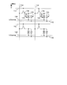
示される現フレームの画像の一部が例えば図7(2)の左欄に示されるようなものである
場合、境界検出部302によって検出される境界は、図7(2)の右欄において破線で示
される通りとなる。一方、同じ部分において1フレーム前の画像が、例えば図7(1)の
左欄に示されるようなものであった場合、保存部306から出力される境界は、図7(1
)の右欄において破線で示される通りである。
適用境界決定部308は、図7(2)の右欄で検出された境界のうち、図7(1)で示
される1フレーム前の境界から1画素分移動した部分(丸印で囲った部分)を、適用境界
として出力する。この例において、適用境界となる部分は、図7(3)の右欄で示される
ように3箇所となるので、これらを区別するため、同図で示されるように適用境界P、Q
、Rとする。
Next, a specific example of processing by the
) In the right column as indicated by a broken line.
The application
, R.
セレクター314では、適用境界に接する画素のうち、階調範囲aに属する暗画素が階
調レベルc1の映像信号に置換されるので、図7(2)の左欄で示される画像は、図7(
3)の左欄に示されるような階調レベルに補正される。詳細には、適用境界Pに対して上
側に位置する暗画素、適用境界Qに対して右側に位置する暗画素、および、適用境界Rに
対して左側に位置する暗画素が、それぞれ階調レベルc1に置換される。
また、セレクター314では、適用境界に接する画素のうち、階調範囲bに属する明画
素が階調レベルc2の映像信号に置換されるので、図7(2)の左欄で示される画像は、
図7(3)の左欄に示されるような階調レベルに補正される。詳細には、適用境界Pに対
して下側に位置する明画素、適用境界Qに対して左側に位置する明画素、および、適用境
界Rに対して右側に位置する明画素が、それぞれ階調レベルc2に置換される。
In the
The gradation level is corrected as shown in the left column of 3). Specifically, a dark pixel located on the upper side with respect to the application boundary P, a dark pixel located on the right side with respect to the application boundary Q, and a dark pixel located on the left side with respect to the application boundary R are respectively represented by gradation levels. c1 is replaced.
In the
The gradation level is corrected as shown in the left column of FIG. Specifically, a bright pixel positioned below the application boundary P, a bright pixel positioned on the left side of the application boundary Q, and a bright pixel positioned on the right side of the application boundary R Replaced with level c2.
仮に、映像信号Vid-inを映像処理回路30で処理しないで液晶パネル100に供給す
る構成としたとき、階調範囲aに属する暗画素と階調範囲bに属する明画素とにおいて、
画素電極の電位は、正極性書込であれば、図8(a)で示される通りとなる。暗画素の画
素電極の電位は、正極性書込であれば明画素の画素電極の電位よりも低くなるが、電位差
が大きいので、横電界の影響をうけやすくなる。なお、負極性であれば、電位の高低関係
が逆転するが、電位差が大きいことに変わりはないので、やはり横電界の影響をうけやす
くなる。
Assuming that the video signal Vid-in is supplied to the
In the case of positive polarity writing, the potential of the pixel electrode is as shown in FIG. The potential of the pixel electrode of the dark pixel is lower than the potential of the pixel electrode of the bright pixel in the case of positive writing, but since the potential difference is large, it is easily affected by the lateral electric field. In the case of the negative polarity, the potential level relationship is reversed, but the potential difference is still large, so that it is easily affected by the transverse electric field.
これに対して、本実施形態では、階調範囲aに属する暗画素と階調範囲bに属する明画
素とが隣接する境界から、適用境界を決定し、この適用境界に接する暗画素に対応する映
像信号Vid-outを、階調レベルc1に置換する。また、本実施形態では、この適用境界に
接する明画素に対応する映像信号Vid-outを、階調レベルc2に置換する。
このため、当該暗画素の液晶素子への印加電圧が高くなるように、換言すれば、当該暗
画素の画素電極の電位が正極性書込であれば、図8(b)で示されるように、引き上げら
れる。また、当該明画素の液晶素子への印加電圧が低くなるように、換言すれば、当該明
画素の画素電極の電位が正極性書込であれば、図8(b)で示されるように、引き下げら
れる。
On the other hand, in the present embodiment, the application boundary is determined from the boundary where the dark pixel belonging to the gradation range a and the bright pixel belonging to the gradation range b are adjacent to each other, and this corresponds to the dark pixel in contact with the application boundary. The video signal Vid-out is replaced with the gradation level c1. In the present embodiment, the video signal Vid-out corresponding to the bright pixel in contact with the application boundary is replaced with the gradation level c2.
Therefore, the voltage applied to the liquid crystal element of the dark pixel is increased, in other words, if the potential of the pixel electrode of the dark pixel is positive writing, as shown in FIG. Raised. Further, if the potential of the pixel electrode of the bright pixel is positive writing so that the voltage applied to the liquid crystal element of the bright pixel is low, in other words, as shown in FIG. Be lowered.
このため、映像信号Vid-inで示される画像が、図6(a)に示されるように、黒画素
から白画素に変化する部分が1画素ずつ移動するような場合であっても、液晶パネル10
0では、暗画素から明画素へと直接的に変化しない。つまり、図6(b)に示されるよう
に、暗画素から一旦階調レベルc1を経て、階調レベルc1の後に階調レベルc2を経て明
画素に変化する。
したがって、本実施形態では、横電界の大きさが段階的に変化して、適用境界において
大きな横電界がかかるのが防止されるので、リバースチルトドメインによる表示上の不具
合の発生を抑制することが可能となる。
Therefore, even if the image indicated by the video signal Vid-in is a case where the portion where the black pixel changes to the white pixel moves one pixel at a time as shown in FIG. 10
At 0, there is no direct change from dark pixels to bright pixels. That is, as shown in FIG. 6B, the dark pixel changes to the bright pixel once through the gradation level c1 and then after the gradation level c1 through the gradation level c2.
Therefore, in this embodiment, since the magnitude of the lateral electric field changes stepwise and a large lateral electric field is prevented from being applied at the application boundary, it is possible to suppress the occurrence of display defects due to the reverse tilt domain. It becomes possible.
また、本実施形態において、適用境界は、映像信号Vid-inで示される現フレームの画
像において、階調範囲aに属する暗画素と階調範囲bに属する明画素とが隣接する境界の
うち、前フレームの境界から1画素分移動した部分のみとしている。このため、本実施形
態では、元の映像信号Vid-inで指定される階調レベルをそれとは異なる階調レベルc1や
階調レベルc2に置換する画素(表示背反画素)については、単に現フレームにおいて境
界に接する画素を補正(置換)対象とする構成と比較して、少なく抑えられる。
In the present embodiment, the application boundary is the boundary between the dark pixel belonging to the gradation range a and the bright pixel belonging to the gradation range b in the image of the current frame indicated by the video signal Vid-in. Only the portion moved by one pixel from the boundary of the previous frame is shown. For this reason, in this embodiment, a pixel (display anti-pixel) that replaces the gradation level specified by the original video signal Vid-in with a gradation level c1 or gradation level c2 different from the gradation level is simply the current frame. As compared with the configuration in which the pixels in contact with the boundary in FIG.
このように、本実施形態によれば、上述したリバースチルトドメインに起因する表示上
の不具合の発生を事前に回避することが可能となる。さらに、映像信号Vid-inで規定さ
れる画像のうち、適用境界に接する画素の階調レベルが局所的に置換されるので、当該置
換による表示画像の変更がユーザーに知覚される可能性も小さい。くわえて、本実施形態
では、液晶パネル100の構造を変更する必要がないので、開口率の低下を招くこともな
いし、また、構造を工夫しないで既に製作された液晶パネルに適用することも可能である
。
As described above, according to the present embodiment, it is possible to avoid in advance the occurrence of display defects due to the above-described reverse tilt domain. Further, among the images defined by the video signal Vid-in, since the gradation level of the pixel in contact with the application boundary is locally replaced, the possibility that the change of the display image due to the replacement is perceived by the user is small. . In addition, in this embodiment, since it is not necessary to change the structure of the
<実施形態の応用・変形例>
上述した実施形態では、種々の応用・変形が可能である。以下、応用・変形例について
説明する。
<Application and modification of embodiment>
In the above-described embodiment, various applications and modifications are possible. Hereinafter, applications and modifications will be described.
<その1:置換する画素数>
上述した実施形態では、適用境界に接する一つの暗画素を階調レベルc1に置換する構
成であった。このような構成において、暗画素と明画素との適用境界で生じる横電界を小
さくする、という観点からすると、適用境界に接する暗画素への印加電圧の引き上げ量を
大きくすることが好ましい。ただし、印加電圧の引き上げ量(補正量)を大きくする、と
いうことは、それだけ、元画像から乖離し、表示背反となることを意味する。
そこで、暗画素が連続するような場合には、適用境界に接する暗画素に加え、当該暗画
素に対して適用境界から離れる方向(適用境界に直交する方向)に連続するK(Kは1以
上の整数)個の暗画素についても階調レベルを置換し、適用境界に接する明画素について
は、適用境界に接する明画素のみを階調レベルc2に置換する構成としてもよい。
このためには、判別部310が、次のような場合にデータQの値を「1」で出力すれば
よい。詳細には、適用境界から離れる方向の画素であって映像信号Vid-dで示される画素
の階調レベルが階調範囲aに属し、適用境界から当該画素までが階調範囲aで連続し、適
用境界から当該画素までの距離が(K+1)画素以内である場合に、データQの値を「1
」で出力すればよい。なお、置換候補とする画素数については、適用境界に接する画素を
含めて2〜10個程度が好ましい。
<Part 1: Number of pixels to be replaced>
In the above-described embodiment, one dark pixel in contact with the application boundary is replaced with the gradation level c1. In such a configuration, from the viewpoint of reducing the lateral electric field generated at the application boundary between the dark pixel and the light pixel, it is preferable to increase the amount of voltage applied to the dark pixel in contact with the application boundary. However, increasing the amount of increase (correction amount) of the applied voltage means that the display image is far from the original image.
Therefore, in the case where the dark pixels are continuous, in addition to the dark pixels that are in contact with the application boundary, K that is continuous in the direction away from the application boundary (direction orthogonal to the application boundary) with respect to the dark pixel (K is 1 or more) The gradation level may also be replaced with respect to the number of dark pixels, and with respect to the bright pixel in contact with the application boundary, only the bright pixel in contact with the application boundary may be replaced with the gradation level c2.
For this purpose, the
”. In addition, about the number of pixels made into a replacement candidate, about 2-10 pieces including the pixel which touches an application boundary are preferable.
図9は、適用境界に接する暗画素と、当該暗画素に隣接する1つの暗画素との計2画素
について階調レベルを置換する場合の処理例を示す図である。前フレームおよび現フレー
ムの画像と、検出される境界および適用境界とついては、図7の例と同様であるが、本例
では、適用境界Pから上方向に2画素以内で位置する暗画素がそれぞれ階調レベルc1に
置換される。すなわち、適用境界Pに接する暗画素に加え、当該暗画素に上方向で隣接す
る暗画素の計2画素が、それぞれ階調レベルc1に置換される。同様に、適用境界Qに対
して接する暗画素に加え、左方向に隣接する暗画素の計2画素が、それぞれ階調レベルc
1に置換される。ただし、適用境界Rに接する暗画素は右方向に連続していないので、適
用境界Rに接する暗画素のみが階調レベルc1に置換される。
このように適用境界に接する画素と、当該画素に対して適用境界から離れる方向に隣接
する1以上の画素についても階調レベルを置換する構成にすると、補正量を大きくしなく
ても、横電界を小さくすることが可能となる。
FIG. 9 is a diagram illustrating a processing example in the case where the gradation level is replaced for a total of two pixels, that is, a dark pixel that is in contact with the application boundary and a single dark pixel adjacent to the dark pixel. The images of the previous frame and the current frame, the detected boundary, and the application boundary are the same as in the example of FIG. 7, but in this example, dark pixels located within two pixels upward from the application boundary P are respectively It is replaced with the gradation level c1. That is, in addition to the dark pixels in contact with the application boundary P, a total of two pixels, the dark pixels adjacent to the dark pixels in the upward direction, are each replaced with the gradation level c1. Similarly, in addition to the dark pixels that are in contact with the application boundary Q, a total of two pixels, that is, dark pixels adjacent in the left direction, respectively have gradation levels c
Replaced with 1. However, since the dark pixels in contact with the application boundary R are not continuous in the right direction, only the dark pixels in contact with the application boundary R are replaced with the gradation level c1.
In this way, if the pixel is in contact with the application boundary and at least one pixel adjacent to the pixel in the direction away from the application boundary, the gray level is replaced, the lateral electric field can be increased without increasing the correction amount. Can be reduced.
なお、適用境界に接する暗画素と、当該暗画素に対して適用境界から離れる方向に連続
するK個の暗画素について階調レベルを置換する構成においては、図10に示したように
、適用境界に接する明画素と、当該明画素に対して適用境界から離れる方向に連続するK
個の明画素についても階調レベルを置換する構成としてもよい。
この構成の場合、判別部310は、映像信号Vid-dで示される画素の階調レベルが階調
範囲bに属し、適用境界から当該画素までが階調範囲bで連続し、適用境界から当該画素
までの距離が(K+1)画素以内である場合に、データQの値を「2」で出力すればよい
。
また、適用境界に接する明画素と、当該明画素に対して適用境界から離れる方向に連続
するK個の明画素に階調レベルを置換する構成においては、適用境界に接する暗画素につ
いてのみ階調レベルc1に置換する構成としてもよい。
In the configuration in which the gradation level is replaced for a dark pixel in contact with the application boundary and K dark pixels continuous in a direction away from the application boundary with respect to the dark pixel, as illustrated in FIG. A bright pixel that touches the pixel and K that continues in a direction away from the application boundary with respect to the bright pixel.
A configuration may be adopted in which the gradation levels are also replaced for the individual bright pixels.
In the case of this configuration, the
Further, in the configuration in which the gradation level is replaced with a bright pixel that is in contact with the application boundary and K bright pixels that are continuous in a direction away from the application boundary with respect to the bright pixel, gradation is applied only to the dark pixels that are in contact with the application boundary. A configuration may be adopted in which the level is replaced with c1.
<その2:適用境界のさらなる絞り込み>
実施形態では、階調範囲aの暗画素と階調範囲bの明画素とが隣接する境界を検出し、
その検出した境界のうち、1フレーム前の境界から1画素分だけ移動したものを適用境界
とした。このような適用境界については、前フレームから現フレームへの変化を考えたと
きに、次の3パターンが考えられる。すなわち、現フレームにおいて暗画素と明画素とが
隣接する場合に、前フレームでは、その2つがともに暗画素であった場合(パターン1)
、ともに明画素であった場合(パターン2)、前フレームでは明画素と暗画素であって、
現フレームにおいて入れ替わった場合(パターン3)の3つが考えられる。
リバースチルトドメインは、図6(a)で説明したように、また、上記条件(3)から
推察されるように、前フレームで暗画素と明画素とが隣接したときに、印加電圧が低い方
の画素(液晶分子が不安定な状態にある画素)が、現フレームにおいて印加電圧が高い方
向に変化するときに発生しやすい。
したがって、上述した実施形態において決定した適用境界から、パターン2を排除して
も影響が少ないことが判る。パターン2は、前フレームにおいて2つの画素がともに液晶
分子が安定状態にある明画素であり、それが画像パターンの動きによって、いずれか一方
が暗画素に変化する場合であるから、いずれの2画素においてもリバースチルトドメイン
が発生しにくい状況にある、ということができるためである。
<Part 2: Further narrowing down application boundaries>
In the embodiment, a boundary where a dark pixel in the gradation range a and a bright pixel in the gradation range b are adjacent to each other is detected.
Among the detected boundaries, a boundary that is moved by one pixel from the boundary one frame before is defined as an application boundary. Regarding such an application boundary, the following three patterns can be considered when considering a change from the previous frame to the current frame. That is, when a dark pixel and a bright pixel are adjacent to each other in the current frame, both of them are dark pixels in the previous frame (pattern 1).
If both are bright pixels (pattern 2), the previous frame is a bright pixel and a dark pixel,
There are three possible cases where the current frame is replaced (pattern 3).
The reverse tilt domain has a lower applied voltage when dark pixels and bright pixels are adjacent to each other in the previous frame, as described in FIG. Are likely to occur when the applied voltage changes in the higher direction in the current frame.
Therefore, it can be seen that even if the pattern 2 is excluded from the application boundary determined in the above-described embodiment, the influence is small. Pattern 2 is a case where both of the two pixels in the previous frame are bright pixels in which the liquid crystal molecules are in a stable state, and one of the two pixels changes to a dark pixel due to the movement of the image pattern. This is because the reverse tilt domain is unlikely to occur.
実施形態において適用境界決定部308は、現フレームにおいて暗画素と明画素とが隣
接する境界を検出し、該検出した境界のうち、1フレーム前の境界から1画素分だけ移動
したものを適用境界として決定する構成としたが、適用境界を決定する際に、現フレーム
における暗画素と明画素とが前フレームにおいていずれも明画素であったときには、適用
境界として決定しない構成とすれば、パターン2の画素が、補正対象から除外されること
になる。
In the embodiment, the application
図11は、適用境界から上記パターン2を除外する場合の処理例を示す図である。前フ
レームおよび現フレームの画像と、検出される境界については、図7の例と同様である。
図7の例では、P、Q、Rがいずれも適用境界として決定されたが、このうち、本例では
、Rを挟む2つの画素が前フレームにおいていずれも明画素であるから、補正対象から除
外される。
このようにパターン2を除外すると、表示背反となる画素をさらに少なくすることが可
能となる。なお、パターン2については、見方を変えると、明画素(電圧の高い方の画素
)からなるパターンが暗画素(電圧の低い方の画素)からなるパターンに向かって移動し
たとき、と言い換えることもできる。
FIG. 11 is a diagram illustrating a processing example when the pattern 2 is excluded from the application boundary. The images of the previous frame and the current frame and the detected boundary are the same as in the example of FIG.
In the example of FIG. 7, P, Q, and R are all determined as application boundaries. However, in this example, two pixels sandwiching R are both bright pixels in the previous frame. Excluded.
If the pattern 2 is excluded in this way, it is possible to further reduce the number of pixels that are contradictory to each other. In terms of the pattern 2, in other words, it can be rephrased when the pattern composed of bright pixels (pixels with higher voltage) moves toward the pattern composed of dark pixels (pixels with lower voltage). it can.
<その3:ノーマリーホワイトモード>
本実施形態において、液晶105をVA方式としたノーマリーブラックモードとして説
明したが、液晶105を例えばTN方式として、電圧無印加時において液晶素子120が
白状態となるノーマリーホワイトモードとしてもよい。
ノーマリーホワイトモードとしたとき、液晶素子120の印加電圧と透過率との関係は
、図4の(b)に示されるようなV−T特性で表され、印加電圧が高くなるにつれて透過
率が減少する。横電界の影響を受けやすい画素は、印加電圧が低い方の画素であることに
変わりはないが、ノーマリーホワイトモードにおいて印加電圧が低い方の画素は明画素と
なる。
このため、ノーマリーホワイトモードにおいて、映像処理回路30は、印加電圧が電圧
範囲Aに属する明画素と電圧範囲Bに属する暗画素とが隣接する境界から、適用境界を決
定する。また、映像回路30は、ノーマリーホワイトモードにおいて、適用境界に接する
明画素に対応する映像信号Vid-outを、電圧範囲Aに相当する階調レベルよりも暗い階調
レベルc1に置換する処理をする。
また、映像回路30は、ノーマリーホワイトモードにおいて、適用境界に接する暗画素
に対応する映像信号Vid-outを、電圧範囲Bに相当する階調レベルよりも明るい階調レベ
ルc2に置換する処理をする。なお、ノーマリーブラックモードと同様に複数画素につい
て階調レベルを置換するようにしてもよい。
<Part 3: Normally White Mode>
In the present embodiment, the
In the normally white mode, the relationship between the applied voltage and the transmittance of the
For this reason, in the normally white mode, the
Further, the
上述した各実施形態において、映像信号Vid-inは、画素の階調レベルを指定するもの
としたが、液晶素子の印加電圧を直接的に指定するものとしても良い。映像信号Vid- in
が液晶素子の印加電圧を指定する場合、指定される印加電圧によって境界を判別して、電
圧を補正する構成とすれば良い。
In each of the embodiments described above, the video signal Vid-in designates the gradation level of the pixel, but it may also designate the voltage applied to the liquid crystal element directly. Video signal Vid-in
When the applied voltage of the liquid crystal element is designated, the boundary may be determined by the designated applied voltage to correct the voltage.
<電子機器>
次に、上述した実施形態に係る液晶表示装置を用いた電子機器の一例として、液晶パネ
ル100をライトバルブとして用いた投射型表示装置(プロジェクター)について説明す
る。図12は、このプロジェクターの構成を示す平面図である。
この図に示されるように、プロジェクター2100の内部には、ハロゲンランプ等の白
色光源からなるランプユニット2102が設けられている。このランプユニット2102
から射出された投射光は、内部に配置された3枚のミラー2106および2枚のダイクロ
イックミラー2108によってR(赤)色、G(緑)色、B(青)色の3原色に分離され
て、各原色に対応するライトバルブ100R、100Gおよび100Bにそれぞれ導かれ
る。なお、B色の光は、他のR色やG色と比較すると、光路が長いので、その損失を防ぐ
ために、入射レンズ2122、リレーレンズ2123および出射レンズ2124からなる
リレーレンズ系2121を介して導かれる。
<Electronic equipment>
Next, a projection display device (projector) using the
As shown in this figure, a
The projection light emitted from the light is separated into three primary colors of R (red), G (green), and B (blue) by three
このプロジェクター2100では、液晶パネル100を含む液晶表示装置が、R色、G
色、B色のそれぞれに対応して3組設けられる。ライトバルブ100R、100Gおよび
100Bの構成は、上述した液晶パネル100と同様である。R色、G色、B色のそれぞ
れの原色成分の階調レベルを指定するに映像信号がそれぞれ外部上位回路から供給されて
、ライトバルブ100R、100Gおよび100がそれぞれ駆動される構成となっている
。
ライトバルブ100R、100G、100Bによってそれぞれ変調された光は、ダイク
ロイックプリズム2112に3方向から入射する。そして、このダイクロイックプリズム
2112において、R色およびB色の光は90度に屈折する一方、G色の光は直進する。
したがって、各原色の画像が合成された後、スクリーン2120には、投射レンズ211
4によってカラー画像が投射されることとなる。
In the
Three sets are provided corresponding to each of the color and the B color. The configuration of the
The lights modulated by the
Therefore, after the images of the respective primary colors are combined, the projection lens 211 is displayed on the
4 will project a color image.
なお、ライトバルブ100R、100Gおよび100Bには、ダイクロイックミラー2
108によって、R、G、Bの各原色に対応する光が入射するので、カラーフィルタを設
ける必要はない。また、ライトバルブ100R、100Bの透過像は、ダイクロイックプ
リズム2112により反射した後に投射されるのに対し、ライトバルブ100Gの透過像
はそのまま投射されるので、ライトバルブ100R、100Bによる水平走査方向は、ラ
イトバルブ100Gによる水平走査方向と逆向きにして、水平方向の左右を反転させた像
を表示する構成となっている。
The
Since light corresponding to the primary colors of R, G, and B is incident by 108, there is no need to provide a color filter. In addition, the transmission images of the
液晶パネル100をライトバルブに用いる例としては、図12を参照して説明したプロ
ジェクターの他にも、リヤ・プロジェクション型のテレビジョンが挙げられる。また、液
晶パネル100については、ミラーレスのレンズ交換式のデジタルカメラや、ビデオカメ
ラなどにおける電子ビューファインダー(EVF)にも適用可能である。
このほかにも、適用可能な電子機器として、ヘッドマウントディスプレイや、カーナビ
ゲーション装置、ページャー、電子手帳、電卓、ワードプロセッサー、ワークステーショ
ン、テレビ電話、POS端末、デジタルスチルカメラ、携帯電話機、タッチパネルを備え
た機器等などが挙げられる。そして、これらの各種の電子機器に対して、上記液晶表示装
置が適用可能なのは言うまでもない。
As an example of using the
Other applicable electronic devices include a head mounted display, car navigation device, pager, electronic notebook, calculator, word processor, workstation, videophone, POS terminal, digital still camera, mobile phone, and touch panel. Equipment etc. are mentioned. Needless to say, the liquid crystal display device can be applied to these various electronic devices.
1・・・液晶表示装置、30・・・映像処理回路、100・・・液晶パネル、100a・
・・素子基板、100b・・・対向基板、105・・・液晶、108・・・コモン電極、
118・・・画素電極、120・・・液晶素子、300・・・補正部、302・・・境界
検出部、308・・・適用境界決定部、310・・・判別部、314・・・セレクター、
316・・・D/A変換器、2100・・・プロジェクター
DESCRIPTION OF
..Element substrate, 100b ... opposite substrate, 105 ... liquid crystal, 108 ... common electrode,
118 ... Pixel electrode, 120 ... Liquid crystal element, 300 ... Correction unit, 302 ... Boundary detection unit, 308 ... Application boundary determination unit, 310 ... Discrimination unit, 314 ... Selector ,
316 ... D / A converter, 2100 ... Projector
Claims (7)
入力された映像信号で指定される印加電圧が第1電圧を下回る第1画素と、前記印加電圧が前記第1電圧よりも大きい第2電圧以上である第2画素との境界を、現フレームおよび前記現フレームより一つ前の前フレームでそれぞれ検出する境界検出部と、
前記現フレームの境界において前記前フレームの境界から1画素分だけ離れた境界部分に接する前記第1画素および前記第2画素に対応する液晶素子への印加電圧を指定する映像信号を、前記第1画素および前記第2画素で生じる横電界を低減する方向に補正する補正部と、
を備えることを特徴とする映像処理回路。 A video processing circuit that inputs a video signal designating an applied voltage of a liquid crystal element for each pixel and defines an applied voltage of the liquid crystal element based on the corrected video signal,
The boundary between the first pixel whose applied voltage specified by the input video signal is lower than the first voltage and the second pixel whose applied voltage is greater than or equal to the second voltage greater than the first voltage is defined as the current frame and a boundary detecting unit for detecting respectively the previous frame of one before the current frame,
A video signal designating an applied voltage to the liquid crystal element corresponding to the first pixel and the second pixel adjacent to the boundary from one pixel apart boundary portion of the front frame at the border of the current frame, the first a correcting unit for correcting the direction to reduce the transverse electric field generated by the pixel and the second pixel,
A video processing circuit comprising:
前記境界部分に接する前記第1画素から前記境界部分の反対側へ連続する1以上の予め定められた個数の前記第1画素に対応する液晶素子への印加電圧を指定する映像信号を、前記横電界を低減する方向に補正する
ことを特徴とする請求項1に記載の映像処理回路。 The correction unit is
A video signal designating an applied voltage to the liquid crystal element corresponding to one or more of the first pixel of the predetermined number of consecutive to the opposite side of the boundary from the first pixel adjacent to the boundary, the lateral The video processing circuit according to claim 1, wherein correction is performed in a direction in which the electric field is reduced.
前記境界部分に接する前記第2画素から前記境界部分の反対側へ連続する1以上の予め定められた個数の前記第2画素に対応する液晶素子への印加電圧を指定する映像信号を、前記横電界を低減する方向に補正する
ことを特徴とする請求項1または請求項2に記載の映像処理回路。 The correction unit is
A video signal designating an applied voltage to the liquid crystal element corresponding to the second pixel of one or more predetermined number of consecutive to the opposite side of the boundary from the second pixel adjacent to the boundary, the lateral The video processing circuit according to claim 1, wherein correction is performed in a direction in which the electric field is reduced.
前記境界部分に接する前記第1画素および前記第2画素が、前記前フレームにおいていずれも前記第2画素であった場合には、前記境界部分を挟んだ位置にある前記第1画素および前記第2画素を補正対象から除外する
ことを特徴とする請求項1に記載の映像処理回路。 The correction unit is
Wherein the first pixel and the second pixel adjacent to the boundary portion, the front when were both the second pixel in the frame, the first pixel and the second in a position sandwiching the boundary portion The video processing circuit according to claim 1, wherein pixels are excluded from correction targets.
入力された映像信号で指定される印加電圧が第1電圧を下回る第1画素と、前記印加電圧が前記第1電圧よりも大きい第2電圧以上である第2画素との境界を、現フレームおよび前記現フレームより一つ前の前フレームでそれぞれ検出し、
前記現フレームの境界において前記前フレームの境界から1画素分だけ離れた境界部分に接する前記第1画素および前記第2画素に対応する液晶素子への印加電圧を指定する映像信号を、前記第1画素および前記第2画素で生じる横電界を低減する方向に補正する
ことを特徴とする映像処理方法。 A video processing circuit that corrects a video signal designating an applied voltage of a liquid crystal element for each pixel and defines an applied voltage of the liquid crystal element based on the corrected video signal,
The boundary between the first pixel whose applied voltage specified by the input video signal is lower than the first voltage and the second pixel whose applied voltage is greater than or equal to the second voltage greater than the first voltage is defined as the current frame and the detected respectively preceding the previous frame than the current frame,
A video signal designating an applied voltage to the liquid crystal element corresponding to the first pixel and the second pixel adjacent to the boundary from one pixel apart boundary portion of the front frame at the border of the current frame, the first image processing method and correcting the direction to reduce the transverse electric field generated by the pixel and the second pixel.
画素毎に前記液晶素子の印加電圧を指定する映像信号が入力されるとともに、補正した映像信号に基づいて前記液晶素子の印加電圧をそれぞれ規定する映像処理回路とを、有し、
前記映像処理回路は、
入力された映像信号で指定される印加電圧が第1電圧を下回る第1画素と、前記印加電圧が前記第1電圧よりも大きい第2電圧以上である第2画素との境界を、現フレームおよび前記現フレームより一つ前の前フレームでそれぞれ検出する境界検出部と、
前記現フレームの境界において前記前フレームの境界から1画素分だけ離れた境界部分に接する前記第1画素および前記第2画素に対応する液晶素子への印加電圧を指定する映像信号を、前記第1画素および前記第2画素で生じる横電界を低減する方向に補正する補正部と、
を備えることを特徴とする液晶表示装置。 A liquid crystal panel having a liquid crystal element in which a liquid crystal is sandwiched between a pixel electrode provided corresponding to each of the plurality of pixels on the first substrate and a common electrode provided on the second substrate;
A video signal that specifies an applied voltage of the liquid crystal element for each pixel, and a video processing circuit that defines an applied voltage of the liquid crystal element based on the corrected video signal,
The video processing circuit includes:
The boundary between the first pixel whose applied voltage specified by the input video signal is lower than the first voltage and the second pixel whose applied voltage is greater than or equal to the second voltage greater than the first voltage is defined as the current frame and a boundary detecting unit for detecting respectively the previous frame of one before the current frame,
A video signal designating an applied voltage to the liquid crystal element corresponding to the first pixel and the second pixel adjacent to the boundary from one pixel apart boundary portion of the front frame at the border of the current frame, the first a correcting unit for correcting the direction to reduce the transverse electric field generated by the pixel and the second pixel,
A liquid crystal display device comprising:
Priority Applications (3)
| Application Number | Priority Date | Filing Date | Title |
|---|---|---|---|
| JP2010039794A JP5370214B2 (en) | 2010-02-25 | 2010-02-25 | Video processing circuit, video processing method, liquid crystal display device, and electronic apparatus |
| US13/022,138 US8497829B2 (en) | 2010-02-25 | 2011-02-07 | Video processing circuit, liquid crystal display device, electronic apparatus, and video processing method |
| CN2011100461377A CN102169678A (en) | 2010-02-25 | 2011-02-25 | Video processing circuit, video processing method, liquid crystal display device and electronic apparatus |
Applications Claiming Priority (1)
| Application Number | Priority Date | Filing Date | Title |
|---|---|---|---|
| JP2010039794A JP5370214B2 (en) | 2010-02-25 | 2010-02-25 | Video processing circuit, video processing method, liquid crystal display device, and electronic apparatus |
Publications (2)
| Publication Number | Publication Date |
|---|---|
| JP2011175136A JP2011175136A (en) | 2011-09-08 |
| JP5370214B2 true JP5370214B2 (en) | 2013-12-18 |
Family
ID=44476114
Family Applications (1)
| Application Number | Title | Priority Date | Filing Date |
|---|---|---|---|
| JP2010039794A Active JP5370214B2 (en) | 2010-02-25 | 2010-02-25 | Video processing circuit, video processing method, liquid crystal display device, and electronic apparatus |
Country Status (3)
| Country | Link |
|---|---|
| US (1) | US8497829B2 (en) |
| JP (1) | JP5370214B2 (en) |
| CN (1) | CN102169678A (en) |
Families Citing this family (12)
| Publication number | Priority date | Publication date | Assignee | Title |
|---|---|---|---|---|
| JP5556234B2 (en) * | 2010-02-25 | 2014-07-23 | セイコーエプソン株式会社 | VIDEO PROCESSING CIRCUIT, ITS PROCESSING METHOD, LIQUID CRYSTAL DISPLAY DEVICE, AND ELECTRONIC DEVICE |
| JP5720221B2 (en) * | 2010-12-13 | 2015-05-20 | セイコーエプソン株式会社 | Video processing method, video processing circuit, liquid crystal display device, and electronic apparatus |
| JP5707973B2 (en) | 2011-01-27 | 2015-04-30 | セイコーエプソン株式会社 | Video processing method, video processing circuit, liquid crystal display device, and electronic apparatus |
| JP6083111B2 (en) * | 2012-01-30 | 2017-02-22 | セイコーエプソン株式会社 | Video processing circuit, video processing method, liquid crystal display device, and electronic apparatus |
| JP6010921B2 (en) * | 2012-02-20 | 2016-10-19 | セイコーエプソン株式会社 | Electro-optical device control method, electro-optical device control device, electro-optical device, and electronic apparatus |
| JP5903954B2 (en) | 2012-03-15 | 2016-04-13 | セイコーエプソン株式会社 | VIDEO PROCESSING CIRCUIT, VIDEO PROCESSING METHOD, AND ELECTRONIC DEVICE |
| JP6078959B2 (en) | 2012-03-16 | 2017-02-15 | セイコーエプソン株式会社 | VIDEO PROCESSING CIRCUIT, VIDEO PROCESSING METHOD, AND ELECTRONIC DEVICE |
| JP6078965B2 (en) | 2012-03-27 | 2017-02-15 | セイコーエプソン株式会社 | Video processing circuit, video processing method, and electronic device |
| JP5929538B2 (en) * | 2012-06-18 | 2016-06-08 | セイコーエプソン株式会社 | Display control circuit, display control method, electro-optical device, and electronic apparatus |
| JP6080459B2 (en) * | 2012-09-28 | 2017-02-15 | キヤノン株式会社 | Image processing apparatus, image processing method, and program |
| US11545100B2 (en) * | 2021-03-09 | 2023-01-03 | Sharp Kabushiki Kaisha | Liquid crystal display apparatus |
| CN115512667B (en) * | 2022-10-18 | 2024-01-12 | 重庆惠科金渝光电科技有限公司 | Driving method of electronic paper equipment and electronic paper equipment |
Family Cites Families (18)
| Publication number | Priority date | Publication date | Assignee | Title |
|---|---|---|---|---|
| JP2761128B2 (en) * | 1990-10-31 | 1998-06-04 | 富士通株式会社 | Liquid crystal display |
| JP3135689B2 (en) | 1992-07-20 | 2001-02-19 | 株式会社東芝 | Active matrix type liquid crystal display |
| JP2003172915A (en) * | 2001-09-26 | 2003-06-20 | Sharp Corp | Liquid crystal display device |
| JP4846571B2 (en) * | 2003-04-24 | 2011-12-28 | ディスプレイテック,インコーポレイテッド | Microdisplay system and image display method |
| JP4817000B2 (en) * | 2003-07-04 | 2011-11-16 | ソニー株式会社 | Image processing apparatus and method, and program |
| JP4197322B2 (en) * | 2004-01-21 | 2008-12-17 | シャープ株式会社 | Display device, liquid crystal monitor, liquid crystal television receiver and display method |
| KR100588132B1 (en) * | 2004-10-04 | 2006-06-09 | 삼성전자주식회사 | Display device |
| JP2006330171A (en) * | 2005-05-24 | 2006-12-07 | Sharp Corp | Liquid crystal display device |
| US8212755B2 (en) * | 2005-05-24 | 2012-07-03 | Sharp Kabushiki Kaisha | Liquid crystal display device and driving method of the same |
| KR100739735B1 (en) * | 2005-09-16 | 2007-07-13 | 삼성전자주식회사 | Liquid crystal display driving method and apparatus using the same |
| US20080018630A1 (en) * | 2006-07-18 | 2008-01-24 | Yusuke Fujino | Liquid crystal display device, liquid crystal display and method of driving liquid crystal display device |
| CN101192386A (en) * | 2006-11-27 | 2008-06-04 | 联詠科技股份有限公司 | Method for driving liquid crystal display and related device |
| JP2008256954A (en) * | 2007-04-05 | 2008-10-23 | Hitachi Displays Ltd | Display device |
| WO2009031391A1 (en) * | 2007-09-07 | 2009-03-12 | Sharp Kabushiki Kaisha | Method for driving liquid crystal display device and liquid crystal display device |
| JP2009069608A (en) | 2007-09-14 | 2009-04-02 | Sanyo Electric Co Ltd | Liquid crystal projector |
| US20090153743A1 (en) | 2007-12-18 | 2009-06-18 | Sony Corporation | Image processing device, image display system, image processing method and program therefor |
| JP4661965B2 (en) * | 2009-02-18 | 2011-03-30 | ソニー株式会社 | Liquid crystal display device |
| JP5370169B2 (en) | 2010-01-15 | 2013-12-18 | セイコーエプソン株式会社 | VIDEO PROCESSING CIRCUIT, ITS PROCESSING METHOD, LIQUID CRYSTAL DISPLAY DEVICE, AND ELECTRONIC DEVICE |
-
2010
- 2010-02-25 JP JP2010039794A patent/JP5370214B2/en active Active
-
2011
- 2011-02-07 US US13/022,138 patent/US8497829B2/en active Active
- 2011-02-25 CN CN2011100461377A patent/CN102169678A/en active Pending
Also Published As
| Publication number | Publication date |
|---|---|
| JP2011175136A (en) | 2011-09-08 |
| CN102169678A (en) | 2011-08-31 |
| US8497829B2 (en) | 2013-07-30 |
| US20110205207A1 (en) | 2011-08-25 |
Similar Documents
| Publication | Publication Date | Title |
|---|---|---|
| JP5370169B2 (en) | VIDEO PROCESSING CIRCUIT, ITS PROCESSING METHOD, LIQUID CRYSTAL DISPLAY DEVICE, AND ELECTRONIC DEVICE | |
| JP5370214B2 (en) | Video processing circuit, video processing method, liquid crystal display device, and electronic apparatus | |
| JP5229162B2 (en) | VIDEO PROCESSING CIRCUIT, ITS PROCESSING METHOD, LIQUID CRYSTAL DISPLAY DEVICE, AND ELECTRONIC DEVICE | |
| JP5381807B2 (en) | VIDEO PROCESSING CIRCUIT, ITS PROCESSING METHOD, LIQUID CRYSTAL DISPLAY DEVICE, AND ELECTRONIC DEVICE | |
| JP5598014B2 (en) | VIDEO PROCESSING CIRCUIT, ITS PROCESSING METHOD, LIQUID CRYSTAL DISPLAY DEVICE, AND ELECTRONIC DEVICE | |
| JP5233920B2 (en) | VIDEO PROCESSING CIRCUIT, ITS PROCESSING METHOD, LIQUID CRYSTAL DISPLAY DEVICE, AND ELECTRONIC DEVICE | |
| JP5707973B2 (en) | Video processing method, video processing circuit, liquid crystal display device, and electronic apparatus | |
| JP5556234B2 (en) | VIDEO PROCESSING CIRCUIT, ITS PROCESSING METHOD, LIQUID CRYSTAL DISPLAY DEVICE, AND ELECTRONIC DEVICE | |
| JP5304684B2 (en) | VIDEO PROCESSING CIRCUIT, ITS PROCESSING METHOD, LIQUID CRYSTAL DISPLAY DEVICE, AND ELECTRONIC DEVICE | |
| JP5720221B2 (en) | Video processing method, video processing circuit, liquid crystal display device, and electronic apparatus | |
| JP5304669B2 (en) | VIDEO PROCESSING CIRCUIT, ITS PROCESSING METHOD, LIQUID CRYSTAL DISPLAY DEVICE, AND ELECTRONIC DEVICE | |
| JP5454092B2 (en) | VIDEO PROCESSING CIRCUIT, ITS PROCESSING METHOD, LIQUID CRYSTAL DISPLAY DEVICE, AND ELECTRONIC DEVICE | |
| JP5381804B2 (en) | Video processing circuit, video processing method, liquid crystal display device, and electronic apparatus | |
| JP6078965B2 (en) | Video processing circuit, video processing method, and electronic device | |
| JP2012242798A (en) | Correction voltage setup method, video processing method, correction voltage setup device, video processing circuit, liquid crystal display device, and electronic apparatus | |
| JP5601173B2 (en) | Video processing method, video processing circuit, liquid crystal display device, and electronic apparatus | |
| JP2012242797A (en) | Video processing method, video processing circuit, liquid crystal display device, and electronic apparatus | |
| JP6083111B2 (en) | Video processing circuit, video processing method, liquid crystal display device, and electronic apparatus | |
| JP2012168229A (en) | Video processing method, video processing circuit, liquid crystal display device and electronic apparatus | |
| JP5574000B2 (en) | Signal processing device, liquid crystal display device, electronic device, and signal processing method | |
| JP5510580B2 (en) | Signal processing device, signal processing method, liquid crystal display device, and electronic apparatus | |
| JP2014219686A (en) | Video processing circuit, processing method of the same, liquid crystal display device, and electronic apparatus |
Legal Events
| Date | Code | Title | Description |
|---|---|---|---|
| A621 | Written request for application examination |
Free format text: JAPANESE INTERMEDIATE CODE: A621 Effective date: 20130130 |
|
| A977 | Report on retrieval |
Free format text: JAPANESE INTERMEDIATE CODE: A971007 Effective date: 20130513 |
|
| A131 | Notification of reasons for refusal |
Free format text: JAPANESE INTERMEDIATE CODE: A131 Effective date: 20130521 |
|
| A977 | Report on retrieval |
Free format text: JAPANESE INTERMEDIATE CODE: A971007 Effective date: 20130704 |
|
| A521 | Written amendment |
Free format text: JAPANESE INTERMEDIATE CODE: A523 Effective date: 20130719 |
|
| TRDD | Decision of grant or rejection written | ||
| A01 | Written decision to grant a patent or to grant a registration (utility model) |
Free format text: JAPANESE INTERMEDIATE CODE: A01 Effective date: 20130820 |
|
| A61 | First payment of annual fees (during grant procedure) |
Free format text: JAPANESE INTERMEDIATE CODE: A61 Effective date: 20130902 |
|
| R150 | Certificate of patent or registration of utility model |
Ref document number: 5370214 Country of ref document: JP Free format text: JAPANESE INTERMEDIATE CODE: R150 Free format text: JAPANESE INTERMEDIATE CODE: R150 |
|
| S531 | Written request for registration of change of domicile |
Free format text: JAPANESE INTERMEDIATE CODE: R313531 |
|
| R350 | Written notification of registration of transfer |
Free format text: JAPANESE INTERMEDIATE CODE: R350 |