JP5368562B2 - Lighting device and display device - Google Patents
Lighting device and display device Download PDFInfo
- Publication number
- JP5368562B2 JP5368562B2 JP2011523579A JP2011523579A JP5368562B2 JP 5368562 B2 JP5368562 B2 JP 5368562B2 JP 2011523579 A JP2011523579 A JP 2011523579A JP 2011523579 A JP2011523579 A JP 2011523579A JP 5368562 B2 JP5368562 B2 JP 5368562B2
- Authority
- JP
- Japan
- Prior art keywords
- light
- light emitting
- guide plate
- light guide
- emitting diode
- Prior art date
- Legal status (The legal status is an assumption and is not a legal conclusion. Google has not performed a legal analysis and makes no representation as to the accuracy of the status listed.)
- Expired - Fee Related
Links
- 239000000758 substrate Substances 0.000 claims description 56
- 238000005286 illumination Methods 0.000 claims description 40
- 239000004973 liquid crystal related substance Substances 0.000 description 53
- 239000011159 matrix material Substances 0.000 description 8
- 238000005452 bending Methods 0.000 description 6
- 238000010586 diagram Methods 0.000 description 6
- 230000003287 optical effect Effects 0.000 description 6
- 229920000139 polyethylene terephthalate Polymers 0.000 description 6
- 239000005020 polyethylene terephthalate Substances 0.000 description 6
- 239000004033 plastic Substances 0.000 description 5
- 229920003023 plastic Polymers 0.000 description 5
- 239000011347 resin Substances 0.000 description 5
- 229920005989 resin Polymers 0.000 description 5
- 239000000463 material Substances 0.000 description 4
- -1 polyethylene terephthalate Polymers 0.000 description 3
- 229920003002 synthetic resin Polymers 0.000 description 3
- 239000000057 synthetic resin Substances 0.000 description 3
- 229920002284 Cellulose triacetate Polymers 0.000 description 2
- OAICVXFJPJFONN-UHFFFAOYSA-N Phosphorus Chemical compound [P] OAICVXFJPJFONN-UHFFFAOYSA-N 0.000 description 2
- 239000004372 Polyvinyl alcohol Substances 0.000 description 2
- NNLVGZFZQQXQNW-ADJNRHBOSA-N [(2r,3r,4s,5r,6s)-4,5-diacetyloxy-3-[(2s,3r,4s,5r,6r)-3,4,5-triacetyloxy-6-(acetyloxymethyl)oxan-2-yl]oxy-6-[(2r,3r,4s,5r,6s)-4,5,6-triacetyloxy-2-(acetyloxymethyl)oxan-3-yl]oxyoxan-2-yl]methyl acetate Chemical compound O([C@@H]1O[C@@H]([C@H]([C@H](OC(C)=O)[C@H]1OC(C)=O)O[C@H]1[C@@H]([C@@H](OC(C)=O)[C@H](OC(C)=O)[C@@H](COC(C)=O)O1)OC(C)=O)COC(=O)C)[C@@H]1[C@@H](COC(C)=O)O[C@@H](OC(C)=O)[C@H](OC(C)=O)[C@H]1OC(C)=O NNLVGZFZQQXQNW-ADJNRHBOSA-N 0.000 description 2
- 239000003086 colorant Substances 0.000 description 2
- 230000017525 heat dissipation Effects 0.000 description 2
- QSHDDOUJBYECFT-UHFFFAOYSA-N mercury Chemical compound [Hg] QSHDDOUJBYECFT-UHFFFAOYSA-N 0.000 description 2
- 229910052753 mercury Inorganic materials 0.000 description 2
- 230000004048 modification Effects 0.000 description 2
- 238000012986 modification Methods 0.000 description 2
- 229920002451 polyvinyl alcohol Polymers 0.000 description 2
- 239000004925 Acrylic resin Substances 0.000 description 1
- 229920000178 Acrylic resin Polymers 0.000 description 1
- 239000004020 conductor Substances 0.000 description 1
- 230000006866 deterioration Effects 0.000 description 1
- 238000009792 diffusion process Methods 0.000 description 1
- 230000000694 effects Effects 0.000 description 1
- 239000010408 film Substances 0.000 description 1
- 239000006261 foam material Substances 0.000 description 1
- 239000011521 glass Substances 0.000 description 1
- 238000009434 installation Methods 0.000 description 1
- 230000001678 irradiating effect Effects 0.000 description 1
- 229910052751 metal Inorganic materials 0.000 description 1
- 239000002184 metal Substances 0.000 description 1
- 238000000034 method Methods 0.000 description 1
- 238000001579 optical reflectometry Methods 0.000 description 1
- 239000010409 thin film Substances 0.000 description 1
Images


Classifications
-
- G—PHYSICS
- G02—OPTICS
- G02B—OPTICAL ELEMENTS, SYSTEMS OR APPARATUS
- G02B6/00—Light guides; Structural details of arrangements comprising light guides and other optical elements, e.g. couplings
- G02B6/0001—Light guides; Structural details of arrangements comprising light guides and other optical elements, e.g. couplings specially adapted for lighting devices or systems
- G02B6/0011—Light guides; Structural details of arrangements comprising light guides and other optical elements, e.g. couplings specially adapted for lighting devices or systems the light guides being planar or of plate-like form
- G02B6/0081—Mechanical or electrical aspects of the light guide and light source in the lighting device peculiar to the adaptation to planar light guides, e.g. concerning packaging
- G02B6/0086—Positioning aspects
- G02B6/009—Positioning aspects of the light source in the package
-
- G—PHYSICS
- G02—OPTICS
- G02B—OPTICAL ELEMENTS, SYSTEMS OR APPARATUS
- G02B6/00—Light guides; Structural details of arrangements comprising light guides and other optical elements, e.g. couplings
- G02B6/0001—Light guides; Structural details of arrangements comprising light guides and other optical elements, e.g. couplings specially adapted for lighting devices or systems
- G02B6/0011—Light guides; Structural details of arrangements comprising light guides and other optical elements, e.g. couplings specially adapted for lighting devices or systems the light guides being planar or of plate-like form
- G02B6/0081—Mechanical or electrical aspects of the light guide and light source in the lighting device peculiar to the adaptation to planar light guides, e.g. concerning packaging
- G02B6/0083—Details of electrical connections of light sources to drivers, circuit boards, or the like
-
- G—PHYSICS
- G02—OPTICS
- G02B—OPTICAL ELEMENTS, SYSTEMS OR APPARATUS
- G02B6/00—Light guides; Structural details of arrangements comprising light guides and other optical elements, e.g. couplings
- G02B6/0001—Light guides; Structural details of arrangements comprising light guides and other optical elements, e.g. couplings specially adapted for lighting devices or systems
- G02B6/0011—Light guides; Structural details of arrangements comprising light guides and other optical elements, e.g. couplings specially adapted for lighting devices or systems the light guides being planar or of plate-like form
- G02B6/0081—Mechanical or electrical aspects of the light guide and light source in the lighting device peculiar to the adaptation to planar light guides, e.g. concerning packaging
- G02B6/0086—Positioning aspects
- G02B6/0091—Positioning aspects of the light source relative to the light guide
Landscapes
- Physics & Mathematics (AREA)
- General Physics & Mathematics (AREA)
- Optics & Photonics (AREA)
- Planar Illumination Modules (AREA)
- Liquid Crystal (AREA)
Abstract
Description
本発明は、照明装置、特に直線状に設けられた複数の発光ダイオードと、これらの発光ダイオードからの光が入光される導光板とを備えた照明装置、及びこれを用いた表示装置に関する。 The present invention relates to an illuminating device, and more particularly to an illuminating device including a plurality of light emitting diodes provided in a straight line and a light guide plate into which light from these light emitting diodes is incident, and a display device using the same.
近年、例えば液晶表示装置は、在来のブラウン管に比べて薄型、軽量などの特長を有するフラットパネルディスプレイとして、液晶テレビ、モニター、携帯電話などに幅広く利用されている。このような液晶表示装置には、光を発光する照明装置(バックライト)と、照明装置に設けられた光源からの光に対しシャッターの役割を果たすことで所望画像を表示する液晶パネルとが含まれている。 In recent years, for example, liquid crystal display devices have been widely used in liquid crystal televisions, monitors, mobile phones, and the like as flat panel displays having features such as thinness and light weight compared to conventional cathode ray tubes. Such a liquid crystal display device includes an illumination device (backlight) that emits light and a liquid crystal panel that displays a desired image by serving as a shutter for light from a light source provided in the illumination device. It is.
また、上記照明装置には、冷陰極蛍光管や熱陰極蛍光管からなる線状光源を液晶パネルの側方または下方に配置したエッジライト型または直下型のものが提供されている。しかるに、上記のような冷陰極蛍光管等には水銀が含まれており、廃棄する冷陰極蛍光管のリサイクル等を行い難かった。そこで、水銀を使用していない発光ダイオード(LED)を光源に用いた照明装置が開発され、実用化されている。 Further, as the above illuminating device, an edge light type or a direct type is provided in which a linear light source composed of a cold cathode fluorescent tube or a hot cathode fluorescent tube is disposed on the side or below the liquid crystal panel. However, the cold cathode fluorescent tube as described above contains mercury and it is difficult to recycle the discarded cold cathode fluorescent tube. Therefore, an illumination device using a light emitting diode (LED) that does not use mercury as a light source has been developed and put into practical use.
具体的にいえば、従来の照明装置には、例えば下記特許文献1に記載されているように、1つの発光ダイオードと、この発光ダイオードから光を入光して、平面状の照明光を液晶パネルに発光する導光板とが設けられている。また、この従来の照明装置では、発光ダイオードを実装基板に実装するとともに、この実装基板の発光ダイオードの下方側に突出部を形成する。そして、この従来の照明装置では、導光板が載置される枠体(フレーム)の底面に取付溝を設け、当該取付部に上記突出部を嵌合することによって発光ダイオードの光を効率よく導光板に入光可能とされていた。 Specifically, in a conventional illumination device, for example, as described in Patent Document 1 below, one light-emitting diode and light from the light-emitting diode are incident, and planar illumination light is converted into liquid crystal. A light guide plate that emits light is provided on the panel. Further, in this conventional illumination device, the light emitting diode is mounted on the mounting substrate, and a protruding portion is formed on the mounting substrate below the light emitting diode. In this conventional illuminating device, a mounting groove is provided on the bottom surface of the frame (frame) on which the light guide plate is placed, and the protruding portion is fitted to the mounting portion to efficiently guide the light of the light emitting diode. It was supposed to be able to enter the light plate.
ところで、照明装置では、液晶表示装置での大画面化や高輝度化等の要求に対応するために、光源としての発光ダイオードを複数設けることが求められてきている。そこで、従来の照明装置には、例えば下記特許文献2に記載されているように、実装基板において、複数の発光ダイオードを直線状に並べて配置するとともに、これらの発光ダイオードの下方に複数の発光ダイオードに接続される複数の配線を設けた。さらに、この従来の照明装置では、フレームにおいて、導光板が載置される底面と実装基板が取り付けられる側面との間に溝部を設けることによって、発光ダイオードの設置数を増加したときでも、上記複数の配線が設けられた実装基板の端部を当該溝部の内部に配置可能とされていた。
By the way, in the lighting device, in order to meet demands for a large screen and high luminance in a liquid crystal display device, it is required to provide a plurality of light emitting diodes as light sources. Therefore, in a conventional lighting device, for example, as described in
ところが、上記のような従来の照明装置では、発光ダイオードを実装した実装基板が取り付けられる側面と、導光板が載置される底面との間に、溝部を設けていた。このため、この従来の照明装置では、発光ダイオードと導光板との組付精度(位置精度)が低下することがあった。この結果、この従来の照明装置では、発光ダイオードの設置数を増加したときに、上記照明光に輝度ムラが生じて、発光品位が低下するという問題点を発生することがあった。 However, in the conventional lighting device as described above, a groove is provided between the side surface on which the mounting substrate on which the light emitting diode is mounted is attached and the bottom surface on which the light guide plate is placed. For this reason, in this conventional illumination device, the assembly accuracy (positional accuracy) between the light emitting diode and the light guide plate may be lowered. As a result, in this conventional illumination device, when the number of light emitting diodes is increased, there is a problem that luminance unevenness occurs in the illumination light and the light emission quality deteriorates.
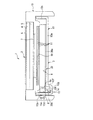
ここで、図8を用いて、従来の照明装置での問題点について具体的に説明する。 Here, the problem in the conventional illumination device will be specifically described with reference to FIG.
図8は、従来の照明装置での問題点を説明する図である。 FIG. 8 is a diagram for explaining a problem in the conventional lighting device.
図8において、従来の液晶表示装置50は、液晶パネル51と、この液晶パネル51の非表示面側に設けられて、当該液晶パネル51に照明光を出射する従来の照明装置52を備えている。従来の照明装置52は、図8の紙面に垂直な方向に沿って、直線状に並べられた複数の発光ダイオード53と、発光ダイオード53の光が入光されるとともに、その光を液晶パネル51側に発光する導光板54と、この導光板54の液晶パネル51とは反対側及び液晶パネル51側にそれぞれ設けられた反射シート55及び光学シート56を具備している。
In FIG. 8, a conventional liquid
また、従来の照明装置52には、フレーム57が設けられており、当該照明装置52の各部が収容されるようになっている。すなわち、フレーム57では、反射シート55、導光板54、及び光学シート56が互いに対向する側面57b、57cの間で底面57a上に設置されている。また、側面57bには、複数の発光ダイオード53が実装された実装基板58が両面テープ59を介して取り付けられている。また、フレーム57では、底面57aと側面57bとの間に溝部57dが設けられており、この溝部57dの内部に実装基板58の端部が配置されている。さらに、フレーム57は、液晶パネル51が取り付けられたプラスチックシャーシ58に一体的に組み付けられるようになっている。
In addition, the
上記のように構成された従来の照明装置52では、底面57aと側面57bとの間に溝部57dが設けられていたので、発光ダイオード53と導光板54との組付精度が低下することがあった。すなわち、従来の照明装置52では、溝部57dを設けたことにより、発光ダイオード53と導光板54との間で、互いに対向する対向方向(図8の左右方向)での距離が大きくなり、これらの発光ダイオード53と導光板54との組付精度の低下を招くことがあった。
In the
具体的にいえば、従来の照明装置52では、発光ダイオード53の発光面(図8の右端の面)が導光板54の入光面(図8の左端の面)に対して、所定位置よりも図8の上下方向で位置ずれした状態で、発光ダイオード53と導光板54とが組み付けられることがあった。このように、組付精度が低下した状態で、発光ダイオード53及び導光板54がフレーム57内に配置されると、図8に3本の矢印にて例示するように、反射シート55によって不必要に反射される光量が部分的に増加し、液晶パネル51側に向かって出射される照明光に輝度ムラが発生して、発光品位が低下した。
Specifically, in the
また、図8に示すように、反射シート55の端部55aが、溝部57dの内部で、図8の下方側に垂れ下がると、発光ダイオード53と導光板54との組付精度によっては発光ダイオード53の光が導光板54に適切に入光されずに、当該光は端部55aにて不適切な方向に反射され易くなり、上記照明光に輝度ムラが生じ易くなって、発光品位の低下も発生し易くなった。
Further, as shown in FIG. 8, when the
なお、上記の説明以外に、反射シート55を設ける代わりに、導光板の下面を反射面として用いたり、フレームの底面を反射面としたりする場合でも、従来の照明装置では、発光ダイオードと導光板との組付精度が悪いと、これらの反射面によって不必要に反射される光量が部分的に増加し、反射シート55を設けた場合と同様に、照明光に輝度ムラが発生して、発光品位が低下した。
In addition to the above description, in the case of using the lower surface of the light guide plate as a reflection surface or the bottom surface of the frame as the reflection surface instead of providing the
上記の課題を鑑み、本発明は、発光ダイオードの設置数を増加したときでも、発光ダイオードと導光板との位置合わせを高精度に行うことができる発光品位に優れた照明装置、及びこれを用いた表示装置を提供することを目的とする。 In view of the above problems, the present invention provides an illumination device excellent in light emission quality and capable of performing alignment between the light emitting diode and the light guide plate with high accuracy even when the number of light emitting diodes is increased, and a lighting device using the same. It is an object to provide a display device.
上記の目的を達成するために、本発明にかかる照明装置は、発光ダイオードと、
複数の前記発光ダイオードが直線状に設けられた実装基板と、
前記発光ダイオードの光が入光される入光面、及び前記入光面から入光された光を発光する発光面を有し、前記入光面から入光された光を所定の伝搬方向に導きつつ、前記発光面から光を出射する導光板と、
前記実装基板が取り付けられる側面、及び前記導光板が載置される底面を有するフレームを備え、
前記フレームには、前記側面と前記底面との間で当該底面よりも前記導光板とは反対側に形成されるとともに、前記実装基板の端部が配置される溝部が設けられ、
前記溝部には、前記導光板を支持する支持部が設置されていることを特徴とするものである。To achieve the above object, a lighting device according to the present invention includes a light emitting diode,
A mounting substrate in which a plurality of the light emitting diodes are linearly provided;
A light incident surface on which light from the light emitting diode is incident; and a light emitting surface that emits light incident from the light incident surface. The light incident from the light incident surface is directed in a predetermined propagation direction. A light guide plate that emits light from the light emitting surface while guiding,
A frame having a side surface to which the mounting substrate is attached and a bottom surface on which the light guide plate is placed;
The frame is provided between the side surface and the bottom surface on the opposite side of the light guide plate from the bottom surface, and is provided with a groove in which an end portion of the mounting substrate is disposed.
The groove portion is provided with a support portion for supporting the light guide plate.
上記のように構成された照明装置では、実装基板の端部が配置される溝部が設けられているので、実装基板に設けられる発光ダイオードの設置数を増加したときでも、当該実装基板をフレームに容易に取り付けることができる。また、溝部には、導光板を支持する支持部が設置されている。これにより、上記従来例と異なり、発光ダイオードの設置数を増加したときでも、発光ダイオードと導光板との位置合わせを高精度に行うことができる。この結果、外部に出射される照明光に輝度ムラが生じるのを防ぐことが可能となり、優れた発光品位を有する照明装置を構成することができる。 In the lighting device configured as described above, since the groove portion in which the end portion of the mounting substrate is disposed is provided, even when the number of light emitting diodes provided on the mounting substrate is increased, the mounting substrate is used as a frame. Easy to install. Moreover, the support part which supports a light-guide plate is installed in the groove part. Thereby, unlike the conventional example, even when the number of light emitting diodes is increased, the alignment between the light emitting diodes and the light guide plate can be performed with high accuracy. As a result, it is possible to prevent uneven brightness from occurring in the illumination light emitted to the outside, and an illumination device having excellent light emission quality can be configured.
また、上記照明装置において、前記実装基板には、前記複数の発光ダイオードが前記導光板の入光面に対向するように直線状に実装された実装部、及び前記溝部の内部に配置されるように前記実装部の前記端部側に設置され、所定の配線パターンが形成された配線部が設けられていることが好ましい。 In the illumination device, the plurality of light emitting diodes may be arranged on the mounting substrate in a linearly mounted manner so as to face the light incident surface of the light guide plate, and inside the groove portion. Preferably, a wiring portion is provided on the end portion side of the mounting portion, and a predetermined wiring pattern is formed.
この場合、発光ダイオードの設置数を増加したときでも、導光板に対して、確実に発光ダイオードを高精度に配置することができる。 In this case, even when the number of light emitting diodes is increased, the light emitting diodes can be reliably arranged with high accuracy with respect to the light guide plate.
また、上記照明装置において、前記導光板と前記底面との間には、前記入光面から入光された光を前記発光面側に反射する反射シートが設けられていることが好ましい。 In the illumination device, it is preferable that a reflection sheet is provided between the light guide plate and the bottom surface to reflect light incident from the light incident surface toward the light emitting surface.
この場合、発光ダイオードの光利用効率を確実に向上することができる。 In this case, the light utilization efficiency of the light emitting diode can be improved with certainty.
また、上記照明装置において、前記支持部として、弾力性を有する支持部材が用いられてもよい。 In the lighting device, a support member having elasticity may be used as the support portion.
この場合、支持部材が弾力性を有しているので、発光ダイオードと導光板との高精度な位置合わせを容易に行うことができる。 In this case, since the support member has elasticity, the light emitting diode and the light guide plate can be easily aligned with high accuracy.
また、上記照明装置において、前記支持部として、前記導光板に対して、弾力性が付与された状態で、支持可能となるように、前記反射シートの端部を所定の形状に折り曲げた折り曲げ部が用いられてもよい。 Further, in the lighting device, as the support portion, a bent portion in which an end portion of the reflection sheet is bent into a predetermined shape so as to be supported in a state where elasticity is applied to the light guide plate. May be used.
この場合、反射シートの折り曲げ部は弾力性が付与された状態で導光板を支持するので、発光ダイオードと導光板との高精度な位置合わせを容易に行うことができる。 In this case, since the bent portion of the reflection sheet supports the light guide plate in a state where elasticity is imparted, the highly accurate alignment between the light emitting diode and the light guide plate can be easily performed.
また、上記照明装置において、前記支持部は、熱伝導性を有していることが好ましい。 Moreover, the said illuminating device WHEREIN: It is preferable that the said support part has thermal conductivity.
この場合、発光ダイオードで生じた熱の放熱性を向上することができる。 In this case, the heat dissipation of the heat generated in the light emitting diode can be improved.
また、本発明の表示装置は、上記いずれかに記載の照明装置を用いたことを特徴とする。 In addition, a display device according to the present invention uses any one of the lighting devices described above.
上記のように構成された表示装置では、発光ダイオードの設置数を増加したときでも、発光ダイオードと導光板との位置合わせを高精度に行うことができる発光品位に優れた照明装置が用いられているので、大型化(大画面化)を図ったときでも、高輝度で、表示品位に優れた表示装置を容易に構成することができる。 In the display device configured as described above, an illuminating device excellent in light emission quality that can perform alignment of the light emitting diode and the light guide plate with high accuracy even when the number of light emitting diodes is increased is used. Therefore, a display device with high luminance and excellent display quality can be easily configured even when the size is increased (the screen is enlarged).
本発明によれば、発光ダイオードの設置数を増加したときでも、発光ダイオードと導光板との位置合わせを高精度に行うことができる発光品位に優れた照明装置、及びこれを用いた表示装置を提供することが可能となる。 According to the present invention, even when the number of installed light emitting diodes is increased, an illumination device excellent in light emitting quality capable of highly accurately aligning the light emitting diodes and the light guide plate, and a display device using the same. It becomes possible to provide.
以下、本発明の照明装置、及びこれを用いた液晶表示装置の好ましい実施形態について、図面を参照しながら説明する。なお、以下の説明では、本発明を透過型の液晶表示装置に適用した場合を例示して説明する。また、各図中の構成部材の寸法は、実際の構成部材の寸法及び各構成部材の寸法比率等を忠実に表したものではない。 Hereinafter, preferred embodiments of a lighting device of the present invention and a liquid crystal display device using the same will be described with reference to the drawings. In the following description, the case where the present invention is applied to a transmissive liquid crystal display device will be described as an example. Moreover, the dimension of the structural member in each figure does not faithfully represent the actual dimension of the structural member, the dimensional ratio of each structural member, or the like.
[第1の実施形態]
図1は、本発明の第1の実施形態にかかる照明装置及び液晶表示装置を説明する図である。図2は、図1に示したフレームの構成を示す斜視図である。図3は、図1に示した実装基板の具体的な構成を示す平面図である。図4は、図1に示した支持部材の具体的な構成を示す斜視図である。[First Embodiment]
FIG. 1 is a diagram for explaining an illumination device and a liquid crystal display device according to a first embodiment of the present invention. FIG. 2 is a perspective view showing the configuration of the frame shown in FIG. FIG. 3 is a plan view showing a specific configuration of the mounting board shown in FIG. FIG. 4 is a perspective view showing a specific configuration of the support member shown in FIG.
図1において、本実施形態の液晶表示装置1では、情報を表示する表示部としての液晶パネル2と、液晶パネル2に照明光を照射する照明装置3とが設けられており、これらの液晶パネル2と照明装置3とが透過型の液晶表示装置1として一体化されている。
In FIG. 1, the liquid crystal display device 1 of the present embodiment is provided with a
液晶パネル2は、一対の基板を構成するCF(Color Filter)基板4及びアクティブマトリクス基板5と、CF基板4及びアクティブマトリクス基板5の各外側表面にそれぞれ設けられた偏光板6、7とを備えている。CF基板4とアクティブマトリクス基板5との間には、図示を省略した液晶層が狭持されている。また、CF基板4及びアクティブマトリクス基板5には、平板状の透明なガラス材またはアクリル樹脂などの透明な合成樹脂が使用されている。偏光板6、7には、TAC(トリアセチルセルロース)またはPVA(ポリビニルアルコール)などの樹脂フィルムが使用されており、液晶パネル2に設けられた表示面の有効表示領域を少なくとも覆うように対応するCF基板4またはアクティブマトリクス基板5に貼り合わせられている。
The
また、アクティブマトリクス基板5は、上記一対の基板の一方の基板を構成するものであり、アクティブマトリクス基板5では、液晶パネル2の表示面に含まれる複数の画素に応じて、画素電極やTFT(Thin Film Transistor)などが上記液晶層との間に形成されている(図示せず)。また、このアクティブマトリクス基板5には、液晶パネル2の駆動制御を行う制御装置(図示せず)に接続されており、上記液晶層を画素単位に動作することで表示面を画素単位に駆動して、当該表示面上に所望画像を表示するようになっている。一方、CF基板4は、一対の基板の他方の基板を構成するものであり、CF基板4には、カラーフィルタや対向電極などが上記液晶層との間に形成されている(図示せず)。
The
尚、液晶パネル2の液晶モードや画素構造は任意である。また、液晶パネル2の駆動モードも任意である。すなわち、液晶パネル2としては、情報を表示できる任意の液晶パネルを用いることができる。それ故、図1においては液晶パネル2の詳細な構造を図示せず、その説明も省略する。
Note that the liquid crystal mode and the pixel structure of the
照明装置3は、図1の紙面に垂直な方向に沿って、直線状に並べられた複数の発光ダイオード8と、発光ダイオード8の光が入光されるとともに、その光を液晶パネル2側に発光する導光板9と、この導光板9の液晶パネル2とは反対側及び液晶パネル2側にそれぞれ設けられた反射シート10及び光学シート11を具備している。この光学シート11には、レンズシートや拡散シートなどの所定の光学シートが含まれている。
The illuminating device 3 receives a plurality of
また、照明装置3には、例えば金属を使用したフレーム12が設けられており、当該照明装置3の各部が収容されるようになっている。すなわち、フレーム12では、反射シート10、導光板9、及び光学シート11が互いに対向する側面12b、12cの間で底面12a上に設置されている。また、側面12bには、例えば熱伝導性を有する両面テープ15を介して、発光ダイオード8を実装した実装基板14が取り付けられている。この実装基板14では、後に詳述するように、複数の発光ダイオード8が直線状に配列されているとともに、所定の配線パターンが形成されている。
The lighting device 3 is provided with a
また、フレーム12は、液晶パネル2が取り付けられたプラスチックシャーシ13に一体的に組み付けられるようになっている。具体的にいえば、フレーム12には、側面12bの外側表面に突起部12dが設けられている。この突起部12dは、図1に示すように、プラスチックシャーシ13側に設けられた切欠部13aに係合するようになっている。つまり、液晶表示装置1では、突起部12dと切欠部13aとが係合することによって、フレーム12とプラスチックシャーシ13とは一体化される。また、このようにフレーム12とプラスチックシャーシ13とが一体化されると、液晶パネル2と照明装置3とは所望の組付状態で一体化される。
Further, the
さらに、フレーム12では、底面12aと側面12bとの間に溝部12eが設けられており、この溝部12eの内部に実装基板14の端部が配置されている。具体的にいえば、図2も参照して、フレーム12は、平板状の底面12aと、底面12aの一辺側で当該底面12aに立設するように形成された側面12cと、底面12aの他辺側で側面12cに対向するように形成された側面12bを備えている。また、フレーム12には、側面12bと底面12aとの間で当該底面12aよりも導光板9とは反対側(図1の下側)に形成された溝部12eが設けられている。つまり、フレーム12では、底面12aの他辺に連続するように、かつ、側面12cとは反対側に延設された側面12fと、側面12bと側面12fとの間で、一端部及び他端部がこれら側面12b及び12fにそれぞれ連続的に形成された下面12gが設けられている。そして、フレーム12では、溝部12eは側面12b、12fと下面12gによって囲まれた空間で構成されている。また、溝部12eでは、底面12aと下面12gとの間の寸法は、実装基板14の大きさに基づいて定められており、実装基板14の端部に設けられた後述の配線部を溝部12eの内部に配置可能に構成されている。
Further, in the
また、図3に示すように、実装基板14では、複数、例えば8個の発光ダイオード8が直線状に並べられた状態で、当該実装基板14の表面上に実装されている。すなわち、この実装基板14には、複数の発光ダイオード8が導光板9の入光面9a(図1)に対向するように直線状に実装された実装部14a、及び溝部12eの内部に配置されるように実装部14aの端部側に設置され、複数の配線17を有する所定の配線パターンが形成された配線部14bが設けられている。このように実装部14aと配線部14bとが実装基板14に設けられているので、本実施形態の照明装置3では、発光ダイオード8の設置数を増加したときでも、導光板9に対して、確実に発光ダイオード8を高精度に配置することができる。
As shown in FIG. 3, in the mounting
各発光ダイオード8には、例えば赤色(R)、緑色(G)、及び青色(B)のRGBの発光ダイオードを一体化した3in1タイプのもの、もしくは青色ダイオードと黄色の蛍光体を用いたものが用いられている。また、各発光ダイオード8には、トップビュータイプのものが用いられており、各発光ダイオード8では、その発光面は図3に図示されている矩形状の平面であり、当該発光面は導光板9の入光面9aに対向配置されている。また、本実施形態の照明装置3では、図3に例示したように、配線17によって4個ずつ直列に接続された発光ダイオード8を1組の発光ダイオード群として、2組の発光ダイオード群が並列に接続されている。また、配線17には、フレキシブル回路基板18に設けられた配線(図示せず)が電気的に接続されており、図示しない電源から発光ダイオード8に電力を供給するようになっている。
Each light-emitting
図1に戻って、導光板9は、発光ダイオード8の上記発光面に対向して、発光ダイオード8の光が入光される入光面9aと、入光面9aから入光された発光ダイオード8の光を発光する発光面9bを有しており、入光面9aから入光された発光ダイオード8の光を所定の伝搬方向(図1の右方向)に導きつつ、発光面9bから光を液晶パネル2側に出射するようになっている。また、導光板9では、フレーム12の底面12aとの間に設けられた反射シート10によって、入光面9aから入光された光が当該導光板9の内部で発光面9b側に反射されるようになっている。
Returning to FIG. 1, the
さらに、導光板9では、図1に示すように、その端部が溝部12e側に突出した状態で、フレーム12の底面12a上に配置されている。また、反射シート10は、その端部が溝部12e側に延設されている。そして、本実施形態の照明装置3では、導光板9が溝部12eに設置された支持部としての支持部材16によって支持されるように構成されている。
Furthermore, as shown in FIG. 1, the
具体的には、図4に示すように、支持部材16は、上面16a、側面16b、及び下面16cを有する角柱状の部材によって構成されている。そして、この支持部材16では、側面16b及び下面16cがそれぞれフレーム12の側面12f及び下面12gに当接した状態で、溝部12e内に設置されており、その上面16aが導光板9の端部の下方で反射シート10に当接することによって当該導光板9を支持するようになっている。
Specifically, as shown in FIG. 4, the
また、支持部材16には、弾力性を有する材料、例えばゴムや発泡材などの材料が用いられており、導光板9に対して、弾力性が付与された状態で、溝部12e内で当該導光板9を支持するようになっている。そして、本実施形態の照明装置3では、導光板9及び反射シート10が底面12a上に載置されたときに、支持部材16の高さ寸法(図1の上下方向の寸法)が調整されることにより、発光ダイオード8の上記発光面と導光板9の入光面9aとが所望位置で互いに対向配置されて、発光ダイオード8と導光板9とが高精度に組み付けられる。
Further, the
以上のように構成された本実施形態の照明装置3では、フレーム12において、実装基板14の端部が配置される溝部12eが設けられているので、実装基板14に設けられる発光ダイオード8の設置数を増加したときでも、当該実装基板14をフレーム12に容易に取り付けることができる。また、本実施形態の照明装置3では、溝部12eには、導光板9を支持する支持部材(支持部)16が設置されている。これにより、本実施形態の照明装置3では、上記従来例と異なり、発光ダイオード8の設置数を増加したときでも、発光ダイオード8と導光板9との位置合わせを高精度に行うことができる。この結果、本実施形態では、外部に出射される照明光に輝度ムラが生じるのを防ぐことが可能となり、優れた発光品位を有する照明装置3を構成することができる。
In the illuminating device 3 of the present embodiment configured as described above, the
また、本実施形態の照明装置3では、図1に示したように、支持部材16が溝部12e側に延設された反射シート10に当接しているので、図8に示した従来例と異なり、反射シート10の端部が溝部12eの内部で図1の下方側に垂れ下がるのを防ぐことができる。これにより、本実施形態の照明装置3では、上記従来例と異なり、発光ダイオード8の光が反射シート10の端部にて不適切な方向に反射されるのを防いで、上記照明光での輝度ムラの発生及び発光品位の低下を防止することができる。
Moreover, in the illuminating device 3 of this embodiment, as shown in FIG. 1, since the
また、本実施形態の照明装置3では、支持部材16に弾力性を有する材料が用いられているので、発光ダイオード8と導光板9との高精度な位置合わせを容易に行うことができる。また、発光ダイオード8に反射シート10が当接したときでも、支持部材16が弾性変形することによって、反射シート10との当接による物理的な力が発光ダイオード8に加わって、当該発光ダイオード8に損傷が生じるのを防ぐことができる。
Further, in the illumination device 3 of the present embodiment, since a material having elasticity is used for the
また、本実施形態では、発光ダイオード8の設置数を増加したときでも、発光ダイオード8と導光板9との位置合わせを高精度に行うことができる発光品位に優れた照明装置3が用いられているので、大型化(大画面化)を図ったときでも、高輝度で、表示品位に優れた液晶表示装置(表示装置)1を容易に構成することができる。
Further, in the present embodiment, the illumination device 3 excellent in light emission quality that can perform alignment between the
また、上記の実施形態の説明以外に、例えば支持部材16の上面16aに光反射性を付与することにより、反射シート10の端部を短くし、当該上面16aを導光板9の端部に直接的に当接させて、支持部材16が導光板9を支持する構成でもよい。
In addition to the description of the above embodiment, for example, by imparting light reflectivity to the
[第2の実施形態]
図5は、本発明の第2の実施形態にかかる照明装置及び液晶表示装置を説明する図である。図6は、図5に示した反射シートの具体的な構成を示す側面図である。図において、本実施形態と上記第1の実施形態との主な相違点は、支持部材の代わりに、導光板に対して、弾力性が付与された状態で、支持可能となるように、反射シートの端部を所定の形状に折り曲げた折り曲げ部を用いた点である。なお、上記第1の実施形態と共通する要素については、同じ符号を付して、その重複した説明を省略する。[Second Embodiment]
FIG. 5 is a diagram illustrating an illumination device and a liquid crystal display device according to the second embodiment of the present invention. FIG. 6 is a side view showing a specific configuration of the reflecting sheet shown in FIG. In the figure, the main difference between the present embodiment and the first embodiment is that the reflection is performed so that the light guide plate can be supported in a state where elasticity is provided instead of the support member. This is a point using a bent portion obtained by bending the end portion of the sheet into a predetermined shape. In addition, about the element which is common in the said 1st Embodiment, the same code | symbol is attached | subjected and the duplicate description is abbreviate | omitted.
つまり、図5及び図6に示すように、本実施形態の照明装置3では、反射シート20には、導光板9の底面(発光面9bの対向面)に当接して、導光板9の内部側に光を反射する本体部20aと、溝部12e側の端部を断面コ字状に折り曲げた折り曲げ部20bとが設けられている。この折り曲げ部20bは、溝部12eに設置されて、導光板9を支持する支持部を構成している。
That is, as shown in FIGS. 5 and 6, in the lighting device 3 of the present embodiment, the
また、この反射シート20には、例えばPET(ポリエチレンテレフタレート)樹脂などの弾力性を有する合成樹脂を用いられている。そして、反射シート20では、折り曲げ部20bは溝部12e側に突出した導光板9の端部に当接することにより、導光板9に対して、弾力性が付与された状態で、当該導光板9を支持するようになっている。すなわち、折り曲げ部20bは、図6に示すように、本体部20aに対して、90°の角度にて折り曲げられた部分20b1と、この部分20b1に対して、90°の角度にて折り曲げられた部分20b2を有しており、折り曲げ部20bは、部分20b2がフレーム12の下面12gに接触した状態で、導光板9を支持するようになっている。
The
以上の構成により、本実施形態では、上記第1の実施形態と同様な作用・効果を奏することができる。また、本実施形態では、反射シート20の折り曲げ部20bは弾力性が付与された状態で導光板9を支持するので、発光ダイオード8と導光板9との高精度な位置合わせを容易に行うことができる。また、発光ダイオード8に反射シート20が当接したときでも、折り曲げ部20bが弾性変形することによって、反射シート20との当接による物理的な力が発光ダイオード8に加わって、当該発光ダイオード8に損傷が生じるのを防ぐことができる。
With the above configuration, the present embodiment can achieve the same operations and effects as the first embodiment. Moreover, in this embodiment, since the bending
尚、上記の説明以外に、図7(a)に示す反射シート30または図7(b)に示す反射シート40を用いることができる。
In addition to the above description, the
すなわち、図7(a)に示すように、反射シート30には、導光板9の底面(発光面9bの対向面)に当接して、導光板9の内部側に光を反射する本体部30aと、溝部12e側の端部を断面L字状に折り曲げた折り曲げ部30bとが設けられている。この折り曲げ部30bは、溝部12eに設置されて、導光板9を支持する支持部を構成している。
That is, as shown in FIG. 7A, the
また、この反射シート30には、反射シート20と同様に、例えばPET(ポリエチレンテレフタレート)樹脂などの弾力性を有する合成樹脂を用いられている。そして、反射シート30では、折り曲げ部30bは溝部12e側に突出した導光板9の端部に当接することにより、導光板9に対して、弾力性が付与された状態で、当該導光板9を支持するようになっている。すなわち、折り曲げ部30bは、図7(a)に示すように、本体部30aに対して、90°の角度にて折り曲げられた部分30b1を有しており、折り曲げ部30bは、部分30b2の端部がフレーム12の下面12gに接触した状態で、導光板9を支持するようになっている。
In addition, similar to the
また、図7(b)に示すように、反射シート40には、導光板9の底面(発光面9bの対向面)に当接して、導光板9の内部側に光を反射する本体部40aと、溝部12e側の端部を断面額縁状に折り曲げた折り曲げ部40bとが設けられている。この折り曲げ部40bは、溝部12eに設置されて、導光板9を支持する支持部を構成している。
Further, as shown in FIG. 7B, the
また、この反射シート40には、反射シート20と同様に、例えばPET(ポリエチレンテレフタレート)樹脂などの弾力性を有する合成樹脂を用いられている。そして、反射シート40では、折り曲げ部40bは溝部12e側に突出した導光板9の端部に当接することにより、導光板9に対して、弾力性が付与された状態で、当該導光板9を支持するようになっている。すなわち、折り曲げ部40bは、図7(b)に示すように、本体部40aに対して、90°の角度にて折り曲げられた部分40b1と、この部分40b1に対して、90°の角度にて折り曲げられた部分40b2と、この部分40b1に対して、90°の角度にて折り曲げられた部分40b3を有しており、折り曲げ部40bは、部分40b2及び部分40b3がフレーム12の下面12g及び側面12fにそれぞれ接触した状態で、導光板9を支持するようになっている。
In addition, similar to the
尚、上記の実施形態はすべて例示であって制限的なものではない。本発明の技術的範囲は特許請求の範囲によって規定され、そこに記載された構成と均等の範囲内のすべての変更も本発明の技術的範囲に含まれる。 The above embodiments are all illustrative and not restrictive. The technical scope of the present invention is defined by the claims, and all modifications within the scope equivalent to the configurations described therein are also included in the technical scope of the present invention.
例えば、上記の説明では、本発明を透過型の液晶表示装置に適用した場合について説明したが、本発明の照明装置はこれに限定されるものではなく、発光ダイオードの光を利用して、画像、文字などの情報を表示する非発光型の表示部を備えた各種表示装置に適用することができる。具体的には、半透過型の液晶表示装置、あるいは液晶パネルをライトバルブに用いた投写型表示装置に本発明の照明装置を好適に用いることができる。 For example, in the above description, the case where the present invention is applied to a transmissive liquid crystal display device has been described. However, the lighting device of the present invention is not limited to this, and an image using light of a light emitting diode is used. The present invention can be applied to various display devices including a non-light emitting display unit that displays information such as characters. Specifically, the illumination device of the present invention can be suitably used for a transflective liquid crystal display device or a projection display device using a liquid crystal panel as a light valve.
また、上記の説明では、互いに対向する2つの側面を有するフレームにおいて、一方の側面と底面との間に溝部を設けるとともに、当該一方の側面に発光ダイオードを実装した実装基板を取り付けた構成について説明したが、本発明のフレームは側面と底面との間で当該底面よりも導光板とは反対側に形成されるとともに、実装基板の端部が配置される溝部が設けられたものであればよく、2つの各側面と底面との間に溝部を設けて、各側面に実装基板を取り付けて、導光板の互いに対向する2つの各側面を上記入光面としてもよい。また、底面の周囲を囲むように、4つの側面を有するフレームを用いて、4つの各側面に実装基板を取り付ける構成でもよい。 Further, in the above description, in a frame having two side surfaces facing each other, a configuration is described in which a groove is provided between one side surface and the bottom surface, and a mounting substrate on which a light emitting diode is mounted is attached to the one side surface. However, the frame of the present invention may be any frame as long as it is formed between the side surface and the bottom surface on the opposite side of the light guide plate from the bottom surface and provided with a groove portion in which the end portion of the mounting substrate is disposed. A groove portion may be provided between each of the two side surfaces and the bottom surface, a mounting substrate may be attached to each side surface, and each of the two side surfaces of the light guide plate facing each other may be used as the light incident surface. Moreover, the structure which attaches a mounting board | substrate to each of the four side surfaces using the frame which has four side surfaces so that the circumference | surroundings of the bottom face may be enclosed may be sufficient.
また、上記の説明では、実装基板上において、直列に接続された4個の発光ダイオードを1組の発光ダイオード群として、2組の発光ダイオード群を並列に接続した、合計8個の発光ダイオードを直線状に設けた場合について説明したが、本発明の実装基板は発光ダイオードが直線状に設けられたものであればよく、発光ダイオードの設置数や接続方法は上記のものに何等限定されない。 In the above description, on the mounting substrate, four light emitting diodes connected in series are set as one set of light emitting diode groups, and two sets of light emitting diode groups are connected in parallel. Although the case where the light emitting diodes are provided in a straight line has been described, the mounting substrate of the present invention may be any light emitting diode provided in a straight line, and the number of light emitting diodes installed and the connection method are not limited to those described above.
また、上記の説明では、反射シートを用いた構成について説明したが、本発明の照明装置は溝部に設置された支持部が導光板を支持する構成であれば何等限定されるものではなく、反射シートの代わりに、導光板の下面を反射面として用いたり、フレームの底面を反射面としたりする構成でもよい。 In the above description, the configuration using the reflection sheet has been described. However, the lighting device of the present invention is not limited to any configuration as long as the support portion installed in the groove portion supports the light guide plate. Instead of the sheet, the lower surface of the light guide plate may be used as a reflection surface, or the bottom surface of the frame may be used as a reflection surface.
但し、上記実施形態のように反射シートを用いる場合の方が、発光ダイオードの光利用効率を確実に向上することができる点で好ましい。 However, the case where the reflective sheet is used as in the above embodiment is preferable in that the light use efficiency of the light emitting diode can be improved with certainty.
また、上記の説明では、支持部としての支持部材または反射シートに熱伝導性を有する材料を用いた場合について説明したが、本発明の支持部は溝部に設置されて導光板を支持するものであれば何等限定されない。 In the above description, the case where a heat conductive material is used for the support member or the reflection sheet as the support portion has been described. However, the support portion of the present invention is installed in the groove portion and supports the light guide plate. There is no limitation as long as there is.
但し、上記実施形態のように熱伝導性を有する材料を支持部に用いる場合の方が、発光ダイオードで生じた熱の放熱性を向上することができる点で好ましく、発光ダイオードの周囲温度を容易に低減して、当該発光ダイオードの長寿命化を図れる点でも好ましい。 However, the case where a material having thermal conductivity is used for the support as in the above embodiment is preferable in that it can improve the heat dissipation of the heat generated in the light emitting diode, and the ambient temperature of the light emitting diode can be easily set. This is also preferable in that the lifetime of the light-emitting diode can be increased.
また、上記の説明では、RGBの発光ダイオードを一体化した3in1タイプを用いた場合について説明したが、本発明は白色に混色可能な複数色の光をそれぞれ発光する複数色の発光ダイオードを用いたものであれば何等限定されない。具体的には、RGBWの発光ダイオードを一体化した、いわゆるフォーインワン(4in1)タイプの発光ダイオードを適用したり、黄色の光及び青色の光を発光する2種類の発光ダイオードを使用したり、青色ダイオードと黄色の蛍光体を用いた発光ダイオードを使用したりすることもできる。また、RGBの発光ダイオードが互いに別個に構成された3つの発光ダイオードを用いることもできる。 In the above description, the case where a 3in1 type in which RGB light emitting diodes are integrated is used. However, the present invention uses light emitting diodes of a plurality of colors that emit light of a plurality of colors that can be mixed with white. If it is a thing, it will not be limited at all. Specifically, a so-called four-in-one (4in1) type light emitting diode in which RGBW light emitting diodes are integrated is used, two types of light emitting diodes that emit yellow light and blue light are used, A light emitting diode using a diode and a yellow phosphor can also be used. Also, three light emitting diodes in which RGB light emitting diodes are configured separately from each other can be used.
また、上記の説明以外に、第1〜第2の各実施形態を適宜組み合わせたものでもよい。 In addition to the above description, the first to second embodiments may be appropriately combined.
本発明は、発光ダイオードの設置数を増加したときでも、発光ダイオードと導光板との位置合わせを高精度に行うことができる発光品位に優れた照明装置、及びこれを用いた表示装置に対して有用である。 The present invention relates to an illumination device excellent in light emission quality capable of performing alignment of a light emitting diode and a light guide plate with high accuracy even when the number of light emitting diodes is increased, and a display device using the same. Useful.
1 液晶表示装置
2 液晶パネル
3 照明装置
8 発光ダイオード
9 導光板
9a 入光面
9b 発光面
10、20、30、40 反射シート
20b、30b、40b 折り曲げ部(支持部)
12 フレーム
12a 底面
12b 側面
12e 溝部
14 実装基板
14a 実装部
14b 配線部
16 支持部材(支持部)DESCRIPTION OF SYMBOLS 1 Liquid
12
Claims (7)
複数の前記発光ダイオードが直線状に設けられた実装基板と、
前記発光ダイオードの光が入光される入光面、及び前記入光面から入光された光を発光する発光面を有し、前記入光面から入光された光を所定の伝搬方向に導きつつ、前記発光面から光を出射する導光板と、
前記実装基板が取り付けられる側面、及び前記導光板が載置される底面を有するフレームを備え、
前記フレームには、前記側面と前記底面との間で当該底面よりも前記導光板とは反対側に形成されるとともに、前記実装基板の端部が配置される溝部が設けられ、
前記溝部には、前記導光板を支持する支持部が設置されている、
ことを特徴とする照明装置。 A light emitting diode;
A mounting substrate in which a plurality of the light emitting diodes are linearly provided;
A light incident surface on which light from the light emitting diode is incident; and a light emitting surface that emits light incident from the light incident surface. The light incident from the light incident surface is directed in a predetermined propagation direction. A light guide plate that emits light from the light emitting surface while guiding,
A frame having a side surface to which the mounting substrate is attached and a bottom surface on which the light guide plate is placed;
The frame is provided between the side surface and the bottom surface on the opposite side of the light guide plate from the bottom surface, and is provided with a groove in which an end portion of the mounting substrate is disposed.
The groove is provided with a support for supporting the light guide plate.
A lighting device characterized by that.
Priority Applications (1)
| Application Number | Priority Date | Filing Date | Title |
|---|---|---|---|
| JP2011523579A JP5368562B2 (en) | 2009-07-23 | 2010-04-07 | Lighting device and display device |
Applications Claiming Priority (4)
| Application Number | Priority Date | Filing Date | Title |
|---|---|---|---|
| JP2009171946 | 2009-07-23 | ||
| JP2009171946 | 2009-07-23 | ||
| JP2011523579A JP5368562B2 (en) | 2009-07-23 | 2010-04-07 | Lighting device and display device |
| PCT/JP2010/056320 WO2011010492A1 (en) | 2009-07-23 | 2010-04-07 | Illuminating device and display device |
Publications (2)
| Publication Number | Publication Date |
|---|---|
| JPWO2011010492A1 JPWO2011010492A1 (en) | 2012-12-27 |
| JP5368562B2 true JP5368562B2 (en) | 2013-12-18 |
Family
ID=43498970
Family Applications (1)
| Application Number | Title | Priority Date | Filing Date |
|---|---|---|---|
| JP2011523579A Expired - Fee Related JP5368562B2 (en) | 2009-07-23 | 2010-04-07 | Lighting device and display device |
Country Status (7)
| Country | Link |
|---|---|
| US (1) | US8678634B2 (en) |
| EP (1) | EP2431653A4 (en) |
| JP (1) | JP5368562B2 (en) |
| CN (1) | CN102472450A (en) |
| BR (1) | BR112012001484A2 (en) |
| RU (1) | RU2491472C1 (en) |
| WO (1) | WO2011010492A1 (en) |
Families Citing this family (18)
| Publication number | Priority date | Publication date | Assignee | Title |
|---|---|---|---|---|
| US9116277B2 (en) * | 2011-01-26 | 2015-08-25 | Sharp Kabushiki Kaisha | Lighting device, display device, and television receiver |
| JP5727249B2 (en) * | 2011-02-02 | 2015-06-03 | トピー工業株式会社 | Surface light emitting device, surface illumination device using surface light emitting device, and advertisement display device |
| KR101832310B1 (en) * | 2011-06-20 | 2018-02-26 | 엘지이노텍 주식회사 | Luminescent element module and light system including the same |
| KR101892921B1 (en) * | 2011-09-19 | 2018-08-29 | 엘지이노텍 주식회사 | Light emitting module and backlight unit having the same |
| WO2013069601A1 (en) * | 2011-11-10 | 2013-05-16 | シャープ株式会社 | Display device and television reception device |
| WO2013077243A1 (en) * | 2011-11-22 | 2013-05-30 | シャープ株式会社 | Illumination device, display device and television receiver |
| US9494722B2 (en) * | 2012-07-27 | 2016-11-15 | Shenzhen China Star Optoelectronics Technology Co., Ltd | Backlight module |
| CN102830544B (en) * | 2012-08-28 | 2015-09-30 | 深圳市华星光电技术有限公司 | Liquid crystal indicator and backlight module thereof and frame unit |
| JP6143050B2 (en) * | 2012-10-10 | 2017-06-07 | Nltテクノロジー株式会社 | Surface emitting device |
| KR20140049649A (en) * | 2012-10-18 | 2014-04-28 | 삼성디스플레이 주식회사 | Display device |
| US9110216B2 (en) | 2012-11-07 | 2015-08-18 | Cooper Technologies Company | Edgelit lighting fixture and assembly |
| US9101001B2 (en) * | 2013-03-15 | 2015-08-04 | C-Marine Dynamics, Inc. | Spectrally-controlled backlighting for LCD displays |
| KR102108214B1 (en) | 2013-06-12 | 2020-05-07 | 엘지디스플레이 주식회사 | Light emitting diode assembly and liquid crystal display device having the same |
| JP2015004709A (en) * | 2013-06-19 | 2015-01-08 | 三菱電機株式会社 | Display device |
| KR102171590B1 (en) * | 2014-02-14 | 2020-10-30 | 삼성디스플레이 주식회사 | Backlight unit |
| US10180534B2 (en) * | 2015-12-30 | 2019-01-15 | Lg Display Co., Ltd. | Borderless display device including display module |
| CN109027731A (en) * | 2018-10-29 | 2018-12-18 | 启东盛丽光电科技有限公司 | The lamps and lanterns of replaceable LED lamp source mould group |
| DE102023202916A1 (en) | 2023-03-30 | 2024-10-02 | Robert Bosch Gesellschaft mit beschränkter Haftung | Display unit and method for producing a display unit |
Citations (5)
| Publication number | Priority date | Publication date | Assignee | Title |
|---|---|---|---|---|
| JP2003090993A (en) * | 2001-09-19 | 2003-03-28 | Kawaguchiko Seimitsu Co Ltd | Backlight structure for liquid crystal display device |
| JP2003315792A (en) * | 2002-04-24 | 2003-11-06 | Nec Lcd Technologies Ltd | Liquid crystal display |
| JP2004213943A (en) * | 2002-12-27 | 2004-07-29 | Casio Comput Co Ltd | Planar lighting device |
| JP2005017964A (en) * | 2003-06-30 | 2005-01-20 | Kawaguchiko Seimitsu Co Ltd | Liquid crystal display device with back light |
| JP2008058860A (en) * | 2006-09-04 | 2008-03-13 | Epson Imaging Devices Corp | Liquid crystal device and electronic device |
Family Cites Families (14)
| Publication number | Priority date | Publication date | Assignee | Title |
|---|---|---|---|---|
| JPH11153785A (en) * | 1997-11-20 | 1999-06-08 | Seiko Epson Corp | Liquid crystal device |
| JP2001022470A (en) | 1999-07-06 | 2001-01-26 | Internatl Business Mach Corp <Ibm> | Computer with illuminator for keyboard |
| TW494295B (en) | 1999-07-06 | 2002-07-11 | Ibm | Computer with illuminator for keyboard |
| JP2003279973A (en) | 2002-03-20 | 2003-10-02 | Kawaguchiko Seimitsu Co Ltd | Backlight attaching structure for liquid crystal display device |
| EP2204688B1 (en) * | 2002-09-03 | 2011-10-26 | Sharp Kabushiki Kaisha | Liquid crystal display device having sound output function and the like and an electronic device using the same |
| JP4482473B2 (en) | 2005-03-25 | 2010-06-16 | シャープ株式会社 | Liquid crystal display |
| JP2006330536A (en) * | 2005-05-30 | 2006-12-07 | Sanyo Epson Imaging Devices Corp | Liquid crystal display device |
| CN100454103C (en) * | 2005-06-01 | 2009-01-21 | 友达光电股份有限公司 | Liquid crystal display with light leakage prevention function and backlight module thereof |
| KR100978045B1 (en) * | 2006-03-13 | 2010-08-26 | 삼성전자주식회사 | Liquid crystal panel assembly and liquid crystal display device comprising the same |
| JP4915911B2 (en) * | 2006-10-02 | 2012-04-11 | 株式会社 日立ディスプレイズ | Liquid crystal display |
| US7766502B2 (en) * | 2007-05-07 | 2010-08-03 | Tresco International Ltd. Co. | Self-illuminated structural panel units and systems including the same |
| JP5295523B2 (en) * | 2007-05-30 | 2013-09-18 | 株式会社ジャパンディスプレイ | Liquid crystal display |
| JP2008305713A (en) * | 2007-06-08 | 2008-12-18 | Fujifilm Corp | Surface illumination device |
| KR101291798B1 (en) * | 2008-06-10 | 2013-07-31 | 엘지디스플레이 주식회사 | Liquid Crystal Display Module And Assembling Method Thereof |
-
2010
- 2010-04-07 BR BR112012001484A patent/BR112012001484A2/en not_active IP Right Cessation
- 2010-04-07 US US13/382,987 patent/US8678634B2/en not_active Expired - Fee Related
- 2010-04-07 RU RU2012106607/07A patent/RU2491472C1/en not_active IP Right Cessation
- 2010-04-07 WO PCT/JP2010/056320 patent/WO2011010492A1/en active Application Filing
- 2010-04-07 CN CN2010800322240A patent/CN102472450A/en active Pending
- 2010-04-07 EP EP10802113.0A patent/EP2431653A4/en not_active Withdrawn
- 2010-04-07 JP JP2011523579A patent/JP5368562B2/en not_active Expired - Fee Related
Patent Citations (5)
| Publication number | Priority date | Publication date | Assignee | Title |
|---|---|---|---|---|
| JP2003090993A (en) * | 2001-09-19 | 2003-03-28 | Kawaguchiko Seimitsu Co Ltd | Backlight structure for liquid crystal display device |
| JP2003315792A (en) * | 2002-04-24 | 2003-11-06 | Nec Lcd Technologies Ltd | Liquid crystal display |
| JP2004213943A (en) * | 2002-12-27 | 2004-07-29 | Casio Comput Co Ltd | Planar lighting device |
| JP2005017964A (en) * | 2003-06-30 | 2005-01-20 | Kawaguchiko Seimitsu Co Ltd | Liquid crystal display device with back light |
| JP2008058860A (en) * | 2006-09-04 | 2008-03-13 | Epson Imaging Devices Corp | Liquid crystal device and electronic device |
Also Published As
| Publication number | Publication date |
|---|---|
| EP2431653A4 (en) | 2013-10-30 |
| CN102472450A (en) | 2012-05-23 |
| JPWO2011010492A1 (en) | 2012-12-27 |
| RU2491472C1 (en) | 2013-08-27 |
| WO2011010492A1 (en) | 2011-01-27 |
| US8678634B2 (en) | 2014-03-25 |
| US20120188790A1 (en) | 2012-07-26 |
| EP2431653A1 (en) | 2012-03-21 |
| BR112012001484A2 (en) | 2019-09-24 |
Similar Documents
| Publication | Publication Date | Title |
|---|---|---|
| JP5368562B2 (en) | Lighting device and display device | |
| US7936411B2 (en) | Light guide plate, backlight assembly including the same, and liquid crystal display device including the same | |
| JP5024793B2 (en) | Display device | |
| US8411229B2 (en) | Backlight unit and liquid crystal display device having the same for improving image quality | |
| US8704964B2 (en) | Liquid crystal display device | |
| US20070070625A1 (en) | Backlight assembly and liquid crystal display module using the same | |
| JP2008305576A (en) | Lighting unit, and liquid crystal display device with the same | |
| JP2010056061A (en) | Backlight unit, and liquid crystal display device using the same | |
| US8421946B2 (en) | Backlight unit and liquid crystal display device having the same | |
| US20150241020A1 (en) | Optical Member and Display Device Having the Same | |
| US20120075883A1 (en) | Edge-type led backlight moudle | |
| KR20090114696A (en) | Backlight unit | |
| WO2011052259A1 (en) | Lighting device, and display device | |
| WO2012026163A1 (en) | Lighting apparatus, display apparatus, and television receiver apparatus | |
| US20110141158A1 (en) | Back light unit and method for assembling the same | |
| KR101321230B1 (en) | Liquid crystal display device | |
| KR102047223B1 (en) | Backlight unit using LED and liquid crystal display device including the same | |
| US20150103258A1 (en) | Lighting device, display device and television device | |
| WO2011083600A1 (en) | Illumination device, and display device | |
| KR20200012478A (en) | Display apparatus | |
| KR20190079145A (en) | Liquid crystal display device the same | |
| JP2019192574A (en) | Composite light guide member, lighting device, and display device | |
| US8823882B2 (en) | Backlight device, display device, and television receiver | |
| KR20090055410A (en) | LCD Display | |
| KR102582503B1 (en) | Liquid crystal display device |
Legal Events
| Date | Code | Title | Description |
|---|---|---|---|
| A131 | Notification of reasons for refusal |
Free format text: JAPANESE INTERMEDIATE CODE: A131 Effective date: 20121220 |
|
| A521 | Request for written amendment filed |
Free format text: JAPANESE INTERMEDIATE CODE: A523 Effective date: 20130214 |
|
| TRDD | Decision of grant or rejection written | ||
| A01 | Written decision to grant a patent or to grant a registration (utility model) |
Free format text: JAPANESE INTERMEDIATE CODE: A01 Effective date: 20130820 |
|
| A61 | First payment of annual fees (during grant procedure) |
Free format text: JAPANESE INTERMEDIATE CODE: A61 Effective date: 20130912 |
|
| R150 | Certificate of patent or registration of utility model |
Ref document number: 5368562 Country of ref document: JP Free format text: JAPANESE INTERMEDIATE CODE: R150 Free format text: JAPANESE INTERMEDIATE CODE: R150 |
|
| LAPS | Cancellation because of no payment of annual fees |