JP5367459B2 - Semiconductor imaging device - Google Patents
Semiconductor imaging device Download PDFInfo
- Publication number
- JP5367459B2 JP5367459B2 JP2009129262A JP2009129262A JP5367459B2 JP 5367459 B2 JP5367459 B2 JP 5367459B2 JP 2009129262 A JP2009129262 A JP 2009129262A JP 2009129262 A JP2009129262 A JP 2009129262A JP 5367459 B2 JP5367459 B2 JP 5367459B2
- Authority
- JP
- Japan
- Prior art keywords
- region
- pixel region
- wiring
- cap layer
- black reference
- Prior art date
- Legal status (The legal status is an assumption and is not a legal conclusion. Google has not performed a legal analysis and makes no representation as to the accuracy of the status listed.)
- Expired - Fee Related
Links
- 239000004065 semiconductor Substances 0.000 title claims description 21
- 238000003384 imaging method Methods 0.000 title claims description 17
- 239000010949 copper Substances 0.000 claims abstract description 60
- RYGMFSIKBFXOCR-UHFFFAOYSA-N Copper Chemical compound [Cu] RYGMFSIKBFXOCR-UHFFFAOYSA-N 0.000 claims abstract description 12
- 229910052802 copper Inorganic materials 0.000 claims abstract description 12
- 238000006243 chemical reaction Methods 0.000 claims abstract description 5
- 229910052581 Si3N4 Inorganic materials 0.000 claims description 15
- HQVNEWCFYHHQES-UHFFFAOYSA-N silicon nitride Chemical compound N12[Si]34N5[Si]62N3[Si]51N64 HQVNEWCFYHHQES-UHFFFAOYSA-N 0.000 claims description 15
- 239000010410 layer Substances 0.000 description 44
- 239000011229 interlayer Substances 0.000 description 17
- 239000000758 substrate Substances 0.000 description 16
- 238000000034 method Methods 0.000 description 14
- VYPSYNLAJGMNEJ-UHFFFAOYSA-N Silicium dioxide Chemical compound O=[Si]=O VYPSYNLAJGMNEJ-UHFFFAOYSA-N 0.000 description 11
- 229910052814 silicon oxide Inorganic materials 0.000 description 11
- 238000009792 diffusion process Methods 0.000 description 9
- 239000001257 hydrogen Substances 0.000 description 9
- 229910052739 hydrogen Inorganic materials 0.000 description 9
- UFHFLCQGNIYNRP-UHFFFAOYSA-N Hydrogen Chemical compound [H][H] UFHFLCQGNIYNRP-UHFFFAOYSA-N 0.000 description 8
- 238000000206 photolithography Methods 0.000 description 7
- 238000004519 manufacturing process Methods 0.000 description 6
- 238000002161 passivation Methods 0.000 description 6
- XUIMIQQOPSSXEZ-UHFFFAOYSA-N Silicon Chemical compound [Si] XUIMIQQOPSSXEZ-UHFFFAOYSA-N 0.000 description 5
- 230000003287 optical effect Effects 0.000 description 5
- 229910052710 silicon Inorganic materials 0.000 description 5
- 239000010703 silicon Substances 0.000 description 5
- 238000002834 transmittance Methods 0.000 description 5
- XAGFODPZIPBFFR-UHFFFAOYSA-N aluminium Chemical compound [Al] XAGFODPZIPBFFR-UHFFFAOYSA-N 0.000 description 4
- 229910052782 aluminium Inorganic materials 0.000 description 4
- 230000004048 modification Effects 0.000 description 4
- 238000012986 modification Methods 0.000 description 4
- 230000003647 oxidation Effects 0.000 description 4
- 238000007254 oxidation reaction Methods 0.000 description 4
- 238000005245 sintering Methods 0.000 description 3
- 238000005229 chemical vapour deposition Methods 0.000 description 2
- 238000010438 heat treatment Methods 0.000 description 2
- 150000002431 hydrogen Chemical class 0.000 description 2
- 239000012535 impurity Substances 0.000 description 2
- 238000002955 isolation Methods 0.000 description 2
- 229910021420 polycrystalline silicon Inorganic materials 0.000 description 2
- 229920005591 polysilicon Polymers 0.000 description 2
- 238000000137 annealing Methods 0.000 description 1
- 230000000903 blocking effect Effects 0.000 description 1
- 230000009977 dual effect Effects 0.000 description 1
- 239000011159 matrix material Substances 0.000 description 1
- 238000005498 polishing Methods 0.000 description 1
- 239000000126 substance Substances 0.000 description 1
- 230000009466 transformation Effects 0.000 description 1
- WFKWXMTUELFFGS-UHFFFAOYSA-N tungsten Chemical compound [W] WFKWXMTUELFFGS-UHFFFAOYSA-N 0.000 description 1
- 229910052721 tungsten Inorganic materials 0.000 description 1
- 239000010937 tungsten Substances 0.000 description 1
Images


Classifications
-
- H—ELECTRICITY
- H10—SEMICONDUCTOR DEVICES; ELECTRIC SOLID-STATE DEVICES NOT OTHERWISE PROVIDED FOR
- H10F—INORGANIC SEMICONDUCTOR DEVICES SENSITIVE TO INFRARED RADIATION, LIGHT, ELECTROMAGNETIC RADIATION OF SHORTER WAVELENGTH OR CORPUSCULAR RADIATION
- H10F39/00—Integrated devices, or assemblies of multiple devices, comprising at least one element covered by group H10F30/00, e.g. radiation detectors comprising photodiode arrays
- H10F39/80—Constructional details of image sensors
- H10F39/811—Interconnections
-
- H—ELECTRICITY
- H10—SEMICONDUCTOR DEVICES; ELECTRIC SOLID-STATE DEVICES NOT OTHERWISE PROVIDED FOR
- H10F—INORGANIC SEMICONDUCTOR DEVICES SENSITIVE TO INFRARED RADIATION, LIGHT, ELECTROMAGNETIC RADIATION OF SHORTER WAVELENGTH OR CORPUSCULAR RADIATION
- H10F39/00—Integrated devices, or assemblies of multiple devices, comprising at least one element covered by group H10F30/00, e.g. radiation detectors comprising photodiode arrays
- H10F39/011—Manufacture or treatment of image sensors covered by group H10F39/12
- H10F39/026—Wafer-level processing
Landscapes
- Solid State Image Pick-Up Elements (AREA)
Abstract
Description
本発明は、例えばCMOSイメージセンサ等の半導体撮像装置に関する。 The present invention relates to a semiconductor imaging device such as a CMOS image sensor.
半導体撮像装置、特にCMOSイメージセンサは、近年微細化が進み、1.4μmピッチ以降では、配線として銅(Cu)を使用するのが一般的である。Cu配線を用いた撮像装置は、Cuの拡散及び酸化を防止するため、Cu配線上にSi3N4膜により構成されたキャップ層が形成される。このSiNキャップ層は、光の透過率を低下させる。このため、画素領域において、光路上のSiNキャップ層が除去されている。 In recent years, semiconductor imaging devices, particularly CMOS image sensors, have been miniaturized, and after 1.4 μm pitch, it is common to use copper (Cu) as wiring. In an imaging device using Cu wiring, a cap layer composed of a Si 3 N 4 film is formed on the Cu wiring to prevent Cu diffusion and oxidation. This SiN cap layer reduces the light transmittance. For this reason, the SiN cap layer on the optical path is removed in the pixel region.
一方、画素領域の周囲には、画素領域とほぼ同様の構成のダミー画素領域、黒基準信号を生成するための黒基準領域、アナログ信号処理領域、及びデジタル信号処理領域としてのロジック回路領域が配置されている。これらの領域には光が照射されず、画素上にCu配線も存在する。このため、SiNキャップ層は除去していない(例えば特許文献1参照)。 On the other hand, around the pixel area, a dummy pixel area having substantially the same configuration as the pixel area, a black reference area for generating a black reference signal, an analog signal processing area, and a logic circuit area as a digital signal processing area are arranged. Has been. These areas are not irradiated with light, and there are Cu wirings on the pixels. For this reason, the SiN cap layer is not removed (see, for example, Patent Document 1).
ところで、半導体装置の処理工程において、例えばゲート酸化膜に生じた未結合手としてのダングリングボンドを水素により終端させる、所謂シンター処理と呼ばれる熱処理が行なわれる。しかし、上記SiNキャップ層は水素を通過しにくいため、シンター処理において、SiNキャップ層が除去された画素領域と、SiNキャップ層を有するダミー画素領域、黒基準領域やロジック回路領域では水素が基板へ導入される量に差が生じる。すなわち、画素領域に比べてダミー画素領域、黒基準領域及びロジック回路領域への水素導入量が少なく、これらの領域においてダングリングボンドが十分に終端されない箇所が残る。このため、ダミー画素領域、黒基準領域やロジック回路領域においてトランジスタのリーク電流が増大し、特に、暗時において、画素領域とダミー画素領域、黒基準領域、アナログ信号処理領域やロジック回路領域の特性に差が生じるという問題があった。 By the way, in the processing step of the semiconductor device, for example, a so-called sintering process is performed in which dangling bonds as dangling bonds generated in the gate oxide film are terminated with hydrogen. However, since the SiN cap layer does not easily pass hydrogen, in the sintering process, hydrogen is transferred to the substrate in the pixel region from which the SiN cap layer has been removed, the dummy pixel region having the SiN cap layer, the black reference region, and the logic circuit region. There is a difference in the amount introduced. That is, the amount of hydrogen introduced into the dummy pixel region, the black reference region, and the logic circuit region is smaller than that in the pixel region, and there are portions where dangling bonds are not sufficiently terminated in these regions. For this reason, transistor leakage current increases in the dummy pixel region, the black reference region, and the logic circuit region. Especially, in the dark, the characteristics of the pixel region, the dummy pixel region, the black reference region, the analog signal processing region, and the logic circuit region are increased. There is a problem that a difference occurs.
本発明は、画素領域とその他の領域の半導体素子の特性を揃えることが可能な半導体撮像装置を提供しようとするものである。 An object of the present invention is to provide a semiconductor imaging device capable of aligning characteristics of semiconductor elements in a pixel region and other regions.
本発明の半導体撮像装置の態様は、複数の光電変換素子が配置された画素領域と、前記画素領域の周辺に配置されたダミー画素領域、黒基準領域、ロジック回路領域を含む回路領域と、前記画素領域及び前記回路領域に配置された銅配線と、前記銅配線上に配置され、シリコン窒化膜により構成されたキャップ層とを具備し、前記画素領域及び前記回路領域の前記銅配線上以外の前記キャップ層が除去され、前記ダミー画素領域において、前記銅配線の無い領域が垂直方向上の同一位置に無いことを特徴とする。 According to an aspect of the semiconductor imaging device of the present invention , a pixel region in which a plurality of photoelectric conversion elements are disposed, a dummy pixel region disposed around the pixel region, a black reference region, a circuit region including a logic circuit region , A copper wiring disposed in the pixel region and the circuit region; and a cap layer disposed on the copper wiring and configured by a silicon nitride film ; and other than on the copper wiring in the pixel region and the circuit region The cap layer is removed, and in the dummy pixel region, the region without the copper wiring is not at the same position in the vertical direction .
本発明は、画素領域とその他の領域の半導体素子の特性を揃えることが可能な半導体撮像装置を提供する。 The present invention provides a semiconductor imaging device capable of aligning characteristics of semiconductor elements in a pixel region and other regions.
以下、本発明の実施の形態について、図面を参照して説明する。 Hereinafter, embodiments of the present invention will be described with reference to the drawings.
図1は、本実施形態が適用される半導体撮像装置の一例を示している。この半導体撮像装置1において、画素領域(PER)2は、後述する複数の画素が行及び列にマトリクス状に配置されている。これら画素は、例えば光電変換素子としてのフォトダイオードとトランジスタにより構成されている。画素領域2の周囲にはダミー画素領域(DMR)3が配置されている。このダミー画素領域3は、例えば画素領域2と同様の構成とされている。ダミー画素領域3の行及び列に対応して黒基準領域4が配置されている。この黒基準領域4は、例えば遮光されたフォトダイオードとトランジスタにより構成され、黒基準信号を生成する。フォトダイオードとトランジスタは、画素領域2と同様の構成とされている。黒基準領域4及びダミー画素領域3の周囲には、アナログ信号回路及びデジタル信号回路を含むロジック回路領域5が形成されている。
FIG. 1 shows an example of a semiconductor imaging device to which this embodiment is applied. In the semiconductor imaging device 1, the pixel region (PER) 2 includes a plurality of pixels, which will be described later, arranged in rows and columns in a matrix. These pixels are composed of, for example, a photodiode as a photoelectric conversion element and a transistor. A dummy pixel region (DMR) 3 is disposed around the
図2は、図1のII−II線に沿った断面図を示している。 FIG. 2 is a cross-sectional view taken along the line II-II in FIG.
半導体基板としてのシリコン基板11内の素子分離領域12は、基板11の表面領域を画素領域(PER)2とダミー画素領域(DPR)3とを分離している。画素領域2とダミー画素領域3の基板11上には、転送トランジスタTa、Tbを構成するゲート電極13a、13bがゲート絶縁膜を介して形成されている。これらゲート電極13a、13bの一方側面に対応する基板11内に光電変換素子としてのN型フォトダイオード領域14a、14b、P型フォトダイオード領域15a、15bが形成され、ゲート電極13a、13bの他方側面に対応する基板11内に例えばドレイン領域としての拡散層16a、16bが形成されている。
An
基板11の上には、ゲート電極13a、13bを覆う第1層間絶縁膜17及び第2層間絶縁膜19が形成されている。第1層間絶縁膜17内に拡散層16に接続されたコンタクト18a、18bが形成され、第2層間絶縁膜19内に第1Cu(銅)配線20a、20b、20cが形成されている。第1Cu配線20a、20bは、コンタクト18a、18bに接続されている。これら第1Cu配線20a、20b、20c上には、例えばシリコン窒化膜により構成された第1キャップ層21が形成されている。この第1キャップ層21は、銅の拡散を防止するものである。この第1キャップ層21は光の透過率が低いため、画素領域2のN型及びP型フォトダイオード14a、15aの上部に位置する部分は除去されている。さらに、この第1キャップ層21は、後述するアニール処理において、水素の透過を妨げる。このため、ダミー画素領域3、図示せぬ黒基準領域4、及びロジック回路領域5において、第1Cu配線上以外の第1キャップ層21が除去されている。
A first
第1キャップ層21及び第2層間絶縁膜19上に第3層間絶縁膜22が形成されている。この第3層間絶縁膜22及び第1キャップ層19内にコンタクト23a、23bが形成され、第3層間絶縁膜22内に第2Cu配線23cが形成されている。コンタクト23a、23bは、第1Cu配線20a、20bにそれぞれ接続されるとともに、第2Cu配線23cに接続されている。第2Cu配線23cの上には、第2キャップ層24が形成されている。この第2キャップ層24も画素領域2の上方、ダミー画素領域3、黒基準領域4、及びロジック回路領域5の第2Cu配線上以外の領域において除去されている。
A third interlayer
第2キャップ層24、第3層間絶縁膜22上にパッシベーション膜としての例えばシリコン酸化膜25が形成され、このシリコン酸化膜25上にパッシベーション膜としての例えばシリコン窒化膜26が形成される。シリコン窒化膜26、シリコン酸化膜25、第2キャップ層24内に例えばアルミニウムにより構成されたボンディングパッド27aが形成されている。このボンディングパッド27aは、第2Cu配線23cに接続されている。
For example, a
また、画素領域2において、フォトダイオード14a、15aに対応するシリコン窒化膜26上にはカラーフィルタ28が形成され、このカラーフィルタ28上にマイクロレンズ29が形成されている。さらに、ダミー画素領域3、黒基準領域4、ロジック回路領域5に対応するシリコン窒化膜26上には、例えばアルミニウムにより構成された遮光膜27bが形成され、ダミー画素領域3、黒基準領域4、ロジック回路領域5は、遮光膜27bにより遮光されている。
In the
次に、図3乃至図7を参照して上記構成の半導体撮像装置の製造方法について説明する。図3乃至図7において、図2と同一部分には同一符号を付す。 Next, a manufacturing method of the semiconductor imaging device having the above configuration will be described with reference to FIGS. 3 to 7, the same parts as those in FIG. 2 are denoted by the same reference numerals.
図3に示すように、例えばP型のシリコン基板11内に例えばシリコン酸化膜により素子分離領域12が形成される。この後、基板11上にゲート絶縁膜としてのシリコン酸化膜、及びポリシリコン層が形成される。これらポリシリコン層及びシリコン酸化膜がエッチングされ、転送トランジスタTa、Tbのゲート電極13a、13bが形成される。これらゲート電極13a、13b及び図示せぬ例えばレジストパターンをマスクとしてN型不純物、及びP型不純物がイオン注入され、N型フォトダイオード14a、14b、P型フォトダイオード15a、15b、及びN型拡散層16a、16bが形成される。
As shown in FIG. 3, for example, an
この後、図4に示すように、基板11上に例えばシリコン酸化膜が例えば化学気相成長(CVD)により堆積される。このシリコン酸化膜が、化学機械的研磨(CMP)法を用いて平坦化され、第1層間絶縁膜17が形成される。この第1層間絶縁膜17に、フォトリソグラフィー法を用いて拡散層16a、16bを露出する第1コンタクトホールが形成され、この第1コンタクトホール内に例えばタングステンが埋め込まれ、コンタクト18a、18bが形成される。
Thereafter, as shown in FIG. 4, for example, a silicon oxide film is deposited on the
次いで、基板11の全面に例えばシリコン酸化膜により構成された第2層間絶縁膜19が堆積される。この第2層間絶縁膜19に、フォトリソグラフィー法を用いてコンタクト18a、18bを露出する第1配線溝やその他の第1配線溝が形成される。その後、全面にCu膜が堆積され、CMP法を用いてCu膜が平坦化され、第1配線溝内に第1Cu配線20a、20b、20cが形成される。続いて、第1Cu配線20a、20b、20cの酸化及び拡散防止のため、第1Cu配線20a、20b、20c及び第2層間絶縁膜19の全面にシリコン窒化膜が堆積され、キャップ層21が形成される。
Next, a second
次に、図5に示すように、光の透過率低下を防止するため、画素領域2の光路上のキャップ層21が、フォトリソグラフィー法を用いて除去される。この時、ダミー画素領域3の第1Cu配線20b、20c上以外のキャップ層21、及び図示せぬ黒基準領域やロジック回路領域の第1Cu配線上以外のキャップ層が除去される。すなわち、例えばダミー画素領域3、黒基準領域及びロジック回路領域において、第1Cu配線上以外のキャップ層21の殆どが除去される。
Next, as shown in FIG. 5, the
次に、図6に示すように、全面に例えばシリコン酸化膜により構成された第3層間絶縁膜22が堆積され、キャップ層21及び第2層間絶縁膜19が覆われる。この後、フォトリソグラフィー法を用いて、第3層間絶縁膜22、キャップ層21に第1Cu配線20a、20bを露出する第2コンタクトホール及び第2コンタクトホールと連通する第2配線溝が形成される。続いて、第2Cu膜が全面に堆積され、CMP法を用いて第2Cu膜が平坦化される。このデュアルダマシン工程により、第2コンタクト23a、23b及び第2Cu配線23cが形成される。この後、全面に第2Cu配線23cの酸化及び拡散防止のためのシリコン窒化膜が堆積され、キャップ層24が形成される。
Next, as shown in FIG. 6, a third
次に、図7に示すように、光の透過率低下を防止するため、画素領域2の光路上のキャップ層24がフォトリソグラフィー法を用いて除去される。この時、ダミー画素領域3や図示せぬ黒基準領域やロジック回路領域においても、第2Cu配線上以外のキャップ層24が除去される。
Next, as shown in FIG. 7, the
次に、図2に示すように、例えばシリコン酸化膜により構成されたパッシベーション膜25とシリコン窒化膜により構成されたパッシベーション膜26が順次堆積される。その後、基板11は、水素ガス雰囲気内で400℃程度の温度により熱処理としてのシンター処理が行われる。この処理により、シリコン窒化膜中に含まれる水素がシリコン基板中に拡散され、シリコンとゲート酸化膜との界面のダングリングボンドが水素により終端される。
Next, as shown in FIG. 2, a
この後、フォトリソグラフィー法を用いて、パッシベーション膜26、25、キャップ層21がエッチングされ、第2Cu配線23cを露出する開口が形成される。次いで、アルミニウム層が堆積され、フォトリソグラフィー法を用いてアルミニウム層がパターニングされる。この結果、開口内にボンディングパッド27aが形成され、ダミー画素領域3や黒基準領域及びロジック回路領域上に光を遮断するための遮光膜27bが形成される。次いで、画素領域2の光路に対応するパッシベーション膜26上にカラーフィルタ28とマイクロレンズ29が形成され、半導体撮像装置としてのCMOSイメージセンサが完成される。カラーフィルタは、例えばR、G、Gr、Gbにより構成されている。
Thereafter, the
上記実施形態によれば、画素領域2では光路上のシリコン窒化膜により構成されたキャップ層21、24を除去している。さらに、ダミー画素領域3や黒基準領域やロジック回路領域の第1、第2Cu配線20b、20c、23c上以外のキャップ層21、24も除去している。このため、熱処理において、画素領域2と、ダミー画素領域3、黒基準領域及びロジック回路領域とにおいて、水素が基板へ入る量を均一化することができる。したがって、画素領域2、ダミー画素領域3、黒基準領域及びロジック回路領域のダングリングボンドを水素により確実に終端させることができ、トランジスタのリーク電流を抑制することができる。このため、画素領域2と、ダミー画素領域3、黒基準領域及びロジック回路領域とにおいて、暗時の出力特性の差を抑制することが可能である。
According to the above-described embodiment, the cap layers 21 and 24 made of the silicon nitride film on the optical path are removed in the
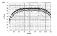
図8、図9は、図1に示すIII−III線(Xアドレス)に沿った画素の暗時の出力レベル(R、G、Gr、Gb)を示すものであり、図8は従来例、図9は本実施形態の場合を示している。 8 and 9 show the output level (R, G, Gr, Gb) of the pixel along the line III-III (X address) shown in FIG. 1 , and FIG. FIG. 9 shows the case of this embodiment.
暗時の出力レベルは、Xアドレスに沿って一定であることが理想である。しかし、図8に示す従来例の場合、ダミー画素領域や黒基準領域及びロジック回路領域において、リーク電流が生じるため、これらの領域からの出力レベルと画素領域からの出力レベルとに約25LSBの差が生じている。 Ideally, the output level in the dark is constant along the X address. However, in the case of the conventional example shown in FIG. 8, since a leak current is generated in the dummy pixel region, the black reference region, and the logic circuit region, the difference between the output level from these regions and the output level from the pixel regions is about 25 LSB. Has occurred.
これに対して、図9に示す本実施形態の場合、ダミー画素領域や黒基準領域及びロジック回路領域のリーク電流が抑制されている。このため、これらの領域からの出力レベルと画素領域からの出力レベルと差は、約5LSBに改善されていることが分かる。 On the other hand, in the present embodiment shown in FIG. 9, the leakage current in the dummy pixel region, the black reference region, and the logic circuit region is suppressed. Therefore, it can be seen that the difference between the output level from these areas and the output level from the pixel area is improved to about 5 LSB.
また、上記実施形態によれば、第1、第2Cu配線20a、20b、20c、及び第1Cu配線23c上にシリコン窒化膜により構成されたキャップ層21、24が形成されている。このため、Cuの拡散及び酸化を防止することが可能である。
Moreover, according to the said embodiment, the cap layers 21 and 24 comprised by the silicon nitride film are formed on the 1st,
図10は、本発明の変形例を示すものである。 FIG. 10 shows a modification of the present invention.
図2に示す実施形態の場合、ダミー画素領域3において、第1Cu配線20bと第1Cu配線20cとの間で第1Cu配線の無い領域と、第2Cu配線23cの無い領域が、垂直方向上のほぼ同一位置に存在している。
In the embodiment shown in FIG. 2, in the
これに対して、図10に示す変形の場合、ダミー画素領域3において、第1Cu配線20bと第1Cu配線20cとの間で第1Cu配線の無い領域と、第2Cu配線23cと第2Cu配線23dとの間で第2Cu配線の無い領域が、垂直方向上の同一位置に無い。しかも、これら第1、第2Cu配線20b、20c、23c、23d上には、光の透過率が低いシリコン窒化膜により構成されたキャップ層21、24が形成されている。したがって、本変形例によれば、遮光性能を向上させることが可能である。
On the other hand, in the case of the modification shown in FIG. 10, in the
また、上記実施形態は、CMOSイメージセンサに本発明を適用した場合について説明したが、これに限らず、Cu配線を用いた他のセンサや半導体装置に適用可能なことは言うまでもない。 Moreover, although the said embodiment demonstrated the case where this invention was applied to a CMOS image sensor, it cannot be overemphasized that it is applicable not only to this but the other sensor and semiconductor device which used Cu wiring.
その他、本発明は、上記実施形態に限定されるものではなく、発明の要旨を変えない範囲において種々変形実施可能なことは勿論である。 In addition, this invention is not limited to the said embodiment, Of course, various deformation | transformation implementation is possible in the range which does not change the summary of invention.
1…半導体撮像装置、2…画素領域、3…ダミー画素領域、4…黒基準領域、5…ロジック回路領域、11…シリコン基板、Ta、Tb…転送トランジスタ、20a、20b、20c…第1Cu配線、23c、23d…第2Cu配線、21、24…キャップ層(シリコン窒化膜)。 DESCRIPTION OF SYMBOLS 1 ... Semiconductor imaging device, 2 ... Pixel area, 3 ... Dummy pixel area, 4 ... Black reference area, 5 ... Logic circuit area, 11 ... Silicon substrate, Ta, Tb ... Transfer transistor, 20a, 20b, 20c ... 1st Cu wiring , 23c, 23d, second Cu wiring, 21, 24, cap layer (silicon nitride film).
Claims (1)
前記画素領域の周辺に配置されたダミー画素領域、黒基準領域、ロジック回路領域を含む回路領域と、
前記画素領域及び前記回路領域に配置された銅配線と、
前記銅配線上に配置され、シリコン窒化膜により構成されたキャップ層と
を具備し、
前記画素領域及び前記回路領域の前記銅配線上以外の前記キャップ層が除去され、前記ダミー画素領域において、前記銅配線の無い領域が垂直方向上の同一位置に無いことを特徴とする半導体撮像装置。 A pixel region in which a plurality of photoelectric conversion elements are disposed;
A circuit region including a dummy pixel region, a black reference region, and a logic circuit region disposed around the pixel region ;
Copper wiring disposed in the pixel region and the circuit region;
A cap layer disposed on the copper wiring and made of a silicon nitride film ,
The semiconductor imaging device, wherein the cap layer other than on the copper wiring in the pixel region and the circuit region is removed, and in the dummy pixel region, the region without the copper wiring is not at the same position in the vertical direction. .
Priority Applications (4)
| Application Number | Priority Date | Filing Date | Title |
|---|---|---|---|
| JP2009129262A JP5367459B2 (en) | 2009-05-28 | 2009-05-28 | Semiconductor imaging device |
| TW099105528A TWI422022B (en) | 2009-05-28 | 2010-02-25 | Semiconductor imaging device and manufacturing method thereof |
| CN2010101330053A CN101901820B (en) | 2009-05-28 | 2010-03-10 | Semiconductor imaging device and its manufacture method |
| US12/725,511 US8816413B2 (en) | 2009-05-28 | 2010-03-17 | Semiconductor imaging device with which semiconductor elements of pixel area and other areas has same characteristics |
Applications Claiming Priority (1)
| Application Number | Priority Date | Filing Date | Title |
|---|---|---|---|
| JP2009129262A JP5367459B2 (en) | 2009-05-28 | 2009-05-28 | Semiconductor imaging device |
Publications (2)
| Publication Number | Publication Date |
|---|---|
| JP2010278232A JP2010278232A (en) | 2010-12-09 |
| JP5367459B2 true JP5367459B2 (en) | 2013-12-11 |
Family
ID=43219273
Family Applications (1)
| Application Number | Title | Priority Date | Filing Date |
|---|---|---|---|
| JP2009129262A Expired - Fee Related JP5367459B2 (en) | 2009-05-28 | 2009-05-28 | Semiconductor imaging device |
Country Status (4)
| Country | Link |
|---|---|
| US (1) | US8816413B2 (en) |
| JP (1) | JP5367459B2 (en) |
| CN (1) | CN101901820B (en) |
| TW (1) | TWI422022B (en) |
Cited By (1)
| Publication number | Priority date | Publication date | Assignee | Title |
|---|---|---|---|---|
| US9553121B2 (en) | 2014-08-28 | 2017-01-24 | Renesas Electronics Corporation | Semiconductor device and method of manufacturing the same |
Families Citing this family (12)
| Publication number | Priority date | Publication date | Assignee | Title |
|---|---|---|---|---|
| JP5513872B2 (en) | 2009-12-18 | 2014-06-04 | 株式会社東芝 | Solid-state imaging device |
| JP5693924B2 (en) | 2010-11-10 | 2015-04-01 | 株式会社東芝 | Semiconductor imaging device |
| JP5826672B2 (en) * | 2012-02-29 | 2015-12-02 | 株式会社東芝 | Image sensor and manufacturing method thereof |
| JP6012987B2 (en) | 2012-02-29 | 2016-10-25 | 株式会社東芝 | Manufacturing method of image sensor |
| FR2990294A1 (en) * | 2012-05-04 | 2013-11-08 | St Microelectronics Crolles 2 | Integrated circuit chip manufacturing method for image forming device, involves performing annealing step in presence of hydrogen between step for covering interconnection level, and step for providing upper aluminum stud above last level |
| FR3009433B1 (en) * | 2013-08-01 | 2015-09-11 | St Microelectronics Crolles 2 | BACKLIGHT ILLUMINATION IMAGE SENSOR WITH LOW DARK CURRENT |
| JP6598436B2 (en) * | 2014-08-08 | 2019-10-30 | キヤノン株式会社 | Photoelectric conversion device, imaging system, and method of manufacturing photoelectric conversion device |
| JP2016146376A (en) | 2015-02-06 | 2016-08-12 | ルネサスエレクトロニクス株式会社 | Imaging apparatus and manufacturing method of the same |
| JP6821291B2 (en) * | 2015-05-29 | 2021-01-27 | キヤノン株式会社 | Manufacturing method of photoelectric conversion device, imaging system and photoelectric conversion device |
| JP6625107B2 (en) * | 2017-10-11 | 2019-12-25 | キヤノン株式会社 | Imaging device |
| EP3931871B1 (en) | 2019-02-28 | 2024-11-06 | Sony Semiconductor Solutions Corporation | Image sensor |
| JP7393471B2 (en) * | 2021-06-03 | 2023-12-06 | シャープ株式会社 | Photoelectric conversion device and X-ray imaging device |
Family Cites Families (11)
| Publication number | Priority date | Publication date | Assignee | Title |
|---|---|---|---|---|
| JP4117672B2 (en) * | 2002-05-01 | 2008-07-16 | ソニー株式会社 | Solid-state imaging device, solid-state imaging device, and manufacturing method thereof |
| US8218052B2 (en) * | 2003-03-07 | 2012-07-10 | Iconix Video, Inc. | High frame rate high definition imaging system and method |
| JP2004311902A (en) | 2003-04-10 | 2004-11-04 | Toshiba Corp | Semiconductor device |
| KR100614793B1 (en) * | 2004-09-23 | 2006-08-22 | 삼성전자주식회사 | Image Sensors and Methods of Manufacturing the Same. |
| KR20070051642A (en) * | 2005-11-15 | 2007-05-18 | 삼성전자주식회사 | Display substrate, manufacturing method thereof and display device having same |
| KR100741099B1 (en) * | 2005-12-20 | 2007-07-20 | 삼성에스디아이 주식회사 | Flat panel display and manufacturing method |
| US20070232074A1 (en) * | 2006-03-31 | 2007-10-04 | Kramadhati Ravi | Techniques for the synthesis of dense, high-quality diamond films using a dual seeding approach |
| US7544982B2 (en) * | 2006-10-03 | 2009-06-09 | Taiwan Semiconductor Manufacturing Company, Ltd. | Image sensor device suitable for use with logic-embedded CIS chips and methods for making the same |
| US7544992B2 (en) * | 2007-05-16 | 2009-06-09 | United Microelectronics Corp. | Illuminating efficiency-increasable and light-erasable embedded memory structure |
| JP4799522B2 (en) * | 2007-10-12 | 2011-10-26 | 株式会社東芝 | Imaging device |
| JP2008199059A (en) | 2008-05-01 | 2008-08-28 | Sony Corp | Solid-state image pickup device and manufacturing method therefor |
-
2009
- 2009-05-28 JP JP2009129262A patent/JP5367459B2/en not_active Expired - Fee Related
-
2010
- 2010-02-25 TW TW099105528A patent/TWI422022B/en not_active IP Right Cessation
- 2010-03-10 CN CN2010101330053A patent/CN101901820B/en not_active Expired - Fee Related
- 2010-03-17 US US12/725,511 patent/US8816413B2/en not_active Expired - Fee Related
Cited By (1)
| Publication number | Priority date | Publication date | Assignee | Title |
|---|---|---|---|---|
| US9553121B2 (en) | 2014-08-28 | 2017-01-24 | Renesas Electronics Corporation | Semiconductor device and method of manufacturing the same |
Also Published As
| Publication number | Publication date |
|---|---|
| TW201106480A (en) | 2011-02-16 |
| US8816413B2 (en) | 2014-08-26 |
| CN101901820B (en) | 2012-11-14 |
| US20100301444A1 (en) | 2010-12-02 |
| JP2010278232A (en) | 2010-12-09 |
| TWI422022B (en) | 2014-01-01 |
| CN101901820A (en) | 2010-12-01 |
Similar Documents
| Publication | Publication Date | Title |
|---|---|---|
| JP5367459B2 (en) | Semiconductor imaging device | |
| JP5693924B2 (en) | Semiconductor imaging device | |
| JP5513872B2 (en) | Solid-state imaging device | |
| JP5357441B2 (en) | Method for manufacturing solid-state imaging device | |
| US20060125007A1 (en) | Local interconnect structure and method for a CMOS image sensor | |
| CN102637712B (en) | Semiconductor device and method for manufacturing the same | |
| JP2008118142A (en) | Image sensor and manufacturing method thereof | |
| JP2016146376A (en) | Imaging apparatus and manufacturing method of the same | |
| US9412778B2 (en) | Semiconductor device, solid-state image sensor, methods of manufacturing the same, and camera | |
| US20170062497A1 (en) | Imaging device and manufacturing method of the same | |
| JP6325904B2 (en) | Solid-state imaging device manufacturing method, solid-state imaging device, and camera | |
| US20160013228A1 (en) | Solid-state imaging device and method for manufacturing solid-state imaging device | |
| US9887220B2 (en) | Method for manufacturing imaging apparatus, and imaging apparatus | |
| JP6630392B2 (en) | Method for manufacturing solid-state imaging device, solid-state imaging device, and camera | |
| JP5950531B2 (en) | Semiconductor device manufacturing method and semiconductor wafer | |
| CN105185801B (en) | Solid-state image pickup device and image pickup system | |
| JP4815769B2 (en) | Solid-state imaging device and manufacturing method thereof | |
| US20240006438A1 (en) | Imaging device | |
| JP2003188368A (en) | Manufacturing method for solid-state imaging device | |
| JP2007194359A (en) | Solid state imaging element, and manufacturing method thereof | |
| JP2006351788A (en) | Solid-state image pickup element and manufacturing method thereof | |
| KR20180006029A (en) | Method for fabricating image sensor |
Legal Events
| Date | Code | Title | Description |
|---|---|---|---|
| A621 | Written request for application examination |
Free format text: JAPANESE INTERMEDIATE CODE: A621 Effective date: 20110802 |
|
| A977 | Report on retrieval |
Free format text: JAPANESE INTERMEDIATE CODE: A971007 Effective date: 20130314 |
|
| A131 | Notification of reasons for refusal |
Free format text: JAPANESE INTERMEDIATE CODE: A131 Effective date: 20130319 |
|
| A521 | Request for written amendment filed |
Free format text: JAPANESE INTERMEDIATE CODE: A523 Effective date: 20130520 |
|
| TRDD | Decision of grant or rejection written | ||
| A01 | Written decision to grant a patent or to grant a registration (utility model) |
Free format text: JAPANESE INTERMEDIATE CODE: A01 Effective date: 20130820 |
|
| A61 | First payment of annual fees (during grant procedure) |
Free format text: JAPANESE INTERMEDIATE CODE: A61 Effective date: 20130911 |
|
| R151 | Written notification of patent or utility model registration |
Ref document number: 5367459 Country of ref document: JP Free format text: JAPANESE INTERMEDIATE CODE: R151 |
|
| LAPS | Cancellation because of no payment of annual fees |