JP5329987B2 - Semiconductor memory device and manufacturing method thereof - Google Patents
Semiconductor memory device and manufacturing method thereof Download PDFInfo
- Publication number
- JP5329987B2 JP5329987B2 JP2009003904A JP2009003904A JP5329987B2 JP 5329987 B2 JP5329987 B2 JP 5329987B2 JP 2009003904 A JP2009003904 A JP 2009003904A JP 2009003904 A JP2009003904 A JP 2009003904A JP 5329987 B2 JP5329987 B2 JP 5329987B2
- Authority
- JP
- Japan
- Prior art keywords
- diode
- film
- variable resistance
- resistance film
- forming
- Prior art date
- Legal status (The legal status is an assumption and is not a legal conclusion. Google has not performed a legal analysis and makes no representation as to the accuracy of the status listed.)
- Active
Links
- 239000004065 semiconductor Substances 0.000 title claims abstract description 62
- 238000004519 manufacturing process Methods 0.000 title claims description 36
- 239000000758 substrate Substances 0.000 claims abstract description 28
- 229910052751 metal Inorganic materials 0.000 claims description 24
- 239000002184 metal Substances 0.000 claims description 24
- 238000000151 deposition Methods 0.000 claims description 8
- 238000005530 etching Methods 0.000 claims description 7
- 239000000463 material Substances 0.000 claims description 5
- XUIMIQQOPSSXEZ-UHFFFAOYSA-N Silicon Chemical compound [Si] XUIMIQQOPSSXEZ-UHFFFAOYSA-N 0.000 abstract description 28
- 229910052710 silicon Inorganic materials 0.000 abstract description 28
- 239000010703 silicon Substances 0.000 abstract description 28
- 239000010410 layer Substances 0.000 description 96
- 238000000034 method Methods 0.000 description 56
- 230000015654 memory Effects 0.000 description 33
- 238000001020 plasma etching Methods 0.000 description 26
- 239000011810 insulating material Substances 0.000 description 12
- 239000011229 interlayer Substances 0.000 description 12
- 239000002019 doping agent Substances 0.000 description 9
- 230000004888 barrier function Effects 0.000 description 8
- 230000000694 effects Effects 0.000 description 8
- PXHVJJICTQNCMI-UHFFFAOYSA-N Nickel Chemical compound [Ni] PXHVJJICTQNCMI-UHFFFAOYSA-N 0.000 description 6
- 230000007547 defect Effects 0.000 description 5
- 230000015572 biosynthetic process Effects 0.000 description 4
- 238000001459 lithography Methods 0.000 description 4
- 239000011572 manganese Substances 0.000 description 4
- 239000011159 matrix material Substances 0.000 description 4
- 229910021420 polycrystalline silicon Inorganic materials 0.000 description 4
- 229920005591 polysilicon Polymers 0.000 description 4
- VYPSYNLAJGMNEJ-UHFFFAOYSA-N Silicium dioxide Chemical compound O=[Si]=O VYPSYNLAJGMNEJ-UHFFFAOYSA-N 0.000 description 3
- 150000001768 cations Chemical class 0.000 description 3
- 229910044991 metal oxide Inorganic materials 0.000 description 3
- 150000004706 metal oxides Chemical class 0.000 description 3
- BASFCYQUMIYNBI-UHFFFAOYSA-N platinum Chemical compound [Pt] BASFCYQUMIYNBI-UHFFFAOYSA-N 0.000 description 3
- 229910052814 silicon oxide Inorganic materials 0.000 description 3
- PWHULOQIROXLJO-UHFFFAOYSA-N Manganese Chemical group [Mn] PWHULOQIROXLJO-UHFFFAOYSA-N 0.000 description 2
- 229910052782 aluminium Inorganic materials 0.000 description 2
- XAGFODPZIPBFFR-UHFFFAOYSA-N aluminium Chemical compound [Al] XAGFODPZIPBFFR-UHFFFAOYSA-N 0.000 description 2
- 230000015556 catabolic process Effects 0.000 description 2
- 238000010586 diagram Methods 0.000 description 2
- 229910052735 hafnium Inorganic materials 0.000 description 2
- VBJZVLUMGGDVMO-UHFFFAOYSA-N hafnium atom Chemical compound [Hf] VBJZVLUMGGDVMO-UHFFFAOYSA-N 0.000 description 2
- 239000012535 impurity Substances 0.000 description 2
- 230000007257 malfunction Effects 0.000 description 2
- 229910052748 manganese Inorganic materials 0.000 description 2
- 229910052759 nickel Inorganic materials 0.000 description 2
- 239000010955 niobium Substances 0.000 description 2
- VSZWPYCFIRKVQL-UHFFFAOYSA-N selanylidenegallium;selenium Chemical compound [Se].[Se]=[Ga].[Se]=[Ga] VSZWPYCFIRKVQL-UHFFFAOYSA-N 0.000 description 2
- 239000000126 substance Substances 0.000 description 2
- 229910052715 tantalum Inorganic materials 0.000 description 2
- GUVRBAGPIYLISA-UHFFFAOYSA-N tantalum atom Chemical compound [Ta] GUVRBAGPIYLISA-UHFFFAOYSA-N 0.000 description 2
- 239000010936 titanium Substances 0.000 description 2
- WFKWXMTUELFFGS-UHFFFAOYSA-N tungsten Chemical compound [W] WFKWXMTUELFFGS-UHFFFAOYSA-N 0.000 description 2
- 229910052721 tungsten Inorganic materials 0.000 description 2
- 239000010937 tungsten Substances 0.000 description 2
- ZOXJGFHDIHLPTG-UHFFFAOYSA-N Boron Chemical compound [B] ZOXJGFHDIHLPTG-UHFFFAOYSA-N 0.000 description 1
- OAICVXFJPJFONN-UHFFFAOYSA-N Phosphorus Chemical compound [P] OAICVXFJPJFONN-UHFFFAOYSA-N 0.000 description 1
- 229910008484 TiSi Inorganic materials 0.000 description 1
- RTAQQCXQSZGOHL-UHFFFAOYSA-N Titanium Chemical compound [Ti] RTAQQCXQSZGOHL-UHFFFAOYSA-N 0.000 description 1
- NRTOMJZYCJJWKI-UHFFFAOYSA-N Titanium nitride Chemical compound [Ti]#N NRTOMJZYCJJWKI-UHFFFAOYSA-N 0.000 description 1
- 229910052785 arsenic Inorganic materials 0.000 description 1
- RQNWIZPPADIBDY-UHFFFAOYSA-N arsenic atom Chemical compound [As] RQNWIZPPADIBDY-UHFFFAOYSA-N 0.000 description 1
- QVGXLLKOCUKJST-UHFFFAOYSA-N atomic oxygen Chemical group [O] QVGXLLKOCUKJST-UHFFFAOYSA-N 0.000 description 1
- 229910052796 boron Inorganic materials 0.000 description 1
- 229910017052 cobalt Inorganic materials 0.000 description 1
- 239000010941 cobalt Substances 0.000 description 1
- GUTLYIVDDKVIGB-UHFFFAOYSA-N cobalt atom Chemical compound [Co] GUTLYIVDDKVIGB-UHFFFAOYSA-N 0.000 description 1
- 239000002131 composite material Substances 0.000 description 1
- 150000001875 compounds Chemical class 0.000 description 1
- 239000004020 conductor Substances 0.000 description 1
- ZXOKVTWPEIAYAB-UHFFFAOYSA-N dioxido(oxo)tungsten Chemical group [O-][W]([O-])=O ZXOKVTWPEIAYAB-UHFFFAOYSA-N 0.000 description 1
- -1 for example Substances 0.000 description 1
- 238000009413 insulation Methods 0.000 description 1
- 230000010354 integration Effects 0.000 description 1
- 229910052741 iridium Inorganic materials 0.000 description 1
- GKOZUEZYRPOHIO-UHFFFAOYSA-N iridium atom Chemical compound [Ir] GKOZUEZYRPOHIO-UHFFFAOYSA-N 0.000 description 1
- YDZQQRWRVYGNER-UHFFFAOYSA-N iron;titanium;trihydrate Chemical group O.O.O.[Ti].[Fe] YDZQQRWRVYGNER-UHFFFAOYSA-N 0.000 description 1
- 229910052758 niobium Inorganic materials 0.000 description 1
- GUCVJGMIXFAOAE-UHFFFAOYSA-N niobium atom Chemical compound [Nb] GUCVJGMIXFAOAE-UHFFFAOYSA-N 0.000 description 1
- 229910052609 olivine Inorganic materials 0.000 description 1
- 239000010450 olivine Substances 0.000 description 1
- 229910052760 oxygen Inorganic materials 0.000 description 1
- 239000001301 oxygen Substances 0.000 description 1
- 230000002093 peripheral effect Effects 0.000 description 1
- 229910052698 phosphorus Inorganic materials 0.000 description 1
- 239000011574 phosphorus Substances 0.000 description 1
- 229910052697 platinum Inorganic materials 0.000 description 1
- 238000005498 polishing Methods 0.000 description 1
- 238000003672 processing method Methods 0.000 description 1
- 238000001004 secondary ion mass spectrometry Methods 0.000 description 1
- 229910052596 spinel Inorganic materials 0.000 description 1
- 239000011029 spinel Substances 0.000 description 1
- MZLGASXMSKOWSE-UHFFFAOYSA-N tantalum nitride Chemical compound [Ta]#N MZLGASXMSKOWSE-UHFFFAOYSA-N 0.000 description 1
- JBQYATWDVHIOAR-UHFFFAOYSA-N tellanylidenegermanium Chemical compound [Te]=[Ge] JBQYATWDVHIOAR-UHFFFAOYSA-N 0.000 description 1
- 229910052719 titanium Inorganic materials 0.000 description 1
- 229910021341 titanium silicide Inorganic materials 0.000 description 1
- 230000007704 transition Effects 0.000 description 1
Images


Classifications
-
- H—ELECTRICITY
- H10—SEMICONDUCTOR DEVICES; ELECTRIC SOLID-STATE DEVICES NOT OTHERWISE PROVIDED FOR
- H10B—ELECTRONIC MEMORY DEVICES
- H10B63/00—Resistance change memory devices, e.g. resistive RAM [ReRAM] devices
- H10B63/80—Arrangements comprising multiple bistable or multi-stable switching components of the same type on a plane parallel to the substrate, e.g. cross-point arrays
-
- H—ELECTRICITY
- H10—SEMICONDUCTOR DEVICES; ELECTRIC SOLID-STATE DEVICES NOT OTHERWISE PROVIDED FOR
- H10B—ELECTRONIC MEMORY DEVICES
- H10B63/00—Resistance change memory devices, e.g. resistive RAM [ReRAM] devices
- H10B63/20—Resistance change memory devices, e.g. resistive RAM [ReRAM] devices comprising selection components having two electrodes, e.g. diodes
-
- H—ELECTRICITY
- H10—SEMICONDUCTOR DEVICES; ELECTRIC SOLID-STATE DEVICES NOT OTHERWISE PROVIDED FOR
- H10D—INORGANIC ELECTRIC SEMICONDUCTOR DEVICES
- H10D84/00—Integrated devices formed in or on semiconductor substrates that comprise only semiconducting layers, e.g. on Si wafers or on GaAs-on-Si wafers
- H10D84/201—Integrated devices formed in or on semiconductor substrates that comprise only semiconducting layers, e.g. on Si wafers or on GaAs-on-Si wafers characterised by the integration of only components covered by H10D1/00 or H10D8/00, e.g. RLC circuits
- H10D84/204—Integrated devices formed in or on semiconductor substrates that comprise only semiconducting layers, e.g. on Si wafers or on GaAs-on-Si wafers characterised by the integration of only components covered by H10D1/00 or H10D8/00, e.g. RLC circuits of combinations of diodes or capacitors or resistors
- H10D84/221—Integrated devices formed in or on semiconductor substrates that comprise only semiconducting layers, e.g. on Si wafers or on GaAs-on-Si wafers characterised by the integration of only components covered by H10D1/00 or H10D8/00, e.g. RLC circuits of combinations of diodes or capacitors or resistors of only diodes
-
- H—ELECTRICITY
- H10—SEMICONDUCTOR DEVICES; ELECTRIC SOLID-STATE DEVICES NOT OTHERWISE PROVIDED FOR
- H10D—INORGANIC ELECTRIC SEMICONDUCTOR DEVICES
- H10D84/00—Integrated devices formed in or on semiconductor substrates that comprise only semiconducting layers, e.g. on Si wafers or on GaAs-on-Si wafers
- H10D84/60—Integrated devices formed in or on semiconductor substrates that comprise only semiconducting layers, e.g. on Si wafers or on GaAs-on-Si wafers characterised by the integration of at least one component covered by groups H10D10/00 or H10D18/00, e.g. integration of BJTs
- H10D84/611—Combinations of BJTs and one or more of diodes, resistors or capacitors
- H10D84/613—Combinations of vertical BJTs and one or more of diodes, resistors or capacitors
- H10D84/617—Combinations of vertical BJTs and only diodes
-
- H—ELECTRICITY
- H10—SEMICONDUCTOR DEVICES; ELECTRIC SOLID-STATE DEVICES NOT OTHERWISE PROVIDED FOR
- H10N—ELECTRIC SOLID-STATE DEVICES NOT OTHERWISE PROVIDED FOR
- H10N70/00—Solid-state devices having no potential barriers, and specially adapted for rectifying, amplifying, oscillating or switching
- H10N70/20—Multistable switching devices, e.g. memristors
-
- H—ELECTRICITY
- H10—SEMICONDUCTOR DEVICES; ELECTRIC SOLID-STATE DEVICES NOT OTHERWISE PROVIDED FOR
- H10N—ELECTRIC SOLID-STATE DEVICES NOT OTHERWISE PROVIDED FOR
- H10N70/00—Solid-state devices having no potential barriers, and specially adapted for rectifying, amplifying, oscillating or switching
- H10N70/801—Constructional details of multistable switching devices
- H10N70/821—Device geometry
- H10N70/826—Device geometry adapted for essentially vertical current flow, e.g. sandwich or pillar type devices
Landscapes
- Semiconductor Memories (AREA)
Abstract
Description
本発明は、半導体記憶装置及びその製造方法に関し、特に、可変抵抗膜を備えた半導体記憶装置及びその製造方法に関する。 The present invention relates to a semiconductor memory device and a manufacturing method thereof, and more particularly to a semiconductor memory device including a variable resistance film and a manufacturing method thereof.
高速且つ大容量な不揮発性メモリを実現するために、フラッシュメモリを始めとして、MRAM(Magneto resistive Random Access Memory:磁気抵抗ランダムアクセスメモリ)及びFeRAM(Feroelectric Random Access Memory:強誘電体RAM)等の様々な不揮発性メモリが開発されている。このような状況の中、昨今、特定の金属酸化物系材料に電圧を印加すると、そのときのセルの状態と電圧によって、その材料が低抵抗状態と高抵抗状態の2つの状態を持つ現象が発見された。このため、この現象を利用した新しい不揮発性メモリ(ReRAM(Resistance Random Access Memory:抵抗変化型メモリ))のアイデアが提案され、注目を集めている。 In order to realize a high-speed and large-capacity nonvolatile memory, various devices such as a flash memory, an MRAM (Magneto resistive Random Access Memory) and a FeRAM (Feroelectric Random Access Memory) are provided. Nonvolatile memories have been developed. Under these circumstances, when a voltage is applied to a specific metal oxide-based material, there is a phenomenon in which the material has two states, a low resistance state and a high resistance state, depending on the cell state and voltage at that time. It's been found. For this reason, an idea of a new nonvolatile memory (ReRAM (Resistance Random Access Memory)) using this phenomenon has been proposed and attracted attention.
ReRAMを実際に製品化する際のデバイス構造としては、メモリセルの集積度を向上させるために、メモリセルを動作させる周辺回路の上に、複数本のワード線が相互に平行に設けられた配線層と、複数本のビット線が相互に平行に設けられた配線層とを交互に積層し、各ワード線と各ビット線との間にメモリセルを接続した3次元型クロスポイント構造が提案されている(例えば、特許文献1参照。)。 A device structure for actually commercializing ReRAM is a wiring in which a plurality of word lines are provided in parallel to each other on a peripheral circuit for operating the memory cells in order to improve the degree of integration of the memory cells. A three-dimensional cross-point structure is proposed in which layers and wiring layers in which a plurality of bit lines are provided in parallel to each other are alternately stacked, and memory cells are connected between each word line and each bit line. (For example, refer to Patent Document 1).
3次元型クロスポイント構造のReRAMにおいては、1本のワード線と1本のビット線を選択することによって、これらの間に接続された1つのメモリセルに選択的に電圧を印加し、そのメモリセルに設けられた可変抵抗素子の抵抗状態を制御して、データを書き込む。そして、各メモリセルに一定の電圧を印加し、流れる電流量を測定することにより、可変抵抗素子の抵抗状態を検出し、書き込まれたデータを読み出す。 In a ReRAM having a three-dimensional cross-point structure, by selecting one word line and one bit line, a voltage is selectively applied to one memory cell connected between them, and the memory Data is written by controlling the resistance state of the variable resistance element provided in the cell. Then, by applying a constant voltage to each memory cell and measuring the amount of flowing current, the resistance state of the variable resistance element is detected, and the written data is read out.
この場合、書込動作においては、例えば、選択した1本のワード線に+5Vの電位を印加し、選択した1本のビット線に0Vの電位を印加することにより、これらの間に接続されたメモリセルに+5Vの電圧を印加する。このとき、選択したワード線と非選択のビット線との間のメモリセル、及び選択したビット線と非選択のワード線との間のメモリセルには電圧が印加されないように、非選択のワード線には選択ビット線と同じ0Vの電位を印加し、非選択のビット線には選択ワード線と同じ+5Vの電位を印加する。しかしながら、そうすると、非選択のワード線と非選択のビット線との間に接続されたメモリセルには、−5Vの電圧が印加されてしまう。 In this case, in the write operation, for example, a potential of +5 V is applied to one selected word line, and a potential of 0 V is applied to one selected bit line, thereby connecting the selected word lines. A voltage of +5 V is applied to the memory cell. At this time, the non-selected word is not applied to the memory cell between the selected word line and the non-selected bit line and the memory cell between the selected bit line and the non-selected word line. The same 0 V potential as that of the selected bit line is applied to the line, and the same +5 V potential as that of the selected word line is applied to the non-selected bit line. However, in this case, a voltage of −5 V is applied to the memory cell connected between the non-selected word line and the non-selected bit line.
そこで、各メモリセルに、ワード線からビット線に向かう方向を順方向とするダイオードを設ける。これにより、選択したメモリセルにおいては、ダイオードに順方向の電圧がかかり、可変抵抗素子に電圧が印加されるが、非選択のワード線と非選択のビット線との間に接続された非選択のメモリセルにおいては、ダイオードに逆方向の電圧が印加されるため、可変抵抗素子には電圧が印加されない。 Therefore, a diode whose forward direction is from the word line to the bit line is provided in each memory cell. As a result, in the selected memory cell, a forward voltage is applied to the diode and a voltage is applied to the variable resistance element, but the non-selection connected between the non-selected word line and the non-selected bit line. In this memory cell, since a reverse voltage is applied to the diode, no voltage is applied to the variable resistance element.
しかしながら、メモリセルにダイオードを設けると、ダイオードの順方向電流が小さいため、可変抵抗素子が高抵抗状態であるときに流れる電流量と低抵抗状態であるときに流れる電流量との差が小さくなり、読出動作のマージンが狭くなってしまうという問題点がある。 However, when a diode is provided in the memory cell, since the forward current of the diode is small, the difference between the amount of current flowing when the variable resistance element is in the high resistance state and the amount of current flowing when the variable resistance element is in the low resistance state is reduced. There is a problem that the margin of the read operation becomes narrow.
本発明の目的は、読出動作のマージンが広い半導体記憶装置及びその製造方法を提供することである。 An object of the present invention is to provide a semiconductor memory device having a wide margin for a read operation and a manufacturing method thereof.
本発明の一態様によれば、基板と、第1の方向に延びる複数本の第1の電位供給線からなる第1の配線層と、前記第1の方向に対して交差する第2の方向に延びる複数本の第2の電位供給線からなる第2の配線層と、前記第1の電位供給線と前記第2の電位供給線との間に配置された可変抵抗膜と、前記可変抵抗膜を挟む前記第1の電位供給線及び前記第2の電位供給線のうち前記基板側に配置された電位供給線と前記可変抵抗膜との間に配置され、前記基板側に配置された電位供給線に沿って延び、前記第1の電位供給線から前記第2の電位供給線に向かう方向に電流を流すダイオードと、前記可変抵抗膜を挟む前記第1の電位供給線及び前記第2の電位供給線のうち前記基板の反対側に配置された電位供給線と前記可変抵抗膜との間に配置された上部電極膜と、を備え、前記第1の配線層及び前記第2の配線層は前記基板上において交互に積層されており、前記ダイオードの上面における前記可変抵抗膜の直下域以外の領域は、前記直下域よりも下方に位置しており、前記ダイオードの太さは前記上部電極膜の太さよりも太いことを特徴とする半導体記憶装置が提供される。 According to one embodiment of the present invention, a substrate, a first wiring layer including a plurality of first potential supply lines extending in the first direction, and a second direction intersecting the first direction A second wiring layer made up of a plurality of second potential supply lines, a variable resistance film disposed between the first potential supply line and the second potential supply line, and the variable resistance Of the first potential supply line and the second potential supply line sandwiching the film, the potential is disposed between the potential supply line disposed on the substrate side and the variable resistance film, and disposed on the substrate side. A diode that extends along a supply line and flows current in a direction from the first potential supply line toward the second potential supply line; the first potential supply line and the second potential sandwiching the variable resistance film; Among the potential supply lines, the potential supply line arranged on the opposite side of the substrate is arranged between the variable resistance film. Comprising an upper electrode films, wherein the first wiring layer and the second wiring layer are alternately stacked on the substrate, a region other than the region directly under the variable resistive film on the upper surface of the diode Is located below the region directly below, and the thickness of the diode is larger than the thickness of the upper electrode film .
本発明の他の一態様によれば、基板上に第1の導電膜を形成する工程と、前記第1の導電膜上に下方に向けて電流を流す第1のダイオードを形成する工程と、前記第1の導電膜及び前記第1のダイオードを第1の方向に沿って分断する工程と、前記第1のダイオード上に第1の可変抵抗膜を形成する工程と、前記第1のダイオードの上部及び前記第1の可変抵抗膜を前記第1の方向及び前記第1の方向に対して交差する第2の方向の双方に沿って分断する工程と、前記第1の可変抵抗膜上に第2の導電膜を形成する工程と、前記第2の導電膜上に上方に向けて電流を流す第2のダイオードを形成する工程と、前記第2の導電膜及び前記第2のダイオードを前記第2の方向に沿って分断する工程と、前記第2のダイオード上に第2の可変抵抗膜を形成する工程と、前記第2のダイオードの上部及び前記第2の可変抵抗膜を前記第1の方向及び前記第2の方向の双方に沿って分断する工程と、を備えたことを特徴とする半導体記憶装置の製造方法が提供される。 According to another aspect of the present invention, a step of forming a first conductive film on a substrate, a step of forming a first diode that causes a current to flow downward on the first conductive film, Separating the first conductive film and the first diode along a first direction, forming a first variable resistance film on the first diode, and Dividing the upper portion and the first variable resistance film along both the first direction and a second direction intersecting the first direction; and a step on the first variable resistance film. Forming a second conductive film; forming a second diode for passing an electric current upward on the second conductive film; and connecting the second conductive film and the second diode to the first conductive film. And a second variable resistance film formed on the second diode. And a step of dividing the upper part of the second diode and the second variable resistance film along both the first direction and the second direction. A method for manufacturing a semiconductor memory device is provided.
本発明の更に他の一態様によれば、基板上に第1の導電膜を形成する工程と、前記第1の導電膜上に下方に向けて電流を流す第1のダイオードを形成する工程と、前記第1のダイオード上に第1の可変抵抗膜を形成する工程と、前記第1の導電膜、前記第1のダイオード及び前記第1の可変抵抗膜を第1の方向に沿って分断する工程と、前記第1の可変抵抗膜上に第2の導電膜を形成する工程と、前記第2の導電膜上に上方に向けて電流を流す第2のダイオードを形成する工程と、前記第2のダイオード上に第2の可変抵抗膜を形成する工程と、前記第1のダイオードの上部、前記第1の可変抵抗膜、前記第2の導電膜、前記第2のダイオード及び前記第2の可変抵抗膜を、前記第1の方向に対して交差する第2の方向に沿って分断する工程と、を備えたことを特徴とする半導体記憶装置の製造方法が提供される。 According to still another aspect of the present invention, a step of forming a first conductive film on a substrate, and a step of forming a first diode that causes a current to flow downward on the first conductive film, Forming a first variable resistance film on the first diode, and dividing the first conductive film, the first diode, and the first variable resistance film along a first direction. Forming a second conductive film on the first variable resistance film; forming a second diode for passing a current upward on the second conductive film; and Forming a second variable resistance film on the two diodes; an upper portion of the first diode; the first variable resistance film; the second conductive film; the second diode; and the second diode. A step of dividing the variable resistance film along a second direction intersecting the first direction; The method of manufacturing a semiconductor memory device characterized by comprising a are provided.
本発明によれば、読出動作のマージンが広い半導体記憶装置及びその製造方法を実現することができる。 According to the present invention, it is possible to realize a semiconductor memory device having a wide margin for a read operation and a manufacturing method thereof.
以下、図面を参照しつつ、本発明の実施形態について説明する。
先ず、本発明の第1の実施形態について説明する。
本実施形態に係る半導体記憶装置は、抵抗変化型メモリ(ReRAM)である。
図1は、本実施形態に係る半導体記憶装置を例示する斜視図であり、
図2は、図1に示す半導体記憶装置の一部を例示する斜視図であり、
図3は、図1に示す半導体記憶装置の一部を例示する断面図であり、
図4は、図3に相当する回路図である。
Hereinafter, embodiments of the present invention will be described with reference to the drawings.
First, a first embodiment of the present invention will be described.
The semiconductor memory device according to the present embodiment is a resistance change memory (ReRAM).
FIG. 1 is a perspective view illustrating a semiconductor memory device according to this embodiment.
FIG. 2 is a perspective view illustrating a part of the semiconductor memory device shown in FIG.
3 is a cross-sectional view illustrating a part of the semiconductor memory device shown in FIG.
FIG. 4 is a circuit diagram corresponding to FIG.
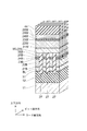
図1に示すように、本実施形態に係る半導体記憶装置1においては、シリコン基板11が設けられており、シリコン基板11の上層部分及び上面上には、半導体記憶装置1の駆動回路(図示せず)が形成されている。シリコン基板11上には、駆動回路を埋め込むように、例えばシリコン酸化物からなる層間絶縁膜12が設けられており、層間絶縁膜12上にはメモリセル部13が設けられている。
As shown in FIG. 1, in the
メモリセル部13においては、シリコン基板11の上面に平行な方向(以下、「ワード線方向」という)に延びる複数本のワード線WLからなるワード線配線層14と、シリコン基板11の上面に平行な方向であって、ワード線方向に対して交差、例えば直交する方向(以下、「ビット線方向」という)に延びる複数本のビット線BLからなるビット線配線層15とが、絶縁層を介して交互に積層されている。ワード線WL及びビット線BLは導電体、例えば、金属により形成されている。また、ワード線WL同士、ビット線BL同士、ワード線WLとビット線BLとは、相互に接していない。そして、各ワード線WLと各ビット線BLとの最近接部分には、シリコン基板11の上面に対して垂直な方向(以下、「上下方向」という)に延びるピラー16が設けられている。
In the
図2及び図3に示すように、各ワード線WLの直上域には下部電極膜21Wが設けられており、その上にはpinダイオード22Wが設けられている。pinダイオード22Wの形状は、その直下のワード線WLに沿ってワード線方向に延びるライン状である。pinダイオード22Wは例えばポリシリコンにより形成されており、下層側から順に、p型層22p、i型層22i、n型層22nがこの順に積層されている。pinダイオード22W上には、中間電極膜23W、可変抵抗膜(ReRAM膜)24W、上部電極膜25W及びストッパ膜26Wがこの順に設けられており、ストッパ膜26Wはその上に配置されたビット線BLに接続されている。すなわち、あるワード線WLとその1段上方に配置されたビット線BLとの間には、下から上に向かって、下部電極膜21W、pinダイオード22W、中間電極膜23W、可変抵抗膜24W、上部電極膜25W及びストッパ膜26Wがこの順に直列に配列されている。
As shown in FIG. 2 and FIG. 3, a
また、各ビット線BLの直上域には下部電極膜21Bが設けられており、その上にはpinダイオード22Bが設けられている。pinダイオード22Bの形状は、その直下のビット線BLに沿ってビット線方向に延びるライン状である。pinダイオード22Bも例えばポリシリコンにより形成されており、下層側から順に、n型層22n、i型層22i、p型層22pがこの順に積層されている。pinダイオード22B上には、中間電極膜23B、可変抵抗膜24B、上部電極膜25B及びストッパ膜26Bがこの順に設けられており、ストッパ膜26Bはその上に配置されたワード線WLに接続されている。すなわち、あるビット線BLとその1段上方に配置されたワード線WLとの間には、下から上に向かって、下部電極膜21B、pinダイオード22B、中間電極膜23B、可変抵抗膜24B、上部電極膜25B及びストッパ膜26Bがこの順に直列に配列されている。
Further, a
これにより、図4に示すように、pinダイオード22W及び22B(以下、総称して、「pinダイオード22」ともいう。他の構成要素についても同様である)は、ワード線WLとビット線BLとの間に、ワード線WLからビット線BLに向かう方向には電流を流すが、ビット線BLからワード線WLに向かう方向には電流を流さないような方向に接続されている。また、pinダイオード22は、同じピラー16に属する可変抵抗膜24よりも下方、すなわち、シリコン基板11側に配置されている。
As a result, as shown in FIG. 4,
なお、下部電極膜21、中間電極膜23、上部電極膜25は金属により形成されており、ストッパ膜26はより硬質な金属、例えばタングステン(W)により形成されている。
また、可変抵抗膜24は、例えば、金属酸化物により形成されており、例えば、少なくとも2種類の陽イオン元素を含む複合化合物により形成されている。陽イオン元素のうち、少なくとも1種類は電子が不完全に満たされたd軌道を持つ遷移元素であり、隣り合う陽イオン元素間の最短距離は0.32nm以下である。具体的には、可変抵抗膜24を形成する元素は、A及びMを相互に異なる元素とするとき、化学式AxMyXzで表される材料であり、例えば、スピネル構造(AM2O4)、イルメナイト構造(AMO3)、デラフォサイト構造(AMO2)、LiMoN2構造(AMN2)、ウルフラマイト構造(AMO4)、オリビン構造(A2MO4)、ホランダイト構造(AxMO2)、ラムスデライト構造(AxMO4)、ペロブスカイト構造(AMO3)等の結晶構造を持つ材料である。一例では、Aは亜鉛(Zn)、Mはマンガン(Mn)、Xは酸素(O)である。又は、可変抵抗膜24は、アルミニウム(Al)、チタン(Ti)、Mn(マンガン)、ニッケル(Ni)、コバルト(Co)、ジルコニウム(Zr)、ニオブ(Nb)、ハフニウム(Hf)、タンタル(Ta)及びタングステン(W)のうち、少なくとも1種の金属を含む絶縁膜である。
The lower electrode film 21, the intermediate electrode film 23, and the upper electrode film 25 are made of metal, and the stopper film 26 is made of a harder metal such as tungsten (W).
The variable resistance film 24 is made of, for example, a metal oxide, and is made of, for example, a composite compound containing at least two kinds of cation elements. At least one of the cation elements is a transition element having a d orbital incompletely filled with electrons, and the shortest distance between adjacent cation elements is 0.32 nm or less. Specifically, the element forming the variable resistance film 24 is a material represented by the chemical formula A x M y X z when A and M are different from each other, for example, a spinel structure (AM 2 O 4 ), ilmenite structure (AMO 3 ), delafossite structure (AMO 2 ), LiMoN 2 structure (AMN 2 ), wolframite structure (AMO 4 ), olivine structure (A 2 MO 4 ), hollandite structure (A x MO 2) ), A ramsdellite structure (A x MO 4 ), a perovskite structure (AMO 3 ), and the like. In one example, A is zinc (Zn), M is manganese (Mn), and X is oxygen (O). Alternatively, the variable resistance film 24 is made of aluminum (Al), titanium (Ti), Mn (manganese), nickel (Ni), cobalt (Co), zirconium (Zr), niobium (Nb), hafnium (Hf), tantalum ( It is an insulating film containing at least one metal of Ta) and tungsten (W).
そして、pinダイオード22の上部と、その上に積層された中間電極膜23、可変抵抗膜24、上部電極膜25及びストッパ膜26は、上下方向に延びる柱状にパターニングされており、ピラー16を構成している。図1〜図3に示す例ではピラー16の形状は四角柱状であるが、本実施形態はこれに限定されず、例えば、後述の図8〜図10に示すように円柱状でもよい。
The upper part of the pin diode 22 and the intermediate electrode film 23, the variable resistance film 24, the upper electrode film 25, and the stopper film 26 stacked on the pin diode 22 are patterned in a column shape extending in the vertical direction, thereby forming the
一方、pinダイオード22Wの下部は、その直下のワード線WLに沿ってワード線方向に延びており、複数本のピラー16の直下域をつなぐように連続的に配設されている。同様に、pinダイオード22Bの下部は、その直下のビット線BLに沿ってビット線方向に延びており、複数本のピラー16の直下域をつなぐように連続的に配設されている。このため、pinダイオード22W及び22Bの上面における可変抵抗膜24の直下域A以外の領域Bは、可変抵抗膜24の直下域Aよりも下方に位置している。
On the other hand, the lower portion of the
pinダイオード22の各層の厚さは例えば35nmよりも厚く、pinダイオード22の全体の厚さは例えば200nmである。そして、領域Bの上下方向の位置は、pinダイオード22を構成する電気的性質が相互に異なる複数の層、すなわち、p型層22p、i型層22i、n型層22nのうち、上から1番目の層と2番目の層との界面以下であり、且つ、この界面から35nm下方の位置以上であることが好ましい。つまり、pinダイオード22Wについては、領域Bの位置は、上から1番目の層であるn型層22nと2番目の層であるi型層22iとの界面の位置と、この界面から35nm下方の位置との間であることが好ましい。この理由は後述する。
The thickness of each layer of the pin diode 22 is thicker than 35 nm, for example, and the entire thickness of the pin diode 22 is 200 nm, for example. The vertical position of the region B is 1 from the top among a plurality of layers having different electrical properties constituting the pin diode 22, that is, the p-
pinダイオードにおけるn型層及びp型層とi型層との相違点は、実効的なドーパントの濃度にある。メモリセル1個当たりのドーパントの数が平均して1個未満であれば、この部分の導電型はi型であるといえる。そこで、pinダイオードにおけるn型層とi型層との界面、又はp型層とi型層との界面を特定するためには、上下方向に沿ってドーパントの濃度プロファイルを取得し、メモリセル1個当たりのドーパント数が平均1個となるようなドーパント濃度をとる位置を特定すればよい。具体的には、例えば、二次イオン質量分析法(SIMS)を用いて面積が数百μm2程度の比較的大きな領域を分析し、pinダイオードの上下方向におけるドーパント濃度のプロファイルを取得する。一辺の長さが数十nm程度のメモリセルの場合、メモリセル1個当たりのドーパント数が平均1個となるようなドーパント濃度は、10×10 17 cm−3程度である。従って、上述のプロファイルにおいてドーパント濃度がこの値となった位置が、n型層又はp型層とi型層との界面である。
The difference between the n-type layer and the p-type layer and the i-type layer in the pin diode is in the effective dopant concentration. If the average number of dopants per memory cell is less than 1, it can be said that the conductivity type of this portion is i-type. Therefore, in order to specify the interface between the n-type layer and the i-type layer or the interface between the p-type layer and the i-type layer in the pin diode, a dopant concentration profile is obtained along the vertical direction, and the
一方、メモリセル部13においては、ワード線WL、ビット線BL、pinダイオード22及びピラー16等は、絶縁材料27によって埋め込まれている。絶縁材料27は、例えば、シリコン酸化物である。
On the other hand, in the
次に、本実施形態の作用効果について説明する。
本実施形態においては、pinダイオード22Wの下部及びpinダイオード22Bの下部がそれぞれワード線方向及びビット線方向に延びているため、上下方向から見て、pinダイオード22W及び22Bの面積が大きい。このため、順方向電流が大きく、可変抵抗膜24が低抵抗状態であるときにワード線WLからビット線BLに流れる電流が大きい。これにより、可変抵抗膜24が低抵抗状態であるときの電流量と高抵抗状態であるときの電流量との差が大きく、読出動作のマージンが広い。この結果、メモリセルの誤動作を防止することができる。
Next, the effect of this embodiment is demonstrated.
In the present embodiment, since the lower part of the
また、後述の第2乃至第4の実施形態において詳細に説明するように、半導体記憶装置1の製造に際して、各ピラー16は、上方からRIE(Reactive Ion Etching:反応性イオンエッチング)等の異方性エッチングを行うことによって形成される。このとき、金属酸化物等からなる可変抵抗膜24はエッチングが困難であるため、可変抵抗膜24の形状は、下面が上面よりも広いテーパー状になり、ピラー16における可変抵抗膜24よりも下方の部分の太さは、可変抵抗膜24よりも上方の部分の太さよりも太くなることが多い。本実施形態においては、pinダイオード22は常に可変抵抗膜24よりも下方に配置されるため、可変抵抗膜24よりも上方に配置する場合と比較して、上下方向から見た面積を大きくすることができる。これにより、順方向電流がより一層増大し、読出動作のマージンが広くなる。
Further, as will be described in detail in the second to fourth embodiments described later, when the
更に、ダイオードをRIE等によって加工すると、加工面、すなわち、ダイオードの側面がプラズマに曝されてダメージを受け、欠陥が導入される。そして、この欠陥に電子がトラップされて固定電荷となり、順方向電流を減少させる。本実施形態においては、pinダイオード22の下部をライン状に形成しているため、ダイオード全体をピラー状に形成する場合と比較して、ダイオードの側面の面積が小さい。従って、ダイオードに導入される欠陥の総量が少なく、固定電荷が少なく、順方向電流が大きい。 Further, when the diode is processed by RIE or the like, the processed surface, that is, the side surface of the diode is exposed to plasma and damaged, and defects are introduced. Then, electrons are trapped in this defect and become a fixed charge, thereby reducing the forward current. In the present embodiment, since the lower portion of the pin diode 22 is formed in a line shape, the area of the side surface of the diode is small as compared with the case where the entire diode is formed in a pillar shape. Therefore, the total amount of defects introduced into the diode is small, the fixed charge is small, and the forward current is large.
更にまた、本実施形態においては、ダイオードをその下端までピラー状に加工する必要がないため、微細化が容易である。また、ピラーの加工に要する時間を短縮することができる。 Furthermore, in the present embodiment, since it is not necessary to process the diode into a pillar shape up to its lower end, miniaturization is easy. Further, the time required for processing the pillar can be shortened.
本実施形態においては、ダイオードの上部はワード線方向及びビット線方向の双方に沿って分断してピラー状に成形し、ダイオードの下部はワード線方向及びビット線方向のうち一方向に沿ってのみ分断してライン状に成形している。ここで、ダイオードをピラー状に加工する際の掘込量によって、ピラー状に成形する上部とライン状に成形する下部との境界の位置、すなわち、ダイオードの上面における領域Bの上下方向の位置が変化するが、この領域Bの位置によって、ダイオードの特性が異なる。 In the present embodiment, the upper part of the diode is divided along both the word line direction and the bit line direction and formed into a pillar shape, and the lower part of the diode is only along one direction of the word line direction and the bit line direction. Divided into a line shape. Here, the position of the boundary between the upper part formed in the pillar shape and the lower part formed in the line shape, that is, the vertical position of the region B on the upper surface of the diode is determined depending on the amount of digging when the diode is processed into the pillar shape. Although it changes, the characteristics of the diode differ depending on the position of the region B.
領域Bの位置が高いほど、上述のダイオードの面積を大きくして順方向電流を増大させる効果及び欠陥を低減させて順方向電流を増大させる効果は大きくなる。また、領域Bがダイオードのpn接合面よりも上方に位置していれば、pn接合面の面積が増えて逆方向電圧が分散される。この結果、ダイオードの逆方向耐圧が高くなり、書込動作及び消去動作のマージンが広くなる。 The higher the position of the region B, the greater the effect of increasing the forward current by increasing the area of the diode and the effect of increasing the forward current by reducing defects. Further, if the region B is located above the pn junction surface of the diode, the area of the pn junction surface increases and the reverse voltage is dispersed. As a result, the reverse breakdown voltage of the diode is increased, and the margin for the write operation and the erase operation is widened.
その反面、領域Bがダイオードのpn接合面よりも上方に位置していると、ダイオードが延びる方向に沿ったリーク電流が増大し、誤動作が生じやすくなる。例えば、pinダイオード22Bの領域Bがpn接合面よりも上方にあると、pinダイオード22Bの最上層であるp型層22pを介してリーク電流が流れやすくなり、このpinダイオード22Bにピラー16を介して接続されたワード線WL同士が短絡しやすくなる。なお、pinダイオード22B上の中間電極膜23が島状に分断されていないと、ワード線WL同士はほぼ確実に短絡する。
On the other hand, if the region B is located above the pn junction surface of the diode, the leakage current along the direction in which the diode extends increases, and malfunction is likely to occur. For example, if the region B of the
逆に、領域Bの位置が低いと、上述の順方向電流を増大させる効果はやや減少し、逆方向耐圧を向上させる効果は得られなくなる。しかし、ワード線WL同士及びビット線BL同士を電気的に確実に分離することができる。 Conversely, when the position of the region B is low, the effect of increasing the forward current described above is slightly reduced, and the effect of improving the reverse breakdown voltage cannot be obtained. However, the word lines WL and the bit lines BL can be electrically isolated from each other.
そこで、本実施形態においては、領域Bの上下方向の位置は、ダイオードを構成する複数の層のうち、上から1番目の層と2番目の層との界面以下であり、且つ、この界面から35nm下方の位置以上とする。すなわち、pinダイオード22Wについては、領域Bの位置はn型層22nとi型層22iとの界面から下方に0乃至35nmの位置とし、pinダイオード22Bについては、領域Bの位置はp型層22pとi型層22iとの界面から下方に0乃至35nmの位置とする。その理由は、ピラーを加工する際の加工ばらつきは目標位置に対して±15nm程度であるところ、領域Bの上下方向の位置を上述の範囲内に位置させれば、領域Bを確実にpn接合面よりも下方に位置させ、ワード線WL間の短絡及びビット線BL間の短絡を確実に防止でき、好ましいからである。
Therefore, in the present embodiment, the vertical position of the region B is equal to or lower than the interface between the first layer and the second layer from the top among the plurality of layers constituting the diode, and from this interface. More than 35 nm below. That is, for the
次に、本発明の第2の実施形態について説明する。
本実施形態は、半導体記憶装置の製造方法の実施形態である。
図5〜図10は、本実施形態に係る半導体記憶装置の製造方法を例示する工程斜視図である。
本実施形態において製造される半導体記憶装置の構成は、前述の第1の実施形態に係る半導体記憶装置の構成とほぼ同じである。
Next, a second embodiment of the present invention will be described.
The present embodiment is an embodiment of a method for manufacturing a semiconductor memory device.
5 to 10 are process perspective views illustrating the method for manufacturing the semiconductor memory device according to this embodiment.
The configuration of the semiconductor memory device manufactured in the present embodiment is substantially the same as the configuration of the semiconductor memory device according to the first embodiment described above.
先ず、図5に示すように、シリコン基板11の上面に駆動回路を形成する。次に、シリコン基板11上に、駆動回路を埋め込むように層間絶縁膜12を形成する。次に、層間絶縁膜12上にバリアメタル31を形成し、その上に導電膜28を形成する。導電膜28は、後の工程でワード線方向に沿って分断されてビット線BLとなるものであるが、この時点ではまだ分断されておらず、ビット線方向及びワード線方向の双方に対して平行な平面をなす連続膜である。次に、導電膜28上に下部電極膜21B、pinダイオード22B、上部電極膜32及びストッパ膜33をこの順に形成する。pinダイオード22Bは、シリコンからなるn型層22n、i型層22i及びp型層22p(いずれも、図2及び図3参照)をこの順に堆積させて形成する。pinダイオード22Bは、下方に向けて電流を流すダイオードである。
First, as shown in FIG. 5, a drive circuit is formed on the upper surface of the
次に、ストッパ膜33上に、例えばシリコン酸化物からなるハードマスク34を形成する。次に、レジスト膜を成膜し、このレジスト膜をリソグラフィ法によってパターニングして、レジストパターン35を形成する。メモリセル部13(図1参照)が形成される予定の領域においては、レジストパターン35のパターン形状はビット線加工用のパターンとし、具体的には、ビット線方向に延びるラインアンドスペース状とする。
Next, a
次に、レジストパターン35をマスクとしてRIEを施し、ハードマスク34を選択的に除去する。これにより、レジストパターン35のパターン形状をハードマスク34に転写する。
Next, RIE is performed using the resist
次に、図6に示すように、パターニングされたハードマスク34(図5参照)をマスクとしてRIEを施し、ストッパ膜33、上部電極膜32、pinダイオード22B、下部電極膜21B、導電膜28及びバリアメタル31をこの順にエッチングし、層間絶縁膜12の上層部までエッチングする。これにより、ストッパ膜33、上部電極膜32、pinダイオード22B、下部電極膜21B、導電膜28及びバリアメタル31がワード線方向に沿って分断され、ビット線方向に延びるライン状に加工される。このとき、導電膜28は、ワード線方向に沿って分断されて、ビット線方向に延びる複数本のビット線BLとなる。
Next, as shown in FIG. 6, RIE is performed using the patterned hard mask 34 (see FIG. 5) as a mask, and the
次に、エッチングにより除去された部分に絶縁材料27を埋め込み、ストッパ膜33をストッパとしてCMP(Chemical Mechanical Polishing:化学的機械研磨)を施し、上面を平坦化する。これにより、ハードマスク34を除去すると共に、ストッパ膜33上に堆積された絶縁材料27を除去し、ストッパ膜33を露出させる。
Next, an insulating
次に、図7に示すように、残留したストッパ膜33上に、下部電極膜36、可変抵抗膜24B、上部電極膜25B及びストッパ膜26Bを形成する。次に、ストッパ膜26B上にハードマスク37を堆積させ、その上にレジスト膜を成膜し、リソグラフィ法によりパターニングする。これにより、レジストパターン38を形成する。メモリセル部13(図1参照)が形成される予定の領域においては、レジストパターン38のパターン形状はピラー加工用のパターンとし、具体的には、マトリクス状に配列された複数の円柱状のパターンとする。なお、レジストパターン38のパターン形状を円柱状ではなく四角柱状とすれば、前述の第1の実施形態と同様な四角柱状のピラーが形成される。
Next, as shown in FIG. 7, the
次に、図8に示すように、RIEによりレジストパターン38(図7参照)のパターン形状をハードマスク37(図7参照)に転写した後、ハードマスク37をマスクとしてRIEを施し、ストッパ膜26B、上部電極膜25B、可変抵抗膜24B、下部電極膜36、ストッパ膜33、上部電極膜32及びpinダイオード22Bの上部を、ワード線方向及びビット線方向の双方に沿って分断する。このとき、RIEの終端は、pinダイオード22Bの上面からi型層22iの内部までの範囲とし、例えば、p型層22pとi型層22iとの界面から、この界面から35nm下方の位置までの範囲とする。その後、ハードマスク37を除去する。
Next, as shown in FIG. 8, after the pattern shape of the resist pattern 38 (see FIG. 7) is transferred to the hard mask 37 (see FIG. 7) by RIE, RIE is performed using the
これにより、pinダイオード22Bの上部、上部電極膜32、ストッパ膜33、下部電極膜36、可変抵抗膜24B、上部電極膜25B及びストッパ膜26Bがこの順に積層されたピラー16が形成される。上下方向から見て、ピラー16は、ビット線方向及びワード線方向に沿ってマトリクス状に且つ相互に離隔して配列される。なお、ダイオードの上部電極膜32、ストッパ膜33及び可変抵抗膜の下部電極膜36からなる積層膜は、前述の第1の実施形態における中間電極膜23B(図2参照)に相当する。また、可変抵抗膜24Bは加工が困難であるためテーパー状となり、ピラー16における可変抵抗膜24Bよりも下方の部分は、可変抵抗膜24Bよりも上方の部分と比較して、直径が大きくなる場合がある。
Thus, the
次に、図9に示すように、RIEにより除去した部分、すなわち、ピラー16間に絶縁材料27を埋め込み、上面をCMPにより平坦化する。
次に、図10に示すように、ピラー16上に、導電膜29、下部電極膜21W、pinダイオード22W、上部電極膜39及びストッパ膜40をこの順に形成する。導電膜29は後の工程においてビット線方向に沿って分断されてワード線WLとなるものであるが、この時点ではまだ分断されておらず、平面状の連続膜である。また、pinダイオード22Wの形成に際しては、シリコンからなるp型層22p、i型層22i及びn型層22nをこの順に堆積させる。pinダイオード22Wは、上方に向けて電流を流すダイオードである。
Next, as shown in FIG. 9, a portion removed by RIE, that is, an insulating
Next, as shown in FIG. 10, the
次に、ストッパ膜40上に、ハードマスク(図示せず)及びレジストパターン(図示せず)を形成する。レジストパターンのパターン形状はワード線加工用の形状とし、具体的にはワード線方向に延びるラインアンドスペース形状とする。そして、レジストパターンのパターン形状をハードマスクに転写した後、RIEを施し、ストッパ膜40、上部電極膜39、pinダイオード22W、下部電極膜21W及び導電膜29を、ビット線方向に沿って分断し、ワード線方向に延びるライン状に加工する。これにより、導電膜29からワード線方向に延びる複数本のワード線WLが形成される。その後、RIEによって除去された部分に絶縁材料27を埋め込む。
Next, a hard mask (not shown) and a resist pattern (not shown) are formed on the
以後、同様に、ピラー形成、ビット線加工、ピラー形成及びワード線加工を繰り返すことにより、メモリセル部13(図1参照)を形成する。このとき、ピラー加工はダイオードの上部で終端させる。これにより、半導体記憶装置を製造する。 Thereafter, similarly, the pillar formation, bit line processing, pillar formation, and word line processing are repeated to form the memory cell portion 13 (see FIG. 1). At this time, the pillar processing is terminated at the upper part of the diode. Thereby, a semiconductor memory device is manufactured.
本実施形態によれば、前述の第1の実施形態と同様な構成の半導体記憶装置を製造することができる。このとき、ピラー16の加工をダイオードの上部で終端させ、ダイオードの下部はライン状に残しているため、ダイオード全体をピラー状に形成する場合と比較して、加工が容易であり、加工コストが低い。また、ダイオードの加工面の面積が小さいため、導入される欠陥の総量が少なくなり、ダイオードの順方向電流を確保することができる。本実施形態における上記以外の作用効果は、前述の第1の実施形態と同様である。
According to this embodiment, a semiconductor memory device having the same configuration as that of the first embodiment described above can be manufactured. At this time, since the processing of the
次に、本発明の第3の実施形態について説明する。
本実施形態は、半導体記憶装置の製造方法の実施形態である。
図11〜図16は、本実施形態に係る半導体記憶装置の製造方法を例示する工程斜視図である。
本実施形態は、前述の第2の実施形態と比較して、ダイオードとしてpinダイオードではなくショットキーダイオードを形成する点が異なっている。
Next, a third embodiment of the present invention will be described.
The present embodiment is an embodiment of a method for manufacturing a semiconductor memory device.
11 to 16 are process perspective views illustrating the method for manufacturing the semiconductor memory device according to this embodiment.
This embodiment is different from the second embodiment in that a Schottky diode is formed as a diode instead of a pin diode.
先ず、図11に示すように、前述の第2の実施形態と同様な方法により、シリコン基板11の上面に駆動回路を形成し、この駆動回路を埋め込むように層間絶縁膜12を形成する。そして、層間絶縁膜12上に、バリアメタル31、導電膜28及び下部電極膜21Bをこの順に形成する。
First, as shown in FIG. 11, a drive circuit is formed on the upper surface of the
次に、下部電極膜21B上にシリコン層62s及び金属層62mをこの順に堆積させることにより、ショットキーダイオード62Bを形成する。ここで、ショットキーダイオード62Bはn型ショットキーダイオードとして形成する。これは、通常のシリコンダイオードで言えば、導電型が上からpinであり、下方に向けて電流を流すダイオードに相当する。具体的には、シリコン層62sは、例えばリン(P)又はヒ素(As)等のドナーとなる不純物を導入したn型ポリシリコンを堆積させることにより形成する。また、金属層62mは、例えば、プラチナ(Pt)、タンタルナイトライド(TaN)、イリジウム(Ir)、ニッケル(Ni)、チタンナイトライド(TiN)又はチタンシリサイド(TiSi2)により形成する。
Next, a
その後、ショットキーダイオード62B上にストッパ膜33を形成する。そして、前述の第2の実施形態と同様な方法により、ハードマスク34及びレジストパターン35を形成する。レジストパターン35のパターン形状はビット線加工用のパターンとし、ビット線方向に延びるラインアンドスペース状のパターンとする。
Thereafter, the
以後の処理は、前述の第2の実施形態と同様である。すなわち、図12に示すように、レジストパターン35(図11参照)のパターン形状をハードマスク34(図11参照)に転写した後、ハードマスク34をマスクとしてRIEを施し、ストッパ膜33、金属層62m、シリコン層62s、下部電極膜21B、導電膜28、バリアメタル31及び層間絶縁膜12の上層部を選択的に除去する。これにより、これらの膜がワード線方向に沿って分断されて、ビット線方向に延びるライン状に加工される。このとき、導電膜28から複数本のビット線BLが形成される。次に、エッチングにより除去された部分に絶縁材料27を埋め込み、ストッパ膜33をストッパとしてCMPを施し、上面を平坦化する。
The subsequent processing is the same as in the second embodiment described above. That is, as shown in FIG. 12, after the pattern shape of the resist pattern 35 (see FIG. 11) is transferred to the hard mask 34 (see FIG. 11), RIE is performed using the
次に、図13に示すように、ストッパ膜33上に下部電極膜36、可変抵抗膜24B、上部電極膜25B及びストッパ膜26Bをこの順に形成し、その上にハードマスク37及びレジストパターン38を形成する。レジストパターン38のパターン形状は、ピラー加工用の形状とし、例えば、マトリクス状に配列された円柱状のパターンとする。
Next, as shown in FIG. 13, a
次に、図14に示すように、レジストパターン38(図13参照)のパターン形状が転写されたハードマスク37(図13参照)をマスクとしてRIEを施し、ストッパ膜26B、上部電極膜25B、可変抵抗膜24B、下部電極膜36、ストッパ膜33及びショットキーダイオード62Bの上部を選択的に除去する。これにより、これらの膜がワード線方向及びビット線方向の双方に沿って分断され、ピラー状に加工される。このとき、RIEの終端は、ショットキーダイオード62Bの金属層62mとシリコン層62sとの界面よりも下方の位置とする。これにより、金属層62mをワード線方向及びビット線方向の双方に沿って確実に分断することができる。例えば、RIEの終端は、金属層62mとシリコン層62sとの界面から下方に0〜35nmの位置とする。その後、ハードマスク37を除去する。これにより、ピラー16が形成される。
Next, as shown in FIG. 14, RIE is performed using the hard mask 37 (see FIG. 13) to which the pattern shape of the resist pattern 38 (see FIG. 13) is transferred as a mask, and the
次に、図15に示すように、ピラー16間に絶縁材料27を埋め込み、上面をCMPにより平坦化する。
次に、図16に示すように、ピラー16上に、導電膜29、下部電極膜21W、ショットキーダイオード62W及びストッパ膜40をこの順に形成する。このとき、ショットキーダイオード62Wは、シリコン層62s及び金属層62mをこの順に堆積させることにより、p型ショットキーダイオードとして形成する。これは、通常のシリコンダイオードで言えば、導電型が上からnipであり、上方に向けて電流を流すダイオードに相当する。具体的には、シリコン層62sは、例えばボロン(B)等のアクセプタとなる不純物を導入したp型ポリシリコンを堆積させることにより形成する。また、金属層62mは、例えば、ハフニウム(Hf)、ジルコニウム(Zr)、アルミニウム(Al)又はタンタル(Ta)により形成する。
Next, as shown in FIG. 15, an insulating
Next, as shown in FIG. 16, the
次に、ストッパ膜40上にハードマスク(図示せず)を形成して、ワード線加工用のパターン形状にパターニングする。そして、これをマスクとしてRIEを施し、ストッパ膜40、金属層62m、シリコン層62s、下部電極膜21W及び導電膜29を、ビット線方向に沿って分断し、ワード線方向に延びるライン状に加工する。これにより、導電膜29から複数本のワード線WLが形成される。その後、RIEによって除去された部分に絶縁材料27を埋め込む。
Next, a hard mask (not shown) is formed on the
以後、同様に、ピラー形成、ビット線加工、ピラー形成及びワード線加工を繰り返すことにより、メモリセル部を形成する。このとき、ショットキーダイオードは、下側に半導体層が配置され上側に金属層が配置されるように形成し、ピラーの加工はショットキーダイオードのシリコン層の内部で終端させる。これにより、本実施形態に係る半導体記憶装置が製造される。上述の各工程における上記以外の条件は、前述の第2の実施形態と同様である。 Thereafter, similarly, the memory cell portion is formed by repeating pillar formation, bit line processing, pillar formation, and word line processing. At this time, the Schottky diode is formed such that the semiconductor layer is disposed on the lower side and the metal layer is disposed on the upper side, and the pillar processing is terminated inside the silicon layer of the Schottky diode. Thereby, the semiconductor memory device according to this embodiment is manufactured. Conditions other than those described above in the respective steps are the same as those in the second embodiment described above.
本実施形態によれば、ダイオードとしてショットキーダイオードを設けた半導体記憶装置を製造することができる。本実施形態における上記以外の作用効果は、前述の第1及び第2の実施形態と同様である。 According to this embodiment, a semiconductor memory device provided with a Schottky diode as a diode can be manufactured. The operational effects of the present embodiment other than those described above are the same as those of the first and second embodiments described above.
次に、本発明の第4の実施形態について説明する。
本実施形態は、半導体記憶装置の製造方法の実施形態である。
図17〜図22は、本実施形態に係る半導体記憶装置の製造方法を例示する工程斜視図である。
なお、本実施形態においては、前述の第1の実施形態と同様に、ダイオードとしてはpinダイオードを形成するが、その加工方法が前述の第1の実施形態とは異なっている。
Next, a fourth embodiment of the present invention will be described.
The present embodiment is an embodiment of a method for manufacturing a semiconductor memory device.
17 to 22 are process perspective views illustrating the method for manufacturing the semiconductor memory device according to this embodiment.
In the present embodiment, a pin diode is formed as the diode as in the first embodiment, but the processing method is different from that in the first embodiment.
先ず、図17に示すように、シリコン基板11の上面に駆動回路を形成し、この駆動回路を埋め込むように、シリコン基板11上に層間絶縁膜12を形成する。次に、層間絶縁膜12上に、バリアメタル31、導電膜28、下部電極膜21B、pinダイオード22B、中間電極膜23B、可変抵抗膜24B、上部電極膜25B及びストッパ膜26Bをこの順に形成する。pinダイオード22Bの形成に際しては、シリコンからなるn型層22n、i型層22i及びp型層22pをこの順に堆積させる。この時点では、これらの膜はまだ分断されておらず、いずれもビット線方向及びワード線方向の双方に対して平行な平面をなす連続膜である。
First, as shown in FIG. 17, a drive circuit is formed on the upper surface of the
その後、ストッパ膜26B上にハードマスク34を形成する。次に、レジスト膜を成膜し、このレジスト膜をリソグラフィ法によってパターニングして、レジストパターン35を形成する。メモリセル部13(図1参照)が形成される予定の領域においては、レジストパターン35のパターン形状はビット線加工用のパターン形状とし、具体的には、ビット線方向に延びるラインアンドスペース状とする。そして、レジストパターン35をマスクとしてRIEを施し、レジストパターン35のパターン形状をハードマスク34に転写する。
Thereafter, a
次に、図18に示すように、パターニングされたハードマスク34をマスクとしてRIEを施し、ストッパ膜26B、上部電極膜25B、可変抵抗膜24B、中間電極膜23B、pinダイオード22B、下部電極膜21B、導電膜28及びバリアメタル31を選択的に除去し、層間絶縁膜12の上層部も選択的に除去する。これにより、これらの膜をワード線方向に沿って分断し、ビット線方向に延びるライン状に加工する。これにより、導電膜28から複数本のビット線BLが形成される。
次に、図19に示すように、エッチングにより除去された部分に絶縁材料27を埋め込み、ストッパ膜26BをストッパとしてCMPを施し、上面を平坦化する。
Next, as shown in FIG. 18, RIE is performed using the patterned
Next, as shown in FIG. 19, an insulating
次に、図20に示すように、ストッパ膜26B上に、導電膜29、下部電極膜21W、pinダイオード22W、中間電極膜23W、可変抵抗膜24W、上部電極膜25W及びストッパ膜26Wをこの順に形成する。ここで、pinダイオード22Wは、p型層22p、i型層22i及びn型層22nをこの順に堆積させて形成する。次に、ストッパ膜26W上に、ハードマスク44及びレジストパターン45を形成する。レジストパターン45のパターン形状はワード線加工用のパターン形状とし、具体的には、ワード線方向に延びるラインアンドスペース状とする。
Next, as shown in FIG. 20, the
次に、図21に示すように、レジストパターン45のパターン形状をハードマスク44に転写した後、ハードマスク44をマスクとしてRIEを施し、ストッパ膜26W、上部電極膜25W、可変抵抗膜24W、中間電極膜23W、pinダイオード22W、下部電極膜21W、導電膜29、ストッパ膜26B、上部電極膜25B、可変抵抗膜24B、中間電極膜23Bを選択的に除去し、続けてpinダイオード22Bの上部も選択的に除去する。このとき、RIEの終点は、例えば、pinダイオード22Bのp型層22pとi型層22iとの界面から下方に0〜35nmの範囲にある位置とする。その後、図22に示すように、RIEによって除去された部分に絶縁材料27を埋め込み、上面を平坦化する。
Next, as shown in FIG. 21, after the pattern shape of the resist
これにより、ストッパ膜26Wから導電膜29(図21参照)までの部分は、ビット線方向に沿って分断され、ワード線方向に延びるライン状に加工される。このとき、導電膜29は複数本のワード線WLとなる。また、ストッパ膜26Bから中間電極膜23Bまでの部分は、図18に示すRIEによって既にワード線方向に沿って分断されているが、今回のRIEによってビット線方向に沿っても分断され、その結果、上下方向に延びる四角柱形のピラーとなる。更に、pinダイオード22Bの上部もピラー状に加工される。これに対して、pinダイオード22Bの下部はビット線方向に延びるライン状の形状が維持される。
Thus, the portion from the
次に、図17に示す工程と同様なプロセスにより、ストッパ膜26W上に、導電膜28、pinダイオード22B、可変抵抗膜23B等を積層させ、RIEを施し、ワード線方向に沿って分断する。このとき、RIEの終端はpinダイオード22Wの上部とする。これにより、可変抵抗膜23B、pinダイオード22B及び導電膜28はビット線方向に延びるライン状に加工される。また、ビット線BLよりも下方に積層された可変抵抗膜23W等は、図21に示す工程において既にワード線方向に延びるライン状に加工されているため、本工程においてはピラー状となる。
Next, by a process similar to the process shown in FIG. 17, a
以後、同様に、ワード線となる導電膜、pinダイオード、可変抵抗膜、ビット線となる導電膜、pinダイオード、可変抵抗膜を順次堆積させながら、対象物をワード線方向に沿って分断するエッチングと、ビット線方向に沿って分断するエッチングとを、上下方向のエッチング領域が可変抵抗膜の近傍において重なり合うように実施していくことにより、ワード線及びビット線がそれぞれライン状に加工されると共に、可変抵抗膜がマトリクス状に加工される。これにより、本実施形態に係る半導体記憶装置が製造される。上述の各工程における上記以外の条件は、前述の第2の実施形態と同様である。 Thereafter, similarly, the conductive film that becomes the word line, the pin diode, the variable resistance film, the conductive film that becomes the bit line, the pin diode, and the variable resistance film are sequentially deposited, and the object is divided along the word line direction. And the etching that divides along the bit line direction so that the etching regions in the vertical direction overlap in the vicinity of the variable resistance film, the word lines and the bit lines are processed into lines, respectively. The variable resistance film is processed into a matrix. Thereby, the semiconductor memory device according to this embodiment is manufactured. Conditions other than those described above in the respective steps are the same as those in the second embodiment described above.
本実施形態によれば、前述の第2の実施形態と比較して、ピラーを形成するためのリソグラフィが不要となるため、露光の回数を減らすことができる。これにより、半導体記憶装置の製造コストを低減することができる。本実施形態における上記以外の作用効果は、前述の第1及び第2の実施形態と同様である。
なお、本実施形態においては、ダイオードとしてpinダイオードを形成する例を示したが、前述の第3の実施形態のように、ショットキーダイオードを形成してもよい。
According to the present embodiment, as compared with the second embodiment described above, lithography for forming pillars is not necessary, so that the number of exposures can be reduced. Thereby, the manufacturing cost of the semiconductor memory device can be reduced. The operational effects of the present embodiment other than those described above are the same as those of the first and second embodiments described above.
In this embodiment, an example in which a pin diode is formed as a diode has been shown. However, a Schottky diode may be formed as in the above-described third embodiment.
以上、実施形態を参照して本発明を説明したが、本発明はこれらの実施形態に限定されるものではない。前述の各実施形態に対して、当業者が適宜、構成要素の追加、削除若しくは設計変更を行ったもの、又は、工程の追加、省略若しくは条件変更を行ったものも、本発明の要旨を備えている限り、本発明の範囲に含有される。 While the present invention has been described with reference to the embodiments, the present invention is not limited to these embodiments. Those in which those skilled in the art appropriately added, deleted, or changed the design, or added, omitted, or changed conditions in the above-described embodiments appropriately include the gist of the present invention. As long as the content is within the range of the present invention.
1 半導体記憶装置、11 シリコン基板、12 層間絶縁膜、13 メモリセル部、14 ワード線配線層、15 ビット線配線層、16 ピラー、21B、21W 下部電極膜、22B、22W pinダイオード、22i i型層、22n n型層、22p p型層、23B、23W 中間電極膜、24B、24W 可変抵抗膜、25B、25W 上部電極膜、26B、26W ストッパ膜、27 絶縁材料、28、29 導電膜、31 バリアメタル、32 上部電極膜、33 ストッパ膜、34 ハードマスク、35 レジストパターン、36 下部電極膜、37 ハードマスク、38 レジストパターン、39 上部電極膜、40 ストッパ膜、44 ハードマスク、45 レジストパターン、62B、62W ショットキーダイオード、62m 金属層、62s シリコン層、A 可変抵抗膜の直下域、B 直下域以外の領域、BL ビット線、WL ワード線
DESCRIPTION OF
Claims (7)
第1の方向に延びる複数本の第1の電位供給線からなる第1の配線層と、
前記第1の方向に対して交差する第2の方向に延びる複数本の第2の電位供給線からなる第2の配線層と、
前記第1の電位供給線と前記第2の電位供給線との間に配置された可変抵抗膜と、
前記可変抵抗膜を挟む前記第1の電位供給線及び前記第2の電位供給線のうち前記基板側に配置された電位供給線と前記可変抵抗膜との間に配置され、前記基板側に配置された電位供給線に沿って延び、前記第1の電位供給線から前記第2の電位供給線に向かう方向に電流を流すダイオードと、
前記可変抵抗膜を挟む前記第1の電位供給線及び前記第2の電位供給線のうち前記基板の反対側に配置された電位供給線と前記可変抵抗膜との間に配置された上部電極膜と、
を備え、
前記第1の配線層及び前記第2の配線層は前記基板上において交互に積層されており、
前記ダイオードの上面における前記可変抵抗膜の直下域以外の領域は、前記直下域よりも下方に位置しており、
前記ダイオードの太さは前記上部電極膜の太さよりも太いことを特徴とする半導体記憶装置。 A substrate,
A first wiring layer comprising a plurality of first potential supply lines extending in a first direction;
A second wiring layer comprising a plurality of second potential supply lines extending in a second direction intersecting the first direction;
A variable resistance film disposed between the first potential supply line and the second potential supply line;
Of the first potential supply line and the second potential supply line sandwiching the variable resistance film, disposed between the potential supply line disposed on the substrate side and the variable resistance film, and disposed on the substrate side. A diode that extends along the potential supply line that flows current in a direction from the first potential supply line toward the second potential supply line;
Of the first potential supply line and the second potential supply line sandwiching the variable resistance film, an upper electrode film disposed between the potential supply line disposed on the opposite side of the substrate and the variable resistance film When,
With
The first wiring layer and the second wiring layer are alternately stacked on the substrate,
The region other than the region directly below the variable resistance film on the upper surface of the diode is located below the region directly below ,
The semiconductor memory device, wherein the thickness of the diode is larger than the thickness of the upper electrode film .
前記複数の層のうち上から2番目の層の厚さは35nmよりも厚く、
前記ダイオードの上面における前記直下域以外の領域の上下方向の位置は、前記複数の層のうち上から1番目の層と2番目の層との界面以下であり、且つ、前記界面から35nm下方の位置以上であることを特徴とする請求項1記載の半導体記憶装置。 The diode has a plurality of layers stacked in the vertical direction and having different electrical properties,
The thickness of the second layer from the top among the plurality of layers is greater than 35 nm,
The vertical position of the region other than the region immediately below the upper surface of the diode is equal to or lower than the interface between the first layer and the second layer from the top of the plurality of layers, and 35 nm below the interface. The semiconductor memory device according to claim 1, wherein the position is equal to or greater than a position.
前記第1の導電膜上に下方に向けて電流を流す第1のダイオードを形成する工程と、
前記第1の導電膜及び前記第1のダイオードを第1の方向に沿って分断する工程と、
前記第1のダイオード上に第1の可変抵抗膜を形成する工程と、
前記第1のダイオードの上部及び前記第1の可変抵抗膜を前記第1の方向及び前記第1の方向に対して交差する第2の方向の双方に沿って分断する工程と、
前記第1の可変抵抗膜上に第2の導電膜を形成する工程と、
前記第2の導電膜上に上方に向けて電流を流す第2のダイオードを形成する工程と、
前記第2の導電膜及び前記第2のダイオードを前記第2の方向に沿って分断する工程と、
前記第2のダイオード上に第2の可変抵抗膜を形成する工程と、
前記第2のダイオードの上部及び前記第2の可変抵抗膜を前記第1の方向及び前記第2の方向の双方に沿って分断する工程と、
を備えたことを特徴とする半導体記憶装置の製造方法。 Forming a first conductive film on the substrate;
Forming a first diode that allows a current to flow downward on the first conductive film;
Dividing the first conductive film and the first diode along a first direction;
Forming a first variable resistance film on the first diode;
Dividing the upper portion of the first diode and the first variable resistance film along both the first direction and a second direction intersecting the first direction;
Forming a second conductive film on the first variable resistance film;
Forming a second diode that allows an electric current to flow upward on the second conductive film;
Dividing the second conductive film and the second diode along the second direction;
Forming a second variable resistance film on the second diode;
Dividing the upper part of the second diode and the second variable resistance film along both the first direction and the second direction;
A method of manufacturing a semiconductor memory device.
前記第1の導電膜上に下方に向けて電流を流す第1のダイオードを形成する工程と、
前記第1のダイオード上に第1の可変抵抗膜を形成する工程と、
前記第1の導電膜、前記第1のダイオード及び前記第1の可変抵抗膜を第1の方向に沿って分断する第1分断工程と、
前記第1の可変抵抗膜上に第2の導電膜を形成する工程と、
前記第2の導電膜上に上方に向けて電流を流す第2のダイオードを形成する工程と、
前記第2のダイオード上に第2の可変抵抗膜を形成する工程と、
前記第1のダイオードの上部、前記第1の可変抵抗膜、前記第2の導電膜、前記第2のダイオード及び前記第2の可変抵抗膜を、前記第1の方向に対して交差する第2の方向に沿って分断する第2分断工程と、
を備えたことを特徴とする半導体記憶装置の製造方法。 Forming a first conductive film on the substrate;
Forming a first diode that allows a current to flow downward on the first conductive film;
Forming a first variable resistance film on the first diode;
A first dividing step of dividing the first conductive film, the first diode, and the first variable resistance film along a first direction;
Forming a second conductive film on the first variable resistance film;
Forming a second diode that allows an electric current to flow upward on the second conductive film;
Forming a second variable resistance film on the second diode;
A second crossing the upper portion of the first diode, the first variable resistance film, the second conductive film, the second diode, and the second variable resistance film with respect to the first direction. A second dividing step of dividing along the direction of
A method of manufacturing a semiconductor memory device.
前記第2のダイオードを形成する工程は、半導体材料からなるp型層、i型層及びn型層をこの順に堆積させる工程を有し、 The step of forming the second diode has a step of depositing a p-type layer, an i-type layer and an n-type layer made of a semiconductor material in this order,
前記第2分断工程は、前記第1のダイオードの上面から前記i型層の内部までの範囲を終端としてエッチングを施す工程を有する The second dividing step includes a step of etching with a range from the upper surface of the first diode to the inside of the i-type layer as an end.
ことを特徴とする請求項5記載の半導体記憶装置の製造方法。 6. A method of manufacturing a semiconductor memory device according to claim 5, wherein:
Priority Applications (4)
| Application Number | Priority Date | Filing Date | Title |
|---|---|---|---|
| JP2009003904A JP5329987B2 (en) | 2009-01-09 | 2009-01-09 | Semiconductor memory device and manufacturing method thereof |
| US12/491,296 US8071969B2 (en) | 2009-01-09 | 2009-06-25 | Semiconductor memory device and method for manufacturing same |
| KR1020100001641A KR101099817B1 (en) | 2009-01-09 | 2010-01-08 | Semiconductor memory device and method for manufacturing same |
| US13/277,261 US8551852B2 (en) | 2009-01-09 | 2011-10-20 | Semiconductor memory device and method for manufacturing same |
Applications Claiming Priority (1)
| Application Number | Priority Date | Filing Date | Title |
|---|---|---|---|
| JP2009003904A JP5329987B2 (en) | 2009-01-09 | 2009-01-09 | Semiconductor memory device and manufacturing method thereof |
Publications (2)
| Publication Number | Publication Date |
|---|---|
| JP2010161307A JP2010161307A (en) | 2010-07-22 |
| JP5329987B2 true JP5329987B2 (en) | 2013-10-30 |
Family
ID=42318465
Family Applications (1)
| Application Number | Title | Priority Date | Filing Date |
|---|---|---|---|
| JP2009003904A Active JP5329987B2 (en) | 2009-01-09 | 2009-01-09 | Semiconductor memory device and manufacturing method thereof |
Country Status (3)
| Country | Link |
|---|---|
| US (2) | US8071969B2 (en) |
| JP (1) | JP5329987B2 (en) |
| KR (1) | KR101099817B1 (en) |
Families Citing this family (16)
| Publication number | Priority date | Publication date | Assignee | Title |
|---|---|---|---|---|
| JP2010245441A (en) * | 2009-04-09 | 2010-10-28 | Toshiba Corp | Method for manufacturing nonvolatile memory device |
| TWI492432B (en) * | 2009-12-17 | 2015-07-11 | Hitachi Ltd | Semiconductor memory device and manufacturing method thereof |
| US8278122B2 (en) * | 2010-01-29 | 2012-10-02 | Taiwan Semiconductor Manufacturing Company, Ltd. | Method for forming MTJ cells |
| JP2011222929A (en) * | 2010-03-23 | 2011-11-04 | Toshiba Corp | Nonvolatile memory and manufacturing method of the same |
| JP2012033601A (en) | 2010-07-29 | 2012-02-16 | Toshiba Corp | Nonvolatile storage device |
| JP2012195357A (en) * | 2011-03-15 | 2012-10-11 | Toshiba Corp | Nonvolatile storage device |
| CN102800805B (en) * | 2011-05-25 | 2014-12-24 | 中芯国际集成电路制造(上海)有限公司 | Phase change storage unit and forming method thereof |
| KR101935608B1 (en) * | 2012-04-02 | 2019-01-04 | 서울대학교산학협력단 | Variable resistor and electronic devices using the same |
| US9230646B2 (en) * | 2013-04-25 | 2016-01-05 | Kabushiki Kaisha Toshiba | Nonvolatile semiconductor memory device and control method thereof |
| US9042158B2 (en) | 2013-05-21 | 2015-05-26 | Kabushiki Kaisha Toshiba | Nonvolatile semiconductor memory device with protective resistance film |
| KR102001466B1 (en) * | 2013-09-25 | 2019-07-18 | 에스케이하이닉스 주식회사 | Electronic device |
| US9299747B1 (en) * | 2014-11-24 | 2016-03-29 | Intel Corporation | Electrode configurations to increase electro-thermal isolation of phase-change memory elements and associated techniques |
| US9614002B1 (en) * | 2016-01-21 | 2017-04-04 | Samsung Electronics Co., Ltd. | 0T bi-directional memory cell |
| US9941006B1 (en) * | 2016-09-16 | 2018-04-10 | Toshiba Memory Corporation | Memory device and method for driving same |
| US11410714B2 (en) | 2019-09-16 | 2022-08-09 | Taiwan Semiconductor Manufacturing Co., Ltd. | Magnetoresistive memory device and manufacturing method thereof |
| JP2021048368A (en) * | 2019-09-20 | 2021-03-25 | キオクシア株式会社 | Storage device |
Family Cites Families (12)
| Publication number | Priority date | Publication date | Assignee | Title |
|---|---|---|---|---|
| US4545111A (en) | 1983-01-18 | 1985-10-08 | Energy Conversion Devices, Inc. | Method for making, parallel preprogramming or field programming of electronic matrix arrays |
| KR930006778B1 (en) | 1991-06-26 | 1993-07-23 | 최수일 | Manufacturing process of alpaka wad |
| US7989789B2 (en) * | 2002-04-04 | 2011-08-02 | Kabushiki Kaisha Toshiba | Phase-change memory device that stores information in a non-volatile manner by changing states of a memory material |
| US6746910B2 (en) | 2002-09-30 | 2004-06-08 | Sharp Laboratories Of America, Inc. | Method of fabricating self-aligned cross-point memory array |
| EP1609154B1 (en) * | 2003-03-18 | 2013-12-25 | Kabushiki Kaisha Toshiba | Phase change memory device |
| US20060020354A1 (en) | 2004-07-26 | 2006-01-26 | Lorkovic Joseph E | Digital home audio system |
| KR100682899B1 (en) * | 2004-11-10 | 2007-02-15 | 삼성전자주식회사 | Manufacturing method of a memory device having a resistance change layer as a storage node |
| JP2007281208A (en) * | 2006-04-07 | 2007-10-25 | Matsushita Electric Ind Co Ltd | Multilayer resistance variable element array, resistance variable device, multilayer nonvolatile storage element array, and nonvolatile storage device |
| JP4577695B2 (en) * | 2006-11-07 | 2010-11-10 | エルピーダメモリ株式会社 | Semiconductor memory device and manufacturing method of semiconductor memory device |
| JP2009267219A (en) * | 2008-04-28 | 2009-11-12 | Hitachi Ltd | Semiconductor memory device and manufacturing method thereof |
| KR101000473B1 (en) * | 2008-11-06 | 2010-12-14 | 주식회사 하이닉스반도체 | Phase change memory device and manufacturing method thereof |
| US8120068B2 (en) * | 2008-12-24 | 2012-02-21 | Sandisk 3D Llc | Three-dimensional memory structures having shared pillar memory cells |
-
2009
- 2009-01-09 JP JP2009003904A patent/JP5329987B2/en active Active
- 2009-06-25 US US12/491,296 patent/US8071969B2/en active Active
-
2010
- 2010-01-08 KR KR1020100001641A patent/KR101099817B1/en active IP Right Grant
-
2011
- 2011-10-20 US US13/277,261 patent/US8551852B2/en active Active
Also Published As
| Publication number | Publication date |
|---|---|
| US20120064693A1 (en) | 2012-03-15 |
| US8071969B2 (en) | 2011-12-06 |
| JP2010161307A (en) | 2010-07-22 |
| KR20100082728A (en) | 2010-07-19 |
| US8551852B2 (en) | 2013-10-08 |
| KR101099817B1 (en) | 2011-12-27 |
| US20100176488A1 (en) | 2010-07-15 |
Similar Documents
| Publication | Publication Date | Title |
|---|---|---|
| JP5329987B2 (en) | Semiconductor memory device and manufacturing method thereof | |
| US11456333B2 (en) | Three-dimensional NAND memory device containing two terminal selector and methods of using and making thereof | |
| JP5996324B2 (en) | Nonvolatile semiconductor memory device and manufacturing method thereof | |
| KR101150578B1 (en) | Method of manufacturing semiconductor memory device, and semiconductor memory device | |
| JP6180700B2 (en) | Nonvolatile semiconductor memory device and manufacturing method thereof | |
| KR100994868B1 (en) | Nonvolatile Semiconductor Memory and Manufacturing Method Thereof | |
| US9698202B2 (en) | Parallel bit line three-dimensional resistive random access memory | |
| US9613689B1 (en) | Self-selecting local bit line for a three-dimensional memory array | |
| JP5443965B2 (en) | Semiconductor memory device | |
| US8753973B2 (en) | Method of fabricating semiconductor memory device | |
| KR101164358B1 (en) | Method of manufacturing semiconductor memory device and semiconductor memory device | |
| US20090321711A1 (en) | Nonvolatile memory element and manufacturing method thereof | |
| US8471235B2 (en) | Nonvolatile memory element having a resistance variable layer and manufacturing method thereof | |
| WO2010005862A1 (en) | Cross point memory cells with shared diodes and method of making same | |
| CN103165607B (en) | Semiconductor storage unit and manufacture method thereof | |
| CN101258600A (en) | Nonvolatile memory cells including switchable resistors and transistors | |
| CN101395717A (en) | Resistance variable element, semiconductor device, and manufacturing method thereof | |
| JP2011040483A (en) | Resistance-change memory | |
| JP2011199035A (en) | Semiconductor memory device | |
| KR20110033032A (en) | Semiconductor storage device | |
| JP2012004586A (en) | Nonvolatile semiconductor memory device |
Legal Events
| Date | Code | Title | Description |
|---|---|---|---|
| A621 | Written request for application examination |
Free format text: JAPANESE INTERMEDIATE CODE: A621 Effective date: 20110214 |
|
| A131 | Notification of reasons for refusal |
Free format text: JAPANESE INTERMEDIATE CODE: A131 Effective date: 20130218 |
|
| A977 | Report on retrieval |
Free format text: JAPANESE INTERMEDIATE CODE: A971007 Effective date: 20130220 |
|
| A521 | Request for written amendment filed |
Free format text: JAPANESE INTERMEDIATE CODE: A523 Effective date: 20130418 |
|
| TRDD | Decision of grant or rejection written | ||
| A01 | Written decision to grant a patent or to grant a registration (utility model) |
Free format text: JAPANESE INTERMEDIATE CODE: A01 Effective date: 20130702 |
|
| A61 | First payment of annual fees (during grant procedure) |
Free format text: JAPANESE INTERMEDIATE CODE: A61 Effective date: 20130725 |
|
| R151 | Written notification of patent or utility model registration |
Ref document number: 5329987 Country of ref document: JP Free format text: JAPANESE INTERMEDIATE CODE: R151 |
|
| S111 | Request for change of ownership or part of ownership |
Free format text: JAPANESE INTERMEDIATE CODE: R313111 |
|
| R350 | Written notification of registration of transfer |
Free format text: JAPANESE INTERMEDIATE CODE: R350 |
|
| S111 | Request for change of ownership or part of ownership |
Free format text: JAPANESE INTERMEDIATE CODE: R313111 |
|
| R350 | Written notification of registration of transfer |
Free format text: JAPANESE INTERMEDIATE CODE: R350 |