JP5309623B2 - Photomask data processing method, photomask data processing system, and manufacturing method using hierarchical structure - Google Patents
Photomask data processing method, photomask data processing system, and manufacturing method using hierarchical structure Download PDFInfo
- Publication number
- JP5309623B2 JP5309623B2 JP2008060118A JP2008060118A JP5309623B2 JP 5309623 B2 JP5309623 B2 JP 5309623B2 JP 2008060118 A JP2008060118 A JP 2008060118A JP 2008060118 A JP2008060118 A JP 2008060118A JP 5309623 B2 JP5309623 B2 JP 5309623B2
- Authority
- JP
- Japan
- Prior art keywords
- cell
- region
- pattern
- hierarchical structure
- correction
- Prior art date
- Legal status (The legal status is an assumption and is not a legal conclusion. Google has not performed a legal analysis and makes no representation as to the accuracy of the status listed.)
- Expired - Fee Related
Links
Images


Classifications
-
- G—PHYSICS
- G03—PHOTOGRAPHY; CINEMATOGRAPHY; ANALOGOUS TECHNIQUES USING WAVES OTHER THAN OPTICAL WAVES; ELECTROGRAPHY; HOLOGRAPHY
- G03F—PHOTOMECHANICAL PRODUCTION OF TEXTURED OR PATTERNED SURFACES, e.g. FOR PRINTING, FOR PROCESSING OF SEMICONDUCTOR DEVICES; MATERIALS THEREFOR; ORIGINALS THEREFOR; APPARATUS SPECIALLY ADAPTED THEREFOR
- G03F1/00—Originals for photomechanical production of textured or patterned surfaces, e.g., masks, photo-masks, reticles; Mask blanks or pellicles therefor; Containers specially adapted therefor; Preparation thereof
- G03F1/36—Masks having proximity correction features; Preparation thereof, e.g. optical proximity correction [OPC] design processes
Landscapes
- Physics & Mathematics (AREA)
- General Physics & Mathematics (AREA)
- Preparing Plates And Mask In Photomechanical Process (AREA)
Description
本発明は、フォトマスクデータの処理技術およびこれを用いたフォトマスクの製造技術に関する。 The present invention relates to a photomask data processing technique and a photomask manufacturing technique using the same.
近年の極めて微細な半導体集積回路(以下LSI)パターンには、高精度なパターン形成技術が必要である。そして、高精度なパターン形成においては、設計データに対して光近接効果補正等のパターンデータ補正処理が適用されている。パターンデータ補正処理は、設計データから目的とする転写パターンを半導体基板上に形成するために実行される。パターンデータ補正処理では、ルールベースや光学シミュレーションを用いて、設計データのパターン形状が変形される。このため、パターンデータ補正処理を適用する場合、最先端のテクノロジに進むにつれ、パターンデータ数(図形ともいうことができる)が膨大となり、処理時間を要する。そのため、転写に用いる転写マスクを製作するためのマスクデータ処理時間が著しく増加する傾向にある。
本発明の一実施形態に係る一態様は、処理されるパターンデータ数の増加を抑制した上で、効率的にパターンデータを補正する補正処理を実現する。 An aspect according to an embodiment of the present invention realizes correction processing for efficiently correcting pattern data while suppressing an increase in the number of pattern data to be processed.
本発明の一実施形態に係る一側面は、フォトマスクデータの処理方法として示される。本処理方法は、階層構造を有する設計データ内の第1のセル領域を選択する工程と、第1のセル領域の周囲に配置されるパターンにより第1のセル領域のパターン形状が影響を受ける第1の領域を画定する工程と、第1のセル領域内であって、前記第1の領域以外の領域を第2の領域とする工程と、第1の領域と第2の領域を各々のセル領域とする階層構造を構築する工程と、第1の領域内において、第1の領域に含まれるパターンと第1のセル領域の周囲に配置されるパターンとの関係から近接効果補正を行う工程と、第2の領域内において、第1のセル領域のパターンに基づいて近接効果補正を行う工程と、を実行する。 One aspect according to an embodiment of the present invention is shown as a photomask data processing method. In this processing method, the pattern shape of the first cell region is affected by the step of selecting the first cell region in the design data having a hierarchical structure and the pattern arranged around the first cell region. A step of defining one region, a step of setting a region other than the first region in the first cell region as a second region, and the first region and the second region in each cell A step of constructing a hierarchical structure as a region, and a step of performing proximity effect correction from the relationship between a pattern included in the first region and a pattern arranged around the first cell region in the first region In the second region, the proximity effect correction is performed based on the pattern of the first cell region.
本処理方法によれば、実質的に処理されるパターンデータ数の増加を抑制した上で、効率的にパターンデータを補正する補正処理を実現することができる。 According to this processing method, it is possible to realize a correction process for efficiently correcting pattern data while suppressing an increase in the number of pattern data to be processed substantially.
以下、図面を参照して、本発明の一実施形態に係る半導体装置のパターンデータ処理システム(以下、処理システムという)および処理されたパターンデータを用いたマスク製造方法について説明する。以下の実施形態の構成は例示であり、本発明は実施形態の構成には限定されない。 A semiconductor device pattern data processing system (hereinafter referred to as a processing system) and a mask manufacturing method using processed pattern data will be described below with reference to the drawings. The configuration of the following embodiment is an exemplification, and the present invention is not limited to the configuration of the embodiment.
<処理システムの概要>
本処理システムは、マスクデータ作成時の光近接効果補正機能を有する。従来の光近接
効果補正等のパターンデータ補正処理は、対象パターン自身のパターンデータと隣接するパターンデータとの関係を基に、指定された条件ファイル(パターン間隔・パターン幅・
光学的条件)にしたがって、設計データ中のパターンの補正処理を行っている。そのよう
なパターンデータ補正処理では、設計データに対して補正処理を並列処理や分散処理を用いて高速化を図っている。しかし、補正処理の高精度化に伴い処理が複雑化するとともに、パターン微細化によりパターンデータ規模が巨大化している。そのため、補正処理を実行する計算機の実行時間が著しく増大する傾向となっている。
<Outline of processing system>
This processing system has an optical proximity effect correction function when creating mask data. Conventional pattern data correction processing such as optical proximity correction is based on the relationship between the pattern data of the target pattern itself and the adjacent pattern data (pattern interval, pattern width,
The pattern in the design data is corrected according to the optical conditions. In such pattern data correction processing, the speed of correction processing for design data is increased by using parallel processing or distributed processing. However, as the accuracy of the correction process increases, the process becomes more complicated, and the pattern data scale has become larger due to pattern miniaturization. Therefore, the execution time of the computer that executes the correction process tends to increase remarkably.
パターンデータ補正処理では、パターンデータ数が多いほど処理時間がかかる傾向にある。従来、一般的には、すべてのパターンデータに対して条件ファイル(パターン間隔・
パターン幅・光学的条件)にしたがって補正処理を行っている。ただし、特表2004−
502961に開示される様に、設計データの階層構造を維持したまま光近接効果補正を行うような手法も提案されている。
In the pattern data correction process, the processing time tends to increase as the number of pattern data increases. Conventionally, the condition file (pattern interval /
Correction processing is performed according to (pattern width and optical conditions). However, Special Table 2004
As disclosed in 502961, a method has been proposed in which optical proximity effect correction is performed while maintaining the hierarchical structure of design data.
しかし、設計データの階層構造を利用して補正処理を実行する場合、近接するパターンによる影響で繰り返しパターンの規則性が崩れる場合が多い。そのため所望する処理時間で完了せず、処理時間が長時間化する問題が生じていた。また、同じく処理時間を短縮する手法として特開2007−86587および特開2005−84101に開示している様に、設計データに直接近接効果補正処理後のパターンをライブラリとして登録しておき、そのライブラリを参照する手法がある。 しかし、現実問題として、ライブラリパターンの周囲に存在するパターンの影響を反映した補正をしなければ、正常な近接効果補正処理の出力を得ることができない問題が生じていた。しかも、ライブラリパターン周囲のパターンは、設計対象の半導体装置によって異なる。また、同一の半導体装置内においても、そのライブラリパターンが配置される位置によって、周囲のパターンが異なる。したがって、この手法は、現実的な解法を提供することができない。 However, when correction processing is executed using the hierarchical structure of design data, the regularity of repeated patterns often breaks due to the influence of adjacent patterns. For this reason, there is a problem that the processing time is not completed and the processing time is prolonged. Similarly, as disclosed in Japanese Patent Application Laid-Open No. 2007-86587 and Japanese Patent Application Laid-Open No. 2005-84101 as a method for shortening the processing time, the pattern after direct proximity effect correction processing is registered in the design data as a library, and the library There is a method to refer to. However, as a real problem, there has been a problem that a normal proximity effect correction process output cannot be obtained unless correction that reflects the influence of patterns existing around the library pattern is performed. Moreover, the pattern around the library pattern differs depending on the semiconductor device to be designed. Even in the same semiconductor device, the surrounding pattern varies depending on the position where the library pattern is arranged. Therefore, this method cannot provide a realistic solution.
そこで、ここでは以下の技術を提案する。すなわち、設計データに対して光近接効果補正を行う場合、(1)階層構造を利用する方法(2)近接効果補正処理後のパターンを登録参照する手法は、それぞれ一応、補正処理の実行時間を短縮する効果がある。本システムにおいては、これら手法をさらに効率良く実用的な手段として適用する。そのため、本システムは、設計データの階層構造の再構築を行い、容易に補正処理が行うことが可能な設計データを出力する。 Therefore, the following technique is proposed here. That is, when optical proximity effect correction is performed on design data, (1) a method using a hierarchical structure, and (2) a method of registering and referring to a pattern after proximity effect correction processing temporarily sets the execution time of the correction processing. There is an effect of shortening. In this system, these methods are applied as a practical means more efficiently. Therefore, the present system reconstructs the hierarchical structure of the design data and outputs design data that can be easily corrected.
まず、近接効果補正を実行する単位であるセル領域を認識し、そのセル領域に対して隣接するパターンあるいは隣接するセルとの境界領域を設ける。この境界領域は、例えば、基のセル領域の外周から所定寸法だけセル領域の内側に向かって定義した、セル領域を取り囲む帯状領域とすることができる。この境界領域を元のセル領域から分割する処理を実行する。そして、その境界領域よりさらに内側にあるセル領域の内部領域と境界領域とを分離させる。境界領域の幅は、セル領域の外部のパターンあるいは外部のセルからの近接効果の影響が、境界領域より内側の内部領域に及ばない距離を設定する。ここで、影響が及ばないとは、近接効果の影響によるパターン形状の変動が許容できる程度まで小さいことをいう。 First, a cell region which is a unit for executing proximity effect correction is recognized, and a pattern adjacent to the cell region or a boundary region with an adjacent cell is provided. This boundary region can be, for example, a band-like region surrounding the cell region defined from the outer periphery of the base cell region to the inside of the cell region by a predetermined dimension. A process of dividing the boundary area from the original cell area is executed. Then, the inner region of the cell region further inside the boundary region is separated from the boundary region. The width of the boundary region is set to a distance at which the influence of the proximity effect from the pattern outside the cell region or the external cell does not reach the inner region inside the boundary region. Here, “not affected” means that the variation of the pattern shape due to the effect of the proximity effect is small to an acceptable level.
さらに、分離した内部領域のデータと、境界領域のデータとを、例えば、トップセル下で枝分かれした階層構造に組み替える。その場合に、トップセルから参照した場合のパターン形状が、組み替え前のパターン形状と同一となるよう組み直す階層構造とする。 Further, the data of the separated internal area and the data of the boundary area are rearranged into, for example, a hierarchical structure branched under the top cell. In this case, a hierarchical structure is formed so that the pattern shape when referenced from the top cell is the same as the pattern shape before the rearrangement.
ここで、トップセルとは、複数の階層構造によって組み上げられる半導体装置全体の設計データを参照するときのセルをいう。トップセルは、設計対象の半導体装置全体を含む最上位の階層構造ということができる。なお、上記のような階層構造の枝分かれの位置は
、必ずしも、トップセル直下に限定されない。システムの処理に応じて、さらに、下位の階層で枝分かれさせるようにしてもよい。
Here, the top cell refers to a cell when referring to design data of the entire semiconductor device assembled by a plurality of hierarchical structures. The top cell can be said to be the highest hierarchical structure including the entire semiconductor device to be designed. Note that the branching position of the hierarchical structure as described above is not necessarily limited to the position immediately below the top cell. Depending on the processing of the system, it may be further branched at a lower hierarchy.
そして、階層構造を組み直した設計データを利用して、セル領域境界の内部と境界領域に光近接効果補正を施す。これによって、領域境界の内部は、現在処理対象の半導体装置以外の他LSIにも再利用が可能となる。再利用する場合には分離された境界領域のみ光近接効果補正処理を行うことですべての光近接効果補正処理が完了する。 Then, the optical proximity effect correction is performed on the inside of the cell region boundary and the boundary region using design data obtained by reorganizing the hierarchical structure. As a result, the inside of the region boundary can be reused for LSIs other than the semiconductor device to be processed at present. In the case of reuse, all the optical proximity effect correction processing is completed by performing the optical proximity effect correction processing only on the separated boundary region.
この補正処理を実施した後、マスクを製造するためのマスク描画装置の描画用データへ変換処理を行う。そして、描画用データをフォトマスク作成用の描画装置に読み込ませ、マスク描画を実施し、現像、エッチング、レジスト剥離、洗浄を実施し、フォトマスクを製造することができる。 After performing this correction processing, conversion processing is performed to drawing data of a mask drawing apparatus for manufacturing a mask. Then, the drawing data is read into a drawing device for creating a photomask, mask drawing is performed, development, etching, resist stripping, and cleaning are performed, and a photomask can be manufactured.
このように、本システムでは、光近接効果補正処理を実施するセルに対して、そのセル領域を内部領域と境界部に容易に分離することが可能となる。その結果、従来のように、すべてのセルに対して補正処理する必要はない。すなわち、本システムは、セルの内部領域と境界部に分離することによって、セル内のパターンをセル周囲のパターンから独立処理することが可能なる階層構造に設計データの階層構造を組み替える。この階層構造には、すでに近接効果補正がなされたセルを組み入れることも可能である。本システムにより、従来の方法に比べパターンデータの実効的な処理データ量を削減し、近接効果補正処理の実行時間を大幅に短縮することができる。したがって、フォトマスク製造時の計算機リソースの抑制およびマスク描画までのリードタイムの短縮に寄与するところが大きい。 As described above, in this system, it is possible to easily separate the cell region into the internal region and the boundary portion with respect to the cell on which the optical proximity effect correction processing is performed. As a result, it is not necessary to perform the correction process on all cells as in the prior art. That is, the present system rearranges the hierarchical structure of the design data into a hierarchical structure in which the pattern in the cell can be independently processed from the pattern around the cell by separating the internal area and the boundary portion of the cell. It is possible to incorporate cells that have already been subjected to proximity effect correction into this hierarchical structure. With this system, the effective processing data amount of pattern data can be reduced compared to the conventional method, and the execution time of proximity effect correction processing can be greatly shortened. Therefore, it greatly contributes to the reduction of computer resources during photomask manufacturing and the reduction of lead time until mask drawing.
<光近接効果によるパターン形状への影響>
図1に、光近接効果の概要説明図を示す。図1は、光源を発した光がマスク上の光が透過可能な透明部分を透過した後、半導体基板に投影されたときの光強度の分布を示している。なお、マスクの透明部分以外は、遮光部によって被覆され、光が遮られる。透明部分のパターン寸法が、光の波長と同程度まで小さくなると、半導体基板上で露光されない箇所(遮光部が投影された箇所)にも回折光が回り込む。特に、パターンが微細化すると、近接するパターン同士の光強度の影響を受けてパターン寸法が変動する。
<Influence on pattern shape by optical proximity effect>
FIG. 1 shows a schematic explanatory diagram of the optical proximity effect. FIG. 1 shows the distribution of light intensity when light emitted from a light source is projected on a semiconductor substrate after passing through a transparent portion through which light on the mask can pass. In addition, except the transparent part of a mask, it coat | covers with a light-shielding part, and light is interrupted. When the pattern size of the transparent portion is reduced to the same level as the wavelength of light, the diffracted light also wraps around a portion that is not exposed on the semiconductor substrate (a portion where the light shielding portion is projected). In particular, when the pattern is miniaturized, the pattern dimension varies under the influence of the light intensity between adjacent patterns.
この変動値は、複数のラインとスペースで構成されるパターンを露光したときの、パターン間隔と、そのパターン間隔において発生する誤差とによって評価される。そして、誤差が許容値より大きくなるパターン間隔の下限値に相当する距離を誤差が影響を及ぼす範囲と仮定することができる。このパターン間隔の下限値、すなわち、誤差が影響を及ぼす範囲は、光学系の開口数NAや光源のみかけの大きさσ(Partial cohere
nce)等の光学条件やレジスト等のプロセス条件により決まる。このような現象を光近接効果と呼ぶ。図1では、本来の露光箇所PAT1に隣接する非露光箇所に、光強度が大きくなってしまう現象が例示されている。そこで、例えば、露光部分からの距離と光の強度分布を測定しておけば、光近接効果の影響範囲を特定することができる。
This variation value is evaluated by a pattern interval when a pattern composed of a plurality of lines and spaces is exposed and an error generated in the pattern interval. Then, it can be assumed that the distance corresponding to the lower limit value of the pattern interval at which the error is larger than the allowable value is a range in which the error affects. The lower limit value of the pattern interval, that is, the range in which the error is affected is the numerical aperture NA of the optical system and the apparent size σ (Partial cohere).
nce) and other process conditions such as resist. Such a phenomenon is called an optical proximity effect. FIG. 1 illustrates a phenomenon in which the light intensity increases at a non-exposed portion adjacent to the original exposed portion PAT1. Therefore, for example, if the distance from the exposed portion and the light intensity distribution are measured, the influence range of the optical proximity effect can be specified.
図2は、光近接効果の影響範囲を測定した測定結果の一例である。ここでは、露光装置の光の波長が、露光時の値に設定され、複数の間隔のラインとスペースを含む評価パターンが露光されて、寸法誤差が評価される。図2で横軸は、ラインとスペースを含む評価パターンのパターン間隔であり、縦軸は、そのときの寸法誤差、すなわち、設計目標のパターン寸法からの変動量である。この場合に、寸法誤差が十分に小さい範囲となるパターン間隔に相当する距離(図2の矢印Aに相当する距離)を近接効果の影響の及ぶ範囲として、実験的に求めることができる。 FIG. 2 is an example of a measurement result obtained by measuring the influence range of the optical proximity effect. Here, the wavelength of light of the exposure apparatus is set to a value at the time of exposure, an evaluation pattern including a plurality of spaced lines and spaces is exposed, and the dimensional error is evaluated. In FIG. 2, the horizontal axis represents the pattern interval of the evaluation pattern including lines and spaces, and the vertical axis represents the dimensional error at that time, that is, the amount of variation from the design target pattern dimension. In this case, a distance corresponding to a pattern interval (a distance corresponding to an arrow A in FIG. 2) in which a dimensional error is in a sufficiently small range can be experimentally obtained as a range affected by the proximity effect.
<データ処理例>
本処理システムによる設計データの処理例を以下に示す。この処理例では近接効果補正処理を例として本パターンデータ処理システムの一側面を説明する。
<Example of data processing>
An example of design data processing by this processing system is shown below. In this processing example, one aspect of the pattern data processing system will be described by taking proximity effect correction processing as an example.
図3に、本処理システムが処理する設計データ階層構造のイメージを示す。設計データは複数のセルを組み合わせて構成されている。ここで、セルとは、マクロ・ライブラリーのようなデータベースで定義されている、回路の部分、あるいは、回路部品に該当する図形の集合をいう。通常、設計データは、複数のセルを階層的に組み合わせて構成されている。例えば、メモリセルを配列して、メモリのブロックが構成される。メモリのブロックの周囲に、入出力回路のセルが配置される。そして、メモリのブロックと入出力回路とから、新たな上位のセルが定義され、内蔵メモリを構成する。このような複数のセルのうち、階層構造の最上位(あるいは、最上位以外の特定の階層)にあって、設計対象の半導体装置全体に該当するセルをトップセルという。 FIG. 3 shows an image of the design data hierarchical structure processed by this processing system. The design data is configured by combining a plurality of cells. Here, the cell refers to a set of figures corresponding to a circuit portion or a circuit component defined in a database such as a macro library. Usually, the design data is configured by hierarchically combining a plurality of cells. For example, memory cells are arranged by arranging memory cells. The cells of the input / output circuit are arranged around the memory block. Then, a new upper cell is defined from the memory block and the input / output circuit to constitute a built-in memory. Among such a plurality of cells, a cell that is in the highest level of the hierarchical structure (or a specific hierarchy other than the highest level) and corresponds to the entire semiconductor device to be designed is referred to as a top cell.
半導体装置を構成する複数のセルの中に近接効果補正をする補正対象のセルが存在する。そのような補正対象のセルも、上述のようにトップから参照される階層構造の配下に存在している。本処理システムは、補正対象のセルを、セル領域外周に近い所定幅の境界領域と、境界領域よりさらに内側の内部領域に分離する。そして、セル領域境界の内部には近接効果補正処理を施したパターンと入れ替えることで補正処理を完了させる。一方、セル領域の境界領域は、セル領域の外部のパターン、あるいは、外部のセルととともに補正処理を実行する。そして、最後にセル領域の内部領域と、境界領域とを合成し、トップセル以下の半導体装置に相当する設計データ、あるいは、マスク描画用データを形成する。 Among the plurality of cells constituting the semiconductor device, there is a correction target cell for performing proximity effect correction. Such correction target cells also exist under the hierarchical structure referenced from the top as described above. The present processing system separates the correction target cell into a boundary region having a predetermined width near the outer periphery of the cell region and an inner region further inside than the boundary region. Then, the correction process is completed by replacing the inside of the cell region boundary with the pattern subjected to the proximity effect correction process. On the other hand, the boundary region of the cell region is subjected to correction processing together with a pattern outside the cell region or an external cell. Finally, the inner region of the cell region and the boundary region are synthesized to form design data or mask drawing data corresponding to the semiconductor device below the top cell.
図3では、以上の処理の概念が示されている。すなわち、本処理システムは、設計データD1のセル領域を内部領域(CELL_CORE)と境界領域(CELL_OUT)とに、分離するための境界線を発生させる。そして、本処理システムは、この境界線を基に分離処理を行う。 FIG. 3 shows the concept of the above processing. That is, the present processing system generates a boundary line for separating the cell region of the design data D1 into an internal region (CELL_CORE) and a boundary region (CELL_OUT). Then, the present processing system performs separation processing based on this boundary line.
ここで、境界線は、セル領域の外部に存在する他のパターンあるいは他のセルからの近接効果が影響しない距離を基に発生させる。そのような距離は、パターンの間隔、パターンの寸法、あるいは、露光装置の波長、レンズの特性等のパラメータともに、実験的に求めておけばよい。 Here, the boundary line is generated based on a distance that is not affected by another pattern existing outside the cell region or a proximity effect from another cell. Such a distance may be obtained experimentally together with the pattern interval, the pattern dimension, or the parameters such as the wavelength of the exposure apparatus and the lens characteristics.
階層構造の再構築については分離したセルの配置情報をトップセルから参照可能とする。すなわち、既存のセル名と重複しないセル名を分離させた境界部に付加し、トップセルから参照した場合に、分離前と同一のパターン形状となるように配置する。その場合に、セル領域の内部領域と、境界領域とが分離容易とするために、トップセル直下で枝分かれさせるとよい。例えば、トップセルの直下の一方の枝に属するセル(例えば、CELL_ORG)の構造は、従来のままとして、それぞれのセル内には、内部領域のパターンを残しておく。一方、トップセルの直下に新たに、枝分かれのためのセル(CELL_PERI)を発生させ、境界領域に含まれるパターンを配置すればよい。 For the reconstruction of the hierarchical structure, the arrangement information of the separated cells can be referred from the top cell. That is, a cell name that does not overlap with an existing cell name is added to the separated boundary, and when it is referred from the top cell, it is arranged so as to have the same pattern shape as before separation. In that case, in order to easily separate the inner region of the cell region and the boundary region, it is preferable to branch off just below the top cell. For example, the structure of a cell (for example, CELL_ORG) belonging to one branch immediately below the top cell is left as it is, and an internal region pattern is left in each cell. On the other hand, a cell for branching (CELL_PERI) is newly generated immediately below the top cell, and a pattern included in the boundary region may be arranged.
図4Aおよび図4Bに、比較例と実施例(本処理システムの方法)との比較イメージを示す。ここでは、CELL−Aで示されるセルが、4行4列のマトリクス状に配置され、その周囲にCELL−B、CELL−C、CELL−D、および、CELL−Eで示されるセルが配置された半導体装置を例に説明する。 4A and 4B show a comparative image between the comparative example and the example (method of the present processing system). Here, cells indicated by CELL-A are arranged in a matrix of 4 rows and 4 columns, and cells indicated by CELL-B, CELL-C, CELL-D, and CELL-E are arranged around it. A semiconductor device will be described as an example.
比較例では、セルの階層構造を利用して近接効果補正処理を実行する。ただし、比較例では、セルを内部領域と境界領域に分離することはない。その場合に、隣接するセルのパターン形状の相違により、元々同一のライブラリに定義されていたCELL−Aは、隣接するセルがCELL−B、CELL−C、CELL−D、および、CELL−Eのいずれ
であるかによって、異なる近接効果の影響を受ける。そのため、近接効果補正処理後のパターンは、それぞれ異なるものになる。例えば、CELL−Eに近い部分では、追加パターンA1が付加される。このようなパターン形状の変更は、隣接するセルに依存して異なる。したがって、4行4列のマトリクス状に配置されたCELL−Aのうち、マトリクスの外周に位置するものは、基本的には、すべて異なる形状に変化する可能性がある。このように、隣接するセルに依存して異なる補正処理が行われることにより、CELL−Aは繰返しの階層構造を維持できない可能性が高い。
In the comparative example, proximity effect correction processing is executed using the hierarchical structure of cells. However, in the comparative example, the cell is not separated into the inner region and the boundary region. In that case, due to the difference in the pattern shape of adjacent cells, CELL-A originally defined in the same library has CELL-B, CELL-C, CELL-D, and CELL-E adjacent cells. Depending on which it is, it is affected by different proximity effects. Therefore, the patterns after the proximity effect correction process are different. For example, an additional pattern A1 is added in a portion close to CELL-E. Such a change in pattern shape differs depending on adjacent cells. Therefore, among CELL-A arranged in a matrix of 4 rows and 4 columns, those located on the outer periphery of the matrix may basically change to different shapes. Thus, it is highly possible that CELL-A cannot maintain a repetitive hierarchical structure by performing different correction processes depending on adjacent cells.
CELL−Aの階層を維持したまま補正処理することができない場合、フラット化した状態まで階層構造を展開し補正処理が実施される。すなわち、本来、
4行4列のマトリクス情報と、単一のCELL−Aの図形情報とで構成されていた設計データが、16個分に相当するCELL−Aの図形情報で記述されることになる。
When correction processing cannot be performed while maintaining the CELL-A hierarchy, the hierarchical structure is expanded to a flattened state and correction processing is performed. That is, originally
The design data composed of the matrix information of 4 rows and 4 columns and the graphic information of a single CELL-A is described by the graphic information of CELL-A corresponding to 16 pieces.
一方、図4Bの実施例で示した処理では、セル外部のパターンに基づく近接効果補正がパターン形状に影響する範囲と、影響しない範囲とを分離する境界を設ける。そして、境界の外側の境界領域と、境界より内側の内部領域とに、セルを分離することでその内部にあるパターンについては、繰返しの規則性は維持する。 On the other hand, in the process shown in the embodiment of FIG. 4B, a boundary is provided that separates a range in which proximity effect correction based on a pattern outside the cell affects the pattern shape and a range that does not affect the pattern shape. Then, by separating the cells into a boundary region outside the boundary and an internal region inside the boundary, the regularity of repetition is maintained for the pattern inside the cell.
例えば、図4Bに示すように、境界より内側には、CELL−B、CELL−C、CELL−D、および、CELL−Eの影響が及ばないように、境界領域の幅を設定することで、補正によって発生した付加パターンA1は、内部領域には現れない。設計データをこのような構造に変更することで、本処理システムは、近接効果補正等の隣接するパターンの存在に影響されることなく、補正処理を実施できる。 For example, as shown in FIG. 4B, by setting the width of the boundary region so that the influence of CELL-B, CELL-C, CELL-D, and CELL-E does not reach inside the boundary, The additional pattern A1 generated by the correction does not appear in the internal area. By changing the design data to such a structure, the present processing system can perform correction processing without being affected by the presence of adjacent patterns such as proximity effect correction.
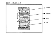
図5は、具体的な半導体装置の設計データのパターン例である。図5は、一例として、セル領域を境界領域(OUTER)と、内部領域(CORE)に分けて示している。また、境界領域(OUTERR)と、内部領域(CORE)との間に、セル補正境界線(BOUNDARY)が示されている。また、セルの最外周(存在領域)として、EXTENTが示されている。 FIG. 5 is a specific pattern example of design data of a semiconductor device. FIG. 5 shows, as an example, a cell region divided into a boundary region (OUTER) and an internal region (CORE). Further, a cell correction boundary line (BOUNDARY) is shown between the boundary region (OUTERR) and the inner region (CORE). Further, EXTENT is shown as the outermost periphery (existing region) of the cell.
図6に設計データのパターン例を示す。この例では、半導体装置内に、IP−M1からIP−M5で示されるセルが配置されている。図6のように、LSIのような半導体装置を記述する設計データは多くのマクロやライブラリと称されるパターン群を集めて構成されている。そのうち本処理システムでパターン分離を行う対象セルは複数存在しえる。一般に、半導体装置の設計データは、セルが自セル内に、他のセルを参照して配置する構造を取る。したがって、セルと、そのセルに参照される他のセルとは、階層構造を有する。そのような階層構造中に、補正対象となる対象セルが存在する。さらに、対象セルの配下にも子セルが存在する。 FIG. 6 shows an example of design data patterns. In this example, cells indicated by IP-M1 to IP-M5 are arranged in the semiconductor device. As shown in FIG. 6, design data describing a semiconductor device such as an LSI is configured by collecting a large number of patterns called macros and libraries. Among them, there may be a plurality of target cells for pattern separation in this processing system. In general, the design data of a semiconductor device has a structure in which a cell is arranged in its own cell with reference to another cell. Therefore, the cell and other cells referred to by the cell have a hierarchical structure. There is a target cell to be corrected in such a hierarchical structure. Further, there are child cells under the target cell.
図7に、図6と同一の設計データの階層構造例とその階層構造に対する処理概要を示す。この半導体装置は、トップセル直下に、BLK_1〜BLK_3、およびRAM_BLKで示される回路ブロックが配置されている。また、BLK_1の下位には、子セルとして、IP_M1が配置されている。IP_M1以下には、さらに、FNC_M1、CELL_M1等の階層が定義されている。BLK_2、BLK_3についても、同様に、下位に、IP_M2、IP_M3、あるいは、IP_M4等を配置している。また、RAM_BLKの下位には、RAM_CELLが通常は、マトリクスで配置される。また、IP_M5は、TOPセル直下に配置されている。なお、ここでは、本処理システムにより、境界領域と、内部領域との分離処理に直接関係のないセルの構造についての説明は省略する。 FIG. 7 shows an example of a hierarchical structure of the same design data as FIG. 6 and an outline of processing for the hierarchical structure. In this semiconductor device, circuit blocks indicated by BLK_1 to BLK_3 and RAM_BLK are arranged immediately below the top cell. Also, IP_M1 is arranged as a child cell below BLK_1. Below IP_M1, layers such as FNC_M1 and CELL_M1 are further defined. Similarly for BLK_2 and BLK_3, IP_M2, IP_M3, IP_M4, and the like are arranged in the lower order. Also, RAM_CELL is usually arranged in a matrix below RAM_BLK. IP_M5 is arranged immediately below the TOP cell. Here, description of the cell structure that is not directly related to the separation process between the boundary area and the internal area by the present processing system is omitted.
図7では、IP_M1を例にして、処理の概要が示されている。処理システムには、例えば、条件ファイル等のパラメータによって、補正対象のセルが、例えば、設計データ(一般には、LSI−CADのインターフェースフォーマット)中のセルを識別する名称(以下、セル名称)で指定される。また、処理システムには、境界領域の幅、すなわち、境界線を発生させるべきセル外周からの寸法が指定される。 FIG. 7 shows an overview of the process using IP_M1 as an example. In the processing system, for example, a cell to be corrected is designated by a name (hereinafter referred to as a cell name) for identifying a cell in design data (generally, an LSI-CAD interface format) by a parameter such as a condition file. Is done. In addition, the width of the boundary region, that is, the dimension from the outer periphery of the cell where the boundary line is to be generated is designated in the processing system.
まず、処理システムは、指定されたセル名称を基に、補正対象のセルであるIP_M1を検索する。処理システムは、該当するセルの設計データを検索し、そのセル内の図形データを抽出する。 First, the processing system searches for IP_M1 that is a correction target cell based on the designated cell name. The processing system searches the design data of the corresponding cell and extracts graphic data in the cell.
次に、処理システムは、指定されて境界領域の幅に基づいて、セル外周から内側に、境界線を発生させる(外周枠発生)。そして、処理システムは、その外周枠で、セルの内のデータを境界領域と、内部領域に分割する。内部領域のデータは、そのまま、基のセルであるIP_M1に残される。一方、境界領域のデータは、新たなセル名称(例えば、WK_IP_M1)が付与され、新たなセルが生成される。生成された新たなセルは、トップセル以下のレイアウトに変更がないように、IP_M1に外接する位置に配置される。 Next, the processing system generates a boundary line from the cell periphery to the inside based on the width of the specified boundary region (peripheral frame generation). Then, the processing system divides the data in the cell into the boundary area and the inner area with the outer peripheral frame. The data in the internal area is left as it is in IP_M1, which is the base cell. On the other hand, a new cell name (for example, WK_IP_M1) is given to the data in the boundary region, and a new cell is generated. The generated new cell is arranged at a position circumscribing IP_M1 so that the layout below the top cell is not changed.
図8に、補正対象のセル(IP_M1からIP_M5)を内部領域と境界領域に分け、さらに、境界領域を新たなセル(WK_IP_M1からWK_IP_M5)として、定義したパターンの例を示す。図8では、理解を容易にするため、境界領域のハッチングパターンを内部領域と異なる種類で示している。 FIG. 8 shows an example of a defined pattern in which cells to be corrected (IP_M1 to IP_M5) are divided into an internal region and a boundary region, and the boundary region is a new cell (WK_IP_M1 to WK_IP_M5). In FIG. 8, for easy understanding, the hatching pattern of the boundary region is shown in a different type from the inner region.
図9は、本処理装置で境界領域と内部領域とに分離した階層構造の例である。この例では、階層構造は大きく2つに分類される。すなわち、補正対象の対象セルを境界領域と、内部領域とに分離した後、トップセル配下にセル補正境界領域を構成する構造(WK_TOP)を付加している。WK_TOP以下には、WK_IP_M1からWK_IP_M5で示される境界領域のデータが配置される。 FIG. 9 shows an example of a hierarchical structure that is separated into a boundary area and an internal area by this processing apparatus. In this example, the hierarchical structure is roughly classified into two. That is, after the target cell to be corrected is separated into a boundary region and an internal region, a structure (WK_TOP) that constitutes the cell correction boundary region is added under the top cell. Below WK_TOP, data of boundary areas indicated by WK_IP_M1 to WK_IP_M5 is arranged.
一方、WK_TOP以外の階層構造は、変更されていない。ただし、補正対象のセル(IP_M1からIP_M5)からは、境界領域が削除され、内部領域を構成する部分を含む構造となっている。 On the other hand, the hierarchical structure other than WK_TOP is not changed. However, the boundary area is deleted from the cells to be corrected (IP_M1 to IP_M5), and the cell has a structure including a part constituting the internal area.
<システム構成>
図10は、本処理システムのパターンデータ処理フローを例示する図である。本処理システムには、設計データ100と条件ファイル101とが入力される。設計データ100には、半導体装置全体を記述する図形データがセルの階層構造で記述されている。一方、条件ファイル101には、処理すべき設計データのファイル名、設計データ中のトップセルの名称、処理対象のレイヤ、トップセル配下のセルのうち、補正対象のセル名、補正の条件、境界領域の幅等が指定される。
<System configuration>
FIG. 10 is a diagram illustrating a pattern data processing flow of the processing system.
本処理システムは、条件ファイル101の指定にしたがって、設計データを読む。そして、本処理システムは、近接効果補正処理の対象レイヤを選択し、対象セルに、セルデータの存在する範囲を特定する外周境界線を設定する。外周境界線は、例えば、セル内の図形データの座標値の最小値(XMIN,YMIN)と最大値(XMAX,YMAX)とによって、矩形を構成する。この外周境界線は、セルの最外周であることを判断するための情報である。さらに、本処理システムは、外周境界線に対してセル補正境界線を設定させる。セル補正境界線は、セルの外部のパターンからの近接効果の影響が及ぶ境界領域と、影響が及ばない内部領域とを分割する線である。このセル補正境界線の位置は、図2に示した光近接効果の影響範囲の測定結果から決定される。
The processing system reads design data in accordance with the specification of the
セル補正境界線を発生させた後、内部領域と境界領域とを分離するためにセルの重なり除去を行い、セル内の階層構造を展開し、セル内をフラットな階層のないデータとする。さらに、本処理システムは、フラットにされたデータを格納しておき、境界線に沿ってパターンを分離する。そして、本処理システムは、補正境界線より内側の内部領域については、そのまま元の階層構造に残す。一方、補正境界線の外側で分離したパターンデータを境界領域のセルとして新たなセル名を付加する。そして、本処理システムは、境界領域のセルをトップセル配下の階層構造に組み込み、階層の再構築を行う。 After the cell correction boundary line is generated, cell overlap removal is performed to separate the internal region and the boundary region, the hierarchical structure in the cell is expanded, and the cell has data without a flat hierarchy. Further, the processing system stores the flattened data and separates the pattern along the boundary line. Then, the present processing system leaves the inner area inside the correction boundary line as it is in the original hierarchical structure. On the other hand, a new cell name is added with the pattern data separated outside the correction boundary line as a cell of the boundary region. The processing system then incorporates the cells in the boundary area into the hierarchical structure under the top cell, and reconstructs the hierarchy.
このとき、トップセルから参照したときの半導体装置のパターン形状自体には変化がないようにする。すなわち、分離された境界領域のセルのパターンは、元の階層構造に残された内部領域のパターンとの距離に変化がない位置に配置されることになる。また、分離前に、内部領域のパターンと接触していた境界領域のセルのパターンは、元の階層構造に残された内部領域のパターンと接触する位置に配置されることになる。このようにして、図9に示したように、トップセル直下で、例えば、WK_TOPのようなセル名が付与され、境界領域のパターンを含むセルであることが明示された階層構造が構築される。この処理の後、内部領域のセルに関しては近接効果補正を施したセルと入れ替え処理をすることも容易に可能となる。 At this time, the pattern shape itself of the semiconductor device when referenced from the top cell is not changed. That is, the cell pattern of the separated boundary region is arranged at a position where there is no change in the distance from the pattern of the inner region left in the original hierarchical structure. In addition, the cell pattern in the boundary area that has been in contact with the pattern in the internal area before the separation is arranged at a position in contact with the pattern in the internal area remaining in the original hierarchical structure. In this way, as shown in FIG. 9, a hierarchical structure is constructed immediately below the top cell, with a cell name such as WK_TOP, for example, that clearly indicates that the cell includes a boundary area pattern. . After this processing, the cells in the inner area can be easily replaced with the cells subjected to the proximity effect correction.
次に、本処理システムは、パターンデータには、分割された近接効果補正処理が実行される。すなわち、本処理システムは、パターンデータ補正処理用の条件ファイル(間隔・
パターン幅・光学的条件)に基づき、最上位階層セルからセル領域単位に各パターンデー
タを確認しながら、個々にパターンデータ補正処理を実施する。その場合に、内部領域のパターンについては、設計データ中で、境界領域を分離前のデータによって、個々に補正すればよい。また、境界領域については、対象セル外部の他のセル(対象セルの内部領域を除外した半導体装置の全データ)とともに、補正処理を実行すればよい(102)。
Next, the processing system executes a divided proximity effect correction process on the pattern data. In other words, the processing system uses a condition file (interval,
Based on the pattern width and optical conditions), the pattern data correction processing is performed individually while checking each pattern data from the highest hierarchical cell in cell area units. In this case, for the pattern of the internal region, the boundary region may be individually corrected with the data before separation in the design data. For the boundary region, correction processing may be executed together with other cells outside the target cell (all data of the semiconductor device excluding the internal region of the target cell) (102).
次に、本処理装置は、パターンデータ補正処理後、フラクチャリング処理し(103)、フォトマスク作成用のパターンデータ(描画データ1014)が作成される。フラクチャリングとは、通常は、多角形で記述された設計データのパターンをマスク描画装置の入力形式の図形(例えば、台形)に分割する処理をいう。また、フラクチャリングでは、パターン間の重なり除去等の処理も実行される。次に、その描画用データをフォトマスク作成用の描画装置に読み込ませ、描画を実施後(105)、フォトマスクができ上がる。 Next, the processing apparatus performs a fracturing process after the pattern data correction process (103), and pattern data (drawing data 1014) for creating a photomask is created. Fracturing usually refers to a process of dividing a design data pattern described in a polygon into figures (for example, trapezoids) in an input format of a mask drawing apparatus. In fracturing, processing such as removal of overlap between patterns is also executed. Next, the drawing data is read into a drawing apparatus for creating a photomask, and after drawing is performed (105), a photomask is completed.
図11に、本処理システムの構成図を例示する。本処理システムは、例えばパーソナルコンピュータやワークステーション等の装置に、コンピュータプログラムを実装することにより実現される。図11の処理システムは、コンピュータ1000とコンピュータ1000に接続されるディスプレイ装置1001、通信装置1002、および入力装置より構成される。入力装置は、例えばキーボード1003およびマウス1004等のポインティングデバイスを含む。
FIG. 11 illustrates a configuration diagram of the processing system. This processing system is realized by mounting a computer program on an apparatus such as a personal computer or a workstation. The processing system in FIG. 11 includes a
本処理システムによるパターンデータ補正処理方法は、コンピュータが実行可能なコンピュータプログラムとして実現される。このコンピュータプログラムは、CPU1006等の演算部と記憶媒体1007やRAM1008等の記憶部を介して、処理を実施する。ROM1009は、コンピュータ1000の基本動作を制御するための制御プログラムおよび本処理システムの機能を実現するコンピュータプログラムが格納されている。このコンピュータプログラムを実行することで、上記説明したたように、半導体装置の設計データに対する補正処理方法を実行し、マスク描画用データを作成する。この補正処理およびマスク描画用データの作成処理を実行する計算機環境が、本処理システムである。
The pattern data correction processing method according to the present processing system is realized as a computer program executable by a computer. This computer program executes processing via a calculation unit such as the
このコンピュータプログラムは、通信装置1002、あるいは、着脱可能な記録媒体(
例えば。DVD)を介して、コンピュータ1000にインストールされる。なお、通信装置1002に接続されるネットワーク、あるいは着脱可能な記録媒体は、作成されたマスク描画用データをマスク描画装置に入力するときの媒体としても使用される。
This computer program is stored in the
For example. Installed on the
<データ処理の詳細手順>
図12Aおよび図12Bに、本処理システムのパターンデータ処理フローを例示する。この処理は、処理システムを構成するコンピュータ1000で実行されるコンピュータプログラムによって実現される。この処理では、本処理システムは、まず、条件ファイル101の指定にしたがって、光近接効果補正の対象レイヤを選択する(S1)。そして、処理システムは、対象レイヤ中の対象領域指定セル中の子セル最外周設定処理を実行する(S2)。ここで、対象領域指定セルとは、本処理対象のセルを子セルとして含む上位セルをいう。対象領域指定セルによって、処理対象のセル群を大枠で指定できる。対象領域指定セルのセル名称は、条件ファイル101に指定される。ここでの処理は、対象領域指定セルに含まれる処理対象の下位セル(以下、子セルともいう)に、それぞれの最外周を示す線(あるいは、矩形領域、第1のセル領域に相当)を設定する処理である。
<Detailed procedure for data processing>
12A and 12B illustrate a pattern data processing flow of the processing system. This process is realized by a computer program executed by the
この処理では、処理システムは、対象領域指定セル中のそれぞれの子セルのパターンの配置を確認する(S21)。すなわち、処理システムは、子セルを1つずつ取り出し、取り出した子セル自体および取り出した子セル以下の階層で定義され、配置されているセル中の図形を定義する座標の最大値と最小値を抽出する。座標の最大値と、最小値は、処理中の子セルの原点を基準した座標系にそれぞれの図形あるいは下位の階層を配置した状態で判定される。そして、処理システムは、図形の座標の最大値(XMAX,YMAX)と最小値(XMIN,YMIN)によって定義される矩形を抽出し、子セルの最外周として登録する(S22)。この処理を実行する処理システムのCPU1006が、第1のセル領域を選択する手段に相当する。
In this process, the processing system confirms the arrangement of each child cell pattern in the target area designation cell (S21). That is, the processing system extracts child cells one by one, and defines the maximum value and the minimum value of the coordinates that define the figure in the arranged cell that is defined in the extracted child cell itself and the hierarchy below the extracted child cell. Extract. The maximum value and the minimum value of the coordinates are determined in a state where each figure or lower layer is arranged in a coordinate system based on the origin of the child cell being processed. Then, the processing system extracts a rectangle defined by the maximum value (XMAX, YMAX) and minimum value (XMIN, YMIN) of the coordinates of the graphic and registers it as the outermost periphery of the child cell (S22). The
次に、処理システムは、対象領域指定セル中のすべての子セルを処理したか否かを判定する(S23)。未処理の子セルが存在する場合には、処理システムは、制御をS21に戻す。一方、S23の判定で、すべての子セルの処理が終了すると、処理システムは、制御をS3に進める。 Next, the processing system determines whether or not all child cells in the target area designation cell have been processed (S23). If there is an unprocessed child cell, the processing system returns the control to S21. On the other hand, when the processing of all the child cells is completed in the determination of S23, the processing system advances the control to S3.
なお、図12Aでは、省略しているが、対象領域指定セルを複数指定することもできる。その場合には、S3の処理の前に、すべての対象領域指定セルに対するする処理が終了したか、否かの判定がなされる。そして、未処理の対象領域指定セルが存在する場合には、制御をS2の先頭に戻し、未処理の対象領域指定セルについて同様の処理を繰り返せばよい。 Although omitted in FIG. 12A, a plurality of target area designation cells can be designated. In that case, before the process of S3, it is determined whether or not the process for all the target area designation cells has been completed. If there is an unprocessed target area designation cell, the control is returned to the head of S2, and the same process may be repeated for the unprocessed target area designation cell.
次に、処理システムは、セル最外周から光近接効果の及ばない寸法によってセル補正境界線を設定する(S3)。この処理では、処理システムは、補正処理の条件ファイル101から、条件を読む(S31)。そして、セル最外周からセル補正境界線までの数値を決定する(S32)。この数値は、例えば、図2のような測定結果にしたがって設定されるべきものである。これによって、セル最外周からセル補正境界線までの境界領域(第1の領域)が確定する。この処理を実行する処理システムのCPU1006が、第1の領域を確定する手段に相当する。なお、セル補正境界線の設定によって、セル補正境界線で囲まれた第2の領域も決定されることになる。
Next, the processing system sets a cell correction boundary line with a dimension that does not reach the optical proximity effect from the outermost periphery of the cell (S3). In this process, the processing system reads the conditions from the correction process condition file 101 (S31). And the numerical value from a cell outermost periphery to a cell correction | amendment boundary line is determined (S32). This numerical value should be set according to the measurement result as shown in FIG. As a result, the boundary region (first region) from the cell outermost periphery to the cell correction boundary line is determined. The
そして、処理システムは、セル最外周から、決定された位置にセル補正境界線を発生させる。そして、処理システムは、セル補正境界線で確定された境界領域(また、セル最外周からセル補正境界線までの境界領域の帯状領域を確定する座標)をファイルに登録する(S34)。 Then, the processing system generates a cell correction boundary line at the determined position from the outermost periphery of the cell. Then, the processing system registers in the file the boundary area determined by the cell correction boundary line (and the coordinates for determining the band-like area of the boundary area from the cell outermost periphery to the cell correction boundary line) (S34).
次に、処理システムは、セル補正境界線での子セルの重なり除去を実行する(S4)。セル補正境界線での子セルの重なり除去とは、子セルおよび子セル配下の階層に位置するセル中で、子セルの上記境界領域と交差するパターンを抽出する処理である。 Next, the processing system executes overlap removal of child cells at the cell correction boundary line (S4). The child cell overlap removal at the cell correction boundary line is a process of extracting a pattern intersecting the boundary region of the child cell in the child cell and the cell located in the hierarchy under the child cell.
この処理では、処理システムは、子セルの境界領域と、子セルのパターンとの関係を認識する(S41)。そして、子セルに設定した上記境界領域と、子セルのパターンとが重なっているか否かを判定する(S42)。重なっていない場合には、そのパターンにはついては、全体が内部領域に含まれることになる。一方、重なっている場合には、そのパターンをセル内の配置位置でフラット化する。このような処理をすべての子セル内のパターンおよび子セル配下のセル中のパターンについて繰り返し、フラット化するパターンを決定する(S43)。そして、S43でフラット化の対象とされたパターンをフラット化し、ファイルにパターンを登録する(S44)。 In this process, the processing system recognizes the relationship between the boundary region of the child cell and the child cell pattern (S41). Then, it is determined whether or not the boundary area set in the child cell overlaps the child cell pattern (S42). If they do not overlap, the entire pattern is included in the internal area. On the other hand, if they overlap, the pattern is flattened at the arrangement position in the cell. Such a process is repeated for all the patterns in the child cells and the patterns in the cells under the child cells, and the pattern to be flattened is determined (S43). Then, the pattern to be flattened in S43 is flattened, and the pattern is registered in the file (S44).
次に、処理システムは、対象セルを分割する(S5)。まず、処理システムは、セル補正境界線の線分を発生する(S51)。そして、発生させたセル境界線でフラット化されているパターンを分割する(S52)。この処理では、例えば、セル補正境界で囲まれた矩形領域(内部領域に相当)と、フラット化されたパターンとのAND演算によって、まず、セル補正境界線より内側に位置するパターンが取得される。そして、フラット化されたパターンから、その取得された内部領域に位置するパターンをサブトラクト(減算)することによって、セル補正境界線より外側に位置するパターンが取得される。 Next, the processing system divides the target cell (S5). First, the processing system generates a line segment of the cell correction boundary line (S51). Then, the flattened pattern is divided by the generated cell boundary line (S52). In this process, for example, a pattern located inside the cell correction boundary line is first acquired by an AND operation of a rectangular area (corresponding to the inner area) surrounded by the cell correction boundary and the flattened pattern. . Then, a pattern positioned outside the cell correction boundary line is acquired by subtracting (subtracting) the pattern positioned in the acquired internal region from the flattened pattern.
そして、処理システムは、セル補正境界線より外側に位置するパターンを境界領域のパターンとして、作業用のファイル(またはメモリ)に登録する(S53)。また、処理システムは、セル補正境界線より内側に位置するパターンを内部領域のパターンとして登録する(S54)。この場合の登録は、基本的には、分割されたパターンのうち、内部領域に存在するパターンを元の子セル(あるいは、子セル配下の階層に存在するセル)に戻す処理である。 Then, the processing system registers the pattern positioned outside the cell correction boundary line as a boundary area pattern in the work file (or memory) (S53). Further, the processing system registers a pattern located inside the cell correction boundary line as a pattern of the internal region (S54). The registration in this case is basically a process of returning the pattern existing in the internal area among the divided patterns to the original child cell (or the cell existing in the hierarchy under the child cell).
次に、処理システムは、階層構造の解析処理を実行する(S6)。ここでは、処理システムは、トップセルから補正対象の対象領域指定セルに至る階層構造を解析する(S61)。階層構造を解析するとは、トップセルから対象領域指定セルに至るまで、順次親子関係を辿り、トップセルの原点での、対象領域指定セルの配置関係を求めることをいう。そして、そして、処理システムは、解析した対象領域指定セルの階層構造をファイル(またはメモリ)に格納する(S62)。この場合、対象領域指定セルには、内部領域のパターンと境界領域のパターンが登録されている。 Next, the processing system executes a hierarchical structure analysis process (S6). Here, the processing system analyzes the hierarchical structure from the top cell to the target area designation cell to be corrected (S61). Analyzing the hierarchical structure means that the parent-child relationship is sequentially traced from the top cell to the target area designated cell, and the arrangement relation of the target area designated cell at the top cell origin is obtained. Then, the processing system stores the analyzed hierarchical structure of the target area designation cell in a file (or memory) (S62). In this case, an internal area pattern and a boundary area pattern are registered in the target area designating cell.
さらに、処理システムは、S53の処理でファイルに登録した境界領域のパターンをセル補正境界領域のセルとしてセル化する。具体的には、新たなセル名を付与する(S63)。 Furthermore, the processing system converts the boundary area pattern registered in the file in the process of S53 into a cell as a cell of the cell correction boundary area. Specifically, a new cell name is assigned (S63).
次に、処理システムは、階層構造を設定する(S7)。この処理を実行するCPU1006が、階層構造を構築する手段に相当する。本処理システムでは、条件ファイル101の指定の指定にしたがって、2種類の階層構造を再構成可能としている。すなわち、処理システムは、セル補正境界領域をトップセル直下に付加すべきか否かを判定する(S71)。条件ファイル101にて、セル補正境界領域をトップセル直下に付加すべき指定がされている場合、トップセル直下に、新たに生成したセル補正境界領域のパターンを含むセルを付加する(S72)。このとき、内部領域については、そのまま対象セルに維持される。
Next, the processing system sets a hierarchical structure (S7). The
一方、条件ファイル101にて、セル補正境界領域をトップセル直下に付加すべき指定がされていない場合、それぞれの対象領域指定セル直下で、内部領域のパターンを含む元のセルの階層構造と、内部領域から分離された子セルの境界領域のパターンを含むセルとが維持される。そして、以上の構造が、新たな設計データとして、登録される(S8)。
On the other hand, if it is not specified in the
なお、ここでは、対象領域指定セルを指定し、その配下の子セルに対して、内部領域と境界領域に分割する処理を実行した。しかし、そのような処理に代えて、内部領域と境界領域に分割する処理対象のセルを直接指定するようにしてもよい。その場合には、図12の処理で、子セルに相当するセルの名称を条件ファイル101に設定できるようにすればよい。
In this case, the process of designating the target area designation cell and dividing the subordinate child cells into the internal area and the boundary area is executed. However, instead of such processing, a processing target cell to be divided into an internal region and a boundary region may be directly designated. In that case, the name of the cell corresponding to the child cell may be set in the
図13に、本処理システムによって階層構造が再構築された設計データに対する光近接効果補正処理を例示する。この処理では、処理システムは、まず、トップセル以下の階層構造から、補正対象のセルを抽出する。補正対象のセルは、通常条件ファイル101に指定されている。そして、本処理システムは、その補正対象のセルの種別を判断する(S100)。セルの種別とは、内部領域に相当するパターンのセルか、境界領域のパターンのセルかをいう。そして、本処理システムは、その判定にしたがって(S101)、それぞれの種別ごとに補正処理を実行する。
FIG. 13 illustrates an optical proximity effect correction process for design data whose hierarchical structure has been reconstructed by this processing system. In this process, the processing system first extracts a correction target cell from the hierarchical structure below the top cell. The correction target cell is specified in the
すなわち、内部領域のパターンを含むセルについては、セルライブラリから、境界領域を分割する前のセルのパターンを抽出する(S102)。境界領域を分割する前のセルのパターンが必要となるのは、内部領域のパターンについて、光近接効果補正を実行するためには、境界領域を含む対象セル全体のパターンが必要となるからである。 That is, for the cell including the pattern of the inner area, the cell pattern before dividing the boundary area is extracted from the cell library (S102). The pattern of the cell before dividing the boundary area is necessary because the pattern of the entire target cell including the boundary area is required to perform the optical proximity correction on the pattern of the inner area. .
そして、処理システムは、対象セル全体のパターンについて、単独で光近接効果補正を実行する(S103)。この処理を実行するCPU1006が、第1のセル領域のパターンに基づいて近接効果補正を行う手段に相当する。なお、光近接効果補正(OPC)とは、露光、現像の物理モデルに基づくシミュレーションによって光近接効果(OPE)を予測し、その予測値に基づきマスクパターン補正量を割り出し、レチクル作成用のデータ上でパターンの辺を移動し、あるいはパターン形状を変更する処理である。このようなデータ上の補正により、半導体基板上に形成されるパターン形状が設計形状からずれる現象を抑制する。
And a processing system performs optical proximity effect correction | amendment independently about the pattern of the whole object cell (S103). The
光近接効果補正では、予め求めておいた補正ルール(OPCルール)に基づき設計パターンの補正を行うルールベースOPCと、リソグラフィープロセスにおける現象をモデル化したシミュレータにより設計パターンの補正を行うモデルベースOPCを対象層に応じて使い分ける。 In the optical proximity correction, a rule-based OPC that corrects a design pattern based on a correction rule (OPC rule) that has been obtained in advance, and a model-based OPC that corrects a design pattern using a simulator that models a phenomenon in a lithography process. Use properly according to the target layer.
ルールベースOPCの手段としては、まず、種々の図形処理を組み合わせた補正ルールを実験などで作成しておく。具体的には、一対のラインパターンに対して、線幅又は隣接スペース寸法に基づいて線幅を狭めたり又は広げたりする変更量のルールである。このルールを基にライン補正を行う。また、ラインパターンの先端が細く転写(パターニング)されることを防ぐために、ラインパターンの先端に矩形図形を付加するハンマーヘッド補正を行う。また、方形状パターンのコーナー部分が後退した状態でパターニングされることを防ぐために、方形状パターンの凸型コーナー部に矩形を付加するセリフ補正を行う。またL字状パターンの凹型コーナーが太った状態でパターニングされることを防ぐために、凹型コーナーに削り込みを施すインセット補正を行う。 As a rule-based OPC means, first, a correction rule in which various graphic processes are combined is created through experiments or the like. Specifically, it is a rule of a change amount for narrowing or widening the line width based on the line width or the adjacent space dimension with respect to a pair of line patterns. Line correction is performed based on this rule. In order to prevent the tip of the line pattern from being finely transferred (patterned), hammerhead correction is performed to add a rectangular figure to the tip of the line pattern. In addition, in order to prevent patterning in a state in which the corner portion of the square pattern is receded, serif correction for adding a rectangle to the convex corner portion of the square pattern is performed. In order to prevent the L-shaped pattern from being patterned with a thick concave corner, inset correction is performed to cut the concave corner.
モデルベースOPCは、オリジナルの設計データを元に、マスクパターンと転写された半導体基板上のパターンとの差異をシミュレーションによって計算して、設計データ通り
の形状が得られるように、パターンデータの辺を移動する。
Model-based OPC calculates the difference between the mask pattern and the transferred pattern on the semiconductor substrate based on the original design data by simulation, and sets the sides of the pattern data so that the shape as the design data is obtained. Moving.
次に、対象セルから内部領域を抽出し、設計データ中の対象セルのデータと入れ替える(S104)。なお、対象セルから内部領域を抽出するには、セル補正境界線で囲まれた矩形領域と、近接効果補正後のパターンとのAND演算を実行すればよい。 Next, an internal region is extracted from the target cell and replaced with the data of the target cell in the design data (S104). In order to extract the internal region from the target cell, an AND operation between the rectangular region surrounded by the cell correction boundary line and the pattern after proximity effect correction may be executed.
一方、境界領域のパターンを含むセルについては、設計データ中の周辺パターンとマージ(合成)する(S105)。ここで、周辺パターンとは、対象セルの外部に隣接するセルのパターンをいう。例えば、単純な処理では、内部領域のパターンを含むセルを除去し、残りのデータをフラットに展開することによって周辺パターンを得ることができる。そして、周辺パターンを含む境界領域のパターンに光近接効果補正を実行する(S106)。この処理を実行するCPU1006が、第1の領域に含まれるパターンと前記第1のセル領域の周囲に配置されるパターンとの関係から近接効果補正を行う手段に相当する。
On the other hand, the cell including the pattern of the boundary region is merged (synthesized) with the peripheral pattern in the design data (S105). Here, the peripheral pattern refers to a pattern of cells adjacent to the outside of the target cell. For example, in a simple process, a peripheral pattern can be obtained by removing cells including the pattern of the inner region and developing the remaining data flat. Then, optical proximity effect correction is performed on the pattern of the boundary area including the peripheral pattern (S106). The
次に、処理システムは、すべての補正対象セルに対する処理が終了したか否かを判定する(S107)。未処理の補正対象セルが残っている場合、処理システムは、制御をS100に戻す。一方、すべての補正対象セルに対する処理が終了した場合、処理システムは、内部領域と、周辺パターンと合成された境界領域のパターンとを合成する(S108)。その後、図10に示したフラクチャリング103を実行すればよい。 Next, the processing system determines whether or not the processing for all the correction target cells has been completed (S107). If an unprocessed correction target cell remains, the processing system returns the control to S100. On the other hand, when the processing for all the correction target cells is completed, the processing system combines the inner region and the pattern of the boundary region combined with the peripheral pattern (S108). Thereafter, the fracturing 103 shown in FIG. 10 may be executed.
<マスク製造システムの構成>
図14に、本処理システムを含む、マスク製造システムの構成を例示する。まず、本処理システムで処理の対象とされた設計データは、LSI−CAD E1で作成される。設計データは、ネットワークまたは着脱可能な記録媒体を通じて、処理システム(パターンデータ処理システムE2)に引き渡され、図12に示した処理が実行される。なお、LSI−CAD E1と、処理システム(パターンデータ処理システムE2)とが、同一のコンピュータ上で実現されてもよい。
<Configuration of mask manufacturing system>
FIG. 14 illustrates a configuration of a mask manufacturing system including the present processing system. First, design data to be processed by this processing system is created by LSI-CAD E1. The design data is delivered to the processing system (pattern data processing system E2) through the network or a removable recording medium, and the processing shown in FIG. 12 is executed. The LSI-CAD E1 and the processing system (pattern data processing system E2) may be realized on the same computer.
次に、処理システムで図12の処理が実行された設計データは、マスク描画装置の描画用データに変換され(図10のフラクチャリング103)、マスク描画装置に引き渡される。なお、本処理システムが、マスク描画装置に付属する制御用コンピュータと一体ものでもよい。その場合には、図10のフラクチャリング103は、マスク描画装置に付属する制御用コンピュータで実行されてもよい。 Next, the design data for which the processing of FIG. 12 has been executed by the processing system is converted into drawing data for the mask drawing apparatus (fracturing 103 in FIG. 10) and delivered to the mask drawing apparatus. The present processing system may be integrated with a control computer attached to the mask drawing apparatus. In that case, the fracturing 103 in FIG. 10 may be executed by a control computer attached to the mask drawing apparatus.
そして、マスク描画装置E3では、描画用データを基に、遮光部で被覆されさらにレジストが塗布されたガラス基板が電子ビーム、あるいはレーザー等で露光される。描画後、レジストが現像設備E4で現像される。これによって、パターンに該当する部分(またはパターン以外の部分)のレジストが除去される。 In the mask drawing apparatus E3, based on the drawing data, the glass substrate coated with a light shielding portion and coated with a resist is exposed with an electron beam or a laser. After drawing, the resist is developed by the development facility E4. Thereby, the resist corresponding to the pattern (or a part other than the pattern) is removed.
さらに、現像されたレジストをマスクとするエッチングがエッチング装置E5で実行される。これによって、現像によってレジストが除去された個所から、遮光部が除去され、透明なガラスが露出し、パターンに該当する部分(またはパターン以外の部分)での光の透過が可能となる。 Further, etching using the developed resist as a mask is performed by the etching apparatus E5. Thus, the light shielding portion is removed from the portion where the resist is removed by development, the transparent glass is exposed, and light can be transmitted through a portion corresponding to the pattern (or a portion other than the pattern).
次に、レジスト剥離装置E6によって、ガラス基板上に残っているレジストが除去される。さらに、洗浄装置E7で、ガラス基板が洗浄され、マスク上でのパターン形成が終了する。なお、場合によっては、遮光部とガラス表面とによってパターンが形成された基板全体に、異物付着防止のための透明薄膜(ペリクル膜)を添付してもよい。 Next, the resist remaining on the glass substrate is removed by the resist stripping device E6. Further, the glass substrate is cleaned by the cleaning device E7, and the pattern formation on the mask is completed. In some cases, a transparent thin film (pellicle film) for preventing foreign matter adhesion may be attached to the entire substrate on which a pattern is formed by the light shielding portion and the glass surface.
以上述べたように、本実施形態の処理システムによれば、光近接効果補正等の補正処理
の対象となる対象セルをセル外のパターンの影響の及ぶ範囲と、及ばない範囲とに分割する。そして、セル外のパターンの影響の及ぶ範囲については、セル外の周辺パターンともに、補正処理を実行する。また、セル外のパターンの影響の及ばない範囲ついて、セル単独で、光近接効果補正を実行する。このようにすることで、セル外のパターンの影響の及ばない範囲について、セルの規則性を維持した上で、光近接効果補正を実行できる。
As described above, according to the processing system of this embodiment, a target cell that is a target of correction processing such as optical proximity correction is divided into a range that is affected by a pattern outside the cell and a range that is not. Then, for the range affected by the pattern outside the cell, the correction process is executed together with the peripheral pattern outside the cell. In addition, the optical proximity effect correction is executed in the cell alone for a range that is not affected by the pattern outside the cell. By doing so, the optical proximity effect correction can be executed while maintaining the regularity of the cell in the range not affected by the pattern outside the cell.
ここで、セルの規則性を維持するとは、例えば、同一のセルが多数回繰り返して参照して配置されている場合、その配置された構造を維持することをいう。例えば、セルの内部領域に関しては、光近接効果補正を実行しても、補正後に同一のパターンが得られるので、多数回繰り返して参照して配置された状態を維持できる。一方、境界領域部分については、補正対象のセルの外部に隣接するセルに依存してパターンが変形されることになる。 Here, maintaining the regularity of a cell means, for example, maintaining the arranged structure when the same cell is repeatedly referenced and arranged many times. For example, with respect to the inner region of the cell, even if the optical proximity effect correction is performed, the same pattern can be obtained after the correction, so that it is possible to maintain the state of being repeatedly referenced and arranged many times. On the other hand, for the boundary region portion, the pattern is deformed depending on the cell adjacent to the outside of the correction target cell.
ただし、図3に示したような階層構造に再構成することによって、対象セルの外部のセルが変更になった場合でも、容易に光近接効果補正を実行できる。したがって、例えば、同一のセルを異なる品種のLSIに組み込んだ場合でも、セル外のパターンの影響の及ばない範囲ついては、すでに実施済みの近接効果補正の結果をそのまま利用できる。また、セルに繰り返しの規則性がある場合には、その規則性を維持できる。 However, by reconfiguring the hierarchical structure as shown in FIG. 3, the optical proximity effect correction can be easily executed even when the cell outside the target cell is changed. Therefore, for example, even when the same cell is incorporated in an LSI of a different type, the proximity effect correction result that has already been performed can be used as it is for a range that is not affected by the pattern outside the cell. Further, when a cell has repeated regularity, the regularity can be maintained.
一方、境界領域部分については、上記図13のS105,S106と同様の手順で、補正対象のセルの外部に隣接するセルとともに、近接効果補正を実行すればよい。したがって、セルの境界部分に限定して周辺パターンの影響を反映した近接効果補正を実行すればよく、再度近接効果補正を実行する場合も、極めて効率よく、計算機資源を節約でき、すべてのパターンを考慮した近接効果補正よりも短い処理時間で処理を完了できる。 On the other hand, for the boundary region portion, proximity effect correction may be executed together with cells adjacent to the outside of the correction target cell in the same procedure as S105 and S106 in FIG. Therefore, it is only necessary to execute proximity effect correction that reflects the influence of the surrounding pattern limited to the cell boundary, and even when proximity effect correction is performed again, it is extremely efficient and can save computer resources and save all patterns. Processing can be completed in a shorter processing time than the proximity effect correction that has been considered.
100 設計データ
101 条件ファイル
102 パターンデータ補正
103 フラクチャリング
104 描画データ
105 フォトマスク露光
106 フォトマスク
1000 コンピュータ
1001 ディスプレイ
1002 通信装置
1003 キーボード
1004 マウス
1005 インターフェース
1006 CPU
1007 記憶媒体
1008 RAM
1009 ROM
DESCRIPTION OF
1007
1009 ROM
Claims (7)
前記第1のセル領域の周囲に配置されるパターンにより前記第1のセル領域のパターン形状が影響を受ける第1の領域を画定する工程と、
前記第1のセル領域内であって、前記第1の領域以外の領域を第2の領域とする工程と、
前記第1の領域と前記第2の領域を各々のセル領域とする階層構造を構築する工程と、
前記第1の領域内において、第1の領域に含まれるパターンと前記第1のセル領域の周囲に配置されるパターンとの関係から近接効果補正を行う工程と、
前記第2の領域内において、前記第1のセル領域のパターンに基づいて近接効果補正を行う工程と、を実行するフォトマスクデータの処理方法。 Selecting a first cell region in the design data having a hierarchical structure;
Demarcating a first region in which a pattern shape of the first cell region is affected by a pattern arranged around the first cell region;
A step of setting a region other than the first region in the first cell region as a second region;
Constructing a hierarchical structure in which each of the first region and the second region is a cell region;
In the first region, performing a proximity effect correction from the relationship between the pattern included in the first region and the pattern disposed around the first cell region;
And a step of performing proximity effect correction based on a pattern of the first cell region in the second region.
前記階層構造を構築する工程では、前記第2の領域は、前記第1の領域が含まれる第1の階層構造と分岐して前記トップセルから参照される分岐セルとして配置される請求項1から3のいずれか1項に記載のフォトマスクデータの処理方法。 The hierarchical structure has a hierarchical structure of a top cell and a lower cell referenced from the top cell,
In the step of constructing the hierarchical structure, the second area is arranged as a branch cell that branches from the first hierarchical structure including the first area and is referenced from the top cell. 4. The photomask data processing method according to any one of items 3.
前記階層構造を構築する工程は、前記第1の領域が含まれる第1の階層構造と分岐して前記トップセルから参照される分岐セルとして配置するか否かの指定の有無を判定する工
程と、
前記第2の領域を前記トップセルから参照される分岐セルとして配置する指定がある場合に、前記トップセルから参照される分岐セルのセル名を付与して、第2の領域を前記トップセル内に配置する工程と、を有する請求項1から3のいずれか1項に記載のフォトマスクデータの処理方法。 The hierarchical structure has a hierarchical structure of a top cell and a lower cell referenced from the top cell,
The step of building the hierarchical structure includes a step of determining whether or not it is specified whether to branch from the first hierarchical structure including the first region and to arrange as a branch cell referenced from the top cell; ,
When there is a designation to arrange the second area as a branch cell referenced from the top cell, a cell name of the branch cell referenced from the top cell is given, and the second area is included in the top cell. The method for processing photomask data according to any one of claims 1 to 3, further comprising the step of:
前記第1のセル領域の周囲に隣接するパターンにより前記第1のセル領域のパターン形状が影響を受ける第1の領域を画定する手段と、
前記第1のセル領域内であって、前記第1の領域以外の領域を第2の領域とする手段と、
前記第1の領域と前記第2の領域を各々のセル領域とする階層構造を構築する手段と、
前記第1の領域内において、第1の領域に含まれるパターンと前記第1のセル領域の周囲に配置されるパターンとの関係から近接効果補正を行う手段と、
前記第2の領域内において、前記第1のセル領域のパターンに基づいて近接効果補正を行う手段と、を備えるフォトマスクデータ処理システム。 Means for selecting a first cell region in design data having a hierarchical structure;
Means for defining a first region in which a pattern shape of the first cell region is affected by a pattern adjacent to the periphery of the first cell region;
Means for setting a region other than the first region in the first cell region as a second region;
Means for constructing a hierarchical structure in which each of the first region and the second region is a cell region;
Means for performing proximity effect correction from the relationship between the pattern included in the first region and the pattern disposed around the first cell region in the first region;
A photomask data processing system comprising: means for performing proximity effect correction based on a pattern of the first cell region in the second region.
前記第1のセル領域の周囲に隣接する第1のパターンにより前記第1のセル領域のパターン形状が影響を受ける第1の領域を画定する工程と、
前記第1のセル領域内であって、前記第1の領域以外の領域を第2の領域とする工程と、
前記第1の領域と前記第2の領域を各々のセル領域とする階層構造を構築する工程と、
前記第1の領域内において、第1の領域に含まれるパターンと前記第1のセル領域の周囲に配置されるパターンとの関係から近接効果補正を行う工程と、
前記第2の領域内において、前記第1のセル領域のパターンに基づいて近接効果補正を行う工程と、
前記近接効果補正後の第1のセル領域を含む設計データからフォトマスク作成用のパターンデータを作成する工程と、
前記パターンデータに基づいてフォトマスクを作成する工程と、を実行するフォトマスク製造方法。 Selecting a first cell region in the design data having a hierarchical structure;
Demarcating a first region in which a pattern shape of the first cell region is affected by a first pattern adjacent to the periphery of the first cell region;
A step of setting a region other than the first region in the first cell region as a second region;
Constructing a hierarchical structure in which each of the first region and the second region is a cell region;
In the first region, performing a proximity effect correction from the relationship between the pattern included in the first region and the pattern disposed around the first cell region;
In the second region, performing proximity effect correction based on the pattern of the first cell region;
Creating pattern data for photomask creation from design data including the first cell region after the proximity effect correction;
And a step of creating a photomask based on the pattern data.
Priority Applications (2)
| Application Number | Priority Date | Filing Date | Title |
|---|---|---|---|
| JP2008060118A JP5309623B2 (en) | 2008-03-10 | 2008-03-10 | Photomask data processing method, photomask data processing system, and manufacturing method using hierarchical structure |
| US12/401,252 US8141006B2 (en) | 2008-03-10 | 2009-03-10 | Photomask data processing method, photomask data processing system and manufacturing method |
Applications Claiming Priority (1)
| Application Number | Priority Date | Filing Date | Title |
|---|---|---|---|
| JP2008060118A JP5309623B2 (en) | 2008-03-10 | 2008-03-10 | Photomask data processing method, photomask data processing system, and manufacturing method using hierarchical structure |
Publications (2)
| Publication Number | Publication Date |
|---|---|
| JP2009216936A JP2009216936A (en) | 2009-09-24 |
| JP5309623B2 true JP5309623B2 (en) | 2013-10-09 |
Family
ID=41054929
Family Applications (1)
| Application Number | Title | Priority Date | Filing Date |
|---|---|---|---|
| JP2008060118A Expired - Fee Related JP5309623B2 (en) | 2008-03-10 | 2008-03-10 | Photomask data processing method, photomask data processing system, and manufacturing method using hierarchical structure |
Country Status (2)
| Country | Link |
|---|---|
| US (1) | US8141006B2 (en) |
| JP (1) | JP5309623B2 (en) |
Families Citing this family (5)
| Publication number | Priority date | Publication date | Assignee | Title |
|---|---|---|---|---|
| JP5024141B2 (en) * | 2008-03-21 | 2012-09-12 | 富士通セミコンダクター株式会社 | Pattern data creation method, program for creating the pattern data, and medium containing the program |
| FR2993374A1 (en) * | 2012-07-12 | 2014-01-17 | St Microelectronics Crolles 2 | METHOD FOR PRODUCING A PHOTOLITHOGRAPHY MASK |
| US10810339B1 (en) * | 2016-12-23 | 2020-10-20 | Synopsys, Inc. | Determination of dimensional changes of features across mask pattern simulation fields |
| CN111458974B (en) * | 2020-05-23 | 2023-06-23 | 珠海市睿晶聚源科技有限公司 | Method and system for accelerating layout processing |
| KR20230081361A (en) * | 2021-11-30 | 2023-06-07 | 삼성전자주식회사 | Full-chip cell CD(Critical Dimension) correction method, and mask manufacturing method comprising the correction method |
Family Cites Families (37)
| Publication number | Priority date | Publication date | Assignee | Title |
|---|---|---|---|---|
| JP2830330B2 (en) * | 1989-04-04 | 1998-12-02 | 松下電器産業株式会社 | Proximity effect correction method |
| EP1023640B1 (en) | 1997-09-17 | 2013-07-03 | Synopsys, Inc. | Data hierarchy layout correction and verification method and apparatus |
| US6453452B1 (en) * | 1997-12-12 | 2002-09-17 | Numerical Technologies, Inc. | Method and apparatus for data hierarchy maintenance in a system for mask description |
| WO1999014636A1 (en) | 1997-09-17 | 1999-03-25 | Numerical Technologies, Inc. | Method and apparatus for data hierarchy maintenance in a system for mask description |
| US6425113B1 (en) * | 2000-06-13 | 2002-07-23 | Leigh C. Anderson | Integrated verification and manufacturability tool |
| JP2002229179A (en) * | 2001-02-07 | 2002-08-14 | Nec Microsystems Ltd | Optical proximity correction method |
| US6505327B2 (en) * | 2001-04-13 | 2003-01-07 | Numerical Technologies, Inc. | Generating an instance-based representation of a design hierarchy |
| US6668367B2 (en) * | 2002-01-24 | 2003-12-23 | Nicolas B. Cobb | Selective promotion for resolution enhancement techniques |
| US6813758B2 (en) * | 2002-03-14 | 2004-11-02 | Lsi Logic Corporation | Optical proximity correction driven hierarchy |
| US6931613B2 (en) * | 2002-06-24 | 2005-08-16 | Thomas H. Kauth | Hierarchical feature extraction for electrical interaction calculations |
| US6807663B2 (en) * | 2002-09-23 | 2004-10-19 | Numerical Technologies, Inc. | Accelerated layout processing using OPC pre-processing |
| US7093228B2 (en) * | 2002-12-20 | 2006-08-15 | Lsi Logic Corporation | Method and system for classifying an integrated circuit for optical proximity correction |
| JP3993545B2 (en) | 2003-09-04 | 2007-10-17 | 株式会社東芝 | Pattern manufacturing method, semiconductor device manufacturing method, pattern manufacturing system, cell library, and photomask manufacturing method |
| US7533363B2 (en) * | 2004-03-29 | 2009-05-12 | Takumi Technology Corporation | System for integrated circuit layout partition and extraction for independent layout processing |
| US7669158B2 (en) * | 2004-09-30 | 2010-02-23 | Cadence Design Systems, Inc. | Method and system for semiconductor design hierarchy analysis and transformation |
| JP2007080965A (en) * | 2005-09-12 | 2007-03-29 | Matsushita Electric Ind Co Ltd | Semiconductor device manufacturing method, library used therefor, recording medium, and semiconductor manufacturing apparatus |
| US20080250374A1 (en) * | 2005-09-20 | 2008-10-09 | Freescale Semiconductor, Inc. | Method of Making an Integrated Circuit |
| JP2007086587A (en) | 2005-09-26 | 2007-04-05 | Renesas Technology Corp | Mask pattern design method and semiconductor device manufacturing method |
| JP2007199234A (en) * | 2006-01-25 | 2007-08-09 | Fujitsu Ltd | Photomask design method and design apparatus |
| JP2007280200A (en) * | 2006-04-10 | 2007-10-25 | Elpida Memory Inc | Layout pattern data correction apparatus and correction method |
| US7360199B2 (en) * | 2006-05-26 | 2008-04-15 | International Business Machines Corporation | Iterative method for refining integrated circuit layout using compass optical proximity correction (OPC) |
| JP2008020751A (en) * | 2006-07-13 | 2008-01-31 | National Institute Of Advanced Industrial & Technology | Mask pattern design method and semiconductor device manufacturing method using the same |
| KR100831271B1 (en) * | 2006-08-16 | 2008-05-22 | 동부일렉트로닉스 주식회사 | How to change physical layout data through programmatic creation of physical layer |
| WO2008023660A1 (en) * | 2006-08-25 | 2008-02-28 | National Institute Of Advanced Industrial Science And Technology | Mask pattern designing method and semiconductor device manufacturing method using the same |
| US8056022B2 (en) * | 2006-11-09 | 2011-11-08 | Mentor Graphics Corporation | Analysis optimizer |
| US7650587B2 (en) * | 2006-11-30 | 2010-01-19 | International Business Machines Corporation | Local coloring for hierarchical OPC |
| US20080168419A1 (en) * | 2007-01-04 | 2008-07-10 | International Business Machines Corporation | Optical proximity correction improvement by fracturing after pre-optical proximity correction |
| US7926002B2 (en) * | 2007-02-28 | 2011-04-12 | Mentor Graphics Corporation | Selective optical proximity layout design data correction |
| US7669175B2 (en) * | 2007-05-11 | 2010-02-23 | International Business Machines Corporation | Methodology to improve turnaround for integrated circuit design using geometrical hierarchy |
| US8099685B2 (en) * | 2007-07-31 | 2012-01-17 | Mentor Graphics Corporation | Model based microdevice design layout correction |
| US7647569B2 (en) * | 2007-08-01 | 2010-01-12 | Micron Technology, Inc. | Systems, methods, and computer-readable media for adjusting layout database hierarchies for more efficient database processing and storage |
| US8214775B2 (en) * | 2007-09-14 | 2012-07-03 | Luminescent Technologies, Inc. | System for determining repetitive work units |
| US8191017B2 (en) * | 2008-01-14 | 2012-05-29 | Mentor Graphics Corp. | Site selective optical proximity correction |
| US7984395B2 (en) * | 2008-01-17 | 2011-07-19 | Synopsys, Inc. | Hierarchical compression for metal one logic layer |
| US7937682B2 (en) * | 2008-01-31 | 2011-05-03 | Synopsys, Inc. | Method and apparatus for automatic orientation optimization |
| US7865864B2 (en) * | 2008-02-01 | 2011-01-04 | International Business Machines Corporation | Electrically driven optical proximity correction |
| JP5024141B2 (en) * | 2008-03-21 | 2012-09-12 | 富士通セミコンダクター株式会社 | Pattern data creation method, program for creating the pattern data, and medium containing the program |
-
2008
- 2008-03-10 JP JP2008060118A patent/JP5309623B2/en not_active Expired - Fee Related
-
2009
- 2009-03-10 US US12/401,252 patent/US8141006B2/en not_active Expired - Fee Related
Also Published As
| Publication number | Publication date |
|---|---|
| US20090228860A1 (en) | 2009-09-10 |
| JP2009216936A (en) | 2009-09-24 |
| US8141006B2 (en) | 2012-03-20 |
Similar Documents
| Publication | Publication Date | Title |
|---|---|---|
| JP3934719B2 (en) | Optical proximity correction method | |
| US6560766B2 (en) | Method and apparatus for analyzing a layout using an instance-based representation | |
| JP4999013B2 (en) | Integrated OPC verification tool | |
| US6470489B1 (en) | Design rule checking system and method | |
| US6668367B2 (en) | Selective promotion for resolution enhancement techniques | |
| US7657864B2 (en) | System and method for integrated circuit device design and manufacture using optical rule checking to screen resolution enhancement techniques | |
| KR101450500B1 (en) | Computer-implemented methods, carrier media, and systems for creating a metrology target structure design for a reticle layout | |
| JP4510118B2 (en) | Optical proximity effect correction method and apparatus, optical proximity effect verification method and apparatus, exposure mask manufacturing method, optical proximity effect correction program, and optical proximity effect verification program | |
| US8359562B2 (en) | System and method for semiconductor device fabrication using modeling | |
| CN100520597C (en) | Method and system for optical proximity correction | |
| JP5052625B2 (en) | Method and program for designing mask layout | |
| TWI398906B (en) | Data generation method for semiconductor device, and electron beam exposure system | |
| WO2005040917A2 (en) | System and method for lithography simulation | |
| JP5024141B2 (en) | Pattern data creation method, program for creating the pattern data, and medium containing the program | |
| US8234596B2 (en) | Pattern data creating method, pattern data creating program, and semiconductor device manufacturing method | |
| JP5309623B2 (en) | Photomask data processing method, photomask data processing system, and manufacturing method using hierarchical structure | |
| JP2010156866A (en) | Feature-quantity extracting method, test pattern selecting method, resist model creating method, and designed-circuit-pattern verifying method | |
| JP2015108671A (en) | Pattern creation method | |
| US8990755B2 (en) | Defective artifact removal in photolithography masks corrected for optical proximity | |
| JP6338368B2 (en) | Method for evaluating pattern optical image | |
| US20090293038A1 (en) | Method and correction apparatus for correcting process proximity effect and computer program product | |
| TWI597561B (en) | Method for generating pattern, method for manufacturing mask, exposure method, method for manufacturing semiconductor device, storage medium, and information processing apparatus | |
| JPH11327120A (en) | Light intensity simulation apparatus, light intensity simulation method, and recording medium recording light intensity simulation program | |
| JP2011176046A (en) | Exposure method and method of making semiconductor device | |
| JP4006013B2 (en) | Optical proximity correction method |
Legal Events
| Date | Code | Title | Description |
|---|---|---|---|
| A621 | Written request for application examination |
Free format text: JAPANESE INTERMEDIATE CODE: A621 Effective date: 20101126 |
|
| A977 | Report on retrieval |
Free format text: JAPANESE INTERMEDIATE CODE: A971007 Effective date: 20120525 |
|
| A131 | Notification of reasons for refusal |
Free format text: JAPANESE INTERMEDIATE CODE: A131 Effective date: 20120529 |
|
| A521 | Written amendment |
Free format text: JAPANESE INTERMEDIATE CODE: A523 Effective date: 20120730 |
|
| TRDD | Decision of grant or rejection written | ||
| A01 | Written decision to grant a patent or to grant a registration (utility model) |
Free format text: JAPANESE INTERMEDIATE CODE: A01 Effective date: 20130604 |
|
| A61 | First payment of annual fees (during grant procedure) |
Free format text: JAPANESE INTERMEDIATE CODE: A61 Effective date: 20130617 |
|
| R150 | Certificate of patent or registration of utility model |
Free format text: JAPANESE INTERMEDIATE CODE: R150 |
|
| S531 | Written request for registration of change of domicile |
Free format text: JAPANESE INTERMEDIATE CODE: R313531 |
|
| R350 | Written notification of registration of transfer |
Free format text: JAPANESE INTERMEDIATE CODE: R350 |
|
| LAPS | Cancellation because of no payment of annual fees |