JP5283922B2 - Magnetic memory - Google Patents
Magnetic memory Download PDFInfo
- Publication number
- JP5283922B2 JP5283922B2 JP2008033400A JP2008033400A JP5283922B2 JP 5283922 B2 JP5283922 B2 JP 5283922B2 JP 2008033400 A JP2008033400 A JP 2008033400A JP 2008033400 A JP2008033400 A JP 2008033400A JP 5283922 B2 JP5283922 B2 JP 5283922B2
- Authority
- JP
- Japan
- Prior art keywords
- magnetic recording
- magnetic
- magnetization
- layer
- magnetic field
- Prior art date
- Legal status (The legal status is an assumption and is not a legal conclusion. Google has not performed a legal analysis and makes no representation as to the accuracy of the status listed.)
- Expired - Fee Related
Links
- 230000005291 magnetic effect Effects 0.000 title claims abstract description 598
- 230000015654 memory Effects 0.000 title claims abstract description 107
- 230000005415 magnetization Effects 0.000 claims abstract description 309
- 239000000696 magnetic material Substances 0.000 claims description 17
- 239000000463 material Substances 0.000 claims description 17
- 230000005294 ferromagnetic effect Effects 0.000 claims 3
- 230000004888 barrier function Effects 0.000 description 49
- 238000004088 simulation Methods 0.000 description 38
- 230000000694 effects Effects 0.000 description 29
- 230000000052 comparative effect Effects 0.000 description 24
- 238000002834 transmittance Methods 0.000 description 19
- 238000000034 method Methods 0.000 description 14
- 238000002347 injection Methods 0.000 description 13
- 239000007924 injection Substances 0.000 description 13
- PXHVJJICTQNCMI-UHFFFAOYSA-N Nickel Chemical compound [Ni] PXHVJJICTQNCMI-UHFFFAOYSA-N 0.000 description 12
- 230000004048 modification Effects 0.000 description 12
- 238000012986 modification Methods 0.000 description 12
- 230000005290 antiferromagnetic effect Effects 0.000 description 9
- 230000008859 change Effects 0.000 description 9
- BASFCYQUMIYNBI-UHFFFAOYSA-N platinum Chemical compound [Pt] BASFCYQUMIYNBI-UHFFFAOYSA-N 0.000 description 9
- KDLHZDBZIXYQEI-UHFFFAOYSA-N Palladium Chemical compound [Pd] KDLHZDBZIXYQEI-UHFFFAOYSA-N 0.000 description 8
- 229910004298 SiO 2 Inorganic materials 0.000 description 8
- 230000007246 mechanism Effects 0.000 description 8
- CPLXHLVBOLITMK-UHFFFAOYSA-N magnesium oxide Inorganic materials [Mg]=O CPLXHLVBOLITMK-UHFFFAOYSA-N 0.000 description 7
- 239000000395 magnesium oxide Substances 0.000 description 7
- AXZKOIWUVFPNLO-UHFFFAOYSA-N magnesium;oxygen(2-) Chemical compound [O-2].[Mg+2] AXZKOIWUVFPNLO-UHFFFAOYSA-N 0.000 description 7
- 239000011159 matrix material Substances 0.000 description 7
- 239000011651 chromium Substances 0.000 description 6
- 229910017052 cobalt Inorganic materials 0.000 description 6
- 239000010941 cobalt Substances 0.000 description 6
- GUTLYIVDDKVIGB-UHFFFAOYSA-N cobalt atom Chemical compound [Co] GUTLYIVDDKVIGB-UHFFFAOYSA-N 0.000 description 6
- 230000009977 dual effect Effects 0.000 description 6
- 239000010931 gold Substances 0.000 description 6
- 239000002131 composite material Substances 0.000 description 5
- 239000010949 copper Substances 0.000 description 5
- 238000000605 extraction Methods 0.000 description 5
- 239000010419 fine particle Substances 0.000 description 5
- 229910052804 chromium Inorganic materials 0.000 description 4
- 239000011572 manganese Substances 0.000 description 4
- 229910052759 nickel Inorganic materials 0.000 description 4
- 229910052697 platinum Inorganic materials 0.000 description 4
- 239000004065 semiconductor Substances 0.000 description 4
- 239000000758 substrate Substances 0.000 description 4
- 238000012546 transfer Methods 0.000 description 4
- VYZAMTAEIAYCRO-UHFFFAOYSA-N Chromium Chemical compound [Cr] VYZAMTAEIAYCRO-UHFFFAOYSA-N 0.000 description 3
- 229910003321 CoFe Inorganic materials 0.000 description 3
- XEEYBQQBJWHFJM-UHFFFAOYSA-N Iron Chemical compound [Fe] XEEYBQQBJWHFJM-UHFFFAOYSA-N 0.000 description 3
- 230000009471 action Effects 0.000 description 3
- 230000002238 attenuated effect Effects 0.000 description 3
- 229910052802 copper Inorganic materials 0.000 description 3
- 230000005684 electric field Effects 0.000 description 3
- 238000010894 electron beam technology Methods 0.000 description 3
- 238000005530 etching Methods 0.000 description 3
- 238000010438 heat treatment Methods 0.000 description 3
- 239000012212 insulator Substances 0.000 description 3
- 229910052763 palladium Inorganic materials 0.000 description 3
- 238000000992 sputter etching Methods 0.000 description 3
- 229910018072 Al 2 O 3 Inorganic materials 0.000 description 2
- 229910019236 CoFeB Inorganic materials 0.000 description 2
- RYGMFSIKBFXOCR-UHFFFAOYSA-N Copper Chemical compound [Cu] RYGMFSIKBFXOCR-UHFFFAOYSA-N 0.000 description 2
- PWHULOQIROXLJO-UHFFFAOYSA-N Manganese Chemical compound [Mn] PWHULOQIROXLJO-UHFFFAOYSA-N 0.000 description 2
- 229910045601 alloy Inorganic materials 0.000 description 2
- 239000000956 alloy Substances 0.000 description 2
- 230000015572 biosynthetic process Effects 0.000 description 2
- 230000008878 coupling Effects 0.000 description 2
- 238000010168 coupling process Methods 0.000 description 2
- 238000005859 coupling reaction Methods 0.000 description 2
- 239000003302 ferromagnetic material Substances 0.000 description 2
- 229910052737 gold Inorganic materials 0.000 description 2
- 239000011810 insulating material Substances 0.000 description 2
- 239000011777 magnesium Substances 0.000 description 2
- 229910052748 manganese Inorganic materials 0.000 description 2
- 239000000203 mixture Substances 0.000 description 2
- 230000035699 permeability Effects 0.000 description 2
- 230000004044 response Effects 0.000 description 2
- 239000010948 rhodium Substances 0.000 description 2
- 229910052707 ruthenium Inorganic materials 0.000 description 2
- 229910052715 tantalum Inorganic materials 0.000 description 2
- 239000010936 titanium Substances 0.000 description 2
- 230000005641 tunneling Effects 0.000 description 2
- 239000013598 vector Substances 0.000 description 2
- KRHYYFGTRYWZRS-UHFFFAOYSA-M Fluoride anion Chemical compound [F-] KRHYYFGTRYWZRS-UHFFFAOYSA-M 0.000 description 1
- FYYHWMGAXLPEAU-UHFFFAOYSA-N Magnesium Chemical compound [Mg] FYYHWMGAXLPEAU-UHFFFAOYSA-N 0.000 description 1
- KJTLSVCANCCWHF-UHFFFAOYSA-N Ruthenium Chemical compound [Ru] KJTLSVCANCCWHF-UHFFFAOYSA-N 0.000 description 1
- XUIMIQQOPSSXEZ-UHFFFAOYSA-N Silicon Chemical compound [Si] XUIMIQQOPSSXEZ-UHFFFAOYSA-N 0.000 description 1
- 229910003087 TiOx Inorganic materials 0.000 description 1
- RTAQQCXQSZGOHL-UHFFFAOYSA-N Titanium Chemical compound [Ti] RTAQQCXQSZGOHL-UHFFFAOYSA-N 0.000 description 1
- 229910007667 ZnOx Inorganic materials 0.000 description 1
- 229910007746 Zr—O Inorganic materials 0.000 description 1
- 229910052782 aluminium Inorganic materials 0.000 description 1
- XAGFODPZIPBFFR-UHFFFAOYSA-N aluminium Chemical compound [Al] XAGFODPZIPBFFR-UHFFFAOYSA-N 0.000 description 1
- PNEYBMLMFCGWSK-UHFFFAOYSA-N aluminium oxide Inorganic materials [O-2].[O-2].[O-2].[Al+3].[Al+3] PNEYBMLMFCGWSK-UHFFFAOYSA-N 0.000 description 1
- 229910000808 amorphous metal alloy Inorganic materials 0.000 description 1
- 238000000137 annealing Methods 0.000 description 1
- 230000006399 behavior Effects 0.000 description 1
- 230000008901 benefit Effects 0.000 description 1
- 239000002772 conduction electron Substances 0.000 description 1
- 239000000470 constituent Substances 0.000 description 1
- 239000011258 core-shell material Substances 0.000 description 1
- 239000013078 crystal Substances 0.000 description 1
- 238000013016 damping Methods 0.000 description 1
- 230000007423 decrease Effects 0.000 description 1
- 230000000593 degrading effect Effects 0.000 description 1
- 238000013461 design Methods 0.000 description 1
- 230000006866 deterioration Effects 0.000 description 1
- 230000002542 deteriorative effect Effects 0.000 description 1
- 238000010586 diagram Methods 0.000 description 1
- 238000009792 diffusion process Methods 0.000 description 1
- 238000005516 engineering process Methods 0.000 description 1
- 230000005284 excitation Effects 0.000 description 1
- 238000002474 experimental method Methods 0.000 description 1
- 230000005293 ferrimagnetic effect Effects 0.000 description 1
- 230000006870 function Effects 0.000 description 1
- 229910052733 gallium Inorganic materials 0.000 description 1
- PCHJSUWPFVWCPO-UHFFFAOYSA-N gold Chemical compound [Au] PCHJSUWPFVWCPO-UHFFFAOYSA-N 0.000 description 1
- 230000003993 interaction Effects 0.000 description 1
- 230000002452 interceptive effect Effects 0.000 description 1
- 229910052741 iridium Inorganic materials 0.000 description 1
- GKOZUEZYRPOHIO-UHFFFAOYSA-N iridium atom Chemical compound [Ir] GKOZUEZYRPOHIO-UHFFFAOYSA-N 0.000 description 1
- 229910052749 magnesium Inorganic materials 0.000 description 1
- 230000005389 magnetism Effects 0.000 description 1
- 238000004949 mass spectrometry Methods 0.000 description 1
- 229910052751 metal Inorganic materials 0.000 description 1
- 239000002184 metal Substances 0.000 description 1
- 229910052750 molybdenum Inorganic materials 0.000 description 1
- 229910052758 niobium Inorganic materials 0.000 description 1
- 150000004767 nitrides Chemical class 0.000 description 1
- 230000003287 optical effect Effects 0.000 description 1
- 239000002245 particle Substances 0.000 description 1
- 238000000059 patterning Methods 0.000 description 1
- 238000000206 photolithography Methods 0.000 description 1
- 230000010287 polarization Effects 0.000 description 1
- 230000008569 process Effects 0.000 description 1
- 238000002310 reflectometry Methods 0.000 description 1
- 229910052703 rhodium Inorganic materials 0.000 description 1
- MHOVAHRLVXNVSD-UHFFFAOYSA-N rhodium atom Chemical compound [Rh] MHOVAHRLVXNVSD-UHFFFAOYSA-N 0.000 description 1
- VSZWPYCFIRKVQL-UHFFFAOYSA-N selanylidenegallium;selenium Chemical compound [Se].[Se]=[Ga].[Se]=[Ga] VSZWPYCFIRKVQL-UHFFFAOYSA-N 0.000 description 1
- 229910052710 silicon Inorganic materials 0.000 description 1
- 239000010703 silicon Substances 0.000 description 1
- 230000007480 spreading Effects 0.000 description 1
- 238000004544 sputter deposition Methods 0.000 description 1
- GUVRBAGPIYLISA-UHFFFAOYSA-N tantalum atom Chemical compound [Ta] GUVRBAGPIYLISA-UHFFFAOYSA-N 0.000 description 1
- JBQYATWDVHIOAR-UHFFFAOYSA-N tellanylidenegermanium Chemical compound [Te]=[Ge] JBQYATWDVHIOAR-UHFFFAOYSA-N 0.000 description 1
- 238000012360 testing method Methods 0.000 description 1
- HLLICFJUWSZHRJ-UHFFFAOYSA-N tioxidazole Chemical compound CCCOC1=CC=C2N=C(NC(=O)OC)SC2=C1 HLLICFJUWSZHRJ-UHFFFAOYSA-N 0.000 description 1
- 229910052719 titanium Inorganic materials 0.000 description 1
- 229910052723 transition metal Inorganic materials 0.000 description 1
- 229910052721 tungsten Inorganic materials 0.000 description 1
- LEONUFNNVUYDNQ-UHFFFAOYSA-N vanadium atom Chemical compound [V] LEONUFNNVUYDNQ-UHFFFAOYSA-N 0.000 description 1
- 229910052725 zinc Inorganic materials 0.000 description 1
- 239000011701 zinc Substances 0.000 description 1
Images


Classifications
-
- G—PHYSICS
- G11—INFORMATION STORAGE
- G11B—INFORMATION STORAGE BASED ON RELATIVE MOVEMENT BETWEEN RECORD CARRIER AND TRANSDUCER
- G11B25/00—Apparatus characterised by the shape of record carrier employed but not specific to the method of recording or reproducing, e.g. dictating apparatus; Combinations of such apparatus
- G11B25/04—Apparatus characterised by the shape of record carrier employed but not specific to the method of recording or reproducing, e.g. dictating apparatus; Combinations of such apparatus using flat record carriers, e.g. disc, card
-
- G—PHYSICS
- G11—INFORMATION STORAGE
- G11C—STATIC STORES
- G11C11/00—Digital stores characterised by the use of particular electric or magnetic storage elements; Storage elements therefor
- G11C11/02—Digital stores characterised by the use of particular electric or magnetic storage elements; Storage elements therefor using magnetic elements
- G11C11/16—Digital stores characterised by the use of particular electric or magnetic storage elements; Storage elements therefor using magnetic elements using elements in which the storage effect is based on magnetic spin effect
- G11C11/161—Digital stores characterised by the use of particular electric or magnetic storage elements; Storage elements therefor using magnetic elements using elements in which the storage effect is based on magnetic spin effect details concerning the memory cell structure, e.g. the layers of the ferromagnetic memory cell
-
- G—PHYSICS
- G11—INFORMATION STORAGE
- G11C—STATIC STORES
- G11C11/00—Digital stores characterised by the use of particular electric or magnetic storage elements; Storage elements therefor
- G11C11/02—Digital stores characterised by the use of particular electric or magnetic storage elements; Storage elements therefor using magnetic elements
- G11C11/16—Digital stores characterised by the use of particular electric or magnetic storage elements; Storage elements therefor using magnetic elements using elements in which the storage effect is based on magnetic spin effect
- G11C11/165—Auxiliary circuits
- G11C11/1659—Cell access
-
- G—PHYSICS
- G11—INFORMATION STORAGE
- G11C—STATIC STORES
- G11C11/00—Digital stores characterised by the use of particular electric or magnetic storage elements; Storage elements therefor
- G11C11/02—Digital stores characterised by the use of particular electric or magnetic storage elements; Storage elements therefor using magnetic elements
- G11C11/16—Digital stores characterised by the use of particular electric or magnetic storage elements; Storage elements therefor using magnetic elements using elements in which the storage effect is based on magnetic spin effect
- G11C11/165—Auxiliary circuits
- G11C11/1675—Writing or programming circuits or methods
Landscapes
- Engineering & Computer Science (AREA)
- Computer Hardware Design (AREA)
- Mram Or Spin Memory Techniques (AREA)
- Hall/Mr Elements (AREA)
Abstract
Description
本発明は、磁気メモリに関し、特に書き込み電流とともに高周波磁界を印加する磁気メモリに関する。 The present invention relates to a magnetic memory, and more particularly to a magnetic memory that applies a high-frequency magnetic field together with a write current.
従来、磁性体の磁化方向を制御するために、磁界を印加する方法は知られている。例えば、ハードディスクドライブ(HDD:Hard Disk Drive)においては、記録ヘッドから発生する磁界によって媒体の磁化方向を反転させて書き込みを行っている。また、従来型の磁気ランダムアクセスメモリでは、磁気抵抗効果素子の近傍に設けられた配線に電流を流すことで生じる電流磁界をメモリセルに印加することで、メモリセルの磁化方向を制御している。これらの外部磁界による磁化方向を制御する方式(電流磁界書き込み方式ともいう)は古い歴史があり、確立された技術である。 Conventionally, a method of applying a magnetic field to control the magnetization direction of a magnetic material is known. For example, in a hard disk drive (HDD), writing is performed by reversing the magnetization direction of a medium by a magnetic field generated from a recording head. In the conventional magnetic random access memory, the magnetization direction of the memory cell is controlled by applying a current magnetic field generated by flowing a current to a wiring provided in the vicinity of the magnetoresistive effect element to the memory cell. . These methods for controlling the magnetization direction by an external magnetic field (also called current magnetic field writing method) have an old history and are established techniques.
一方、昨今のナノテクノロジーの進歩によって磁性材料の顕著な微細化が可能となり、磁化制御をナノスケールで局所的に行う必要が出てきた。しかしながら、磁界は根本的には空間に広がる性質を有するため、局所化が難しい。特定のビットやメモリセルを選択してその磁化方向を制御させる場合に、ビットやメモリセルのサイズが微小化するのに伴い、隣のビットやメモリセルにまで磁界が及んでしまう「クロストーク」の問題が顕著となる。また、磁界を局所化させるために磁界発生源を小さくすると、磁化方向を制御するのに十分な発生磁界が得られないという問題が生じる。 On the other hand, recent advances in nanotechnology have enabled remarkable miniaturization of magnetic materials, and it has become necessary to locally control magnetization at the nanoscale. However, it is difficult to localize the magnetic field because it has the property of spreading in space. When a specific bit or memory cell is selected and its magnetization direction is controlled, the magnetic field reaches the adjacent bit or memory cell as the size of the bit or memory cell becomes smaller. The problem becomes prominent. Further, if the magnetic field generation source is made small in order to localize the magnetic field, there arises a problem that a generated magnetic field sufficient to control the magnetization direction cannot be obtained.
これを解決する技術として、磁性体に電流を流すことにより磁化反転を起こす「スピン注入磁化反転現象」が知られている(例えば、非特許文献1)。この非特許文献1に記載された技術は、磁気抵抗効果素子に書き込み電流としてのスピン注入電流を流し、そこで発生するスピン偏極された電子を用いて、磁気記録層の磁化を反転させる。具体的には、スピン偏極された電子の角運動量が、磁気記録層としての磁性材料内の電子に伝達されることにより磁気記録層の磁化が反転する。
As a technique for solving this, there is known a “spin injection magnetization reversal phenomenon” in which magnetization reversal is caused by passing a current through a magnetic material (for example, Non-Patent Document 1). The technique described in Non-Patent
このような電流を直接駆動することによる磁化反転技術(スピン注入磁化反転技術)を用いれば、磁化状態をナノスケールで局所的に制御し易くなり、さらに、磁性材料の微細化に応じてスピン注入電流の値も小さくすることができる。このことは、高記録密度のハードディスクドライブや磁気ランダムアクセスメモリなどのスピンエレクトロニクスデバイスの実現に向けての手助けとなる。 By using a magnetization reversal technique (spin injection magnetization reversal technique) by directly driving such a current, it becomes easier to control the magnetization state locally at the nanoscale, and spin injection is performed in accordance with the miniaturization of magnetic materials. The current value can also be reduced. This helps to realize spin electronics devices such as high recording density hard disk drives and magnetic random access memories.
また、ビット線もしくはワード線に交流電流を流し、交流磁界を発生させる磁気記録装置が知られている(例えば、特許文献1)。特許文献1に記載された磁気記録装置は、行線(ビット線)と列線(ワード線)とによってアドレス指定可能な磁気セルがマトリックス状に配列された磁気記録装置である。各磁気セルは、強磁性体からなる磁化固着層/トンネルバリア層/強磁性体からなる磁化自由層(磁気記録層)の積層構造を有する磁気抵抗効果素子を有し、電流の向きに応じて記録を行う。各磁気セルにおいては、上記磁気抵抗効果素子に直列接続されたスイッチング素子(トランジスタ)が備えられている。各磁気セルの磁気抵抗効果素子は1つのビット線に接続されており、各スイッチング素子(トランジスタ)は1つのワード線に接続されている。さらに、記録時に直流電流を流すための直流電源と、交流磁界を発生させるための交流電源と、を有している。
非特許文献1に記載された技術は、書き込み電流のパルス幅が短くなると、磁化反転の有無、つまり磁化反転のバラツキ、が発生するという問題があった(例えば、非特許文献2参照)。これを防ぐためには、書き込み電流をより大きくする必要がある。書き込み電流を大きくすると、磁気抵抗効果素子内で発生する熱の影響で、磁気抵抗効果素子の特性が劣化するなどの信頼性の問題が発生する。また、スピン注入磁化反転を用いた磁気メモリにおいては、書き込み電流が大きくなると選択トランジスタを小さくできなくなり、大容量化が困難になるといった問題がある。当然ながら、磁気記録装置における消費電力が増大することは問題となる。
The technique described in
また、特許文献1に記載された磁気記録装置においては、記録を行うときに必要となる数GHz以上の高周波電流をビット線もしくはワード線に供給しても、十分な高周波透過率で交流電流を流すことが容易ではないという問題があった。
Further, in the magnetic recording device described in
本発明は、上記事情を考慮してなされたものであって、スピン注入による磁化反転の際に、磁化反転のバラツキを小さくしかつ反転電流を低減することのできる磁気メモリを提供することを目的とする。 The present invention has been made in view of the above circumstances, and an object of the present invention is to provide a magnetic memory capable of reducing variation in magnetization reversal and reducing reversal current when reversing magnetization by spin injection. And
本発明の第1の態様による磁気メモリは、磁化の向きが固着された第1磁化固着層、スピン偏極された電流が流れることによって磁化の向きが可変の磁気記録層、および前記第1磁化固着層と前記磁気記録層との間に設けられた第1非磁性層を有する磁気記録素子と、前記磁気記録素子上に設けられ、高周波電流が流れることによって発生する高周波磁界を前記磁気記録層の磁化容易軸と略直交する方向に作用させる高周波電流磁界用配線と、前記高周波電流磁界用配線に対して、前記磁気記録素子と反対側に設けられたグランド線と、を含むメモリセルを備えていることを特徴とする。 The magnetic memory according to the first aspect of the present invention includes a first magnetization pinned layer in which the magnetization direction is fixed, a magnetic recording layer in which the magnetization direction is variable by a spin-polarized current, and the first magnetization A magnetic recording element having a first nonmagnetic layer provided between the pinned layer and the magnetic recording layer; and a high-frequency magnetic field which is provided on the magnetic recording element and is generated when a high-frequency current flows. A memory cell comprising: a high-frequency current magnetic field wiring that acts in a direction substantially perpendicular to the axis of easy magnetization; and a ground line provided on the opposite side of the magnetic recording element with respect to the high-frequency current magnetic field wiring. It is characterized by.
また、本発明の第2の態様による磁気メモリは、磁化の向きが固着された第1磁化固着層、スピン偏極された電流が流れることによって磁化の向きが可変の磁気記録層、および前記第1磁化固着層と前記磁気記録層との間に設けられた第1非磁性層を有する磁気記録素子と、ビット線と、前記ビット線に対して前記磁気記録素子と反対側に、前記ビット線の延在する方向と略直交する方向に延在する高周波電流磁界用配線と、前記高周波電流磁界用配線に対して、前記磁気記録素子と反対側に設けられたグランド線と、を含むメモリセルを備えていることを特徴とする。 The magnetic memory according to the second aspect of the present invention includes a first magnetization pinned layer in which the magnetization direction is fixed, a magnetic recording layer in which the magnetization direction is variable by a spin-polarized current, and the first A magnetic recording element having a first nonmagnetic layer provided between one magnetization pinned layer and the magnetic recording layer; a bit line; and the bit line opposite to the magnetic recording element with respect to the bit line. A high-frequency current magnetic field wiring extending in a direction substantially orthogonal to the direction in which the magnetic recording element extends, and a ground line provided on the opposite side of the magnetic recording element with respect to the high-frequency current magnetic field wiring It is characterized by having.
本発明によれば、スピン注入による磁化反転の際に、磁化反転のバラツキを小さくしかつ反転電流を低減することの可能な磁気メモリを提供することができる。 According to the present invention, it is possible to provide a magnetic memory capable of reducing variation in magnetization reversal and reducing reversal current during magnetization reversal by spin injection.
以下、本発明の実施形態について図面を参照しつつ説明する。なお、各図面中、同様の構成要素には同一の符号を付して詳細な説明は適宜省略する。 Embodiments of the present invention will be described below with reference to the drawings. In addition, in each drawing, the same code | symbol is attached | subjected to the same component and detailed description is abbreviate | omitted suitably.
(第1実施形態)
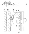
本発明の第1実施形態による磁気メモリを図1に示す。本実施形態の磁気メモリは、マトリクス状に配列された複数のメモリセルを有し、各メモリセルは、磁気記録素子1と、高周波電流磁界用配線30(以下、RF電流磁界用配線ともいう)と、グランド配線35と、引き出し電極40と、接続プラグ45と、スイッチング素子50とを備えている。
(First embodiment)
A magnetic memory according to a first embodiment of the present invention is shown in FIG. The magnetic memory of this embodiment has a plurality of memory cells arranged in a matrix, and each memory cell has a
磁気記録素子1は、磁気抵抗効果素子であって、スピンモーメントが固着された磁性膜を含む磁化固着層2と、非磁性バリア層4と、スピンモーメントが可変の磁気記録層となる磁化自由層6と、がこの順に積層された積層構造を有している。この積層構造は、MTJ(Magnetic Tunnel Junction)などと呼ばれている。本実施形態においては、磁化固着層2は、スピンモーメント(磁化)が上記第1磁性膜の膜面に対して略垂直な方向を向いてスピンモーメントの向きが固定されている。また、磁気記録層6は、スピンモーメントが上記磁性膜のスピンモーメントの向きと平行(同じ向き)または反平行(逆の向き)となる。すなわち、磁気記録層6は、その磁化容易軸が上記磁性膜の膜面に略垂直な方向であり、スピンモーメントの方向が磁化容易軸方向となっている。
The
非磁性バリア層4と反対側の磁化固着層2の面が引き出し電極40と電気的に接続されている。また、非磁性バリア層4と反対側の磁気記録層6の面がビット線20と電気的に接続されている。なお、ビット線20は、同じ行に配列されている複数のメモリセルに対して共通となっている。
The surface of the magnetization pinned
RF電流磁界用配線30は、ビット線20に対して磁気記録素子1と反対側に、ビット線20の延在する方向と略直交する方向に延在するように設けられ、ビット線20との間に設けられる絶縁膜(図示せず)によってビット線20とは電気的に絶縁されている。したがって、RF電流磁界用配線に極性が一定の高周波電流を流すと、この高周波電流によって生じる電流磁界は、磁気記録層6の磁化容易軸と略直交する方向(磁化困難軸方向)に作用することなる。このRF電流磁界用配線30は、このRF電流磁界用配線30に流れる高周波電流による電流磁界が磁気記録層6の磁化容易軸と略直交する方向に作用すれば、何処に配置されていてもよい。
The RF current
グランド線35は、RF電流磁界用配線30に対してビット線20と反対側に、RF電流磁界用配線30と所定の距離dだけ離間して設けられている。そして、グランド線35はRF電流磁界用配線30との間に設けられる絶縁膜(図示せず)によってRF電流磁界用配線30とは電気的に絶縁されている。
The
スイッチング素子50は、MOSトランジスタ50であって半導体基板52に離間して形成されたソース/ドレイン領域54a、54bと、ソース領域54aとドレイン領域54bとの間のチャネルとなる半導体基板52の領域53上に形成されたゲート絶縁膜56と、このゲート絶縁膜56上に形成されたゲート電極58と、備えている。ソース領域54aは、プラグ45を介して引き出し電極40と電気的に接続されている。ドレイン領域54bは、配線65を介して図示しない書き込み回路または読み出し回路に接続されている。すなわち、本実施形態においては、スイッチング素子50は磁気記録素子1と直列に接続された構成となっている。したがって、ビット線20から磁気記録素子1、引き出し電極40、接続プラグ45、スイッチング素子50、および配線65を介して書き込み回路または読み出し回路に電流を流すことができるとともに、これと反対方向に電流を流すことができる。また、ゲート電極58はワード線60と電気的に接続されている。同一の列に配列されたメモリセルのスイッチング素子50のゲート電極58は、同じワード線60と電気的に接続される。スイッチング素子50のONはゲート58に接続されているワード線60により行う。
The
磁化固着層2は図示しない反強磁性層を、磁化固着層に隣接して設けることにより、磁化を強固に固着することも可能となる。磁化固着層2および磁気記録層6は、それぞれ単一の磁性膜からなっていてよいが、非磁性膜を介して互いに強磁性結合または反強磁性結合した磁性膜の積層構造であってもよい。例えば、磁性膜/非磁性膜/磁性膜の3層積層構造や、磁性膜/非磁性膜/磁性膜/非磁性膜/磁性膜の5層積層構造であってもよい。また、非磁性バリア層4は、非磁性の抵抗が高い絶縁材料や半導体からなる。
The magnetization pinned
本実施形態における磁気記録素子は、電子電流25を、磁気記録層6と磁化固着層2との間に流すことによって、磁気記録層6の磁化の方向を制御することができる。具体的には、電子電流25の流れる向き(極性)を変えることで磁気記録層6の磁化の向きを反転させることができる。情報を記録させる場合には、磁気記録層6の磁化の方向に応じて、「0」と「1」とをそれぞれ割り当てればよい。
The magnetic recording element in the present embodiment can control the direction of magnetization of the
本実施形態に係るRF電流磁界用配線30およびグランド線35の形状について説明する。RF電流磁界用配線30のグランド線35と対向する面の幅をW1、グランド線35のRF電流磁界用配線30と対向する面の幅をW2、RF電流磁界用配線30の高さをH1、グランド線35の高さをH2、RF電流磁界用配線30とグランド線35との間のギャップをdとするとこれらの関係はH1≧d≧W1/10、H2≧d≧W2/10を満たすことが望ましい。H1≧dは、RF電流磁界用配線がグランド線と干渉せずにカップリングする上限値であり、d≧W1/10は下限値である。さらに、2×(H1+d)≦H2であることが望ましい。電気力線の広がりとしてグランド線がRF電流磁界用配線の反対側の端からの距離の2倍程度まで網羅すると、ほとんどの電気力線を吸収することができる。また、d<500μmであることが望ましい。500μmは、間に挟まれる誘電体の誘電率と利用する高周波の帯域から電極間のカップリングが効率よく行われる上限値である。このようにすることで、RF電流磁界用配線30に高周波電流を通すと、磁気記録素子(MTJ)に交流磁界を印加し、磁気記録層の磁化の反転を、より低い電流で行うができる。
The shapes of the RF current
次に、磁気記録素子の書き込み、読み出しの動作原理を説明する。 Next, the operation principle of writing and reading of the magnetic recording element will be described.
まず、磁気記録素子における「書き込み」の基本的なメカニズムについて図2(a)、2(b)を参照して説明する。図2(a)は、磁化固着層2から磁気記録層6に向かって、通常の電流とは逆向きとなる電子電流25を流した場合、図2(b)は、磁気記録層6から磁化固着層2に向かって電子電流25を流した場合の模式的断面図である。
First, the basic mechanism of “writing” in the magnetic recording element will be described with reference to FIGS. 2 (a) and 2 (b). 2A shows a case where an electron current 25 having a direction opposite to a normal current flows from the magnetization fixed
磁化固着層2および磁気記録層6の膜面を横切るように電子電流25を流して、磁気記録層6に対する書き込みを行うメカニズムは、以下のように説明される。非磁性バリア層4を介した磁気抵抗効果が、ノーマルタイプである場合について説明する。ここで、「ノーマルタイプ」の磁気抵抗効果とは、非磁性バリア層4の両側の磁性層、すなわち本実施形態では、磁化固着層2と磁気記録層6の磁化が平行の時よりも反平行の時に電気抵抗が高くなる場合をいう。つまり、ノーマルタイプの場合、非磁性バリア層4を介した磁化固着層2と磁気記録層6との間の電気抵抗は、磁化固着層2と磁気記録層6の磁化が平行な時には反平行の時よりも低くなる。
The mechanism for writing to the
まず、図2(a)において、膜面に対して略垂直方向の磁化12を有する磁化固着層2を通過した電子は、磁化12と同じ方向のスピンをもつようになり、これが磁気記録層6へ流れると、このスピンのもつ角運動量が磁気記録層6へ伝達され、磁気記録層6の磁化14に作用する。いわゆるスピントランスファトルクが、磁気記録層6の磁化に働くことになる。これにより、磁気記録層6は、磁化固着層2の磁化12と同じ向き(図2(a)において上向き)の磁化14を持つことになる。この向き(図2(a)おいて上向き)の磁化14を有する磁気記録層6に、例えばデータ「0」を割り当てる。すなわち磁気記録層6の磁化の向きと磁化固着層2の磁化の向きが平行の時にデータ「0」を割り当てる。
First, in FIG. 2A, electrons that have passed through the magnetization pinned
また、図2(b)は、電子電流25の向きを反転させた場合、すなわち磁気記録層6から磁化固着層2に向かって電子電流25を流した場合を示している。磁気記録層6から非磁性バリア層4を通過した電子において、磁化固着層2の磁化12と同じ向き(図2(b)において上向き)のスピンをもった電子は磁化固着層2を通過するが、磁化12と逆向き(図2(b)において下向き)のスピンをもった電子は磁化固着層2と非磁性バリア層4との界面において反射される。この反射された電子のスピンの角運動量が磁気記録層6へ伝達され、磁化14に作用する。これにより、磁気記録層6は磁化12と逆向き(図2(b)において下向き)の磁化14を持つことになる。いわゆるスピントランスファトルクが、磁気記録層6の磁化に働くことになる。この向き(図2(b)おいて下向き)の磁化14を有する磁気記録層30に、例えばデータ「1」を割り当てる。すなわち磁気記録層6の磁化の向きと磁化固着層2の磁化の向きが反平行の時にデータ「1」を割り当てる。なお、図2(a)、2(b)において、符号16は、RF電流磁界用配線30によって発生する電流磁界を示している。
FIG. 2B shows the case where the direction of the electron current 25 is reversed, that is, the case where the electron current 25 flows from the
上述のような作用によって磁気記録層6の磁化の向きが決定され、この磁化の向きに対応してデータ「0」とデータ「1」とが適宜割り当てられて、磁気記録素子における「書き込み」が完了する。以上、非磁性バリア層4を介した磁化固着層2と磁気記録層6との間の磁気抵抗効果が「ノーマルタイプ」の場合について説明した。
The magnetization direction of the
磁気抵抗効果が「リバースタイプ」の場合は、非バリア層4の両側の磁性層の磁化が反平行の時よりも平行の時に電気抵抗が高くなる場合をいう。つまり、リバースタイプの場合、非磁性バリア層4を介した磁化固着層2と磁気記録層6との間の電気抵抗は、磁化固着層2と磁気記録層6の磁化が平行な時には反平行な時よりも高くなる。これによって、磁化固着層2を通過した電子は、磁化12と逆向きのスピンを持つようになる。また、磁化12と同じ向きのスピンを持った電子は反射され、磁化12と逆向きのスピンを持った電子は磁化固着層2を通過することになる。以下の「書き込み」のメカニズムは、磁気抵抗効果が「ノーマルタイプ」の場合と同様であるため、詳細な説明は省略する。
When the magnetoresistive effect is “reverse type”, the electrical resistance is higher when the magnetizations of the magnetic layers on both sides of the
次に、磁気記録素子における「読み出し」のメカニズムについて、図3(a)、3(b)を参照して説明する。図3(a)は、磁化固着層2の磁化12の向きと、磁気記録層6の磁化14の向きが平行の時に、データを読み出すためのセンス電流26を流した場合を示し、図3(b)は、磁化固着層2の磁化12の向きと、磁気記録層6の磁化14の向きが反平行の時に、データを読み出すためのセンス電流26を流した場合を示す断面図である。
Next, the mechanism of “reading” in the magnetic recording element will be described with reference to FIGS. FIG. 3A shows a case where a sense current 26 for reading data is passed when the direction of the
本実施形態に係る磁気記録素子において、磁気記録層6の磁化14の方向の検出は、各層の磁化の相対的な向きにより電気抵抗が変わる「磁気抵抗効果」を利用して行うことができる。すなわち、磁気抵抗効果を利用する場合、磁化固着層2と磁気記録層4との間でセンス電流26を流し、磁気抵抗を測定すればよい。センス電流26の電流値は、記録時に流す電子電流25の電流値よりも小さい。
In the magnetic recording element according to the present embodiment, the direction of the
図3(a)に示す状態の磁気記録素子においては、センス電流26を流して検出される磁気抵抗は、ノーマルタイプの磁気抵抗効果において相対的に小さな値となり、リバースタイプの磁気抵抗効果においては、相対的に大きな値となる。これと反対に、図3(b)に示す状態の磁気記録素子においては、センス電流26を流して検出される磁気抵抗は、ノーマルタイプの磁気抵抗効果において相対的に大きな値となり、リバースタイプの磁気抵抗効果においては相対的に小さな値となる。これら抵抗が互いに異なる状態に、それぞれデータ「0」とデータ「1」を対応づけることにより、2値データの記録読み出しが可能となる。なお、センス電流26の向きは、図3に示した矢印方向と逆向き(図において下から上への向き)にしてもよい。 In the magnetic recording element in the state shown in FIG. 3A, the magnetoresistance detected by flowing the sense current 26 becomes a relatively small value in the normal type magnetoresistance effect, and in the reverse type magnetoresistance effect. A relatively large value. On the other hand, in the magnetic recording element in the state shown in FIG. 3B, the magnetoresistance detected by flowing the sense current 26 becomes a relatively large value in the normal type magnetoresistance effect, and the reverse type The magnetoresistive effect is a relatively small value. By associating data “0” and data “1” with these resistances different from each other, binary data can be recorded and read. The direction of the sense current 26 may be opposite to the arrow direction shown in FIG. 3 (from the bottom to the top in the figure).
次に、第1実施形態による磁気メモリの動作原理について説明する。 Next, the operating principle of the magnetic memory according to the first embodiment will be described.
まず、本実施形態における磁気メモリの記録時の動作について説明する。本実施形態の磁気メモリにおいては、電子電流25が図1において磁化固着層2から磁気記録層6へ(図1において下から上へ)流れる場合、上述の通り、磁化固着層2を通過する電子は、磁化12と同じ方向のスピンを持つようになるため、磁気記録層6は磁化12と同じ方向(図1において上方向)の磁化14を持つことになる。この書き込み作用と同時に、RF電流磁界用配線30に交流電流を流す。その結果、RF電流磁界用配線30から高周波磁界が発生する。
First, the operation during recording of the magnetic memory in the present embodiment will be described. In the magnetic memory of this embodiment, when the electron current 25 flows from the magnetization fixed
これに対して、電子電流25が図1において磁気記録層6から磁化固着層2へ(図1において上から下へ)流れる場合、磁化固着層2の磁化12と同じ方向のスピンを持った電子は磁化固着層2を通過するが、磁化12と逆向きのスピンを持った電子は磁化固着層2と非磁性バリア層4との界面において反射される。この反射された電子が磁気記録層6へ流れると、電子のスピンの影響を受けて、磁気記録層6は磁化12とは逆方向(図1において下方向)の磁化14を持つことになる。
On the other hand, when the electron current 25 flows from the
RF電流磁界用配線30から発生される高周波磁界の周波数は、例えば約1GHz〜60GHz程度である。この高周波磁界の方向は、磁気記録層6の磁化容易軸に対して垂直方向、すなわち磁化困難軸の方向の成分を有する。したがって、RF電流磁界用配線30から発生した高周波磁界は、磁気記録層6の磁化困難軸の方向に印加される。RF電流磁界用配線30から発生した高周波磁界が、磁気記録層6の磁化困難軸の方向に印加されると、磁気記録層6の磁化14は磁気共鳴し、非常に反転し易くなる。
The frequency of the high frequency magnetic field generated from the RF current
磁気記録層6の磁化14が反転し易くなると、磁化反転速度の高速化を図ることが可能となる。また、磁気記録層6の磁化14の反転バラツキが低減される。これによって、書き込み電流の電流値を小さくすることが可能となる。
If the
以上説明したように、本実施形態によれば、高周波磁界を発生させるRF電流磁界用配線30と磁気記録層6とが隣接し、かつRF電流磁界用配線30とビット線20を電気的に独立させると、ビット線20へ流す電流の電流値とは独立にRF電流磁界用配線30の電流値を決定することができ、最適な高周波磁界の強度を設定することで、磁気記録層6の磁化14の反転効率と制御性がよい。これにより、熱揺らぎ耐性およびMR(Magneto Resistive effect)特性を劣化させることなく、反転速度の高速化、および磁化反転のバラツキを低減させることが可能となる。また、書き込み電流の電流値を低減させることも可能となる。
As described above, according to the present embodiment, the RF current
なお、本実施形態においては、図1に示すように磁化固着層が一つの磁気記録素子1を用いたが、図4に示すように、磁気記録層6の上に非磁性バリア層7を介してさらに磁化固着層8が形成された構造、すなわちデュアルピン構造の磁気記録素子1Aを用いてもよい。この場合、スピン注入による磁化反転のため臨海反転電流を下げることができる。
In the present embodiment, the
このデュアルピン構造の磁気記録素子1Aは、磁化固着層2、非磁性バリア層4、磁気記録層6、非磁性バリア層7、磁化固着層8、がこの順に積層された構造を有する。磁化固着層2、磁気記録層6、磁化固着層8は磁性材料からなる。磁性固着層は図示していない反強磁性層を隣接して設けることにより、磁化を強固に固着することが可能となる。磁化固着層2と、磁気記録層6と、磁化固着層8と、はそれぞれ単一の磁性膜からなっていてもよいが、非磁性膜を介して互いに強磁性結合または反強磁性結合した磁性膜の積層構造であってもよい。例えば、磁性膜/非磁性膜/磁性膜の3層積層構造や、磁性膜/非磁性膜/磁性膜/非磁性膜/磁性膜の5層積層構造であってもよい。
The dual pin structure
磁化固着層2と磁化固着層8の磁化の向きは互いに反平行となるように固着されている。非磁性バリア層4、7は、非磁性材料からなり、非磁性層を挟む2つの磁性層間(磁気記録層6と磁化固着層2との間、磁気記録層6と磁化固着層8との間)に働く直接的な相互作用が無視できる程度に両磁性層を隔離するだけの層厚を有する。同時に、磁気記録素子1Aに電流を流した場合に、一方の磁性層(例えば、磁化固着層2)を透過した伝導電子が他方の磁性層(例えば、磁気記録層6)に至るまでに電子のスピンの方向が反転しないことが要求されるため、非磁性バリア層2、7の層厚はスピン拡散長よりも薄いことが望ましい。このことは、図1に示すシングルピン構造の磁気記録素子1の非磁性バリア層2についても同じことが言える。
The magnetization directions of the magnetization pinned
次に、デュアルピン構造の磁気記録素子1Aの書き込み動作原理を図5(a)、5(b)を参照して説明する。図5(a)、5(b)は、図4に示すデュアルピン構造の磁気記録素子1Aにおける「書き込み」のメカニズムを説明するための断面図であり、図5(a)は、磁化固着層8から磁化固着層2の方向に向かって電子電流25を流した場合、図5(b)は、磁化固着層2から磁化固着層8の方向に向かって電子電流25を流した場合の磁化の向きを示す断面図である。
Next, the write operation principle of the dual pin structure
まず、図5(a)において、膜面に対して略垂直方向の磁化を有する磁化固着層8を通過した電子は、磁化固着層8と同じ方向のスピンを持つようになり、これが非磁性バリア層7を通って磁気記録層6へ流れると、このスピンの持つ角運動量が磁気記録層6へ伝達され、磁気記録層6の磁化に作用する。一方、磁気記録層6および非磁性バリア層4を通過した電子において、磁化固着層2の磁化と同じ向きのスピンを持った電子は磁化固着層2を通過するが、逆向きのスピンを持った電子は磁化固着層2と非磁性バリア層4との界面において反射される。この反射された電子のスピンの角運動量が磁気記録層6へ伝達され、磁気記録層6の磁化に作用する。この二つの作用により、磁気記録層6は、図5(a)中において、磁化固着層8の磁化と同じ向きの磁化、すなわち図5(a)においては下向きの磁化を持つことになる。
First, in FIG. 5A, electrons that have passed through the magnetization pinned layer 8 having magnetization in a direction substantially perpendicular to the film surface have spins in the same direction as the magnetization pinned layer 8, and this is the nonmagnetic barrier. When flowing through the
図5(b)において、膜面に対して略垂直方向の磁化を有する磁化固着層2を通過した電子は、磁化固着層2と同じ方向のスピンを持つようになり、これが非磁性バリア層4を通って磁気記録層6へ流れると、このスピンのもつ角運動量が磁気記録層6へ伝達され、磁気記録層6の磁化に作用する。一方、磁気記録層6および非磁性バリア層7を通過した電子において、磁化固着層8の磁化と同じ向きのスピンを持った電子は磁化固着層8を通過するが、逆向きのスピンを持った電子は磁化固着層8と非磁性バリア層7との界面において反射される。この反射された電子のスピンの角運動量が磁気記録層6へ伝達され、磁気記録層6の磁化に作用する。この二つの作用により、磁気記録層6は、磁化固着層2の磁化と同じ向きの磁化、すなわち図5(b)においては上向きの磁化を持つことになる。
In FIG. 5B, electrons that have passed through the magnetization pinned
本実施形態においては、磁気記録素子の磁化固着層および磁気記録層として、磁化の向きが膜面に略垂直に固着された磁化固着層2と、磁化の方向が膜面に略垂直で向きが可変の磁気記録層6と用いたが、磁化の向きが膜面に略平行に固着された磁化固着層と、磁化の方向が膜面に略平行で向きが可変の磁気記録層と用いてもよい。この場合、RF電流磁界用配線30は、このRF電流磁界用配線30に高周波電流を流したときに発生する高周波磁界が磁気記録層の磁化困難軸方向に作用するように設ける必要がある。例えば、一例として、RF電流磁界用配線30は、磁気記録素子1の直上でかつ磁気記録層6の磁化容易軸方向と平行な方向に延在するように設ければ、高周波磁界が磁気記録層の磁化困難軸方向に作用することになる。
In the present embodiment, as the magnetization fixed layer and the magnetic recording layer of the magnetic recording element, the magnetization fixed
次に、本実施形態に係る磁気記録素子を構成する各要素について詳述する。 Next, each element constituting the magnetic recording element according to this embodiment will be described in detail.
まず、第1実施形態に係る磁気記録素子の形状および材料について説明する。 First, the shape and material of the magnetic recording element according to the first embodiment will be described.
磁化容易軸が膜面に対して略垂直方向である磁性膜を含む磁化固着層2または磁気記録層6は、鉄(Fe)、コバルト(Co)、ニッケル(Ni)、マンガン(Mn)、クロム(Cr)よりなる群から選択された少なくともいずれかの元素と、白金(Pt)、パラジウム(Pd)、イリジウム(Ir)、ルテニウム(Ru)、ロジウム(Rh)よりなる群から選択された少なくともいずれかの元素と、の組み合わせによる合金を用いることができる。これらは、構成する磁性材料の組成や熱処理により特性を調整することができる。また、TbFeCo、GdFeCoなどの希土類−遷移金属のアモルファス合金、あるいはCo/PtもしくはCo/Pdの積層構造などからなっていてもよい。
The magnetization fixed
磁化容易軸が膜面に対して略垂直方向となる磁性膜を含む磁化固着層2または磁気記録層6は、これらの連続的な磁性体のみならず、磁性体からなる微粒子が非磁性体内にマトリクス状に析出した複合構造、もしくは非磁性体で覆われた構造(後述する微小磁性体)とすることもできる。このような複合構造としては、例えば、「グラニュラー磁性体」、「コアシェル構造」などと称されるものを挙げることができる。微粒子を含む複合構造は、素子の微細化に適しているため,高密度化に適している。磁性微粒子の形状は、円柱形や球形である。複合構造に関し、非磁性体をAl2O3−X、MgO1−X、SiOX、ZnOX、TiOXなどの酸化物系の高抵抗材料とする場合には、書き込み電流としてのスピン注入電流は微粒子へ集中するため、低電流密度での磁化反転が可能となる。また、これらの複合構造において、特に非磁性材料として非磁性バリア層4と同じ材料を用いると、磁性体からなる微粒子の結晶制御および磁気異方性制御が容易となる。
In the magnetization fixed
磁化容易軸が膜面に対して略平行方向となる磁性膜を含む磁化固着層2または磁気記録層6は、例えば、鉄(Fe)、コバルト(Co)、ニッケル(Ni)、マンガン(Mn)、クロム(Cr)よりなる群から選択された少なくともいずれかの元素を含む磁性金属からなる。
The magnetization pinned
ただし、磁化容易軸が膜面に略垂直または略平行のいずれの場合も、磁気記録層6の磁気異方性Kuは、Ku・V/(kB・T)>30の条件を満たすことが記録保持の観点で望ましい。前述の式は熱揺らぎに対し、どれくらい磁化の向きが耐えうるか、を示す式となっている。下限値30の根拠は、この磁気メモリが動作する環境温度でも、十分なマージンをとることが出来る値となっている。なお、磁気異方性Kuで定義しないのは、磁性層の体積も熱揺らぎに影響を与えるためで、一般的に垂直磁化膜を用いた場合の指標となっている数値である。ここで、Vは、磁気記録層6の磁性体の体積を表し、kBは、ボルツマン定数を表し、Tは、磁気記録層6の温度を表す。
However, the magnetic anisotropy K u of the
また、磁化固着層2または磁気記録層6は、磁性膜を積層フェリ膜にしたものでもよい。これは、磁化固着層2の磁化を効率的に固着するためである。また、特性向上のために異なる磁性膜と磁性膜との積層構造とすることもできる。さらに、磁化容易軸が膜面に対して略平行方向となる磁性膜と略垂直方向となる磁性膜とを積層したものでもよい。
The magnetization pinned
磁気記録層6の厚さは、1nmから15nmの範囲(積層構造の場合には非磁性膜の厚さを除く)であることが望ましい。これは、素子特性を損なうことなく磁気記録層6の磁化反転を起こすためである。
The thickness of the
非磁性バリア層4は、読み出し時にTMR(Tunneling Magneto Resistive effect)効果により大きな再生信号出力を得るためのトンネルバリア層として絶縁材料を用いることができる。具体的には、アルミニウム(Al)、チタン(Ti)、亜鉛(Zn)、ジルコニウム(Zr)、タンタル(Ta)、コバルト(Co)、ニッケル(Ni)、シリコン(Si)、マグネシウム(Mg)、鉄(Fe)よりなる群から選択された少なくともいずれかの元素を含む酸化物、窒化物、フッ化物などを非磁性バリア層4に用いることができる。
The
非磁性バリア層4は、特に、アルミナ(Al2O3−X)、酸化マグネシウム(MgO)、SiO2−X、Si−O−N、Ta−O、Al−Zr−O、ZnOx、TiOxなどの絶縁体、もしくは大きなエネルギーギャップを有する半導体(GaAlAsなど)からなるものが好ましい。また、非磁性バリア層に関しては、絶縁体に設けられたピンホール内に磁性材料が挿入されたナノコンタクトMR(Magneto Resistive effect)材料や、絶縁体に設けられたピンホール内に銅(Cu)が挿入されたCCP(Confined Current Pass)−CPP(Current Perpendicular to Plane)−MR材料などから構成することにより、大きな再生信号出力を得ることができる。
非磁性バリア層4がトンネルバリア層の場合、その厚さを例えば約0.2nm〜2.0nm程度の範囲内の値とすることが、大きな再生信号出力を得るに当たっては好ましい。同様に、非磁性バリア層がナノコンタクトMR材料の場合、その厚さを例えば約0.4nm〜40nm程度の範囲内の値とすることが、大きな再生信号出力を得るに当たっては好ましい。
When the
本実施形態に係る磁気記録素子1の断面形状は、図1に示す磁気メモリにおいては、各層の膜面に対して略平行方向の寸法(図1において略横方向の寸法)は全て同じであるが、これに限定されず、配線の接続のため、または磁化方向の制御のために各層の寸法が互いに異なるようにしてもよい。例えば、膜面に対して略平行方向の寸法(図1において略横方向の寸法)が上層に向かって連続的に小さくなっている台形であってもよいし、膜面に対して略平行方向の寸法(図1において略横方向の寸法)が各層ごとに非連続な形状(例えば凸形状)であってもよい。このような場合でも、本実施形態と同様の効果を得ることができる。
As for the cross-sectional shape of the
本実施形態に係る磁気記録素子1の平面形状は、磁化容易軸が膜面に対して略垂直方向である磁気記録層6の場合、縦横のアスペクト比は例えば約1〜10程度の範囲であることが望ましい。磁性層の平面形状における寸法は、短軸方向の一辺が例えば約5nm〜300nm程度の範囲内とすることが望ましい。また、磁化容易軸が膜面に対して略平行方向である磁気記録層6の場合、縦と横の比が例えば約1:1.2〜1:5程度の範囲にあるような長方形、横長(縦長)の6角形、楕円形、菱形、平行四辺形などとすることが望ましい。つまり、縦と横のアスペクト比(=縦/横)で表示すると、例えば約1.2〜5程度の範囲となる。
The planar shape of the
また、本実施形態に係るRF電流磁界用配線30とグランド線35の材料としては、Au、Cu、Cr、Zn、Ga、Nb、Mo、Ru、Pd、Ag、Hf、Ta、W、Pt、Biのうちのいずれか、または、これらのいずれか一種以上を含む合金、あるいは、これらからなる積層膜を用いることができる。
Further, as materials of the RF current
次に、本実施形態の磁気記録素子について行った磁気記録層6の磁化反転(共鳴励起スピン注入磁化反転)のシミュレーションについて説明する。
Next, a simulation of magnetization reversal (resonance excitation spin injection magnetization reversal) of the
図6は、高周波磁界を磁気記録層6に印加せずに書き込みを行った場合の磁化反転の時間変化を例示したグラフである。図7は、高周波磁界を磁気記録層6に印加しつつ書き込みを行った場合の磁化反転の時間変化を例示したグラフである。図8(a)〜図8(e)は、異なる周波数を有する高周波磁界を磁気記録層6に印加しつつ書き込みを行った場合の磁化反転の時間変化を例示したグラフであり、図8(a)は周波数が0.1GHz、図8(b)は周波数が2GHz、図8(c)は周波数が4GHz、図8(d)は周波数が10GHz、図8(e)は周波数が15GHzの場合を示している。図6〜図8(e)の横軸は、書き込み電流を流してから磁化反転するまでに要する時間を表している。図6〜図8(e)の縦軸は、磁気記録層の磁化の向きを表している。すなわち、縦軸の値が1.0から−1.0へと変化した時に、磁化反転が起きたことを表している。
FIG. 6 is a graph illustrating the time change of magnetization reversal when writing is performed without applying a high-frequency magnetic field to the
本シミュレーションは、次式に示すスピントランスファトルクを組み込んだLandau-Lifshitz-Gilbert方程式に基づいている。次式において、Mは磁気記録層6の磁化14のベクトルを表しており、m、mpinは磁気記録層6の磁化14および磁化固着層2の磁化12の単位ベクトルをそれぞれ表している。Heffは磁気記録層6にかかる有効磁界であり、ここに高周波磁界の効果を追加した。また、γはスピン偏極率、αはダンピング定数、Iは電流、eは電荷素量、gはスピントランスファトルク効率を表す。
![]()
![]()
本シミュレーションにおける磁気記録素子1の基本構造は、磁気記録層6/非磁性バリア層4/磁化固着層2とする。磁気記録層6は膜厚が2.5nmのコバルト(Co)とし、磁化固着層2は膜厚が40nmのコバルト(Co)とする。磁気記録層6は約120nm×90nmの楕円形とする。磁気記録層6の磁化容易軸方向は膜面に対して略平行方向であり、特に略楕円長軸方向である。異方性磁界は、典型的な150Oe(エルステッド)を想定した。なお、これらのパラメータは事前の実験結果に基づいて選定を行った。
The basic structure of the
この磁気記録素子における臨界反転電流密度Jcは、2×10⁷A/cm2と算出される。ただし、この臨界反転電流密度Jcは、準静的な電流を流した場合に反転に必要な電流値であり、パルス幅が短くなると前述のように臨界反転電流密度Jcの数倍以上の反転電流密度が必要となる。 The critical reversal current density J c in this magnetic recording element is calculated as 2 × 10 7 A / cm 2 . However, the critical switching current density J c is a current value required inverted in passing a quasi-static current, the pulse width is shortened as more than several times the critical switching current density J c as described above A reversal current density is required.
図6に示すシミュレーション結果においては、高周波磁界を磁気記録層6に印加することなく、臨界反転電流密度Jcの2.86倍の電流によって磁化反転(書き込み)を行った。図6において、複数の曲線が存在するが、これは磁気記録層6の磁化14の初期角度が異なる結果を重ねて示したためである。磁気記録層6の磁化14の初期角度は、磁化容易軸方向に対して最大0.57度まで分布している。臨界反転電流密度Jcの2.86倍の電流を磁気記録素子に垂直に流しているにもかかわらず、磁気記録層6の磁化14の初期角度によって反転時間に差異が生じていることが分かる。このため、書き込み電流のパルス幅が例えば約5ns程度の場合には、反転確率が約1/2程度となる。パルス幅が例えば約5ns程度において、高周波磁界を磁気記録層6に印加せずに反転確率を1にするためには、より大きな書き込み電流が必要であることが、このシミュレーション結果から分かる。
In the simulation results shown in Figure 6, without applying a high-frequency magnetic field to the
図7に示すシミュレーション結果においては、振幅3Oe、周波数4.75GHzの高周波磁界を磁気記録層6の磁化困難軸方向に印加しつつ、図6に示す場合のシミュレーションと同様に、臨界反転電流密度Jcの2.86倍の電流によって磁化反転(書き込み)を行っている。磁気記録層6の磁化14の初期角度は、図6に示す場合のシミュレーションと同様に、磁化容易軸方向に対して最大0.57度まで分布させた。ここでも、初期角度が異なる結果を重ねて示している。図6に示す場合のシミュレーションに対して、高周波磁界を磁気記録層6に印加したことによって、磁気記録層6の磁化14の初期角度に依らず、約1.3nsの時間で磁化が反転していることが分かる。これは、高速かつ低バラツキの磁化反転が可能になったこと示しており、実質的に記録電流密度を低減できることが可能になったことを意味している。
In the simulation result shown in FIG. 7, while applying a high-frequency magnetic field with an amplitude of 3 Oe and a frequency of 4.75 GHz in the direction of the hard axis of the
図8(a)乃至図8(e)に示すシミュレーション結果においては、振幅7.5Oeの高周波磁界を磁気記録層6の磁化困難軸方向に印加しつつ、図7に示す場合のシミュレーションと同様に、臨界反転電流密度Jcの2.86倍の電流によって磁化反転(書き込み)を行っている。本シミュレーションの結果から、高周波磁界の周波数が、0.1GHz、2GHz、10GHz、15GHzのいずれの場合においても、磁気記録層6の磁化14の初期角度によって反転時間に差異が生じていることが分かる(図8(a)、8(b)、8(d)、8(e))。これに対して、図8(c)に示すように、高周波磁界の周波数が4GHzの場合においては、磁気記録層6の磁化14の初期角度に依らず、約0.9nsの時間で磁化が反転していることが分かる。すなわち、高速かつ低バラツキの磁化反転を実現するための条件として、磁気記録層6が磁気共鳴を起こすような例えば約4GHz程度の周波数が好ましいことが分かる。なお、磁気記録素子1における磁気共鳴の周波数は、磁気記録素子1をネットワークアナライザーに繋いで、高周波に対する磁気記録素子1のレスポンス(透過率もしくは反射率)を評価することで確認することができる。
In the simulation results shown in FIGS. 8A to 8E, a high-frequency magnetic field having an amplitude of 7.5 Oe is applied in the direction of the hard axis of the
次に、磁化容易軸が膜面に対して略垂直である磁気記録層6についてのシミュレーション結果を、図9を参照して説明する。図9は、高周波磁界を磁気記録層6に印加しつつ書き込みを行った場合の、磁化反転に要する時間の周波数依存性および高周波磁界強度依存性のシミュレーション結果を示す。磁気記録素子の特性として、垂直磁気異方性Kuは6.2×10⁶erg/cc、飽和磁化Msは970emu/cc、を想定した。この場合の異方性磁界Hkは12.8kOe、直流電流による臨界反転電流密度Jcは1.69×106A/cm2となる。
Next, simulation results for the
また、本シミュレーションにおける磁気記録素子1の基本構造は、図6〜図8(e)に示す場合のシミュレーションと同様に、磁気記録層6/非磁性バリア層4/磁化固着層2の積層構造とする。具体的には、FeXY/MgO/FeXYを想定している。すなわち、磁気記録層6および磁化固着層2の材料としてはFeXYからなり、非磁性バリア層4の材料としてはMgOからなっている。ここで、Xはクロム(Cr)、銅(Cu)、コバルト(Co)、ニッケル(Ni)、バナジウム(V)よりなる群から選択された少なくとも一つの元素である。Yは白金(Pt)もしくはパラジウム(Pd)である。なお、FeXYからなる磁化固着層2または磁気記録層6と、MgOからなる非磁性バリア層4との界面に、FeXからなる界面層を挿入するとTMR効果(Tunneling Magneto Resistive effect)を更に大きくすることができる。
In addition, the basic structure of the
この磁気記録素子1に対して、磁化困難軸方向となる膜面に対して平行方向へ1GHz〜7GHzの高周波磁界を印加して磁化反転の挙動を調べた。高周波磁界の強度は、26Oe、64Oe、128Oeと変化させた。電流は、臨界反転電流密度Jcの1.64倍の電流によって磁化反転(書き込み)を行っている。図6〜図8(e)に示す場合のシミュレーションと同様に、磁気記録層6の磁化14の初期角度によって反転時間に差異が生じるが、これらの中で最長となる反転時間を高周波磁界の周波数に対してプロットした結果を図9に示す。なお、図9において高周波磁界の周波数がゼロの近傍には、高周波磁界を印加していない場合の反転時間を示した。これにより、高周波磁界を印加していない場合には、反転に要する時間は約20ns程度にも達することが分かる。この結果から、例えば約8ns程度のパルス幅を持ち、電流密度が2.77×10⁶A/cm2となる電流パルスを用いて磁化反転(書き込み)を行う場合、高周波磁界を印加しない状態では磁化反転は起こらない。しかし、例えば約2.2GHz程度の周波数で異方性磁界Hkの0.2%〜1%程度の強さの高周波磁界を印加することで、反転確率が1となる磁化反転が可能となることが分かる。また、高周波磁界の強度が強くても、周波数が共鳴条件から外れると不利になることが分かる。
A high frequency magnetic field of 1 GHz to 7 GHz was applied to the
以上説明したように、磁気記録層6の磁化14が膜面に対して平行方向の場合でも、垂直方向の場合でも、磁気記録層6が磁気共鳴を起こす周波数と同じ周波数をもつ高周波磁界を磁気記録層6の磁化困難軸方向に印加することにより、高速かつ低バラツキの磁化反転が可能となり、実質的に記録電流密度を低減できることが可能となる。
As described above, regardless of whether the
次に、本実施形態の磁気メモリについて行った高周波交流電流透過率のシミュレーションについて、図10乃至図11(c)を参照して説明する。 Next, the simulation of the high-frequency alternating current transmittance performed for the magnetic memory of this embodiment will be described with reference to FIGS. 10 to 11C.
図10乃至図11(c)は、ビット線に直交してRF電流磁界用配線を配置した系でのRF電流磁界用配線に高周波交流電流を流した場合の透過率S21、反射率S11の周波数変化のシミュレーション結果を示すグラフである。図10は、本実施形態による磁気メモリのシミュレーション結果を示すグラフ、すなわちRF電流磁界用配線30の直上に誘電体をはさんでグランド線35を配置した構造でRF電流磁界用配線30に高周波交流電流を流した場合のシミュレーション結果を示す図である。図11(a)は、比較例1による磁気メモリのシミュレーション結果、すなわちRF電流磁界用配線単独で高周波交流電流を流した場合のシミュレーション結果を示すグラフである。また、図11(b)は、比較例2による磁気メモリのシミュレーション結果、すなわちRF電流磁界用配線と同一面内にRF電流磁界用配線をはさんでグランド線を配置し、RF電流磁界用配線に高周波交流電流を流した場合のシミュレーション結果を示す図。また、図11(c)は、比較例3による磁気メモリのシミュレーション結果、すなわち本実施形態と同様にRF電流磁界用配線の直上に誘電体をはさんでグランド線が配置されている構造であるが、本実施形態に比べてギャップ間隔d(図1参照)が狭い構造に高周波交流電流を流した場合のシミュレーション結果を示すグラフである。
FIGS. 10 to 11C show the frequencies of the transmittance S21 and the reflectance S11 when a high-frequency alternating current is passed through the RF current magnetic field wiring in the system in which the RF current magnetic field wiring is arranged orthogonal to the bit line. It is a graph which shows the simulation result of change. FIG. 10 is a graph showing a simulation result of the magnetic memory according to the present embodiment, that is, a structure in which a
図10乃至図11(c)の横軸は、RF電流磁界用配線に流す交流の周波数を表し、縦軸は、RF電流磁界用配線に流れる透過率S21および反射率S22を表している。 10 to 11C, the horizontal axis represents the frequency of alternating current flowing through the RF current magnetic field wiring, and the vertical axis represents the transmittance S21 and the reflectance S22 flowing through the RF current magnetic field wiring.
本シミュレーションに用いたRF電流磁界用配線の構造は、図10、図11(c)に示す本実施形態、比較例3においては、高さH1が0.5μm、幅W1が1μmとする。図11(a)、11(b)に示す比較例1、2においては、高さH1が0.5μm、幅W1が10μmとしている。また、図10に示す本実施形態に係るグランド線は、幅W2が1μm、高さH2が5μm、RF電流磁界用配線とのギャップdが0.1μmである。図11(a)、11(b)に示す比較例1、比較例2のグランド線は、それぞれ高さH2が0.5μm、幅W2が15μm、RF電流磁界用配線とのギャップdは5μmであり、図11(c)に示す比較例3のグランド線は、高さH2が5μm、幅W2が10μm、RF電流磁界用配線とのギャップdが0.05μmとする。RF電流磁界用配線およびグランド線の材料はいずれも金(Au)とした。なお、これらのパラメータは事前の実験結果に基づいて選定を行った。 The RF current magnetic field wiring structure used in this simulation has a height H1 of 0.5 .mu.m and a width W1 of 1 .mu.m in the present embodiment shown in FIGS. In Comparative Examples 1 and 2 shown in FIGS. 11A and 11B, the height H1 is 0.5 μm and the width W1 is 10 μm. In addition, the ground line according to this embodiment shown in FIG. 10 has a width W2 of 1 μm, a height H2 of 5 μm, and a gap d with the RF current magnetic field wiring of 0.1 μm. The ground lines of Comparative Example 1 and Comparative Example 2 shown in FIGS. 11A and 11B have a height H2 of 0.5 μm, a width W2 of 15 μm, and a gap d with the RF current magnetic field wiring of 5 μm. In the ground line of Comparative Example 3 shown in FIG. 11C, the height H2 is 5 μm, the width W2 is 10 μm, and the gap d with the RF current magnetic field wiring is 0.05 μm. The materials for the RF current magnetic field wiring and the ground wire were both gold (Au). These parameters were selected based on previous experimental results.
図10に示す本実施形態による磁気メモリのシミュレーション結果からわかるように、40GHzで透過率S21が96%、反射率S22が3%となっており、本実施形態の構造では高周波電流を通すことが可能となる。 As can be seen from the simulation result of the magnetic memory according to the present embodiment shown in FIG. 10, the transmittance S21 is 96% and the reflectance S22 is 3% at 40 GHz. In the structure of this embodiment, a high-frequency current can be passed. It becomes possible.
図11(a)に示す比較例1のシミュレーション結果からわかるように、40GHzの周波数で透過率S21が29%に減衰し、反射率S22が19%と増大しており、通常のビット線に高周波電流を流そうとしても通らない。 As can be seen from the simulation result of Comparative Example 1 shown in FIG. 11A, the transmittance S21 is attenuated to 29% and the reflectance S22 is increased to 19% at a frequency of 40 GHz. It doesn't pass even if it tries to pass an electric current.
また、図11(b)に示す比較例2のシミュレーション結果においては、40GHzで透過率S21が59%に減衰し、反射率S22が37%となっている。これは、グランド線の配置により、透過率S21は比較例1と比べ改善しているが、ビット線とRF電流磁界用配線とのオーバラップ面積に加えてビット線とグランド線とのオーバラップ面積が増加するため反射率S22が増大している。 In the simulation result of Comparative Example 2 shown in FIG. 11B, the transmittance S21 is attenuated to 59% at 40 GHz, and the reflectance S22 is 37%. This is because the transmittance S21 is improved as compared with Comparative Example 1 due to the arrangement of the ground line, but in addition to the overlap area between the bit line and the RF current magnetic field wiring, the overlap area between the bit line and the ground line. Therefore, the reflectance S22 is increased.
図11(c)に示す比較例3のシミュレーション結果からわかるように、40GHzで透過率S21が0.5%、反射率S22が88%となっており、配線の幅に対してギャップが小さすぎると逆効果になっている。 As can be seen from the simulation result of Comparative Example 3 shown in FIG. 11C, the transmittance S21 is 0.5% and the reflectance S22 is 88% at 40 GHz, and the gap is too small with respect to the width of the wiring. And has the opposite effect.
以上の結果からわかるように、高周波交流を流す場合、RF電流磁界用配線にグランド線を隣接させ、かつ、対向する他の配線(本実施形態ではビット線)との重なり面積を極力小さくすることで高周波透過率を上げることが可能となる。これは、高周波交流電流は直流電流のように配線の中を伝っていくのではなく、ある特殊な形状のグランド配線で囲むことでエネルギーを閉じ込めて伝達させる必要があるからである。グランド配線をただ配置するだけでは、図11(c)に示す比較例3の例などのようにロスを生じてしまい、ある特殊な条件が必要である。 As can be seen from the above results, when high-frequency alternating current is applied, the ground line is adjacent to the RF current magnetic field wiring, and the overlapping area with the other wiring (bit line in this embodiment) is minimized. Thus, it is possible to increase the high frequency transmittance. This is because high-frequency alternating current does not travel in the wiring like direct current, but encloses it in a specially shaped ground wiring to confine and transmit energy. If only the ground wiring is disposed, a loss occurs as in the example of the comparative example 3 shown in FIG. 11C, and certain special conditions are required.
本実施形態は上記2点を考慮し、RF電流磁界用配線30の上部にグランド線35を配置することで、ビット線20との対向面積を可能なかぎり小さくすることで高周波を高効率で流す構造となっている。
In the present embodiment, in consideration of the above two points, the
(実施例)
次に、実施例を参照しつつ、本実施形態についてさらに詳細に説明する。
(Example)
Next, this embodiment will be described in more detail with reference to examples.
本実施例においては、図1に示すと同様の構造をもつ磁気メモリを試作した(サンプル番号S1)。この磁気メモリの磁気記録素子の各層の材料と層厚は、以下の通りとなっている。まず、IrMnからなる反強磁性層(図示せず)上に磁化固着層2が設けられ、この磁化固着層2は、膜厚が4nmのCoFeB膜/膜厚1nmのRu膜/膜厚4nmのCoFe膜の積層構造を有している。非磁性バリア層4は層厚が1nmのMgOからなっている。磁気記録層6は、膜厚が1nmのCoFe膜と膜厚が1nmのCoFeB膜との積層構造を有している。なお、CoFe膜が非磁性バリア層4側に設けられる。また、ビット線20の上部に層厚が0.06μmのSiO2層を挟んでRF電流磁界用配線30が設けられ、このRF電流磁界用配線30は、幅W1が0.5μm、膜厚H1が1μmのAuからなっている。そして、このRF電流磁界用配線30の上部に層厚dが0.1μmのSiO2層を挟んでグランド線35を設け、このグランド線35は、幅W2が0.5μm、膜厚H2が3μmのAuからなっている。
In this example, a magnetic memory having the same structure as shown in FIG. 1 was manufactured (sample number S1). The material and layer thickness of each layer of the magnetic recording element of this magnetic memory are as follows. First, a pinned
さらに、比較例1、2として本実施例と同様の磁気記録素子(MTJ)の上部にRF電流磁界用配線のみを形成した比較例1の試料(サンプル番号R1)と、比較例1に更にグランド線をRF電流磁界用配線と同一平面に配置した比較例2の試料(サンプル番号R2)を試作した。したがって、サンプル数は合計3種類である。 Further, as Comparative Examples 1 and 2, the sample (Sample No. R1) of Comparative Example 1 in which only the RF current magnetic field wiring is formed on the same magnetic recording element (MTJ) as that of the present example, and Comparative Example 1 is further grounded. A sample (Sample No. R2) of Comparative Example 2 in which the wires were arranged on the same plane as the RF current magnetic field wiring was manufactured. Therefore, the total number of samples is three.
これらのサンプルは、次の手順により製造する。 These samples are manufactured by the following procedure.
まず、ウェハー上に下部電極40を形成した後、そのウェハーを超高真空スパッタ装置内に配置する。次に、下部電極(引き出し電極)40上に、図示しない反強磁性層、磁化固着層2、非磁性バリア層4、磁気記録層6、および図示しないキャップ層をこの順に室温にて積層させる。下部電極40には、例えばAu(001)またはPt(001)バッファ層を用いることができる。ただし、非磁性バリア層4を形成した後は、300℃にてポストアニールを行った。この基板を磁界中で熱処理を行う炉に入れて、270℃で2時間の磁界中で熱処理を行うことで、反強磁性層に交換バイアス機能を付加した。
First, after forming the
次に、EB(electron beam:電子線)レジストを塗布してEB露光を行い、マスクを形成する。マスクの形状は、例えば、70nm×140nmの楕円とし、その長辺に沿った長手方向が磁気記録層6の磁気異方性の方向に平行となる。そして、イオンミリング装置を用いて、マスクにより被覆されない領域に存在する図示しないキャップ層、磁気記録層6、非磁性バリア層4、磁化固着層2、および図示しない反強磁性層をエッチングする。ここで、エッチング量については、スパッタされた粒子を差動排気による四重極分析器に導入して質量分析を行うことで正確に把握できる。
Next, an EB (electron beam) resist is applied and EB exposure is performed to form a mask. The shape of the mask is, for example, an ellipse of 70 nm × 140 nm, and the longitudinal direction along the long side is parallel to the direction of magnetic anisotropy of the
この後、図示しないキャップ層、磁気記録層6、非磁性バリア層4、磁化固着層2、図示しない反強磁性層からなる積層構造をエッチングした深さと同じ膜厚分SiO2を形成したのち、マスクを剥離することで表面を平坦化し、図示しないキャップ層上に上部電極(ビット線)20を形成する。
Thereafter, after forming SiO 2 by the same film thickness as the depth of etching the laminated structure including the cap layer (not shown), the
次に、ビット線20とRF電流磁界用配線30とを電気的に絶縁させるためSiO2を成膜し、さらにRF電流磁界用配線層を積層させ、RF電流磁界用配線層を、光リソグラフ技術を用いてパターニングすることによりRF電流磁界用配線30を形成する。ついでSiO2層、グランド配線35の順に積層させ、グランド配線35を同様のプロセスにて形成する。なお、本実施例によるサンプルS1においてはRF電流磁界用配線30上にグランド配線35が形成されるが、比較例1によるサンプルR1においてはグランド配線35は形成されず、比較例2によるサンプルR2においては、グランド配線35はRF電流磁界配線30と同一平面上に、すなわちRF電流磁界用配線30に対して磁気記録素子1とは反対側ではなく、RF電流磁界用配線30の横に形成される。
Next, a SiO 2 film is formed to electrically insulate the
なお、RF電流磁界用配線の形成以降は、以下の手法でも形成ができる。先にRF電流磁界用配線とグランド配線の厚さ分、SiO2を堆積させ、光リソグラフによるマスク形成、イオンミリング装置による2段階の工程をふむことで階段構造を形成し、ウェハーを略90度に傾けて電極層を堆積させる。イオンミリング装置にてウェハーに略垂直にRF電流磁界用配線とグランド配線との絶縁がとれるまでエッチングする。周囲をSiO2で埋め込み、最後にパッドを形成する。 After the formation of the RF current magnetic field wiring, it can also be formed by the following method. First, SiO 2 is deposited for the thickness of the RF current magnetic field wiring and the ground wiring, and a staircase structure is formed by covering two steps with an optical lithographic mask formation and ion milling device, and the wafer is approximately 90 degrees. The electrode layer is deposited at a tilt. Etching is performed in an ion milling apparatus substantially perpendicularly to the wafer until the RF current magnetic field wiring and the ground wiring are insulated. The periphery is filled with SiO 2 and finally a pad is formed.
このようにして作製したサンプルに対して、まずはRF電流磁界用配線にネットワークアナライザーを繋いで、高周波に対するレスポンス(透過率もしくは反射率)を評価したところ、シミュレーションを反映した結果が得られ、透過率は、本実施例によるサンプルS1>比較例2のサンプルR2>比較例1のサンプルR1の順となった。特に、比較例1のサンプルR1については40GHzの周波数ではまったく通らない結果となった。ついで、40GHzの高周波をRF電流磁界用配線に流しながら2nsecのパルス幅を持つ電流で書き込みテストを50回行った。その際の書き込み確率の結果は、本実施例のサンプルS1では、書き込み確率が1であったのに対し、比較例1のサンプルR1では書き込み確率は0であった。比較例2のサンプルR2に関してはエレクトロマイグレーションが起こるぎりぎりの状態(参考:電極断面積1.5μm2にて30mA以下)で書き込みが起こったが、50回の試行をし終わる前に、RF電流磁界用配線が壊れてしまった。この結果から明らかなように、本実施例の磁気メモリによれば、磁化反転バラツキがなくなり、高速の磁化反転が可能となり、磁化反転電流を低減化できる。また、非磁性バリア層4として、Al2O3−X、SiO2−X、TiOX、ZnOXのいずれか用いた場合も同じ効果が得られた。
For the sample prepared in this way, first, a network analyzer was connected to the RF current magnetic field wiring, and the response (transmittance or reflectivity) to the high frequency was evaluated. As a result, a result reflecting the simulation was obtained. Are in the order of Sample S1> Sample R2 of Comparative Example 2> Sample R1 of Comparative Example 1. In particular, Sample R1 of Comparative Example 1 did not pass at all at a frequency of 40 GHz. Next, a writing test was performed 50 times with a current having a pulse width of 2 nsec while flowing a high frequency of 40 GHz through the wiring for RF current magnetic field. As a result of the writing probability at that time, the writing probability was 1 in the sample S1 of the present example, whereas the writing probability was 0 in the sample R1 of the comparative example 1. For the sample R2 of Comparative Example 2, writing occurred in a state where electromigration occurred (reference: 30 mA or less at an electrode cross-sectional area of 1.5 μm 2 ), but before 50 trials were completed, the RF current magnetic field was The wiring has been broken. As is clear from this result, according to the magnetic memory of this embodiment, there is no magnetization reversal variation, high-speed magnetization reversal is possible, and the magnetization reversal current can be reduced. Further, the same effect was obtained when any one of Al 2 O 3 -X , SiO 2 -X , TiO X and ZnO X was used as the
(第1変形例)
本実施形態の第1変形例による磁気メモリの平面図を図12に示す。本変形例の磁気メモリは、複数のメモリセルMCがマトリクス状に配列されたメモリセルアレイ100を備えている。各メモリセルMCは、磁気記録素子1と、この磁気記録素子1に直列に接続されたMOSトランジスタからなるスイッチング素子50と、を備えている。同一行のメモリセルMCの磁気記録素子1の一端は、同じビット線BLに接続されている。各ビット線BLは、選択素子106を介してビット線駆動回路110に接続されている。また、メモリセルアレイ100において、同一列のメモリセルMCのスイッチング素子50のゲートが同一のワード線WLに接続されている。各ワード線WLは、選択素子116を介してビット線駆動回路120に接続されている。そして、更に、各ビット線BLに並列してRF電流磁界用配線30が設けられている。このRF電流磁界用配線30は、磁気記録素子の上部に絶縁層を挟んで配置されるが、ビット線BLとは垂直方向で極力重ならないように、すなわちオーバラップする面積が極力小さくなるように配置される。各RF電流磁界用配線30は、選択素子126を介して発振器130に接続されている。また、各RF電流磁界用配線30に並列してグランド線35が設けられている。このグランド線35は、図1に示すように、RF電流磁界配線30に対して、磁気記録素子1と反対側に設けられる。
(First modification)
FIG. 12 shows a plan view of a magnetic memory according to a first modification of the present embodiment. The magnetic memory of this modification includes a
発振器130は、書き込み時(記録時)のみ、高周波交流電流を発生する。この発振器130としては強磁性体/非磁性体/強磁性体からなるスピントルク発振子であってもよいし、磁化固着層、中間層または非磁性バリア層、および磁化自由層の積層構造を基本構造とする磁気発振子であってもよい。また、書き込み時(記録時)にパルス幅が50ピコ秒以上18ナノ秒以下の書き込み電流IWを発生させるための電源および読み出し電流IRを発生させるための電源がビット線駆動回路110に設けられている。この書き込み電流IWは、ビット線BLを介して磁気記録素子1に流れる。なお、発振器130によって発生される高周波電流の周波数は1GHz以上であることが好ましい。これは、高周波電流の周波数が1GHz未満の場合は、磁気記録層の磁化の反転時間未満となり、高周波磁界の及ぼす影響が実質的になくなるためである。なお、本発明者等の実験結果によれば、高いKu(例えば、1×108erg/cm−3程度)を有する材料を磁気記録層として用いた場合に、共鳴させて磁化を反転させるためには、高周波電流は、40GHz程度の周波数が必要であった。
The
メモリセルMCの選択は、メモリセルに接続されたワード線WL、ビット線BL、およびRF電流磁界用配線30を指定することで可能となる。書き込み時は、ワード線WLを指定することで選択素子116をONにし、かつビット線BL、RF電流磁界用配線30を指定することで選択素子106,126をONにし、メモリセルMCへ書き込み電流IWを流すと同時にRF電流磁界用配線30に高周波電流IAを流して高周波磁界を発生させる。このとき、メモリセルMCのサイズ、構造、組成等により決定される臨界磁化反転電流よりも大きな書き込み電流IWをメモリセルに流すことで記録が可能となる。なお、選択素子106、116、126としては、ダイオードを用いてもよい。これらの選択素子106,116,126は、できればON時の抵抗が低抵抗のものが好ましい。
The memory cell MC can be selected by designating the word line WL, bit line BL, and RF current
読み込み時は、ワード線WLおよびビット線BLを選択することで選択素子116,106をONにし、読み出し電流IRを選択されたメモリセルMCの磁気記録素子1に流す。このとき、RF電流磁界用配線30の選択素子126はOFFにすることで、書き込みと読み出しの電流マージンを拡大することができる。
On load is ON the selection element 116,106 by selecting the word line WL and bit line BL, and flow through the
本実施例の磁気メモリによれば、第1実施形態で説明したRF電流磁界用配線30を有しているため、書き込み電流IWのパルス幅が18ns以下の場合には磁化反転のバラツキを低減させることができ、特に10ns以下の場合には磁化反転のバラツキを顕著に低減させることができる。さらに、書き込み電流IWの電流値を低減させることも可能となる。図9に示したシミュレーション結果より、書き込み電流IWのパルス幅が18ナノ秒を超えると、電流を流すことで発生する熱の影響が大きくなり、高周波磁界の効果はないことがわかる。バラツキ低減の効果を得るにためは、これ以下のパルス幅、特に顕著に効果を得るにためは、10ナノ秒以下の書込みパルス幅であることが望ましい。一方、パルス幅が50ピコ秒未満であると、反転に必要な時間を稼ぐことができなくなるとともに、磁気記録層6の磁化を反転させるのに必要な反転電流が大きくなる。
According to the magnetic memory of the present embodiment, since it has an RF current for
なお、本変形例においては、RF電流磁界用配線30とビット線BLとは並列に配置されており、RF電流磁界用配線30とビット線BLの重なり面積を最小にしつつ、配線の占める面積も縮小できるという利点がある。
In this modification, the RF current
(第2変形例)
本実施形態の第2変形例による磁気メモリの平面図を図13に示す。本変形例の磁気メモリは、複数のメモリセルMCがマトリクス状に配列されたメモリセルアレイ100を備えている。各メモリセルMCは、磁気記録素子1と、この磁気記録素子1に直列に接続されたMOSトランジスタからなるスイッチング素子50と、を備えている。同一行のメモリセルMCの磁気記録素子1の一端は、同じビット線BLに接続されている。各ビット線BLは、選択素子106を介してビット線駆動回路110に接続されている。また、メモリセルアレイ100において、同一列のメモリセルMCのスイッチング素子50のゲートが同一のワード線WLに接続されている。各ワード線WLは、選択素子116を介してビット線駆動回路120に接続されている。そして、更に、各ワード線WLに並列してRF電流磁界用配線30が設けられている。このRF電流磁界用配線30は、磁気記録素子1の上部に絶縁層を挟んで配置されるが、ビット線BLとは垂直方向で極力重ならないように、すなわちオーバラップする面積が極力小さくなるように配置される。各RF電流磁界用配線30は、選択素子126を介して発振器130に接続されている。また、各RF電流磁界用配線30に並列してグランド線35が設けられている。このグランド線35は、RF電流磁界配線30に対して、磁気記録素子1と反対側に設けられる。
(Second modification)
FIG. 13 shows a plan view of a magnetic memory according to a second modification of the present embodiment. The magnetic memory of this modification includes a
発振器130は、第1変形例と同様に、書き込み時(記録時)のみ、高周波交流電流を発生する。この発振器130としては強磁性体/非磁性体/強磁性体からなるスピントルク発振子であってもよいし、磁化固着層、中間層または非磁性バリア層、および磁化自由層の積層構造を基本構造とする磁気発振子であってもよい。
As in the first modification, the
また、書き込み時(記録時)にパルス幅が50ピコ秒以上18ナノ秒以下の書き込み電流IWを発生させるための電源および読み出し電流IRを発生させるための電源がビット線駆動回路110に設けられている。この書き込み電流IWは、ビット線BLを介して磁気記録素子1に流れる。なお、発振器130によって発生される高周波電流の周波数は1GHz以上であることが好ましい。これは、高周波電流の周波数が1GHz未満の場合は、磁気記録層の磁化の反転時間未満となり、高周波磁界の及ぼす影響が実質的になくなるためである。
The power source for generating power and read current I R of the pulse width at the time of writing (during recording) generates the write current I W of 18 nanoseconds or 50 picoseconds is provided to the bit
本変形例における書き込み動作および読み出し動作は、第1変形例と同じようにして行うことができる。 The write operation and the read operation in this modification can be performed in the same manner as in the first modification.
以上説明したように、本実施形態によれば、磁化反転のバラツキを小さくすること、スピン注入による磁化反転の際に、磁化反転のバラツキを小さくするとともに反転電流を低減し、かつ磁化反転を高速化することができる。更に、十分な高周波透過率で交流電流を流すことができる。 As described above, according to the present embodiment, it is possible to reduce the variation in magnetization reversal, to reduce the variation in magnetization reversal, to reduce the reversal current, and to accelerate the magnetization reversal during the magnetization reversal by spin injection. Can be Furthermore, an alternating current can be passed with sufficient high frequency transmittance.
(第2実施形態)
次に、本発明の第2実施形態による磁気メモリついて、図14(a)、14(b)を参照して説明する。図14(a)、14(b)は、本実施形態の磁気メモリに係るメモリセルの断面図であり、対外に直交する方向の断面図である。
(Second Embodiment)
Next, a magnetic memory according to the second embodiment of the present invention will be described with reference to FIGS. 14 (a) and 14 (b). 14A and 14B are cross-sectional views of the memory cell according to the magnetic memory of this embodiment, and are cross-sectional views in a direction orthogonal to the outside.
本実施形態の磁気メモリは、マトリクス状に配列された複数のメモリセルを有し、各メモリセルは、磁気記録素子1と、高周波電流磁界用配線30(以下、RF電流磁界用配線ともいう)と、グランド配線35と、引き出し電極40と、接続プラグ45と、スイッチング素子50とを備えている。本実施形態に磁気メモリは、図1に示す第1実施形態の磁気メモリにおいて、ビット線とRF電流磁界用配線30とを共通にして兼用した構成となっている。このため、第1実施形態と異なり、RF電流磁界用配線30が磁気記録素子1の一端に接続されるとともに、ワード線60と直交する方向に延在している。また、グランド線35は、絶縁層を介して、RF電流磁界用配線30に沿って設けられるので、ワード線60と直交する方向に延在している。
The magnetic memory of this embodiment has a plurality of memory cells arranged in a matrix, and each memory cell has a
本実施形態は第1実施形態とは異なり、ビット線とRF電流磁界用配線が兼用となっているので、ビット線(RF電流磁界用配線)には直流電源と、高周波電流を発生する発振器が接続されている。このため、書き込み時にのみ発振器の交流電流を流すことで、書き込みと読み出しのマージンが拡大する。第1実施形態のように高周波交流電流と書き込み電流のラインが独立していないが、図14に示すように、高周波電流32はビット線(RF電流磁界用配線)のみに流れ、磁気記録素子1には流れない。 This embodiment differs from the first embodiment in that the bit line and the RF current magnetic field wiring are combined, so that the bit line (RF current magnetic field wiring) has a DC power supply and an oscillator that generates a high-frequency current. It is connected. For this reason, the margin of writing and reading is expanded by passing the alternating current of the oscillator only during writing. Although the high-frequency alternating current and write current lines are not independent as in the first embodiment, the high-frequency current 32 flows only in the bit line (RF current magnetic field wiring) as shown in FIG. Does not flow.
なお、磁気記録素子と、この磁気記録素子に直列に接続されたスイッチング素子とを有するメモリセルを備え、上記磁気記録素子に接続されるビット線に交流を流し、共鳴交流電界を形成する技術が米国特許出願公開明細書第2007/0047294号公報に開示されている。しかし、この技術は、本実施形態と異なり、グランド線が設けられていない。このため、本明細書の図11(a)に示す高周波電流の透過率のシミュレーション結果からわかるように、高周波領域では透過率が減衰するとともに反射率が増大するため、ビット線に高周波電流を流すことができず、本実施形態のような効果を得ることができない。 In addition, there is a technology that includes a memory cell having a magnetic recording element and a switching element connected in series to the magnetic recording element, and that generates a resonant AC electric field by passing an alternating current through a bit line connected to the magnetic recording element. This is disclosed in US Patent Application Publication No. 2007/0047294. However, unlike this embodiment, this technique is not provided with a ground line. For this reason, as can be seen from the simulation result of the transmittance of the high-frequency current shown in FIG. 11A of this specification, the transmittance is attenuated and the reflectance is increased in the high-frequency region. It is not possible to obtain the effect as in the present embodiment.
第2実施形態における磁気記録素子1、RF電流磁界用配線30、グランド線35、およびスイッチング素子50の形状および材料については、第1実施形態と同様にすることができる。
The shapes and materials of the
また、磁気記録素子1への書き込みおよび磁気記録素子1からの読み出しは、第1実施形態と同様にして行うことができる。
Further, writing to the
本実施形態も第1実施形態と同様に、磁化反転のバラツキを小さくすること、スピン注入による磁化反転の際に、磁化反転のバラツキを小さくするとともに反転電流を低減し、かつ磁化反転を高速化することができる。更に、十分な高周波透過率で交流電流を流すことができる。 As in the first embodiment, this embodiment also reduces the variation in magnetization reversal, reduces the magnetization reversal variation, reduces the reversal current, and speeds up the magnetization reversal during the magnetization reversal by spin injection. can do. Furthermore, an alternating current can be passed with sufficient high frequency transmittance.
(第3実施形態)
次に、本発明の第2実施形態による磁気メモリついて、図15(a)、15(b)を参照して説明する。図15(a)、15(b)は、本実施形態の磁気メモリに係るメモリセルの断面図であり、対外に直交する方向の断面図である。
(Third embodiment)
Next, a magnetic memory according to the second embodiment of the present invention will be described with reference to FIGS. 15 (a) and 15 (b). 15A and 15B are cross-sectional views of the memory cell according to the magnetic memory of this embodiment, and are cross-sectional views in a direction orthogonal to the outside.
本実施形態の磁気メモリは、マトリクス状に配列された複数のメモリセルを有し、各メモリセルは、磁気記録素子1と、引き出し電極18と、高周波電流磁界用配線30(以下、RF電流磁界用配線ともいう)と、グランド配線35と、引き出し電極40と、接続プラグ45と、スイッチング素子50とを備えている。本実施形態に磁気メモリは、図1に示す第1実施形態の磁気メモリにおいて、ビット線20を、引き出し電極18を介して磁気記録素子1と電気的に接続させ、RF電流磁界用配線30を引き出し電極18に対して磁気記録素子1と反対側に設けた構成となっている(図15(a)、15(b))。したがって、ビット線20は、RF電流磁界用配線30の側部に図示しない絶縁層を挟んで設けられている(図15(b)参照)。そして、第1実施形態と異なり、RF電流磁界用配線30は、ビット線20と平行な方向に、すなわちワード線60と直交する方向に延在している。また、グランド線35は、図示しない絶縁層を介して、RF電流磁界用配線30に沿って設けられるので、ビット線20と平行な方向に、すなわちワード線60と直交する方向に延在している。
The magnetic memory of this embodiment has a plurality of memory cells arranged in a matrix, and each memory cell includes a
第3実施形態における磁気記録素子1、RF電流磁界用配線30、グランド線35、およびスイッチング素子50の形状および材料については、第1実施形態と同様にすることができる。
The shapes and materials of the
また、磁気記録素子1への書き込みおよび磁気記録素子1からの読み出しは、第1実施形態と同様にして行うことができる。
Further, writing to the
本実施形態も第1実施形態と同様に、磁化反転のバラツキを小さくすること、スピン注入による磁化反転の際に、磁化反転のバラツキを小さくするとともに反転電流を低減し、かつ磁化反転を高速化することができる。更に、十分な高周波透過率で交流電流を流すことができる。 As in the first embodiment, this embodiment also reduces the variation in magnetization reversal, reduces the magnetization reversal variation, reduces the reversal current, and speeds up the magnetization reversal during the magnetization reversal by spin injection. can do. Furthermore, an alternating current can be passed with sufficient high frequency transmittance.
以上、本発明の実施形態について説明した。しかし、本発明はこれらの記述に限定されるものではない。前述の実施の形態に関して、当業者が適宜設計変更を加えたものも、本発明の特徴を備えている限り、本発明の範囲に包含される。例えば、磁気記録素子の磁化固着層は、反強磁性層であってもよい。また、シンセティック反強磁性層であってもよい。また、本発明の磁気記録素子の層配置は、上下逆転してもよい。
また、前述した各実施形態が備える各要素は、技術的に可能な限りにおいて組み合わせることができ、これらを組み合わせたものも本発明の特徴を含む限り本発明の範囲に包含される。
The embodiment of the present invention has been described above. However, the present invention is not limited to these descriptions. As long as the features of the present invention are provided, those skilled in the art appropriately modified the design of the above-described embodiments are also included in the scope of the present invention. For example, the magnetization pinned layer of the magnetic recording element may be an antiferromagnetic layer. It may also be a synthetic antiferromagnetic layer. Further, the layer arrangement of the magnetic recording element of the present invention may be reversed upside down.
Moreover, each element with which each embodiment mentioned above is provided can be combined as long as technically possible, and the combination of these is also included in the scope of the present invention as long as it includes the features of the present invention.
1 磁気記録素子
2 磁化固着層
4 非磁性バリア層
6 磁気記録層(磁化自由層)
12 磁化
14 磁化
20 ビット線
25 電流
30 RF電流磁界用配線
35 グランド線
40 引き出し配線
45 接続プラグ
50 スイッチング素子(MOSトランジスタ)
52 半導体基板
53 チャネル領域
54a ソース領域
54b ドレイン領域
56 ゲート絶縁膜
58 ゲート電極
60 ワード線
65 配線
100 メモリセルアレイ
110 ビット線駆動回路
120 ワード線駆動回路
130 発振器
DESCRIPTION OF
12
52
Claims (13)
前記磁気記録素子上に設けられ、高周波電流が流れることによって発生する高周波磁界を前記磁気記録層の磁化容易軸と略直交する方向に作用させる高周波電流磁界用配線と、
前記高周波電流磁界用配線に対して、前記磁気記録素子と反対側に設けられたグランド線と、
を含むメモリセルを備え、
前記高周波電流磁界用配線の幅をW1、高さをH1、前記グランド線の幅をW2、高さをH2、前記高周波電流磁界用配線と前記グランド線との間の距離をdとしたとき、
H1≧d≧W1/10
H2≧d≧W2/10
を満たす磁気メモリ。 A first magnetization pinned layer in which the magnetization direction is pinned; a magnetic recording layer in which the magnetization direction is variable by a spin-polarized current flowing; and the first magnetization pinned layer and the magnetic recording layer. A magnetic recording element having a first nonmagnetic layer formed;
A high-frequency current magnetic field wiring that is provided on the magnetic recording element and that causes a high-frequency magnetic field generated by the flow of a high-frequency current to act in a direction substantially perpendicular to the easy magnetization axis of the magnetic recording layer;
A ground line provided on the opposite side of the magnetic recording element with respect to the high-frequency current magnetic field wiring,
Including a memory cell ,
When the width of the high frequency current magnetic field wiring is W1, the height is H1, the width of the ground line is W2, the height is H2, and the distance between the high frequency current magnetic field wiring and the ground line is d,
H1 ≧ d ≧ W1 / 10
H2 ≧ d ≧ W2 / 10
Meet magnetic memory.
前記磁気記録素子上に設けられ、高周波電流が流れることによって発生する高周波磁界を前記磁気記録層の磁化容易軸と略直交する方向に作用させる高周波電流磁界用配線と、
前記高周波電流磁界用配線に対して、前記磁気記録素子と反対側に設けられたグランド線と、
前記磁気記録素子に電気的に接続されるとともに前記高周波電流磁界用配線と電気的に絶縁され、前記高周波電流磁界用配線と並列するように配置されたビット線と、
を含むメモリセルを備えている磁気メモリ。 A first magnetization pinned layer in which the magnetization direction is pinned; a magnetic recording layer in which the magnetization direction is variable by a spin-polarized current flowing; and the first magnetization pinned layer and the magnetic recording layer. A magnetic recording element having a first nonmagnetic layer formed;
A high-frequency current magnetic field wiring that is provided on the magnetic recording element and that causes a high-frequency magnetic field generated by the flow of a high-frequency current to act in a direction substantially perpendicular to the easy magnetization axis of the magnetic recording layer;
A ground line provided on the opposite side of the magnetic recording element with respect to the high-frequency current magnetic field wiring,
A bit line electrically connected to the magnetic recording element and electrically insulated from the high-frequency current magnetic field wiring, and arranged in parallel with the high-frequency current magnetic field wiring;
Magnetic memory that has a memory cell including a.
H1≧d≧W1/10
H2≧d≧W2/10
を満たす請求項4記載の磁気メモリ。 When the width of the high frequency current magnetic field wiring is W1, the height is H1, the width of the ground line is W2, the height is H2, and the distance between the high frequency current magnetic field wiring and the ground line is d,
H1 ≧ d ≧ W1 / 10
H2 ≧ d ≧ W2 / 10
The magnetic memory according to claim 4, wherein:
ビット線と、
前記ビット線に対して前記磁気記録素子と反対側に、前記ビット線の延在する方向と略直交する方向に延在する高周波電流磁界用配線と、
前記高周波電流磁界用配線に対して、前記磁気記録素子と反対側に設けられたグランド線と、
を含むメモリセルを備え、
前記高周波電流磁界用配線の幅をW1、高さをH1、前記グランド線の幅をW2、高さをH2、前記高周波電流磁界用配線と前記グランド線との間の距離をdとしたとき、
H1≧d≧W1/10
H2≧d≧W2/10
を満たす磁気メモリ。 A first magnetization pinned layer in which the magnetization direction is pinned; a magnetic recording layer in which the magnetization direction is variable by a spin-polarized current flowing; and the first magnetization pinned layer and the magnetic recording layer. A magnetic recording element having a first nonmagnetic layer formed;
Bit lines,
A high-frequency current magnetic field wiring extending in a direction substantially orthogonal to a direction in which the bit line extends, on the opposite side to the magnetic recording element with respect to the bit line;
A ground line provided on the opposite side of the magnetic recording element with respect to the high-frequency current magnetic field wiring,
Including a memory cell,
When the width of the high frequency current magnetic field wiring is W1, the height is H1, the width of the ground line is W2, the height is H2, and the distance between the high frequency current magnetic field wiring and the ground line is d,
H1 ≧ d ≧ W1 / 10
H2 ≧ d ≧ W2 / 10
Magnetic memory that meet the.
前記高周波電流磁界用配線に周波数が1GHz以上の前記高周波電流を流すための発振器と、
を更に備えた請求項1乃至9のいずれかに記載の磁気メモリ。 A power supply capable of passing a write current having a pulse width of 50 picoseconds or more and 18 nanoseconds or less, which reverses the magnetization of the magnetic recording layer of the magnetic recording element;
An oscillator for flowing the high-frequency current having a frequency of 1 GHz or more to the high-frequency current magnetic field wiring;
The magnetic memory according to claim 1, further comprising:
前記磁気記録素子上に設けられ、高周波電流が流れることによって発生する高周波磁界を前記磁気記録層の磁化容易軸と略直交する方向に作用させる高周波電流磁界用配線と、
前記高周波電流磁界用配線に対して、前記磁気記録素子と反対側に設けられたグランド線と、
を含むメモリセルと、
前記磁気記録素子の磁気記録層の磁化を反転させる、パルス幅が50ピコ秒以上18ナノ秒以下の書き込み電流を流すことのできる電源と、
第1強磁性体と、第2強磁性体と、前記第1および第2強磁性体間に挟まれた非磁性体との積層構造を有し、前記高周波電流磁界用配線に周波数が1GHz以上の前記高周波電流を流すための発振器と、
を備えている磁気メモリ。 A first magnetization pinned layer in which the magnetization direction is pinned; a magnetic recording layer in which the magnetization direction is variable by a spin-polarized current flowing; and the first magnetization pinned layer and the magnetic recording layer. A magnetic recording element having a first nonmagnetic layer formed;
A high-frequency current magnetic field wiring that is provided on the magnetic recording element and that causes a high-frequency magnetic field generated by the flow of a high-frequency current to act in a direction substantially perpendicular to the easy magnetization axis of the magnetic recording layer;
A ground line provided on the opposite side of the magnetic recording element with respect to the high-frequency current magnetic field wiring,
A memory cell including:
A power supply capable of passing a write current having a pulse width of 50 picoseconds or more and 18 nanoseconds or less, which reverses the magnetization of the magnetic recording layer of the magnetic recording element;
It has a laminated structure of a first ferromagnet, a second ferromagnet, and a nonmagnetic material sandwiched between the first and second ferromagnets, and the high-frequency current magnetic field wiring has a frequency of 1 GHz or more An oscillator for flowing the high-frequency current of
With magnetic memory.
ビット線と、
前記ビット線に対して前記磁気記録素子と反対側に、前記ビット線の延在する方向と略直交する方向に延在する高周波電流磁界用配線と、
前記高周波電流磁界用配線に対して、前記磁気記録素子と反対側に設けられたグランド線と、
を含むメモリセルと、
前記磁気記録素子の磁気記録層の磁化を反転させる、パルス幅が50ピコ秒以上18ナノ秒以下の書き込み電流を流すことのできる電源と、
第1強磁性体と、第2強磁性体と、前記第1および第2強磁性体間に挟まれた非磁性体との積層構造を有し、前記高周波電流磁界用配線に周波数が1GHz以上の前記高周波電流を流すための発振器と、
を備えている磁気メモリ。 A first magnetization pinned layer in which the magnetization direction is pinned; a magnetic recording layer in which the magnetization direction is variable by a spin-polarized current flowing; and the first magnetization pinned layer and the magnetic recording layer. A magnetic recording element having a first nonmagnetic layer formed;
Bit lines,
A high-frequency current magnetic field wiring extending in a direction substantially orthogonal to a direction in which the bit line extends, on the opposite side to the magnetic recording element with respect to the bit line;
A ground line provided on the opposite side of the magnetic recording element with respect to the high-frequency current magnetic field wiring,
A memory cell including:
A power supply capable of passing a write current having a pulse width of 50 picoseconds or more and 18 nanoseconds or less, which reverses the magnetization of the magnetic recording layer of the magnetic recording element;
It has a laminated structure of a first ferromagnet, a second ferromagnet, and a nonmagnetic material sandwiched between the first and second ferromagnets, and the high-frequency current magnetic field wiring has a frequency of 1 GHz or more An oscillator for flowing the high-frequency current of
With magnetic memory.
Priority Applications (2)
| Application Number | Priority Date | Filing Date | Title |
|---|---|---|---|
| JP2008033400A JP5283922B2 (en) | 2008-02-14 | 2008-02-14 | Magnetic memory |
| US12/320,955 US8077509B2 (en) | 2008-02-14 | 2009-02-10 | Magnetic memory |
Applications Claiming Priority (1)
| Application Number | Priority Date | Filing Date | Title |
|---|---|---|---|
| JP2008033400A JP5283922B2 (en) | 2008-02-14 | 2008-02-14 | Magnetic memory |
Publications (2)
| Publication Number | Publication Date |
|---|---|
| JP2009194160A JP2009194160A (en) | 2009-08-27 |
| JP5283922B2 true JP5283922B2 (en) | 2013-09-04 |
Family
ID=40955002
Family Applications (1)
| Application Number | Title | Priority Date | Filing Date |
|---|---|---|---|
| JP2008033400A Expired - Fee Related JP5283922B2 (en) | 2008-02-14 | 2008-02-14 | Magnetic memory |
Country Status (2)
| Country | Link |
|---|---|
| US (1) | US8077509B2 (en) |
| JP (1) | JP5283922B2 (en) |
Families Citing this family (28)
| Publication number | Priority date | Publication date | Assignee | Title |
|---|---|---|---|---|
| JP4874884B2 (en) | 2007-07-11 | 2012-02-15 | 株式会社東芝 | Magnetic recording element and magnetic recording apparatus |
| US8199553B2 (en) * | 2009-12-17 | 2012-06-12 | Hitachi Global Storage Technologies Netherlands B.V. | Multilevel frequency addressable field driven MRAM |
| WO2011111473A1 (en) * | 2010-03-10 | 2011-09-15 | 株式会社日立製作所 | Magnetoresistive element and magnetic memory |
| JP5725735B2 (en) | 2010-06-04 | 2015-05-27 | 株式会社日立製作所 | Magnetoresistive element and magnetic memory |
| JP5214765B2 (en) | 2011-03-25 | 2013-06-19 | 株式会社東芝 | Magnetoresistive element and magnetic memory |
| JP5734800B2 (en) | 2011-09-21 | 2015-06-17 | 株式会社東芝 | Magnetic storage element and nonvolatile storage device |
| JP5809903B2 (en) | 2011-09-21 | 2015-11-11 | 株式会社東芝 | Nonvolatile memory device |
| JP5767925B2 (en) | 2011-09-21 | 2015-08-26 | 株式会社東芝 | Magnetic storage element and nonvolatile storage device |
| JP5670852B2 (en) * | 2011-09-26 | 2015-02-18 | 株式会社東芝 | Magnetic memory element and magnetic memory device |
| JP2013115400A (en) | 2011-12-01 | 2013-06-10 | Sony Corp | Storage element, storage device |
| JP2013115413A (en) | 2011-12-01 | 2013-06-10 | Sony Corp | Storage element, storage device |
| JP2013115412A (en) * | 2011-12-01 | 2013-06-10 | Sony Corp | Storage element, storage device |
| KR20140052760A (en) * | 2012-10-25 | 2014-05-07 | 삼성전자주식회사 | Magnetic memory device and method of operating the same |
| US9082872B2 (en) * | 2013-01-02 | 2015-07-14 | Headway Technologies, Inc. | Magnetic read head with MR enhancements |
| JP5703322B2 (en) * | 2013-03-04 | 2015-04-15 | 株式会社東芝 | Magnetic recording medium and magnetic recording apparatus |
| US20140355336A1 (en) * | 2013-06-04 | 2014-12-04 | Kabushiki Kaisha Toshiba | Semiconductor memory device |
| US9576633B2 (en) * | 2015-01-05 | 2017-02-21 | Samsung Electronics Co., Ltd. | Method and system for programming magnetic junctions utilizing high frequency magnetic oscillations |
| US10693056B2 (en) | 2017-12-28 | 2020-06-23 | Spin Memory, Inc. | Three-dimensional (3D) magnetic memory device comprising a magnetic tunnel junction (MTJ) having a metallic buffer layer |
| US10424357B2 (en) | 2017-12-29 | 2019-09-24 | Spin Memory, Inc. | Magnetic tunnel junction (MTJ) memory device having a composite free magnetic layer |
| US10403343B2 (en) | 2017-12-29 | 2019-09-03 | Spin Memory, Inc. | Systems and methods utilizing serial configurations of magnetic memory devices |
| US10803916B2 (en) * | 2017-12-29 | 2020-10-13 | Spin Memory, Inc. | Methods and systems for writing to magnetic memory devices utilizing alternating current |
| US10347308B1 (en) | 2017-12-29 | 2019-07-09 | Spin Memory, Inc. | Systems and methods utilizing parallel configurations of magnetic memory devices |
| US10319424B1 (en) | 2018-01-08 | 2019-06-11 | Spin Memory, Inc. | Adjustable current selectors |
| US10192789B1 (en) | 2018-01-08 | 2019-01-29 | Spin Transfer Technologies | Methods of fabricating dual threshold voltage devices |
| US11430942B2 (en) * | 2018-06-28 | 2022-08-30 | Intel Corporation | Multilayer free magnetic layer structure for spin-based magnetic memory |
| US10878870B2 (en) | 2018-09-28 | 2020-12-29 | Spin Memory, Inc. | Defect propagation structure and mechanism for magnetic memory |
| US10692556B2 (en) | 2018-09-28 | 2020-06-23 | Spin Memory, Inc. | Defect injection structure and mechanism for magnetic memory |
| US10891999B1 (en) * | 2019-06-19 | 2021-01-12 | Western Digital Technologies, Inc. | Perpendicular SOT MRAM |
Family Cites Families (16)
| Publication number | Priority date | Publication date | Assignee | Title |
|---|---|---|---|---|
| FR2817999B1 (en) * | 2000-12-07 | 2003-01-10 | Commissariat Energie Atomique | MAGNETIC DEVICE WITH POLARIZATION OF SPIN AND A STRIP (S) TRI-LAYER (S) AND MEMORY USING THE DEVICE |
| FR2817998B1 (en) * | 2000-12-07 | 2003-01-10 | Commissariat Energie Atomique | SPIN POLARIZATION MAGNETIC DEVICE WITH MAGNIFICATION ROTATION, MEMORY AND WRITING METHOD USING THE DEVICE |
| JP2002299575A (en) * | 2001-03-29 | 2002-10-11 | Toshiba Corp | Semiconductor storage device |
| US6980469B2 (en) * | 2003-08-19 | 2005-12-27 | New York University | High speed low power magnetic devices based on current induced spin-momentum transfer |
| JP2005134343A (en) * | 2003-10-31 | 2005-05-26 | Asahi Kasei Electronics Co Ltd | Apparatus for measuring magnetic field |
| JP4050245B2 (en) * | 2004-03-30 | 2008-02-20 | 株式会社東芝 | Magnetic recording head and magnetic storage device |
| JP4568152B2 (en) * | 2004-09-17 | 2010-10-27 | 株式会社東芝 | Magnetic recording element and magnetic recording apparatus using the same |
| JP4487705B2 (en) * | 2004-09-22 | 2010-06-23 | ソニー株式会社 | Memory recording method |
| JP4682585B2 (en) * | 2004-11-01 | 2011-05-11 | ソニー株式会社 | Memory element and memory |
| JP2006179694A (en) | 2004-12-22 | 2006-07-06 | Sony Corp | Memory element |
| US7224601B2 (en) * | 2005-08-25 | 2007-05-29 | Grandis Inc. | Oscillating-field assisted spin torque switching of a magnetic tunnel junction memory element |
| JP4444241B2 (en) * | 2005-10-19 | 2010-03-31 | 株式会社東芝 | Magnetoresistive element, magnetic random access memory, electronic card and electronic device |
| US20070096229A1 (en) * | 2005-10-28 | 2007-05-03 | Masatoshi Yoshikawa | Magnetoresistive element and magnetic memory device |
| JP2007150265A (en) | 2005-10-28 | 2007-06-14 | Toshiba Corp | Magnetoresistive element and magnetic storage device |
| JP4518049B2 (en) * | 2006-07-03 | 2010-08-04 | ソニー株式会社 | Storage device |
| JP4874884B2 (en) * | 2007-07-11 | 2012-02-15 | 株式会社東芝 | Magnetic recording element and magnetic recording apparatus |
-
2008
- 2008-02-14 JP JP2008033400A patent/JP5283922B2/en not_active Expired - Fee Related
-
2009
- 2009-02-10 US US12/320,955 patent/US8077509B2/en active Active
Also Published As
| Publication number | Publication date |
|---|---|
| US8077509B2 (en) | 2011-12-13 |
| US20090207724A1 (en) | 2009-08-20 |
| JP2009194160A (en) | 2009-08-27 |
Similar Documents
| Publication | Publication Date | Title |
|---|---|---|
| JP5283922B2 (en) | Magnetic memory | |
| JP4874884B2 (en) | Magnetic recording element and magnetic recording apparatus | |
| JP4066477B2 (en) | Nonvolatile random access memory device | |
| TWI222230B (en) | Magnetic memory | |
| US6956766B2 (en) | Magnetic cell and magnetic memory | |
| US7486486B2 (en) | Magnetic device to reduce reversal current in current-driven magnetic reversal and magnetic memory using same | |
| EP1970911B1 (en) | Spin-polarised current driven magnetic memory device and memory | |
| JP4903277B2 (en) | Magnetoresistive element, magnetic memory cell using the same, and random access memory | |
| TWI397069B (en) | Memory components and memory | |
| JP4371781B2 (en) | Magnetic cell and magnetic memory | |
| EP1246191A2 (en) | Magnetic memory device | |
| US9196336B2 (en) | Storage cell, storage device, and magnetic head | |
| KR20070102940A (en) | Memory and Memory | |
| JP2008171882A (en) | Storage element and memory | |
| JP2012069958A (en) | Magnetic recording element | |
| US9299916B2 (en) | Memory element and memory device | |
| JP2002280526A (en) | Reluctance storage element | |
| JP2011253884A (en) | Magnetic memory device | |
| JP2017212464A (en) | Storage element, storage device, and magnetic head | |
| JP2009146995A (en) | Magnetic memory device | |
| JP4605208B2 (en) | Magnetoresistive element and magnetic memory device | |
| JP2004055754A (en) | Magnetoresistive effect element and magnetic memory device |
Legal Events
| Date | Code | Title | Description |
|---|---|---|---|
| A621 | Written request for application examination |
Free format text: JAPANESE INTERMEDIATE CODE: A621 Effective date: 20101019 |
|
| A977 | Report on retrieval |
Free format text: JAPANESE INTERMEDIATE CODE: A971007 Effective date: 20130208 |
|
| A131 | Notification of reasons for refusal |
Free format text: JAPANESE INTERMEDIATE CODE: A131 Effective date: 20130219 |
|
| A521 | Request for written amendment filed |
Free format text: JAPANESE INTERMEDIATE CODE: A523 Effective date: 20130412 |
|
| TRDD | Decision of grant or rejection written | ||
| A01 | Written decision to grant a patent or to grant a registration (utility model) |
Free format text: JAPANESE INTERMEDIATE CODE: A01 Effective date: 20130507 |
|
| A61 | First payment of annual fees (during grant procedure) |
Free format text: JAPANESE INTERMEDIATE CODE: A61 Effective date: 20130529 |
|
| R151 | Written notification of patent or utility model registration |
Ref document number: 5283922 Country of ref document: JP Free format text: JAPANESE INTERMEDIATE CODE: R151 |
|
| S111 | Request for change of ownership or part of ownership |
Free format text: JAPANESE INTERMEDIATE CODE: R313111 |
|
| R350 | Written notification of registration of transfer |
Free format text: JAPANESE INTERMEDIATE CODE: R350 |
|
| LAPS | Cancellation because of no payment of annual fees |