JP5276792B2 - Method for manufacturing semiconductor device - Google Patents
Method for manufacturing semiconductor device Download PDFInfo
- Publication number
- JP5276792B2 JP5276792B2 JP2007047097A JP2007047097A JP5276792B2 JP 5276792 B2 JP5276792 B2 JP 5276792B2 JP 2007047097 A JP2007047097 A JP 2007047097A JP 2007047097 A JP2007047097 A JP 2007047097A JP 5276792 B2 JP5276792 B2 JP 5276792B2
- Authority
- JP
- Japan
- Prior art keywords
- layer
- substrate
- light
- organic compound
- photocatalytic substance
- Prior art date
- Legal status (The legal status is an assumption and is not a legal conclusion. Google has not performed a legal analysis and makes no representation as to the accuracy of the status listed.)
- Expired - Fee Related
Links
Images


Landscapes
- Liquid Crystal (AREA)
- Electroluminescent Light Sources (AREA)
- Thin Film Transistor (AREA)
Abstract
Description
本発明は、半導体装置の作製方法に関する。 The present invention relates to a method for manufacturing a semiconductor device.
近年、個々の対象物にID(個体識別番号)を与えることで、その対象物の履歴等の情報を明確にし、生産及び管理等に役立てるといった個体認識技術が注目されている。その中でも、非接触でデータの送受信が可能な半導体装置の開発が進められている。このような半導体装置として、特に、RFID(Radio Frequency Identification)(IDタグ、ICタグ、ICチップ、RF(Radio Frequency)タグ、無線タグ、電子タグ、無線チップともよばれる)等が企業内、市場等で導入され始めている。 2. Description of the Related Art In recent years, attention has been focused on an individual recognition technique in which an ID (individual identification number) is assigned to an individual object to clarify information such as the history of the object and to be useful for production and management. Among them, development of semiconductor devices capable of transmitting and receiving data without contact is underway. As such a semiconductor device, RFID (Radio Frequency Identification) (ID tag, IC tag, IC chip, RF (Radio Frequency) tag, wireless tag, electronic tag, also called wireless chip), etc. are particularly used in companies, markets, etc. Has begun to be introduced.
これらの半導体装置の多くは、シリコン(Si)等の半導体基板を用いた回路(以下、IC(Integrated Circuit)チップとも記す)とアンテナとを有し、当該ICチップは記憶回路(以下、メモリとも記す)や制御回路等から構成されている。 Many of these semiconductor devices have a circuit using a semiconductor substrate such as silicon (Si) (hereinafter also referred to as an IC (Integrated Circuit) chip) and an antenna, and the IC chip is a memory circuit (hereinafter also referred to as a memory). And a control circuit.
また、ガラス基板上に薄膜トランジスタ(以下、「TFT」ともいう。)を集積化してなる液晶表示装置やエレクトロルミネセンス(Electro Luminescence)表示装置などの半導体装置の開発が進んでいる。これらの半導体装置は、いずれもガラス基板上に薄膜形成技術を用いて薄膜トランジスタを作り込み、その薄膜トランジスタで構成された様々な回路上に表示素子として液晶素子や発光素子(エレクトロルミネセンス(以下、「EL」ともいう。)素子)を形成して半導体装置として機能させる。 In addition, development of semiconductor devices such as a liquid crystal display device in which thin film transistors (hereinafter also referred to as “TFTs”) are integrated on a glass substrate and an electroluminescence display device is progressing. Each of these semiconductor devices has a thin film transistor formed on a glass substrate by using a thin film formation technique, and a liquid crystal element or a light emitting element (electroluminescence (hereinafter referred to as “hereinafter referred to as“ electroluminescence ”) as a display element on various circuits constituted by the thin film transistor. Also referred to as “EL”.) An element) is formed to function as a semiconductor device.
このような半導体装置の作製工程において、製造コストを下げるために、ガラス基板上に作製した素子、周辺回路などを、プラスチック基板等の安価な基板へ転置する工程が行われている(例えば特許文献1参照。)。
しかし、転置する素子層によって、例えば素子を構成する薄膜同士の密着性が低いと、ガラス基板よりうまく剥離せず、素子を破壊してしまう問題がある。つまり、素子を剥離前の形状及び特性を保った良好な状態で転置することが困難となる。 However, due to the element layer to be transferred, for example, if the adhesion between the thin films constituting the element is low, there is a problem that the element is not properly peeled off from the glass substrate and the element is destroyed. That is, it becomes difficult to transpose the element in a good state while maintaining the shape and characteristics before peeling.
このような問題を鑑みて、本発明は剥離前の形状及び特性を保った良好な状態で転置工程を行えるような、剥離工程を用いて半導体装置及び表示装置を作製できる技術を提供する。よって、より高信頼性の半導体装置及び表示装置を装置や工程を複雑化することなく、歩留まりよく作製できる技術を提供することも目的とする。 In view of such a problem, the present invention provides a technique capable of manufacturing a semiconductor device and a display device by using a peeling process so that the transfer process can be performed in a good state while maintaining the shape and characteristics before peeling. Therefore, an object is also to provide a technique capable of manufacturing a highly reliable semiconductor device and display device with high yield without complicating the device and the process.
本発明は、基板上に素子層を形成する際、基板と素子層との間に光触媒機能を有する物質(以下光触媒物質ともいう)を含む有機化合物層を設ける。光触媒物質は、光を吸収し活性化する。その活性エネルギーは、周囲の有機化合物に作用し、結果として有機化合物の物性を変化させ、改質する。つまり、活性化した光触媒物質のエネルギー(酸化力)により、有機化合物の炭素−水素結合、炭素−炭素結合が分離され、有機化合物の一部が二酸化炭素及び水となり脱ガス化する。結果、光触媒物質を含む有機化合物層が粗になり層内部で素子層側と基板側とで分離(分断)する。従って、基板より素子層を剥離することができる。 In the present invention, when an element layer is formed on a substrate, an organic compound layer containing a substance having a photocatalytic function (hereinafter also referred to as a photocatalytic substance) is provided between the substrate and the element layer. The photocatalytic material absorbs and activates light. The active energy acts on surrounding organic compounds, and as a result, changes the physical properties of the organic compounds and modifies them. That is, the carbon-hydrogen bond and carbon-carbon bond of the organic compound are separated by the energy (oxidizing power) of the activated photocatalytic substance, and a part of the organic compound becomes carbon dioxide and water to be degassed. As a result, the organic compound layer containing the photocatalytic substance becomes rough and is separated (divided) into the element layer side and the substrate side inside the layer. Therefore, the element layer can be peeled from the substrate.
本発明では光触媒物質を有機化合物層に分散させることによって、光触媒物質の光触媒機能を用いて有機化合物を分解(破壊)して層の有機化合物を粗にし、基板より素子層を剥離する。そのため、剥離のために素子層に大きな力をかける必要もないので、剥離工程で層間の界面で膜が剥がれて素子が破壊されてしまい、良好な形状で転置を行うことができないという問題も生じない。本明細書において、良好な形状とは、膜剥がれや剥離残りなどの外観的に損傷を受けていない、剥離前の形状が保たれている状態、また剥離工程により素子の電気的特性、信頼性低下などが生じておらず剥離前の特性が保たれている状態をいう。また本明細書において、転置とは第1の基板に形成された素子層を、第1の基板より剥離し、第2の基板に移しかえることをいう。つまり素子層を設ける場所を他の基板へ移動するとも言える。 In the present invention, by dispersing the photocatalytic substance in the organic compound layer, the organic compound is decomposed (destroyed) using the photocatalytic function of the photocatalytic substance to roughen the organic compound in the layer, and the element layer is peeled from the substrate. Therefore, it is not necessary to apply a large force to the element layer for peeling, and the film is peeled off at the interface between the layers in the peeling process, and the element is destroyed, resulting in a problem that the transposition cannot be performed in a good shape. Absent. In this specification, good shape means that the shape before peeling is not damaged, such as film peeling or peeling residue, the shape before peeling is maintained, and the electrical characteristics and reliability of the element by the peeling process This refers to a state in which no deterioration or the like has occurred and the characteristics before peeling are maintained. In this specification, transposition means that an element layer formed over a first substrate is peeled off from the first substrate and transferred to the second substrate. That is, it can be said that the element layer is moved to another substrate.
本発明では、光触媒物質に対する光照射を行ってから転置する可撓性を有する対向基板を貼り付けてもよいし、転置する基板を素子層に貼り付けた後に光触媒物質に光を照射してもよい。 In the present invention, a flexible counter substrate to be transferred after light irradiation to the photocatalyst material may be attached, or the photocatalyst material may be irradiated with light after the substrate to be transferred is attached to the element layer. Good.
なお、本発明において、半導体装置とは、半導体特性を利用することで機能しうる装置を指す。本発明を用いて半導体素子(トランジスタやダイオードなど)を含む回路を有する装置や、プロセッサチップなどの半導体装置を作製することができる。 Note that in the present invention, a semiconductor device refers to a device that can function by utilizing semiconductor characteristics. By using the present invention, a device having a circuit including a semiconductor element (such as a transistor or a diode) or a semiconductor device such as a processor chip can be manufactured.
本発明は表示機能を有する装置である表示装置にも用いることができ、本発明を用いる表示装置には、エレクトロルミネセンス(以下「EL」ともいう。)と呼ばれる発光を発現する有機物、無機物、若しくは有機物と無機物の混合物を含む層を、電極間に介在させた発光素子とTFTとが接続された発光表示装置や、液晶材料を有する液晶素子を表示素子として用いる液晶表示装置などがある。本発明において、表示装置とは、表示素子(液晶素子や発光素子など)を有する装置のことを言う。なお、基板上に液晶素子やEL素子などの表示素子を含む複数の画素やそれらの画素を駆動させる周辺駆動回路が形成された表示パネル本体のことでもよい。さらに、フレキシブルプリントサーキット(FPC)やプリント配線基盤(PWB)が取り付けられたもの(ICや抵抗素子や容量素子やインダクタやトランジスタなど)も含んでもよい。さらに、偏光板や位相差板などの光学シートを含んでいても良い。さらに、バックライト(導光板やプリズムシートや拡散シートや反射シートや光源(LEDや冷陰極管など)を含んでいても良い)を含んでいても良い。 The present invention can also be used for a display device that is a device having a display function. The display device using the present invention includes an organic substance, an inorganic substance, and an organic substance that emits light called electroluminescence (hereinafter also referred to as “EL”). Alternatively, there are a light-emitting display device in which a light-emitting element in which a layer containing a mixture of an organic substance and an inorganic substance is interposed between electrodes and a TFT are connected, and a liquid crystal display device in which a liquid crystal element having a liquid crystal material is used as a display element. In the present invention, a display device refers to a device having a display element (such as a liquid crystal element or a light emitting element). Note that a display panel body in which a plurality of pixels including a display element such as a liquid crystal element or an EL element and a peripheral driver circuit for driving these pixels are formed over a substrate may be used. Furthermore, a device to which a flexible printed circuit (FPC) or a printed wiring board (PWB) is attached (such as an IC, a resistor, a capacitor, an inductor, or a transistor) may also be included. Furthermore, an optical sheet such as a polarizing plate or a retardation plate may be included. Furthermore, a backlight (which may include a light guide plate, a prism sheet, a diffusion sheet, a reflection sheet, or a light source (such as an LED or a cold cathode tube)) may be included.
なお、表示素子や表示装置は、様々な形態を用いたり、様々な素子を有することが出来る。例えば、EL素子(有機EL素子、無機EL素子又は有機物及び無機物を含むEL素子)、電子放出素子、液晶素子、電子インク、グレーティングライトバルブ(GLV)、プラズマディスプレイ(PDP)、デジタルマイクロミラーデバイス(DMD)、圧電セラミックディスプレイ、カーボンナノチューブ、など、電気磁気的作用によりコントラストが変化する表示媒体を適用することができる。なお、EL素子を用いた表示装置としてはELディスプレイ、電子放出素子を用いた表示装置としてはフィールドエミッションディスプレイ(FED)やSED方式平面型ディスプレイ(SED:Surface−conduction Electron−emitter Disply)など、液晶素子を用いた表示装置としては液晶ディスプレイ、透過型液晶ディスプレイ、半透過型液晶ディスプレイ、反射型液晶ディスプレイ、電子インクを用いた表示装置としては電子ペーパーがある。 Note that the display element and the display device can have various forms or have various elements. For example, EL elements (organic EL elements, inorganic EL elements or EL elements including organic and inorganic substances), electron-emitting elements, liquid crystal elements, electronic ink, grating light valves (GLV), plasma displays (PDP), digital micromirror devices ( DMD), piezoelectric ceramic displays, carbon nanotubes, and the like, which can be applied to display media whose contrast is changed by an electromagnetic action. Note that a display device using an EL element is an EL display, and a display device using an electron-emitting device is a liquid crystal display such as a field emission display (FED) or a SED type flat display (SED: Surface-conduction Electron-Emitter Display). A display device using the element includes a liquid crystal display, a transmissive liquid crystal display, a transflective liquid crystal display, a reflective liquid crystal display, and a display device using electronic ink includes electronic paper.
本発明の半導体装置の作製方法の一形態は、透光性を有する第1の基板上に光触媒物質を有する有機化合物層を形成し、光触媒物質を有する有機化合物層上に素子層を形成し、光を第1の基板を通過させて、光触媒物質を有する有機化合物層に照射し、素子層を第1の基板より剥離する。 In one embodiment of a method for manufacturing a semiconductor device of the present invention, an organic compound layer having a photocatalytic substance is formed over a light-transmitting first substrate, an element layer is formed over the organic compound layer having a photocatalytic substance, Light is allowed to pass through the first substrate, and the organic compound layer containing the photocatalytic substance is irradiated to peel off the element layer from the first substrate.
本発明の半導体装置の作製方法の一形態は、透光性を有する第1の基板上に光触媒物質を有する有機化合物層を形成し、光触媒物質を有する有機化合物層上に絶縁層を形成し、絶縁層上に素子層を形成し、光を第1の基板を通過させて、光触媒物質を有する有機化合物層に照射し、素子層及び絶縁層を第1の基板より剥離する。 In one embodiment of a method for manufacturing a semiconductor device of the present invention, an organic compound layer having a photocatalytic substance is formed over a light-transmitting first substrate, an insulating layer is formed over the organic compound layer having a photocatalytic substance, An element layer is formed over the insulating layer, light is allowed to pass through the first substrate, the organic compound layer having a photocatalytic substance is irradiated, and the element layer and the insulating layer are separated from the first substrate.
本発明の半導体装置の作製方法の一形態は、透光性を有する第1の基板上に光触媒物質を有する有機化合物層を形成し、光触媒物質を有する有機化合物層上に素子層を形成し、光を第1の基板を通過させて、光触媒物質を有する有機化合物層に照射し、素子層上に第2の基板を接着し、素子層を第1の基板より第2の基板に剥離する。 In one embodiment of a method for manufacturing a semiconductor device of the present invention, an organic compound layer having a photocatalytic substance is formed over a light-transmitting first substrate, an element layer is formed over the organic compound layer having a photocatalytic substance, Light is passed through the first substrate, the organic compound layer having a photocatalytic substance is irradiated, the second substrate is bonded onto the element layer, and the element layer is peeled from the first substrate to the second substrate.
本発明の半導体装置の作製方法の一形態は、透光性を有する第1の基板上に光触媒物質を有する有機化合物層を形成し、光触媒物質を有する有機化合物層上に絶縁層を形成し、絶縁層上に素子層を形成し、光を第1の基板を通過させて、光触媒物質を有する有機化合物層に照射し、素子層上に第2の基板を接着し、素子層及び絶縁層を第1の基板より第2の基板に剥離する。 In one embodiment of a method for manufacturing a semiconductor device of the present invention, an organic compound layer having a photocatalytic substance is formed over a light-transmitting first substrate, an insulating layer is formed over the organic compound layer having a photocatalytic substance, An element layer is formed over the insulating layer, light is allowed to pass through the first substrate, the organic compound layer having a photocatalytic substance is irradiated, the second substrate is bonded onto the element layer, and the element layer and the insulating layer are formed. Peel from the first substrate to the second substrate.
本発明の半導体装置の作製方法の一形態は、透光性を有する第1の基板上に光触媒物質を有する有機化合物層を形成し、光触媒物質を有する有機化合物層上に素子層を形成し、光を第1の基板を通過させて、光触媒物質を有する有機化合物層に照射し、素子層上に第2の基板を接着し、素子層を第1の基板より第2の基板に剥離し、接着層によって素子層を第3の基板に接着する。 In one embodiment of a method for manufacturing a semiconductor device of the present invention, an organic compound layer having a photocatalytic substance is formed over a light-transmitting first substrate, an element layer is formed over the organic compound layer having a photocatalytic substance, Passing light through the first substrate, irradiating the organic compound layer having a photocatalytic substance, adhering the second substrate on the element layer, peeling the element layer from the first substrate to the second substrate; The element layer is bonded to the third substrate by the adhesive layer.
本発明の半導体装置の作製方法の一形態は、透光性を有する第1の基板上に光触媒物質を有する有機化合物層を形成し、光触媒物質を有する有機化合物層上に絶縁層を形成し、絶縁層上に素子層を形成し、光を第1の基板を通過させて、光触媒物質を有する有機化合物層に照射し、素子層上に第2の基板を接着し、素子層及び絶縁層を第1の基板より第2の基板に剥離し、接着層により絶縁層を第3の基板に接着する。 In one embodiment of a method for manufacturing a semiconductor device of the present invention, an organic compound layer having a photocatalytic substance is formed over a light-transmitting first substrate, an insulating layer is formed over the organic compound layer having a photocatalytic substance, An element layer is formed over the insulating layer, light is allowed to pass through the first substrate, the organic compound layer having a photocatalytic substance is irradiated, the second substrate is bonded onto the element layer, and the element layer and the insulating layer are formed. The first substrate is separated from the second substrate, and the insulating layer is bonded to the third substrate with the adhesive layer.
上記構成において、第1の基板より素子層を剥離後、素子層側に接着する第3の基板は、素子層に残存している光触媒物質が活性化する波長の光を透過させない(遮光する)ような材料とすればよい。また、第2の基板、前記第3の基板は可撓性を有する基板、また樹脂膜などを用いると可撓性を有する半導体装置、表示装置を作製することができる。 In the above structure, the third substrate bonded to the element layer side after peeling the element layer from the first substrate does not transmit (shield) light having a wavelength that activates the photocatalytic substance remaining in the element layer. Such a material may be used. When the second substrate and the third substrate are flexible substrates or resin films are used, flexible semiconductor devices and display devices can be manufactured.
本発明では光触媒物質を有機化合物層に分散させることによって、光触媒物質の光触媒機能を用いて有機化合物を分解(破壊)して層の有機化合物を粗にし、基板より素子層を剥離する。そのため、剥離のために素子層に大きな力をかける必要もないので、剥離工程で素子が破壊されることもなく、良好な形状で簡単に様々な基板に自由に転置を行うことができる。 In the present invention, by dispersing the photocatalytic substance in the organic compound layer, the organic compound is decomposed (destroyed) using the photocatalytic function of the photocatalytic substance to roughen the organic compound in the layer, and the element layer is peeled from the substrate. Therefore, since it is not necessary to apply a large force to the element layer for peeling, the element is not destroyed in the peeling process, and can be freely transferred to various substrates with a good shape.
本発明により、剥離前の形状及び特性を保った良好な状態で転置工程を行えるような、剥離工程を用いて半導体装置及び表示装置を作製できる。よって、より高信頼性の半導体装置及び表示装置を装置や工程を複雑化することなく、歩留まりよく作製できる。 According to the present invention, a semiconductor device and a display device can be manufactured by using a peeling process so that the transfer process can be performed in a good state while maintaining the shape and characteristics before peeling. Therefore, a highly reliable semiconductor device and display device can be manufactured with high yield without complicating the device and the process.
本発明の実施の形態について、図面を用いて詳細に説明する。但し、本発明は以下の説明に限定されず、本発明の趣旨及びその範囲から逸脱することなくその形態及び詳細を様々に変更し得ることは当業者であれば容易に理解される。従って、本発明は以下に示す実施の形態の記載内容に限定して解釈されるものではない。なお、以下に説明する本発明の構成において、同一部分又は同様な機能を有する部分には同一の符号を異なる図面間で共通して用い、その繰り返しの説明は省略する。 Embodiments of the present invention will be described in detail with reference to the drawings. However, the present invention is not limited to the following description, and it is easily understood by those skilled in the art that modes and details can be variously changed without departing from the spirit and scope of the present invention. Therefore, the present invention should not be construed as being limited to the description of the embodiments below. Note that in structures of the present invention described below, the same portions or portions having similar functions are denoted by the same reference numerals in different drawings, and description thereof is not repeated.
(実施の形態1)
本発明の実施の形態について、図1を用いて説明する。
(Embodiment 1)
An embodiment of the present invention will be described with reference to FIG.
本発明は、基板上に素子層を形成する際、基板と素子層との間に光触媒機能を有する物質(以下光触媒物質ともいう)を含む有機化合物層を設ける。光触媒物質は、光を吸収し活性化する。その活性エネルギーは、周囲の有機化合物に作用し、結果として有機化合物の物性を変化させ、改質する。つまり、活性化した光触媒物質のエネルギー(酸化力)により、有機化合物の炭素−水素結合、炭素−炭素結合が分離され、有機化合物の一部が二酸化炭素及び水となり脱ガス化する。結果、光触媒物質を含む有機化合物層が粗になり層内部で素子層側と基板側とで分離(分断)する。従って、基板より素子層を剥離することができる。光触媒物質を含む有機化合物層が粗になるとは、層の有機化合物領域が粗化し、密度が低下することをいう。 In the present invention, when an element layer is formed on a substrate, an organic compound layer containing a substance having a photocatalytic function (hereinafter also referred to as a photocatalytic substance) is provided between the substrate and the element layer. The photocatalytic material absorbs and activates light. The active energy acts on surrounding organic compounds, and as a result, changes the physical properties of the organic compounds and modifies them. That is, the carbon-hydrogen bond and carbon-carbon bond of the organic compound are separated by the energy (oxidizing power) of the activated photocatalytic substance, and a part of the organic compound becomes carbon dioxide and water to be degassed. As a result, the organic compound layer containing the photocatalytic substance becomes rough and is separated (divided) into the element layer side and the substrate side inside the layer. Therefore, the element layer can be peeled from the substrate. When the organic compound layer containing the photocatalytic substance becomes rough, the organic compound region of the layer becomes rough and the density decreases.
本発明では光触媒物質を有機化合物層に分散させることによって、光触媒物質の光触媒機能を用いて有機化合物を分解(破壊)して層の有機化合物を粗にし、基板より素子層を剥離する。そのため、剥離のために素子層に大きな力をかける必要もないので、剥離工程で層間の界面で膜が剥がれて素子が破壊されてしまい、良好な形状で転置を行うことができないという問題も生じない。本明細書において、良好な形状とは、膜剥がれや剥離残りなどの外観的に損傷を受けていない、剥離前の形状が保たれている状態、また剥離工程により素子の電気的特性、信頼性低下などが生じておらず剥離前の特性が保たれている状態をいう。また本明細書において、転置とは第1の基板に形成された素子層を、第1の基板より剥離し、第2の基板に移しかえることをいう。つまり素子層を設ける場所を他の基板へ移動するとも言える。 In the present invention, by dispersing the photocatalytic substance in the organic compound layer, the organic compound is decomposed (destroyed) using the photocatalytic function of the photocatalytic substance to roughen the organic compound in the layer, and the element layer is peeled from the substrate. Therefore, it is not necessary to apply a large force to the element layer for peeling, and the film is peeled off at the interface between the layers in the peeling process, and the element is destroyed, resulting in a problem that the transposition cannot be performed in a good shape. Absent. In this specification, good shape means that the shape before peeling is not damaged, such as film peeling or peeling residue, the shape before peeling is maintained, and the electrical characteristics and reliability of the element by the peeling process This refers to a state in which no deterioration or the like has occurred and the characteristics before peeling are maintained. In this specification, transposition means that an element layer formed over a first substrate is peeled off from the first substrate and transferred to the second substrate. That is, it can be said that the element layer is moved to another substrate.
図1において、第1の基板70と素子層73との間に光触媒物質を含む有機化合物層72が設けられている。第1の基板70は素子層73に含まれる薄膜トランジスタ、表示素子(発光素子(有機EL素子、無機EL素子)、液晶表示素子)などの素子を形成する工程での処理(加熱処理など)に耐えうる、作成工程条件に適した基板を選択すればよい。光触媒物質を含む有機化合物層72中には光触媒物質71が含まれている。光触媒物質の形状は、粒状、柱状、針状、板状などどのような形状でも良く、複数の光触媒物質の粒子同士が凝集し、単体として集合体を形成してもよい。
In FIG. 1, an
以下に光触媒物質を含む有機化合物層72の形成例を説明する。光触媒物質71を、有機化合物を含む溶液に分散する。有機化合物を含む溶液に光触媒物質71が均一に分散するように攪拌するとよい。溶液の粘度は流動性を保ちつつ、層として所望の膜厚が得られるように適宜設定すればよい。有機化合物は、粒状の光触媒物質を分散した状態で固定し、層としての形状に保持するための働きもする。
An example of forming the
光触媒物質71が分散した有機化合物を含む溶液を、印刷法などのウェットプロセスにより、第1の基板70上に付着させ、乾燥させて固化し、光触媒物質を含む有機化合物層72を形成する。溶媒が蒸発して除去され、光触媒物質を含む有機化合物層72には有機化合物及び光触媒物質71が含まれる。光触媒物質71は、有機化合物によって光触媒物質を含む有機化合物層72中に均一に分散し固定される。
A solution containing an organic compound in which the
光触媒物質を含む有機化合物層72の形成方法は、選択的に光触媒物質を含む有機化合物層を形成できる液滴吐出法や、印刷法(スクリーン印刷やオフセット印刷など)、スピンコート法などの塗布法、ディッピング法、ディスペンサ法などを用いることもできる。膜厚は特に限定されることはない。また、光触媒物質を含む有機化合物層において、光触媒物質は含まれていればよいが、光触媒物質の割合として10wt%以上90wt%以下とするよい。これらの割合は、光触媒物質の光触媒機能の性能、照射する光の強度、分解される有機化合物の強度に影響を受けるため、適宜設定すればよい。また、光触媒物質の有機化合物層中に含まれる形状も限定されない。膜厚に対して微小な光触媒物質が有機化合物層中に分散して含まれても良いし、ほぼ膜厚と同じ大きさの粒子状の光触媒物質を有機化合物が被覆し接着して層の形状をとっているものでも構わない。また含まれる光触媒物質の大きさも均一である必要はなく、複数の大きさの異なる光触媒物質が有機化合物層中に混在してもよい。
The formation method of the
以上の工程により形成された光触媒物質を含む有機化合物層72上に素子層73を形成する(図1(A)参照。)。
An
その後、透光性を有する第1の基板70側より、光源76から、第1の基板70を通過させて光77を光触媒物質71へ照射する。
After that, from the light-transmitting
用いる光は、特に限定されず、赤外光、可視光、または紫外光のいずれか一またはそれらの組み合わせを用いることが可能である。例えば、紫外線ランプ、ブラックライト、ハロゲンランプ、メタルハライドランプ、キセノンアークランプ、カーボンアークランプ、高圧ナトリウムランプ、または高圧水銀ランプから射出された光を用いてもよい。その場合、ランプ光源は、必要な時間点灯させて照射してもよいし、複数回照射してもよい。 The light to be used is not particularly limited, and any one of infrared light, visible light, and ultraviolet light, or a combination thereof can be used. For example, light emitted from an ultraviolet lamp, black light, halogen lamp, metal halide lamp, xenon arc lamp, carbon arc lamp, high pressure sodium lamp, or high pressure mercury lamp may be used. In that case, the lamp light source may be lit and irradiated for a necessary time, or may be irradiated multiple times.
また、用いる光としてレーザ光を用いてもよく、レーザ発振器としては、紫外光、可視光、又は赤外光を発振することが可能なレーザ発振器を用いることができる。レーザ発振器としては、KrF、ArF、XeCl、Xe等のエキシマレーザ発振器、He、He−Cd、Ar、He−Ne、HF等の気体レーザ発振器、YAG、GdVO4、YVO4、YLF、YAlO3などの結晶にCr、Nd、Er、Ho、Ce、Co、Ti又はTmをドープした結晶を使った固体レーザ発振器、GaN、GaAs、GaAlAs、InGaAsP等の半導体レーザ発振器を用いることができる。なお、固体レーザ発振器においては、基本波の第1高調波〜第5高調波を適用するのが好ましい。レーザ発振器から射出されるレーザ光の形状やレーザ光の進路を調整するため、シャッター、ミラー又はハーフミラー等の反射体、シリンドリカルレンズや凸レンズなどによって構成される光学系が設置されていてもよい。 Laser light may be used as light to be used, and a laser oscillator that can oscillate ultraviolet light, visible light, or infrared light can be used as the laser oscillator. Examples of laser oscillators include excimer laser oscillators such as KrF, ArF, XeCl, and Xe, gas laser oscillators such as He, He—Cd, Ar, He—Ne, and HF, YAG, GdVO 4 , YVO 4 , YLF, and YAlO 3. A solid-state laser oscillator using a crystal doped with Cr, Nd, Er, Ho, Ce, Co, Ti, or Tm, and a semiconductor laser oscillator such as GaN, GaAs, GaAlAs, or InGaAsP can be used. In the solid-state laser oscillator, it is preferable to apply the first to fifth harmonics of the fundamental wave. In order to adjust the shape of the laser light emitted from the laser oscillator and the path of the laser light, an optical system including a reflector such as a shutter, a mirror or a half mirror, a cylindrical lens, or a convex lens may be installed.
なお、照射方法は、基板を移動して選択的に光を照射してもよいし、光をXY軸方向に走査して光を照射することができる。この場合、光学系にポリゴンミラーやガルバノミラーを用いることが好ましい。 Note that the irradiation method may be to selectively irradiate light by moving the substrate, or to irradiate light by scanning light in the XY axis direction. In this case, it is preferable to use a polygon mirror or a galvanometer mirror for the optical system.
また、光は、ランプ光源による光とレーザ光とを組み合わせて用いることもでき、比較的広範囲な露光処理を行う領域は、ランプによる照射処理を行い、高精密な露光処理を行う領域のみレーザ光で照射処理を行うこともできる。このように光の照射処理を行うと、スループットも向上できる。 In addition, light can be used in combination with light from a lamp light source and laser light, and a region where a relatively wide exposure process is performed is a laser beam only in a region where a lamp is irradiated and a high-precision exposure process is performed. Irradiation treatment can also be performed. By performing the light irradiation process in this way, throughput can be improved.
光触媒物質71は、光77を吸収し活性化する。その活性エネルギーは、光触媒物質を含む有機化合物層72中に含まれる周囲の有機化合物に作用し、結果として有機化合物の物性を変化させ、改質する。つまり、活性化した光触媒物質71のエネルギー(酸化力)により、有機化合物の炭素−水素結合、炭素−炭素結合が分離され、有機化合物の一部が二酸化炭素及び水となり脱ガス化する。結果、光触媒物質を含む有機化合物層72が粗になり、光触媒物質を含む有機化合物層75となる。
The
素子層73上に第2の基板78を設ける(図1(B)参照。)。第2の基板は接着層などを用いて素子層73と接着してもよいし、樹脂層のような保護層を素子層上に直接形成してもよい。
A
第2の基板78側に素子層73を転置するために力を加えると、光触媒物質を含む有機化合物層75は、強度が低下しもろくなっているので、層内部で素子層側の光触媒物質を含む有機化合物層79bと、基板側の光触媒物質を含む有機化合物層79aとで分離(分断)する。従って、第1の基板70より素子層73を剥離することができる。
When a force is applied to transfer the
本発明では光触媒物質を有機化合物層に分散させることによって、光触媒物質の光触媒機能を用いて有機化合物を分解(破壊)して層の有機化合物を粗にし、基板より素子層を剥離する。そのため、剥離のために素子層に大きな力をかける必要もないので、剥離工程で素子が破壊されることもなく、良好な形状で簡単に様々な基板に自由に転置を行うことができる。 In the present invention, by dispersing the photocatalytic substance in the organic compound layer, the organic compound is decomposed (destroyed) using the photocatalytic function of the photocatalytic substance to roughen the organic compound in the layer, and the element layer is peeled from the substrate. Therefore, since it is not necessary to apply a large force to the element layer for peeling, the element is not destroyed in the peeling process, and can be freely transferred to various substrates with a good shape.
よって、自由に様々な基板に転置することができるため、基板の材料の選択性の幅が広がる。また安価な材料を基板として選択することもでき、用途に合わせて広い機能を持たせることができるだけでなく、低コストで半導体装置を作製することができる。 Therefore, since it can be freely transferred to various substrates, the range of substrate material selectivity is widened. In addition, an inexpensive material can be selected as the substrate, so that not only a wide function can be provided depending on the application, but also a semiconductor device can be manufactured at low cost.
有機化合物層中の光触媒物質の濃度は光触媒物質を含む有機化合物層中に均一であってもよいし、膜厚方向に濃度勾配を有していてもよい。光触媒物質と有機化合物とは混在状態で同時に形成しなくてもよく、先に光触媒物質を基板上に点在させておき、その光触媒物質の粒子の間を埋めるように有機化合物層を形成してもよい。また先に有機化合物層を形成し、光触媒物質を有機化合物層中に導入(有機化合物層上に分散後、有機化合物層中に拡散させるなど)してもよい。本発明において光触媒物質と有機化合物とは混在状態で層として形成されればどのような工程を用いて、光触媒物質を含む有機化合物層を形成しても良い。 The concentration of the photocatalytic substance in the organic compound layer may be uniform in the organic compound layer containing the photocatalytic substance, or may have a concentration gradient in the film thickness direction. The photocatalytic substance and the organic compound do not have to be formed simultaneously in a mixed state. First, the photocatalytic substance is interspersed on the substrate, and an organic compound layer is formed so as to fill the space between the particles of the photocatalytic substance. Also good. Alternatively, the organic compound layer may be formed first, and the photocatalytic substance may be introduced into the organic compound layer (for example, after being dispersed on the organic compound layer and then diffused into the organic compound layer). In the present invention, the organic compound layer containing the photocatalytic substance may be formed by any process as long as the photocatalytic substance and the organic compound are formed as a layer in a mixed state.
本明細書中において、濃度が高いとは光触媒物質の存在確率が高い、分布が多いということを意味する。これらの濃度は物質の物性によって、体積比、重量比、組成比などで表すことができる。 In this specification, a high concentration means that the existence probability of the photocatalytic substance is high and the distribution is large. These concentrations can be represented by volume ratio, weight ratio, composition ratio, etc. depending on the physical properties of the substance.
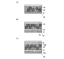
有機化合物層中の光触媒物質の混入状態の例として図2及び図3に光触媒物質を含む有機化合物層において、有機化合物層中膜厚方向に光触媒物質の濃度勾配がある場合を示す。 As an example of the mixed state of the photocatalytic substance in the organic compound layer, FIG. 2 and FIG. 3 show a case where there is a concentration gradient of the photocatalytic substance in the organic compound layer thickness direction in the organic compound layer containing the photocatalytic substance.
図2(A)に示す光触媒物質を含む有機化合物層は本発明の光触媒物質を含む有機化合物層の一例であり、第1の基板70上に、光触媒物質混入領域85を有する有機化合物層86が形成され、有機化合物層86上に素子層73が形成されている。有機化合物層86内において混入する光触媒物質は濃度勾配を有しており、光触媒物質は有機化合物層86内に不均一に存在している。光触媒物質混入領域85は、有機化合物層86と素子層73との界面付近に有している。よって有機化合物層86中の光触媒物質の濃度は、有機化合物層86と素子層73との界面が、有機化合物層86中において最も高い。光触媒物質混入領域85は非光触媒物質混入領域と明確な界面を有さずに、有機化合物層内で膜厚方向に素子層73に近づくにつれ徐々に濃度が変化する構造とすることができる。
The organic compound layer containing the photocatalytic substance shown in FIG. 2A is an example of the organic compound layer containing the photocatalytic substance of the present invention, and the
光触媒物質に第1の基板70より光を照射し、その活性化したエネルギーによって有機化合物を分解し、強度の低下した光触媒物質を含む有機化合物層88を形成する。その後、素子層73上に第2の基板78を接着し、素子層73を第1の基板70より剥離する(図2(B乃至D)参照。)。光触媒物質による有機化合物層の粗化は、光触媒物質混入領域87で起こるため、層内部で素子層側の光触媒物質を含む有機化合物層89bと、基板側の光触媒物質を含む有機化合物層89aとで分離(分断)する。
The photocatalytic material is irradiated with light from the
図3(A)に示す光触媒物質を含む有機化合物層は本発明の光触媒物質を含む有機化合物層の一例であり、第1の基板70上に、光触媒物質混入領域80を有する有機化合物層81が形成され、有機化合物層81上に素子層73が形成されている。有機化合物層81内において混入する光触媒物質は濃度勾配を有しており、光触媒物質は有機化合物層81内に不均一に存在している。光触媒物質混入領域80は、有機化合物層81と第1の基板70との界面付近に有している。よって有機化合物層81中の光触媒物質の濃度は、有機化合物層81と第1の基板70との界面付近が、有機化合物層81中において最も高い。光触媒物質混入領域は非光触媒物質混入領域と明確な界面を有さずに、有機化合物層内で膜厚方向に素子層73に近づくにつれ徐々に濃度が変化する構造とすることができる。
The organic compound layer containing the photocatalytic substance shown in FIG. 3A is an example of the organic compound layer containing the photocatalytic substance of the present invention, and an
光触媒物質に第1の基板70より光を照射し、その活性化したエネルギーによって有機化合物を分解し、強度の低下した光触媒物質を含む有機化合物層83を形成する。その後、素子層73上に第2の基板78を接着し、素子層73を第1の基板70より剥離する(図3(B乃至D)参照。)。光触媒物質による有機化合物層の粗化は、光触媒物質混入領域82で起こるため、層内部で素子層側の光触媒物質を含む有機化合物層84bと、基板側の光触媒物質を含む有機化合物層84aとで分離(分断)する。
The photocatalytic substance is irradiated with light from the
また、光触媒物質を含む有機化合物層と素子層の間に絶縁層を設けてもよい。図4においては、光触媒物質を含む有機化合物層72と素子層73との間に絶縁層90が設けられている。絶縁層90は素子層への不純物等の汚染を防いだり、露光で用いられる光を吸収、または反射する材料を用いれば、素子層への光照射を遮蔽することもできる。また素子層を第1の基板70から剥離した後、絶縁層90は、そのまま素子層73を支持し封止する基板としても用いることができる。
An insulating layer may be provided between the organic compound layer containing the photocatalytic substance and the element layer. In FIG. 4, an insulating
本発明に用いることのできる光触媒物質としては、酸化チタン(TiO2)、チタン酸ストロンチウム(SrTiO3)、セレン化カドミウム(CdSe)、タンタル酸カリウム(KTaO3)、硫化カドミウム(CdS)、酸化ジルコニウム(ZrO2)、酸化ニオブ(Nb2O5)、酸化亜鉛(ZnO)、酸化鉄(Fe2O3)、酸化タングステン(WO3)等が好ましい。これら光触媒物質に紫外光領域の光(波長400nm以下、好ましくは380nm以下)を照射し、光触媒活性を生じさせることができる。 Photocatalytic substances that can be used in the present invention include titanium oxide (TiO 2 ), strontium titanate (SrTiO 3 ), cadmium selenide (CdSe), potassium tantalate (KTaO 3 ), cadmium sulfide (CdS), zirconium oxide. (ZrO 2 ), niobium oxide (Nb 2 O 5 ), zinc oxide (ZnO), iron oxide (Fe 2 O 3 ), tungsten oxide (WO 3 ) and the like are preferable. These photocatalytic substances can be irradiated with light in the ultraviolet region (wavelength 400 nm or less, preferably 380 nm or less) to cause photocatalytic activity.
複数の金属を含む酸化物半導体からなる光触媒物質の場合、構成元素の塩を混合、融解して形成することができる。溶媒を除去する必要があるときは、焼成、乾燥を行えばよい。具体的には、所定の温度(例えば、300℃以上)で加熱すればよく、好ましくは酸素を有する雰囲気で行う。 In the case of a photocatalytic substance made of an oxide semiconductor containing a plurality of metals, it can be formed by mixing and melting constituent element salts. When it is necessary to remove the solvent, baking and drying may be performed. Specifically, heating may be performed at a predetermined temperature (for example, 300 ° C. or higher), and preferably performed in an atmosphere containing oxygen.
この加熱処理により、光触媒物質は所定の結晶構造を有することができる。例えば、酸化チタン(TiO2)では、アナターゼ型やルチル−アナターゼ混合型を有し、低温相ではアナターゼ型が優先的に形成される。そのため光触媒物質が所定の結晶構造を有していない場合も加熱すればよい。 By this heat treatment, the photocatalytic substance can have a predetermined crystal structure. For example, titanium oxide (TiO 2 ) has an anatase type and a rutile-anatase mixed type, and the anatase type is preferentially formed in the low temperature phase. Therefore, heating may be performed even when the photocatalytic substance does not have a predetermined crystal structure.
更に光触媒物質へ遷移金属(Pd、Pt、Cr、Ni、V、Mn、Fe、Ce、Mo、W等)をドーピングすることにより、光触媒活性を向上させたり、可視光領域(波長400nm〜800nm)の光により光触媒活性を起こすことができる。遷移金属は、広いバンドギャップを持つ活性な光触媒の禁制帯内に新しい準位を形成し、可視光領域まで光の吸収範囲を拡大しうるからである。例えば、CrやNiのアクセプター型、VやMnのドナー型、Fe等の両性型、その他Ce、Mo、W等をドーピングすることができる。このように光の波長は光触媒物質によって決定することができるため、光照射とは光触媒物質を光触媒活性化させる波長の光を照射することを指す。 Furthermore, the photocatalytic substance can be doped with transition metals (Pd, Pt, Cr, Ni, V, Mn, Fe, Ce, Mo, W, etc.) to improve the photocatalytic activity or visible light region (wavelength 400 nm to 800 nm). Photocatalytic activity can be caused by the light. This is because transition metals can form a new level in the forbidden band of an active photocatalyst having a wide band gap, and can extend the light absorption range to the visible light region. For example, an acceptor type such as Cr or Ni, a donor type such as V or Mn, an amphoteric type such as Fe, and Ce, Mo, W, or the like can be doped. Thus, since the wavelength of light can be determined by the photocatalytic substance, the light irradiation means irradiation with light having a wavelength that activates the photocatalytic substance.
また光触媒物質を真空中又は水素環流中で加熱し還元させると、結晶中に酸素欠陥が発生する。このように遷移元素をドーピングしなくても、酸素欠陥は電子ドナーと同等の役割を果たす。特に、ゾルゲル法により形成する場合、酸素欠陥が最初から存在するため、還元しなくともよい。またN2等のガスをドープすることにより、酸素欠陥を形成することができる。 Further, when the photocatalytic substance is heated and reduced in vacuum or hydrogen reflux, oxygen defects are generated in the crystal. Thus, oxygen defects play the same role as electron donors even without doping with a transition element. In particular, in the case of forming by the sol-gel method, oxygen defects are present from the beginning, so that reduction is not necessary. Further, oxygen defects can be formed by doping a gas such as N 2 .
本発明に用いることのできる有機化合物としては、有機材料や、有機材料及び無機材料の混合材料を用いることができる。有機材料としては、シアノエチルセルロース系樹脂、ポリエチレン、ポリプロピレン、ポリスチレン系樹脂、シリコーン樹脂、エポキシ樹脂、フッ化ビニリデンなどの樹脂を用いることができる。また、芳香族ポリアミド、ポリベンゾイミダゾール(polybenzimidazole)などの耐熱性高分子、又はシロキサン樹脂を用いてもよい。なお、シロキサン樹脂とは、Si−O−Si結合を含む樹脂に相当する。シロキサンは、シリコン(Si)と酸素(O)との結合で骨格構造が構成される。置換基として、少なくとも水素を含む有機基(例えばアルキル基、アリール基)が用いられる。置換基として、フルオロ基を用いてもよい。または置換基として、少なくとも水素を含む有機基と、フルオロ基とを用いてもよい。また、ポリビニルアルコール、ポリビニルブチラールなどのビニル樹脂、フェノール樹脂、ノボラック樹脂、アクリル樹脂、メラミン樹脂、ウレタン樹脂、オキサゾール樹脂(ポリベンゾオキサゾール)等の樹脂材料を用いてもよい。 As an organic compound that can be used in the present invention, an organic material or a mixed material of an organic material and an inorganic material can be used. As the organic material, a resin such as cyanoethyl cellulose resin, polyethylene, polypropylene, polystyrene resin, silicone resin, epoxy resin, or vinylidene fluoride can be used. Alternatively, a heat-resistant polymer such as aromatic polyamide, polybenzimidazole, or siloxane resin may be used. Note that a siloxane resin corresponds to a resin including a Si—O—Si bond. Siloxane has a skeleton structure formed of a bond of silicon (Si) and oxygen (O). As a substituent, an organic group containing at least hydrogen (for example, an alkyl group or an aryl group) is used. A fluoro group may be used as a substituent. Alternatively, an organic group containing at least hydrogen and a fluoro group may be used as a substituent. Moreover, resin materials such as vinyl resins such as polyvinyl alcohol and polyvinyl butyral, phenol resins, novolac resins, acrylic resins, melamine resins, urethane resins, and oxazole resins (polybenzoxazole) may be used.
有機化合物に含まれる無機材料としては、酸化珪素、窒化珪素、酸化窒化珪素、窒化酸化珪素、窒化アルミニウム(AlN)、酸化窒化アルミニウム(AlON)、窒化酸化アルミニウム(AlNO)または酸化アルミニウム、酸化チタン(TiO2)、BaTiO3、SrTiO3、PbTiO3、KNbO3、PbNbO3、Ta2O3、BaTa2O6、LiTaO3、Y2O3、ZrO2、ZnS、その他の無機材料を含む物質から選ばれた材料を用いることができる。 Examples of the inorganic material included in the organic compound include silicon oxide, silicon nitride, silicon oxynitride, silicon nitride oxide, aluminum nitride (AlN), aluminum oxynitride (AlON), aluminum nitride oxide (AlNO), aluminum oxide, and titanium oxide ( TiO 2 ), BaTiO 3 , SrTiO 3 , PbTiO 3 , KNbO 3 , PbNbO 3 , Ta 2 O 3 , BaTa 2 O 6 , LiTaO 3 , Y 2 O 3 , ZrO 2 , ZnS, and other inorganic materials Selected materials can be used.
本発明に用いることのできる有機化合物を含む溶液の溶媒としては、有機化合物材料が溶解し、有機化合物層を形成する方法(各種ウエットプロセス)及び所望の膜厚に適した粘度の溶液を作製できるような溶媒を適宜選択すればよい。有機溶媒等を用いることができ、例えば有機化合物としてシロキサン樹脂を用いる場合は、プロピレングリコールモノメチルエーテル、プロピレングリコールモノメチルエーテルアセテート(PGMEAともいう)、3−メトシキ−3メチル−1−ブタノール(MMBともいう)などを用いることができる。 As a solvent of a solution containing an organic compound that can be used in the present invention, a method of dissolving an organic compound material to form an organic compound layer (various wet processes) and a solution having a viscosity suitable for a desired film thickness can be prepared. Such a solvent may be appropriately selected. For example, when a siloxane resin is used as the organic compound, propylene glycol monomethyl ether, propylene glycol monomethyl ether acetate (also referred to as PGMEA), 3-methoxy-3-methyl-1-butanol (also referred to as MMB). ) Etc. can be used.
本発明により、剥離前の形状及び特性を保った良好な状態で転置工程を行えるような、剥離工程を用いて半導体装置及び表示装置を作製できる。よって、より高信頼性の半導体装置を装置や工程を複雑化することなく、歩留まりよく作製できる。 According to the present invention, a semiconductor device and a display device can be manufactured by using a peeling process so that the transfer process can be performed in a good state while maintaining the shape and characteristics before peeling. Therefore, a highly reliable semiconductor device can be manufactured with high yield without complicating the device and the process.
(実施の形態2)
本実施の形態では、本発明の転置工程を適用する表示装置の一構成例に関して図面を用いて説明する。より具体的には、表示装置の構成がパッシブマトリクス型の場合に関して示す。
(Embodiment 2)
In this embodiment, a structural example of a display device to which the transposition process of the present invention is applied will be described with reference to the drawings. More specifically, the case where the structure of the display device is a passive matrix type will be described.
表示装置は、第1の方向に延びた第1の電極層751a、第1の電極層751b、第1の電極層751c、第1の電極層751a、第1の電極層751b、第1の電極層751cを覆って設けられた電界発光層752と、第1の方向と垂直な第2の方向に延びた第2の電極層753a、第2の電極層753b、第2の電極層753cとを有している(図5(A)参照。)。第1の電極層751a、第1の電極層751b、第1の電極層751cと第2の電極層753a、第2の電極層753b、第2の電極層753aとの間に電界発光層752が設けられている。また、第2の電極層753a、第2の電極層753b、第2の電極層753aを覆うように、保護膜として機能する絶縁層754を設けており、第1の電極層751a、第1の電極層751b、第1の電極層751c、第2の電極層753a、第2の電極層753b、第2の電極層753a、電界発光層752及び絶縁層754が設けられた素子層は基板758に接して設けられている(図5(B)参照。)。なお、隣接する各々の発光素子間において横方向への電界の影響が懸念される場合は、各発光素子に設けられた電界発光層752を分離してもよい。
The display device includes a
図5(C)は、図5(B)の変形例であり、第1の電極層791a、第1の電極層791b、第1の電極層791c、電界発光層792、第2の電極層793b、保護層である絶縁層794が、基板798に接して設けられている。図5(C)の第1の電極層791a、第1の電極層791b、第1の電極層791cのように、第1の電極層は、テーパーを有する形状でもよく、曲率半径が連続的に変化する形状でもよい。第1の電極層791a、第1の電極層791b、第1の電極層791cのような形状は、液滴吐出法などを用いて形成することができる。このような曲率を有する曲面であると、積層する絶縁層や導電層のカバレッジがよい。
FIG. 5C is a modification example of FIG. 5B, and includes a
また、第1の電極層の端部を覆うように隔壁(絶縁層)を形成してもよい。隔壁(絶縁層)は、他の発光素子間を隔てる壁のような役目を果たす。図8(A)、(B)に第1の電極層の端部を隔壁(絶縁層)で覆う構造を示す。 In addition, a partition wall (insulating layer) may be formed so as to cover an end portion of the first electrode layer. The partition wall (insulating layer) serves as a wall separating other light emitting elements. 8A and 8B illustrate a structure in which the end portion of the first electrode layer is covered with a partition wall (insulating layer).
図8(A)に示す発光素子の一例は、隔壁(絶縁層)775が、第1の電極層771a、第1の電極層771b、第1の電極層771cの端部を覆うようにテーパーを有する形状で形成されている。第1の電極層771a、第1の電極層771b、第1の電極層771c上に、隔壁(絶縁層)775、電界発光層772、第2の電極層773b、絶縁層774、及び絶縁層776が設けられた素子層が、基板778に接して設けられている。
8A, the partition wall (insulating layer) 775 is tapered so as to cover end portions of the
図8(B)に示す発光素子の一例は、隔壁(絶縁層)765が曲率を有し、その曲率半径が連続的に変化する形状である。第1の電極層761a、第1の電極層761b、第1の電極層761c、電界発光層762、第2の電極層763b、絶縁層764が設けられた素子層が、基板768に接して設けられている。
An example of the light-emitting element illustrated in FIG. 8B has a shape in which the partition wall (insulating layer) 765 has a curvature, and the radius of curvature continuously changes. An element layer provided with the
本発明では光触媒物質を有機化合物層に分散させることによって、光触媒物質の光触媒機能を用いて有機化合物を分解(破壊)して層の有機化合物を粗にし、基板より素子層を剥離する。そのため、剥離のために素子層に大きな力をかける必要もないので、剥離工程で素子が破壊されることもなく、良好な形状で簡単に様々な基板に自由に転置を行うことができる。光触媒物質を含む有機化合物層の剥離後の素子層側の残存層が光触媒物質を含む有機化合物層759b、769b、779b、799bである。 In the present invention, by dispersing the photocatalytic substance in the organic compound layer, the organic compound is decomposed (destroyed) using the photocatalytic function of the photocatalytic substance to roughen the organic compound in the layer, and the element layer is peeled from the substrate. Therefore, since it is not necessary to apply a large force to the element layer for peeling, the element is not destroyed in the peeling process, and can be freely transferred to various substrates with a good shape. The remaining layers on the element layer side after peeling of the organic compound layer containing the photocatalytic substance are organic compound layers 759b, 769b, 779b, and 799b containing the photocatalytic substance.
よって、自由に様々な基板に転置することができるため、基板の材料の選択性の幅が広がる。また安価な材料を基板として選択することもでき、用途に合わせて広い機能を持たせることができるだけでなく、低コストで半導体装置を作製することができる。 Therefore, since it can be freely transferred to various substrates, the range of substrate material selectivity is widened. In addition, an inexpensive material can be selected as the substrate, so that not only a wide function can be provided depending on the application, but also a semiconductor device can be manufactured at low cost.
図6に図5(A)及び(B)の表示装置の作製工程を示す。図6(A)において、第1の基板750と第1の電極層751a、751b、751cとの間に光触媒物質を含む有機化合物層756が設けられている。第1の基板750は素子層に含まれる表示素子を形成する工程での処理(加熱処理など)に耐えうる、作成工程条件に適した基板を選択すればよい。光触媒物質を含む有機化合物層756中には光触媒物質が含まれている。
FIG. 6 illustrates a manufacturing process of the display device in FIGS. In FIG. 6A, an
その後、透光性を有する第1の基板750側より、光源780から、第1の基板750を通過させて光781を光触媒物質へ照射する(図6(B)参照。)。
After that, light 781 is irradiated from the
光触媒物質は、光781を吸収し活性化する。その活性エネルギーは、光触媒物質を含む有機化合物層756中に含まれる周囲の有機化合物に作用し、結果として有機化合物の物性を変化させ、改質する。つまり、活性化した光触媒物質のエネルギー(酸化力)により、有機化合物の炭素−水素結合、炭素−炭素結合が分離され、有機化合物の一部が二酸化炭素及び水となり脱ガス化する。結果、光触媒物質を含む有機化合物層756が粗になり、光触媒物質を含む有機化合物層757となる。光触媒物質を含む有機化合物層が粗になるとは、層の有機化合物領域が粗化し、密度が低下することをいう。
The photocatalytic substance absorbs light 781 and activates it. The active energy acts on the surrounding organic compound contained in the
発光素子785を含む素子層の絶縁層754上に第2の基板758を設ける(図6(C)参照。)。第2の基板758は接着層などを用いて素子層と接着してもよいし、樹脂層のような保護層を素子層上に直接形成してもよい。
A
第2の基板758側に発光素子785を含む素子層を転置するために力を加えると、光触媒物質を含む有機化合物層757は、強度が低下しもろくなっているので、層内部で素子層側の光触媒物質を含む有機化合物層759bと、基板側の光触媒物質を含む有機化合物層759aとで分離(分断)する。従って、第1の基板750より発光素子785を含む素子層を剥離することができる。
When a force is applied to transfer the element layer including the light-emitting
図7は、本発明を適用したパッシブマトリクス型の液晶表示装置の作製工程を示す。図7において、光触媒物質を含む有機化合物層1707が形成され、第1の画素電極層1701a、1701b、1701c、配向膜として機能する絶縁層1712が設けられた第1の基板1700と、配向膜として機能する絶縁層1704、対向電極層1705、カラーフィルタとして機能する着色層1706が設けられた第2の基板1710とが液晶層1703を挟持して対向している。第1の基板1700と第1の画素電極層1701a、1701b、1701cとの間に光触媒物質を含む有機化合物層1707が設けられている。第1の基板1700は素子層に含まれる液晶表示素子1713を形成する工程での処理(加熱処理など)に耐えうる、作成工程条件に適した基板を選択すればよい。光触媒物質を含む有機化合物層1707中には光触媒物質が含まれている。
FIG. 7 shows a manufacturing process of a passive matrix liquid crystal display device to which the present invention is applied. In FIG. 7, an
その後、透光性を有する第1の基板1700側より、光源780から、第1の基板1700を通過させて光781を光触媒物質へ照射する(図6(B)参照。)。
After that, light 781 is irradiated from the
光触媒物質は、光781を吸収し活性化する。その活性エネルギーは、光触媒物質を含む有機化合物層1707中に含まれる周囲の有機化合物に作用し、結果として有機化合物の物性を変化させ、改質する。つまり、活性化した光触媒物質のエネルギー(酸化力)により、有機化合物の炭素−水素結合、炭素−炭素結合が分離され、有機化合物の一部が二酸化炭素及び水となり脱ガス化する。結果、光触媒物質を含む有機化合物層1707が粗になり、光触媒物質を含む有機化合物層1708となる。
The photocatalytic substance absorbs light 781 and activates it. The active energy acts on the surrounding organic compound contained in the
第2の基板1710側に液晶表示素子1713を含む素子層を転置するために力を加えると、光触媒物質を含む有機化合物層1708は、強度が低下しもろくなっているので、層内部で素子層側の光触媒物質を含む有機化合物層1709bと、基板側の光触媒物質を含む有機化合物層1709aとで分離(分断)する。従って、第1の基板1700より液晶表示素子1713を含む素子層を剥離することができる。
When a force is applied to displace the element layer including the liquid
第1の基板1700より液晶表示素子1713を含む素子層を剥離後、素子層の光触媒物質を含む有機化合物層1709a側に第3の基板1711を接着する(図7(D参照。)。接着する第3の基板1711は、素子層に残存している光触媒物質が活性化する波長の光を透過させないような材料とすればよい。
After the element layer including the liquid
本発明では光触媒物質を有機化合物層に分散させることによって、光触媒物質の光触媒機能を用いて有機化合物を分解(破壊)して層の有機化合物を粗にし、基板より素子層を剥離する。そのため、剥離のために素子層に大きな力をかける必要もないので、剥離工程で素子が破壊されることもなく、良好な形状で簡単に様々な基板に自由に転置を行うことができる。 In the present invention, by dispersing the photocatalytic substance in the organic compound layer, the organic compound is decomposed (destroyed) using the photocatalytic function of the photocatalytic substance to roughen the organic compound in the layer, and the element layer is peeled from the substrate. Therefore, since it is not necessary to apply a large force to the element layer for peeling, the element is not destroyed in the peeling process, and can be freely transferred to various substrates with a good shape.
よって、自由に様々な基板に転置することができるため、基板の材料の選択性の幅が広がる。また安価な材料を基板として選択することもでき、用途に合わせて広い機能を持たせることができるだけでなく、低コストで半導体装置を作製することができる。 Therefore, since it can be freely transferred to various substrates, the range of substrate material selectivity is widened. In addition, an inexpensive material can be selected as the substrate, so that not only a wide function can be provided depending on the application, but also a semiconductor device can be manufactured at low cost.
基板758、基板766、基板768、基板778、基板798としては、ガラス基板や可撓性基板の他、石英基板等を用いることができる。可撓性基板とは、折り曲げることができる(フレキシブル)基板のことであり、例えば、ポリカーボネート、ポリアリレート、ポリエーテルスルフォン等からなるプラスチック基板等が挙げられる。また、フィルム(ポリプロピレン、ポリエステル、ビニル、ポリフッ化ビニル、塩化ビニルなどからなる)、繊維質な材料からなる紙、基材フィルム(ポリエステル、ポリアミド、無機蒸着フィルム、紙類等)などを用いることもできる。
As the
本実施の形態で示した第1の電極層、第2の電極層、電界発光層の材料および形成方法は、上記実施の形態1で示した材料および形成方法のいずれかを用いて同様に行うことができる。
The materials and formation methods of the first electrode layer, the second electrode layer, and the electroluminescent layer described in this embodiment are similarly performed using any of the materials and formation methods described in
隔壁(絶縁層)765、隔壁(絶縁層)775としては、酸化珪素、窒化珪素、酸化窒化珪素、酸化アルミニウム、窒化アルミニウム、酸窒化アルミニウムその他の無機絶縁性材料、又はアクリル酸、メタクリル酸及びこれらの誘導体、又はポリイミド(polyimide)、芳香族ポリアミド、ポリベンゾイミダゾール(polybenzimidazole)などの耐熱性高分子、又はシロキサン樹脂を用いてもよい。また、ポリビニルアルコール、ポリビニルブチラールなどのビニル樹脂、エポキシ樹脂、フェノール樹脂、ノボラック樹脂、アクリル樹脂、メラミン樹脂、ウレタン樹脂等の樹脂材料を用いる。また、ベンゾシクロブテン、パリレン、フッ化アリレンエーテル、ポリイミドなどの有機材料、水溶性ホモポリマーと水溶性共重合体を含む組成物材料等を用いてもよい。作製法としては、プラズマCVD法や熱CVD法などの気相成長法やスパッタリング法を用いることができる。また、液滴吐出法や、印刷法(スクリーン印刷やオフセット印刷などパターンが形成される方法)を用いることもできる。塗布法で得られる膜やSOG膜なども用いることができる。 As the partition wall (insulating layer) 765 and the partition wall (insulating layer) 775, silicon oxide, silicon nitride, silicon oxynitride, aluminum oxide, aluminum nitride, aluminum oxynitride, and other inorganic insulating materials, acrylic acid, methacrylic acid, and the like Or a heat resistant polymer such as polyimide, aromatic polyamide, polybenzimidazole, or a siloxane resin. Further, a resin material such as a vinyl resin such as polyvinyl alcohol or polyvinyl butyral, an epoxy resin, a phenol resin, a novolac resin, an acrylic resin, a melamine resin, or a urethane resin is used. Further, an organic material such as benzocyclobutene, parylene, fluorinated arylene ether, polyimide, a composition material containing a water-soluble homopolymer and a water-soluble copolymer, or the like may be used. As a manufacturing method, a vapor deposition method such as a plasma CVD method or a thermal CVD method, or a sputtering method can be used. Alternatively, a droplet discharge method or a printing method (a method for forming a pattern such as screen printing or offset printing) can be used. A film obtained by a coating method, an SOG film, or the like can also be used.
また、液滴吐出法により、導電層、絶縁層などを、組成物を吐出し形成した後、その平坦性を高めるために表面を圧力によってプレスして平坦化してもよい。プレスの方法としては、ローラー状のものを表面に走査することによって凹凸を軽減する、また平坦な板状な物で表面をプレスするなどを行ってもよい。プレスする時に、加熱工程を行っても良い。また溶剤等によって表面を軟化、または融解させエアナイフで表面の凹凸部を除去しても良い。また、CMP法を用いて研磨しても良い。この工程は、液滴吐出法によって凹凸が生じる場合に、その表面の平坦化する場合適用することができる。 Further, after a conductive layer, an insulating layer, or the like is formed by discharging a composition by a droplet discharge method, the surface may be flattened by pressing with a pressure in order to improve the flatness. As a pressing method, unevenness may be reduced by scanning a roller-shaped object on the surface, or the surface may be pressed with a flat plate-like object. A heating step may be performed when pressing. Alternatively, the surface may be softened or melted with a solvent or the like, and the surface irregularities may be removed with an air knife. Further, polishing may be performed using a CMP method. This step can be applied when the surface is flattened when unevenness is generated by the droplet discharge method.
本発明により、剥離前の形状及び特性を保った良好な状態で転置工程を行えるような、剥離工程を用いて半導体装置及び表示装置を作製できる。よって、より高信頼性の半導体装置を装置や工程を複雑化することなく、歩留まりよく作製できる。 According to the present invention, a semiconductor device and a display device can be manufactured by using a peeling process so that the transfer process can be performed in a good state while maintaining the shape and characteristics before peeling. Therefore, a highly reliable semiconductor device can be manufactured with high yield without complicating the device and the process.
(実施の形態3)
本実施の形態では本発明の転置工程を用いて作製したトランジスタを有する半導体装置について説明する。
(Embodiment 3)
In this embodiment, a semiconductor device including a transistor manufactured using the transposition process of the present invention will be described.
図9において、透光性を有する基板500上に設けられた透光性を有する絶縁層512と、トランジスタ510a及び510bを含む素子層との間に光触媒物質を含む有機化合物層516が設けられている。第1の基板500及び絶縁層512は素子層に含まれる表示素子を形成する工程での処理(加熱処理など)に耐えうる、作成工程条件に適した材料を選択すればよい。光触媒物質を含む有機化合物層516中には光触媒物質が含まれている。
In FIG. 9, an
その後、透光性を有する第1の基板500側より、光源580から、第1の基板500及び絶縁層512を通過させて光581を光触媒物質へ照射する(図9(B)参照。)。
After that, the photocatalytic substance is irradiated with light 581 from the
光触媒物質は、光581を吸収し活性化する。その活性エネルギーは、光触媒物質を含む有機化合物層516中に含まれる周囲の有機化合物に作用し、結果として有機化合物の物性を変化させ、改質する。つまり、活性化した光触媒物質のエネルギー(酸化力)により、有機化合物の炭素−水素結合、炭素−炭素結合が分離され、有機化合物の一部が二酸化炭素及び水となり脱ガス化する。結果、光触媒物質を含む有機化合物層516が粗になり、光触媒物質を含む有機化合物層517となる。
The photocatalytic substance absorbs light 581 and activates it. The active energy acts on the surrounding organic compound contained in the
トランジスタ510a及び510bを含む素子層の絶縁膜509、絶縁層511上に第2の基板518を設ける(図9(C)参照。)。第2の基板518は接着層などを用いて素子層と接着してもよいし、樹脂層のような保護層を素子層上に直接形成してもよい。
A
第2の基板518側にトランジスタ510a及び510bを含む素子層を転置するために力を加えると、光触媒物質を含む有機化合物層517は、強度が低下しもろくなっているので、層内部で素子層側の光触媒物質を含む有機化合物層519bと、基板側の光触媒物質を含む有機化合物層519aとで分離(分断)する。従って、第1の基板500よりトランジスタ510a及び510bを含む素子層を剥離することができる。
When force is applied to transfer the element layer including the
本実施の形態における図9では、トランジスタ510a及び510bはチャネルエッチ型逆スタガトランジスタの例を示す。図9において、トランジスタ510a及び510bは、ゲート電極層502a、502b、ゲート絶縁層508、半導体層504a、504b、一導電型を有する半導体層503a、503b、503c、503d、ソース電極層又はドレイン電極層である配線層505a、505b、505c、505dを含む。
In FIG. 9 in this embodiment mode, the
半導体層を形成する材料は、シランやゲルマンに代表される半導体材料ガスを用いて気相成長法やスパッタリング法で作製される非晶質半導体(以下「アモルファス半導体:AS」ともいう。)、該非晶質半導体を光エネルギーや熱エネルギーを利用して結晶化させた多結晶半導体、或いはセミアモルファス(微結晶若しくはマイクロクリスタルとも呼ばれる。以下「SAS」ともいう。)半導体などを用いることができる。 As a material for forming the semiconductor layer, an amorphous semiconductor (hereinafter also referred to as “amorphous semiconductor: AS”) manufactured by a vapor deposition method or a sputtering method using a semiconductor material gas typified by silane or germane is used. A polycrystalline semiconductor obtained by crystallizing a crystalline semiconductor using light energy or thermal energy, or a semi-amorphous (also referred to as microcrystal or microcrystal; hereinafter, also referred to as “SAS”) semiconductor can be used.
SASは、非晶質と結晶構造(単結晶、多結晶を含む)の中間的な構造を有し、自由エネルギー的に安定な第3の状態を有する半導体であって、短距離秩序を持ち格子歪みを有する結晶質な領域を含んでいる。SASは、珪素を含む気体をグロー放電分解(プラズマCVD)して形成する。珪素を含む気体としては、SiH4、その他にもSi2H6、SiH2Cl2、SiHCl3、SiCl4、SiF4などを用いることが可能である。またF2、GeF4を混合させても良い。この珪素を含む気体をH2、又は、H2とHe、Ar、Kr、Neから選ばれた一種または複数種の希ガス元素で希釈しても良い。また、ヘリウム、アルゴン、クリプトン、ネオンなどの希ガス元素を含ませて格子歪みをさらに助長させることで安定性が増し良好なSASが得られる。また半導体膜としてフッ素系ガスより形成されるSAS層に水素系ガスより形成されるSAS層を積層してもよい。 SAS is a semiconductor having an intermediate structure between amorphous and crystalline structures (including single crystal and polycrystal) and having a third state that is stable in terms of free energy and has a short-range order and a lattice. It includes a crystalline region with strain. SAS is formed by glow discharge decomposition (plasma CVD) of a gas containing silicon. As a gas containing silicon, SiH 4 , Si 2 H 6 , SiH 2 Cl 2 , SiHCl 3 , SiCl 4 , SiF 4, or the like can be used. Further, F 2 and GeF 4 may be mixed. The gas containing silicon may be diluted with H 2 , or H 2 and one or more kinds of rare gas elements selected from He, Ar, Kr, and Ne. Further, by adding a rare gas element such as helium, argon, krypton, or neon to further promote lattice distortion, stability is improved and a favorable SAS can be obtained. In addition, a SAS layer formed of a hydrogen-based gas may be stacked on a SAS layer formed of a fluorine-based gas as a semiconductor film.
非晶質半導体としては、代表的には水素化アモルファスシリコン、結晶性半導体としては代表的にはポリシリコンなどがあげられる。ポリシリコン(多結晶シリコン)には、800℃以上のプロセス温度を経て形成されるポリシリコンを主材料として用いた所謂高温ポリシリコンや、600℃以下のプロセス温度で形成されるポリシリコンを主材料として用いた所謂低温ポリシリコン、また結晶化を促進する元素などを添加し結晶化させたポリシリコンなどを含んでいる。もちろん、前述したように、セミアモルファス半導体又は半導体膜の一部に結晶相を含む半導体を用いることもできる。 A typical example of an amorphous semiconductor is hydrogenated amorphous silicon, and a typical example of a crystalline semiconductor is polysilicon. Polysilicon (polycrystalline silicon) is mainly made of so-called high-temperature polysilicon using polysilicon formed through a process temperature of 800 ° C. or more as a main material, or polysilicon formed at a process temperature of 600 ° C. or less. And so-called low-temperature polysilicon, and polysilicon crystallized by adding an element that promotes crystallization. Needless to say, as described above, a semi-amorphous semiconductor or a semiconductor containing a crystal phase in part of a semiconductor film can also be used.
半導体膜に、結晶性半導体膜を用いる場合、その結晶性半導体膜の作製方法は、公知の方法(レーザ結晶化法、熱結晶化法、またはニッケルなどの結晶化を助長する元素を用いた熱結晶化法等)を用いれば良い。また、SASである微結晶半導体をレーザ照射して結晶化し、結晶性を高めることもできる。結晶化を助長する元素を導入しない場合は、非晶質半導体膜にレーザ光を照射する前に、窒素雰囲気下500℃で1時間加熱することによって非晶質半導体膜の含有水素濃度を1×10²⁰atoms/cm3以下にまで放出させる。これは水素を多く含んだ非晶質半導体膜にレーザ光を照射すると非晶質半導体膜が破壊されてしまうからである。結晶化のための加熱処理は、加熱炉、レーザ照射、若しくはランプから発する光の照射(ランプアニールともいう)などを用いることができる。加熱方法としてGRTA(Gas Rapid Thermal Anneal)法、LRTA(Lamp Rapid Thermal Anneal)法等のRTA法がある。GRTAとは高温のガスを用いて加熱処理を行う方法であり、LRTAとはランプ光により加熱処理を行う方法である。 In the case where a crystalline semiconductor film is used as the semiconductor film, a method for manufacturing the crystalline semiconductor film can be a known method (laser crystallization method, thermal crystallization method, or heat using an element that promotes crystallization such as nickel. A crystallization method or the like may be used. In addition, a microcrystalline semiconductor that is a SAS can be crystallized by laser irradiation to improve crystallinity. In the case where an element for promoting crystallization is not introduced, the concentration of hydrogen contained in the amorphous semiconductor film is set to 1 × by heating at 500 ° C. for 1 hour in a nitrogen atmosphere before irradiating the amorphous semiconductor film with laser light. Release to 10 20 atoms / cm 3 or less. This is because when an amorphous semiconductor film containing a large amount of hydrogen is irradiated with laser light, the amorphous semiconductor film is destroyed. As the heat treatment for crystallization, a heating furnace, laser irradiation, irradiation with light emitted from a lamp (also referred to as lamp annealing), or the like can be used. There are RTA methods such as a GRTA (Gas Rapid Thermal Anneal) method and an LRTA (Lamp Rapid Thermal Anneal) method as heating methods. GRTA is a method for performing heat treatment using a high-temperature gas, and LRTA is a method for performing heat treatment with lamp light.
また、非晶質半導体層を結晶化し、結晶性半導体層を形成する結晶化工程で、非晶質半導体層に結晶化を促進する元素(触媒元素、金属元素とも示す)を添加し、熱処理(550℃〜750℃で3分〜24時間)により結晶化を行ってもよい。結晶化を助長する元素としては、鉄(Fe)、ニッケル(Ni)、コバルト(Co)、ルテニウム(Ru)、ロジウム(Rh)、パラジウム(Pd)、オスニウム(Os)、イリジウム(Ir)、白金(Pt)、銅(Cu)及び金(Au)から選ばれた一種又は複数種類を用いることができる。 Further, in the crystallization step of crystallizing the amorphous semiconductor layer to form the crystalline semiconductor layer, an element for promoting crystallization (also referred to as a catalyst element or a metal element) is added to the amorphous semiconductor layer, and heat treatment ( Crystallization may be carried out at 550 ° C. to 750 ° C. for 3 minutes to 24 hours. Elements that promote crystallization include iron (Fe), nickel (Ni), cobalt (Co), ruthenium (Ru), rhodium (Rh), palladium (Pd), osmium (Os), iridium (Ir), and platinum. One or more types selected from (Pt), copper (Cu), and gold (Au) can be used.
非晶質半導体膜への金属元素の導入の仕方としては、当該金属元素を非晶質半導体膜の表面又はその内部に存在させ得る手法であれば特に限定はなく、例えばスパッタ法、CVD法、プラズマ処理法(プラズマCVD法も含む)、吸着法、金属塩の溶液を塗布する方法を使用することができる。このうち溶液を用いる方法は簡便であり、金属元素の濃度調整が容易であるという点で有用である。また、このとき非晶質半導体膜の表面のぬれ性を改善し、非晶質半導体膜の表面全体に水溶液を行き渡らせるため、酸素雰囲気中でのUV光の照射、熱酸化法、ヒドロキシラジカルを含むオゾン水又は過酸化水素による処理等により、酸化膜を成膜することが望ましい。 The method of introducing the metal element into the amorphous semiconductor film is not particularly limited as long as the metal element can be present on the surface of the amorphous semiconductor film or inside the amorphous semiconductor film. For example, sputtering, CVD, A plasma treatment method (including a plasma CVD method), an adsorption method, or a method of applying a metal salt solution can be used. Among these, the method using a solution is simple and useful in that the concentration of the metal element can be easily adjusted. At this time, in order to improve the wettability of the surface of the amorphous semiconductor film and to spread the aqueous solution over the entire surface of the amorphous semiconductor film, irradiation with UV light in an oxygen atmosphere, thermal oxidation method, hydroxy radical It is desirable to form an oxide film by treatment with ozone water or hydrogen peroxide.
結晶化を促進する元素を結晶性半導体層から除去、又は軽減するため、結晶性半導体層に接して、不純物元素を含む半導体層を形成し、ゲッタリングシンクとして機能させる。不純物元素としては、n型を付与する不純物元素、p型を付与する不純物元素や希ガス元素などを用いることができ、例えばリン(P)、窒素(N)、ヒ素(As)、アンチモン(Sb)、ビスマス(Bi)、ボロン(B)、ヘリウム(He)、ネオン(Ne)、アルゴン(Ar)、Kr(クリプトン)、Xe(キセノン)から選ばれた一種または複数種を用いることができる。結晶化を促進する元素を含む結晶性半導体層に、希ガス元素を含む半導体層を形成し、熱処理(550℃〜750℃で3分〜24時間)を行う。結晶性半導体層中に含まれる結晶化を促進する元素は、希ガス元素を含む半導体層中に移動し、結晶性半導体層中の結晶化を促進する元素は除去、又は軽減される。その後、ゲッタリングシンクとなった希ガス元素を含む半導体層を除去する。 In order to remove or reduce an element that promotes crystallization from the crystalline semiconductor layer, a semiconductor layer containing an impurity element is formed in contact with the crystalline semiconductor layer and functions as a gettering sink. As the impurity element, an impurity element imparting n-type conductivity, an impurity element imparting p-type conductivity, a rare gas element, or the like can be used. For example, phosphorus (P), nitrogen (N), arsenic (As), antimony (Sb ), Bismuth (Bi), boron (B), helium (He), neon (Ne), argon (Ar), Kr (krypton), and Xe (xenon) can be used. A semiconductor layer containing a rare gas element is formed over the crystalline semiconductor layer containing an element that promotes crystallization, and heat treatment (at 550 ° C. to 750 ° C. for 3 minutes to 24 hours) is performed. The element that promotes crystallization contained in the crystalline semiconductor layer moves into the semiconductor layer containing a rare gas element, and the element that promotes crystallization in the crystalline semiconductor layer is removed or reduced. After that, the semiconductor layer containing a rare gas element that has become a gettering sink is removed.
レーザと、半導体膜とを相対的に走査することにより、レーザ照射を行うことができる。またレーザ照射において、ビームを精度よく重ね合わせたり、レーザ照射開始位置やレーザ照射終了位置を制御するため、マーカーを形成することもできる。マーカーは非晶質半導体膜と同時に、基板上へ形成すればよい。 Laser irradiation can be performed by relatively scanning the laser and the semiconductor film. In laser irradiation, a marker can be formed in order to superimpose beams with high accuracy and to control the laser irradiation start position and laser irradiation end position. The marker may be formed on the substrate simultaneously with the amorphous semiconductor film.
レーザ照射を用いる場合、連続発振型のレーザビーム(CW(CW:continuous−wave)レーザビーム)やパルス発振型のレーザビーム(パルスレーザビーム)を用いることができる。ここで用いることができるレーザビームは、Arレーザ、Krレーザ、エキシマレーザなどの気体レーザ、単結晶のYAG、YVO4、フォルステライト(Mg2SiO4)、YAlO3、GdVO4、若しくは多結晶(セラミック)のYAG、Y2O3、YVO4、YAlO3、GdVO4に、ドーパントとしてNd、Yb、Cr、Ti、Ho、Er、Tm、Taのうち1種または複数種添加されているものを媒質とするレーザ、ガラスレーザ、ルビーレーザ、アレキサンドライトレーザ、Ti:サファイアレーザ、銅蒸気レーザまたは金蒸気レーザのうち一種または複数種から発振されるものを用いることができる。このようなレーザビームの基本波、又はこれらの基本波の第2高調波から第4高調波のレーザビームを照射することで、大粒径の結晶を得ることができる。例えば、Nd:YVO4レーザ(基本波1064nm)の第2高調波(532nm)や第3高調波(355nm)を用いることができる。このレーザは、CWで射出することも、パルス発振で射出することも可能である。CWで射出する場合は、レーザのパワー密度は0.01〜100MW/cm2程度(好ましくは0.1〜10MW/cm2)が必要である。そして、走査速度を10〜2000cm/sec程度として照射する。 When laser irradiation is used, a continuous wave laser beam (CW (continuous-wave) laser beam) or a pulsed laser beam (pulse laser beam) can be used. The laser beam that can be used here is a gas laser such as an Ar laser, a Kr laser, or an excimer laser, single crystal YAG, YVO 4 , forsterite (Mg 2 SiO 4 ), YAlO 3 , GdVO 4 , or polycrystalline ( (Ceramics) YAG, Y 2 O 3 , YVO 4 , YAlO 3 , GdVO 4 with one or more of Nd, Yb, Cr, Ti, Ho, Er, Tm, Ta added as dopants A laser oscillated from one or more of laser, glass laser, ruby laser, alexandrite laser, Ti: sapphire laser, copper vapor laser, or gold vapor laser as a medium can be used. By irradiating the fundamental wave of such a laser beam, or the second to fourth harmonics of these fundamental waves, a crystal having a large grain size can be obtained. For example, a second harmonic (532 nm) or a third harmonic (355 nm) of an Nd: YVO 4 laser (fundamental wave 1064 nm) can be used. This laser can be emitted by CW or pulsed oscillation. When injected at a CW, the power density of the laser is about 0.01 to 100 MW / cm 2 (preferably 0.1 to 10 MW / cm 2) is required. Then, irradiation is performed at a scanning speed of about 10 to 2000 cm / sec.
なお、単結晶のYAG、YVO4、フォルステライト(Mg2SiO4)、YAlO3、GdVO4、若しくは多結晶(セラミック)のYAG、Y2O3、YVO4、YAlO3、GdVO4に、ドーパントとしてNd、Yb、Cr、Ti、Ho、Er、Tm、Taのうち1種または複数種添加されているものを媒質とするレーザ、Arイオンレーザ、またはTi:サファイアレーザは、連続発振をさせることが可能であり、Qスイッチ動作やモード同期などを行うことによって10MHz以上の発振周波数でパルス発振をさせることも可能である。10MHz以上の発振周波数でレーザビームを発振させると、半導体膜がレーザによって溶融してから固化するまでの間に、次のパルスが半導体膜に照射される。従って、発振周波数が低いパルスレーザを用いる場合と異なり、半導体膜中において固液界面を連続的に移動させることができるため、走査方向に向かって連続的に成長した結晶粒を得ることができる。 Note that single crystal YAG, YVO 4 , forsterite (Mg 2 SiO 4 ), YAlO 3 , GdVO 4 , or polycrystalline (ceramic) YAG, Y 2 O 3 , YVO 4 , YAlO 3 , GdVO 4 , dopants Nd, Yb, Cr, Ti, Ho, Er, Tm, Ta, a laser using a medium added with one or more, an Ar ion laser, or a Ti: sapphire laser should oscillate continuously It is also possible to perform pulse oscillation at an oscillation frequency of 10 MHz or more by performing Q switch operation, mode synchronization, or the like. When the laser beam is oscillated at an oscillation frequency of 10 MHz or more, the semiconductor film is irradiated with the next pulse during the period from when the semiconductor film is melted by the laser to solidification. Therefore, unlike the case of using a pulse laser having a low oscillation frequency, the solid-liquid interface can be continuously moved in the semiconductor film, so that crystal grains continuously grown in the scanning direction can be obtained.
媒質としてセラミック(多結晶)を用いると、短時間かつ低コストで自由な形状に媒質を形成することが可能である。単結晶を用いる場合、通常、直径数mm、長さ数十mmの円柱状の媒質が用いられているが、セラミックを用いる場合はさらに大きいものを作ることが可能である。 When ceramic (polycrystal) is used as the medium, it is possible to form the medium in a free shape in a short time and at low cost. When a single crystal is used, a cylindrical medium having a diameter of several millimeters and a length of several tens of millimeters is usually used. However, when ceramic is used, a larger one can be made.
発光に直接寄与する媒質中のNd、Ybなどのドーパントの濃度は、単結晶中でも多結晶中でも大きくは変えられないため、濃度を増加させることによるレーザの出力向上にはある程度限界がある。しかしながら、セラミックの場合、単結晶と比較して媒質の大きさを著しく大きくすることができるため大幅な出力向上ができる。 Since the concentration of dopants such as Nd and Yb in the medium that directly contributes to light emission cannot be changed greatly regardless of whether it is a single crystal or a polycrystal, there is a certain limit to improving the laser output by increasing the concentration. However, in the case of ceramic, since the size of the medium can be remarkably increased as compared with the single crystal, the output can be greatly improved.
さらに、セラミックの場合では、平行六面体形状や直方体形状の媒質を容易に形成することが可能である。このような形状の媒質を用いて、発振光を媒質の内部でジグザグに進行させると、発振光路を長くとることができる。そのため、増幅が大きくなり、大出力で発振させることが可能になる。また、このような形状の媒質から射出されるレーザビームは射出時の断面形状が四角形状であるため、丸状のビームと比較すると、線状ビームに整形するのに有利である。このように射出されたレーザビームを、光学系を用いて整形することによって、短辺の長さ1mm以下、長辺の長さ数mm〜数mの線状ビームを容易に得ることが可能となる。また、励起光を媒質に均一に照射することにより、線状ビームは長辺方向にエネルギー分布の均一なものとなる。またさらにレーザは、半導体膜に対して入射角θ(0<θ<90度)を持たせて照射させるとよい。レーザの干渉を防止することができるからである。 Further, in the case of ceramic, a medium having a parallelepiped shape or a rectangular parallelepiped shape can be easily formed. When a medium having such a shape is used to cause oscillation light to travel in a zigzag manner inside the medium, the oscillation optical path can be made longer. As a result, amplification is increased and oscillation can be performed with high output. Further, since the laser beam emitted from the medium having such a shape has a quadrangular cross-sectional shape at the time of emission, it is advantageous for shaping into a linear beam as compared with a round beam. By shaping the emitted laser beam using an optical system, it is possible to easily obtain a linear beam having a short side length of 1 mm or less and a long side length of several mm to several m. Become. In addition, by irradiating the medium with the excitation light uniformly, the linear beam has a uniform energy distribution in the long side direction. Further, the laser may be irradiated with an incident angle θ (0 <θ <90 degrees) with respect to the semiconductor film. This is because laser interference can be prevented.
この線状ビームを半導体膜に照射することによって、半導体膜の全面をより均一にアニールすることが可能になる。線状ビームの両端まで均一なアニールが必要な場合は、その両端にスリットを配置し、エネルギーの減衰部を遮光するなどの工夫が必要となる。 By irradiating the semiconductor film with this linear beam, the entire surface of the semiconductor film can be annealed more uniformly. When uniform annealing is required up to both ends of the linear beam, it is necessary to arrange a slit at both ends to shield the energy attenuating portion.
このようにして得られた強度が均一な線状ビームを用いて半導体膜をアニールし、この半導体膜を用いて表示装置を作製すると、その表示装置の特性は、良好かつ均一である。 When a semiconductor film is annealed using a linear beam with uniform intensity obtained in this way and a display device is manufactured using this semiconductor film, the characteristics of the display device are good and uniform.
また、希ガスや窒素などの不活性ガス雰囲気中でレーザ光を照射するようにしても良い。これにより、レーザ光の照射により半導体表面の荒れを抑えることができ、界面準位密度のばらつきによって生じるしきい値のばらつきを抑えることができる。 Further, laser light may be irradiated in an inert gas atmosphere such as a rare gas or nitrogen. Accordingly, the surface roughness of the semiconductor can be suppressed by laser light irradiation, and variations in threshold values caused by variations in interface state density can be suppressed.
非晶質半導体膜の結晶化は、熱処理とレーザ光照射による結晶化を組み合わせてもよく、熱処理やレーザ光照射を単独で、複数回行っても良い。 Crystallization of the amorphous semiconductor film may be a combination of heat treatment and crystallization by laser light irradiation, or may be performed multiple times by heat treatment or laser light irradiation alone.
ゲート電極層は、スパッタリング法、蒸着法、CVD法等の手法により形成することができる。ゲート電極層はタンタル(Ta)、タングステン(W)、チタン(Ti)、モリブデン(Mo)、アルミニウム(Al)、銅(Cu)、クロム(Cr)、ネオジウム(Nd)から選ばれた元素、又は前記元素を主成分とする合金材料もしくは化合物材料で形成すればよい。また、ゲート電極層としてリン等の不純物元素をドーピングした多結晶シリコン膜に代表される半導体膜や、AgPdCu合金を用いてもよい。また、ゲート電極層は単層でも積層でもよい。 The gate electrode layer can be formed by a technique such as sputtering, vapor deposition, or CVD. The gate electrode layer is an element selected from tantalum (Ta), tungsten (W), titanium (Ti), molybdenum (Mo), aluminum (Al), copper (Cu), chromium (Cr), neodymium (Nd), or What is necessary is just to form with the alloy material or compound material which has the said element as a main component. Alternatively, a semiconductor film typified by a polycrystalline silicon film doped with an impurity element such as phosphorus, or an AgPdCu alloy may be used for the gate electrode layer. The gate electrode layer may be a single layer or a stacked layer.
本実施の形態ではゲート電極層をテーパー形状を有する様に形成するが、本発明はそれに限定されず、ゲート電極層を積層構造にして、一層のみがテーパー形状を有し、他方は異方性エッチングによって垂直な側面を有していてもよい。テーパー角度も積層するゲート電極層間で異なっていても良いし、同一でもよい。テーパー形状を有することによって、その上に積層する膜の被覆性が向上し、欠陥が軽減されるので信頼性が向上する。 In this embodiment mode, the gate electrode layer is formed to have a tapered shape; however, the present invention is not limited thereto, and the gate electrode layer has a stacked structure, and only one layer has a tapered shape, and the other is anisotropic. You may have a vertical side surface by an etching. The taper angle may also be different between the stacked gate electrode layers, or may be the same. By having a tapered shape, the coverage of a film stacked thereon is improved and defects are reduced, so that reliability is improved.
ソース電極層又はドレイン電極層は、PVD法、CVD法、蒸着法等により導電膜を成膜した後、所望の形状にエッチングして形成することができる。また、液滴吐出法、印刷法、ディスペンサ法、電界メッキ法等により、所定の場所に選択的に導電層を形成することができる。更にはリフロー法、ダマシン法を用いても良い。ソース電極層又はドレイン電極層の材料は、Ag、Au、Cu、Ni、Pt、Pd、Ir、Rh、W、Al、Ta、Mo、Cd、Zn、Fe、Ti、Zr、Ba等の金属、Si、Ge、又はその合金、若しくはその窒化物を用いて形成する。また、これらの積層構造としても良い。 The source electrode layer or the drain electrode layer can be formed by forming a conductive film by a PVD method, a CVD method, an evaporation method, or the like and then etching the conductive film into a desired shape. In addition, a conductive layer can be selectively formed at a predetermined place by a droplet discharge method, a printing method, a dispenser method, an electroplating method, or the like. Furthermore, a reflow method or a damascene method may be used. The source electrode layer or drain electrode layer is made of Ag, Au, Cu, Ni, Pt, Pd, Ir, Rh, W, Al, Ta, Mo, Cd, Zn, Fe, Ti, Zr, Ba or other metals, It is formed using Si, Ge, an alloy thereof, or a nitride thereof. Moreover, it is good also as these laminated structures.
絶縁層512、511、509としては、酸化珪素、窒化珪素、酸化窒化珪素、酸化アルミニウム、窒化アルミニウム、酸窒化アルミニウムその他の無機絶縁性材料、又はアクリル酸、メタクリル酸及びこれらの誘導体、又はポリイミド(polyimide)、芳香族ポリアミド、ポリベンゾイミダゾール(polybenzimidazole)などの耐熱性高分子、又はシロキサン樹脂を用いてもよい。また、ポリビニルアルコール、ポリビニルブチラールなどのビニル樹脂、エポキシ樹脂、フェノール樹脂、ノボラック樹脂、アクリル樹脂、メラミン樹脂、ウレタン樹脂等の樹脂材料を用いる。また、ベンゾシクロブテン、パリレン、フッ化アリレンエーテル、ポリイミドなどの有機材料、水溶性ホモポリマーと水溶性共重合体を含む組成物材料等を用いてもよい。作製法としては、プラズマCVD法や熱CVD法などの気相成長法やスパッタリング法を用いることができる。また、液滴吐出法や、印刷法(スクリーン印刷やオフセット印刷などパターンが形成される方法)を用いることもできる。塗布法で得られる膜やSOG膜なども用いることができる。
As the insulating
また、液滴吐出法により、導電層、絶縁層などを、組成物を吐出し形成した後、その平坦性を高めるために表面を圧力によってプレスして平坦化してもよい。プレスの方法としては、ローラー状のものを表面に走査することによって凹凸を軽減する、また平坦な板状な物で表面をプレスするなどを行ってもよい。プレスする時に、加熱工程を行っても良い。また溶剤等によって表面を軟化、または融解させエアナイフで表面の凹凸部を除去しても良い。また、CMP法を用いて研磨しても良い。この工程は、液滴吐出法によって凹凸が生じる場合に、その表面の平坦化する場合適用することができる。 Further, after a conductive layer, an insulating layer, or the like is formed by discharging a composition by a droplet discharge method, the surface may be flattened by pressing with a pressure in order to improve the flatness. As a pressing method, unevenness may be reduced by scanning a roller-shaped object on the surface, or the surface may be pressed with a flat plate-like object. A heating step may be performed when pressing. Alternatively, the surface may be softened or melted with a solvent or the like, and the surface irregularities may be removed with an air knife. Further, polishing may be performed using a CMP method. This step can be applied when the surface is flattened when unevenness is generated by the droplet discharge method.
本実施の形態に限定されず、薄膜トランジスタはチャネル形成領域が一つ形成されるシングルゲート構造でも、二つ形成されるダブルゲート構造もしくは三つ形成されるトリプルゲート構造であっても良い。また、周辺駆動回路領域の薄膜トランジスタも、シングルゲート構造、ダブルゲート構造もしくはトリプルゲート構造であっても良い。 Without being limited to this embodiment mode, the thin film transistor may have a single gate structure in which one channel formation region is formed, a double gate structure in which two channel formation regions are formed, or a triple gate structure in which three channel formation regions are formed. The thin film transistor in the peripheral driver circuit region may have a single gate structure, a double gate structure, or a triple gate structure.
なお、本実施の形態で示した薄膜トランジスタの作製方法に限らず、トップゲート型(例えば順スタガ型、コプラナ型)、ボトムゲート型(例えば、逆コプラナ型)、あるいはチャネル領域の上下にゲート絶縁膜を介して配置された2つのゲート電極層を有する、デュアルゲート型やその他の構造においても適用できる。 Note that the gate insulating film is not limited to the method for manufacturing the thin film transistor described in this embodiment mode, and may be a top gate type (eg, a forward stagger type or a coplanar type), a bottom gate type (eg, a reverse coplanar type), or a gate insulating film above and below a channel region. The present invention can also be applied to a dual gate type or other structure having two gate electrode layers arranged via each other.
本実施の形態では、光触媒物質に対する光照射を行ってから可撓性を有する対向基板を貼り付ける例を示すが、転置する基板を素子層に貼り付けた後に光触媒物質に光を照射してもよい。 In this embodiment mode, an example in which a flexible counter substrate is attached after light irradiation to the photocatalyst material is described. However, even if the photocatalyst material is irradiated with light after the substrate to be transferred is attached to the element layer, Good.
本発明では光触媒物質を有機化合物層に分散させることによって、光触媒物質の光触媒機能を用いて有機化合物を分解(破壊)して層の有機化合物を粗にし、基板より素子層を剥離する。そのため、剥離のために素子層に大きな力をかける必要もないので、剥離工程で素子が破壊されることもなく、良好な形状で簡単に様々な基板に自由に転置を行うことができる。 In the present invention, by dispersing the photocatalytic substance in the organic compound layer, the organic compound is decomposed (destroyed) using the photocatalytic function of the photocatalytic substance to roughen the organic compound in the layer, and the element layer is peeled from the substrate. Therefore, since it is not necessary to apply a large force to the element layer for peeling, the element is not destroyed in the peeling process, and can be freely transferred to various substrates with a good shape.
よって、自由に様々な基板に転置することができるため、基板の材料の選択性の幅が広がる。また安価な材料を基板として選択することもでき、用途に合わせて広い機能を持たせることができるだけでなく、低コストで半導体装置を作製することができる。 Therefore, since it can be freely transferred to various substrates, the range of substrate material selectivity is widened. In addition, an inexpensive material can be selected as the substrate, so that not only a wide function can be provided depending on the application, but also a semiconductor device can be manufactured at low cost.
(実施の形態4)
本実施の形態では、上記実施の形態2とは異なる構成を有する表示装置について説明する。具体的には、表示装置の構成がアクティブマトリクス型の場合に関して示す。
(Embodiment 4)
In this embodiment mode, a display device having a structure different from that of
表示装置の上面図を図10(A)に、図10(A)における線E−Fの断面図を図10(B)に示す。また、図10(A)には、電界発光層532、第2の電極層533及び絶縁層534は省略され図示されていないが、図10(B)で示すようにそれぞれ設けられている。
10A is a top view of the display device, and FIG. 10B is a cross-sectional view taken along line EF in FIG. 10A. In FIG. 10A, the
第1の方向に延びた第1の配線と、第1の方向と垂直な第2の方向に延びた第2の配線とがマトリクス状に設けられている。また、第1の配線はトランジスタ521のソース電極又はドレイン電極に接続されており、第2の配線はトランジスタ521のゲート電極に接続されている。さらに、第1の配線と接続されていないトランジスタ521のソース電極またはドレイン電極に、第1の電極層531が接続され、第1の電極層531、電界発光層532、第2の電極層533の積層構造によって発光素子530が設けられている。隣接する各々の発光素子の間に隔壁(絶縁層)528を設けて、第1の電極層と隔壁(絶縁層)528上に電界発光層532および第2の電極層533を積層して設けている。第2の電極層533上に保護層となる絶縁層534を有している。また、トランジスタ521として、図9で示した逆スタガ型薄膜トランジスタを用いている(図10(B)及び図11(A)参照。)。
A first wiring extending in the first direction and a second wiring extending in a second direction perpendicular to the first direction are provided in a matrix. The first wiring is connected to the source electrode or the drain electrode of the
図10(B)の表示装置において、発光素子は第3の基板540に光触媒物質を含む有機化合物層539bを介して設けられており、絶縁層523、絶縁層526、絶縁層527、隔壁(絶縁層)528、トランジスタ521を有している。
10B, the light-emitting element is provided over the
図11に図10(A)及び(B)の表示装置の作製工程を示す。図11において、第1の基板520と、トランジスタ521及び発光素子530を含む素子層との間に光触媒物質を含む有機化合物層524が設けられている。第1の基板520は素子層に含まれる表示素子を形成する工程での処理(加熱処理など)に耐えうる、作成工程条件に適した基板を選択すればよい。光触媒物質を含む有機化合物層524中には光触媒物質が含まれている。
FIG. 11 illustrates a manufacturing process of the display device in FIGS. In FIG. 11, an
その後、透光性を有する第1の基板520側より、光源580から、第1の基板520を通過させて光581を光触媒物質へ照射する(図11(B)参照。)。
After that, the photocatalytic substance is irradiated with light 581 from the
光触媒物質は、光581を吸収し活性化する。その活性エネルギーは、光触媒物質を含む有機化合物層524中に含まれる周囲の有機化合物に作用し、結果として有機化合物の物性を変化させ、改質する。つまり、活性化した光触媒物質のエネルギー(酸化力)により、有機化合物の炭素−水素結合、炭素−炭素結合が分離され、有機化合物の一部が二酸化炭素及び水となり脱ガス化する。結果、光触媒物質を含む有機化合物層524が粗になり、光触媒物質を含む有機化合物層537となる。
The photocatalytic substance absorbs light 581 and activates it. The active energy acts on the surrounding organic compound contained in the
トランジスタ521及び発光素子530を含む素子層の絶縁層534上に第2の基板538を設ける(図11(C)参照。)。第2の基板538は接着層などを用いて素子層と接着してもよいし、樹脂層のような保護層を素子層上に直接形成してもよい。
A
第2の基板538側にトランジスタ521及び発光素子530を含む素子層を転置するために力を加えると、光触媒物質を含む有機化合物層537は、強度が低下しもろくなっているので、層内部で素子層側の光触媒物質を含む有機化合物層539bと、基板側の光触媒物質を含む有機化合物層539aとで分離(分断)する。従って、第1の基板520よりトランジスタ521及び発光素子530を含む素子層を剥離することができる。
When force is applied to transfer the element layer including the
図12は、本発明を適用したアクティブマトリクス型の液晶表示装置の作製工程を示す。図12において、光触媒物質を含む有機化合物層566が形成され、マルチゲート構造のトランジスタ551及び画素電極層560、配向膜として機能する絶縁層561が設けられた第1の基板550と、配向膜として機能する絶縁層563、対向電極層564、カラーフィルタとして機能する着色層565が設けられた第2の基板568とが液晶層562を挟持して対向している。第1の基板550とトランジスタ551及び画素電極層560を含む素子層との間に光触媒物質を含む有機化合物層566が設けられている。第1の基板550は素子層に含まれる液晶表示素子を形成する工程での処理(加熱処理など)に耐えうる、作成工程条件に適した基板を選択すればよい。光触媒物質を含む有機化合物層566中には光触媒物質が含まれている。
FIG. 12 shows a manufacturing process of an active matrix liquid crystal display device to which the present invention is applied. In FIG. 12, an
その後、透光性を有する第1の基板550側より、光源580から、第1の基板550を通過させて光581を光触媒物質へ照射する(図12(B)参照。)。
After that, the photocatalytic substance is irradiated with light 581 from the
光触媒物質は、光581を吸収し活性化する。その活性エネルギーは、光触媒物質を含む有機化合物層566中に含まれる周囲の有機化合物に作用し、結果として有機化合物の物性を変化させ、改質する。つまり、活性化した光触媒物質のエネルギー(酸化力)により、有機化合物の炭素−水素結合、炭素−炭素結合が分離され、有機化合物の一部が二酸化炭素及び水となり脱ガス化する。結果、光触媒物質を含む有機化合物層566が粗になり、光触媒物質を含む有機化合物層570となる。
The photocatalytic substance absorbs light 581 and activates it. The active energy acts on the surrounding organic compound contained in the
第2の基板568側にトランジスタ551及び液晶表示素子を含む素子層を転置するために力を加えると、光触媒物質を含む有機化合物層566は、強度が低下しもろくなっているので、層内部で素子層側の光触媒物質を含む有機化合物層569bと、基板側の光触媒物質を含む有機化合物層569aとで分離(分断)する。従って、第1の基板550よりトランジスタ551及び表示素子を含む素子層を剥離することができる(図12(C)参照。)。
When force is applied to transfer the element layer including the
本発明では光触媒物質を有機化合物層に分散させることによって、光触媒物質の光触媒機能を用いて有機化合物を分解(破壊)して層の有機化合物を粗にし、基板より素子層を剥離する。そのため、剥離のために素子層に大きな力をかける必要もないので、剥離工程で素子が破壊されることもなく、良好な形状で簡単に様々な基板に自由に転置を行うことができる。 In the present invention, by dispersing the photocatalytic substance in the organic compound layer, the organic compound is decomposed (destroyed) using the photocatalytic function of the photocatalytic substance to roughen the organic compound in the layer, and the element layer is peeled from the substrate. Therefore, since it is not necessary to apply a large force to the element layer for peeling, the element is not destroyed in the peeling process, and can be freely transferred to various substrates with a good shape.
よって、自由に様々な基板に転置することができるため、基板の材料の選択性の幅が広がる。また安価な材料を基板として選択することもでき、用途に合わせて広い機能を持たせることができるだけでなく、低コストで半導体装置を作製することができる。 Therefore, since it can be freely transferred to various substrates, the range of substrate material selectivity is widened. In addition, an inexpensive material can be selected as the substrate, so that not only a wide function can be provided depending on the application, but also a semiconductor device can be manufactured at low cost.
図13は、本発明を適用したアクティブマトリクス型の電子ペーパーの作製工程を示す。図13ではアクティブマトリクス型を示すが、本発明はパッシブマトリクス型にも適用することができる。 FIG. 13 shows a manufacturing process of an active matrix electronic paper to which the present invention is applied. Although FIG. 13 shows an active matrix type, the present invention can also be applied to a passive matrix type.
図12では、表示素子として液晶表示素子を用いて例を示したが、ツイストボール表示方式を用いた表示装置を用いてもよい。ツイストボール表示方式とは、白と黒に塗り分けられた球形粒子を第1の電極層及び第2の電極層の間に配置し、第1の電極層及び第2の電極層に電位差を生じさせての球形粒子の向きを制御することにより、表示を行う方法である。 Although FIG. 12 shows an example using a liquid crystal display element as a display element, a display device using a twisting ball display method may be used. In the twist ball display system, spherical particles that are separately painted in white and black are arranged between the first electrode layer and the second electrode layer, and a potential difference is generated between the first electrode layer and the second electrode layer. In this method, display is performed by controlling the orientation of the spherical particles.
透光性を有する基板596及び球形粒子589を含む素子層との間に光触媒物質を含む有機化合物層583が設けられている。第1の基板596は素子層に含まれる表示素子を形成する工程での処理(加熱処理など)に耐えうる、作成工程条件に適した基板を選択すればよい。光触媒物質を含む有機化合物層524中には光触媒物質が含まれている。
An
トランジスタ597は逆コプラナ型の薄膜トランジスタであり、ゲート電極層582、ゲート絶縁層584、配線層585a、配線層585b、半導体層586を含む。また配線層585bは第1の電極層587a、587bに、絶縁層598に形成する開口で接しており電気的に接続している。第1の電極層587a、587bと第2の電極層588との間には黒色領域590a及び白色領域590を有し、周りに液体で満たされているキャビティ594を含む球形粒子589が設けられており、球形粒子589の周囲は樹脂等の充填材595で充填されている(図13参照。)。
The transistor 597 is an inverted coplanar thin film transistor and includes a
その後、透光性を有する第1の基板596側より、光源580から、第1の基板596を通過させて光581を光触媒物質へ照射する(図13(B)参照。)。
After that, the light catalytic converter material is irradiated with light 581 from the
光触媒物質は、光581を吸収し活性化する。その活性エネルギーは、光触媒物質を含む有機化合物層583中に含まれる周囲の有機化合物に作用し、結果として有機化合物の物性を変化させ、改質する。つまり、活性化した光触媒物質のエネルギー(酸化力)により、有機化合物の炭素−水素結合、炭素−炭素結合が分離され、有機化合物の一部が二酸化炭素及び水となり脱ガス化する。結果、光触媒物質を含む有機化合物層583が粗になり、光触媒物質を含む有機化合物層591となる。
The photocatalytic substance absorbs light 581 and activates it. The active energy acts on the surrounding organic compound contained in the
第2の基板592側にトランジスタ597及び表示素子を含む素子層を転置するために力を加えると、光触媒物質を含む有機化合物層591は、強度が低下しもろくなっているので、層内部で素子層側の光触媒物質を含む有機化合物層593bと、基板側の光触媒物質を含む有機化合物層593aとで分離(分断)する。従って、第1の基板596よりトランジスタ597及び球形粒子589を含む素子層を剥離することができる(図13(C)参照。)。
When force is applied to transfer the element layer including the transistor 597 and the display element to the
本発明では光触媒物質を有機化合物層に分散させることによって、光触媒物質の光触媒機能を用いて有機化合物を分解(破壊)して層の有機化合物を粗にし、基板より素子層を剥離する。そのため、剥離のために素子層に大きな力をかける必要もないので、剥離工程で素子が破壊されることもなく、良好な形状で簡単に様々な基板に自由に転置を行うことができる。 In the present invention, by dispersing the photocatalytic substance in the organic compound layer, the organic compound is decomposed (destroyed) using the photocatalytic function of the photocatalytic substance to roughen the organic compound in the layer, and the element layer is peeled from the substrate. Therefore, since it is not necessary to apply a large force to the element layer for peeling, the element is not destroyed in the peeling process, and can be freely transferred to various substrates with a good shape.
よって、自由に様々な基板に転置することができるため、基板の材料の選択性の幅が広がる。また安価な材料を基板として選択することもでき、用途に合わせて広い機能を持たせることができるだけでなく、低コストで半導体装置を作製することができる。 Therefore, since it can be freely transferred to various substrates, the range of substrate material selectivity is widened. In addition, an inexpensive material can be selected as the substrate, so that not only a wide function can be provided depending on the application, but also a semiconductor device can be manufactured at low cost.
また、ツイストボールの代わりに、電気泳動素子を用いることも可能である。透明な液体と、正に帯電した白い微粒子と負に帯電した黒い微粒子とを封入した直径10μm〜200μm程度のマイクロカプセルを用いる。第1の電極層と第2の電極層との間に設けられるマイクロカプセルは、第1の電極層と第2の電極層によって、電場が与えられると、白い微粒子と、黒い微粒子が逆の方向に移動し、白または黒を表示することができる。この原理を応用した表示素子が電気泳動表示素子であり、一般的に電子ペーパーとよばれている。電気泳動表示素子は、液晶表示素子に比べて反射率が高いため、補助ライトは不要であり、また消費電力が小さく、薄暗い場所でも表示部を認識することが可能である。また、表示部に電源が供給されない場合であっても、一度表示した像を保持することが可能であるため、電波発信源から表示機能付き半導体装置を遠ざけた場合であっても、表示された像を保存しておくことが可能となる。 Further, instead of the twisting ball, an electrophoretic element can be used. A microcapsule having a diameter of about 10 μm to 200 μm in which transparent liquid, positively charged white microparticles, and negatively charged black microparticles are enclosed is used. In the microcapsule provided between the first electrode layer and the second electrode layer, when an electric field is applied by the first electrode layer and the second electrode layer, the white particles and the black particles are in opposite directions. And can display white or black. A display element using this principle is an electrophoretic display element, and is generally called electronic paper. Since the electrophoretic display element has higher reflectance than the liquid crystal display element, an auxiliary light is unnecessary, power consumption is small, and the display portion can be recognized even in a dim place. In addition, even when power is not supplied to the display unit, it is possible to retain the image once displayed. Therefore, even when the semiconductor device with a display function is moved away from the radio wave source, it is displayed. The image can be stored.
トランジスタはスイッチング素子として機能し得るものであれば、どのような構成で設けてもよい。半導体層も非晶質半導体、結晶性半導体、多結晶半導体、微結晶半導体など様々な半導体を用いることができ、有機化合物を用いて有機トランジスタを形成してもよい。 The transistor may have any structure as long as it can function as a switching element. As the semiconductor layer, various semiconductors such as an amorphous semiconductor, a crystalline semiconductor, a polycrystalline semiconductor, and a microcrystalline semiconductor can be used, and an organic transistor may be formed using an organic compound.
本発明により、剥離前の形状及び特性を保った良好な状態で転置工程を行えるような、剥離工程を用いて半導体装置及び表示装置を作製できる。よって、より高信頼性の半導体装置を装置や工程を複雑化することなく、歩留まりよく作製できる。 According to the present invention, a semiconductor device and a display device can be manufactured by using a peeling process so that the transfer process can be performed in a good state while maintaining the shape and characteristics before peeling. Therefore, a highly reliable semiconductor device can be manufactured with high yield without complicating the device and the process.
(実施の形態5)
本発明の実施の形態を、図14を用いて説明する。本実施の形態は、表示装置において、薄膜トランジスタとしてチャネルエッチ型逆スタガ型薄膜トランジスタを用い、トランジスタ上に層間絶縁層を形成しない例を示す。よって、同一部分又は同様な機能を有する部分の繰り返しの説明は省略する。図14(A)は、本発明の転置工程を用いて作製された発光表示装置の上面図であり、図14(B)は図14(A)の断面図である。
(Embodiment 5)
An embodiment of the present invention will be described with reference to FIG. This embodiment shows an example in which a channel-etched inverted staggered thin film transistor is used as a thin film transistor and an interlayer insulating layer is not formed over the transistor in the display device. Therefore, repetitive description of the same portion or a portion having a similar function is omitted. 14A is a top view of a light-emitting display device manufactured using the transposition process of the present invention, and FIG. 14B is a cross-sectional view of FIG.
図14(A)(B)で示すように、画素部655、走査線駆動回路である駆動回路領域651a、走査線駆動回路である駆動回路領域651b、駆動回路領域653が、シール材612によって、基板600と封止基板610との間に封止され、基板600上にICドライバによって形成された信号線駆動回路である駆動回路領域652が設けられている。基板600上に、駆動回路領域653に、逆スタガ型薄膜トランジスタ601、逆スタガ型薄膜トランジスタ602、画素部655に逆スタガ型薄膜トランジスタ603、ゲート絶縁層605、絶縁膜606、絶縁層609、第1の電極層604と、電界発光層607と、第2の電極層608との積層である発光素子650、充填材611、封止基板610、封止領域にシール材612、端子電極層613、異方性導電層614、FPC615が設けられている。
As shown in FIGS. 14A and 14B, the
本発明では光触媒物質を有機化合物層に分散させることによって、光触媒物質の光触媒機能を用いて有機化合物を分解(破壊)して層の有機化合物を粗にし、基板より素子層を剥離する。そのため、剥離のために素子層に大きな力をかける必要もないので、剥離工程で素子が破壊されることもなく、良好な形状で簡単に様々な基板に自由に転置を行うことができる。光触媒物質を含む有機化合物層の剥離後の素子層側の残存層が光触媒物質を含む有機化合物層630である。光触媒物質を含む有機化合物層630は封止基板610に転写後、研磨等によって除去しても構わない。
In the present invention, by dispersing the photocatalytic substance in the organic compound layer, the organic compound is decomposed (destroyed) using the photocatalytic function of the photocatalytic substance to roughen the organic compound in the layer, and the element layer is peeled from the substrate. Therefore, since it is not necessary to apply a large force to the element layer for peeling, the element is not destroyed in the peeling process, and can be freely transferred to various substrates with a good shape. The remaining layer on the element layer side after peeling of the organic compound layer containing the photocatalytic substance is the
よって、自由に様々な基板に転置することができるため、基板の材料の選択性の幅が広がる。また安価な材料を基板として選択することもでき、用途に合わせて広い機能を持たせることができるだけでなく、低コストで半導体装置を作製することができる。 Therefore, since it can be freely transferred to various substrates, the range of substrate material selectivity is widened. In addition, an inexpensive material can be selected as the substrate, so that not only a wide function can be provided depending on the application, but also a semiconductor device can be manufactured at low cost.
本実施の形態で作製される逆スタガ型薄膜トランジスタ601、逆スタガ型薄膜トランジスタ602、逆スタガ型薄膜トランジスタ603のゲート電極層、ソース電極層、及びドレイン電極層は液滴吐出法によって形成されている。液滴吐出法は、液状の導電性材料を有する組成物を吐出し、乾燥や焼成によって固化し、導電層や電極層を形成する方法である。絶縁性材料を含む組成物を吐出し、乾燥や焼成によって固化すれば絶縁層も形成することができる。選択的に導電層や絶縁層などの表示装置の構成物を形成することができるので、工程が簡略化し、材料のロスが防げるので、低コストで生産性良く表示装置を作製することができる。
The gate electrode layer, the source electrode layer, and the drain electrode layer of the inverted staggered
液滴吐出法に用いる液滴吐出手段とは、組成物の吐出口を有するノズルや、1つ又は複数のノズルを具備したヘッド等の液滴を吐出する手段を有するものの総称とする。液滴吐出手段が具備するノズルの径は、0.02〜100μm(好適には30μm以下)に設定し、該ノズルから吐出される組成物の吐出量は0.001pl〜100pl(好適には0.1pl以上40pl以下、より好ましくは10pl以下)に設定する。吐出量は、ノズルの径の大きさに比例して増加する。また、被処理物とノズルの吐出口との距離は、所望の箇所に滴下するために、出来る限り近づけておくことが好ましく、好適には0.1〜3mm(好適には1mm以下)程度に設定する。 The droplet discharge means used in the droplet discharge method is a general term for a device having means for discharging droplets such as a nozzle having a composition discharge port and a head having one or a plurality of nozzles. The diameter of the nozzle provided in the droplet discharge means is set to 0.02 to 100 μm (preferably 30 μm or less), and the discharge amount of the composition discharged from the nozzle is 0.001 pl to 100 pl (preferably 0). .1pl or more and 40pl or less, more preferably 10pl or less). The discharge amount increases in proportion to the size of the nozzle diameter. In addition, the distance between the object to be processed and the nozzle outlet is preferably as close as possible in order to drop it at a desired location, preferably about 0.1 to 3 mm (preferably about 1 mm or less). Set.
液滴吐出法を用いて膜(絶縁膜、又は導電膜など)を形成する場合、粒子状に加工された膜材料を含む組成物を吐出し、焼成によって融合や融着接合させ固化することで膜を形成する。このように導電性材料を含む組成物を吐出し、焼成することによって形成された膜においては、スパッタ法などで形成した膜が、多くは柱状構造を示すのに対し、多くの粒界を有する多結晶状態を示すことが多い。 When forming a film (insulating film, conductive film, or the like) using a droplet discharge method, a composition containing a film material processed into particles is discharged, and is fused and fused and solidified by firing. A film is formed. In a film formed by discharging and baking a composition containing a conductive material in this manner, a film formed by a sputtering method or the like often has a columnar structure, but has many grain boundaries. Often exhibits a polycrystalline state.
吐出口から吐出する組成物は、導電性材料を溶媒に溶解又は分散させたものを用いる。導電性材料とは、Ag、Au、Cu、Ni、Pt、Pd、Ir、Rh、W、Al等の金属、Cd、Znの金属硫化物、Fe、Ti、Ge、Zr、Baなどの酸化物、ハロゲン化銀の微粒子又は分散性ナノ粒子に相当する。前記導電性材料はそれらの混合物であってもよい。これらの透明導電膜として、インジウム錫酸化物(ITO)、インジウム錫酸化物と酸化珪素を含むITSO、有機インジウム、有機スズ、酸化亜鉛、窒化チタン等を用いることができる。また、酸化亜鉛(ZnO)を含むインジウム亜鉛酸化物(IZO(indium zinc oxide))、酸化亜鉛(ZnO)、ZnOにガリウム(Ga)をドープしたもの、酸化スズ(SnO2)、酸化タングステンを含むインジウム酸化物、酸化タングステンを含むインジウム亜鉛酸化物、酸化チタンを含むインジウム酸化物、酸化チタンを含むインジウム錫酸化物なども用いてもよい。但し、吐出口から吐出する組成物は、比抵抗値を考慮して、金、銀、銅のいずれかの材料を溶媒に溶解又は分散させたものを用いることが好適であり、より好適には、低抵抗な銀、銅を用いるとよい。但し、銀、銅を用いる場合には、不純物対策のため、合わせてバリア膜を設けるとよい。バリア膜としては、窒化珪素膜やニッケルボロン(NiB)を用いるとことができる。 A composition in which a conductive material is dissolved or dispersed in a solvent is used as the composition discharged from the discharge port. Conductive materials include metals such as Ag, Au, Cu, Ni, Pt, Pd, Ir, Rh, W, and Al, metal sulfides of Cd and Zn, and oxides such as Fe, Ti, Ge, Zr, and Ba Correspond to silver halide fine particles or dispersible nanoparticles. The conductive material may be a mixture thereof. As these transparent conductive films, indium tin oxide (ITO), ITSO containing indium tin oxide and silicon oxide, organic indium, organic tin, zinc oxide, titanium nitride, or the like can be used. Further, indium zinc oxide (IZO) containing zinc oxide (ZnO), zinc oxide (ZnO), ZnO doped with gallium (Ga), tin oxide (SnO 2 ), tungsten oxide is included. Indium oxide, indium zinc oxide containing tungsten oxide, indium oxide containing titanium oxide, indium tin oxide containing titanium oxide, or the like may also be used. However, it is preferable to use a composition in which any of gold, silver and copper is dissolved or dispersed in a solvent in consideration of the specific resistance value, more preferably the composition discharged from the discharge port. It is preferable to use low resistance silver or copper. However, when silver or copper is used, a barrier film may be provided as a countermeasure against impurities. As the barrier film, a silicon nitride film or nickel boron (NiB) can be used.
吐出する組成物は、導電性材料を溶媒に溶解又は分散させたものであるが、他にも分散剤や、熱硬化性樹脂が含まれている。特に熱硬化性樹脂に関しては、焼成時にクラックや不均一な焼きムラが発生するのを防止する働きを持つ。よって、形成される導電層には、有機材料が含まれることがある。含まれる有機材料は、加熱温度、雰囲気、時間により異なる。この有機材料は、金属粒子の熱硬化性樹脂、溶媒、分散剤、及び被覆剤として機能する有機樹脂などであり、代表的には、ポリイミド、アクリル、ノボラック樹脂、メラミン樹脂、フェノール樹脂、エポキシ樹脂、シリコーン樹脂、フラン樹脂、ジアリルフタレート樹脂等や、他の有機樹脂が挙げられる。 The composition to be discharged is one obtained by dissolving or dispersing a conductive material in a solvent, but additionally contains a dispersant and a thermosetting resin. In particular, the thermosetting resin has a function of preventing generation of cracks and uneven baking during firing. Thus, the formed conductive layer may contain an organic material. The organic material contained varies depending on the heating temperature, atmosphere, and time. This organic material is a thermosetting resin of metal particles, a solvent, a dispersant, an organic resin that functions as a coating agent, etc., and typically, polyimide, acrylic, novolac resin, melamine resin, phenol resin, epoxy resin , Silicone resin, furan resin, diallyl phthalate resin, and other organic resins.
また、導電性材料の周りに他の導電性材料がコーティングされ、複数の層になっている粒子でも良い。例えば、銅の周りにニッケルボロン(NiB)がコーティングされ、その周囲に銀がコーティングされている3層構造の粒子などを用いても良い。溶媒は、酢酸ブチル、酢酸エチル等のエステル類、イソプロピルアルコール、エチルアルコール等のアルコール類、メチルエチルケトン、アセトン等の有機溶剤等、又は水を用いる。組成物の粘度は20mPa・s(cp)以下が好適であり、これは、乾燥が起こることの防止や、吐出口からの組成物の円滑な吐出ができるようにするためである。また、組成物の表面張力は、40mN/m以下が好適である。但し、用いる溶媒や、用途に合わせて、組成物の粘度等は適宜調整するとよい。一例として、ITOや、有機インジウム、有機スズを溶媒に溶解又は分散させた組成物の粘度は5〜20mPa・s、銀を溶媒に溶解又は分散させた組成物の粘度は5〜20mPa・s、金を溶媒に溶解又は分散させた組成物の粘度は5〜20mPa・sに設定するとよい。 Alternatively, particles in which a conductive material is coated with another conductive material to form a plurality of layers may be used. For example, particles having a three-layer structure in which nickel boron (NiB) is coated around copper and silver is coated around it may be used. As the solvent, esters such as butyl acetate and ethyl acetate, alcohols such as isopropyl alcohol and ethyl alcohol, organic solvents such as methyl ethyl ketone and acetone, and water are used. The viscosity of the composition is preferably 20 mPa · s (cp) or less, in order to prevent the drying from occurring and to smoothly discharge the composition from the discharge port. The surface tension of the composition is preferably 40 mN / m or less. However, the viscosity and the like of the composition may be appropriately adjusted according to the solvent to be used and the application. As an example, the viscosity of a composition in which ITO, organic indium, or organic tin is dissolved or dispersed in a solvent is 5 to 20 mPa · s, the viscosity of a composition in which silver is dissolved or dispersed in a solvent is 5 to 20 mPa · s, The viscosity of the composition in which gold is dissolved or dispersed in a solvent is preferably set to 5 to 20 mPa · s.
また、導電層は、複数の導電性材料を積層しても良い。また、始めに導電性材料として銀を用いて、液滴吐出法で導電層を形成した後、銅などでめっきを行ってもよい。めっきは電気めっきや化学(無電界)めっき法で行えばよい。めっきは、めっきの材料を有する溶液を満たした容器に基板表面を浸してもよいが、基板を斜め(または垂直)に立てて設置し、めっきする材料を有する溶液を、基板表面に流すように塗布してもよい。基板を立てて溶液を塗布するようにめっきを行うと、工程装置が小型化する利点がある。 The conductive layer may be a stack of a plurality of conductive materials. Alternatively, first, silver may be used as a conductive material, and a conductive layer may be formed by a droplet discharge method, followed by plating with copper or the like. Plating may be performed by electroplating or chemical (electroless) plating. For plating, the substrate surface may be immersed in a container filled with a solution having a plating material, but the substrate is placed at an angle (or vertically) so that the solution having the material to be plated flows on the substrate surface. It may be applied. When plating is performed so that the solution is applied while standing the substrate, there is an advantage that the process apparatus is reduced in size.
各ノズルの径や所望のパターン形状などに依存するが、ノズルの目詰まり防止や高精細なパターンの作製のため、導電体の粒子の径はなるべく小さい方が好ましく、好適には粒径0.1μm以下の粒子サイズが好ましい。組成物は、電解法、アトマイズ法又は湿式還元法等の公知の方法で形成されるものであり、その粒子サイズは、一般的に約0.01〜10μmである。但し、ガス中蒸発法で形成すると、分散剤で保護されたナノ粒子は約7nmと微細であり、またこのナノ粒子は、被覆剤を用いて各粒子の表面を覆うと、溶剤中に凝集がなく、室温で安定に分散し、液体とほぼ同じ挙動を示す。従って、被覆剤を用いることが好ましい。 Although depending on the diameter of each nozzle and the desired pattern shape, the diameter of the conductor particles is preferably as small as possible for preventing nozzle clogging and producing a high-definition pattern. A particle size of 1 μm or less is preferred. The composition is formed by a known method such as an electrolytic method, an atomizing method, or a wet reduction method, and its particle size is generally about 0.01 to 10 μm. However, when formed by a gas evaporation method, the nanoparticles protected by the dispersant are as fine as about 7 nm, and these nanoparticles are aggregated in the solvent when the surface of each particle is covered with a coating agent. And stably disperse at room temperature and shows almost the same behavior as liquid. Therefore, it is preferable to use a coating agent.
また、組成物を吐出する工程は、減圧下で行ってもよい。減圧下で行うと、導電体の表面に酸化膜などが形成されないため好ましい。組成物を吐出後、乾燥と焼成の一方又は両方の工程を行う。乾燥と焼成の工程は、両工程とも加熱処理の工程であるが、例えば、乾燥は100度で3分間、焼成は200〜350度で15分間〜60分間で行うもので、その目的、温度と時間が異なるものである。乾燥の工程、焼成の工程は、常圧下又は減圧下で、レーザ光の照射や瞬間熱アニール、加熱炉などにより行う。なお、この加熱処理を行うタイミングは特に限定されない。乾燥と焼成の工程を良好に行うためには、基板を加熱しておいてもよく、そのときの温度は、基板等の材質に依存するが、一般的には100〜800度(好ましくは200〜350度)とする。本工程により、組成物中の溶媒の揮発、又は化学的に分散剤を除去するとともに、周囲の樹脂が硬化収縮することで、ナノ粒子間を接触させ、融合と融着を加速する。 The step of discharging the composition may be performed under reduced pressure. It is preferable to perform under reduced pressure because an oxide film or the like is not formed on the surface of the conductor. After discharging the composition, one or both steps of drying and baking are performed. The drying and firing steps are both heat treatment steps. For example, drying is performed at 100 degrees for 3 minutes, and firing is performed at 200 to 350 degrees for 15 minutes to 60 minutes. Time is different. The drying process and the firing process are performed under normal pressure or reduced pressure by laser light irradiation, rapid thermal annealing, a heating furnace, or the like. In addition, the timing which performs this heat processing is not specifically limited. In order to satisfactorily perform the drying and firing steps, the substrate may be heated, and the temperature at that time depends on the material of the substrate or the like, but is generally 100 to 800 degrees (preferably 200). ~ 350 degrees). By this step, the solvent in the composition is volatilized or the dispersant is chemically removed, and the surrounding resin is cured and contracted to bring the nanoparticles into contact with each other, thereby accelerating fusion and fusion.
レーザ光の照射は、連続発振またはパルス発振の気体レーザ又は固体レーザを用いれば良い。前者の気体レーザとしては、エキシマレーザ、YAGレーザ等が挙げられ、後者の固体レーザとしては、Cr、Nd等がドーピングされたYAG、YVO4、GdVO4等の結晶を使ったレーザ等が挙げられる。なお、レーザ光の吸収率の関係から、連続発振のレーザを用いることが好ましい。また、パルス発振と連続発振を組み合わせたレーザ照射方法を用いてもよい。但し、基板100の耐熱性に依っては、レーザ光の照射による加熱処理は、該基板100を破壊しないように、数マイクロ秒から数十秒の間で瞬間的に行うとよい。瞬間熱アニール(RTA)は、不活性ガスの雰囲気下で、紫外光乃至赤外光を照射する赤外ランプやハロゲンランプなどを用いて、急激に温度を上昇させ、数分〜数マイクロ秒の間で瞬間的に熱を加えて行う。この処理は瞬間的に行うために、最表面の薄膜のみを加熱することができ、下層の膜には影響を与えない。つまり、プラスチック基板等の耐熱性が弱い基板にも影響を与えない。 For the laser light irradiation, a continuous wave or pulsed gas laser or solid-state laser may be used. Examples of the former gas laser include an excimer laser and a YAG laser, and examples of the latter solid-state laser include a laser using a crystal such as YAG, YVO 4 , and GdVO 4 doped with Cr, Nd, or the like. . Note that it is preferable to use a continuous wave laser because of the absorption rate of the laser light. Further, a laser irradiation method combining pulse oscillation and continuous oscillation may be used. However, depending on the heat resistance of the substrate 100, the heat treatment by laser light irradiation may be performed instantaneously within a few microseconds to several tens of seconds so as not to destroy the substrate 100. Instantaneous thermal annealing (RTA) uses an infrared lamp or a halogen lamp that irradiates ultraviolet light or infrared light in an inert gas atmosphere, and rapidly raises the temperature for several minutes to several microseconds. This is done by applying heat instantaneously. Since this process is performed instantaneously, only the outermost thin film can be heated, and the underlying film is not affected. That is, it does not affect a substrate having low heat resistance such as a plastic substrate.
また、液滴吐出法により、導電層、絶縁層を、液状の組成物を吐出し形成した後、その平坦性を高めるために表面を圧力によってプレスして平坦化してもよい。プレスの方法としては、ローラー状のものを表面に走査することによって凹凸を軽減する、また平坦な板状な物で表面をプレスするなどを行ってもよい。プレスする時に、加熱工程を行っても良い。また溶剤等によって表面を軟化、または融解させエアナイフで表面の凹凸部を除去しても良い。また、CMP法を用いて研磨しても良い。この工程は、液滴吐出法によって凹凸が生じる場合に、その表面の平坦化する場合適用することができる。 Further, after the conductive layer and the insulating layer are formed by discharging a liquid composition by a droplet discharge method, the surface may be flattened by pressing with a pressure in order to improve the flatness. As a pressing method, unevenness may be reduced by scanning a roller-shaped object on the surface, or the surface may be pressed with a flat plate-like object. A heating step may be performed when pressing. Alternatively, the surface may be softened or melted with a solvent or the like, and the surface irregularities may be removed with an air knife. Further, polishing may be performed using a CMP method. This step can be applied when the surface is flattened when unevenness is generated by the droplet discharge method.
本実施の形態では、半導体層として非晶質半導体を用いており、一導電性型を有する半導体層は必要に応じて形成すればよい。本実施の形態では、半導体層と一導電型を有する半導体層として非晶質N型半導体層を積層する。またN型半導体層を形成し、nチャネル型TFTのNMOS構造、p型半導体層を形成したpチャネル型TFTのPMOS構造、nチャネル型TFTとpチャネル型TFTとのCMOS構造を作製することができる。本実施の形態では、逆スタガ型薄膜トランジスタ601と逆スタガ型薄膜トランジスタ603をnチャネル型TFT、逆スタガ型薄膜トランジスタ602をpチャネル型TFTで形成しており、駆動回路領域653において、逆スタガ型薄膜トランジスタ601と逆スタガ型薄膜トランジスタ602はCMOS構造となっている。
In this embodiment mode, an amorphous semiconductor is used as a semiconductor layer, and a semiconductor layer having one conductivity type may be formed as needed. In this embodiment mode, an amorphous N-type semiconductor layer is stacked as a semiconductor layer and a semiconductor layer having one conductivity type. In addition, an N-type semiconductor layer is formed, and an NMOS structure of an n-channel TFT, a PMOS structure of a p-channel TFT having a p-type semiconductor layer, and a CMOS structure of an n-channel TFT and a p-channel TFT are manufactured. it can. In this embodiment mode, the inverted staggered
また、導電性を付与するために、導電性を付与する元素をドーピングによって添加し、不純物領域を半導体層に形成することで、nチャネル型TFT、pチャネル型TFTを形成することもできる。N型半導体層を形成するかわりに、PH3ガスによるプラズマ処理を行うことによって、半導体層に導電性を付与してもよい。 Further, in order to impart conductivity, an n-channel TFT or a p-channel TFT can be formed by adding an element imparting conductivity by doping and forming an impurity region in the semiconductor layer. Instead of forming the N-type semiconductor layer, conductivity may be imparted to the semiconductor layer by performing plasma treatment with a PH 3 gas.
また、半導体として、有機半導体材料を用い、印刷法、スプレー法、スピン塗布法、液滴吐出法、ディスペンサ法などで形成することができる。この場合、上記エッチング工程が必要ないため、工程数を削減することが可能である。有機半導体としては、ペンタセンなどの低分子材料、高分子材料などが用いられ、有機色素、導電性高分子材料などの材料も用いることができる。本発明に用いる有機半導体材料としては、その骨格が共役二重結合から構成されるπ電子共役系の高分子材料が望ましい。代表的には、ポリチオフェン、ポリフルオレン、ポリ(3−アルキルチオフェン)、ポリチオフェン誘導体等の可溶性の高分子材料を用いることができる。 Alternatively, an organic semiconductor material can be used as a semiconductor and can be formed by a printing method, a spray method, a spin coating method, a droplet discharge method, a dispenser method, or the like. In this case, the number of processes can be reduced because the etching process is not necessary. As the organic semiconductor, a low molecular material such as pentacene, a polymer material, or the like is used, and materials such as an organic dye or a conductive polymer material can also be used. The organic semiconductor material used in the present invention is preferably a π-electron conjugated polymer material whose skeleton is composed of conjugated double bonds. Typically, a soluble polymer material such as polythiophene, polyfluorene, poly (3-alkylthiophene), or a polythiophene derivative can be used.
本発明により、剥離前の形状及び特性を保った良好な状態で転置工程を行えるような、剥離工程を用いて半導体装置及び表示装置を作製できる。よって、より高信頼性の半導体装置を装置や工程を複雑化することなく、歩留まりよく作製できる。 According to the present invention, a semiconductor device and a display device can be manufactured by using a peeling process so that the transfer process can be performed in a good state while maintaining the shape and characteristics before peeling. Therefore, a highly reliable semiconductor device can be manufactured with high yield without complicating the device and the process.
(実施の形態6)
本発明の実施の形態を、図15を用いて説明する。図15は本発明の剥離工程を用いて作製する液晶表示装置である。
(Embodiment 6)
An embodiment of the present invention will be described with reference to FIG. FIG. 15 shows a liquid crystal display device manufactured using the peeling process of the present invention.
図15(A)は、本発明の転置工程を用いて作製された液晶表示装置の上面図であり、図15(B)は図15(A)の断面図である。 15A is a top view of a liquid crystal display device manufactured using the transposition process of the present invention, and FIG. 15B is a cross-sectional view of FIG.
図15(A)で示すように、画素部256、走査線駆動回路である駆動回路領域258a、走査線駆動回路である駆動回路領域258bが、シール材282によって、基板200と対向基板210との間に封止され、基板200上にICドライバによって形成された信号線駆動回路である駆動回路領域257が設けられている。画素部256にはトランジスタ220が設けられている。基板200は、剥離された素子層及び光触媒物質を含む有機化合物層230と接着しており、素子層に残存している光触媒物質が活性化する波長の光を透過させないような材料とすればよい。また、対向基板210、基板200は可撓性を有する基板、また樹脂膜などを用いる。また一般的に合成樹脂からなる基板は、他の基板と比較して耐熱温度が低いことが懸念されるが、耐熱性の高い基板を用いた作製工程の後、転置することによっても採用することが可能となる。
As shown in FIG. 15A, a
図15に示す表示装置は、基板200上に、画素部に逆スタガ型薄膜トランジスタであるトランジスタ220、画素電極層201、絶縁層202、配向膜として機能する絶縁層203、液晶層204、スペーサ281、配向膜として機能する絶縁層205、対向電極層206、カラーフィルタとして機能する着色層208、ブラックマトリクス207、対向基板210、偏光板231、封止領域にシール材282、端子電極層287、異方性導電層285、FPC286が設けられている。
15 includes a
本実施の形態で作製される逆スタガ型薄膜トランジスタであるトランジスタ220のゲート電極層、ソース電極層、及びドレイン電極層は液滴吐出法によって形成されている。液滴吐出法は、液状の導電性材料を有する組成物を吐出し、乾燥や焼成によって固化し、導電層や電極層を形成する方法である。絶縁性材料を含む組成物を吐出し、乾燥や焼成によって固化すれば絶縁層も形成することができる。選択的に導電層や絶縁層などの表示装置の構成物を形成することができるので、工程が簡略化し、材料のロスが防げるので、低コストで生産性良く表示装置を作製することができる。
A gate electrode layer, a source electrode layer, and a drain electrode layer of the
本実施の形態では、半導体層として非晶質半導体を用いており、一導電性型を有する半導体層は必要に応じて形成すればよい。本実施の形態では、半導体層と一導電型を有する半導体層として非晶質n型半導体層を積層する。またn型半導体層を形成し、nチャネル型薄膜トランジスタのNMOS構造、p型半導体層を形成したpチャネル型薄膜トランジスタのPMOS構造、nチャネル型薄膜トランジスタとpチャネル型薄膜トランジスタとのCMOS構造を作製することができる。 In this embodiment mode, an amorphous semiconductor is used as a semiconductor layer, and a semiconductor layer having one conductivity type may be formed as needed. In this embodiment mode, an amorphous n-type semiconductor layer is stacked as a semiconductor layer and a semiconductor layer having one conductivity type. In addition, an n-type semiconductor layer is formed, an NMOS structure of an n-channel thin film transistor, a PMOS structure of a p-channel thin film transistor in which a p-type semiconductor layer is formed, and a CMOS structure of an n-channel thin film transistor and a p-channel thin film transistor. it can.
また、導電性を付与するために、導電性を付与する元素をドーピングによって添加し、不純物領域を半導体層に形成することで、nチャネル型薄膜トランジスタ、Pチャネル型薄膜トランジスタを形成することもできる。n型半導体層を形成するかわりに、PH3ガスによるプラズマ処理を行うことによって、半導体層に導電性を付与してもよい。 In order to impart conductivity, an element imparting conductivity is added by doping, and an impurity region is formed in the semiconductor layer, whereby an n-channel thin film transistor or a P-channel thin film transistor can be formed. Instead of forming the n-type semiconductor layer, conductivity may be imparted to the semiconductor layer by performing plasma treatment with PH 3 gas.
本実施の形態では、トランジスタ220はnチャネル型の逆スタガ型薄膜トランジスタとなっている。また、半導体層のチャネル領域上に保護層を設けたチャネル保護型の逆スタガ型薄膜トランジスタを用いることもできる。
In this embodiment, the
また、半導体として、有機半導体材料を用い、蒸着法、印刷法、スプレー法、スピン塗布法、液滴吐出法、ディスペンサ法などで形成することができる。この場合、エッチング工程が必ずしも必要ないため、工程数を削減することが可能である。有機半導体としては、ペンタセン等の低分子材料、高分子材料などが用いられ、有機色素、導電性高分子材料などの材料も用いることができる。本発明に用いる有機半導体材料としては、その骨格が共役二重結合から構成されるπ電子共役系の高分子材料が望ましい。代表的には、ポリチオフェン、ポリフルオレン、ポリ(3−アルキルチオフェン)、ポリチオフェン誘導体等の可溶性の高分子材料を用いることができる。 Alternatively, an organic semiconductor material can be used as a semiconductor and can be formed by an evaporation method, a printing method, a spray method, a spin coating method, a droplet discharge method, a dispenser method, or the like. In this case, since the etching process is not necessarily required, the number of processes can be reduced. As the organic semiconductor, a low molecular material such as pentacene, a polymer material, or the like is used, and materials such as an organic dye or a conductive polymer material can also be used. The organic semiconductor material used in the present invention is preferably a π-electron conjugated polymer material whose skeleton is composed of conjugated double bonds. Typically, a soluble polymer material such as polythiophene, polyfluorene, poly (3-alkylthiophene), or a polythiophene derivative can be used.
画素部256には、トランジスタ220と光触媒物質を含む有機化合物層との間に下地膜を設けても良い。下地膜は無機絶縁膜、有機絶縁膜どちらでもよく、またそれらの積層でもよい。上記方法以外にも薄膜トランジスタは、多くの方法で作製することができる。例えば、活性層として、結晶性半導体膜を適用する。結晶性半導体膜上には、ゲート絶縁膜を介してゲート電極が設けられる。該ゲート電極を用いて該活性層へ不純物元素を添加することができる。このようにゲート電極を用いた不純物元素の添加により、不純物元素添加のためのマスクを形成する必要はない。ゲート電極は、単層構造、又は積層構造を有することができる。不純物領域は、その濃度を制御することにより高濃度不純物領域及び低濃度不純物領域とすることができる。このように低濃度不純物領域を有する薄膜トランジスタを、LDD(Light doped drain)構造と呼ぶ。また低濃度不純物領域は、ゲート電極と重なるように形成することができ、このような薄膜トランジスタを、GOLD(Gate Overlaped LDD)構造と呼ぶ。また薄膜トランジスタの極性は、不純物領域にリン(P)等を用いることによりn型とする。p型とする場合は、ボロン(B)等を添加すればよい。その後、ゲート電極等を覆う絶縁膜を形成する。絶縁膜に混入された水素元素により、結晶性半導体膜のダングリングボンドを終端することができる。
In the
さらに平坦性を高めるため、層間絶縁膜を形成してもよい。層間絶縁膜には、有機材料、又は無機材料、若しくはそれらの積層構造を用いることができる。例えば酸化珪素、窒化珪素、酸化窒化珪素、窒化酸化珪素、窒化アルミニウム、酸化窒化アルミニウム、窒素含有量が酸素含有量よりも多い窒化酸化アルミニウムまたは酸化アルミニウム、ダイアモンドライクカーボン(DLC)、ポリシラザン、窒素含有炭素(CN)、PSG(リンガラス)、BPSG(リンボロンガラス)、アルミナ、その他の無機絶縁性材料を含む物質から選ばれた材料で形成することができる。また、有機絶縁性材料を用いてもよく、有機材料としては、感光性、非感光性どちらでも良く、ポリイミド、アクリル、ポリアミド、ポリイミドアミド、レジスト又はベンゾシクロブテン、シロキサン樹脂などを用いることができる。なお、シロキサン樹脂とは、Si−O−Si結合を含む樹脂に相当する。シロキサンは、シリコン(Si)と酸素(O)との結合で骨格構造が構成される。置換基として、少なくとも水素を含む有機基(例えばアルキル基、芳香族炭化水素)が用いられる。置換基として、フルオロ基を用いてもよい。または置換基として、少なくとも水素を含む有機基と、フルオロ基とを用いてもよい。
る。
In order to further improve the flatness, an interlayer insulating film may be formed. As the interlayer insulating film, an organic material, an inorganic material, or a stacked structure thereof can be used. For example, silicon oxide, silicon nitride, silicon oxynitride, silicon nitride oxide, aluminum nitride, aluminum oxynitride, aluminum nitride oxide or aluminum oxide whose nitrogen content is higher than oxygen content, diamond like carbon (DLC), polysilazane, nitrogen content It can be formed of a material selected from carbon (CN), PSG (phosphorus glass), BPSG (phosphorus boron glass), alumina, and other inorganic insulating materials. An organic insulating material may be used, and the organic material may be either photosensitive or non-photosensitive, and polyimide, acrylic, polyamide, polyimide amide, resist, benzocyclobutene, siloxane resin, or the like can be used. . Note that a siloxane resin corresponds to a resin including a Si—O—Si bond. Siloxane has a skeleton structure formed of a bond of silicon (Si) and oxygen (O). As a substituent, an organic group containing at least hydrogen (for example, an alkyl group or an aromatic hydrocarbon) is used. A fluoro group may be used as a substituent. Alternatively, an organic group containing at least hydrogen and a fluoro group may be used as a substituent.
The
また結晶性半導体膜を用いることにより、画素領域と駆動回路領域を同一基板上に形成することができる。 In addition, by using a crystalline semiconductor film, the pixel region and the driver circuit region can be formed over the same substrate.
本実施の形態に限定されず、画素領域の薄膜トランジスタはチャネル形成領域が一つ形成されるシングルゲート構造でも、二つ形成されるダブルゲート構造もしくは三つ形成されるトリプルゲート構造であっても良い。また、周辺駆動回路領域の薄膜トランジスタも、シングルゲート構造、ダブルゲート構造もしくはトリプルゲート構造であっても良い。 Without being limited to this embodiment mode, the thin film transistor in the pixel region may have a single gate structure in which one channel formation region is formed, a double gate structure in which two channel formation regions are formed, or a triple gate structure in which three channel formation regions are formed. . The thin film transistor in the peripheral driver circuit region may have a single gate structure, a double gate structure, or a triple gate structure.
なお、本実施の形態で示した薄膜トランジスタの作製方法に限らず、トップゲート型(例えば順スタガ型)、ボトムゲート型(例えば、逆コプラナ型)、あるいはチャネル領域の上下にゲート絶縁膜を介して配置された2つのゲート電極層を有する、デュアルゲート型やその他の構造においても適用できる。 Note that there is no limitation on the method for manufacturing the thin film transistor described in this embodiment mode, and a top gate type (for example, a forward stagger type), a bottom gate type (for example, an inverted coplanar type), or a gate insulating film above and below a channel region. The present invention can also be applied to a dual gate type or other structure having two gate electrode layers arranged.
次に、画素電極層201及びスペーサ281を覆うように、印刷法や液滴吐出法により、配向膜と呼ばれる絶縁層203を形成する。なお、絶縁層203は、スクリーン印刷法やオフセット印刷法を用いれば、選択的に形成することができる。その後、ラビング処理を行う。このラビング処理は液晶のモード、例えばVAモードのときには処理を行わないときがある。配向膜として機能する絶縁層205も絶縁層203と同様である。続いて、シール材282を液滴吐出法、ディスペンサ法などにより画素を形成した周辺の領域に形成する。
Next, an insulating
その後、配向膜として機能する絶縁層205、対向電極層206、カラーフィルタとして機能する着色層208、ブラックマトリクス207が設けられた対向基板210と、TFT基板とをスペーサ281を介して貼り合わせ、その空隙に液晶層204を設ける。その後、対向基板210の外側に偏光板231を設ける。本実施の形態では、画素電極層201として可視光の光に対し反射性を有する金属層を用い、光が対向基板210を透過して射出する構造である。そのため、偏光板は対向基板210側のみしか設けてない例を示すが、画素電極層として透光性を有する電極層を用いて基板200側からも光を射出する構造とする場合、基板の素子を有する面と反対側にも偏光板を設ける。また偏光板231と対向基板210の間に位相差板を設け、円偏光板として機能させても良い。偏光板は、接着層によって基板に設けることができる。シール材にはフィラーが混入されていても良い。なお、カラーフィルタ等は、液晶表示装置をフルカラー表示とする場合、赤色(R)、緑色(G)、青色(B)を呈する材料から形成すればよく、モノカラー表示とする場合、着色層を無くす、もしくは少なくとも一つの色を呈する材料から形成すればよい。
After that, the insulating
なお、バックライトにRGBの発光ダイオード(LED)等を配置し、時分割によりカラー表示する継時加法混色法(フィールドシーケンシャル法)を採用するときには、カラーフィルタを設けない場合がある。ブラックマトリクスは、トランジスタやCMOS回路の配線による外光の反射を低減するため、トランジスタやCMOS回路と重なるように設けるとよい。なお、ブラックマトリクスは、容量素子に重なるように形成してもよい。容量素子を構成する金属膜による反射を防止することができるからである。 Note that a color filter may not be provided when an RGB light emitting diode (LED) or the like is arranged in the backlight and a continuous additive color mixing method (field sequential method) in which color display is performed by time division is adopted. The black matrix is preferably provided so as to overlap with the transistor or the CMOS circuit in order to reduce reflection of external light due to the wiring of the transistor or the CMOS circuit. Note that the black matrix may be formed so as to overlap with the capacitor. This is because reflection by the metal film constituting the capacitor element can be prevented.
液晶層を形成する方法として、ディスペンサ式(滴下式)や、素子を有する基板と対向基板210とを貼り合わせてから毛細管現象を用いて液晶を注入する注入法を用いることができる。滴下法は、注入法を適用しづらい大型基板を扱うときに適用するとよい。
As a method for forming the liquid crystal layer, a dispenser type (dropping type) or an injection method in which liquid crystal is injected by using a capillary phenomenon after the substrate having an element and the
本発明では、光触媒物質を含む有機化合物層を介して工程条件(温度など)に耐えうる基板上に素子層を形成したのち、所望の基板(例えばフィルム等のフレキシブル基板)に転置工程を行う。この転置工程において、光触媒物質を含む有機化合物層が形成されている基板を透過して光を照射する(いわゆる裏面露光)。光によって活性化された光触媒物質は周囲の有機化合物を二酸化炭素と水に分解し、層の有機化合物を粗の状態にする。光触媒物質を含む有機化合物層はその構造が粗になるため強度が低下し、もろくなる。よって、基板側と素子層側両方より反対の向きの力がかると、光触媒物質を含む有機化合物層は基板側と素子層側とに分断(分離)し、素子層は対向基板側に転置される。本実施の形態では対向基板側に転置後、基板200と接着している。
In the present invention, an element layer is formed on a substrate that can withstand process conditions (such as temperature) through an organic compound layer containing a photocatalytic substance, and then a transfer step is performed on a desired substrate (for example, a flexible substrate such as a film). In this transfer step, light is irradiated through the substrate on which the organic compound layer containing the photocatalytic substance is formed (so-called back exposure). The photocatalytic material activated by light decomposes surrounding organic compounds into carbon dioxide and water, leaving the organic compounds in the layer in a crude state. Since the organic compound layer containing the photocatalytic substance has a rough structure, its strength is reduced and it becomes brittle. Therefore, when a force in the opposite direction is applied from both the substrate side and the element layer side, the organic compound layer containing the photocatalytic substance is divided (separated) into the substrate side and the element layer side, and the element layer is transferred to the counter substrate side. . In this embodiment mode, the
液晶層の形成において、基板200への転置工程は液晶層を形成する前でも形成した後でも良い。例えば形成法としてディスペンサ方式を用いる場合、TFT及び配向膜を形成し、液晶を滴下する前にTFT素子を含む素子層を基板200へ転置し、基板200上の素子層に液晶を滴下して液晶層を形成し、対向基板で封止してもよい。また、処理工程に耐えられるガラス基板などの上に素子層を形成し、スペーサによる空隙を確保して対向基板と貼り合わせた後、注入法によって素子層と対向基板間に液晶を注入し液晶層を形成してもよい。液晶層まで形成した表示装置に対して光触媒物質機能により光触媒物質を含む有機化合物層より上に形成された素子層及び液晶層を、処理基板より剥離し、基板200に貼り合わせても良い。
In the formation of the liquid crystal layer, the transfer process to the
スペーサは数μmの粒子を散布して設ける方法でも良いし、基板全面に樹脂膜を形成した後これをエッチング加工して形成する方法でもよい。このようなスペーサの材料を、スピナーで塗布した後、露光と現像処理によって所定のパターンに形成する。さらにクリーンオーブンなどで150〜200℃で加熱して硬化させる。このようにして作製されるスペーサは露光と現像処理の条件によって形状を異ならせることができるが、スペーサの形状は柱状で頂部が平坦な形状となるようにすると、対向側の基板を合わせたときに液晶表示装置としての機械的な強度を確保することができる。しかし形状は円錐状、角錐状などを用いることができ、特別な限定はない。また、本実施の形態では、画素電極層201上に曲率を有するスペーサ281を設け、配向膜となる絶縁層203で覆っている。このようにスペーサ上に配向膜を形成する構成であると、素子層側の画素電極層と対向基板側との被覆不良などによる接触、ショートを防ぐことができる。またスペーサ281の形状は、柱状であり、稜の部分において曲率を有する。即ち、柱状スペーサの頭頂部における端部の曲率半径Rを2μm以下、好ましくは1μm以下とするが望ましい。このような形状を有することで均等な圧力がかかり、一点に過剰な圧力がかかることを防止することができる。なお、スペーサの下端とは、柱状スペーサにおける可撓性を有する基板200側の端部を指す。また、上端とは、柱状スペーサの頭頂部を指す。また、柱状スペーサの高さ方向における中央部の幅をL1とし、柱状スペーサの第2の可撓性を有する基板側の端部の幅をL2としたとき、0.8≦L2/L1≦3を満たす。また、柱状スペーサの側面中央における接平面と第1の可撓性を有する基板面との角度、または柱状スペーサの側面中央における接平面と第2の可撓性を有する基板面との角度が、65°〜115°の範囲であることが好ましい。また、スペーサの高さは0.5μm〜10μm、または1.2μm〜5μmであることが好ましい。
The spacer may be provided by dispersing particles of several μm, or may be formed by forming a resin film on the entire surface of the substrate and then etching it. After applying such a spacer material with a spinner, it is formed into a predetermined pattern by exposure and development processing. Further, it is cured by heating at 150 to 200 ° C. in a clean oven or the like. The spacers produced in this way can have different shapes depending on the conditions of exposure and development processing. However, when the spacers are columnar and the top is flat, the substrates on the opposite side are combined. In addition, the mechanical strength of the liquid crystal display device can be ensured. However, a conical shape, a pyramidal shape, etc. can be used, and there is no special limitation. In this embodiment mode, a
続いて、画素領域と電気的に接続されている端子電極層287に、異方性導電層285を介して、接続用の配線基板であるFPC286を設ける。FPC286は、外部からの信号や電位を伝達する役目を担う。上記工程を経て、表示機能を有する液晶表示装置を作製することができる。
Subsequently, an
なおトランジスタが有する配線、ゲート電極層、画素電極層201、対向電極層206は、インジウム錫酸化物(ITO)、酸化インジウムに酸化亜鉛(ZnO)を混合したIZO(indium zinc oxide)、酸化インジウムに酸化珪素(SiO2)を混合した導電材料、有機インジウム、有機スズ、酸化タングステンを含むインジウム酸化物、酸化タングステンを含むインジウム亜鉛酸化物、酸化チタンを含むインジウム酸化物、酸化チタンを含むインジウム錫酸化物、タングステン(W)、モリブデン(Mo)、ジルコニウム(Zr)、ハフニウム(Hf)、バナジウム(V)、ニオブ(Nb)、タンタル(Ta)、クロム(Cr)、コバルト(Co)、ニッケル(Ni)、チタン(Ti)、白金(Pt)、アルミニウム(Al)、銅(Cu)、銀(Ag)等の金属又はその合金、若しくはその金属窒化物から選ぶことができる。
Note that a wiring included in the transistor, a gate electrode layer, a
画素電極層201及び対向電極層206は透過型表示装置か、反射型表示装置かによって、光を透過する必要があるときは、適宜上記電極材料の中から透光性電極、また光が透過するぐらい薄膜の金属膜とすればよい。
When it is necessary to transmit light depending on whether the
本発明により、剥離前の形状及び特性を保った良好な状態で転置工程を行えるような、剥離工程を用いて半導体装置及び表示装置を作製できる。よって、より高信頼性の半導体装置を装置や工程を複雑化することなく、歩留まりよく作製できる。 According to the present invention, a semiconductor device and a display device can be manufactured by using a peeling process so that the transfer process can be performed in a good state while maintaining the shape and characteristics before peeling. Therefore, a highly reliable semiconductor device can be manufactured with high yield without complicating the device and the process.
(実施の形態7)
本実施の形態では、上記実施の形態で示す半導体装置の一例に関して図面を用いて説明する。
(Embodiment 7)
In this embodiment, an example of the semiconductor device described in the above embodiment will be described with reference to drawings.
本実施の形態で示す半導体装置は、非接触でデータの読み出しと書き込みが可能であることを特徴としており、データの伝送形式は、一対のコイルを対向に配置して相互誘導によって交信を行う電磁結合方式、誘導電磁界によって交信する電磁誘導方式、電波を利用して交信する電波方式の3つに大別されるが、いずれの方式を用いてもよい。また、データの伝送に用いるアンテナは2通りの設け方があり、1つは複数の素子および記憶素子が設けられた基板上にアンテナを設ける場合、もう1つは複数の素子および記憶素子が設けられた基板に端子部を設け、当該端子部に別の基板に設けられたアンテナを接続して設ける場合がある。 The semiconductor device described in this embodiment is characterized in that data can be read and written in a non-contact manner. A data transmission format is an electromagnetic which performs communication by mutual induction with a pair of coils arranged opposite to each other. There are roughly divided into a coupling system, an electromagnetic induction system that communicates using an induction electromagnetic field, and a radio system that communicates using radio waves, but any system may be used. In addition, there are two types of antennas used for data transmission. When one antenna is provided on a substrate on which a plurality of elements and memory elements are provided, the other is provided with a plurality of elements and memory elements. In some cases, a terminal portion is provided over the substrate, and an antenna provided over another substrate is connected to the terminal portion.
まず、複数の素子および記憶素子が設けられた基板上にアンテナを設ける場合の半導体装置の一構成例を、図16を用いて説明する。 First, a structure example of a semiconductor device in the case where an antenna is provided over a substrate provided with a plurality of elements and memory elements will be described with reference to FIGS.
図16はアクティブマトリクス型で構成される半導体装置を示しており、基板300上にトランジスタ310a、310bを有するトランジスタ部330、トランジスタ320a、トランジスタ320bを有するトランジスタ部340、絶縁層301a、301b、308、309、311、316、314を含む素子形成層335が設けられ、素子形成層335の上方に記憶素子部325とアンテナとして機能する導電層343が設けられている。
FIG. 16 illustrates a semiconductor device including an active matrix type. A
なお、ここでは素子形成層335の上方に記憶素子部325またはアンテナとして機能する導電層343を設けた場合を示しているが、この構成に限られず記憶素子部325またはアンテナとして機能する導電層343を、素子形成層335の下方や同一の層に設けることも可能である。
Note that here, the case where the
記憶素子部325は、記憶素子315a、315bで構成され、記憶素子315aは第1の導電層306a上に、隔壁(絶縁層)307a、隔壁(絶縁層)307b、絶縁層(メモリ層)312及び第2の導電層313が積層して構成され、記憶素子315bは、第1の導電層306b上に、隔壁(絶縁層)307b、隔壁(絶縁層)307c、絶縁層(メモリ層)312及び第2の導電層313が積層して設けられている。また、第2の導電層313を覆って保護膜として機能する絶縁層314が形成されている。また、複数の記憶素子315a、315bが形成される第1の導電層306a、第1の導電層306bは、トランジスタ310a、トランジスタ310bそれぞれのソース電極層又はドレイン電極層に接続されている。すなわち、記憶素子はそれぞれひとつのトランジスタに接続されている。また、絶縁層(メモリ層)312が第1の導電層306a、306bおよび隔壁(絶縁層)307a、307b、307cを覆うように全面に形成されているが、各メモリセルに選択的に形成されていてもよい。
The
また、記憶素子315aにおいて、上記実施の形態で示したように、第1の導電層306aと絶縁層(メモリ層)312との間、または絶縁層(メモリ層)312と第2の導電層313との間に整流性を有する素子を設けてもよい。整流性を有する素子も上述したものを用いることが可能である。なお、記憶素子315bにおいても同様である。
In the
ここでは、アンテナとして機能する導電層343は第2の導電層313と同一の層で形成された導電層342上に設けられており、第1の導電層306a、306bと同層で形成された導電層341を介しトランジスタ320aと電気的に接続されている。なお、第2の導電層313と同一の層でアンテナとして機能する導電層を形成してもよい。
Here, the
アンテナとして機能する導電層343の材料としては、金(Au)、白金(Pt)、ニッケル(Ni)、タングステン(W)、モリブデン(Mo)、コバルト(Co)、銅(Cu)、アルミニウム(Al)、マンガン(Mn)、チタン(Ti)等から選ばれた一種の元素または当該元素を複数含む合金等を用いることができる。また、アンテナとして機能する導電層343の形成方法は、蒸着、スパッタ、CVD法、スクリーン印刷やグラビア印刷等の各種印刷法または液滴吐出法等を用いることができる。
As a material of the
素子形成層335に含まれるトランジスタ310a、310b、320a、320bは、pチャネル型TFT、nチャネル型TFTまたはこれらを組み合わせたCMOSで設けることができる。また、トランジスタ310a、310b、320a、320bに含まれる半導体層の構造もどのようなものを用いてもよく、例えば不純物領域(ソース領域、ドレイン領域、LDD領域を含む)を形成してもよいし、pチャネル型またはnチャネル型のどちらで形成してもよい。また、ゲート電極の側面と接するように絶縁層(サイドウォール)を形成してもよいし、ソース領域及びドレイン領域とゲート電極の一方または両方にシリサイド層を形成してもよい。シリサイド層の材料としては、ニッケル、タングステン、モリブデン、コバルト、白金等を用いることができる。
The
また、素子形成層335に含まれるトランジスタ310a、310b、320a、320bは、当該トランジスタを構成する半導体層を有機化合物で形成する有機トランジスタで設けてもよい。印刷法や液滴吐出法等を用いて有機トランジスタからなる素子形成層335を形成することができる。印刷法や液滴吐出法等を用いて形成することによってより低コストで半導体装置を作製することが可能となる。
Alternatively, the
また、素子形成層335、記憶素子315a、315b、アンテナとして機能する導電層343は、上述したように蒸着、スパッタ法、CVD法、印刷法または液滴吐出法等を用いて形成することができる。なお、各場所によって異なる方法を用いて形成してもかまわない。例えば、高速動作が必要とされるトランジスタは基板上にSi等からなる半導体層を形成した後に熱処理により結晶化させて設け、その後、素子形成層の上方にスイッチング素子として機能するトランジスタを印刷法や液滴吐出法を用いて有機トランジスタとして設けることができる。
The
なお、トランジスタに接続するセンサを設けてもよい。センサとしては、温度、湿度、照度、ガス(気体)、重力、圧力、音(振動)、加速度、その他の特性を物理的又は化学的手段により検出する素子が挙げられる。センサは、代表的には抵抗素子、容量結合素子、誘導結合素子、光起電力素子、光電変換素子、熱起電力素子、トランジスタ、サーミスタ、ダイオードなどの半導体素子で形成される。 Note that a sensor connected to the transistor may be provided. Examples of the sensor include an element that detects temperature, humidity, illuminance, gas (gas), gravity, pressure, sound (vibration), acceleration, and other characteristics by physical or chemical means. The sensor is typically formed of a semiconductor element such as a resistance element, a capacitive coupling element, an inductive coupling element, a photovoltaic element, a photoelectric conversion element, a thermoelectric element, a transistor, a thermistor, or a diode.
次に、複数の素子および記憶素子が設けられた基板に端子部を設け、当該端子部に別の基板に設けられたアンテナを接続して設ける場合の半導体装置の一構成例に関して図17を用いて説明する。 Next, a structure example of a semiconductor device in the case where a terminal portion is provided over a substrate provided with a plurality of elements and memory elements and an antenna provided over another terminal is connected to the terminal portion will be described with reference to FIG. I will explain.
図17はパッシブマトリクス型の半導体装置を示しており、基板350上にトランジスタ360a、トランジスタ360bを有するトランジスタ部380、トランジスタ370a、トランジスタ370bを有するトランジスタ部390、絶縁層351a、351b、358、359、361、366、384を含む素子形成層385が設けられ、素子形成層385の上方に記憶素子部375が設けられ、基板396に設けられたアンテナとして機能する導電層393が素子形成層385と接続するように設けられている。なお、ここでは素子形成層385の上方に記憶素子部375またはアンテナとして機能する導電層393を設けた場合を示しているが、この構成に限られず記憶素子部375を素子形成層385の下方や同一の層に、またはアンテナとして機能する導電層393を素子形成層385の下方に設けることも可能である。
FIG. 17 illustrates a passive matrix semiconductor device. A
記憶素子部375は、記憶素子365a、365bで構成され、記憶素子365aは第1の導電層356上に、隔壁(絶縁層)357a、隔壁(絶縁層)357b、絶縁層(メモリ層)362a及び第2の導電層363aが積層して構成され、記憶素子365bは、第1の導電層356上に、隔壁(絶縁層)357b、隔壁(絶縁層)357c、絶縁層(メモリ層)362b及び第2の導電層363bが積層して設けられている。また、第2の導電層363a、363bを覆って保護膜として機能する絶縁層364が形成されている。また、複数の記憶素子365a、365bが形成される第1の導電層356は、トランジスタ360bひとつのソース電極層又はドレイン電極層に、接続されている。すなわち、記憶素子は同じひとつのトランジスタに接続されている。また、絶縁層(メモリ層)362a、絶縁層(メモリ層)362b、第2の導電層363a、第2の導電層363bをメモリセルごとに分離するための隔壁(絶縁層)357a、357b、357cを設けているが、隣接するメモリセルにおいて横方向への電界の影響が懸念されない場合は、全面に形成してもよい。なお、記憶素子365a、365bは上記実施の形態で示した材料または作製方法を用いて形成することができる。
The
よって、第1の基板に形成された後に、第2の基板に転置される工程でかかる力によって、層界面で膜剥がれなどの不良が生じない。素子作製工程では温度などの作製条件に耐えうるガラス基板を用いても、その後に第2の基板に転置することによって、フィルムなどの可撓性基板を基板350に用いることができる。よって良好な形状で記憶素子を剥離、転置し、半導体装置を作製することができる。
Therefore, defects such as film peeling at the layer interface do not occur due to the force applied in the process of being transferred to the second substrate after being formed on the first substrate. Even when a glass substrate that can withstand manufacturing conditions such as temperature is used in the element manufacturing process, a flexible substrate such as a film can be used for the
また、素子形成層385と記憶素子部375とを含む基板と、アンテナとして機能する導電層393が設けられた基板396は、接着性を有する樹脂395により貼り合わされている。そして、素子形成層385に形成されたトランジスタ370aと導電層393とは樹脂395中に含まれる導電性微粒子394、第1の導電層356と同層で形成された導電層391、第2の導電層363a、363bと同層で形成された導電層392を介して電気的に接続されている。また、銀ペースト、銅ペースト、カーボンペースト等の導電性接着剤や半田接合を行う方法を用いて素子形成層385と記憶素子部375を含む基板と、アンテナとして機能する導電層393が設けられた基板396とを貼り合わせてもよい。
A substrate including the
さらには、記憶素子部を、アンテナとして機能する導電層が設けられた基板に設けてもよい。またトランジスタに接続するセンサを設けてもよい。 Further, the memory element portion may be provided on a substrate provided with a conductive layer functioning as an antenna. A sensor connected to the transistor may be provided.
本発明では光触媒物質を有機化合物層に分散させることによって、光触媒物質の光触媒機能を用いて有機化合物を分解(破壊)して層の有機化合物を粗にし、基板より素子層を剥離する。そのため、剥離のために素子層に大きな力をかける必要もないので、剥離工程で素子が破壊されることもなく、良好な形状で簡単に様々な基板に自由に転置を行うことができる。光触媒物質を含む有機化合物層の剥離後の素子層側の残存層が光触媒物質を含む有機化合物層326、376である。 In the present invention, by dispersing the photocatalytic substance in the organic compound layer, the organic compound is decomposed (destroyed) using the photocatalytic function of the photocatalytic substance to roughen the organic compound in the layer, and the element layer is peeled from the substrate. Therefore, since it is not necessary to apply a large force to the element layer for peeling, the element is not destroyed in the peeling process, and can be freely transferred to various substrates with a good shape. The remaining layers on the element layer side after peeling of the organic compound layer containing the photocatalytic substance are organic compound layers 326 and 376 containing the photocatalytic substance.
よって、自由に様々な基板に転置することができるため、基板の材料の選択性の幅が広がる。また安価な材料を基板として選択することもでき、用途に合わせて広い機能を持たせることができるだけでなく、低コストで半導体装置を作製することができる。 Therefore, since it can be freely transferred to various substrates, the range of substrate material selectivity is widened. In addition, an inexpensive material can be selected as the substrate, so that not only a wide function can be provided depending on the application, but also a semiconductor device can be manufactured at low cost.
なお、本実施の形態は、上記実施の形態と自由に組み合わせて行うことができる。また本実施の形態で作製した半導体装置は、基板より剥離工程により剥離し、フレキシブルな基板上に接着することで、フレキシブルな基体上に設けることができ、可撓性を有する半導体装置とすることができる。フレキシブルな基体とは、ポリプロピレン、ポリエステル、ビニル、ポリフッ化ビニル、塩化ビニルなどからなるフィルム、繊維質な材料からなる紙、基材フィルム(ポリエステル、ポリアミド、無機蒸着フィルム、紙類等)と接着性合成樹脂フィルム(アクリル系合成樹脂、エポキシ系合成樹脂等)との積層フィルムなどに相当する。フィルムは、被処理体と加熱処理と加圧処理が行われるものであり、加熱処理と加圧処理を行う際には、フィルムの最表面に設けられた接着層か、又は最外層に設けられた層(接着層ではない)を加熱処理によって溶かし、加圧により接着する。また、基体に接着層が設けられていてもよいし、接着層が設けられていなくてもよい。接着層は、熱硬化樹脂、紫外線硬化樹脂、エポキシ樹脂系接着剤、樹脂添加剤等の接着剤を含む層に相当する。 Note that this embodiment can be freely combined with the above embodiment. In addition, the semiconductor device manufactured in this embodiment can be provided over a flexible substrate by being separated from the substrate by a separation process and bonded to a flexible substrate, so that the semiconductor device has flexibility. Can do. Flexible substrate means film made of polypropylene, polyester, vinyl, polyvinyl fluoride, vinyl chloride, paper made of fibrous material, substrate film (polyester, polyamide, inorganic vapor deposition film, paper, etc.) and adhesiveness It corresponds to a laminated film with a synthetic resin film (acrylic synthetic resin, epoxy synthetic resin, etc.). The film is subjected to heat treatment and pressure treatment, and when the heat treatment and pressure treatment are performed, the film is provided on the adhesive layer provided on the outermost surface of the film or on the outermost layer. The layer (not the adhesive layer) is melted by heat treatment and bonded by pressure. Further, an adhesive layer may be provided on the substrate, or an adhesive layer may not be provided. The adhesive layer corresponds to a layer containing an adhesive such as a thermosetting resin, an ultraviolet curable resin, an epoxy resin adhesive, or a resin additive.
本発明により、剥離前の形状及び特性を保った良好な状態で転置工程を行えるような、剥離工程を用いて半導体装置及び表示装置を作製できる。よって、より高信頼性の半導体装置を装置や工程を複雑化することなく、歩留まりよく作製できる。 According to the present invention, a semiconductor device and a display device can be manufactured by using a peeling process so that the transfer process can be performed in a good state while maintaining the shape and characteristics before peeling. Therefore, a highly reliable semiconductor device can be manufactured with high yield without complicating the device and the process.
(実施の形態8)
本発明を適用して薄膜トランジスタ及び発光素子を形成し、様々な基板に転置し表示装置を形成することができるが、発光素子を用いて、なおかつ、該発光素子を駆動するトランジスタとしてnチャネル型トランジスタを用いた場合、該発光素子から発せられる光は、下面放射、上面放射、両面放射のいずれかを行う。ここでは、それぞれの場合に応じた発光素子の積層構造について、図20を用いて説明する。
(Embodiment 8)
A thin film transistor and a light-emitting element can be formed by applying the present invention and transferred to various substrates to form a display device. The light-emitting element is used and an n-channel transistor is used as a transistor for driving the light-emitting element. When light is used, light emitted from the light emitting element performs any one of bottom emission, top emission, and dual emission. Here, a stacked structure of light-emitting elements corresponding to each case will be described with reference to FIGS.
また、本実施の形態では、本発明を適用したチャネル保護型の薄膜トランジスタ461、471、481を用いる。薄膜トランジスタ481は、本発明の転置工程によって透光性を有する基板480上に設けられ、ゲート電極層493、ゲート絶縁層497、半導体層494、n型を有する半導体層495a、n型を有する半導体層495b、ソース電極層又はドレイン電極層487a、ソース電極層又はドレイン電極層487b、チャネル保護層496により形成される。本実施の形態では、半導体層として非晶質の構造を有する珪素膜を用い、一導電型の半導体層としてn型を有する半導体層を用いる。n型を有する半導体層を形成するかわりに、PH3ガスによるプラズマ処理を行うことによって、半導体層に導電性を付与してもよい。半導体層は本実施の形態に限定されず、光触媒物質を含む有機化合物層が耐えられる工程温度であれば、結晶性半導体層を用いることもできる。ポリシリコンのような結晶性半導体層を用いる場合、一導電型の半導体層を形成せず、結晶性半導体層に不純物を導入(添加)して一導電型を有する不純物領域を形成してもよい。また、ペンタセンなどの有機半導体を用いることもでき、有機半導体を液滴吐出法などによって選択的に形成すると、所望の形状へのエッチング加工の工程を簡略化することができる。
In this embodiment mode, channel protective
本発明では光触媒物質を有機化合物層に分散させることによって、光触媒物質の光触媒機能を用いて有機化合物を分解(破壊)して層の有機化合物を粗にし、基板より素子層を剥離する。そのため、剥離のために素子層に大きな力をかける必要もないので、剥離工程で素子が破壊されることもなく、良好な形状で簡単に様々な基板に自由に転置を行うことができる。光触媒物質を含む有機化合物層の剥離後の素子層側の残存層が光触媒物質を含む有機化合物層499、469、479である。素子層側に接着する基板480、460、470は、素子層に残存している光触媒物質が活性化する波長の光を透過させないような材料とすればよい。
In the present invention, by dispersing the photocatalytic substance in the organic compound layer, the organic compound is decomposed (destroyed) using the photocatalytic function of the photocatalytic substance to roughen the organic compound in the layer, and the element layer is peeled from the substrate. Therefore, since it is not necessary to apply a large force to the element layer for peeling, the element is not destroyed in the peeling process, and can be freely transferred to various substrates with a good shape. The remaining layers on the element layer side after peeling of the organic compound layer containing the photocatalytic substance are organic compound layers 499, 469, and 479 containing the photocatalytic substance. The
よって、自由に様々な基板に転置することができるため、基板の材料の選択性の幅が広がる。また安価な材料を基板として選択することもでき、用途に合わせて広い機能を持たせることができるだけでなく、低コストで表示装置を作製することができる。 Therefore, since it can be freely transferred to various substrates, the range of substrate material selectivity is widened. In addition, an inexpensive material can be selected as the substrate, so that not only a wide function can be provided depending on the application, but also a display device can be manufactured at low cost.
チャネル保護層496は、液滴吐出法を用いてポリイミド又はポリビニルアルコール等を滴下してもよい。その結果、露光工程を省略することができる。チャネル保護層としては、無機材料(酸化珪素、窒化珪素、酸化窒化珪素、窒化酸化珪素など)、感光性または非感光性の有機(樹脂)材料(ポリイミド、アクリル、ポリアミド、ポリイミドアミド、ベンゾシクロブテンなど)、レジスト、低誘電率材料などの一種、もしくは複数種からなる膜、またはこれらの膜の積層などを用いることができる。また、シロキサン樹脂を用いてもよい。なお、シロキサン樹脂とは、Si−O−Si結合を含む樹脂に相当する。シロキサンは、シリコン(Si)と酸素(O)との結合で骨格構造が構成される。置換基として、少なくとも水素を含む有機基(例えばアルキル基、アリール基)が用いられる。置換基として、フルオロ基を用いてもよい。または置換基として、少なくとも水素を含む有機基と、フルオロ基とを用いてもよい。作製法としては、プラズマCVD法や熱CVD法などの気相成長法やスパッタリング法を用いることができる。また、液滴吐出法や、印刷法(スクリーン印刷やオフセット印刷などパターンが形成される方法)を用いることもできる。塗布法で得られる膜やSOG膜なども用いることができる。
For the channel
まず、光が透光性を有する基板480側に放射する場合、つまり下面放射を行う場合について、図20(A)を用いて説明する。この場合、薄膜トランジスタ481に電気的に接続するように、ソース電極層又はドレイン電極層487bに接して、第1の電極層484を形成し、第1の電極層484上に、電界発光層485、第2の電極層486が順に積層される。次に、光が透光性を有する基板460と反対側に放射する場合、つまり上面放射を行う場合について、図20(B)を用いて説明する。薄膜トランジスタ461は、前述した薄膜トランジスタの同様に形成することができる。
First, the case where light is emitted to the light-transmitting
薄膜トランジスタ461に電気的に接続するソース電極層又はドレイン電極層462、第1の電極層463、電界発光層464、第2の電極層465が順に積層される。上記構成により、第1の電極層463において光が透過しても、該光はソース電極層又はドレイン電極層462において反射され、透光性を有する基板460と反対側に放射する。なお、本構成では、第1の電極層463には透光性を有する材料を用いる必要はない。最後に、光が透光性を有する基板470側とその反対側の両側に放射する場合、つまり両面放射を行う場合について、図20(C)を用いて説明する。薄膜トランジスタ471は、薄膜トランジスタ481と同様のチャネル保護型の薄膜トランジスタであり。薄膜トランジスタ481と同様に形成することができる。薄膜トランジスタ471に電気的に接続するように、ソース電極層又はドレイン電極層475に接して第1の電極層472を形成し、第1の電極層472上に、電界発光層473、第2の電極層474が順に積層される。このとき、第1の電極層472と第2の電極層474のどちらも透光性を有する材料、又は光を透過できる厚さで形成すると、両面放射が実現する。
A source or drain
本実施の形態で適用することができる発光素子の構成を、図18を用いて詳細に説明する。 A structure of a light-emitting element that can be applied to this embodiment mode will be described in detail with reference to FIGS.
図18は発光素子の素子構造であり、第1の電極層870と第2の電極層850との間に、有機化合物と無機化合物を混合してなる電界発光層860が挟持されている発光素子である。電界発光層860は、図示した通り、第1の層804、第2の層803、第3の層802から構成されており、特に第1の層804および第3の層802に大きな特徴を有する。
FIG. 18 illustrates an element structure of a light-emitting element, in which an
まず、第1の層804は、第2の層803にホールを輸送する機能を担う層であり、少なくとも第1の有機化合物と、第1の有機化合物に対して電子受容性を示す第1の無機化合物とを含む構成である。重要なのは、単に第1の有機化合物と第1の無機化合物が混ざり合っているのではなく、第1の無機化合物が第1の有機化合物に対して電子受容性を示す点である。このような構成とすることで、本来内在的なキャリアをほとんど有さない第1の有機化合物に多くのホールキャリアが発生し、極めて優れたホール注入性及びホール輸送性を示す。
First, the
したがって第1の層804は、無機化合物を混合することによって得られると考えられている効果(耐熱性の向上など)だけでなく、優れた導電性(第1の層804においては特に、ホール注入性および輸送性)をも得ることができる。このことは、互いに電子的な相互作用を及ぼさない有機化合物と無機化合物を単に混合した従来のホール輸送層では、得られない効果である。この効果により、従来よりも駆動電圧を低くすることができる。また、駆動電圧の上昇を招くことなく第1の層804を厚くすることができるため、ゴミ等に起因する素子の短絡も抑制することができる。
Therefore, the
ところで、上述したように、第1の有機化合物にはホールキャリアが発生するため、第1の有機化合物としてはホール輸送性の有機化合物が好ましい。ホール輸送性の有機化合物としては、例えば、フタロシアニン(略称:H2Pc)、銅フタロシアニン(略称:CuPc)、バナジルフタロシアニン(略称:VOPc)、4,4’,4’’−トリス(N,N−ジフェニルアミノ)トリフェニルアミン(略称:TDATA)、4,4’,4’’−トリス[N−(3−メチルフェニル)−N−フェニルアミノ]トリフェニルアミン(略称:MTDATA)、1,3,5−トリス[N,N−ジ(m−トリル)アミノ]ベンゼン(略称:m−MTDAB)、N,N’−ジフェニル−N,N’−ビス(3−メチルフェニル)−1,1’−ビフェニル−4,4’−ジアミン(略称:TPD)、4,4’−ビス[N−(1−ナフチル)−N−フェニルアミノ]ビフェニル(略称:NPB)、4,4’−ビス{N−[4−ジ(m−トリル)アミノ]フェニル−N−フェニルアミノ}ビフェニル(略称:DNTPD)、4,4’,4’’−トリス(N−カルバゾリル)トリフェニルアミン(略称:TCTA)などが挙げられるが、これらに限定されることはない。また、上述した化合物の中でも、TDATA、MTDATA、m−MTDAB、TPD、NPB、DNTPD、TCTAなどに代表される芳香族アミン化合物は、ホールキャリアを発生しやすく、第1の有機化合物として好適な化合物群である。 By the way, as described above, since hole carriers are generated in the first organic compound, the first organic compound is preferably a hole-transporting organic compound. Examples of the hole transporting organic compound include phthalocyanine (abbreviation: H 2 Pc), copper phthalocyanine (abbreviation: CuPc), vanadyl phthalocyanine (abbreviation: VOPc), 4,4 ′, 4 ″ -tris (N, N -Diphenylamino) triphenylamine (abbreviation: TDATA), 4,4 ′, 4 ″ -tris [N- (3-methylphenyl) -N-phenylamino] triphenylamine (abbreviation: MTDATA), 1,3 , 5-tris [N, N-di (m-tolyl) amino] benzene (abbreviation: m-MTDAB), N, N′-diphenyl-N, N′-bis (3-methylphenyl) -1,1 ′ -Biphenyl-4,4'-diamine (abbreviation: TPD), 4,4'-bis [N- (1-naphthyl) -N-phenylamino] biphenyl (abbreviation: NPB), 4,4'-bis {N -[4-di m-tolyl) amino] phenyl-N-phenylamino} biphenyl (abbreviation: DNTPD), 4,4 ′, 4 ″ -tris (N-carbazolyl) triphenylamine (abbreviation: TCTA), and the like. It is not limited to. Among the above-mentioned compounds, aromatic amine compounds represented by TDATA, MTDATA, m-MTDAB, TPD, NPB, DNTPD, TCTA, etc. are likely to generate hole carriers and are suitable as the first organic compound. A group.
一方、第1の無機化合物は、第1の有機化合物から電子を受け取りやすいものであれば何であってもよく、種々の金属酸化物または金属窒化物が可能であるが、周期表第4族乃至第12族のいずれかの遷移金属酸化物が電子受容性を示しやすく好適である。具体的には、酸化チタン、酸化ジルコニウム、酸化バナジウム、酸化モリブデン、酸化タングステン、酸化レニウム、酸化ルテニウム、酸化亜鉛などが挙げられる。また、上述した金属酸化物の中でも、周期表第4族乃至第8族のいずれかの遷移金属酸化物は電子受容性の高いものが多く、好ましい一群である。特に酸化バナジウム、酸化モリブデン、酸化タングステン、酸化レニウムは真空蒸着が可能で扱いやすいため、好適である。
On the other hand, the first inorganic compound may be anything as long as it can easily receive electrons from the first organic compound, and various metal oxides or metal nitrides can be used. Any transition metal oxide belonging to
なお、第1の層804は、上述した有機化合物と無機化合物の組み合わせを適用した層を、複数積層して形成していてもよい。また、他の有機化合物あるいは他の無機化合物をさらに含んでいてもよい。
Note that the
次に、第3の層802について説明する。第3の層802は、第2の層803に電子を輸送する機能を担う層であり、少なくとも第3の有機化合物と、第3の有機化合物に対して電子供与性を示す第3の無機化合物とを含む構成である。重要なのは、単に第3の有機化合物と第3の無機化合物が混ざり合っているのではなく、第3の無機化合物が第3の有機化合物に対して電子供与性を示す点である。このような構成とすることで、本来内在的なキャリアをほとんど有さない第3の有機化合物に多くの電子キャリアが発生し、極めて優れた電子注入性及び電子輸送性を示す。
Next, the
したがって第3の層802は、無機化合物を混合することによって得られると考えられている効果(耐熱性の向上など)だけでなく、優れた導電性(第3の層802においては特に、電子注入性および輸送性)をも得ることができる。このことは、互いに電子的な相互作用を及ぼさない有機化合物と無機化合物を単に混合した従来の電子輸送層では、得られない効果である。この効果により、従来よりも駆動電圧を低くすることができる。また、駆動電圧の上昇を招くことなく第3の層802を厚くすることができるため、ゴミ等に起因する素子の短絡も抑制することができる。
Therefore, the
ところで、上述したように、第3の有機化合物には電子キャリアが発生するため、第3の有機化合物としては電子輸送性の有機化合物が好ましい。電子輸送性の有機化合物としては、例えば、トリス(8−キノリノラト)アルミニウム(略称:Alq3)、トリス(4−メチル−8−キノリノラト)アルミニウム(略称:Almq3)、ビス(10−ヒドロキシベンゾ[h]−キノリナト)ベリリウム(略称:BeBq2)、ビス(2−メチル−8−キノリノラト)(4−フェニルフェノラト)アルミニウム(略称:BAlq)、ビス[2−(2’−ヒドロキシフェニル)ベンズオキサゾラト]亜鉛(略称:Zn(BOX)2)、ビス[2−(2’−ヒドロキシフェニル)ベンゾチアゾラト]亜鉛(略称:Zn(BTZ)2)、バソフェナントロリン(略称:BPhen)、バソキュプロイン(略称:BCP)、2−(4−ビフェニリル)−5−(4−tert−ブチルフェニル)−1,3,4−オキサジアゾール(略称:PBD)、1,3−ビス[5−(4−tert−ブチルフェニル)−1,3,4−オキサジアゾール−2−イル]ベンゼン(略称:OXD−7)、2,2’,2’’−(1,3,5−ベンゼントリイル)−トリス(1−フェニル−1H−ベンゾイミダゾール)(略称:TPBI)、3−(4−ビフェニリル)−4−フェニル−5−(4−tert−ブチルフェニル)−1,2,4−トリアゾール(略称:TAZ)、3−(4−ビフェニリル)−4−(4−エチルフェニル)−5−(4−tert−ブチルフェニル)−1,2,4−トリアゾール(略称:p−EtTAZ)などが挙げられるが、これらに限定されることはない。また、上述した化合物の中でも、Alq3、Almq3、BeBq2、BAlq、Zn(BOX)2、Zn(BTZ)2などに代表される芳香環を含むキレート配位子を有するキレート金属錯体や、BPhen、BCPなどに代表されるフェナントロリン骨格を有する有機化合物や、PBD、OXD−7などに代表されるオキサジアゾール骨格を有する有機化合物は、電子キャリアを発生しやすく、第3の有機化合物として好適な化合物群である。 By the way, as described above, since an electron carrier is generated in the third organic compound, the third organic compound is preferably an electron-transporting organic compound. Examples of the electron-transporting organic compound include tris (8-quinolinolato) aluminum (abbreviation: Alq 3 ), tris (4-methyl-8-quinolinolato) aluminum (abbreviation: Almq 3 ), bis (10-hydroxybenzo [ h] -quinolinato) beryllium (abbreviation: BeBq 2 ), bis (2-methyl-8-quinolinolato) (4-phenylphenolato) aluminum (abbreviation: BAlq), bis [2- (2′-hydroxyphenyl) benzoxa Zolato] zinc (abbreviation: Zn (BOX) 2 ), bis [2- (2′-hydroxyphenyl) benzothiazolate] zinc (abbreviation: Zn (BTZ) 2 ), bathophenanthroline (abbreviation: BPhen), bathocuproin (abbreviation: BCP), 2- (4-biphenylyl) -5- (4-tert-butylphenyl)- , 3,4-oxadiazole (abbreviation: PBD), 1,3-bis [5- (4-tert-butylphenyl) -1,3,4-oxadiazol-2-yl] benzene (abbreviation: OXD) -7), 2,2 ′, 2 ″-(1,3,5-benzenetriyl) -tris (1-phenyl-1H-benzimidazole) (abbreviation: TPBI), 3- (4-biphenylyl)- 4-phenyl-5- (4-tert-butylphenyl) -1,2,4-triazole (abbreviation: TAZ), 3- (4-biphenylyl) -4- (4-ethylphenyl) -5- (4- tert-butylphenyl) -1,2,4-triazole (abbreviation: p-EtTAZ) and the like, but are not limited thereto. Among the compounds described above, a chelate metal complex having a chelate ligand containing an aromatic ring typified by Alq 3 , Almq 3 , BeBq 2 , BAlq, Zn (BOX) 2 , Zn (BTZ) 2 , Organic compounds having a phenanthroline skeleton typified by BPhen, BCP, etc., and organic compounds having an oxadiazole skeleton typified by PBD, OXD-7, etc., are likely to generate electron carriers and are suitable as a third organic compound. Compound group.
一方、第3の無機化合物は、第3の有機化合物に電子を与えやすいものであれば何であってもよく、種々の金属酸化物または金属窒化物が可能であるが、アルカリ金属酸化物、アルカリ土類金属酸化物、希土類金属酸化物、アルカリ金属窒化物、アルカリ土類金属窒化物、希土類金属窒化物が電子供与性を示しやすく好適である。具体的には、酸化リチウム、酸化ストロンチウム、酸化バリウム、酸化エルビウム、窒化リチウム、窒化マグネシウム、窒化カルシウム、窒化イットリウム、窒化ランタンなどが挙げられる。特に酸化リチウム、酸化バリウム、窒化リチウム、窒化マグネシウム、窒化カルシウムは真空蒸着が可能で扱いやすいため、好適である。 On the other hand, the third inorganic compound may be anything as long as it easily gives electrons to the third organic compound, and various metal oxides or metal nitrides can be used. Earth metal oxides, rare earth metal oxides, alkali metal nitrides, alkaline earth metal nitrides, and rare earth metal nitrides are preferable because they easily exhibit electron donating properties. Specific examples include lithium oxide, strontium oxide, barium oxide, erbium oxide, lithium nitride, magnesium nitride, calcium nitride, yttrium nitride, and lanthanum nitride. In particular, lithium oxide, barium oxide, lithium nitride, magnesium nitride, and calcium nitride are preferable because they can be vacuum-deposited and are easy to handle.
なお、第3の層802は、上述した有機化合物と無機化合物の組み合わせを適用した層を、複数積層して形成していてもよい。また、他の有機化合物あるいは他の無機化合物をさらに含んでいてもよい。
Note that the
次に、第2の層803について説明する。第2の層803は発光機能を担う層であり、発光性の第2の有機化合物を含む。また、第2の無機化合物を含む構成であってもよい。第2の層803は、種々の発光性の有機化合物、無機化合物を用いて形成することができる。ただし、第2の層803は、第1の層804や第3の層802に比べて電流が流れにくいと考えられるため、その膜厚は10nm〜100nm程度が好ましい。
Next, the
第2の有機化合物としては、発光性の有機化合物であれば特に限定されることはなく、例えば、9,10−ジ(2−ナフチル)アントラセン(略称:DNA)、9,10−ジ(2−ナフチル)−2−tert−ブチルアントラセン(略称:t−BuDNA)、4,4’−ビス(2,2−ジフェニルビニル)ビフェニル(略称:DPVBi)、クマリン30、クマリン6、クマリン545、クマリン545T、ペリレン、ルブレン、ペリフランテン、2,5,8,11−テトラ(tert−ブチル)ペリレン(略称:TBP)、9,10−ジフェニルアントラセン(略称:DPA)、5,12−ジフェニルテトラセン、4−(ジシアノメチレン)−2−メチル−[p−(ジメチルアミノ)スチリル]−4H−ピラン(略称:DCM1)、4−(ジシアノメチレン)−2−メチル−6−[2−(ジュロリジン−9−イル)エテニル]−4H−ピラン(略称:DCM2)、4−(ジシアノメチレン)−2,6−ビス[p−(ジメチルアミノ)スチリル]−4H−ピラン(略称:BisDCM)等が挙げられる。また、ビス[2−(4’,6’−ジフルオロフェニル)ピリジナト−N,C2’]イリジウム(ピコリナート)(略称:FIrpic)、ビス{2−[3’,5’−ビス(トリフルオロメチル)フェニル]ピリジナト−N,C2’}イリジウム(ピコリナート)(略称:Ir(CF3ppy)2(pic))、トリス(2−フェニルピリジナト−N,C2’)イリジウム(略称:Ir(ppy)3)、ビス(2−フェニルピリジナト−N,C2’)イリジウム(アセチルアセトナート)(略称:Ir(ppy)2(acac))、ビス[2−(2’−チエニル)ピリジナト−N,C3’]イリジウム(アセチルアセトナート)(略称:Ir(thp)2(acac))、ビス(2−フェニルキノリナト−N,C2’)イリジウム(アセチルアセトナート)(略称:Ir(pq)2(acac))、ビス[2−(2’−ベンゾチエニル)ピリジナト−N,C3’]イリジウム(アセチルアセトナート)(略称:Ir(btp)2(acac))などの燐光を放出できる化合物用いることもできる。 The second organic compound is not particularly limited as long as it is a luminescent organic compound. For example, 9,10-di (2-naphthyl) anthracene (abbreviation: DNA), 9,10-di (2 -Naphthyl) -2-tert-butylanthracene (abbreviation: t-BuDNA), 4,4'-bis (2,2-diphenylvinyl) biphenyl (abbreviation: DPVBi), coumarin 30, coumarin 6, coumarin 545, coumarin 545T , Perylene, rubrene, periflanthene, 2,5,8,11-tetra (tert-butyl) perylene (abbreviation: TBP), 9,10-diphenylanthracene (abbreviation: DPA), 5,12-diphenyltetracene, 4- ( Dicyanomethylene) -2-methyl- [p- (dimethylamino) styryl] -4H-pyran (abbreviation: DCM1), 4- (di Cyanomethylene) -2-methyl-6- [2- (julolidin-9-yl) ethenyl] -4H-pyran (abbreviation: DCM2), 4- (dicyanomethylene) -2,6-bis [p- (dimethylamino) ) Styryl] -4H-pyran (abbreviation: BisDCM) and the like. In addition, bis [2- (4 ′, 6′-difluorophenyl) pyridinato-N, C 2 ′ ] iridium (picolinate) (abbreviation: FIrpic), bis {2- [3 ′, 5′-bis (trifluoromethyl) ) Phenyl] pyridinato-N, C 2 ′ } iridium (picolinate) (abbreviation: Ir (CF 3 ppy) 2 (pic)), tris (2-phenylpyridinato-N, C 2 ′ ) iridium (abbreviation: Ir (Ppy) 3 ), bis (2-phenylpyridinato-N, C 2 ′ ) iridium (acetylacetonate) (abbreviation: Ir (ppy) 2 (acac)), bis [2- (2′-thienyl) pyridinato -N, C 3 '] iridium (acetylacetonate) (abbreviation: Ir (thp) 2 (acac )), bis (2-phenylquinolinato--N, C 2') iridium (Asechirua Tonato) (abbreviation: Ir (pq) 2 (acac )), bis [2- (2'-benzothienyl) pyridinato -N, C 3 '] iridium (acetylacetonate) (abbreviation: Ir (btp) 2 (acac A compound capable of emitting phosphorescence such as)) can also be used.
第2の層803を一重項励起発光材料の他、金属錯体などを含む三重項励起材料を用いても良い。例えば、赤色の発光性の画素、緑色の発光性の画素及び青色の発光性の画素のうち、輝度半減時間が比較的短い赤色の発光性の画素を三重項励起発光材料で形成し、他を一重項励起発光材料で形成する。三重項励起発光材料は発光効率が良いので、同じ輝度を得るのに消費電力が少なくて済むという特徴がある。すなわち、赤色画素に適用した場合、発光素子に流す電流量が少なくて済むので、信頼性を向上させることができる。低消費電力化として、赤色の発光性の画素と緑色の発光性の画素とを三重項励起発光材料で形成し、青色の発光性の画素を一重項励起発光材料で形成しても良い。人間の視感度が高い緑色の発光素子も三重項励起発光材料で形成することで、より低消費電力化を図ることができる。
For the
また、第2の層803においては、上述した発光を示す第2の有機化合物だけでなく、さらに他の有機化合物が添加されていてもよい。添加できる有機化合物としては、例えば、先に述べたTDATA、MTDATA、m−MTDAB、TPD、NPB、DNTPD、TCTA、Alq3、Almq3、BeBq2、BAlq、Zn(BOX)2、Zn(BTZ)2、BPhen、BCP、PBD、OXD−7、TPBI、TAZ、p−EtTAZ、DNA、t−BuDNA、DPVBiなどの他、4,4’−ビス(N−カルバゾリル)ビフェニル(略称:CBP)、1,3,5−トリス[4−(N−カルバゾリル)フェニル]ベンゼン(略称:TCPB)などを用いることができるが、これらに限定されることはない。なお、このように第2の有機化合物以外に添加する有機化合物は、第2の有機化合物を効率良く発光させるため、第2の有機化合物の励起エネルギーよりも大きい励起エネルギーを有し、かつ第2の有機化合物よりも多く添加されていることが好ましい(それにより、第2の有機化合物の濃度消光を防ぐことができる)。あるいはまた、他の機能として、第2の有機化合物と共に発光を示してもよい(それにより、白色発光なども可能となる)。
Further, in the
第2の層803は、発光波長帯の異なる発光層を画素毎に形成して、カラー表示を行う構成としても良い。典型的には、R(赤)、G(緑)、B(青)の各色に対応した発光層を形成する。この場合にも、画素の光放射側にその発光波長帯の光を透過するフィルターを設けた構成とすることで、色純度の向上や、画素部の鏡面化(映り込み)の防止を図ることができる。フィルターを設けることで、従来必要であるとされていた円偏光板などを省略することが可能となり、発光層から放射される光の損失を無くすことができる。さらに、斜方から画素部(表示画面)を見た場合に起こる色調の変化を低減することができる。
The
第2の層803で用いることのできる材料は低分子系有機発光材料でも高分子系有機発光材料でもよい。高分子系有機発光材料は低分子系に比べて物理的強度が高く、素子の耐久性が高い。また塗布により成膜することが可能であるので、素子の作製が比較的容易である。
The material that can be used for the
発光色は、発光層を形成する材料で決まるため、これらを選択することで所望の発光を示す発光素子を形成することができる。発光層の形成に用いることができる高分子系の電界発光材料は、ポリパラフェニレンビニレン系、ポリパラフェニレン系、ポリチオフェン系、ポリフルオレン系が挙げられる。 Since the light emission color is determined by the material for forming the light emitting layer, a light emitting element exhibiting desired light emission can be formed by selecting these materials. Examples of the polymer electroluminescent material that can be used for forming the light emitting layer include polyparaphenylene vinylene, polyparaphenylene, polythiophene, and polyfluorene.
ポリパラフェニレンビニレン系には、ポリ(パラフェニレンビニレン) [PPV] の誘導体、ポリ(2,5−ジアルコキシ−1,4−フェニレンビニレン) [RO−PPV]、ポリ(2−(2’−エチル−ヘキソキシ)−5−メトキシ−1,4−フェニレンビニレン)[MEH−PPV]、ポリ(2−(ジアルコキシフェニル)−1,4−フェニレンビニレン)[ROPh−PPV]等が挙げられる。ポリパラフェニレン系には、ポリパラフェニレン[PPP]の誘導体、ポリ(2,5−ジアルコキシ−1,4−フェニレン)[RO−PPP]、ポリ(2,5−ジヘキソキシ−1,4−フェニレン)等が挙げられる。ポリチオフェン系には、ポリチオフェン[PT]の誘導体、ポリ(3−アルキルチオフェン)[PAT]、ポリ(3−ヘキシルチオフェン)[PHT]、ポリ(3−シクロヘキシルチオフェン)[PCHT]、ポリ(3−シクロヘキシル−4−メチルチオフェン)[PCHMT]、ポリ(3,4−ジシクロヘキシルチオフェン)[PDCHT]、ポリ[3−(4−オクチルフェニル)−チオフェン][POPT]、ポリ[3−(4−オクチルフェニル)−2,2ビチオフェン][PTOPT]等が挙げられる。ポリフルオレン系には、ポリフルオレン[PF]の誘導体、ポリ(9,9−ジアルキルフルオレン)[PDAF]、ポリ(9,9−ジオクチルフルオレン)[PDOF]等が挙げられる。 Examples of the polyparaphenylene vinylene include poly (paraphenylene vinylene) [PPV] derivatives, poly (2,5-dialkoxy-1,4-phenylene vinylene) [RO-PPV], poly (2- (2′- Ethyl-hexoxy) -5-methoxy-1,4-phenylenevinylene) [MEH-PPV], poly (2- (dialkoxyphenyl) -1,4-phenylenevinylene) [ROPh-PPV] and the like. Examples of polyparaphenylene include derivatives of polyparaphenylene [PPP], poly (2,5-dialkoxy-1,4-phenylene) [RO-PPP], poly (2,5-dihexoxy-1,4-phenylene). ) And the like. The polythiophene series includes polythiophene [PT] derivatives, poly (3-alkylthiophene) [PAT], poly (3-hexylthiophene) [PHT], poly (3-cyclohexylthiophene) [PCHT], poly (3-cyclohexyl). -4-methylthiophene) [PCHMT], poly (3,4-dicyclohexylthiophene) [PDCHT], poly [3- (4-octylphenyl) -thiophene] [POPT], poly [3- (4-octylphenyl) -2,2 bithiophene] [PTOPT] and the like. Examples of the polyfluorene series include polyfluorene [PF] derivatives, poly (9,9-dialkylfluorene) [PDAF], poly (9,9-dioctylfluorene) [PDOF], and the like.
前記第2の無機化合物としては、第2の有機化合物の発光を消光しにくい無機化合物であれば何であってもよく、種々の金属酸化物や金属窒化物を用いることができる。特に、周期表第13族または第14族の金属酸化物は、第2の有機化合物の発光を消光しにくいため好ましく、具体的には酸化アルミニウム、酸化ガリウム、酸化ケイ素、酸化ゲルマニウムが好適である。ただし、これらに限定されることはない。
The second inorganic compound may be any inorganic compound as long as it is difficult to quench the light emission of the second organic compound, and various metal oxides and metal nitrides can be used. In particular, a metal oxide of
なお、第2の層803は、上述した有機化合物と無機化合物の組み合わせを適用した層を、複数積層して形成していてもよい。また、他の有機化合物あるいは他の無機化合物をさらに含んでいてもよい。発光層の層構造は変化しうるものであり、特定の電子注入領域や発光領域を備えていない代わりに、もっぱらこの目的用の電極層を備えたり、発光性の材料を分散させて備えたりする変形は、本発明の趣旨を逸脱しない範囲において許容されうるものである。
Note that the
上記のような材料で形成した発光素子は、順方向にバイアスすることで発光する。発光素子を用いて形成する表示装置の画素は、単純マトリクス方式、若しくはアクティブマトリクス方式で駆動することができる。いずれにしても、個々の画素は、ある特定のタイミングで順方向バイアスを印加して発光させることとなるが、ある一定期間は非発光状態となっている。この非発光時間に逆方向のバイアスを印加することで発光素子の信頼性を向上させることができる。発光素子では、一定駆動条件下で発光強度が低下する劣化や、画素内で非発光領域が拡大して見かけ上輝度が低下する劣化モードがあるが、順方向及び逆方向にバイアスを印加する交流的な駆動を行うことで、劣化の進行を遅くすることができ、発光表示装置の信頼性を向上させることができる。また、デジタル駆動、アナログ駆動どちらでも適用可能である。 A light-emitting element formed using the above materials emits light by being forward-biased. A pixel of a display device formed using a light-emitting element can be driven by a simple matrix method or an active matrix method. In any case, each pixel emits light by applying a forward bias at a specific timing, but is in a non-light emitting state for a certain period. By applying a reverse bias during this non-light emitting time, the reliability of the light emitting element can be improved. The light emitting element has a degradation mode in which the light emission intensity decreases under a constant driving condition and a degradation mode in which the non-light emitting area is enlarged in the pixel and the luminance is apparently decreased. However, alternating current that applies a bias in the forward and reverse directions. By performing a typical drive, the progress of deterioration can be delayed, and the reliability of the light-emitting display device can be improved. Further, either digital driving or analog driving can be applied.
よって、封止基板にカラーフィルタ(着色層)を形成してもよい。カラーフィルタ(着色層)は、蒸着法や液滴吐出法によって形成することができ、カラーフィルタ(着色層)を用いると、高精細な表示を行うこともできる。カラーフィルタ(着色層)により、各RGBの発光スペクトルにおいてブロードなピークが鋭いピークになるように補正できるからである。 Therefore, a color filter (colored layer) may be formed on the sealing substrate. The color filter (colored layer) can be formed by an evaporation method or a droplet discharge method. When the color filter (colored layer) is used, high-definition display can be performed. This is because the color filter (colored layer) can be corrected so that a broad peak becomes a sharp peak in the emission spectrum of each RGB.
単色の発光を示す材料を形成し、カラーフィルタや色変換層を組み合わせることによりフルカラー表示を行うことができる。カラーフィルタ(着色層)や色変換層は、例えば第2の基板(封止基板)に形成し、基板へ張り合わせればよい。 Full color display can be performed by forming a material exhibiting monochromatic light emission and combining a color filter and a color conversion layer. The color filter (colored layer) and the color conversion layer may be formed, for example, on the second substrate (sealing substrate) and attached to the substrate.
もちろん単色発光の表示を行ってもよい。例えば、単色発光を用いてエリアカラータイプの表示装置を形成してもよい。エリアカラータイプは、パッシブマトリクス型の表示部が適しており、主に文字や記号を表示することができる。 Of course, monochromatic light emission may be displayed. For example, an area color type display device may be formed using monochromatic light emission. As the area color type, a passive matrix type display unit is suitable, and characters and symbols can be mainly displayed.
第1の電極層870及び第2の電極層850は仕事関数を考慮して材料を選択する必要があり、そして第1の電極層870及び第2の電極層850は、画素構成によりいずれも陽極、又は陰極となりうる。駆動用薄膜トランジスタの極性がpチャネル型である場合、図18(A)のように第1の電極層870を陽極、第2の電極層850を陰極とするとよい。また、駆動用薄膜トランジスタの極性がnチャネル型である場合、図18(B)のように、第1の電極層870を陰極、第2の電極層850を陽極とすると好ましい。第1の電極層870および第2の電極層850に用いることのできる材料について述べる。第1の電極層870、第2の電極層850が陽極として機能する場合は仕事関数の大きい材料(具体的には4.5eV以上の材料)が好ましく、第1の電極層、第2の電極層850が陰極として機能する場合は仕事関数の小さい材料(具体的には3.5eV以下の材料)が好ましい。しかしながら、第1の層804のホール注入、ホール輸送特性や、第3の層802の電子注入性、電子輸送特性が優れているため、第1の電極層870、第2の電極層850共に、ほとんど仕事関数の制限を受けることなく、種々の材料を用いることができる。
The materials of the
図18(A)、(B)における発光素子は、第1の電極層870より光を取り出す構造のため、第2の電極層850は、必ずしも光透光性を有する必要はない。第2の電極層850としては、Ti、Ni、W、Cr、Pt、Zn、Sn、In、Ta、Al、Cu、Au、Ag、Mg、Ca、LiまたはMoから選ばれた元素、またはTiN、TiSiXNY、WSiX、WNX、WSiXNY、NbNなどの前記元素を主成分とする合金材料もしくは化合物材料を主成分とする膜またはそれらの積層膜を総膜厚100nm〜800nmの範囲で用いればよい。
18A and 18B has a structure in which light is extracted from the
第2の電極層850は、蒸着法、スパッタ法、CVD法、印刷法、ディスペンサ法または液滴吐出法などを用いて形成することができる。
The
また、第2の電極層850に第1の電極層870で用いる材料のような透光性を有する導電性材料を用いると、第2の電極層850からも光を取り出す構造となり、発光素子から放射される光は、第1の電極層870と第2の電極層850との両方より放射される両面放射構造とすることができる。
In addition, when a light-transmitting conductive material such as a material used for the
なお、第1の電極層870や第2の電極層850の種類を変えることで、本発明の発光素子は様々なバリエーションを有する。
Note that the light-emitting element of the present invention has various variations by changing types of the
図18(B)は、電界発光層860が、第1の電極層870側から第3の層802、第2の層、第1の層804の順で構成されているケースである。
FIG. 18B illustrates a case where the
以上で述べたように、本発明の発光素子は、第1の電極層870と第2の電極層850との間に挟持された層が、有機化合物と無機化合物が複合された層を含む電界発光層860から成っている。そして、有機化合物と無機化合物を混合することにより、それぞれ単独では得られない高いキャリア注入性、キャリア輸送性という機能が得られる層(すなわち、第1の層804および第3の層802)が設けられている有機及び無機複合型の発光素子である。また、上記第1の層804、第3の層802は、第1の電極層870側に設けられる場合、特に有機化合物と無機化合物が複合された層である必要があり、第2の電極層850側に設けられる場合、有機化合物、無機化合物のみであってもよい。
As described above, in the light-emitting element of the present invention, the electric field in which the layer sandwiched between the
なお、電界発光層860は有機化合物と無機化合物が混合された層であるが、その形成方法としては公知の種々の手法を用いることができる。例えば、有機化合物と無機化合物の両方を抵抗加熱により蒸発させ、共蒸着する手法が挙げられる。その他、有機化合物を抵抗加熱により蒸発させる一方で、無機化合物をエレクトロンビーム(EB)により蒸発させ、共蒸着してもよい。また、有機化合物を抵抗加熱により蒸発させると同時に、無機化合物をスパッタリングし、両方を同時に堆積する手法も挙げられる。その他、湿式法により成膜してもよい。
Note that although the
また、第1の電極層870および第2の電極層850に関しても同様に、抵抗加熱による蒸着法、EB蒸着法、スパッタリング、湿式法などを用いることができる。
Similarly, for the
図18(C)は、図18(A)において、第1の電極層870に反射性を有する電極層を用い、第2の電極層850に透光性を有する電極層を用いており、発光素子より放射された光は第1の電極層870で反射され、第2の電極層850を透過して放射される。同様に図18(D)は、図18(B)において、第1の電極層870に反射性を有する電極層を用い、第2の電極層850に透光性を有する電極層を用いており、発光素子より放射された光は第1の電極層870で反射され、第2の電極層850を透過して放射される。
FIG. 18C illustrates a structure in which a reflective electrode layer is used for the
本実施の形態は、上記の実施の形態と自由に組み合わせることが可能である。 This embodiment mode can be freely combined with the above embodiment modes.
(実施の形態9)
本発明の発光素子には本実施の形態では、本発明の発光素子に適用することのできる他の構成を、図37及び図38を用いて説明する。
(Embodiment 9)
In this embodiment mode, other structures that can be applied to the light-emitting element of the present invention will be described with reference to FIGS.
エレクトロルミネセンスを利用する発光素子は、発光材料が有機化合物であるか、無機化合物であるかによって区別され、一般的に、前者は有機EL素子、後者は無機EL素子と呼ばれている。 A light-emitting element utilizing electroluminescence is distinguished depending on whether the light-emitting material is an organic compound or an inorganic compound. Generally, the former is called an organic EL element and the latter is called an inorganic EL element.
無機EL素子は、その素子構成により、分散型無機EL素子と薄膜型無機EL素子とに分類される。前者は、発光材料の粒子をバインダ中に分散させた電界発光層を有し、後者は、発光材料の薄膜からなる電界発光層を有している点に違いはあるが、高電界で加速された電子を必要とする点では共通である。なお、得られる発光のメカニズムとしては、ドナー準位とアクセプター準位を利用するドナー−アクセプター再結合型発光と、金属イオンの内殻電子遷移を利用する局在型発光とがある。一般的に、分散型無機ELではドナー−アクセプター再結合型発光、薄膜型無機EL素子では局在型発光である場合が多い。 Inorganic EL elements are classified into a dispersion-type inorganic EL element and a thin-film inorganic EL element depending on the element structure. The former has an electroluminescent layer in which particles of a luminescent material are dispersed in a binder, and the latter has an electroluminescent layer made of a thin film of luminescent material, but is accelerated by a high electric field. This is common in that it requires more electrons. Note that the obtained light emission mechanism includes donor-acceptor recombination light emission using a donor level and an acceptor level, and localized light emission using inner-shell electron transition of a metal ion. In general, the dispersion-type inorganic EL often has donor-acceptor recombination light emission, and the thin-film inorganic EL element often has localized light emission.
本発明で用いることのできる発光材料は、母体材料と発光中心となる不純物元素とで構成される。含有させる不純物元素を変化させることで、様々な色の発光を得ることができる。発光材料の作製方法としては、固相法や液相法(共沈法)などの様々な方法を用いることができる。また、噴霧熱分解法、複分解法、プレカーサーの熱分解反応による方法、逆ミセル法やこれらの方法と高温焼成を組み合わせた方法、凍結乾燥法などの液相法なども用いることができる。 A light-emitting material that can be used in the present invention includes a base material and an impurity element serving as a light emission center. By changing the impurity element to be contained, light emission of various colors can be obtained. As a method for manufacturing the light-emitting material, various methods such as a solid phase method and a liquid phase method (coprecipitation method) can be used. Also, spray pyrolysis method, metathesis method, precursor thermal decomposition method, reverse micelle method, method combining these methods with high temperature firing, liquid phase method such as freeze-drying method, etc. can be used.
固相法は、母体材料と、不純物元素又は不純物元素を含む化合物を秤量し、乳鉢で混合、電気炉で加熱、焼成を行い反応させ、母体材料に不純物元素を含有させる方法である。焼成温度は、700〜1500℃が好ましい。温度が低すぎる場合は固相反応が進まず、温度が高すぎる場合は母体材料が分解してしまうからである。なお、粉末状態で焼成を行ってもよいが、ペレット状態で焼成を行うことが好ましい。固相法は、比較的高温での焼成を必要とするが、簡単な方法であるため、生産性がよく大量生産に適している。 The solid phase method is a method in which a base material and an impurity element or a compound containing the impurity element are weighed, mixed in a mortar, heated and fired in an electric furnace, reacted, and the base material contains the impurity element. The firing temperature is preferably 700 to 1500 ° C. This is because the solid phase reaction does not proceed when the temperature is too low, and the base material is decomposed when the temperature is too high. In addition, although baking may be performed in a powder state, it is preferable to perform baking in a pellet state. The solid-phase method requires firing at a relatively high temperature, but is a simple method and therefore has high productivity and is suitable for mass production.
液相法(共沈法)は、母体材料又は母体材料を含む化合物と、不純物元素又は不純物元素を含む化合物を溶液中で反応させ、乾燥させた後、焼成を行う方法である。発光材料の粒子が均一に分布し、粒径が小さく低い焼成温度でも反応が進むことができる。 The liquid phase method (coprecipitation method) is a method in which a base material or a compound containing the base material and an impurity element or a compound containing the impurity element are reacted in a solution, dried, and then fired. The particles of the luminescent material are uniformly distributed, and the reaction can proceed even at a low firing temperature with a small particle size.
発光材料に用いる母体材料としては、硫化物、酸化物、窒化物を用いることができる。硫化物としては、例えば、硫化亜鉛(ZnS)、硫化カドミウム(CdS)、硫化カルシウム(CaS)、硫化イットリウム(Y2S3)、硫化ガリウム(Ga2S3)、硫化ストロンチウム(SrS)、硫化バリウム(BaS)等を用いることができる。また、酸化物としては、例えば、酸化亜鉛(ZnO)、酸化イットリウム(Y2O3)等を用いることができる。また、窒化物としては、例えば、窒化アルミニウム(AlN)、窒化ガリウム(GaN)、窒化インジウム(InN)等を用いることができる。さらに、セレン化亜鉛(ZnSe)、テルル化亜鉛(ZnTe)等も用いることができ、硫化カルシウム−ガリウム(CaGa2S4)、硫化ストロンチウム−ガリウム(SrGa2S4)、硫化バリウム−ガリウム(BaGa2S4)、等の3元系の混晶であってもよい。 As a base material used for the light-emitting material, sulfide, oxide, or nitride can be used. Examples of the sulfide include zinc sulfide (ZnS), cadmium sulfide (CdS), calcium sulfide (CaS), yttrium sulfide (Y 2 S 3 ), gallium sulfide (Ga 2 S 3 ), strontium sulfide (SrS), sulfide. Barium (BaS) or the like can be used. As the oxide, for example, zinc oxide (ZnO), yttrium oxide (Y 2 O 3 ), or the like can be used. As the nitride, for example, aluminum nitride (AlN), gallium nitride (GaN), indium nitride (InN), or the like can be used. Furthermore, zinc selenide (ZnSe), zinc telluride (ZnTe), and the like can also be used, such as calcium sulfide-gallium sulfide (CaGa 2 S 4 ), strontium sulfide-gallium (SrGa 2 S 4 ), barium sulfide-gallium (BaGa). It may be a ternary mixed crystal such as 2 S 4 ).
局在型発光の発光中心として、マンガン(Mn)、銅(Cu)、サマリウム(Sm)、テルビウム(Tb)、エルビウム(Er)、ツリウム(Tm)、ユーロピウム(Eu)、セリウム(Ce)、プラセオジウム(Pr)などを用いることができる。なお、電荷補償として、フッ素(F)、塩素(Cl)などのハロゲン元素が添加されていてもよい。 As emission centers of localized emission, manganese (Mn), copper (Cu), samarium (Sm), terbium (Tb), erbium (Er), thulium (Tm), europium (Eu), cerium (Ce), praseodymium (Pr) or the like can be used. Note that a halogen element such as fluorine (F) or chlorine (Cl) may be added as charge compensation.
一方、ドナー−アクセプター再結合型発光の発光中心として、ドナー準位を形成する第1の不純物元素及びアクセプター準位を形成する第2の不純物元素を含む発光材料を用いることができる。第1の不純物元素は、例えば、フッ素(F)、塩素(Cl)、アルミニウム(Al)等を用いることができる。第2の不純物元素としては、例えば、銅(Cu)、銀(Ag)等を用いることができる。 On the other hand, a light-emitting material containing a first impurity element that forms a donor level and a second impurity element that forms an acceptor level can be used as the emission center of donor-acceptor recombination light emission. As the first impurity element, for example, fluorine (F), chlorine (Cl), aluminum (Al), or the like can be used. For example, copper (Cu), silver (Ag), or the like can be used as the second impurity element.
ドナー−アクセプター再結合型発光の発光材料を固相法を用いて合成する場合、母体材料と、第1の不純物元素又は第1の不純物元素を含む化合物と、第2の不純物元素又は第2の不純物元素を含む化合物をそれぞれ秤量し、乳鉢で混合した後、電気炉で加熱、焼成を行う。母体材料としては、上述した母体材料を用いることができ、第1の不純物元素又は第1の不純物元素を含む化合物としては、例えば、フッ素(F)、塩素(Cl)、硫化アルミニウム(Al2S3)等を用いることができ、第2の不純物元素又は第2の不純物元素を含む化合物としては、例えば、銅(Cu)、銀(Ag)、硫化銅(Cu2S)、硫化銀(Ag2S)等を用いることができる。焼成温度は、700〜1500℃が好ましい。温度が低すぎる場合は固相反応が進まず、温度が高すぎる場合は母体材料が分解してしまうからである。なお、粉末状態で焼成を行ってもよいが、ペレット状態で焼成を行うことが好ましい。 In the case where a light-emitting material for donor-acceptor recombination light emission is synthesized using a solid-phase method, a base material, a first impurity element or a compound containing the first impurity element, a second impurity element, or a second impurity element Each compound containing an impurity element is weighed and mixed in a mortar, and then heated and fired in an electric furnace. As the base material, the above-described base material can be used, and examples of the first impurity element or the compound containing the first impurity element include fluorine (F), chlorine (Cl), and aluminum sulfide (Al 2 S). 3 ) or the like, and examples of the second impurity element or the compound containing the second impurity element include copper (Cu), silver (Ag), copper sulfide (Cu 2 S), and silver sulfide (Ag). 2 S) or the like can be used. The firing temperature is preferably 700 to 1500 ° C. This is because the solid phase reaction does not proceed when the temperature is too low, and the base material is decomposed when the temperature is too high. In addition, although baking may be performed in a powder state, it is preferable to perform baking in a pellet state.
また、固相反応を利用する場合の不純物元素として、第1の不純物元素と第2の不純物元素で構成される化合物を組み合わせて用いてもよい。この場合、不純物元素が拡散されやすく、固相反応が進みやすくなるため、均一な発光材料を得ることができる。さらに、余分な不純物元素が入らないため、純度の高い発光材料が得ることができる。第1の不純物元素と第2の不純物元素で構成される化合物としては、例えば、塩化銅(CuCl)、塩化銀(AgCl)等を用いることができる。 In addition, as an impurity element in the case of using a solid phase reaction, a compound including a first impurity element and a second impurity element may be used in combination. In this case, since the impurity element is easily diffused and the solid-phase reaction easily proceeds, a uniform light emitting material can be obtained. Further, since no extra impurity element is contained, a light-emitting material with high purity can be obtained. As the compound including the first impurity element and the second impurity element, for example, copper chloride (CuCl), silver chloride (AgCl), or the like can be used.
なお、これらの不純物元素の濃度は、母体材料に対して0.01〜10atom%であればよく、好ましくは0.05〜5atom%の範囲である。 Note that the concentration of these impurity elements may be 0.01 to 10 atom% with respect to the base material, and is preferably in the range of 0.05 to 5 atom%.
薄膜型無機ELの場合、電界発光層は、上記発光材料を含む層であり、抵抗加熱蒸着法、電子ビーム蒸着(EB蒸着)法等の真空蒸着法、スパッタリング法等の物理気相成長法(PVD)、有機金属CVD法、ハイドライド輸送減圧CVD法等の化学気相成長法(CVD)、原子層エピタキシ法(ALE)等を用いて形成することができる。 In the case of a thin-film inorganic EL, the electroluminescent layer is a layer containing the above-described luminescent material, and is a physical vapor deposition method such as a resistance heating vapor deposition method, a vacuum vapor deposition method such as an electron beam vapor deposition (EB vapor deposition) method, or a sputtering method ( PVD), metal organic chemical vapor deposition (CVD), chemical vapor deposition (CVD) such as hydride transport low pressure CVD, atomic layer epitaxy (ALE), or the like.
図37(A)乃至(C)に発光素子として用いることのできる薄膜型無機EL素子の一例を示す。図37(A)乃至(C)において、発光素子は、第1の電極層50、電界発光層51、第2の電極層53を含む。
FIGS. 37A to 37C illustrate an example of a thin-film inorganic EL element that can be used as a light-emitting element. 37A to 37C, the light-emitting element includes a
図37(B)及び図37(C)に示す発光素子は、図37(A)の発光素子において、電極層と電界発光層間に絶縁層を設ける構造である。図37(B)に示す発光素子は、第1の電極層50と電界発光層52との間に絶縁層54を有し、図37(C)に示す発光素子は、第1の電極層50と電界発光層52との間に絶縁層54a、第2の電極層53と電界発光層52との間に絶縁層54bとを有している。このように絶縁層は電界発光層を挟持する一対の電極層のうち一方の間にのみ設けてもよいし、両方の間に設けてもよい。また絶縁層は単層でもよいし複数層からなる積層でもよい。
The light-emitting element illustrated in FIGS. 37B and 37C has a structure in which an insulating layer is provided between the electrode layer and the electroluminescent layer in the light-emitting element in FIG. The light-emitting element illustrated in FIG. 37B includes an insulating
また、図37(B)では第1の電極層50に接するように絶縁層54が設けられているが、絶縁層と電界発光層の順番を逆にして、第2の電極層53に接するように絶縁層54を設けてもよい。
In FIG. 37B, the insulating
分散型無機ELの場合、粒子状の発光材料をバインダ中に分散させ膜状の電界発光層を形成する。発光材料の作製方法によって、十分に所望の大きさの粒子が得られない場合は、乳鉢等で粉砕などによって粒子状に加工すればよい。バインダとは、粒状の発光材料を分散した状態で固定し、電界発光層としての形状に保持するための物質である。発光材料は、バインダによって電界発光層中に均一に分散し固定される。 In the case of a dispersion-type inorganic EL, a particulate luminescent material is dispersed in a binder to form a film-like electroluminescent layer. When particles having a desired size cannot be obtained sufficiently by the method for manufacturing a light emitting material, the particles may be processed into particles by pulverization or the like in a mortar or the like. A binder is a substance for fixing a granular light emitting material in a dispersed state and maintaining the shape as an electroluminescent layer. The light emitting material is uniformly dispersed and fixed in the electroluminescent layer by the binder.
分散型無機ELの場合、電界発光層の形成方法は、選択的に電界発光層を形成できる液滴吐出法や、印刷法(スクリーン印刷やオフセット印刷など)、スピンコート法などの塗布法、ディッピング法、ディスペンサ法などを用いることもできる。膜厚は特に限定されることはないが、好ましくは、10〜1000nmの範囲である。また、発光材料及びバインダを含む電界発光層において、発光材料の割合は50wt%以上80wt%以下とするよい。 In the case of a dispersion-type inorganic EL, the electroluminescent layer can be formed by a droplet discharge method capable of selectively forming an electroluminescent layer, a printing method (screen printing, offset printing, etc.), a coating method such as a spin coating method, dipping, etc. It is also possible to use a method or a dispenser method. The film thickness is not particularly limited, but is preferably in the range of 10 to 1000 nm. In the electroluminescent layer including the light emitting material and the binder, the ratio of the light emitting material may be 50 wt% or more and 80 wt% or less.
図38(A)乃至(C)に発光素子として用いることのできる分散型無機EL素子の一例を示す。図38(A)における発光素子は、第1の電極層60、電界発光層62、第2の電極層63の積層構造を有し、電界発光層62中にバインダによって保持された発光材料61を含む。
38A to 38C illustrate an example of a dispersion-type inorganic EL element that can be used as a light-emitting element. A light-emitting element in FIG. 38A has a stacked structure of a
本実施の形態に用いることのできるバインダとしては、有機材料や無機材料を用いることができ、有機材料及び無機材料の混合材料を用いてもよい。有機材料としては、シアノエチルセルロース系樹脂のように、比較的誘電率の高いポリマーや、ポリエチレン、ポリプロピレン、ポリスチレン系樹脂、シリコーン樹脂、エポキシ樹脂、フッ化ビニリデンなどの樹脂を用いることができる。また、芳香族ポリアミド、ポリベンゾイミダゾール(polybenzimidazole)などの耐熱性高分子、又はシロキサン樹脂を用いてもよい。なお、シロキサン樹脂とは、Si−O−Si結合を含む樹脂に相当する。シロキサンは、シリコン(Si)と酸素(O)との結合で骨格構造が構成される。置換基として、少なくとも水素を含む有機基(例えばアルキル基、アリール基)が用いられる。置換基として、フルオロ基を用いてもよい。または置換基として、少なくとも水素を含む有機基と、フルオロ基とを用いてもよい。また、ポリビニルアルコール、ポリビニルブチラールなどのビニル樹脂、フェノール樹脂、ノボラック樹脂、アクリル樹脂、メラミン樹脂、ウレタン樹脂、オキサゾール樹脂(ポリベンゾオキサゾール)等の樹脂材料を用いてもよい。また、例えば光硬化型などを用いることができる。これらの樹脂に、チタン酸バリウム(BaTiO3)やチタン酸ストロンチウム(SrTiO3)などの高誘電率の微粒子を適度に混合して誘電率を調整することもできる。 As a binder that can be used in this embodiment mode, an organic material or an inorganic material can be used, and a mixed material of an organic material and an inorganic material may be used. As the organic material, a polymer having a relatively high dielectric constant such as a cyanoethyl cellulose resin, or a resin such as polyethylene, polypropylene, polystyrene resin, silicone resin, epoxy resin, or vinylidene fluoride can be used. Alternatively, a heat-resistant polymer such as aromatic polyamide, polybenzimidazole, or siloxane resin may be used. Note that a siloxane resin corresponds to a resin including a Si—O—Si bond. Siloxane has a skeleton structure formed of a bond of silicon (Si) and oxygen (O). As a substituent, an organic group containing at least hydrogen (for example, an alkyl group or an aryl group) is used. A fluoro group may be used as a substituent. Alternatively, an organic group containing at least hydrogen and a fluoro group may be used as a substituent. Moreover, resin materials such as vinyl resins such as polyvinyl alcohol and polyvinyl butyral, phenol resins, novolac resins, acrylic resins, melamine resins, urethane resins, and oxazole resins (polybenzoxazole) may be used. Further, for example, a photo-curing type can be used. The dielectric constant can be adjusted by appropriately mixing fine particles of high dielectric constant such as barium titanate (BaTiO 3 ) and strontium titanate (SrTiO 3 ) with these resins.
バインダに含まれる無機材料としては、酸化珪素(SiOx)、窒化珪素(SiNx)、酸素及び窒素を含む珪素、窒化アルミニウム(AlN)、酸素及び窒素を含むアルミニウムまたは酸化アルミニウム(Al2O3)、酸化チタン(TiO2)、BaTiO3、SrTiO3、チタン酸鉛(PbTiO3)、ニオブ酸カリウム(KNbO3)、ニオブ酸鉛(PbNbO3)、酸化タンタル(Ta2O5)、タンタル酸バリウム(BaTa2O6)、タンタル酸リチウム(LiTaO3)、酸化イットリウム(Y2O3)、酸化ジルコニウム(ZrO2)、ZnSその他の無機材料を含む物質から選ばれた材料を用いることができる。有機材料に、誘電率の高い無機材料を含ませる(添加等によって)ことによって、発光材料及びバインダよりなる電界発光層の誘電率をより制御することができ、より誘電率を大きくすることができる。 Examples of the inorganic material included in the binder include silicon oxide (SiO x ), silicon nitride (SiN x ), silicon containing oxygen and nitrogen, aluminum nitride (AlN), aluminum containing oxygen and nitrogen, or aluminum oxide (Al 2 O 3 ), Titanium oxide (TiO 2 ), BaTiO 3 , SrTiO 3 , lead titanate (PbTiO 3 ), potassium niobate (KNbO 3 ), lead niobate (PbNbO 3 ), tantalum oxide (Ta 2 O 5 ), tantalate A material selected from substances including barium (BaTa 2 O 6 ), lithium tantalate (LiTaO 3 ), yttrium oxide (Y 2 O 3 ), zirconium oxide (ZrO 2 ), ZnS, and other inorganic materials can be used. . By including an inorganic material having a high dielectric constant in the organic material (by addition or the like), the dielectric constant of the electroluminescent layer made of the light emitting material and the binder can be further controlled, and the dielectric constant can be further increased. .
作製工程において、発光材料はバインダを含む溶液中に分散されるが本実施の形態に用いることのできるバインダを含む溶液の溶媒としては、バインダ材料が溶解し、電界発光層を形成する方法(各種ウエットプロセス)及び所望の膜厚に適した粘度の溶液を作製できるような溶媒を適宜選択すればよい。有機溶媒等を用いることができ、例えばバインダとしてシロキサン樹脂を用いる場合は、プロピレングリコールモノメチルエーテル、プロピレングリコールモノメチルエーテルアセテート(PGMEAともいう)、3−メトシキ−3メチル−1−ブタノール(MMBともいう)などを用いることができる。 In the manufacturing process, the light-emitting material is dispersed in a solution containing a binder, but as a solvent for the solution containing a binder that can be used in this embodiment, a method of forming an electroluminescent layer by dissolving the binder material (various types) A solvent capable of producing a solution having a viscosity suitable for a wet process) and a desired film thickness may be appropriately selected. For example, when a siloxane resin is used as a binder, propylene glycol monomethyl ether, propylene glycol monomethyl ether acetate (also referred to as PGMEA), 3-methoxy-3-methyl-1-butanol (also referred to as MMB) can be used. Etc. can be used.
図38(B)及び図38(C)に示す発光素子は、図38(A)の発光素子において、電極層と電界発光層間に絶縁層を設ける構造である。図38(B)に示す発光素子は、第1の電極層60と電界発光層62との間に絶縁層64を有し、図38(C)に示す発光素子は、第1の電極層60と電界発光層62との間に絶縁層64a、第2の電極層63と電界発光層62との間に絶縁層64bとを有している。このように絶縁層は電界発光層を挟持する一対の電極層のうち一方の間にのみ設けてもよいし、両方の間に設けてもよい。また絶縁層は単層でもよいし複数層からなる積層でもよい。
The light-emitting elements illustrated in FIGS. 38B and 38C have a structure in which an insulating layer is provided between the electrode layer and the electroluminescent layer in the light-emitting element in FIG. The light-emitting element illustrated in FIG. 38B includes an insulating
また、図38(B)では第1の電極層60に接するように絶縁層64が設けられているが、絶縁層と電界発光層の順番を逆にして、第2の電極層63に接するように絶縁層64を設けてもよい。
In FIG. 38B, the insulating
図37における絶縁層54、図38における絶縁層64のような絶縁層は、特に限定されることはないが、絶縁破壊耐圧が高く、緻密な膜質であることが好ましく、さらには、誘電率が高いことが好ましい。例えば、酸化シリコン(SiO2)、酸化イットリウム(Y2O3)、酸化チタン(TiO2)、酸化アルミニウム(Al2O3)、酸化ハフニウム(HfO2)、酸化タンタル(Ta2O5)、チタン酸バリウム(BaTiO3)、チタン酸ストロンチウム(SrTiO3)、チタン酸鉛(PbTiO3)、窒化シリコン(Si3N4)、酸化ジルコニウム(ZrO2)等やこれらの混合膜又は2種以上の積層膜を用いることができる。これらの絶縁膜は、スパッタリング、蒸着、CVD等により成膜することができる。また、絶縁層はこれら絶縁材料の粒子をバインダ中に分散して成膜してもよい。バインダ材料は、電界発光層に含まれるバインダと同様な材料、方法を用いて形成すればよい。膜厚は特に限定されることはないが、好ましくは10〜1000nmの範囲である。
An insulating layer such as the insulating
本実施の形態で示す発光素子は、電界発光層を挟持する一対の電極層間に電圧を印加することで発光が得られるが、直流駆動又は交流駆動のいずれにおいても動作することができる。 The light-emitting element described in this embodiment can emit light by applying a voltage between a pair of electrode layers sandwiching an electroluminescent layer, but can operate in either direct current drive or alternating current drive.
本実施の形態は、上記実施の形態とそれぞれ組み合わせて用いることが可能である。 This embodiment can be used in combination with any of the above embodiments.
本発明では光触媒物質を有機化合物層に分散させることによって、光触媒物質の光触媒機能を用いて有機化合物を分解(破壊)して層の有機化合物を粗にし、基板より素子層を剥離する。そのため、剥離のために素子層に大きな力をかける必要もないので、剥離工程で素子が破壊されることもなく、良好な形状で簡単に様々な基板に自由に転置を行うことができる。 In the present invention, by dispersing the photocatalytic substance in the organic compound layer, the organic compound is decomposed (destroyed) using the photocatalytic function of the photocatalytic substance to roughen the organic compound in the layer, and the element layer is peeled from the substrate. Therefore, since it is not necessary to apply a large force to the element layer for peeling, the element is not destroyed in the peeling process, and can be freely transferred to various substrates with a good shape.
よって、自由に様々な基板に転置することができるため、基板の材料の選択性の幅が広がる。また安価な材料を基板として選択することもでき、用途に合わせて広い機能を持たせることができるだけでなく、低コストで表示装置を作製することができる。 Therefore, since it can be freely transferred to various substrates, the range of substrate material selectivity is widened. In addition, an inexpensive material can be selected as the substrate, so that not only a wide function can be provided depending on the application, but also a display device can be manufactured at low cost.
本発明により、剥離前の形状及び特性を保った良好な状態で転置工程を行えるような、剥離工程を用いて半導体装置及び表示装置を作製できる。よって、より高信頼性の半導体装置及び表示装置を装置や工程を複雑化することなく、歩留まりよく作製できる。 According to the present invention, a semiconductor device and a display device can be manufactured by using a peeling process so that the transfer process can be performed in a good state while maintaining the shape and characteristics before peeling. Therefore, a highly reliable semiconductor device and display device can be manufactured with high yield without complicating the device and the process.
(実施の形態10)
次に、上記実施の形態によって作製される表示パネルに駆動用のドライバ回路を実装する態様について説明する。
(Embodiment 10)
Next, a mode in which a driver circuit for driving is mounted on the display panel manufactured according to the above embodiment will be described.
図27(A)は本発明に係る表示パネルの構成を示す上面図であり、絶縁表面を有する基板2700上に画素2702をマトリクス上に配列させた画素部2701、走査線側入力端子2703、信号線側入力端子2704が形成されている。画素数は種々の規格に従って設ければ良く、XGAであってRGBを用いたフルカラー表示であれば1024×768×3(RGB)、UXGAであってRGBを用いたフルカラー表示であれば1600×1200×3(RGB)、フルスペックハイビジョンに対応させ、RGBを用いたフルカラー表示であれば1920×1080×3(RGB)とすれば良い。
FIG. 27A is a top view illustrating a structure of a display panel according to the present invention. A
画素2702は、走査線側入力端子2703から延在する走査線と、信号線側入力端子2704から延在する信号線とが交差することで、マトリクス状に配設される。画素部2701の画素それぞれには、スイッチング素子とそれに接続する画素電極層が備えられている。スイッチング素子の代表的な一例はTFTであり、TFTのゲート電極層側が走査線と、ソース若しくはドレイン側が信号線と接続されることにより、個々の画素を外部から入力する信号によって独立して制御可能としている。
The
図27(A)は、走査線及び信号線へ入力する信号を、外付けの駆動回路により制御する表示パネルの構成を示しているが、図28(A)に示すように、COG(Chip on Glass)方式によりドライバIC2751を基板2700上に実装しても良い。また他の実装形態として、図28(B)に示すようなTAB(Tape Automated Bonding)方式を用いてもよい。ドライバICは単結晶半導体基板に形成されたものでも良いし、ガラス基板上にTFTで回路を形成したものであっても良い。図28において、ドライバIC2751は、FPC(Flexible printed circuit)2750と接続している。
FIG. 27A illustrates a structure of a display panel in which signals input to the scan lines and the signal lines are controlled by an external driver circuit. As illustrated in FIG. 28A, COG (Chip on The
また、画素に設けるTFTを結晶性を有する半導体で形成する場合には、図27(B)に示すように走査線側駆動回路3702を基板3700上に形成することもできる。図27(B)において、画素部3701は、信号線側入力端子3704に接続した外付けの駆動回路と走査線駆動回路3702により制御する。画素に設けるTFTを移動度の高い、多結晶(微結晶)半導体、単結晶半導体などで形成する場合は、図27(C)に示すように、画素部4701、走査線駆動回路4702と、信号線駆動回路4704を基板4700上に一体形成することもできる。
In the case where a TFT provided for a pixel is formed using a crystalline semiconductor, a scan
まず、COG方式を採用した表示装置について、図28(A)を用いて説明する。基板2700上には、文字や画像などの情報を表示する画素部2701が設けられる。複数の駆動回路が設けられた基板を、矩形状に分断し、分断後の駆動回路(ドライバICとも表記)2751は、基板2700上に実装される。図28(A)は複数のドライバIC2751、該ドライバIC2751の先にFPC2750を実装する形態を示す。また、分割する大きさを画素部の信号線側の辺の長さとほぼ同じにし、その単数のドライバICの先にFPCを実装してもよい。
First, a display device employing a COG method is described with reference to FIG. A
また、TAB方式を採用してもよく、その場合は、図28(B)で示すように複数のテープを貼り付けて、該テープにドライバICを実装すればよい。COG方式の場合と同様に、単数のテープに単数のドライバICを実装してもよく、この場合には、強度の問題から、ドライバICを固定する金属片等を一緒に貼り付けるとよい。 Alternatively, a TAB method may be employed. In that case, a plurality of tapes may be attached and driver ICs may be mounted on the tapes as shown in FIG. As in the case of the COG method, a single driver IC may be mounted on a single tape. In this case, a metal piece or the like for fixing the driver IC may be attached together due to strength problems.
これらの表示パネルに実装されるドライバICは、生産性を向上させる観点から、一辺が300mmから1000mm以上の矩形状の基板上に複数個作り込むとよい。 A plurality of driver ICs mounted on these display panels may be formed on a rectangular substrate having a side of 300 mm to 1000 mm or more from the viewpoint of improving productivity.
つまり、基板上に駆動回路部と入出力端子を一つのユニットとする回路パターンを複数個形成し、最後に分割して取り出せばよい。ドライバICの長辺の長さは、画素部の一辺の長さや画素ピッチを考慮して、長辺が15〜80mm、短辺が1〜6mmの矩形状に形成してもよいし、画素領域の一辺、又は画素部の一辺と各駆動回路の一辺とを足した長さに形成してもよい。 That is, a plurality of circuit patterns having a drive circuit portion and an input / output terminal as one unit may be formed on the substrate, and finally divided and taken out. The long side of the driver IC may be formed in a rectangular shape having a long side of 15 to 80 mm and a short side of 1 to 6 mm in consideration of the length of one side of the pixel portion and the pixel pitch. Or a length obtained by adding one side of the pixel portion and one side of each driver circuit.
ドライバICのICチップに対する外形寸法の優位性は長辺の長さにあり、長辺が15〜80mmで形成されたドライバICを用いると、画素部に対応して実装するのに必要な数がICチップを用いる場合よりも少なくて済み、製造上の歩留まりを向上させることができる。また、ガラス基板上にドライバICを形成すると、母体として用いる基板の形状に限定されないので生産性を損なうことがない。これは、円形のシリコンウエハからICチップを取り出す場合と比較すると、大きな優位点である。 The advantage of the external dimensions of the driver IC over the IC chip lies in the length of the long side. When a driver IC formed with a long side of 15 to 80 mm is used, the number required for mounting corresponding to the pixel portion is as follows. This is less than when an IC chip is used, and the manufacturing yield can be improved. Further, when a driver IC is formed over a glass substrate, the shape of the substrate used as a base is not limited, and thus productivity is not impaired. This is a great advantage compared with the case where the IC chip is taken out from the circular silicon wafer.
また、図27(B)のように走査線側駆動回路3702は基板上に一体形成される場合、画素部3701の外側の領域には、信号線側の駆動回路駆動回路が形成されたドライバICが実装される。これらのドライバICは、信号線側の駆動回路である。RGBフルカラーに対応した画素領域を形成するためには、XGAクラスで信号線の本数が3072本必要であり、UXGAクラスでは4800本が必要となる。このような本数で形成された信号線は、画素部3701の端部で数ブロック毎に区分して引出線を形成し、ドライバICの出力端子のピッチに合わせて集められる。
In the case where the scan
ドライバICは、基板上に形成された結晶質半導体により形成されることが好適であり、該結晶質半導体は連続発光のレーザ光を照射することで形成されることが好適である。従って、当該レーザ光を発生させる発振器としては、連続発光の固体レーザ又は気体レーザを用いる。連続発光のレーザを用いると、結晶欠陥が少なく、大粒径の多結晶半導体層を用いて、トランジスタを作成することが可能となる。また移動度や応答速度が良好なために高速駆動が可能で、従来よりも素子の動作周波数を向上させることができ、特性バラツキが少ないために高い信頼性を得ることができる。なお、さらなる動作周波数の向上を目的として、トランジスタのチャネル長方向とレーザ光の走査方向と一致させるとよい。これは、連続発光レーザによるレーザ結晶化工程では、トランジスタのチャネル長方向とレーザ光の基板に対する走査方向とが概ね並行(好ましくは−30度以上30度以下)であるときに、最も高い移動度が得られるためである。なおチャネル長方向とは、チャネル形成領域において、電流が流れる方向、換言すると電荷が移動する方向と一致する。このように作製したトランジスタは、結晶粒がチャネル長方向に延在する多結晶半導体層によって構成される活性層を有し、このことは結晶粒界が概ねチャネル長方向に沿って形成されていることを意味する。 The driver IC is preferably formed of a crystalline semiconductor formed over a substrate, and the crystalline semiconductor is preferably formed by irradiating continuous-emitting laser light. Therefore, a continuous light emitting solid state laser or gas laser is used as an oscillator for generating the laser light. When a continuous light emission laser is used, a transistor can be formed using a polycrystalline semiconductor layer having a large grain size with few crystal defects. In addition, since the mobility and response speed are good, high-speed driving is possible, the operating frequency of the element can be improved as compared with the prior art, and there is less variation in characteristics, so that high reliability can be obtained. Note that for the purpose of further improving the operating frequency, the channel length direction of the transistor and the scanning direction of the laser light are preferably matched. This is because, in the laser crystallization process using a continuous-wave laser, the highest mobility is obtained when the channel length direction of the transistor and the scanning direction of the laser beam with respect to the substrate are substantially parallel (preferably −30 ° to 30 °). Is obtained. Note that the channel length direction corresponds to the direction in which current flows in the channel formation region, in other words, the direction in which charges move. The transistor manufactured in this way has an active layer composed of a polycrystalline semiconductor layer in which crystal grains extend in the channel length direction. This means that the crystal grain boundaries are formed substantially along the channel length direction. Means that.
レーザ結晶化を行うには、レーザ光の大幅な絞り込みを行うことが好ましく、そのレーザ光の形状(ビームスポット)の幅は、ドライバICの短辺の同じ幅の1mm以上3mm以下程度とすることがよい。また、被照射体に対して、十分に且つ効率的なエネルギー密度を確保するために、レーザ光の照射領域は、線状であることが好ましい。但し、ここでいう線状とは、厳密な意味で線を意味しているのではなく、アスペクト比の大きい長方形もしくは長楕円形を意味する。例えば、アスペクト比が2以上(好ましくは10以上10000以下)のものを指す。このように、レーザ光のレーザ光の形状(ビームスポット)の幅をドライバICの短辺と同じ長さとすることで、生産性を向上させた表示装置の作製方法を提供することができる。 In order to perform laser crystallization, it is preferable to significantly narrow down the laser beam, and the width of the laser beam shape (beam spot) should be about 1 mm to 3 mm, which is the same width of the short side of the driver IC. Is good. In order to ensure a sufficient and efficient energy density for the irradiated object, the laser light irradiation region is preferably linear. However, the line shape here does not mean a line in a strict sense, but means a rectangle or an ellipse having a large aspect ratio. For example, the aspect ratio is 2 or more (preferably 10 or more and 10,000 or less). In this manner, a method for manufacturing a display device with improved productivity can be provided by setting the width of the laser beam shape (beam spot) to the same length as the short side of the driver IC.
図28(A)、(B)のように走査線駆動回路及び信号線駆動回路の両方として、ドライバICを実装してもよい。その場合には、走査線側と信号線側で用いるドライバICの仕様を異なるものにするとよい。 As shown in FIGS. 28A and 28B, driver ICs may be mounted as both the scanning line driver circuit and the signal line driver circuit. In that case, the specifications of the driver ICs used on the scanning line side and the signal line side may be different.
画素領域は、信号線と走査線が交差してマトリクスを形成し、各交差部に対応してトランジスタが配置される。本発明は、画素領域に配置されるトランジスタとして、非晶質半導体又はセミアモルファス半導体をチャネル部としたTFTを用いることを特徴とする。非晶質半導体は、プラズマCVD法やスパッタリング法等の方法により形成する。セミアモルファス半導体は、プラズマCVD法で300℃以下の温度で形成することが可能であり、例えば、外寸550×650mmの無アルカリガラス基板であっても、トランジスタを形成するのに必要な膜厚を短時間で形成するという特徴を有する。このような製造技術の特徴は、大画面の表示装置を作製する上で有効である。また、セミアモルファスTFTは、SASでチャネル形成領域を構成することにより2〜10cm2/V・secの電界効果移動度を得ることができる。また本発明を用いると、パターンを所望の形状に制御性よく形成することができるので、このようなチャネル幅が短い微細な配線もショート等の不良が生じることなく安定的に形成することができる。画素を十分機能させるのに必要な電気特性を有するTFTを形成できる。従って、このTFTを画素のスイッチング用素子や、走査線側の駆動回路を構成する素子として用いることができる。従って、システムオンパネル化を実現した表示パネルを作製することができる。 In the pixel region, signal lines and scanning lines intersect to form a matrix, and transistors are arranged corresponding to the respective intersections. The present invention is characterized in that a TFT having an amorphous semiconductor or semi-amorphous semiconductor as a channel portion is used as a transistor arranged in a pixel region. The amorphous semiconductor is formed by a method such as a plasma CVD method or a sputtering method. A semi-amorphous semiconductor can be formed by a plasma CVD method at a temperature of 300 ° C. or lower. For example, even a non-alkali glass substrate having an outer dimension of 550 × 650 mm has a film thickness necessary for forming a transistor. Is formed in a short time. Such a feature of the manufacturing technique is effective in manufacturing a large-screen display device. In addition, a semi-amorphous TFT can obtain a field effect mobility of 2 to 10 cm 2 / V · sec by forming a channel formation region with SAS. In addition, when the present invention is used, a pattern can be formed in a desired shape with good controllability, and such a fine wiring with a short channel width can be stably formed without causing a defect such as a short circuit. . A TFT having electric characteristics necessary for sufficiently functioning a pixel can be formed. Therefore, this TFT can be used as a switching element for a pixel or an element constituting a driving circuit on the scanning line side. Therefore, a display panel that realizes system-on-panel can be manufactured.
半導体層をSASで形成したTFTを用いることにより、走査線側駆動回路も基板上に一体形成することができ、半導体層をASで形成したTFTを用いる場合には、走査線側駆動回路及び信号線側駆動回路の両方をドライバICを実装するとよい。 By using TFTs in which the semiconductor layer is formed of SAS, the scanning line side driver circuit can also be integrally formed on the substrate. In the case of using TFTs in which the semiconductor layer is formed of AS, the scanning line side driver circuit and the signal A driver IC may be mounted on both the line side driver circuits.
その場合には、走査線側と信号線側で用いるドライバICの仕様を異なるものにすることが好適である。例えば、走査線側のドライバICを構成するトランジスタには30V程度の耐圧が要求されるものの、駆動周波数は100kHz以下であり、比較的高速動作は要求されない。従って、走査線側のドライバを構成するトランジスタのチャネル長(L)は十分大きく設定することが好適である。一方、信号線側のドライバICのトランジスタには、12V程度の耐圧があれば十分であるが、駆動周波数は3Vにて65MHz程度であり、高速動作が要求される。そのため、ドライバを構成するトランジスタのチャネル長などはミクロンルールで設定することが好適である。本発明を用いると、微細なパターン形成が制御性よくできるので、このようなミクロンルールにも十分に対応することが可能である。 In that case, it is preferable that the specifications of the driver ICs used on the scanning line side and the signal line side are different. For example, although a transistor constituting the driver IC on the scanning line side is required to have a withstand voltage of about 30 V, the driving frequency is 100 kHz or less, and a relatively high speed operation is not required. Therefore, it is preferable to set the channel length (L) of the transistors forming the driver on the scanning line side to be sufficiently large. On the other hand, it is sufficient for the transistor of the driver IC on the signal line side to have a withstand voltage of about 12V, but the drive frequency is about 65 MHz at 3V, and high speed operation is required. Therefore, it is preferable to set the channel length and the like of the transistors constituting the driver on the micron rule. When the present invention is used, fine pattern formation can be performed with good controllability, and it is possible to sufficiently cope with such micron rule.
ドライバICの実装方法は、特に限定されるものではなく、COG方法やワイヤボンディング方法、或いはTAB方法を用いることができる。 The method for mounting the driver IC is not particularly limited, and a COG method, a wire bonding method, or a TAB method can be used.
ドライバICの厚さは、対向基板と同じ厚さとすることで、両者の間の高さはほぼ同じものとなり、表示装置全体としての薄型化に寄与する。また、それぞれの基板を同じ材質のもので作製することにより、この表示装置に温度変化が生じても熱応力が発生することなく、TFTで作製された回路の特性を損なうことはない。その他にも、本実施形態で示すようにICチップよりも長尺のドライバICで駆動回路を実装することにより、1つの画素領域に対して、実装されるドライバICの個数を減らすことができる。 By setting the thickness of the driver IC to be the same as that of the counter substrate, the height between the two becomes substantially the same, which contributes to the reduction in thickness of the entire display device. In addition, since each substrate is made of the same material, thermal stress is not generated even when a temperature change occurs in the display device, and the characteristics of a circuit made of TFTs are not impaired. In addition, the number of driver ICs to be mounted in one pixel region can be reduced by mounting the drive circuit with a driver IC that is longer than the IC chip as shown in this embodiment.
以上のようにして、表示パネルに駆動回路を組み入れることができる。 As described above, a driver circuit can be incorporated in the display panel.
(実施の形態11)
本実施の形態で示す表示パネルの画素の構成について、図19に示す等価回路図を参照して説明する。なお、本実施の形態では発光素子として電界発光層に有機化合物、又は有機化合物層及び無機化合物層を含む有機EL素子を用いる例を示す。
(Embodiment 11)
A structure of a pixel of the display panel described in this embodiment will be described with reference to an equivalent circuit diagram illustrated in FIG. Note that in this embodiment, an example in which an organic EL element including an organic compound or an organic compound layer and an inorganic compound layer in an electroluminescent layer is used as a light-emitting element is described.
図19(A)に示す画素は、列方向に信号線710、電源線711、電源線712、電源線713、行方向に走査線714が配置される。また、スイッチング用TFT701、駆動用TFT703、電流制御用TFT704、容量素子702及び発光素子705を有する。
In the pixel shown in FIG. 19A, a
図19(C)に示す画素は、TFT703のゲート電極が、行方向に配置された電源線715に接続される点が異なっており、それ以外は図19(A)に示す画素と同じ構成である。つまり、図19(A)(C)に示す両画素は、同じ等価回路図を示す。しかしながら、列方向に電源線712が配置される場合(図19(A))と、行方向に電源線715が配置される場合(図19(C))では、各電源線は異なるレイヤーの導電体層で形成される。ここでは、駆動用TFT703のゲート電極が接続される配線に注目し、これらを作製するレイヤーが異なることを表すために、図19(A)(C)として分けて記載する。
The pixel shown in FIG. 19C is different from the pixel shown in FIG. 19A except that the gate electrode of the
図19(A)(C)に示す画素の特徴として、画素内にTFT703、TFT704が直列に接続されている。
As a feature of the pixel shown in FIGS. 19A and 19C, a
なお、TFT703は、飽和領域で動作し発光素子705に流れる電流値を制御する役目を有し、TFT704は線形領域で動作し発光素子705に対する電流の供給を制御する役目を有する。両TFTは同じ導電型を有していると作製工程上好ましい。またTFT703には、エンハンスメント型だけでなく、ディプリーション型のTFTを用いてもよい。上記構成を有する本発明は、TFT704が線形領域で動作するために、TFT704のVGSの僅かな変動は発光素子705の電流値に影響を及ぼさない。つまり、発光素子705の電流値は、飽和領域で動作するTFT703により決定される。上記構成を有する本発明は、TFTの特性バラツキに起因した発光素子の輝度ムラを改善して画質を向上させた表示装置を提供することができる。
Note that the
図19(A)〜(D)に示す画素において、TFT701は、画素に対するビデオ信号の入力を制御するものであり、TFT701がオンして、画素内にビデオ信号が入力されると、容量素子702にそのビデオ信号が保持される。なお図19(A)(C)には、容量素子702を設けた構成を示したが、本発明はこれに限定されず、ビデオ信号を保持する容量がゲート容量などでまかなうことが可能な場合には、明示的に容量素子702を設けなくてもよい。
In the pixel shown in FIGS. 19A to 19D, a
発光素子705は、2つの電極間に電界発光層が挟まれた構造を有し、順バイアス方向の電圧が印加されるように、画素電極と対向電極の間(陽極と陰極の間)に電位差が設けられる。電界発光層は有機材料や無機材料等の広汎に渡る材料により構成され、この電界発光層におけるルミネッセンスには、一重項励起状態から基底状態に戻る際の発光(蛍光)と、三重項励起状態から基底状態に戻る際の発光(リン光)とが含まれる。
The light-emitting
図19(B)に示す画素は、TFT706と走査線716を追加している以外は、図19(A)に示す画素構成と同じである。同様に、図19(D)に示す画素は、TFT706と走査線716を追加している以外は、図19(C)に示す画素構成と同じである。
The pixel shown in FIG. 19B has the same pixel structure as that shown in FIG. 19A except that a
TFT706は、新たに配置された走査線716によりオン又はオフが制御される。TFT706がオンになると、容量素子702に保持された電荷は放電し、TFT704がオフする。つまり、TFT706の配置により、強制的に発光素子705に電流が流れない状態を作ることができる。従って、図19(B)(D)の構成は、全ての画素に対する信号の書き込みを待つことなく、書き込み期間の開始と同時又は直後に点灯期間を開始することができるため、デューティ比を向上することが可能となる。
The
図19(E)に示す画素は、列方向に信号線720、電源線721、電源線722、行方向に走査線723が配置される。また、スイッチング用TFT741、駆動用TFT743、容量素子742及び発光素子744を有する。図19(F)に示す画素は、TFT745と走査線724を追加している以外は、図19(E)に示す画素構成と同じである。なお、図19(F)の構成も、TFT745の配置により、デューティ比を向上することが可能となる。
In the pixel shown in FIG. 19E, a
本発明により、剥離前の形状及び特性を保った良好な状態で転置工程を行えるような、剥離工程を用いて半導体装置及び表示装置を作製できる。よって、より高信頼性の表示装置を装置や工程を複雑化することなく、歩留まりよく作製できる。 According to the present invention, a semiconductor device and a display device can be manufactured by using a peeling process so that the transfer process can be performed in a good state while maintaining the shape and characteristics before peeling. Therefore, a highly reliable display device can be manufactured with high yield without complicating the device and the process.
(実施の形態12)
図22は、本発明を適用して作製される素子層が転写された基板2800を用いてEL表示モジュールを構成する一例を示している。図22において、素子層が転写された基板2800上には、画素により構成された画素部が形成されている。基板2800及び封止基板2820は可撓性を有する基板を用いている。
(Embodiment 12)
FIG. 22 shows an example in which an EL display module is formed using a
図22では、画素部の外側であって、駆動回路と画素との間に、画素に形成されたものと同様なTFT又はそのTFTのゲートとソース若しくはドレインの一方とを接続してダイオードと同様に動作させた保護回路部2801が備えられている。駆動回路2809は、単結晶半導体で形成されたドライバIC、ガラス基板上に多結晶半導体膜で形成されたスティックドライバIC、若しくはSASで形成された駆動回路などが適用されている。
In FIG. 22, outside the pixel portion and between the driver circuit and the pixel, the same TFT as that formed in the pixel or the gate of the TFT and one of the source and the drain is connected to be the same as the diode. The
素子層が転写された基板2800は、液滴吐出法で形成されたスペーサ2806a、スペーサ2806bを介して封止基板2820と固着されている。スペーサは、基板の厚さが薄く、また画素部の面積が大型化した場合にも、2枚の基板の間隔を一定に保つために設けておくことが好ましい。TFT2802、TFT2803とそれぞれ接続する発光素子2804、発光素子2805上であって、基板2800と封止基板2820との間にある空隙には透光性の樹脂材料を充填して固体化しても良いし、無水化した窒素若しくは不活性気体を充填させても良い。
The
図22では発光素子2804、発光素子2805を上面放射型(トップエミッション型)の構成とした場合を示し、図中に示す矢印の方向に光を放射する構成としている。各画素は、画素を赤色、緑色、青色として発光色を異ならせておくことで、多色表示を行うことができる。また、このとき封止基板2820側に各色に対応した着色層2807a、着色層2807b、着色層2807cを形成しておくことで、外部に放射される発光の色純度を高めることができる。また、画素を白色発光素子として着色層2807a、着色層2807b、着色層2807cと組み合わせても良い。
FIG. 22 shows a case where the light-emitting
外部回路である駆動回路2809は、外部回路基板2811の一端に設けられた走査線若しくは信号線接続端子と、配線基板2810で接続される。また、基板2800に接して若しくは近接させて、熱を機器の外部へ伝えるために使われる、パイプ状の高効率な熱伝導デバイスであるヒートパイプ2813と放熱板2812を設け、放熱効果を高める構成としても良い。
A
本発明では光触媒物質を有機化合物層に分散させることによって、光触媒物質の光触媒機能を用いて有機化合物を分解(破壊)して層の有機化合物を粗にし、基板より素子層を剥離する。そのため、剥離のために素子層に大きな力をかける必要もないので、剥離工程で素子が破壊されることもなく、良好な形状で簡単に様々な基板に自由に転置を行うことができる。光触媒物質を含む有機化合物層の剥離後の素子層側の残存層が光触媒物質を含む有機化合物層2815である。
In the present invention, by dispersing the photocatalytic substance in the organic compound layer, the organic compound is decomposed (destroyed) using the photocatalytic function of the photocatalytic substance to roughen the organic compound in the layer, and the element layer is peeled from the substrate. Therefore, since it is not necessary to apply a large force to the element layer for peeling, the element is not destroyed in the peeling process, and can be freely transferred to various substrates with a good shape. The remaining layer on the element layer side after peeling of the organic compound layer containing the photocatalytic substance is an
よって、自由に様々な基板に転置することができるため、基板の材料の選択性の幅が広がる。また安価な材料を基板として選択することもでき、用途に合わせて広い機能を持たせることができるだけでなく、低コストで表示装置を作製することができる。 Therefore, since it can be freely transferred to various substrates, the range of substrate material selectivity is widened. In addition, an inexpensive material can be selected as the substrate, so that not only a wide function can be provided depending on the application, but also a display device can be manufactured at low cost.
なお、図22では、トップエミッションのELモジュールとしたが、発光素子の構成や外部回路基板の配置を変えてボトムエミッション構造、もちろん上面、下面両方から光が放射する両面放射構造としても良い。トップエミッション型の構成の場合、隔壁となる絶縁層を着色しブラックマトリクスとして用いてもよい。この隔壁は液滴吐出法により形成することができ、ポリイミドなどの樹脂材料に、顔料系の黒色樹脂やカーボンブラック等を混合させて形成すればよく、その積層でもよい。 In FIG. 22, the top emission EL module is used. However, the configuration of the light emitting element and the arrangement of the external circuit board may be changed to have a bottom emission structure, of course, a dual emission structure in which light is emitted from both the upper and lower surfaces. In the case of a top emission type structure, an insulating layer serving as a partition wall may be colored and used as a black matrix. The partition walls can be formed by a droplet discharge method, and may be formed by mixing a resin material such as polyimide with a pigment-based black resin, carbon black, or the like, or may be a laminate thereof.
また、位相差板や偏光板を用いて、外部から入射する光の反射光を遮断するようにしてもよい。隔壁となる絶縁層を着色しブラックマトリクスとして用いてもよい。この隔壁は液滴吐出法により形成することができ、ポリイミドなどの樹脂材料に、カーボンブラック等を混合させてもよく、その積層でもよい。液滴吐出法によって、異なった材料を同領域に複数回吐出し、隔壁を形成してもよい。位相差板としてはλ/4板、λ/2板を用い、光を制御できるように設計すればよい。構成としては、順にTFT素子基板、発光素子、封止基板(封止材)、位相差板(λ/4、λ/2)、偏光板となり、発光素子から放射された光は、これらを通過し偏光板側より外部に放射される。この位相差板や偏光板は光が放射される側に設置すればよく、両面放射される両面放射型の表示装置であれば両方に設置することもできる。また、偏光板の外側に反射防止膜を有していても良い。これにより、より高繊細で精密な画像を表示することができる。 Moreover, you may make it cut off the reflected light of the light which injects from the outside using a phase difference plate or a polarizing plate. An insulating layer serving as a partition wall may be colored and used as a black matrix. This partition wall can be formed by a droplet discharge method, and carbon black or the like may be mixed with a resin material such as polyimide, or may be a laminate thereof. A different material may be discharged to the same region a plurality of times by a droplet discharge method to form a partition wall. As the retardation plate, a λ / 4 plate or a λ / 2 plate may be used and designed so that light can be controlled. The structure is a TFT element substrate, a light emitting element, a sealing substrate (sealing material), a phase difference plate (λ / 4, λ / 2), and a polarizing plate in order, and light emitted from the light emitting element passes through them. The light is emitted from the polarizing plate side to the outside. The retardation plate and the polarizing plate may be installed on the side from which light is emitted, and may be installed on both sides as long as the display is a double-sided emission type that emits light on both sides. Further, an antireflection film may be provided outside the polarizing plate. This makes it possible to display a higher-definition and precise image.
また、素子層が転写された基板2800において、画素部が形成された側にシール材や接着性の樹脂を用いて樹脂フィルムを貼り付けて封止構造を形成してもよい。樹脂による樹脂封止、プラスチックによるプラスチック封止、フィルムによるフィルム封止、など様々な封止方法を用いることができる。樹脂フィルムの表面には水蒸気の透過を防止するガスバリア膜を設けておくと良い。フィルム封止構造とすることで、さらなる薄型化及び軽量化を図ることができる。
Alternatively, in the
本発明により、剥離前の形状及び特性を保った良好な状態で転置工程を行えるような、剥離工程を用いて半導体装置及び表示装置を作製できる。よって、より高信頼性の半導体装置及び表示装置を装置や工程を複雑化することなく、歩留まりよく作製できる。 According to the present invention, a semiconductor device and a display device can be manufactured by using a peeling process so that the transfer process can be performed in a good state while maintaining the shape and characteristics before peeling. Therefore, a highly reliable semiconductor device and display device can be manufactured with high yield without complicating the device and the process.
(実施の形態13)
本実施の形態を図23(A)及び図23(B)を用いて説明する。図23(A)、図23(B)は、本発明を適用して作製されるTFT基板2600を用いて表示装置(液晶表示モジュール)を構成する一例を示している。
(Embodiment 13)
This embodiment will be described with reference to FIGS. 23A and 23B. FIGS. 23A and 23B illustrate an example in which a display device (a liquid crystal display module) is formed using a
図23(A)は液晶表示モジュールの一例であり、TFT基板2600と対向基板2601がシール材2602により固着され、その間にTFT等を含む画素部2603と液晶層2604が設けられ表示領域を形成している。着色層2605はカラー表示を行う場合に必要であり、RGB方式の場合は、赤、緑、青の各色に対応した着色層が各画素に対応して設けられている。TFT基板2600と対向基板2601の外側には偏光板2606、偏光板2607、拡散板2613が配設されている。光源は冷陰極管2610と反射板2611により構成され、回路基板2612は、フレキシブル配線基板2609によりTFT基板2600及びTFT基板2600上に設けられた駆動回路2608と接続され、コントロール回路や電源回路などの外部回路が組みこまれている。
FIG. 23A illustrates an example of a liquid crystal display module. A
また、液晶表示モジュールは、バックライトを有する。バックライトは、発光部材により形成することが可能であり、代表的には冷陰極管、LED、EL発光装置等を用いることができる。本実施の形態のバックライトは可撓性を有することが好ましい。更には、バックライトに反射板、及び光学フィルムを設けてもよい。 The liquid crystal display module has a backlight. The backlight can be formed using a light-emitting member, and typically, a cold cathode tube, an LED, an EL light-emitting device, or the like can be used. The backlight of this embodiment mode preferably has flexibility. Furthermore, you may provide a reflecting plate and an optical film in a backlight.
偏光板2606、偏光板2607は、TFT基板2600、対向基板2601に接着されている。また偏光板と、基板との間に位相差板を有した状態で積層してもよい。また、必要に応じて、視認側である偏光板2606には反射防止処理を施してもよい。
The
液晶表示モジュールには、TN(Twisted Nematic)モード、IPS(In−Plane−Switching)モード、FFS(Fringe Field Switching)モード、MVA(Multi−domain Vertical Alignment)モード、PVA(Patterned Vertical Alignment)、ASM(Axially Symmetric aligned Micro−cell)モード、OCB(Optical Compensated Birefringence)モード、FLC(Ferroelectric Liquid Crystal)モード、AFLC(AntiFerroelectric Liquid Crystal)などを用いることができる。 The liquid crystal display module includes a TN (Twisted Nematic) mode, an IPS (In-Plane-Switching) mode, an FFS (Fringe Field Switching) mode, an MVA (Multi-domain Vertical Alignment) mode, and a PVA (SMB). Axial Symmetrical Aligned Micro-cell (OCB) mode, OCB (Optical Compensated Birefringence) mode, FLC (Ferroelectric Liquid Crystal) mode, AFLC (Anti-Ferroelectric Liquid) Kill.
図23(B)は図23(A)の液晶表示モジュールにFS−LCD(Field Sequential)モードを適用した一例であり、FS−LCD(Field Sequential−LCD)となっている。FS−LCDは、1フレーム期間に赤色発光と緑色発光と青色発光をそれぞれ行うものであり、時間分割を用いて画像を合成しカラー表示を行うことが可能である。また、各発光を発光ダイオードまたは冷陰極管等で行うので、カラーフィルタが不要である。よって、3原色のカラーフィルタを並べ、各色の表示領域を限定する必要がなく、どの領域でも3色全ての表示を行うことができる。一方、1フレーム期間に3色の発光を行うため、液晶の高速な応答が求められる。本発明の表示装置に、FS方式を用いたFLCモード、又はOCBモードを適用し、高性能で高画質な表示装置、また液晶テレビジョン装置を完成させることができる。 FIG. 23B is an example in which an FS-LCD (Field Sequential) mode is applied to the liquid crystal display module of FIG. 23A, which is an FS-LCD (Field Sequential-LCD). The FS-LCD emits red light, green light, and blue light in one frame period, and can perform color display by combining images using time division. Further, since each light emission is performed by a light emitting diode or a cold cathode tube, a color filter is unnecessary. Therefore, it is not necessary to arrange the color filters of the three primary colors and limit the display area of each color, and it is possible to display all three colors in any area. On the other hand, since the three colors emit light in one frame period, a high-speed response of the liquid crystal is required. By applying the FLC mode using the FS method or the OCB mode to the display device of the present invention, a high-performance and high-quality display device or a liquid crystal television device can be completed.
OCBモードの液晶層は、いわゆるπセル構造を有している。πセル構造とは、液晶分子のプレチルト角がアクティブマトリクス基板と対向基板との基板間の中心面に対して面対称の関係で配向された構造である。πセル構造の配向状態は、基板間に電圧が印加されていない時はスプレイ配向となり、電圧を印加するとベンド配向に移行する。このベンド配向が白表示となる。さらに電圧を印加するとベンド配向の液晶分子が両基板と垂直に配向し、光が透過しない状態となる。なお、OCBモードにすると、従来のTNモードより約10倍速い高速応答性を実現できる。 The liquid crystal layer in the OCB mode has a so-called π cell structure. The π cell structure is a structure in which the pretilt angles of liquid crystal molecules are aligned in a plane-symmetric relationship with respect to the center plane between the active matrix substrate and the counter substrate. The alignment state of the π cell structure is splay alignment when no voltage is applied between the substrates, and shifts to bend alignment when a voltage is applied. This bend orientation is white. When a voltage is further applied, the bend-aligned liquid crystal molecules are aligned perpendicularly to both substrates, and light is not transmitted. In the OCB mode, high-speed response that is about 10 times faster than the conventional TN mode can be realized.
また、FS方式に対応するモードとして、高速動作が可能な強誘電性液晶(FLC:Ferroelectric Liquid Crystal)を用いたHV(Half V)−FLC、SS(Surface Stabilized)−FLCなども用いることができる。OCBモードは粘度の比較的低いネマチック液晶を用い、HV−FLC、SS−FLCには、強誘電相を有するスメクチック液晶を用いることができる。 Further, as a mode corresponding to the FS method, HV (Half V) -FLC using a ferroelectric liquid crystal (FLC) capable of high-speed operation, SS (Surface Stabilized) -FLC, or the like can be used. . A nematic liquid crystal having a relatively low viscosity is used for the OCB mode, and a smectic liquid crystal having a ferroelectric phase can be used for HV-FLC and SS-FLC.
また、液晶表示モジュールの高速光学応答速度は、液晶表示モジュールのセルギャップを狭くすることで高速化する。また液晶材料の粘度を下げることでも高速化できる。上記高速化は、液晶表示モジュールの画素領域の画素ピッチが30μm以下の場合に、より効果的である。また、印加電圧を一瞬だけ高く(または低く)するオーバードライブ法により、より高速化が可能である。 In addition, the high-speed optical response speed of the liquid crystal display module is increased by narrowing the cell gap of the liquid crystal display module. The speed can also be increased by reducing the viscosity of the liquid crystal material. The increase in speed is more effective when the pixel pitch of the pixel region of the liquid crystal display module is 30 μm or less. Further, the speed can be further increased by the overdrive method in which the applied voltage is increased (or decreased) for a moment.
図23(B)の液晶表示モジュールは透過型の液晶表示モジュールを示しており、光源として赤色光源2910a、緑色光源2910b、青色光源2910cが設けられている。光源は赤色光源2910a、緑色光源2910b、青色光源2910cのそれぞれオンオフを制御するために、制御部2912が設置されている。制御部2912によって、各色の発光は制御され、液晶に光は入射し、時間分割を用いて画像を合成し、カラー表示が行われる。
The liquid crystal display module in FIG. 23B is a transmissive liquid crystal display module, and a
本実施の形態は、上記実施の形態とそれぞれ組み合わせて用いることが可能である。 This embodiment can be used in combination with any of the above embodiments.
本発明では光触媒物質を有機化合物層に分散させることによって、光触媒物質の光触媒機能を用いて有機化合物を分解(破壊)して層の有機化合物を粗にし、基板より素子層を剥離する。そのため、剥離のために素子層に大きな力をかける必要もないので、剥離工程で素子が破壊されることもなく、良好な形状で簡単に様々な基板に自由に転置を行うことができる。 In the present invention, by dispersing the photocatalytic substance in the organic compound layer, the organic compound is decomposed (destroyed) using the photocatalytic function of the photocatalytic substance to roughen the organic compound in the layer, and the element layer is peeled from the substrate. Therefore, since it is not necessary to apply a large force to the element layer for peeling, the element is not destroyed in the peeling process, and can be freely transferred to various substrates with a good shape.
よって、自由に様々な基板に転置することができるため、基板の材料の選択性の幅が広がる。また安価な材料を基板として選択することもでき、用途に合わせて広い機能を持たせることができるだけでなく、低コストで表示装置を作製することができる。 Therefore, since it can be freely transferred to various substrates, the range of substrate material selectivity is widened. In addition, an inexpensive material can be selected as the substrate, so that not only a wide function can be provided depending on the application, but also a display device can be manufactured at low cost.
本発明により、剥離前の形状及び特性を保った良好な状態で転置工程を行えるような、剥離工程を用いて半導体装置及び表示装置を作製できる。よって、より高信頼性の半導体装置及び表示装置を装置や工程を複雑化することなく、歩留まりよく作製できる。 According to the present invention, a semiconductor device and a display device can be manufactured by using a peeling process so that the transfer process can be performed in a good state while maintaining the shape and characteristics before peeling. Therefore, a highly reliable semiconductor device and display device can be manufactured with high yield without complicating the device and the process.
(実施の形態14)
本発明の転置工程を用いて作製した透過型の液晶表示装置の光源として用いることのできるバックライトについて図30乃至36を用いて説明する。
(Embodiment 14)
A backlight that can be used as a light source of a transmissive liquid crystal display device manufactured using the transposition process of the present invention will be described with reference to FIGS.
図30(A)はバックライトの上面図であり、図30(B)は図30(A)の線H−Gの断面図である。図30において、可撓性を有する基板6000上に反射性を有する共通電極層6001が設けられ、絶縁層6006上に陽極として機能する配線層6002a及び配線層6002bが形成されている。配線層6002a及び配線層6002b上にはそれぞれ発光ダイオード6003a、発光ダイオード6003bが設けられており、発光ダイオード6003aは異方性導電層6008によって配線層6002aと電気的に接続し、共通電極層6001とも絶縁層6006に形成された開口(コンタクトホール)6004aで電気的に接続している。同様に、発光ダイオード6003bも異方性導電層6008によって配線層6002bと電気的に接続し、共通電極層6001とも絶縁層6006に形成された開口(コンタクトホール)6004bで電気的に接続している。
FIG. 30A is a top view of the backlight, and FIG. 30B is a cross-sectional view taken along line H-G in FIG. In FIG. 30, a reflective
共通電極層6001は、入射する光を反射する反射電極としての機能を兼ねている。また、異方性導電層6008は全面に設けても良いが発光ダイオードの接続部分のみ選択的に設けてもよい。
The
図31(A)はバックライトの上面図であり、図31(B)は図30(A)の線I−Jの断面図である。図31のバックライトは発光ダイオードと共通電極層、及び配線層との接続をバンプや導電性の金属ペースト(例えば銀(Ag)ペースト)で接続する例である。図31(A)では紙面上下にわたって配線層6002a、配線層6002b、配線層6002cが形成されている。配線層6002aに接続する発光ダイオード(発光ダイオード6003aなど)を赤色発光(R)、配線層6002bに接続する発光ダイオード(発光ダイオード6003bなど)を緑色発光(G)、配線層6002cに接続する発光ダイオード(発光ダイオード6003cなど)を青色発光(B)というように配線層ごとに同色の発光ダイオードを並べると配線層の電圧制御が行いやすい。発光ダイオード6003aは導電性ペースト6009によって共通電極層6001及び配線層6002aと電気的に接続し、発光ダイオード6003bは導電性ペースト6009によって共通電極層6001及び配線層6002bと電気的に接続する。
FIG. 31A is a top view of the backlight, and FIG. 31B is a cross-sectional view taken along line I-J in FIG. The backlight in FIG. 31 is an example in which the connection between the light emitting diode, the common electrode layer, and the wiring layer is connected by a bump or a conductive metal paste (for example, silver (Ag) paste). In FIG. 31A, a
図32(A)はバックライトの上面図であり、図32(B)(C)は図32(A)の線K−Lの断面図である。図32(A)乃至(C)のバックライトは反射電極層と共通電極層とを分けた構造である。図32(B)において、可撓性を有する基板6000上に反射電極層6021を形成し、配線層6002a及び共通電極層6020a上に発光ダイオード6003aを設け、配線層6002b及び共通電極層6020b上に発光ダイオード6003bを設ける。発光ダイオード6003aは、共通電極層6020aと導電性ペースト6008cを介して電気的に接続し、配線層6002aと導電性ペースト6008dを介して電気的に接続する。発光ダイオード6003bは、共通電極層6020bと導電性ペースト6008aを介して電気的に接続し、配線層6002bと導電性ペースト6008bを介して電気的に接続する。
32A is a top view of the backlight, and FIGS. 32B and 32C are cross-sectional views taken along line K-L in FIG. The backlights of FIGS. 32A to 32C have a structure in which a reflective electrode layer and a common electrode layer are separated. In FIG. 32B, a
図32(C)は反射電極層6021上に光散乱粒子6011を含む絶縁層6010を設ける構造である。光散乱粒子6011は入射する光及び反射電極層6021によって反射される光を散乱する効果を有する。本実施の形態において、反射電極層は鏡面状態として鏡面反射を行ってもよいし、表面に凹凸を有し白色化させた反射電極層とし、拡散反射を行ってもよい。
FIG. 32C illustrates a structure in which an insulating
可撓性を有する基板6100上に複数の発光ダイオードを設ける例を図33(A)(B)を用いて説明する。可撓性を有するバックライトを使用する際、製品によって曲げる頻度が多い方向がある。図33(A)におけるバックライトは上面より見ると横長の長方形をしており、長辺側を矢印6105a及び矢印6105b方向に曲げる頻度が高いとする。この場合可撓性を有する基板6100上に設けられた複数の発光ダイオードは、上面より見ると長方形である。発光ダイオード6101a及び6101bの短辺が、可撓性を有する基板6000の曲げる頻度の高い辺と平行となるように発光ダイオード6101a及び6101bを配置する。
An example in which a plurality of light emitting diodes are provided over a
図33(B)のように縦長の可撓性を有する基板6200を用いて、矢印6205a及び矢印6205bの方向に曲げる頻度が高いとする。この場合可撓性を有する基板6200上に設けられた複数の発光ダイオードは、上面より見ると長方形である。発光ダイオード6201a及び6201bの短辺が、可撓性を有する基板6200の曲げる頻度の高い辺と平行となるように発光ダイオード6201a及び6201bを配置する。このように具備する表示装置の使用目的及び形状によって曲げる頻度に高低がある場合、あらかじめ曲げやすいように曲げる辺と発光ダイオードの短辺とが平行となるように配置するとより曲げやすく、破損もしにくいため信頼性を高めることができる。
It is assumed that the frequency of bending in the directions of
図34(A)(B)に可撓性を有する基板6400上に間隔bで隣接して設けられる発光ダイオード6401a及び発光ダイオード6401bを示す。発光ダイオード6401a及び発光ダイオード6401bの厚さaである。この発光ダイオード6401a及び発光ダイオード6401bを有する可撓性を有する基板6400を矢印6405a及び矢印6405bの方向に曲げた図が図34(B)である。図34のように、隣接する発光ダイオードの間隔bが厚さaの2倍より大きい、b>2aを満たすようにすると、発光ダイオード6401a及び発光ダイオード6401bが接触することなく可撓性を有する基板6400を容易に曲げることができる。
34A and 34B illustrate a light-emitting
図35(A)(B)は発光ダイオードを樹脂層で覆った構造とした例である。図35(A)に示すように可撓性を有する基板6150上に樹脂層6152aに覆われた発光ダイオード6151aと樹脂層6152bに覆われた発光ダイオード6151bとが間隔bで形成されている。樹脂層6152a及び樹脂層6152bの最大膜厚は膜厚aである。この発光ダイオード6151a及び樹脂層6152aと発光ダイオード6151b及び樹脂層6152bを有する可撓性を有する基板6150を矢印6154a及び矢印6154bの方向に曲げた図が図35(B)である。図35のように、隣接する樹脂層及び樹脂層に覆われた発光ダイオードの間隔bが発光ダイオードを覆う樹脂層の最大膜厚aの2倍より大きい、b>2aを満たすようにすると、樹脂層6152aに覆われた発光ダイオード6151a及び樹脂層6152bに覆われた発光ダイオード6151bが接触することなく可撓性を有する基板6150を容易に曲げることができる。
FIGS. 35A and 35B show examples in which a light emitting diode is covered with a resin layer. As shown in FIG. 35A, a
図36に示すサイドライト型の可撓性を有するバックライトは、可撓性を有する導光板6300、可撓性を有する基板6301上に設けられた発光ダイオード6302、発光ダイオード6302より射出する光を反射する反射シート6303a、6303bを有する。反射シートは、光を効率よく導光板に導くようにするために配置されるもので、筒状に曲げて配置されている場合、バックライト自身を曲げることが容易でない。しかし、本実施の形態で示す図36の反射シート6303a及び反射シート6303bのような筒状に固定されていない形状であると容易に曲げることができる。可撓性を有する基板6301上に設けられた発光ダイオード6302の配置及び反射電極層、共通電極層、配線層との接続状態などは図30乃至図34を適宜用いることができる。
A sidelight-type flexible backlight illustrated in FIG. 36 includes a flexible
上記構成の可撓性を有するバックライトを本発明の転置工程を用いて作製した可撓性を有する表示装置に用いると、可撓性を有する電子機器を作製することができる。安価な材料を基板として選択することもでき、用途に合わせて広い機能を持たせることができるだけでなく、低コストで表示装置を作製することができる。 When a flexible backlight having the above structure is used for a flexible display device manufactured using the transfer process of the present invention, a flexible electronic device can be manufactured. An inexpensive material can be selected as the substrate, and not only can a wide range of functions be provided depending on the application, but also a display device can be manufactured at low cost.
なお、上記バックライトの構造は、本発明以外の液晶表示パネルにも用いることができる。 The structure of the backlight can also be used for liquid crystal display panels other than the present invention.
(実施の形態15)
本発明の転置工程を用いて作製した透過型の液晶表示装置の光源として用いることのできるバックライトについて図39を用いて説明する。
(Embodiment 15)
A backlight that can be used as a light source of a transmissive liquid crystal display device manufactured using the transposition process of the present invention will be described with reference to FIGS.
図39は、可撓性を有する基板413、液晶素子などを含む素子層415、可撓性を有する対向基板416、偏光板417、偏光板411、駆動回路419、及びFPC437を含む表示装置部418と、可撓性を有する基板401、第1の導電層、電界発光層、及び第2の導電層で構成される発光素子を有する層402、可撓性を有する基板403を含むバックライト408を示す。
FIG. 39 illustrates a
図39に示すバックライト408として、上記実施の形態で示した有機EL素子、無機EL素子の一方または両方を有する発光装置を用いることができる。また、本発明を用いずとも、可撓性を有する基板401に第1の導電層、発光層、及び第2の導電層で構成される発光素子を有する層402を形成し、さらに可撓性を有する基板401及び発光素子を有する層402を、可撓性を有する基板403で封止したEL表示装置(発光装置)を用いることができる。なお、第1の導電層、発光層、及び第2の導電層を液滴吐出法(IJ法などが代表される)、蒸着法、スパッタリング法、印刷法等の作製方法を適宜用いて発光素子を形成することができる。
As the
なお、バックライト408に用いることが可能な発光装置の可撓性を有する基板403として、図39に示す偏光板411を用いても良い。この場合、可撓性を有する基板401上に発光素子を有する層を形成し、可撓性を有する基板401及び発光素子を有する層402を偏光板411で封止する。この後、偏光板411と可撓性を有する基板413とを透光性を有する接着材で貼り合わせることができる。この結果、バックライトを構成する可撓性を有する基板の枚数を削減することが可能である。
Note that as the
また、可撓性を有する基板401上に発光素子を有する層402を形成した後、可撓性を有する基板413に設けられた偏光板411に発光素子を有する層402及び可撓性を有する基板401を接着材で貼りあわせることができる。この結果、バックライトを構成する可撓性を有する基板の枚数を削減することが可能である。
In addition, after the
また、偏光板411の一方の面に発光素子を有する層402を形成した後、発光素子を有する層402及び偏光板411の一方の面に接着材を用いて可撓性を有する基板401を貼りつけた後、偏光板411の他方の面と可撓性を有する基板413とを接着材を用いて貼り付けても良い。また、偏光板411の一方の面に発光素子を有する層402を形成した後、偏光板411の他方の面と可撓性を有する基板413とを接着材を用いて貼りつけた後、偏光板411一方の面に接着材を用いて可撓性を有する基板401を貼り付けても良い。この結果、バックライトを構成する可撓性を有する基板の枚数を削減することが可能である。
In addition, after the
さらには、可撓性を有する基板401の代わりに偏光板411を用いても良い。即ち、可撓性を有する基板413及び発光素子を有する層402を封止する偏光板411が、素子層415に接着剤を用いて貼り合わせられていても良い。この結果、液晶表示パネルを構成する可撓性を有する基板の枚数を削減することが可能である。
Further, a
本実施の形態の発光素子を有する層402に形成される発光素子として、画素部を覆うような大面積の発光素子を用いて形成することができる。このような発光素子としては、白色に発光する素子を用いることが好ましい。
The light-emitting element formed in the
また、発光素子を有する層402に形成される発光素子として、ライン状の発光素子を形成してもよい。発光素子として白色に発光する素子を用いることができる。また、青色の発光素子、赤色の発光素子、及び緑色の発光素子が各画素に設けられるように発光素子を配列することが好ましい。この場合、着色層を設けなくとも良い。なお、着色層を設けると色純度が高まり、鮮やかな表示が可能な液晶表示パネルとなる。
Alternatively, a linear light-emitting element may be formed as the light-emitting element formed in the
また、発光素子を有する層402に形成される発光素子として、各画素ごとに白色に発光する素子を用いることができる。また、各画素ごとに青色の発光素子、赤色の発光素子、及び緑色の発光素子の画素を設けてもよい。この結果、高精細な表示が可能な液晶表示パネルとなる。
As the light-emitting element formed in the
上記構成の可撓性を有するバックライトを本発明の転置工程を用いて作製した可撓性を有する表示装置に用いると、可撓性を有する電子機器を作製することができる。安価な材料を基板として選択することもでき、用途に合わせて広い機能を持たせることができるだけでなく、低コストで表示装置を作製することができる。 When a flexible backlight having the above structure is used for a flexible display device manufactured using the transfer process of the present invention, a flexible electronic device can be manufactured. An inexpensive material can be selected as the substrate, and not only can a wide range of functions be provided depending on the application, but also a display device can be manufactured at low cost.
なお、上記バックライトの構造は、本発明以外の液晶表示パネルにも用いることができる。 The structure of the backlight can also be used for liquid crystal display panels other than the present invention.
(実施の形態16)
本発明によって形成される表示装置によって、テレビジョン装置(単にテレビ、又はテレビジョン受信機ともよぶ)を完成させることができる。図24はテレビジョン装置の主要な構成を示すブロック図を示している。表示パネルには、図27(A)で示すような構成として画素部901のみが形成されて走査線側駆動回路903と信号線側駆動回路902とが、図28(B)のようなTAB方式により実装される場合と、図28(A)のようなCOG方式により実装される場合と、図27(B)に示すようにTFTを形成し、画素部901と走査線側駆動回路903を基板上に形成し信号線側駆動回路902を別途ドライバICとして実装する場合、また図28(C)で示すように画素部901と信号線側駆動回路902と走査線側駆動回路903を基板上に一体形成する場合などがあるが、どのような形態としても良い。
(Embodiment 16)
With the display device formed according to the present invention, a television device (also simply referred to as a television or a television receiver) can be completed. FIG. 24 is a block diagram illustrating a main configuration of the television device. In the display panel, only a
その他の外部回路の構成として、映像信号の入力側では、チューナ904で受信した信号のうち、映像信号を増幅する映像信号増幅回路905と、そこから出力される信号を赤、緑、青の各色に対応した色信号に変換する映像信号処理回路906と、その映像信号をドライバICの入力仕様に変換するためのコントロール回路907などからなっている。コントロール回路907は、走査線側と信号線側にそれぞれ信号が出力する。デジタル駆動する場合には、信号線側に信号分割回路908を設け、入力デジタル信号をm個に分割して供給する構成としても良い。
As other external circuit configurations, on the input side of the video signal, among the signals received by the
チューナ904で受信した信号のうち、音声信号は、音声信号増幅回路909に送られ、その出力は音声信号処理回路910を経てスピーカー913に供給される。制御回路911は受信局(受信周波数)や音量の制御情報を入力部912から受け、チューナ904や音声信号処理回路910に信号を送出する。
Of the signals received by the
これらの表示モジュールを、図25(A)、(B)に示すように、筐体に組みこんで、テレビジョン装置を完成させることができる。図22のようなEL表示モジュールを用いると、ELテレビジョン装置に、図23のような液晶表示モジュールを用いると液晶テレビジョン装置を完成することができる。図25(A)において、表示モジュールにより主画面2003が形成され、その他付属設備としてスピーカー部2009、操作スイッチなどが備えられている。このように、本発明によりテレビジョン装置を完成させることができる。
As shown in FIGS. 25A and 25B, these display modules can be incorporated into a housing to complete a television device. When an EL display module as shown in FIG. 22 is used, a liquid crystal television device can be completed when a liquid crystal display module as shown in FIG. 23 is used for the EL television device. In FIG. 25A, a main screen 2003 is formed by a display module, and a
筐体2001に表示用パネル2002が組みこまれ、受信機2005により一般のテレビ放送の受信をはじめ、モデム2004を介して有線又は無線による通信ネットワークに接続することにより一方向(送信者から受信者)又は双方向(送信者と受信者間、又は受信者間同士)の情報通信をすることもできる。テレビジョン装置の操作は、筐体に組みこまれたスイッチ又は別体のリモコン装置2006により行うことが可能であり、このリモコン装置にも出力する情報を表示する表示部2007が設けられていても良い。
A display panel 2002 is incorporated in a housing 2001, and general television broadcasting is received by a
また、テレビジョン装置にも、主画面2003の他にサブ画面2008を第2の表示用パネルで形成し、チャネルや音量などを表示する構成が付加されていても良い。この構成において、主画面2003及びサブ画面2008を本発明の液晶表示用パネルで形成することができ、主画面2003を視野角の優れたEL表示用パネルで形成し、サブ画面を低消費電力で表示可能な液晶表示用パネルで形成しても良い。また、低消費電力化を優先させるためには、主画面2003を液晶表示用パネルで形成し、サブ画面をEL表示用パネルで形成し、サブ画面は点滅可能とする構成としても良い。本発明を用いると、このような大型基板を用いて、多くのTFTや電子部品を用いても、信頼性の高い表示装置とすることができる。 In addition, the television device may have a configuration in which a sub screen 2008 is formed using the second display panel in addition to the main screen 2003 to display channels, volume, and the like. In this structure, the main screen 2003 and the sub screen 2008 can be formed using the liquid crystal display panel of the present invention, the main screen 2003 is formed using an EL display panel with an excellent viewing angle, and the sub screen can be manufactured with low power consumption. You may form with the liquid crystal display panel which can be displayed. In order to prioritize the reduction in power consumption, the main screen 2003 may be formed using a liquid crystal display panel, the sub screen may be formed using an EL display panel, and the sub screen may blink. When the present invention is used, a highly reliable display device can be obtained even when such a large substrate is used and a large number of TFTs and electronic components are used.
図25(B)は例えば20〜80インチの大型の表示部を有するテレビジョン装置であり、筐体2010、操作機2012、表示部2011、スピーカー部2013等を含む。本発明は、表示部2011の作製に適用される。本発明を用いると、表示部の形状を自由に設計することができるので、所望な形状のテレビジョン装置を作製することができる。
FIG. 25B illustrates a television device having a large display portion of 20 to 80 inches, for example, which includes a
本発明では光触媒物質を有機化合物層に分散させることによって、光触媒物質の光触媒機能を用いて有機化合物を分解(破壊)して層の有機化合物を粗にし、基板より素子層を剥離する。そのため、剥離のために素子層に大きな力をかける必要もないので、剥離工程で素子が破壊されることもなく、良好な形状で簡単に様々な基板に自由に転置を行うことができる。 In the present invention, by dispersing the photocatalytic substance in the organic compound layer, the organic compound is decomposed (destroyed) using the photocatalytic function of the photocatalytic substance to roughen the organic compound in the layer, and the element layer is peeled from the substrate. Therefore, since it is not necessary to apply a large force to the element layer for peeling, the element is not destroyed in the peeling process, and can be freely transferred to various substrates with a good shape.
本発明により、剥離前の形状及び特性を保った良好な状態で転置工程を行えるような、剥離工程を用いて半導体装置及び表示装置を作製できる。よって、より高信頼性の半導体装置及び表示装置、それらを具備するテレビジョン装置を装置や工程を複雑化することなく、歩留まりよく作製できる。 According to the present invention, a semiconductor device and a display device can be manufactured by using a peeling process so that the transfer process can be performed in a good state while maintaining the shape and characteristics before peeling. Accordingly, a highly reliable semiconductor device and display device, and a television device including the semiconductor device and display device can be manufactured with high yield without complicating the device and the process.
勿論、本発明はテレビジョン装置に限定されず、パーソナルコンピュータのモニタをはじめ、鉄道の駅や空港などにおける情報表示盤や、街頭における広告表示盤など大面積の表示媒体としても様々な用途に適用することができる。 Of course, the present invention is not limited to a television device, but can be applied to various applications such as personal computer monitors, information display boards at railway stations and airports, and advertisement display boards on streets. can do.
(実施の形態17)
本発明に係る電子機器として、テレビジョン装置(単にテレビ、又はテレビジョン受信機ともよぶ)、デジタルカメラ、デジタルビデオカメラ等のカメラ、携帯電話装置(単に携帯電話機、携帯電話ともよぶ)、PDA等の携帯情報端末、携帯型ゲーム機、コンピュータ用のモニタ、コンピュータ、カーオーディオ等の音響再生装置、家庭用ゲーム機等の記録媒体を備えた画像再生装置等が挙げられる。その具体例について、図26を参照して説明する。
(Embodiment 17)
As an electronic apparatus according to the present invention, a television device (also simply referred to as a television or a television receiver), a camera such as a digital camera or a digital video camera, a mobile phone device (also simply referred to as a mobile phone or a mobile phone), a PDA, or the like Mobile information terminals, portable game machines, computer monitors, computers, sound reproduction apparatuses such as car audio, and image reproduction apparatuses equipped with recording media such as home game machines. A specific example will be described with reference to FIG.
図26(A)に示す携帯情報端末機器は、本体9201、表示部9202等を含んでいる。表示部9202は、本発明の表示装置を適用することができる。その結果、軽量及び薄型で信頼性の高い携帯情報端末機器を提供することができる。 A portable information terminal device illustrated in FIG. 26A includes a main body 9201, a display portion 9202, and the like. The display device of the present invention can be applied to the display portion 9202. As a result, a portable information terminal device that is lightweight, thin, and highly reliable can be provided.
図26(B)に示すデジタルビデオカメラは、表示部9701、表示部9702等を含んでいる。表示部9701は本発明の表示装置を適用することができる。その結果、軽量及び薄型で信頼性の高いデジタルビデオカメラを提供することができる。 A digital video camera shown in FIG. 26B includes a display portion 9701, a display portion 9702, and the like. The display device of the present invention can be applied to the display portion 9701. As a result, a lightweight and thin digital video camera with high reliability can be provided.
図26(C)に示す携帯電話機は、本体9101、表示部9102等を含んでいる。表示部9102は、本発明の表示装置を適用することができる。その結果、軽量及び薄型で信頼性の高い携帯電話機を提供することができる。 A cellular phone shown in FIG. 26C includes a main body 9101, a display portion 9102, and the like. The display device of the present invention can be applied to the display portion 9102. As a result, a lightweight and thin mobile phone with high reliability can be provided.
図26(D)に示す携帯型のテレビジョン装置は、本体9301、表示部9302等を含んでいる。表示部9302は、本発明の表示装置を適用することができる。その結果、軽量及び薄型で信頼性の高い携帯型のテレビジョン装置を提供することができる。またテレビジョン装置としては、携帯電話機などの携帯端末に搭載する小型のものから、持ち運びをすることができる中型のもの、また、大型のもの(例えば40インチ以上)まで、幅広いものに、本発明の表示装置を適用することができる。 A portable television device illustrated in FIG. 26D includes a main body 9301, a display portion 9302, and the like. The display device of the present invention can be applied to the display portion 9302. As a result, a portable television device that is lightweight, thin, and highly reliable can be provided. In addition, the present invention can be applied to a wide variety of television devices, from a small one mounted on a portable terminal such as a cellular phone to a medium-sized one that can be carried and a large one (for example, 40 inches or more). The display device can be applied.
図26(E)に示す携帯型のコンピュータは、本体9401、表示部9402等を含んでいる。表示部9402は、本発明の表示装置を適用することができる。その結果、軽量及び薄型で信頼性の高い携帯型のコンピュータを提供することができる。 A portable computer shown in FIG. 26E includes a main body 9401, a display portion 9402, and the like. The display device of the present invention can be applied to the display portion 9402. As a result, a portable computer that is lightweight, thin, and highly reliable can be provided.
このように、本発明の表示装置により、軽量及び薄型で信頼性の高い電子機器を提供することができる。 As described above, the display device of the present invention can provide an electronic device that is lightweight, thin, and highly reliable.
(実施の形態18)
本実施形態の半導体装置の構成について、図21を参照して説明する。図21に示すように、本発明の半導体装置20は、非接触でデータを交信する機能を有し、電源回路11、クロック発生回路12、データ復調/変調回路13、他の回路を制御する制御回路14、インターフェイス回路15、記憶回路16、データバス17、アンテナ(アンテナコイル)18、センサ21、センサ回路22を有する。
(Embodiment 18)
The configuration of the semiconductor device of this embodiment will be described with reference to FIG. As shown in FIG. 21, the semiconductor device 20 of the present invention has a function of communicating data without contact, and controls the
電源回路11は、アンテナ18から入力された交流信号を基に、半導体装置20の内部の各回路に供給する各種電源を生成する回路である。クロック発生回路12は、アンテナ18から入力された交流信号を基に、半導体装置20の内部の各回路に供給する各種クロック信号を生成する回路である。データ復調/変調回路13は、リーダライタ19と交信するデータを復調/変調する機能を有する。制御回路14は、記憶回路16を制御する機能を有する。アンテナ18は、電磁波或いは電波の送受信を行う機能を有する。リーダライタ19は、半導体装置との交信、制御及びそのデータに関する処理を制御する。なお、半導体装置は上記構成に制約されず、例えば、電源電圧のリミッタ回路や暗号処理専用ハードウエアといった他の要素を追加した構成であってもよい。
The
記憶回路16は、一対の導電層間に有機化合物層又は相変化層が挟まれた記憶素子を有することを特徴とする。なお、記憶回路16は、一対の導電層間に有機化合物層又は相変化層が挟まれた記憶素子のみを有していてもよいし、他の構成の記憶回路を有していてもよい。他の構成の記憶回路とは、例えば、DRAM、SRAM、FeRAM、マスクROM、PROM、EPROM、EEPROM及びフラッシュメモリから選択される1つ又は複数に相当する。
The
センサ21は抵抗素子、容量結合素子、誘導結合素子、光起電力素子、光電変換素子、熱起電力素子、トランジスタ、サーミスタ、ダイオードなどの半導体素子で形成される。センサ回路22はインピーダンス、リアクタンス、インダクタンス、電圧又は電流の変化を検出し、アナログ/デジタル変換(A/D変換)して制御回路14に信号を出力する。
(実施の形態19)
The
(Embodiment 19)
本発明によりプロセッサ回路を有するチップ(以下、プロセッサチップ、無線チップ、無線プロセッサ、無線メモリ、無線タグともよぶ)として機能する半導体装置を形成することができる。本発明の半導体装置の用途は広範にわたるが、例えば、紙幣、硬貨、有価証券類、証書類、無記名債券類、包装用容器類、書籍類、記録媒体、身の回り品、乗物類、食品類、衣類、保健用品類、生活用品類、薬品類及び電子機器等に設けて使用することができる。 According to the present invention, a semiconductor device that functions as a chip having a processor circuit (hereinafter also referred to as a processor chip, a wireless chip, a wireless processor, a wireless memory, or a wireless tag) can be formed. The semiconductor device of the present invention has a wide range of uses, such as banknotes, coins, securities, certificates, bearer bonds, packaging containers, books, recording media, personal items, vehicles, foods, clothing It can be used in health supplies, daily necessities, medicines and electronic devices.
本発明を用いた記憶素子を有する半導体装置は、記憶素子内部において密着性が良好なため、剥離、転置工程を良好な状態で行うことができる。よって、自由に様々な基板に転置することができるため、安価な材料を基板として選択することもでき、用途に合わせて広い機能を持たせることができるだけでなく、低コストで半導体装置を作製することができる。よって、本発明によりプロセッサ回路を有するチップも安価、小型、薄型、軽量という特徴を有しているので、多く流通する貨幣、硬貨などや、持ち運ぶことの多い書籍、身の回り品、衣類などに好適である。 Since a semiconductor device having a memory element using the present invention has good adhesion inside the memory element, the peeling and transposing steps can be performed in a good state. Therefore, since it can be freely transferred to various substrates, an inexpensive material can be selected as the substrate, and not only can a wide range of functions be provided depending on the application, but also a semiconductor device can be manufactured at low cost. be able to. Therefore, the chip having a processor circuit according to the present invention also has features such as low cost, small size, thinness, and light weight, so it is suitable for a large amount of money, coins, etc., books that are often carried, personal items, clothes, etc. is there.
紙幣、硬貨とは、市場に流通する金銭であり、特定の地域で貨幣と同じように通用するもの(金券)、記念コイン等を含む。有価証券類とは、小切手、証券、約束手形等を指し、プロセッサ回路を有するチップ190を設けることができる(図29(A)参照)。証書類とは、運転免許証、住民票等を指し、プロセッサ回路を有するチップ191を設けることができる(図29(B)参照)。身の回り品とは、鞄、眼鏡等を指し、プロセッサ回路を有するチップ197を設けることができる(図29(C)参照)。無記名債券類とは、切手、おこめ券、各種ギフト券等を指す。包装用容器類とは、お弁当等の包装紙、ペットボトル等を指し、プロセッサ回路を有するチップ193を設けることができる(図29(D)参照)。書籍類とは、書物、本等を指し、プロセッサ回路を有するチップ194を設けることができる(図29(E)参照)。記録媒体とは、DVDソフト、ビデオテープ等を指、プロセッサ回路を有するチップ195を設けることができる(図29(F)参照)。乗物類とは、自転車等の車両、船舶等を指し、プロセッサ回路を有するチップ196を設けることができる(図29(G)参照)。食品類とは、食料品、飲料等を指す。衣類とは、衣服、履物等を指す。保健用品類とは、医療器具、健康器具等を指す。生活用品類とは、家具、照明器具等を指す。薬品類とは、医薬品、農薬等を指す。電子機器とは、液晶表示装置、EL表示装置、テレビジョン装置(テレビ受像機、薄型テレビ受像機)、携帯電話等を指す。
Banknotes and coins are money that circulates in the market, and include those that are used in the same way as money in a specific area (cash vouchers), commemorative coins, and the like. Securities refer to checks, securities, promissory notes, and the like, and can be provided with a
本発明の半導体装置は、プリント基板に実装する、表面に貼る、埋め込むなどによって、物品に固定される。例えば、本なら紙に埋め込んだり、有機樹脂からなるパッケージなら当該有機樹脂に埋め込んだりして、各物品に固定される。本発明の半導体装置は、小型、薄型、軽量を実現するため、物品に固定した後も、その物品自体のデザイン性を損なうことが少ない。また、紙幣、硬貨、有価証券類、無記名債券類、証書類等に本発明の半導体装置を設けることにより、認証機能を設けることができ、この認証機能を活用すれば、偽造を防止することができる。また、包装用容器類、記録媒体、身の回り品、食品類、衣類、生活用品類、電子機器等に本発明の半導体装置を設けることにより、検品システム等のシステムの効率化を図ることができる。 The semiconductor device of the present invention is fixed to an article by being mounted on a printed board, pasted on a surface, embedded, or the like. For example, a book is embedded in paper, and a package made of an organic resin is embedded in the organic resin, and is fixed to each article. Since the semiconductor device of the present invention realizes a small size, a thin shape, and a light weight, the design of the article itself is hardly impaired even after being fixed to the article. In addition, by providing the semiconductor device of the present invention in bills, coins, securities, bearer bonds, certificates, etc., an authentication function can be provided, and if this authentication function is utilized, counterfeiting can be prevented. it can. In addition, by providing the semiconductor device of the present invention in packaging containers, recording media, personal items, foods, clothing, daily necessities, electronic devices, etc., the efficiency of a system such as an inspection system can be improved.
次に、本発明の半導体装置を実装した電子機器の一態様について図面を参照して説明する。ここで例示する電子機器は携帯電話機であり、筐体5700、5706、パネル5701、ハウジング5702、プリント配線基板5703、操作ボタン5704、バッテリ5705を有する(図21(B)参照)。パネル5701はハウジング5702に脱着自在に組み込まれ、ハウジング5702はプリント配線基板5703に嵌着される。ハウジング5702はパネル5701が組み込まれる電子機器に合わせて、形状や寸法が適宜変更される。プリント配線基板5703には、パッケージングされた複数の半導体装置が実装されており、このうちの1つとして、本発明の半導体装置を用いることができる。プリント配線基板5703に実装される複数の半導体装置は、コントローラ、中央処理ユニット(CPU、Central Processing Unit)、メモリ、電源回路、音声処理回路、送受信回路等のいずれかの機能を有する。
Next, one mode of an electronic device in which the semiconductor device of the present invention is mounted will be described with reference to the drawings. An electronic device illustrated here is a mobile phone, which includes
パネル5701は、接続フィルム5708を介して、プリント配線基板5703と接続される。上記のパネル5701、ハウジング5702、プリント配線基板5703は、操作ボタン5704やバッテリ5705と共に、筐体5700、5706の内部に収納される。パネル5701が含む画素領域5709は、筐体5700に設けられた開口窓から視認できるように配置されている。
The
上記の通り、本発明の半導体装置は、小型、薄型、軽量であることを特徴としており、上記特徴により、電子機器の筐体5700、5706内部の限られた空間を有効に利用することができる。
As described above, the semiconductor device of the present invention is characterized in that it is small, thin, and lightweight. With the above characteristics, it is possible to effectively use a limited space inside the
なお、筐体5700、5706は、携帯電話機の外観形状を一例として示したものであり、本実施の形態に係る電子機器は、その機能や用途に応じて様々な態様に変容しうる。
Note that the
Claims (2)
前記有機化合物層上に素子層を形成し、
前記第1の基板側から前記有機化合物層に光を照射し、
前記素子層上に可撓性を有する第2の基板を接着し、
前記第1の基板から前記素子層が接着された前記第2の基板を剥離することを特徴とする半導体装置の作製方法。 Forming an organic compound layer in which a photocatalytic substance is dispersed on a light-transmitting first substrate;
Forming an element layer on the organic compound layer;
The organic compound layer is irradiated with light from the first substrate side,
Bonding a flexible second substrate on the element layer,
A method for manufacturing a semiconductor device, comprising: peeling off the second substrate to which the element layer is bonded from the first substrate.
前記素子層の前記第1の基板を剥離した側に可撓性を有する第3の基板を接着することを特徴とする半導体装置の作製方法。 In claim 1 ,
A method for manufacturing a semiconductor device, comprising attaching a flexible third substrate to a side of the element layer from which the first substrate is peeled.
Priority Applications (1)
| Application Number | Priority Date | Filing Date | Title |
|---|---|---|---|
| JP2007047097A JP5276792B2 (en) | 2006-03-03 | 2007-02-27 | Method for manufacturing semiconductor device |
Applications Claiming Priority (3)
| Application Number | Priority Date | Filing Date | Title |
|---|---|---|---|
| JP2006058513 | 2006-03-03 | ||
| JP2006058513 | 2006-03-03 | ||
| JP2007047097A JP5276792B2 (en) | 2006-03-03 | 2007-02-27 | Method for manufacturing semiconductor device |
Related Child Applications (1)
| Application Number | Title | Priority Date | Filing Date |
|---|---|---|---|
| JP2012265200A Division JP2013084973A (en) | 2006-03-03 | 2012-12-04 | Method for manufacturing device |
Publications (3)
| Publication Number | Publication Date |
|---|---|
| JP2007266593A JP2007266593A (en) | 2007-10-11 |
| JP2007266593A5 JP2007266593A5 (en) | 2010-03-25 |
| JP5276792B2 true JP5276792B2 (en) | 2013-08-28 |
Family
ID=38639229
Family Applications (1)
| Application Number | Title | Priority Date | Filing Date |
|---|---|---|---|
| JP2007047097A Expired - Fee Related JP5276792B2 (en) | 2006-03-03 | 2007-02-27 | Method for manufacturing semiconductor device |
Country Status (1)
| Country | Link |
|---|---|
| JP (1) | JP5276792B2 (en) |
Families Citing this family (19)
| Publication number | Priority date | Publication date | Assignee | Title |
|---|---|---|---|---|
| CN101681578B (en) * | 2007-06-08 | 2012-04-11 | 株式会社半导体能源研究所 | Display device |
| JP2009135448A (en) * | 2007-11-01 | 2009-06-18 | Semiconductor Energy Lab Co Ltd | Method for manufacturing semiconductor substrate and method for manufacturing semiconductor device |
| TWI508282B (en) * | 2008-08-08 | 2015-11-11 | Semiconductor Energy Lab | Semiconductor device and method of manufacturing same |
| US8610155B2 (en) | 2008-11-18 | 2013-12-17 | Semiconductor Energy Laboratory Co., Ltd. | Light-emitting device, method for manufacturing the same, and cellular phone |
| JP5257314B2 (en) * | 2009-09-29 | 2013-08-07 | 大日本印刷株式会社 | LAMINATE, PREPARATION SUPPORT, LAMINATE MANUFACTURING METHOD, AND DEVICE MANUFACTURING METHOD |
| KR102577885B1 (en) * | 2009-10-16 | 2023-09-14 | 가부시키가이샤 한도오따이 에네루기 켄큐쇼 | Semiconductor device |
| US8580337B2 (en) | 2009-11-13 | 2013-11-12 | Empire Technology Development Llc | Thermoplastic coating and removal using bonding interface with catalytic nanoparticles |
| US9093397B2 (en) | 2011-07-06 | 2015-07-28 | Panasonic Corporation | Flexible device manufacturing method and flexible device |
| CN110676395A (en) * | 2013-12-02 | 2020-01-10 | 株式会社半导体能源研究所 | Display device and method of manufacturing the same |
| CN104779265B (en) * | 2014-01-14 | 2020-07-07 | 松下电器产业株式会社 | Light emitting device |
| CN104248962B (en) * | 2014-05-15 | 2016-08-24 | 厦门紫金矿冶技术有限公司 | Difficult biochemical high salt mine selects smelting waste water to be catalyzed pre-oxidation treatment reuse technology |
| JP6432189B2 (en) * | 2014-07-18 | 2018-12-05 | 株式会社デンソー | Organic semiconductor device and manufacturing method thereof |
| US9515272B2 (en) * | 2014-11-12 | 2016-12-06 | Rohm And Haas Electronic Materials Llc | Display device manufacture using a sacrificial layer interposed between a carrier and a display device substrate |
| JP6517678B2 (en) * | 2015-12-11 | 2019-05-22 | 株式会社Screenホールディングス | Method of manufacturing electronic device |
| DE102016124646A1 (en) * | 2016-12-16 | 2018-06-21 | Osram Opto Semiconductors Gmbh | Method for producing a semiconductor component |
| JP6341345B1 (en) * | 2017-03-07 | 2018-06-13 | 富士ゼロックス株式会社 | Light emitting device, image forming apparatus, and light irradiation device |
| CN111081743B (en) * | 2019-12-11 | 2022-06-07 | 深圳市华星光电半导体显示技术有限公司 | Display panel manufacturing method and display panel |
| WO2023201620A1 (en) * | 2022-04-21 | 2023-10-26 | Dic Corporation | Tantalate particles and method for producing tantalate particles |
| CN114716157B (en) * | 2022-05-11 | 2023-10-31 | 南京卡巴卡电子科技有限公司 | Ferroelectric film for high-temperature acceleration sensor and preparation method thereof |
Family Cites Families (5)
| Publication number | Priority date | Publication date | Assignee | Title |
|---|---|---|---|---|
| JP3218861B2 (en) * | 1994-05-17 | 2001-10-15 | ソニー株式会社 | Manufacturing method of liquid crystal display device |
| JP3809733B2 (en) * | 1998-02-25 | 2006-08-16 | セイコーエプソン株式会社 | Thin film transistor peeling method |
| JP4631113B2 (en) * | 1999-10-26 | 2011-02-16 | 株式会社デンソー | Manufacturing method of semiconductor device |
| JP2003098977A (en) * | 2001-09-19 | 2003-04-04 | Sony Corp | Element transfer method, element arrangement method, and image display device manufacturing method |
| JP2004253483A (en) * | 2003-02-18 | 2004-09-09 | Dainippon Printing Co Ltd | Method for manufacturing semiconductor wafer |
-
2007
- 2007-02-27 JP JP2007047097A patent/JP5276792B2/en not_active Expired - Fee Related
Also Published As
| Publication number | Publication date |
|---|---|
| JP2007266593A (en) | 2007-10-11 |
Similar Documents
| Publication | Publication Date | Title |
|---|---|---|
| JP6240728B2 (en) | Peeling method | |
| JP5276792B2 (en) | Method for manufacturing semiconductor device | |
| JP5210594B2 (en) | Method for manufacturing semiconductor device | |
| KR101261222B1 (en) | Method for manufacturing semiconductor device | |
| US7732330B2 (en) | Semiconductor device and manufacturing method using an ink-jet method of the same | |
| KR101201443B1 (en) | Manufacturing method of semiconductor device | |
| US7646015B2 (en) | Manufacturing method of semiconductor device and semiconductor device | |
| JP5036241B2 (en) | Method for manufacturing semiconductor device | |
| JP2007096055A (en) | Semiconductor device and manufacturing method of semiconductor device | |
| JP5148170B2 (en) | Display device | |
| JP2007043113A (en) | Semiconductor device and manufacturing method of semiconductor device | |
| JP2011129938A (en) | Semiconductor device, display device, liquid crystal television device, and el television device | |
| JP5830045B2 (en) | Method for manufacturing semiconductor device | |
| JP5089036B2 (en) | Method for manufacturing semiconductor device and method for manufacturing light-emitting device | |
| JP2007059895A (en) | Method for manufacturing semiconductor device | |
| JP2011086962A (en) | Method of manufacturing semiconductor device |
Legal Events
| Date | Code | Title | Description |
|---|---|---|---|
| RD02 | Notification of acceptance of power of attorney |
Free format text: JAPANESE INTERMEDIATE CODE: A7422 Effective date: 20091116 |
|
| A521 | Request for written amendment filed |
Free format text: JAPANESE INTERMEDIATE CODE: A523 Effective date: 20100208 |
|
| A621 | Written request for application examination |
Free format text: JAPANESE INTERMEDIATE CODE: A621 Effective date: 20100208 |
|
| A977 | Report on retrieval |
Free format text: JAPANESE INTERMEDIATE CODE: A971007 Effective date: 20121022 |
|
| A131 | Notification of reasons for refusal |
Free format text: JAPANESE INTERMEDIATE CODE: A131 Effective date: 20121106 |
|
| A521 | Request for written amendment filed |
Free format text: JAPANESE INTERMEDIATE CODE: A523 Effective date: 20121210 |
|
| TRDD | Decision of grant or rejection written | ||
| A01 | Written decision to grant a patent or to grant a registration (utility model) |
Free format text: JAPANESE INTERMEDIATE CODE: A01 Effective date: 20130514 |
|
| A61 | First payment of annual fees (during grant procedure) |
Free format text: JAPANESE INTERMEDIATE CODE: A61 Effective date: 20130520 |
|
| R150 | Certificate of patent or registration of utility model |
Free format text: JAPANESE INTERMEDIATE CODE: R150 Ref document number: 5276792 Country of ref document: JP Free format text: JAPANESE INTERMEDIATE CODE: R150 |
|
| R250 | Receipt of annual fees |
Free format text: JAPANESE INTERMEDIATE CODE: R250 |
|
| R250 | Receipt of annual fees |
Free format text: JAPANESE INTERMEDIATE CODE: R250 |
|
| R250 | Receipt of annual fees |
Free format text: JAPANESE INTERMEDIATE CODE: R250 |
|
| R250 | Receipt of annual fees |
Free format text: JAPANESE INTERMEDIATE CODE: R250 |
|
| R250 | Receipt of annual fees |
Free format text: JAPANESE INTERMEDIATE CODE: R250 |
|
| R250 | Receipt of annual fees |
Free format text: JAPANESE INTERMEDIATE CODE: R250 |
|
| LAPS | Cancellation because of no payment of annual fees |