JP5271643B2 - Control method and system for optical time-of-flight range image sensor - Google Patents
Control method and system for optical time-of-flight range image sensor Download PDFInfo
- Publication number
- JP5271643B2 JP5271643B2 JP2008240240A JP2008240240A JP5271643B2 JP 5271643 B2 JP5271643 B2 JP 5271643B2 JP 2008240240 A JP2008240240 A JP 2008240240A JP 2008240240 A JP2008240240 A JP 2008240240A JP 5271643 B2 JP5271643 B2 JP 5271643B2
- Authority
- JP
- Japan
- Prior art keywords
- charge
- light
- charge storage
- storage units
- modulated light
- Prior art date
- Legal status (The legal status is an assumption and is not a legal conclusion. Google has not performed a legal analysis and makes no representation as to the accuracy of the status listed.)
- Active
Links
Images


Landscapes
- Photo Coupler, Interrupter, Optical-To-Optical Conversion Devices (AREA)
- Optical Radar Systems And Details Thereof (AREA)
- Measurement Of Optical Distance (AREA)
Abstract
Description
本発明は、光飛行時間型距離画像センサの制御方法およびそのシステムに関し、さらに詳細には、1個の固体撮像素子を1画素として構成した光飛行時間型距離画像センサの制御方法およびそのシステムであって、対象物体へ照射した光の反射光を受光することにより光飛行時間計測法(TOF:Time of flight)を用いて光飛行時間を測定し、当該光飛行時間に基づいて当該対象物体までの距離を測定することにより距離画像を生成する光飛行時間型距離画像センサの制御方法およびそのシステムの改良に関し、特に、未知の背景光照明下で使用することのできる電荷振り分け方式を採用した固体撮像素子により画素を構成した光飛行時間型距離画像センサの制御方法およびそのシステムに関する。 The present invention relates to a control method and system for an optical time-of-flight distance image sensor, and more specifically, to a control method and system for an optical time-of-flight distance image sensor in which one solid-state imaging device is configured as one pixel. Then, by receiving the reflected light of the light irradiated to the target object, the optical flight time is measured using a time of flight (TOF) method, and the target object is measured based on the optical flight time. TECHNICAL FIELD OF THE INVENTION The present invention relates to a method for controlling a time-of-flight distance image sensor that generates a distance image by measuring a distance and an improvement of the system, and in particular, a solid that adopts a charge distribution method that can be used under unknown background light illumination. The present invention relates to a control method and system for a time-of-flight distance image sensor in which pixels are configured by an image sensor.
ここで、電荷振り分け方式とは、後述するように、2つ以上の電荷蓄積容量を1つの光電変換素子に接続し、高周波で変調した光あるいはパルス発光する光(本明細書においては、「高周波で変調した光」や「パルス発光する光」を総称して「変調光」と称することとする。)をその変調や発光時間に同期して上記2つ以上の電荷蓄積容量に分離蓄積し、一定時間毎に分離蓄積した電荷を読み出して平均化することにより信号雑音比を高め、この分離蓄積した電荷に基づいて得られた信号を用いて距離を算出するという原理を意味するものとする。 Here, as will be described later, the charge distribution method is a method in which two or more charge storage capacitors are connected to one photoelectric conversion element and light modulated in high frequency or light that emits pulses (in this specification, “high frequency The light modulated in the above and the light that emits pulse light are collectively referred to as “modulated light”.) Are synchronized and stored in the two or more charge storage capacitors in synchronization with the modulation and light emission time, It means the principle of increasing the signal-to-noise ratio by reading out and averaging the charges separated and accumulated at regular intervals, and calculating the distance using the signal obtained based on the charges accumulated and separated.
一般に、光飛行時間計測法を用いた従来の光飛行時間型距離画像センサとしては、例えば、特許文献1として提示する特開2001−281336号公報に開示された距離画像撮像装置、特許文献2として提示する特開2003−51988号公報に開示された固体撮像素子、特許文献3として提示する特開2004−294420号公報に開示された距離画像センサあるいは特許文献4として提示する特開2005−235893号公報に開示された光飛行時間型距離センサなどが知られている。 In general, as a conventional optical time-of-flight distance image sensor using the optical time-of-flight measurement method, for example, a distance image imaging device disclosed in Japanese Patent Application Laid-Open No. 2001-281336 presented as Patent Document 1, Patent Document 2 The solid-state imaging device disclosed in Japanese Patent Laid-Open No. 2003-51988 to be presented, the distance image sensor disclosed in Japanese Patent Laid-Open No. 2004-294420 presented as Patent Document 3, or Japanese Patent Laid-Open No. 2005-235893 presented as Patent Document 4 An optical time-of-flight distance sensor disclosed in the publication is known.
ここで、図1には、従来より周知の一般的な光飛行時間型距離画像センサのブロック構成説明図が示されており、この図1を参照しながら、光飛行時間計測法の原理について説明する。
Here, FIG. 1 is a block diagram for explaining a conventional optical time-of-flight distance image sensor, which is well known, and the principle of the optical time-of-flight measurement method will be described with reference to FIG. To do.
この図1に示す光飛行時間型距離画像センサ100は、光源102と、同期制御部104と、光を電荷に変換する光電変換素子と該光電変換素子ごとに設けられた複数の電荷蓄積部と該複数の電荷蓄積部に電荷を振り分ける振り分け手段とを有して構成された電荷振り分け方式による固体撮像素子106と、距離画像生成部108とを有して構成されている。
The optical time-of-flight
なお、図1に示す光飛行時間型距離画像センサ100においては、説明を簡易化して理解を容易にするために、1個の固体撮像素子106を備えるように図示したが、実際の光飛行時間型距離画像センサは、1個の固体撮像素子を1画素として、複数の固体撮像素子が2次元平面上にアレイ状に配置されて構成されている。
In the optical time-of-flight
また、固体撮像素子106のように、光を電荷に変換する光電変換素子と該光電変換素子ごとに設けられた複数の電荷蓄積部と該複数の電荷蓄積部に電荷を振り分ける振り分け手段とを有して固体撮像素子を構成する技術は周知であるので、その詳細な説明は省略する。 Further, like the solid-state imaging device 106, a photoelectric conversion element that converts light into electric charge, a plurality of charge accumulation units provided for each photoelectric conversion element, and a distribution unit that distributes charges to the plurality of charge accumulation units are provided. Since the technology for configuring the solid-state imaging device is well known, detailed description thereof is omitted.
図1において、符号200は、光源102の発光に伴う光を照射される、光飛行時間型距離画像センサ100による測定の対象たる対象物体である。
In FIG. 1,
上記した光飛行時間型距離画像センサ100の光源102は、信号光として高周波、例えば、10MHzの正弦波もしくは矩形波などで高速に変調された赤外光もしくは可視光などの光である変調光L1を対象物体200に照射するものである。
The
なお、こうした光源102としては、例えば、LEDなどの高速変調が可能なデバイスを用いることができる。
As such a
光飛行時間型距離画像センサ100において、光源102によって照射された変調光L1が対象物体200に照射されると、対象物体200に照射された変調光L1は、対象物体200の反射率に応じて反射されて、固体撮像素子106に入射されることになる。
In the optical time-of-flight
ここで、固体撮像素子106に入射される光たる入射光L2は、変調光L1が対象物体200により反射されることに由来する光(以下、「変調光由来の反射光」を「変調光成分」と適宜に称する。)と、自然光などの外部光源からの光たる背景光が対象物体200により反射されることに由来する光(以下、「背景光由来の反射光」を「背景光成分」と適宜に称する。)との総和になる。 Here, the incident light L2 that is incident on the solid-state imaging element 106 is light derived from the fact that the modulated light L1 is reflected by the target object 200 (hereinafter referred to as “reflected light derived from the modulated light”) as “modulated light component”. And the light derived from the reflection of the background light from an external light source such as natural light by the target object 200 (hereinafter referred to as “reflected light derived from background light” as “background light component”). As appropriate)).
こうした変調光成分と背景光成分との総和である入射光L2が固体撮像素子106に入射されると、固体撮像素子106は入射光L2を撮像する。 When the incident light L2 that is the sum of the modulated light component and the background light component is incident on the solid-state image sensor 106, the solid-state image sensor 106 images the incident light L2.
ここで、同期制御部104は、光源102と固体撮像素子106とを同期制御しており、固体撮像素子106は同期制御部104の同期信号に従って、光源102によって照射された変調光L1の変調と同期させて、入射光L2による電荷を振り分け手段により光電変換素子ごとに設けられた複数の電荷蓄積部に高速に振り分ける処理などを行う。
Here, the
そして、距離画像生成部108は、固体撮像素子106の光電変換素子ごとに設けられた複数の電荷蓄積部に振り分けられた電荷を読み出して、その読み出した結果に基づいて変調光L1と入射光L2との位相差を算出し、その算出結果に基づいて距離画像を生成する。
Then, the distance
次に、図2には、上記した光飛行時間型距離画像センサ100の動作原理を説明するためのタイミングチャートとして、変調光L1と入射光L2との関係をあらわすタイミングチャートが示されている。
Next, FIG. 2 shows a timing chart showing the relationship between the modulated light L1 and the incident light L2, as a timing chart for explaining the operation principle of the above-described optical time-of-flight
なお、図2に示すタイミングチャートにおいて、縦軸は光源102の発光強度ならびに固体撮像素子106の受光強度を示し、横軸は時間の経過を示している。
In the timing chart shown in FIG. 2, the vertical axis indicates the light emission intensity of the
ここで、図2に示すタイミングチャートの符号P1で示す曲線は、光源102における変調光L1の発光パターンを示しており、変調光L1が正弦波を用いて変調された例を示している。
Here, a curve indicated by reference numeral P1 in the timing chart shown in FIG. 2 indicates a light emission pattern of the modulated light L1 in the
また、図2に示すタイミングチャートの符号P2で示す曲線は、固体撮像素子106における入射光L2の受光パターンを示している。 A curve indicated by reference sign P2 in the timing chart shown in FIG. 2 indicates a light reception pattern of the incident light L2 in the solid-state imaging device 106.
そして、発光パターンP1と受光パターンP2との位相差が、変調光L1が光源102から出射されて対象物体200により反射され、そして固体撮像素子106で受光されるまでの飛行時間によって生じる遅延である。
The phase difference between the light emitting pattern P1 and the light receiving pattern P2 is a delay caused by the time of flight until the modulated light L1 is emitted from the
ここで、固体撮像素子106は、上記したように、光源102から出射される変調光L1の変調に同期して、複数の電荷蓄積部に電荷を振り分ける動作を行うが、図2に示す例は、光源102から出射される変調光L1の変調の1周期を4期間に分けて、4つの電荷蓄積部に電荷を振り分ける場合をしている。
Here, as described above, the solid-state imaging device 106 performs an operation of distributing charges to the plurality of charge storage units in synchronization with the modulation of the modulated light L1 emitted from the
上記4期間のそれぞれの期間をT1、T2、T3、T4(図2を参照する。)とし、それぞれの期間に蓄積する電荷量をC1、C2、C3、C4とすると、これにより求められる位相差φ(図2を参照する。)は、下記の数式1により求められる。
また、一般的な画像データとして用いる電荷量平均A(図2を参照する。)は、下記の数式2により求められる。
さらに、対象物体200で反射された変調光L1に由来する光たる変調光成分の振幅量B(図2を参照する。)は、下記の数式3により求められる。
なお、一般的に光源102として用いる発光源の変調周波数は数十MHzであり、従って、変調の1周期は数十ns程度である。そのため、距離画像を得るためには、数百〜数十万周期の電荷蓄積時間を要することとなる。
Note that the modulation frequency of a light source generally used as the
上記した光飛行時間型距離画像センサ100のような光飛行時間型距離画像センサにおいては、距離画像と一般的な輝度画像とを同時に得ることができる。
In an optical time-of-flight distance image sensor such as the optical time-of-flight
しかしながら、対象物体を撮像する際における背景の明るさは、ほとんどの場合において変化するものであり、蛍光灯などの他光源による背景光や、特に、屋外などで使用する場合は太陽光などの明るい背景光が存在することになる。 However, the brightness of the background when the target object is imaged changes in most cases, and the background light from other light sources such as fluorescent lamps, and particularly bright when used outdoors, etc. There will be background light.
距離画像を求めるために発光源(図1における例では、光源102である。)から出射される変調光は、これらの明るい背景光に重畳しているが、光飛行時間型距離画像センサの画素を構成する固体撮像素子で変換できる光の量には限界があるため、これらの明るい背景光を受光した電荷蓄積部は飽和を起こし、電荷の振り分け動作が無効になってしまい、変調光と入射光との位相差を算出することができなくなるという問題点があった。 The modulated light emitted from the light emitting source (in the example in FIG. 1, the light source 102) for obtaining the distance image is superimposed on the bright background light, but the pixel of the optical time-of-flight distance image sensor. Because there is a limit to the amount of light that can be converted by the solid-state image sensor that constitutes the light, the charge storage unit that receives these bright background lights will saturate, and the charge distribution operation will be invalidated, and the modulated light and incident light will be incident. There has been a problem that it becomes impossible to calculate the phase difference from light.
このため、こうした問題点を解決するための手法として、特許文献5として提示する特開2006−067503号公報に開示された発明や、特許文献6として提示する特開2006−084430号公報に開示された発明が提案されている。
For this reason, as a technique for solving these problems, the invention disclosed in Japanese Patent Application Laid-Open No. 2006-0667503 presented as Patent Document 5 and the method disclosed in Japanese Patent Application Laid-Open No. 2006-084430 presented as Patent Document 6 are disclosed. Proposed inventions have been proposed.
これら特開2006−067503号公報に開示された発明や、特開2006−084430号公報に開示された発明は、光飛行時間型距離画像センサにより撮像した輝度画像に応じて、露光を制御したり、あるいは、受光時間を制御したりすることにより、明るい背景光の受光による固体撮像素子の電荷蓄積部の飽和を防止している。 These inventions disclosed in Japanese Patent Application Laid-Open No. 2006-066753 and the invention disclosed in Japanese Patent Application Laid-Open No. 2006-084430 control exposure according to a luminance image captured by an optical time-of-flight distance image sensor. Alternatively, saturation of the charge storage portion of the solid-state imaging device due to reception of bright background light is prevented by controlling the light reception time.
しかしながら、上記した特開2006−067503号公報に開示された発明や、特開2006−084430号公報に開示された発明による手法では、明るい背景光の受光による固体撮像素子の電荷蓄積部の飽和を防止することは可能であるが、蓄積する電荷の量自体を少なくしているため、距離画像を求めるために発光源から出射される変調光による電荷の量も比例して少なくなってしまい、同時に算出する距離画像の距離精度に悪影響を及ぼすことになるという新たな問題点があった。
However, in the method disclosed in Japanese Patent Application Laid-Open No. 2006-066753 and the method disclosed in Japanese Patent Application Laid-Open No. 2006-084430, saturation of the charge storage unit of the solid-state image sensor due to reception of bright background light is reduced. Although it is possible to prevent this, since the amount of stored charge itself is reduced, the amount of charge due to the modulated light emitted from the light emitting source to obtain the distance image is also reduced proportionally, and at the same time There is a new problem that the distance accuracy of the calculated distance image is adversely affected.
また、上記した特開2006−067503号公報に開示された発明や特開2006−084430号公報に開示された発明のように、複数の蓄積時間で撮像した電荷を画素ごとに選択するための構造は非常に複雑であり、製造コストの上昇をもたらすという問題点もあった。 In addition, as in the invention disclosed in Japanese Patent Application Laid-Open No. 2006-066753 and the invention disclosed in Japanese Patent Application Laid-Open No. 2006-084430, a structure for selecting charges captured for a plurality of accumulation times for each pixel Is very complicated and causes an increase in manufacturing cost.
本発明は、従来の技術の有する上記したような種々の問題点に鑑みてなされたものであり、その目的とするところは、光飛行時間計測法に用いる電荷振り分け方式の固体撮像素子により画素を構成した光飛行時間型距離画像センサにおいて、明るい背景光の受光による固体撮像素子の電荷蓄積部の飽和を防止することができるとともに、取得される距離画像の距離精度に悪影響が及ばないようにした光飛行時間型距離画像センサの制御方法およびそのシステムを提供しようとするものである。 The present invention has been made in view of the above-described various problems of the prior art, and an object of the present invention is to provide a pixel by a charge distribution type solid-state imaging device used in the optical time-of-flight measurement method. In the configured time-of-flight range image sensor, saturation of the charge storage part of the solid-state image sensor due to reception of bright background light can be prevented, and the distance accuracy of the acquired range image is not adversely affected. It is an object of the present invention to provide a method and system for controlling a time-of-flight range image sensor.
また、本発明の目的とするところは、光飛行時間計測法に用いる電荷振り分け方式の固体撮像素子により画素を構成した光飛行時間型距離画像センサにおいて、製造コストの上昇をもたらすことなく、明るい背景光の受光による固体撮像素子の電荷蓄積部の飽和を防止することが可能な光飛行時間型距離画像センサの制御方法およびそのシステムを提供しようとするものである。 In addition, an object of the present invention is to provide an optical time-of-flight range image sensor in which pixels are configured by a charge distribution type solid-state imaging device used in the optical time-of-flight measurement method. It is an object of the present invention to provide a control method and system for a time-of-flight distance image sensor capable of preventing saturation of a charge storage unit of a solid-state imaging device due to light reception.
上記目的を達成するために、本発明は、固体撮像素子の電荷蓄積部に蓄積される背景光による電荷の割合を制御するようにしたものである。 In order to achieve the above object, according to the present invention, the ratio of the charge due to the background light accumulated in the charge accumulation portion of the solid-state imaging device is controlled.
また、上記目的を達成するために、本発明は、ある時間に撮像した画像のなかに所定の輝度値の画素があれば、その画素の数に基づいて、固体撮像素子の電荷蓄積部に蓄積される背景光による電荷の割合を制御するようにしたものである。 In order to achieve the above object, according to the present invention, if there is a pixel having a predetermined luminance value in an image captured at a certain time, the pixel is stored in the charge storage unit of the solid-state image sensor based on the number of pixels. The ratio of the electric charge by the background light to be controlled is controlled.
また、上記目的を達成するために、本発明は、ある時間に撮影した距離画像のヒストグラムを作成し、このヒストグラムに基づいて、固体撮像素子の電荷蓄積部に蓄積される背景光による電荷の割合を制御するようにしたものである。 In order to achieve the above object, the present invention creates a histogram of a distance image taken at a certain time, and based on this histogram, the ratio of the charge due to background light accumulated in the charge accumulation section of the solid-state imaging device Is controlled.
従って、こうした本発明によれば、光飛行時間計測法に用いる電荷振り分け方式の固体撮像素子により画素を構成した光飛行時間型距離画像センサにおいて、明るい背景光による画素の受光の飽和を防止することができるとともに、取得される距離画像の距離精度に悪影響を及ぼすことがない。 Therefore, according to the present invention, in the optical time-of-flight range image sensor in which the pixel is configured by the charge distribution type solid-state imaging device used for the optical time-of-flight measurement method, saturation of light reception of the pixel by bright background light is prevented. And the distance accuracy of the acquired distance image is not adversely affected.
また、こうした本発明によれば、光飛行時間計測法に用いる電荷振り分け方式の固体撮像素子により画素を構成した光飛行時間型距離画像センサにおいて、製造コストの上昇をもたらすことなく、明るい背景光による画素の受光の飽和を防止することが可能になる。 Further, according to the present invention, in the optical time-of-flight range image sensor in which the pixels are configured by the charge distribution type solid-state imaging device used in the optical time-of-flight measurement method, the bright background light is used without increasing the manufacturing cost. It becomes possible to prevent saturation of light reception of the pixel.
即ち、本発明のうち請求項1に記載の発明は、変調光を含む光を電荷に変換する光電変換素子と、上記光電変換素子ごとに設けられるとともに、上記光電変換素子により変換された電荷を蓄積可能な複数の電荷蓄積部と、上記変調光に同期して、上記光電変換素子により変換された電荷を上記複数の電荷蓄積部に振り分けて、上記複数の電荷蓄積部に電荷を蓄積させる振り分け手段と、上記複数の電荷蓄積部とそれぞれ導通可能な複数の容量と、上記複数の電荷蓄積部と上記複数の容量との導通状態を制御する制御手段とを有する固体撮像素子により、画素を構成した光飛行時間型距離画像センサの制御方法であって、ある時間に撮像された画像から所定の輝度値の画素の数をカウントし、該カウントした画素の数に基づいて、上記変調光以外の光による電荷を上記複数の電荷蓄積部から除去する割合を決定し、上記振り分け手段により上記複数の電荷蓄積部に電荷を振り分ける光蓄積時間において、該決定した割合に基づいて、上記制御手段により制御される導通状態を切り替えることにより、上記変調光による電荷を上記複数の電荷蓄積部に蓄積させたまま、上記変調光以外の光による電荷を該決定した割合で上記複数の電荷蓄積部から除去するようにしたものである。 That is, the invention of claim 1 of the present invention includes a photoelectric conversion element that converts light including modulated light to charge, with is provided for each said photoelectric conversion element, an electric charge converted by the photoelectric conversion element A plurality of charge storage units that can be stored, and a distribution that stores the charges in the plurality of charge storage units by distributing the charges converted by the photoelectric conversion elements to the plurality of charge storage units in synchronization with the modulated light. A solid-state imaging device including a plurality of capacitors, a plurality of capacitors each capable of conducting with the plurality of charge storage units, and a control unit for controlling a conduction state between the plurality of charge storage units and the plurality of capacitors. A method for controlling a time-of-flight distance image sensor that counts the number of pixels having a predetermined luminance value from an image captured at a certain time, and based on the counted number of pixels, outputs the modulated light and the like. A rate at which the charge due to the light is removed from the plurality of charge storage units, and a light storage time for distributing the charges to the plurality of charge storage units by the distribution unit, based on the determined ratio, by the control unit By switching the conduction state to be controlled, the charge due to the light other than the modulated light is removed from the plurality of charge accumulation units at the determined ratio while the charge due to the modulated light is accumulated in the plurality of charge accumulation units. It is what you do.
また、本発明のうち請求項2に記載の発明は、変調光を含む光を電荷に変換する光電変換素子と、上記光電変換素子ごとに設けられるとともに、上記光電変換素子により変換された電荷を蓄積可能な複数の電荷蓄積部と、上記変調光に同期して、上記光電変換素子により変換された電荷を上記複数の電荷蓄積部に振り分けて、上記複数の電荷蓄積部に電荷を蓄積させる振り分け手段と、上記複数の電荷蓄積部とそれぞれ導通可能な複数の容量と、上記複数の電荷蓄積部と上記複数の容量との導通状態を制御する制御手段とを有する固体撮像素子により、画素を構成した光飛行時間型距離画像センサの制御方法であって、ある時間に撮像された画像からヒストグラムを作成し、該作成したヒストグラムに基づいて、上記変調光以外の光による電荷を上記複数の電荷蓄積部から除去する割合を決定し、上記振り分け手段により上記複数の電荷蓄積部に電荷を振り分ける光蓄積時間において、該決定した割合に基づいて、上記制御手段により制御される導通状態を切り替えることにより、上記変調光による電荷を上記複数の電荷蓄積部に蓄積させたまま、上記変調光以外の光による電荷を該決定した割合で上記複数の電荷蓄積部から除去するようにしたものである。 According to a second aspect of the present invention, a photoelectric conversion element that converts light including modulated light into an electric charge, and the electric charge converted by the photoelectric conversion element are provided for each of the photoelectric conversion elements. A plurality of charge storage units that can be stored, and a distribution that stores the charges in the plurality of charge storage units by distributing the charges converted by the photoelectric conversion elements to the plurality of charge storage units in synchronization with the modulated light. A solid-state imaging device including a plurality of capacitors, a plurality of capacitors each capable of conducting with the plurality of charge storage units, and a control unit for controlling a conduction state between the plurality of charge storage units and the plurality of capacitors. A method for controlling the optical time-of-flight range image sensor, wherein a histogram is created from an image captured at a certain time, and based on the created histogram, electric power generated by light other than the modulated light is used. Is determined from the plurality of charge accumulation units, and the light conduction time for distributing the charges to the plurality of charge accumulation units by the distribution unit is controlled by the control unit based on the determined ratio. By switching the state, the charges due to the light other than the modulated light are removed from the plurality of charge accumulation units at the determined ratio while the charges due to the modulated light are accumulated in the plurality of charge accumulation units. Is.
また、本発明のうち請求項3に記載の発明は、変調光を含む光を電荷に変換する光電変換素子と、上記光電変換素子ごとに設けられるとともに、上記光電変換素子により変換された電荷を蓄積可能な複数の電荷蓄積部と、上記変調光に同期して、上記光電変換素子により変換された電荷を上記複数の電荷蓄積部に振り分けて、上記複数の電荷蓄積部に電荷を蓄積させる振り分け手段と、上記複数の電荷蓄積部とそれぞれ導通可能な複数の容量と、上記複数の電荷蓄積部と上記複数の容量との導通状態を制御する制御手段とを有する固体撮像素子により、画素を構成した光飛行時間型距離画像センサの制御システムであって、ある時間に撮像された画像から所定の輝度値の画素の数をカウントするカウント手段と、上記カウント手段がカウントした画素の数に基づいて、上記変調光以外の光による電荷を上記複数の電荷蓄積部から除去する割合を決定するゲイン調整手段とを有し、上記制御手段が、上記振り分け手段により上記複数の電荷蓄積部に電荷を振り分ける光蓄積時間において、上記ゲイン調整手段が決定した割合に基づいて、上記導通状態を切り替えることにより、上記変調光による電荷を上記複数の電荷蓄積部に蓄積させたまま、上記変調光以外の光による電荷を上記ゲイン調整手段が決定した割合で上記複数の電荷蓄積部から除去するようにしたものである。 According to a third aspect of the present invention, there is provided a photoelectric conversion element that converts light including modulated light into electric charge, and the electric charge converted by the photoelectric conversion element is provided for each photoelectric conversion element. A plurality of charge storage units that can be stored, and a distribution that stores the charges in the plurality of charge storage units by distributing the charges converted by the photoelectric conversion elements to the plurality of charge storage units in synchronization with the modulated light. A solid-state imaging device including a plurality of capacitors, a plurality of capacitors each capable of conducting with the plurality of charge storage units, and a control unit for controlling a conduction state between the plurality of charge storage units and the plurality of capacitors. A time-of-flight time-distance image sensor control system that counts the number of pixels having a predetermined luminance value from an image captured at a certain time, and the counting means counts Gain adjusting means for determining a rate at which charges due to light other than the modulated light are removed from the plurality of charge storage units based on the number of pixels, and the control means uses the distribution means to By switching the conduction state based on the ratio determined by the gain adjusting means in the light accumulation time for distributing the charge to the charge accumulation unit, the charge due to the modulated light is accumulated in the plurality of charge accumulation units, Charges due to light other than the modulated light are removed from the plurality of charge storage portions at a rate determined by the gain adjusting means.
また、本発明のうち請求項4に記載の発明は、変調光を含む光を電荷に変換する光電変換素子と、上記光電変換素子ごとに設けられるとともに、上記光電変換素子により変換された電荷を蓄積可能な複数の電荷蓄積部と、上記変調光に同期して、上記光電変換素子により変換された電荷を上記複数の電荷蓄積部に振り分けて、上記複数の電荷蓄積部に電荷を蓄積させる振り分け手段と、上記複数の電荷蓄積部とそれぞれ導通可能な複数の容量と、上記複数の電荷蓄積部と上記複数の容量との導通状態を制御する制御手段とを有する固体撮像素子により、画素を構成した光飛行時間型距離画像センサの制御システムであって、ある時間に撮像された画像からヒストグラムを作成するヒストグラム作成手段と、上記ヒストグラム作成手段が作成したヒストグラムに基づいて、上記変調光以外の光による電荷を上記複数の電荷蓄積部から除去する割合を決定するゲイン調整手段とを有し、上記制御手段が、上記振り分け手段により上記複数の電荷蓄積部に電荷を振り分ける光蓄積時間において、上記ゲイン調整手段が決定した割合に基づいて、上記導通状態を切り替えることにより、上記変調光による電荷を上記複数の電荷蓄積部に蓄積させたまま、上記変調光以外の光による電荷を上記ゲイン調整手段が決定した割合で上記複数の電荷蓄積部から除去するようにしたものである。 According to a fourth aspect of the present invention, there is provided a photoelectric conversion element that converts light including modulated light into electric charge, and the electric charge converted by the photoelectric conversion element is provided for each of the photoelectric conversion elements. A plurality of charge storage units that can be stored, and a distribution that stores the charges in the plurality of charge storage units by distributing the charges converted by the photoelectric conversion elements to the plurality of charge storage units in synchronization with the modulated light. A solid-state imaging device including a plurality of capacitors, a plurality of capacitors each capable of conducting with the plurality of charge storage units, and a control unit for controlling a conduction state between the plurality of charge storage units and the plurality of capacitors. A control system for a time-of-flight distance image sensor, comprising: a histogram creation means for creating a histogram from an image captured at a certain time; and the histogram creation means Gain adjusting means for determining a rate at which charges due to light other than the modulated light are removed from the plurality of charge storage sections based on a histogram, and the control means uses the distribution means to control the plurality of charge storage sections. By switching the conduction state based on the ratio determined by the gain adjusting means in the light accumulation time for distributing the charges to each other, the modulated light is accumulated in the plurality of charge accumulation sections while being accumulated in the plurality of charge accumulation units. The charges due to light other than the above are removed from the plurality of charge storage portions at a rate determined by the gain adjusting means.
本発明は、以上説明したように構成されているので、光飛行時間計測法に用いる電荷振り分け方式の固体撮像素子により画素を構成した光飛行時間型距離画像センサにおいて、明るい背景光の受光による固体撮像素子の電荷蓄積部の飽和を防止することができるとともに、取得される距離画像の距離精度に悪影響を及ぼすことがないという優れた効果を奏する。 Since the present invention is configured as described above, in a light time-of-flight distance image sensor in which pixels are configured by a charge distribution type solid-state imaging device used for a light time-of-flight measurement method, It is possible to prevent saturation of the charge accumulating portion of the image sensor and to achieve an excellent effect that the distance accuracy of the acquired distance image is not adversely affected.
また、本発明は、以上説明したように構成されているので、光飛行時間計測法に用いる電荷振り分け方式の固体撮像素子により画素を構成した光飛行時間型距離画像センサにおいて、製造コストの上昇をもたらすことなく、明るい背景光による画素の受光の飽和を防止することが可能になるという優れた効果を奏する。 In addition, since the present invention is configured as described above, in an optical time-of-flight range image sensor in which pixels are configured by a charge distribution type solid-state imaging device used in the optical time-of-flight measurement method, the manufacturing cost is increased. Without bringing about this, there is an excellent effect that it becomes possible to prevent saturation of light reception of a pixel by bright background light.
以下、添付の図面を参照しながら、本発明による光飛行時間型距離画像センサの制御方法およびそのシステムの実施の形態の一例を詳細に説明するものとする。 Hereinafter, an example of an embodiment of an optical time-of-flight distance image sensor control method and system according to the present invention will be described in detail with reference to the accompanying drawings.
なお、以下の説明においては、図1に示す従来の光飛行時間型距離画像センサの構成と同一または相当する構成については、図1において用いた符号と同一の符号を付して示すことにより、その構成ならびに作用の詳細な説明は適宜に省略する。 In the following description, the same or equivalent configuration as the configuration of the conventional optical time-of-flight distance image sensor shown in FIG. 1 is denoted by the same reference numerals as those used in FIG. Detailed description of the configuration and operation will be omitted as appropriate.
まず、図3には、本発明の第1の実施の形態による光飛行時間型距離画像センサの制御方法を実施する光飛行時間型距離画像センサのブロック構成説明図が示されている。
First, FIG. 3 shows a block configuration explanatory diagram of an optical time-of-flight distance image sensor that implements the control method of the optical time-of-flight distance image sensor according to the first embodiment of the present invention.
この図3に示す光飛行時間型距離画像センサ10は、光源102と、同期制御部104と、光を電荷に変換する光電変換素子と該光電変換素子ごとに設けられた複数の電荷蓄積部と該複数の電荷蓄積部に電荷を振り分ける振り分け手段とを有して構成された電荷振り分け方式による固体撮像素子12と、距離画像生成部108と、距離画像生成部108により生成された距離画像を構成する画素の中で所定の閾値以上の輝度値をもつ画素をカウント(計数)する画素カウント部14と、画素カウント部14の計数結果に基づいて固体撮像素子12の電荷蓄積部に蓄積される背景光成分による電荷の割合(以下、「固体撮像素子の電荷蓄積部に蓄積される背景光成分による電荷の割合」を「ゲイン」と適宜に称する。)を制御するゲイン制御部16とを有して構成されている。
The optical time-of-flight
なお、図3に示す光飛行時間型距離画像センサ10においては、図1に示す従来の光飛行時間型距離画像センサ100と同様に、説明を簡易化して理解を容易にするために、1個の固体撮像素子12を備えるように図示したが、実際の光飛行時間型距離画像センサにおいては、1個の固体撮像素子を1画素として、複数の固体撮像素子が2次元平面上にアレイ状に配置されて構成されている。
In addition, in the optical time-of-flight
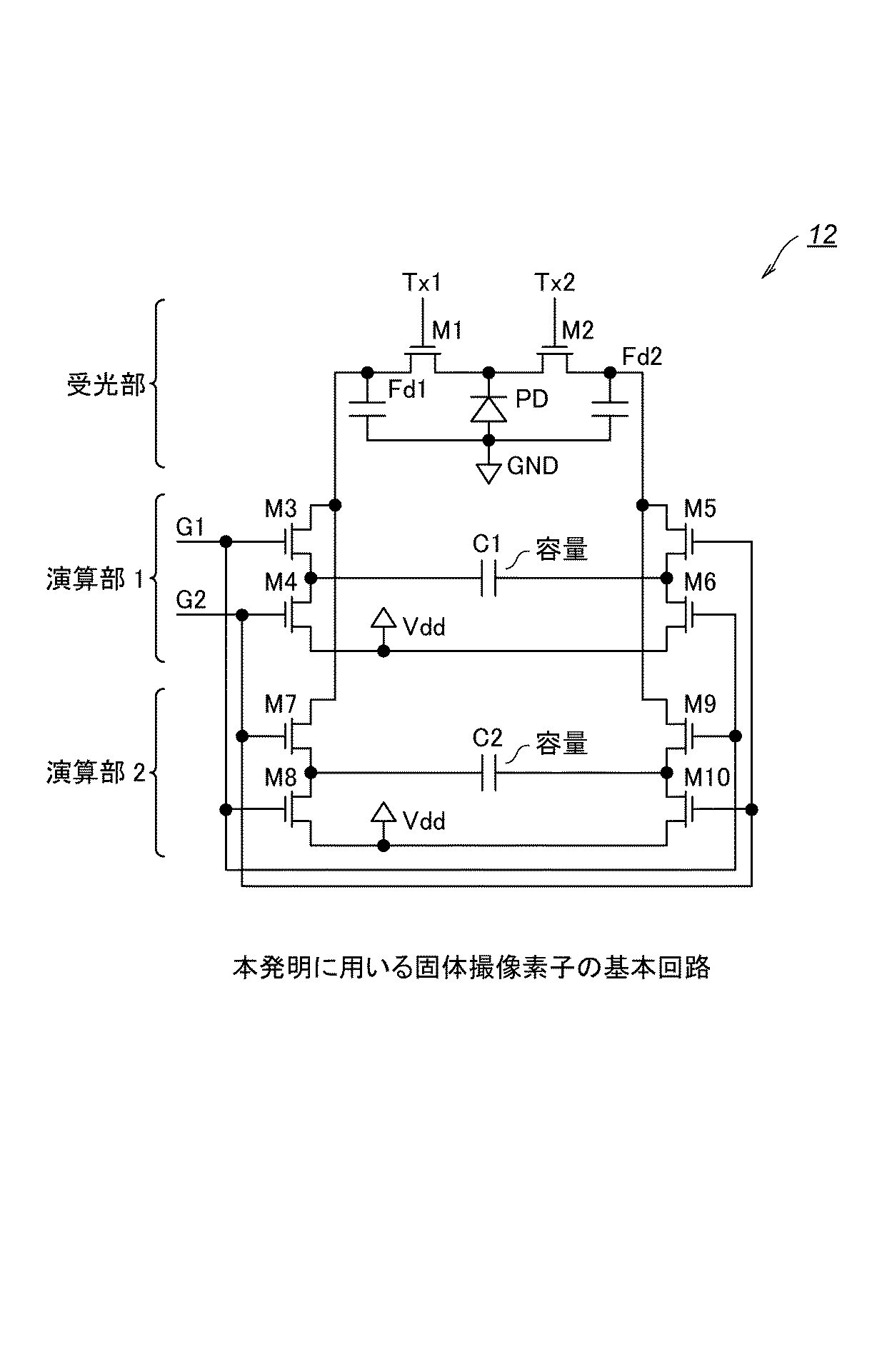
ここで、図4には、光飛行時間型距離画像センサ10の画素として用いる固体撮像素子12の基本回路の回路図が示されている。
Here, FIG. 4 shows a circuit diagram of a basic circuit of the solid-
この図4に示す固体撮像素子12は、本願出願人と同一の出願人により出願された特開2008−89346号公報に開示された発明と同一の構成を備えている。
The solid-
即ち、図4に示す固体撮像素子は、特開2008−89346号公報の図6に開示された固体撮像素子と同一の構成を備えた公知の技術であるので、その詳細な説明については特開2008−89346号公報の記載をここに援用することとし、本明細書においてはその概要について説明する。 That is, the solid-state imaging device shown in FIG. 4 is a known technique having the same configuration as the solid-state imaging device disclosed in FIG. 6 of Japanese Patent Application Laid-Open No. 2008-89346. The description in Japanese Patent Application Publication No. 2008-89346 is incorporated herein, and an outline thereof will be described in this specification.
図4に示す固体撮像素子12において、符号PDは光電変換素子であり、固体撮像素子10に入射した光は、光電変換素子PDで電荷に変換される。
In the solid-
また、符号M1、M2は、それぞれ符号Tx1、Tx2で示すゲート信号により電荷を振り分けるゲートたるFETスイッチであり、FETスイッチM1、M2の駆動により、電荷蓄積部Fd1、Fd2に、変調光に同期して電荷を振り分ける。 Reference numerals M1 and M2 denote FET switches that are gates for distributing charges according to gate signals indicated by reference numerals Tx1 and Tx2, respectively, and the charge storage units Fd1 and Fd2 are synchronized with the modulated light by driving the FET switches M1 and M2. Distribute charges.
さらに、符号M3、M4、M5、M6、M7、M8、M9、M10は、ゲート信号G1、G2により駆動され、電荷蓄積部Fd1、Fd2の電荷を、符号C1、C2で示す電荷を蓄積する容量に振り分ける。 Further, the symbols M3, M4, M5, M6, M7, M8, M9, and M10 are driven by the gate signals G1 and G2, and are capacitors that store the charges indicated by the symbols C1 and C2 in the charge storage portions Fd1 and Fd2. Sort out.
図5には、上記した図4に示す固体撮像素子12を制御するタイミングをあらわすタイミングチャートが示されている。
FIG. 5 shows a timing chart showing the timing for controlling the solid-
ゲート信号Tx1、Tx2は、同期制御部104の同期信号に従ってオン(ON)/オフ(OFF)制御され、光源102によって照射された変調光L1の変調と同期させて、入射光L2による電荷を振り分ける。
The gate signals Tx1 and Tx2 are ON / OFF controlled according to the synchronization signal of the
この際に、入射光L2のなかの変調光L1由来の反射光たる変調光成分の電荷は、電荷蓄積部Fd1と電荷蓄積部Fd2とへ位相に応じた量が振り分けられるため、電荷蓄積部Fd1と電荷蓄積部Fd2とでは蓄積する電荷の量が異なるが、入射光L2のなかの背景光由来の反射光たる背景光成分の電荷は、電荷蓄積部Fd1と電荷蓄積部Fd2とへ均等に振り分けられ、電荷蓄積部Fd1と電荷蓄積部Fd2とでは蓄積する電荷の量は一致する。 At this time, the charge of the modulated light component, which is the reflected light derived from the modulated light L1 in the incident light L2, is distributed to the charge storage unit Fd1 and the charge storage unit Fd2 according to the phase, so that the charge storage unit Fd1 The charge accumulation unit Fd2 differs in the amount of accumulated charge, but the background light component of reflected light derived from background light in the incident light L2 is equally distributed to the charge accumulation unit Fd1 and the charge accumulation unit Fd2. Thus, the charge storage units Fd1 and Fd2 have the same amount of stored charge.
なお、本明細書においては、上記した「電荷蓄積部Fd1と電荷蓄積部Fd2とに電荷を振り分けて蓄積する時間」を「光蓄積時間」と適宜に称する。 In the present specification, the “time for distributing and storing charges in the charge storage portion Fd1 and the charge storage portion Fd2” is appropriately referred to as “light storage time”.
さらに、ゲート信号G1をオンするとともにゲート信号G2をオフした状態を正接続期間とすると、光蓄積時間における正接続期間では、電荷蓄積部Fd1の電荷は、図4における容量C1の左端へ、また、電荷蓄積部Fd2の電荷は、図4における容量C2の右端に移動する。 Further, when the state in which the gate signal G1 is turned on and the gate signal G2 is turned off is a positive connection period, in the positive connection period in the light accumulation time, the charge in the charge storage portion Fd1 is transferred to the left end of the capacitor C1 in FIG. The charge in the charge storage unit Fd2 moves to the right end of the capacitor C2 in FIG.
ここで、ゲート信号G1をオフするとともにゲート信号G2をオンさせる。この状態を反転接続期間とすると、この光蓄積時間における反転接続期間では、電荷蓄積部Fd1の電荷は、図4における容量C2の左端へ、また、電荷蓄積部Fd2の電荷は、図4における容量C1の右端に蓄積し、正接続期間にたまった電荷を打ち消す働きをする。 Here, the gate signal G1 is turned off and the gate signal G2 is turned on. When this state is an inversion connection period, in the inversion connection period in this optical storage time, the charge in the charge storage portion Fd1 is to the left end of the capacitor C2 in FIG. 4, and the charge in the charge storage portion Fd2 is in the capacity in FIG. It accumulates at the right end of C1 and functions to cancel out the charges accumulated in the positive connection period.
より詳細には、最初に、ゲート信号Tx1、Tx2、G1、G2の全てをオンにする。この最初に全てのゲート信号Tx1、Tx2、G1、G2をオンする時間を、リセット期間Rと称することとする。
More specifically, first, all of the gate signals Tx1, Tx2, G1, and G2 are turned on. The time at which all the gate signals Tx1, Tx2, G1, and G2 are turned on first is referred to as a reset period R.
このリセット期間Rにおいては、FETスイッチM1〜M10の全てが接続されるので、電荷蓄積部Fd1、Fd2の端子はVdd電位と等しくなる。また、光電変換素子PDの電位は、ゲート信号Tx1、Tx2の電圧に従ったポテンシャルにリセットされ、容量C1、C2は、放電した状態にリセットされる。 In the reset period R, since all of the FET switches M1 to M10 are connected, the terminals of the charge storage units Fd1 and Fd2 become equal to the Vdd potential. Further, the potential of the photoelectric conversion element PD is reset to a potential according to the voltages of the gate signals Tx1 and Tx2, and the capacitors C1 and C2 are reset to a discharged state.
なお、上記した各リセットは、光飛行時間型センサ10の各画素の属するラインの画面の読み出しの最初に行うものである。
Each reset described above is performed at the beginning of reading the screen of the line to which each pixel of the optical time-of-
上記したリセットを終了すると、次回にリセットするまで、光電変換素子PDが光を受光することにより発生した光電子の電荷を変調光L1に同期して振り分け蓄積するため、高速なパルス信号たるゲート信号Tx1、Tx2を印加し、また、正接続期間と反転接続期間とが交互に存在するようにゲート信号G1、G2を印加する。 When the above-described reset is completed, the charge of the photoelectrons generated by the photoelectric conversion element PD receiving light is distributed and accumulated in synchronization with the modulated light L1 until the next reset, so that the gate signal Tx1 which is a high-speed pulse signal , Tx2 are applied, and the gate signals G1, G2 are applied so that the positive connection period and the inversion connection period exist alternately.
なお、正接続期間および反転接続期間は等しい時間であり、ゲート信号Tx1、Tx2による高速パルスの整数倍の時間とする。 Note that the positive connection period and the inversion connection period are the same time, which is an integral multiple of the high-speed pulse by the gate signals Tx1 and Tx2.
図6には、上記した操作で変調光成分を残したまま、背景光を除去する様子をあらわした図が示されている。
FIG. 6 is a diagram showing how the background light is removed while leaving the modulated light component in the above operation.
なお、図6におけるΔQFD1は、正接続期間に電荷蓄積部Fd1に対して流入した電荷を表し、また、図6におけるΔQFD2は、正接続期間に電荷蓄積部Fd2に流入した電荷を表す。 Note that ΔQFD1 in FIG. 6 represents the charge flowing into the charge storage unit Fd1 during the positive connection period, and ΔQFD2 in FIG. 6 represents the charge flowed into the charge storage unit Fd2 during the positive connection period.
正接続期間と反転接続期間とを等しい時間にすると、電荷蓄積部Fd1と電荷蓄積部Fd2とに等しく蓄積した背景光成分は相殺されるが、変調光成分は電荷蓄積部Fd1と電荷蓄積部Fd2とに位相に応じた比率で蓄積しているため、容量C1と容量C2とには電荷蓄積部Fd1と電荷蓄積部Fd2との差分成分だけが残ることになる。 When the positive connection period and the inversion connection period are equal, the background light components stored equally in the charge storage unit Fd1 and the charge storage unit Fd2 are canceled out, but the modulated light component is the charge storage unit Fd1 and the charge storage unit Fd2. Therefore, only the difference component between the charge storage unit Fd1 and the charge storage unit Fd2 remains in the capacitors C1 and C2.
本発明による光飛行時間型距離画像センサの制御方法は、上記したように、固体撮像素子12の容量C1と容量C2とには電荷蓄積部Fd1と電荷蓄積部Fd2との差分成分だけが残ることに鑑みて、電荷蓄積部Fd1と電荷蓄積部Fd2とに蓄積される背景光成分の割合たるゲインを任意の値に設定することにより、変調光成分は残したままで、電荷蓄積部Fd1と電荷蓄積部Fd2とに蓄積される背景光成分を任意の割合で削減することを可能にしたものである。
In the control method of the time-of-flight distance image sensor according to the present invention, as described above, only the difference component between the charge storage unit Fd1 and the charge storage unit Fd2 remains in the capacitor C1 and the capacitor C2 of the solid-
次に、本発明による光飛行時間型距離画像センサの制御方法について、図7を参照しながら説明する。
Next, a method for controlling the time-of-flight distance image sensor according to the present invention will be described with reference to FIG.
図7において、符号T1で示す期間は正接続期間であり、符号T2で示す期間は反転接続期間であるが、正接続期間T1と反転接続期間T2との時間間隔が図7に示すものとなるようにゲート信号G1、G2を印加することにより、図5に示す場合におけると比較すると、電荷蓄積部Fd1と電荷蓄積部Fd2とに蓄積される背景光成分による電荷を1/2、即ち、半分に削減することができる。 In FIG. 7, the period indicated by reference numeral T1 is a positive connection period, and the period indicated by reference numeral T2 is an inverting connection period, but the time interval between the positive connection period T1 and the inverting connection period T2 is as shown in FIG. By applying the gate signals G1 and G2 as described above, the charge due to the background light component accumulated in the charge accumulation portion Fd1 and the charge accumulation portion Fd2 is halved, that is, half as compared with the case shown in FIG. Can be reduced.
具体的には、図7に場合においては、最初の正接続期間T1と最初の正接続期間T1に続く反転接続期間T2とは等しい時間間隔であるが、当該反転接続期間T2に続く正接続期間T1は、当該反転接続期間T2の2倍の時間間隔であり、反転接続期間を設けない時のゲインを1とすると、そのゲインを「0.5」にすることができる。 Specifically, in the case of FIG. 7, the first positive connection period T1 and the reverse connection period T2 following the first positive connection period T1 are equal in time interval, but the positive connection period following the reverse connection period T2 T1 is a time interval twice as long as the inversion connection period T2. If the gain when the inversion connection period is not provided is 1, the gain can be set to “0.5”.
つまり、図7に示す例は、背景光成分のゲインを0.5としたときのゲート信号G1、G2の駆動の様子を示すものであり、最初の正接続期間T1の期間に蓄積した背景光成分の電荷は、反転接続期間T2の期間で相殺され、2回目の正接続期間T1の期間に蓄積された背景光成分の電荷のみが残ることになる。このとき、「T1:T2=3:1」である。 That is, the example shown in FIG. 7 shows how the gate signals G1 and G2 are driven when the gain of the background light component is 0.5, and the background light accumulated during the first positive connection period T1. The component charge is canceled during the inversion connection period T2, and only the background light component charge accumulated during the second positive connection period T1 remains. At this time, “T1: T2 = 3: 1”.
このようにすると、蓄積する背景光成分の電荷は2分の1になるが、上記したように、変調光成分の電荷は相殺されずにそのまま残る。 In this way, the charge of the background light component to be accumulated is halved, but as described above, the charge of the modulated light component remains without being canceled.
これにより、距離画像の距離精度に関係する変調光成分の電荷を減らすことなく、背景光成分のダイナミックレンジを上げることができるものである。 Thereby, the dynamic range of the background light component can be increased without reducing the charge of the modulated light component related to the distance accuracy of the distance image.
また、図8には、他のゲインの例として、背景光成分のゲインを0.25としたときのゲート信号G1、G2の駆動の様子が示されている。このとき、「T1:T2=5:3」である。 FIG. 8 shows another example of the gain, in which the gate signals G1 and G2 are driven when the gain of the background light component is 0.25. At this time, “T1: T2 = 5: 3”.
ここで、あるゲインgに設定するときの正接続期間T1と反転接続期間T2との比は、下記の数式4で求められる。
なお、上記した図7や図8に示す駆動方法はあくまで一例であり、T1:T2の比が変わらなければ、電荷蓄積部Fd1、Fd2が飽和しない限り、どのようなタイミングでゲート信号G1、G2を制御してもよい。
Note that the driving methods shown in FIGS. 7 and 8 are merely examples. If the ratio of T1: T2 does not change, the gate signals G1, G2 can be used at any timing unless the charge storage units Fd1, Fd2 are saturated. May be controlled.
上記したようにゲート信号G1、G2を任意の時間比で切り替え制御することにより、変調光成分の電荷は電荷蓄積部Fd1、Fd2に残したままで、背景光成分の電荷のみを電荷蓄積部Fd1、Fd2から減少させることができることになる。 By switching and controlling the gate signals G1 and G2 at an arbitrary time ratio as described above, the charge of the modulated light component remains in the charge storage units Fd1 and Fd2, and only the charge of the background light component remains in the charge storage unit Fd1, It can be decreased from Fd2.
そして、図3に示す光飛行時間型距離画像センサ10は、上記において説明した本発明による光飛行時間型距離画像センサの制御方法により、距離画像生成部108によって生成された距離画像に応じて、上記したゲインを自動的に可変する制御システムを備えたている。
Then, the optical time-of-flight
なお、この図3に示す光飛行時間型距離画像センサ10において、距離画像生成部108によって距離画像を生成する際の処理については、「背景技術」の項において説明した光飛行時間型距離画像センサ100と同様であるので、その詳細な説明は省略する。
In the optical time-of-flight
ここで、図9には、光飛行時間型距離画像センサ10においてゲインを自動的に可変する制御の処理ルーチンたるゲイン制御ルーチンのフローチャートが示されている。
Here, FIG. 9 shows a flowchart of a gain control routine which is a processing routine of control for automatically changing the gain in the optical time-of-flight
このゲイン制御ルーチンは、光飛行時間型距離画像センサ10により距離画像を取得する動作が起動されると、その動作中においては所定の時間間隔(例えば、30分の1秒毎である。)で繰り返し起動されて実行され、ゲインの調整が自動的に行われる。
In the gain control routine, when an operation for acquiring a distance image is started by the optical time-of-flight
即ち、光飛行時間型距離画像センサ10により距離画像を取得する動作が起動されて、その動作中において所定の時間間隔でゲイン制御ルーチンが起動されると、画素カウント部14は、距離画像生成部108が生成した距離画像を取得し(ステップS902)、取得した距離画像の画素の中から第1の閾値として設定された所定の輝度値(例えば、輝度値が0〜255の時、240である。)以上の画素の数を計数(カウント)する(ステップS904)。
That is, when an operation for acquiring a distance image is started by the optical time-of-flight
上記したステップS904の処理を終了すると、ステップS906の処理へ進み、ゲイン制御部16は、ステップS904の処理でカウントした画素の数が第1の所定値以上(例えば、全画素の10%以上である。)であるか否かを判断する。
When the process of step S904 is completed, the process proceeds to step S906, and the
このステップS906の判断処理において、ステップS904の処理でカウントした画素の数が第1の所定値以上ではないと判断された場合には、ステップS907の処理へ進み、取得した距離画像の画素の中から第2の閾値として設定された所定の輝度値(例えば、輝度値が0〜255の時、15である。)以下の画素の数を計数(カウント)する。 In the determination process of step S906, when it is determined that the number of pixels counted in the process of step S904 is not equal to or greater than the first predetermined value, the process proceeds to the process of step S907, and among the pixels of the acquired distance image. The number of pixels below a predetermined luminance value set as the second threshold value (for example, 15 when the luminance value is 0 to 255) is counted (counted).
上記したステップS907の処理を終了すると、ステップS908の処理へ進み、ゲイン制御部16は、ステップS907の処理でカウントした画素の数が第2の所定値以上(例えば、全画素の10%以上)であるか否かを判断する。
When the process of step S907 is finished, the process proceeds to step S908, and the
このステップS908の判断処理において、ステップS907の処理でカウントした画素の数が第2の所定値以上ではないと判断された場合には、ステップS910の処理へ進み、ゲインの変更は行わない。 If it is determined in step S908 that the number of pixels counted in step S907 is not equal to or greater than the second predetermined value, the process proceeds to step S910, and the gain is not changed.
一方、ステップS908の判断処理において、ステップS907の処理でカウントした画素の数が第2の所定値以上であると判断された場合には、ステップS912の処理へ進み、ゲインを上げるようにしてゲインの変更を行う。 On the other hand, in the determination process of step S908, if it is determined that the number of pixels counted in the process of step S907 is equal to or greater than the second predetermined value, the process proceeds to the process of step S912 to increase the gain. Make changes.
なお、このステップS912の処理でゲインを上げる際には、例えば、0.05だけゲインを上げるようにする。 When increasing the gain in the process of step S912, for example, the gain is increased by 0.05.
また、ステップS906の判断処理において、ステップS904の処理でカウントした画素の数が第1の所定値以上であると判断された場合には、ステップS914の処理へ進み、ゲインを下げるようにしてゲインの変更を行う。 If it is determined in step S906 that the number of pixels counted in step S904 is greater than or equal to the first predetermined value, the process proceeds to step S914 to reduce the gain. Make changes.
なお、このステップS914の処理でゲインを下げる際には、例えば、0.05だけゲインを下げるようにする。 Note that when the gain is lowered in the process of step S914, the gain is lowered by, for example, 0.05.
そして、上記したステップS910、ステップS912あるいはステップS914の処理を終了すると、これによりゲインの調整の処理を完了し(ステップS916)、このゲイン制御ルーチンを終了して、次のゲイン制御ルーチンの起動を待つ。 When the processing in step S910, step S912, or step S914 described above is completed, the gain adjustment processing is completed thereby (step S916), the gain control routine is terminated, and the next gain control routine is started. wait.
従って、上記した光飛行時間型距離画像センサ10においては、上記において説明した本発明による光飛行時間型距離画像センサの制御方法により、距離画像生成部108によって生成された距離画像に応じて、上記したゲインを自動的に可変することができることになる。
Therefore, in the optical time-of-flight
次に、図10には、本発明の第2の実施の形態による光飛行時間型距離画像センサの制御方法を実施する光飛行時間型距離画像センサのブロック構成説明図が示されている。
Next, FIG. 10 shows a block configuration explanatory diagram of an optical time-of-flight distance image sensor that implements the control method of the optical time-of-flight distance image sensor according to the second embodiment of the present invention.
この図10に示す光飛行時間型距離画像センサ20は、光源102と、同期制御部104と、光を電荷に変換する光電変換素子と該光電変換素子ごとに設けられた複数の電荷蓄積部と該複数の電荷蓄積部に電荷を振り分ける振り分け手段とを有して構成された電荷振り分け方式による固体撮像素子12(上記した光飛行時間型距離画像センサ10における固体撮像素子12と同一の構成ならびに作用を備える。)と、距離画像生成部108と、距離画像生成部108により生成された距離画像のヒストグラムを作成するヒストグラム作成部22と、ヒストグラム作成部22によって作成されたヒストグラムに基づいて固体撮像素子12の電荷蓄積部に蓄積される背景光成分の電荷の割合たるゲインを制御するゲイン制御部16とを有して構成されている。
The optical time-of-flight
なお、図10に示す光飛行時間型距離画像センサ20においては、図3に示す光飛行時間型距離画像センサ10と同様に、説明を簡易化して理解を容易にするために、1個の固体撮像素子12を備えるように図示したが、実際の光飛行時間型距離画像センサにおいては、1個の固体撮像素子を1画素として、複数の固体撮像素子が2次元平面上にアレイ状に配置されて構成されている。
In the optical time-of-flight
また、ヒストグラムとは、画像における輝度(明るさ)の分布をグラフ表示したものであり、どの明るさの画素が、どれだけ存在するかをあわらすものである。 The histogram is a graph display of the luminance (brightness) distribution in the image, and indicates how many pixels of which brightness exist.
そして、この図10に示す光飛行時間型距離画像センサ20は、上記において説明した本発明による光飛行時間型距離画像センサの制御方法により、距離画像生成部108によって生成された距離画像に応じて、上記したゲインを自動的に可変する制御システムを備えたている。
The optical time-of-flight
なお、この図10に示す光飛行時間型距離画像センサ20において、距離画像生成部108によって距離画像を生成する際の処理については、「背景技術」の項において説明した光飛行時間型距離画像センサ100と同様であるので、その詳細な説明は省略する。
In the optical time-of-flight
ここで、図11には、光飛行時間型距離画像センサ20においてゲインを自動的に可変する制御の処理ルーチンたるゲイン制御ルーチンのフローチャートが示されている。
Here, FIG. 11 shows a flowchart of a gain control routine, which is a control processing routine for automatically varying the gain in the optical time-of-flight
このゲイン制御ルーチンは、光飛行時間型距離画像センサ20により距離画像を取得する動作の起動されると、その動作中においては所定の時間間隔(例えば、30分の1秒毎である。)で繰り返し起動されて実行され、ゲインの調整が自動的に行われる。
In the gain control routine, when an operation for acquiring a distance image by the optical time-of-flight
即ち、光飛行時間型距離画像センサ20により距離画像を取得する動作が起動されて、その動作中において所定の時間間隔でゲイン制御ルーチンが起動されると、ヒストグラム作成部22は、距離画像生成部108が生成した距離画像を取得し(ステップS1002)、取得した距離画像のヒストグラムを作成する(ステップS1004)。
That is, when an operation for acquiring a distance image is started by the optical time-of-flight
上記したステップS1004の処理を終了すると、ステップS1006の処理へ進み、ゲイン制御部24は、ステップS1004の処理で取得したヒストグラムが第1の規定値(例えば、標準偏差が15以内で、かつ、輝度値の平均が200以上である。)より明るいか否かを判断する。
When the process of step S1004 is completed, the process proceeds to step S1006, and the
このステップS1006の判断処理において、ステップS1004の処理で取得したヒストグラムが第1の規定値より明るくないと判断された場合には、ステップS1008の処理へ進み、ステップS1004の処理で取得したヒストグラムが第2の規定値(例えば、標準偏差が15以下で、かつ、輝度値の平均が55以下である。)より暗いか否かを判断する。 If it is determined in step S1006 that the histogram acquired in step S1004 is not brighter than the first specified value, the process proceeds to step S1008, and the histogram acquired in step S1004 is the first histogram. It is determined whether or not it is darker than a specified value of 2 (for example, the standard deviation is 15 or less and the average luminance value is 55 or less).
このステップS1008の判断処理において、ステップS1004の処理で取得したヒストグラムが第2の規定値より暗くないと判断された場合には、ステップS1010の処理へ進み、ゲインの変更は行わない。 If it is determined in step S1008 that the histogram acquired in step S1004 is not darker than the second specified value, the process proceeds to step S1010, and the gain is not changed.
一方、ステップS1008の判断処理において、ステップS1004の処理で取得したヒストグラムが第2の規定値より暗いと判断された場合には、ステップS1012の処理へ進み、ゲインを上げるようにしてゲインの変更を行う。 On the other hand, in the determination process of step S1008, when it is determined that the histogram acquired in the process of step S1004 is darker than the second specified value, the process proceeds to step S1012 and the gain is changed by increasing the gain. Do.
なお、このステップS1012の処理でゲインを上げる際には、例えば、0.05だけゲインを上げるようにする。 Note that when the gain is increased in the process of step S1012, the gain is increased by, for example, 0.05.
また、ステップS1006の判断処理において、ステップS1004の処理で取得したヒストグラムが第1の規定値より明るいと判断された場合には、ステップS1014の処理へ進み、ゲインを下げるようにしてゲインの変更を行う。 If it is determined in step S1006 that the histogram acquired in step S1004 is brighter than the first specified value, the process proceeds to step S1014, and the gain is changed by decreasing the gain. Do.
なお、このステップS1014の処理でゲインを下げる際には、例えば、0.05だけゲインを下げるようにする。 Note that when the gain is lowered in the process of step S1014, the gain is lowered by, for example, 0.05.
そして、上記したステップS1010、ステップS1012あるいはステップS1014の処理を終了すると、これによりゲインの調整の処理を完了し(ステップS1016)、このゲイン制御ルーチンを終了し、次のゲイン制御ルーチンの起動を待つ。 When the processing in step S1010, step S1012 or step S1014 is completed, the gain adjustment processing is completed (step S1016), the gain control routine is terminated, and the next gain control routine is awaited. .
従って、上記した光飛行時間型距離画像センサ20においては、上記において説明した本発明による光飛行時間型距離画像センサの制御方法により、距離画像生成部108によって生成された距離画像に応じて、上記したゲインを自動的に可変することができることになる。
Therefore, in the optical time-of-flight
以上において説明したように、上記した本発明による第1の実施の形態ならびに第2の実施の形態によれば、距離画像を求めるのに必要な変調光成分による電荷を残したままで、背景光成分の電荷を任意の量だけ除去できるため、距離画像の距離精度を落とすことなく、ダイナミックレンジの広い輝度画像を同時に得ることができるようになる。
As described above, according to the first embodiment and the second embodiment of the present invention described above, the background light component is left while leaving the charge due to the modulated light component necessary for obtaining the distance image. Therefore, a luminance image with a wide dynamic range can be obtained simultaneously without reducing the distance accuracy of the distance image.
なお、上記した実施の形態は、以下の(1)乃至(4)に示すように変形することができるものである。
The embodiment described above can be modified as shown in the following (1) to (4).
(1)上記した第1の実施の形態ならびに第2の実施の形態において、ゲイン制御ルーチンは、所定の時間間隔で繰り返し起動して実行されることに限られるものではなく、光飛行時間型距離画像センサ10、20のユーザーが、任意のタイミングで起動して実行させるようにしてもよい。
(1) In the first embodiment and the second embodiment described above, the gain control routine is not limited to being repeatedly activated and executed at a predetermined time interval. The user of the
(2)上記した第1の実施の形態において、第1の所定値と第2の所定値とは、互いに異なる値でもよいし、あるいは、同一の値でもよい。 (2) In the first embodiment described above, the first predetermined value and the second predetermined value may be different from each other, or may be the same value.
(3)上記した第2の実施の形態において、第1の規定値と第2の規定値とは、互いに異なる値でもよいし、あるいは、同一の値でもよい。 (3) In the second embodiment described above, the first specified value and the second specified value may be different from each other or the same value.
(4)上記した実施の形態ならびに上記した(1)乃至(3)に示す変形例は、適宜に組み合わせるようにしてもよい。 (4) You may make it combine suitably the embodiment shown above and the modification shown in said (1) thru | or (3).
本発明は、自動車などに搭載して、障害物までの距離を測定する光飛行時間型距離画像センサなどに利用することができるものである。 The present invention can be used for an optical time-of-flight distance image sensor that is mounted on an automobile or the like and measures the distance to an obstacle.
10、20、100 光飛行時間型距離画像
12、106 固体撮像素子
14 画素カウント部
16、24 ゲイン制御部
22 ヒストグラム生成部
102 光源
104 同期制御部
108 距離画像生成部
200 対象物体
10, 20, 100 Time-of-
Claims (4)
前記光電変換素子ごとに設けられるとともに、前記光電変換素子により変換された電荷を蓄積可能な複数の電荷蓄積部と、
前記変調光に同期して、前記光電変換素子により変換された電荷を前記複数の電荷蓄積部に振り分けて、前記複数の電荷蓄積部に電荷を蓄積させる振り分け手段と、
前記複数の電荷蓄積部とそれぞれ導通可能な複数の容量と、
前記複数の電荷蓄積部と前記複数の容量との導通状態を制御する制御手段と
を有する固体撮像素子により、画素を構成した光飛行時間型距離画像センサの制御方法であって、
ある時間に撮像された画像から所定の輝度値の画素の数をカウントし、
該カウントした画素の数に基づいて、前記変調光以外の光による電荷を前記複数の電荷蓄積部から除去する割合を決定し、
前記振り分け手段により前記複数の電荷蓄積部に電荷を振り分ける光蓄積時間において、該決定した割合に基づいて、前記制御手段により制御される導通状態を切り替えることにより、前記変調光による電荷を前記複数の電荷蓄積部に蓄積させたまま、前記変調光以外の光による電荷を該決定した割合で前記複数の電荷蓄積部から除去する
ことを特徴とする光飛行時間型距離画像センサの制御方法。 A photoelectric conversion element that converts light including modulated light into electric charge;
A plurality of charge storage units provided for each photoelectric conversion element and capable of storing charges converted by the photoelectric conversion element;
A distribution unit configured to distribute the charge converted by the photoelectric conversion element to the plurality of charge storage units in synchronization with the modulated light, and to store the charges in the plurality of charge storage units;
A plurality of capacitors each capable of conducting with the plurality of charge storage units;
A control method of a time-of-flight distance image sensor in which a pixel is formed by a solid-state imaging device having a control unit that controls conduction between the plurality of charge storage units and the plurality of capacitors,
Count the number of pixels with a given luminance value from an image captured at a certain time,
Based on the counted number of pixels, determine a ratio of removing charges from light other than the modulated light from the plurality of charge storage units,
By switching the conduction state controlled by the control unit based on the determined ratio in the light accumulation time for distributing the charge to the plurality of charge storage units by the distribution unit, the charge due to the modulated light is changed to the plurality of charge storage units. A method of controlling a time-of-flight distance image sensor, wherein charges due to light other than the modulated light are removed from the plurality of charge storage units at the determined ratio while being stored in a charge storage unit.
前記光電変換素子ごとに設けられるとともに、前記光電変換素子により変換された電荷を蓄積可能な複数の電荷蓄積部と、
前記変調光に同期して、前記光電変換素子により変換された電荷を前記複数の電荷蓄積部に振り分けて、前記複数の電荷蓄積部に電荷を蓄積させる振り分け手段と、
前記複数の電荷蓄積部とそれぞれ導通可能な複数の容量と、
前記複数の電荷蓄積部と前記複数の容量との導通状態を制御する制御手段と
を有する固体撮像素子により、画素を構成した光飛行時間型距離画像センサの制御方法であって、
ある時間に撮像された画像からヒストグラムを作成し、
該作成したヒストグラムに基づいて、前記変調光以外の光による電荷を前記複数の電荷蓄積部から除去する割合を決定し、
前記振り分け手段により前記複数の電荷蓄積部に電荷を振り分ける光蓄積時間において、該決定した割合に基づいて、前記制御手段により制御される導通状態を切り替えることにより、前記変調光による電荷を前記複数の電荷蓄積部に蓄積させたまま、前記変調光以外の光による電荷を該決定した割合で前記複数の電荷蓄積部から除去する
ことを特徴とする光飛行時間型距離画像センサの制御方法。 A photoelectric conversion element that converts light including modulated light into electric charge;
A plurality of charge storage units provided for each photoelectric conversion element and capable of storing charges converted by the photoelectric conversion element;
A distribution unit configured to distribute the charge converted by the photoelectric conversion element to the plurality of charge storage units in synchronization with the modulated light, and to store the charges in the plurality of charge storage units;
A plurality of capacitors each capable of conducting with the plurality of charge storage units;
A control method of a time-of-flight distance image sensor in which a pixel is formed by a solid-state imaging device having a control unit that controls conduction between the plurality of charge storage units and the plurality of capacitors,
Create a histogram from images taken at a certain time,
Based on the created histogram, determine a ratio of removing charges from light other than the modulated light from the plurality of charge storage units,
By switching the conduction state controlled by the control unit based on the determined ratio in the light accumulation time for distributing the charge to the plurality of charge storage units by the distribution unit, the charge due to the modulated light is changed to the plurality of charge storage units. A method of controlling a time-of-flight distance image sensor , wherein charges due to light other than the modulated light are removed from the plurality of charge storage units at the determined ratio while being stored in a charge storage unit.
前記光電変換素子ごとに設けられるとともに、前記光電変換素子により変換された電荷を蓄積可能な複数の電荷蓄積部と、
前記変調光に同期して、前記光電変換素子により変換された電荷を前記複数の電荷蓄積部に振り分けて、前記複数の電荷蓄積部に電荷を蓄積させる振り分け手段と、
前記複数の電荷蓄積部とそれぞれ導通可能な複数の容量と、
前記複数の電荷蓄積部と前記複数の容量との導通状態を制御する制御手段と
を有する固体撮像素子により、画素を構成した光飛行時間型距離画像センサの制御システムであって、
ある時間に撮像された画像から所定の輝度値の画素の数をカウントするカウント手段と、
前記カウント手段がカウントした画素の数に基づいて、前記変調光以外の光による電荷を前記複数の電荷蓄積部から除去する割合を決定するゲイン調整手段と
を有し、
前記制御手段が、前記振り分け手段により前記複数の電荷蓄積部に電荷を振り分ける光蓄積時間において、前記ゲイン調整手段が決定した割合に基づいて、前記導通状態を切り替えることにより、
前記変調光による電荷を前記複数の電荷蓄積部に蓄積させたまま、前記変調光以外の光による電荷を前記ゲイン調整手段が決定した割合で前記複数の電荷蓄積部から除去する
ことを特徴とする光飛行時間型距離画像センサの制御システム。 A photoelectric conversion element that converts light including modulated light into electric charge;
A plurality of charge storage units provided for each photoelectric conversion element and capable of storing charges converted by the photoelectric conversion element;
A distribution unit configured to distribute the charge converted by the photoelectric conversion element to the plurality of charge storage units in synchronization with the modulated light, and to store the charges in the plurality of charge storage units;
A plurality of capacitors each capable of conducting with the plurality of charge storage units;
A control system for a time-of-flight distance image sensor comprising pixels by a solid-state imaging device having control means for controlling a conduction state between the plurality of charge storage units and the plurality of capacitors,
Counting means for counting the number of pixels having a predetermined luminance value from an image captured at a certain time;
Gain adjusting means for determining a ratio of removing charges due to light other than the modulated light from the plurality of charge storage units based on the number of pixels counted by the counting means;
By switching the conduction state based on the ratio determined by the gain adjusting means in the light accumulation time in which the control means distributes the charges to the plurality of charge accumulation units by the distribution means,
The charge due to light other than the modulated light is removed from the plurality of charge accumulation units at a rate determined by the gain adjusting means while the charge due to the modulated light is accumulated in the plurality of charge accumulation units. Control system for optical time-of-flight range image sensor.
前記光電変換素子ごとに設けられるとともに、前記光電変換素子により変換された電荷を蓄積可能な複数の電荷蓄積部と、
前記変調光に同期して、前記光電変換素子により変換された電荷を前記複数の電荷蓄積部に振り分けて、前記複数の電荷蓄積部に電荷を蓄積させる振り分け手段と、
前記複数の電荷蓄積部とそれぞれ導通可能な複数の容量と、
前記複数の電荷蓄積部と前記複数の容量との導通状態を制御する制御手段と
を有する固体撮像素子により、画素を構成した光飛行時間型距離画像センサの制御システムであって、
ある時間に撮像された画像からヒストグラムを作成するヒストグラム作成手段と、
前記ヒストグラム作成手段が作成したヒストグラムに基づいて、前記変調光以外の光による電荷を前記複数の電荷蓄積部から除去する割合を決定するゲイン調整手段と
を有し、
前記制御手段が、前記振り分け手段により前記複数の電荷蓄積部に電荷を振り分ける光蓄積時間において、前記ゲイン調整手段が決定した割合に基づいて、前記導通状態を切り替えることにより、
前記変調光による電荷を前記複数の電荷蓄積部に蓄積させたまま、前記変調光以外の光による電荷を前記ゲイン調整手段が決定した割合で前記複数の電荷蓄積部から除去する
ことを特徴とする光飛行時間型距離画像センサの制御システム。 A photoelectric conversion element that converts light including modulated light into electric charge;
A plurality of charge storage units provided for each photoelectric conversion element and capable of storing charges converted by the photoelectric conversion element;
A distribution unit configured to distribute the charge converted by the photoelectric conversion element to the plurality of charge storage units in synchronization with the modulated light, and to store the charges in the plurality of charge storage units;
A plurality of capacitors each capable of conducting with the plurality of charge storage units;
A control system for a time-of-flight distance image sensor comprising pixels by a solid-state imaging device having control means for controlling a conduction state between the plurality of charge storage units and the plurality of capacitors,
A histogram creation means for creating a histogram from an image captured at a certain time;
Gain adjusting means for determining a ratio of removing charges from light other than the modulated light from the plurality of charge storage units based on the histogram created by the histogram creating means;
By switching the conduction state based on the ratio determined by the gain adjusting means in the light accumulation time in which the control means distributes the charges to the plurality of charge accumulation units by the distribution means,
The charge due to light other than the modulated light is removed from the plurality of charge accumulation units at a rate determined by the gain adjusting means while the charge due to the modulated light is accumulated in the plurality of charge accumulation units. Control system for optical time-of-flight range image sensor .
Priority Applications (1)
| Application Number | Priority Date | Filing Date | Title |
|---|---|---|---|
| JP2008240240A JP5271643B2 (en) | 2008-09-19 | 2008-09-19 | Control method and system for optical time-of-flight range image sensor |
Applications Claiming Priority (1)
| Application Number | Priority Date | Filing Date | Title |
|---|---|---|---|
| JP2008240240A JP5271643B2 (en) | 2008-09-19 | 2008-09-19 | Control method and system for optical time-of-flight range image sensor |
Publications (2)
| Publication Number | Publication Date |
|---|---|
| JP2010071832A JP2010071832A (en) | 2010-04-02 |
| JP5271643B2 true JP5271643B2 (en) | 2013-08-21 |
Family
ID=42203756
Family Applications (1)
| Application Number | Title | Priority Date | Filing Date |
|---|---|---|---|
| JP2008240240A Active JP5271643B2 (en) | 2008-09-19 | 2008-09-19 | Control method and system for optical time-of-flight range image sensor |
Country Status (1)
| Country | Link |
|---|---|
| JP (1) | JP5271643B2 (en) |
Families Citing this family (10)
| Publication number | Priority date | Publication date | Assignee | Title |
|---|---|---|---|---|
| JP5781918B2 (en) * | 2011-12-28 | 2015-09-24 | 浜松ホトニクス株式会社 | Distance measuring device |
| CN103581645B (en) | 2012-07-24 | 2017-05-24 | 三星电子株式会社 | Depth sensing apparatus and method |
| KR102007279B1 (en) | 2013-02-08 | 2019-08-05 | 삼성전자주식회사 | Depth pixel included in three-dimensional image sensor, three-dimensional image sensor including the same and method of operating depth pixel included in three-dimensional image sensor |
| KR102003496B1 (en) | 2013-03-06 | 2019-10-01 | 삼성전자주식회사 | Image Sensor and Image Pick Up Apparatus |
| JP6590517B2 (en) * | 2015-05-12 | 2019-10-16 | スタンレー電気株式会社 | Distance image generator |
| WO2016208214A1 (en) | 2015-06-24 | 2016-12-29 | 株式会社村田製作所 | Distance sensor |
| CN106331442B (en) | 2015-07-02 | 2021-01-15 | 松下知识产权经营株式会社 | Image pickup apparatus |
| KR20170048972A (en) | 2015-10-27 | 2017-05-10 | 삼성전자주식회사 | Apparatus and Method for generating image |
| EP3589990A4 (en) * | 2017-03-01 | 2021-01-20 | Ouster, Inc. | ACCURATE PHOTODESTECTOR MEASUREMENTS FOR LIDAR |
| US11105925B2 (en) | 2017-03-01 | 2021-08-31 | Ouster, Inc. | Accurate photo detector measurements for LIDAR |
Family Cites Families (6)
| Publication number | Priority date | Publication date | Assignee | Title |
|---|---|---|---|---|
| JP2000287121A (en) * | 1999-03-30 | 2000-10-13 | Fuji Film Microdevices Co Ltd | Image signal processor |
| JP3938833B2 (en) * | 2000-04-27 | 2007-06-27 | 株式会社リコー | Exposure control device |
| JP4235729B2 (en) * | 2003-02-03 | 2009-03-11 | 国立大学法人静岡大学 | Distance image sensor |
| EP1614159B1 (en) * | 2003-04-11 | 2014-02-26 | Microsoft Corporation | Method and system to differentially enhance sensor dynamic range |
| JP2007170856A (en) * | 2005-12-19 | 2007-07-05 | Denso Corp | Distance data generation method, distance image generation device, photoelectric sensor |
| JP5395323B2 (en) * | 2006-09-29 | 2014-01-22 | ブレインビジョン株式会社 | Solid-state image sensor |
-
2008
- 2008-09-19 JP JP2008240240A patent/JP5271643B2/en active Active
Also Published As
| Publication number | Publication date |
|---|---|
| JP2010071832A (en) | 2010-04-02 |
Similar Documents
| Publication | Publication Date | Title |
|---|---|---|
| JP5271643B2 (en) | Control method and system for optical time-of-flight range image sensor | |
| US12287404B2 (en) | Time of flight sensor, a three-dimensional imaging device using the same, and a method for driving the three-dimensional imaging device | |
| US11863886B2 (en) | Pixel sensor having multiple photodiodes | |
| US11974044B2 (en) | Pixel sensor having adaptive exposure time | |
| US9621860B2 (en) | Image capturing apparatus and control method thereof, and storage medium | |
| US11448757B2 (en) | Distance measuring device | |
| US10477118B2 (en) | System and methods for depth imaging using conventional CCD image sensors | |
| CN107710015B (en) | Distance measuring device and distance image synthesis method | |
| US20220082698A1 (en) | Depth camera and multi-frequency modulation and demodulation-based noise-reduction distance measurement method | |
| US8767189B2 (en) | Solid state imaging device and distance image measurement device | |
| US10009554B1 (en) | Method and system for using light emission by a depth-sensing camera to capture video images under low-light conditions | |
| JP7069315B2 (en) | LED flicker reduction for video | |
| US11991341B2 (en) | Time-of-flight image sensor resolution enhancement and increased data robustness using a binning module | |
| CN110361751B (en) | Time flight depth camera and distance measuring method for reducing noise of single-frequency modulation and demodulation | |
| KR102888593B1 (en) | HDR visible light imaging using TOF pixels | |
| US20200396399A1 (en) | Non-linear quantization at pixel sensor | |
| CN105894492A (en) | T-O-F depth imaging device rendering depth image of object and method thereof | |
| CN105991933B (en) | Image Sensor | |
| JP6025081B2 (en) | Distance image sensor | |
| US20220043129A1 (en) | Time flight depth camera and multi-frequency modulation and demodulation distance measuring method | |
| CN108848320A (en) | Depth detection system and its exposure time adjusting method | |
| JP2016090436A (en) | Time-of-flight optical ranging device | |
| JP2001313958A (en) | 3D image input device | |
| US20220229189A1 (en) | Time-of-flight sensor and system | |
| JP2011029790A (en) | Imaging system |
Legal Events
| Date | Code | Title | Description |
|---|---|---|---|
| A621 | Written request for application examination |
Free format text: JAPANESE INTERMEDIATE CODE: A621 Effective date: 20110810 |
|
| A977 | Report on retrieval |
Free format text: JAPANESE INTERMEDIATE CODE: A971007 Effective date: 20130131 |
|
| A131 | Notification of reasons for refusal |
Free format text: JAPANESE INTERMEDIATE CODE: A131 Effective date: 20130212 |
|
| A521 | Request for written amendment filed |
Free format text: JAPANESE INTERMEDIATE CODE: A523 Effective date: 20130328 |
|
| TRDD | Decision of grant or rejection written | ||
| A01 | Written decision to grant a patent or to grant a registration (utility model) |
Free format text: JAPANESE INTERMEDIATE CODE: A01 Effective date: 20130423 |
|
| A61 | First payment of annual fees (during grant procedure) |
Free format text: JAPANESE INTERMEDIATE CODE: A61 Effective date: 20130513 |
|
| R150 | Certificate of patent or registration of utility model |
Free format text: JAPANESE INTERMEDIATE CODE: R150 Ref document number: 5271643 Country of ref document: JP Free format text: JAPANESE INTERMEDIATE CODE: R150 |
|
| R250 | Receipt of annual fees |
Free format text: JAPANESE INTERMEDIATE CODE: R250 |
|
| R250 | Receipt of annual fees |
Free format text: JAPANESE INTERMEDIATE CODE: R250 |
|
| R250 | Receipt of annual fees |
Free format text: JAPANESE INTERMEDIATE CODE: R250 |
|
| R250 | Receipt of annual fees |
Free format text: JAPANESE INTERMEDIATE CODE: R250 |
|
| R250 | Receipt of annual fees |
Free format text: JAPANESE INTERMEDIATE CODE: R250 |
|
| R250 | Receipt of annual fees |
Free format text: JAPANESE INTERMEDIATE CODE: R250 |
|
| R250 | Receipt of annual fees |
Free format text: JAPANESE INTERMEDIATE CODE: R250 |
|
| R250 | Receipt of annual fees |
Free format text: JAPANESE INTERMEDIATE CODE: R250 |
|
| R250 | Receipt of annual fees |
Free format text: JAPANESE INTERMEDIATE CODE: R250 |
|
| R250 | Receipt of annual fees |
Free format text: JAPANESE INTERMEDIATE CODE: R250 |