JP5164400B2 - Nonvolatile semiconductor memory device - Google Patents
Nonvolatile semiconductor memory device Download PDFInfo
- Publication number
- JP5164400B2 JP5164400B2 JP2007062017A JP2007062017A JP5164400B2 JP 5164400 B2 JP5164400 B2 JP 5164400B2 JP 2007062017 A JP2007062017 A JP 2007062017A JP 2007062017 A JP2007062017 A JP 2007062017A JP 5164400 B2 JP5164400 B2 JP 5164400B2
- Authority
- JP
- Japan
- Prior art keywords
- write
- data
- memory cell
- line
- voltage
- Prior art date
- Legal status (The legal status is an assumption and is not a legal conclusion. Google has not performed a legal analysis and makes no representation as to the accuracy of the status listed.)
- Expired - Fee Related
Links
Images


Landscapes
- Read Only Memory (AREA)
Description
この発明は、不揮発性半導体記憶装置に関し、特に、電気的に書込および消去が可能な不揮発性半導体記憶装置に関する。 The present invention relates to a nonvolatile semiconductor memory device, and more particularly to a nonvolatile semiconductor memory device that can be electrically written and erased.
不揮発的にデータを記憶する半導体記憶装置として、従来、フラッシュメモリが知られている。このフラッシュメモリにおいては、メモリセルトランジスタとして、フローティングゲートとコントロールゲートとの積層ゲート構造トランジスタを利用する。フローティングゲートの電荷(電子)の蓄積量に応じて、メモリセルトランジスタのしきい値電圧が設定され、このメモリセルのしきい値電圧に応じて、データを記憶する。 Conventionally, a flash memory is known as a semiconductor memory device that stores data in a nonvolatile manner. In this flash memory, a stacked gate structure transistor of a floating gate and a control gate is used as a memory cell transistor. The threshold voltage of the memory cell transistor is set according to the amount of charge (electrons) stored in the floating gate, and data is stored according to the threshold voltage of the memory cell.
このフローティングゲートを利用するメモリセル構造の場合、データの書込および消去には、高電圧が必要とされる。この書込/消去の電圧が高いため、メモリセルトランジスタの微細化が困難であり、また他のロジック等と同一半導体チップ上に集積化するのが困難となる。そこで、このようなフローティングゲート型メモリセル(積層ゲート型メモリセルトランジスタ)に代えて、絶縁膜に電荷を蓄積することによりデータを記憶するMONOS型メモリセルがロジック混載メモリとして利用されている。このMONOS型メモリセルの構造は、たとえば特許文献1(特開2005−347679号公報)および特許文献2(特開2002−231830号公報)に示されている。 In the case of a memory cell structure using this floating gate, a high voltage is required for writing and erasing data. Since the write / erase voltage is high, it is difficult to miniaturize the memory cell transistor, and it is difficult to integrate it on the same semiconductor chip as other logic. Therefore, instead of such a floating gate type memory cell (stacked gate type memory cell transistor), a MONOS type memory cell that stores data by accumulating charges in an insulating film is used as a logic embedded memory. The structure of this MONOS type memory cell is shown, for example, in Patent Document 1 (Japanese Patent Laid-Open No. 2005-347679) and Patent Document 2 (Japanese Patent Laid-Open No. 2002-231830).
これらの特許文献1および2に示されるように、MONOS型メモリセルは、ビット線とソース線との間に直列に接続されるメモリセルトランジスタと選択トランジスタとで構成される。選択トランジスタは、通常のMOSトランジスタ(絶縁ゲート型電界効果トランジスタ)で構成され、一方の不純物拡散領域がビット線に接続される。メモリセルトランジスタは、コントロールゲート(メモリセルゲート)、積層絶縁膜、および1つの不純物拡散層(ソース/ドレイン領域)で構成される。積層絶縁膜が、ONO膜(酸化膜−窒化膜−酸化膜)で構成される。この窒化膜内に離散的に分布するトラップに電荷を蓄積する。不純物拡散層がソース線を構成する。
As shown in these
MONOS型メモリセルにおいては、電荷トラップが窒化膜中に離散化して分布している。従って、フローティングゲート型メモリセルと異なり、電子が通過する酸化膜に局所的な欠陥が存在する場合においても、電荷は、大部分がトラップに保持される。これにより、酸化膜をフローティングゲート型メモリセルトランジスタに比べて薄くすることができ、書込電圧を低くでき、応じて素子を微細化することが可能となる。これらの特徴により、MONOS型メモリセルを有する不揮発性メモリは、ロジックとプロセスを共通化することができ、混載が容易となる。 In the MONOS type memory cell, charge traps are discretely distributed in the nitride film. Therefore, unlike the floating gate type memory cell, even when a local defect exists in the oxide film through which electrons pass, most of the charge is held in the trap. Thus, the oxide film can be made thinner than the floating gate type memory cell transistor, the write voltage can be lowered, and the element can be miniaturized accordingly. With these features, a nonvolatile memory having a MONOS type memory cell can share a logic and a process, and can be easily mixed.
また、メモリセルにおいて選択トランジスタを用いているため、このメモリセルトランジスタがデプレション型トランジスタとなっても、いわゆる「過消去」の問題が生じない。したがって、過消去を防止するためのベリファイ期間が不要となり、書込を高速化することができる(通例、書込を行う前に消去が行われる)。 Further, since the selection transistor is used in the memory cell, the so-called “over-erasure” problem does not occur even if the memory cell transistor becomes a depletion type transistor. Therefore, a verify period for preventing over-erasing is not required, and writing can be speeded up (usually, erasing is performed before writing).
このような選択トランジスタとMONOS型メモリセルトランジスタとでメモリセルが構成される場合においても、半選択状態のメモリセルに対しては、ゲートとソース/ドレインとの間に高電界が印加される。半選択状態のメモリセルとは、選択行かつ非選択列または選択列かつ非選択行にあるメモリセルを示す。この場合、トンネル電流またはホットエレクトロン/ホールにより電荷蓄積膜に対する電荷(エレクトロンまたはホール)の移動が生じ、データが損失するまたは蓄積電荷量が変化して経時的にデータが損失する「ディスターバンス」の問題が生じる。 Even in the case where a memory cell is constituted by such a selection transistor and a MONOS type memory cell transistor, a high electric field is applied between the gate and the source / drain for the half-selected memory cell. The half-selected memory cell refers to a memory cell in a selected row and a non-selected column or a selected column and a non-selected row. In this case, tunneling current or hot electrons / holes cause the movement of charges (electrons or holes) to the charge storage film, and data is lost or the stored charge amount changes and data is lost over time. Problem arises.
このようなデータの書込/消去時のディスターバンスを防止することを図る構成が、特許文献3(特開2005−276347号公報)、特許文献4(特開平9−213090号公報)、および特許文献5(特開2006−157050号公報)に示されている。 A configuration for preventing such disturbance at the time of data writing / erasing is disclosed in Patent Document 3 (Japanese Patent Laid-Open No. 2005-276347), Patent Document 4 (Japanese Patent Laid-Open No. 9-213090), and Patent Document 5 (Japanese Patent Laid-Open No. 2006-157050) discloses this.
特許文献3(特開2005−276347号公報)は、ソース線からビット線に定電流を流してデータ書込を行う不揮発性メモリにおいて、書込ディスターブを改善するための構成を示す。メモリセルは、選択トランジスタとメモリセルトランジスタとを有するスプリットゲート型メモリセルである。この特許文献3の定電流書込方式においては、選択メモリセルのしきい値電圧が大きい場合、ビット線電圧が低下し、ソース線とビット線との電圧差が大きくなる。この状態においては、選択列かつ非選択行の半選択状態のメモリセルにおいて、ソース線からビット線に電流が流れてチャネルホットエレクトロンにより誤書込が生じる可能性がある。この書込ディスターバンスを回避するために、特許文献3は、選択ビット線の電圧を所定値以上の電圧レベルに維持する。この所定値の電圧は、選択列かつ非選択行のメモリセルに書込が生じない電圧レベルである。書込が不要なかつ非選択メモリセルに書込ディスターバンスを生じさせるメモリセル、すなわちしきい値電圧の高いメモリセルに対して、選択ビット線の電圧を所定値以上に設定することにより、書込を防止する。ビット線電圧設定回路として、ソースフォロアトランジスタを利用して、ビット線の電圧の下限値を所定値に維持する。 Patent Document 3 (Japanese Patent Laid-Open No. 2005-276347) shows a configuration for improving write disturb in a nonvolatile memory in which data is written by passing a constant current from a source line to a bit line. The memory cell is a split gate type memory cell having a selection transistor and a memory cell transistor. In the constant current writing method of Patent Document 3, when the threshold voltage of the selected memory cell is large, the bit line voltage is lowered and the voltage difference between the source line and the bit line is increased. In this state, in the memory cell in the half-selected state of the selected column and non-selected row, current may flow from the source line to the bit line, and erroneous writing may occur due to channel hot electrons. In order to avoid this write disturbance, Patent Document 3 maintains the voltage of the selected bit line at a voltage level equal to or higher than a predetermined value. The voltage having the predetermined value is a voltage level at which writing does not occur in the memory cells in the selected column and the non-selected row. By setting the voltage of the selected bit line to a predetermined value or higher for a memory cell that does not require writing and causes write disturbance in a non-selected memory cell, that is, a memory cell having a high threshold voltage, To prevent it. As the bit line voltage setting circuit, a source follower transistor is used to maintain the lower limit value of the bit line voltage at a predetermined value.
選択メモリセルのしきい値電圧が低い場合、ソース線からの電流供給により、ビット線の電圧が所定値以上となる。クランプトランジスタがオフ状態となり、ビット線電圧のクランプを停止する。非選択メモリセルにおいては、ソース線とビット線との電圧差が小さく、リーク電流によるホットエレクトロンの発生は回避され、誤書込が防止される。選択メモリセルに対しては定電流が流れ、書込が行われる。 When the threshold voltage of the selected memory cell is low, the voltage of the bit line becomes equal to or higher than a predetermined value by supplying current from the source line. The clamp transistor is turned off, and the clamping of the bit line voltage is stopped. In the non-selected memory cell, the voltage difference between the source line and the bit line is small, the generation of hot electrons due to the leakage current is avoided, and erroneous writing is prevented. A constant current flows through the selected memory cell, and writing is performed.
選択メモリセルのしきい値電圧が高い場合、ビット線の電圧が所定値以下となる。この場合、クランプトランジスタがオン状態となり、ビット線電圧を所定値にクランプする。この状態においては、ビット線には定電流がクランプトランジスタを介して供給され、選択メモリセルにおいては定電流が流れない。これにより、選択メモリセルのしきい値電圧が高い場合、選択メモリセルに対する書込が回避される。すなわち、選択列において、ビット線を書込阻止電圧のレベルに設定し、またソース線を書込定電流供給電圧レベルに設定する。これにより、半選択メモリセルにおいてソース線からビット線に対して流れる電流を抑制し、書込ディスターバンスを抑制する。 When the threshold voltage of the selected memory cell is high, the voltage of the bit line becomes a predetermined value or less. In this case, the clamp transistor is turned on, and the bit line voltage is clamped to a predetermined value. In this state, a constant current is supplied to the bit line via the clamp transistor, and no constant current flows in the selected memory cell. Thereby, when the threshold voltage of the selected memory cell is high, writing to the selected memory cell is avoided. That is, in the selected column, the bit line is set to the level of the write inhibition voltage, and the source line is set to the write constant current supply voltage level. Thereby, the current flowing from the source line to the bit line in the half-selected memory cell is suppressed, and the write disturbance is suppressed.
特許文献4(特開平9−213090号公報)は、フローティングゲート型メモリセルにおけるドレインディスターバンスを回避する構成を開示する。ドレインディスターバンスでは、以下の現象が生じる。選択ビット線に接続される非選択メモリセルにおいて、ドレイン(ビット線に接続される不純物領域)とコントロールゲートの間の高電界により、電子/正孔対がウィークアバランシェにより生成され、正孔がフローティングゲートに注入され、また、ドレイン高電界によりフローティングゲートからドレインに電子がトンネル電流により引抜かれる。これにより、書込状態の非選択メモリセルのしきい値電圧が低下する。また、消去状態のメモリセルにおいては、フローティングゲートの電圧が、容量結合によりビット線電圧の上昇に伴って上昇し、チャネルが形成され、電子が流れる。ドレイン高電界によるアバランシェ効果により電子/正孔対を生成する。非選択ワード線の電圧レベルに応じて、正孔がフローティングゲートに注入され、しきい値電圧がさらに低下するか、逆に、電子がフローティングゲートに注入され、しきい値電圧が高くなる。 Japanese Patent Laid-Open No. 9-213090 discloses a configuration for avoiding drain disturbance in a floating gate type memory cell. In the drain disturbance, the following phenomenon occurs. In an unselected memory cell connected to the selected bit line, a high electric field between the drain (impurity region connected to the bit line) and the control gate generates electron / hole pairs by weak avalanche, and the holes float. Electrons are injected into the gate, and electrons are extracted from the floating gate to the drain by a tunnel current due to the high electric field of the drain. As a result, the threshold voltage of the unselected memory cell in the written state is lowered. Further, in the erased memory cell, the voltage of the floating gate rises as the bit line voltage rises due to capacitive coupling, a channel is formed, and electrons flow. Electron / hole pairs are generated by the avalanche effect due to the drain high electric field. Depending on the voltage level of the unselected word line, holes are injected into the floating gate and the threshold voltage is further lowered, or conversely, electrons are injected into the floating gate and the threshold voltage is increased.
この特許文献4は、このようなドレインディスターバンスを回避するために、非選択ワード線および非選択ソース線に書込電圧Vppの1/2倍の電圧VPP/2を印加する。この場合においても、選択列かつ非選択行の消去状態のメモリセルにおいて、ビット線電圧の上昇に伴ってチャネル電流が流れる。この半選択状態の消去状態のメモリセルの数が増大するとビット線電圧が低下する。これを防止するために非選択ソース線の電圧を単に電圧VPP/2に設定する場合では、書込が遅くなるという問題が生じる。このため、特許文献4は、さらに、ソース線をワード線と平行に配置する。選択行のワード線を書込高電圧、ソース線を接地電圧に設定する。非選択行については、ワード線を中間電圧VPP/2に設定し、ソース線をオープン状態に設定する。ビット線についても、選択列のビット線を高電圧に設定し、非選択ビット線をオープン状態に設定する。選択列かつ非選択行のメモリセルにおいてワード線電圧が中間電圧レベルでありドレイン高電界を緩和して、書込状態のメモリセルに対する正孔の注入を抑制する。また、非選択行のソース線をオープン状態に設定することにより、消去状態のメモリセルにおいてチャネル電流を制限して、電子/正孔対の生成を抑制する。
In
特許文献5(特開2006−157050号公報)は、ONO膜を電荷蓄積手段として利用するメモリセルにおいて、書込ディスターバンスを低減することを目的とする構成を開示する。この特許文献5においては、ビット線とソース線とが平行に配置されるアレイ構成において、選択行においてワード線に書込高電圧、非選択行のワード線に対してメモリセルトランジスタのチャネル領域に対して逆バイアス状態となる電圧を印加し、非選択列のビット線およびソース線に対してチャネル領域に対して逆バイアスとなる電圧を印加する。この特許文献5は、非選択列のビット線の書込阻止電圧の上限を、非選択ワード線電圧および非選択ソース線の電圧により高くして書込ディスターバンスを改善することを図る。非選択メモリセルにおいて、基板領域における空乏層の拡大によるトンネル電流を抑制しまた垂直方向の電界を緩和して、電荷蓄積膜に対する電荷の移動を抑制する。
MONOS型メモリトランジスタおよび選択トランジスタを有するスプリットゲートMONOSセルにおいては、特許文献3の定電流書込方式と異なり、定電圧バイアス方式の書込がある。この定電圧バイアス書込方式においては、選択列のソース線およびビット線に書込電圧を伝達し、この電圧差に従ってチャネル電流を流す。このチャネル電流のホットエレクトロンを電荷蓄積膜に注入する。非選択メモリセルの書込阻止は、非選択ビット線の電圧を、メモリセルの選択トランジスタのコントロールゲート線上の電圧以上に設定することにより行なわれる。選択トランジスタのコントロールゲート(ワード線)およびソース(ビット線)を逆バイアス状態として、選択トランジスタを深いオフ状態とする。また、非選択メモリセルについては、メモリゲート線MGは、バンド間トンネル電流によるホットホール注入が生じるのを防止するためおよび非選択状態から選択状態までの遷移時間を短縮するため、接地電圧と書込選択電圧との間の電圧レベルに設定される。これにより、非選択メモリセルにおいて選択トランジスタを介してチャネル電流が流れてホットエレクトロンまたはホットホールが生じるのを防止する。 In the split gate MONOS cell having the MONOS type memory transistor and the selection transistor, there is a constant voltage bias type writing unlike the constant current writing method of Patent Document 3. In this constant voltage bias write method, a write voltage is transmitted to the source line and bit line of the selected column, and a channel current is caused to flow according to this voltage difference. Hot electrons of this channel current are injected into the charge storage film. The non-selected memory cell is prevented from being written by setting the voltage of the non-selected bit line to be equal to or higher than the voltage on the control gate line of the selection transistor of the memory cell. The control gate (word line) and source (bit line) of the selection transistor are set in a reverse bias state, and the selection transistor is set in a deep off state. For the non-selected memory cell, the memory gate line MG is written as a ground voltage in order to prevent hot hole injection due to the band-to-band tunnel current and to shorten the transition time from the non-selected state to the selected state. Is set to a voltage level between the first and second select voltages. This prevents a channel current from flowing through the selection transistor in the non-selected memory cell to cause hot electrons or hot holes.
携帯機器などの用途においては、アプリケーションプログラムおよびダウンロードデータの格納などのために、大記憶容量が要求され、また、電池を電源とするため、低消費電力性能が要求される。また、高速読出を行なうために、ビット線負荷を軽減することが要求される。また、ソース線が列方向に延在して配置されるアレイ構成においては、ソース線が不純物領域(拡散層)で構成され、その抵抗値が増大すると、抵抗によりソース線電圧が変化し、各メモリセルに対して正確にソース線電圧を設定することが困難となる。これらの理由により、列方向のメモリセルの増加が抑制される。したがって、通例、1行のメモリセルの数を増大させて記憶容量を増大する。このアレイ構成において、メモリセル全てのソース線に対して並行に書込電圧を伝達して書込を行なう場合、ソース線書込電圧を生成する回路の消費電力が大きくなり、また、駆動能力を大きくするために回路の占有面積が増大する(トランジスタのサイズを大きくするため)。上述のように、MONOS型メモリセルにおいては、ソース線が不純物領域で構成され、ビット線などのメタル配線に比べて、その接合容量等により負荷が大きい。高速でソース線を駆動するためには、ソース線駆動回路の電流駆動力は大きくする必要があり、メモリセル数の増大とともに、ソース線駆動回路の消費電流およびレイアウト面積の増大の問題が顕著になる。 In applications such as portable devices, a large storage capacity is required for storing application programs and download data, and a low power consumption performance is required because a battery is used as a power source. Further, in order to perform high-speed reading, it is required to reduce the bit line load. In an array configuration in which source lines extend in the column direction, the source lines are constituted by impurity regions (diffusion layers), and when the resistance value increases, the source line voltage changes due to the resistance. It becomes difficult to set the source line voltage accurately for the memory cell. For these reasons, an increase in memory cells in the column direction is suppressed. Therefore, the storage capacity is usually increased by increasing the number of memory cells in one row. In this array configuration, when writing is performed by transmitting the write voltage in parallel to the source lines of all the memory cells, the power consumption of the circuit for generating the source line write voltage is increased, and the drive capability is increased. To increase the size, the area occupied by the circuit increases (to increase the size of the transistor). As described above, in the MONOS type memory cell, the source line is constituted by an impurity region, and the load is larger than the metal wiring such as the bit line due to its junction capacitance. In order to drive the source line at high speed, it is necessary to increase the current driving capability of the source line driving circuit, and as the number of memory cells increases, the problem of increase in current consumption and layout area of the source line driving circuit becomes remarkable. Become.
また、書込時において、全ビット線に並行して書込電圧を伝達すると、書込電流が大きくなり、ビット線書込電圧生成回路およびソース線駆動回路の負荷が大きくなる。これを回避するため、ビット線毎に書込電圧を順次伝達して、メモリセルへの書込を実行する。すなわち、いわゆる「ページモード」に従ってデータの書込を実行する。この場合においても、1ワード線に接続されるメモリセルの数が増大した場合、1ワード線のメモリセル全体に対する書込時間が長くなる。応じて、選択行において、非選択列のメモリセルがディスターバンスを受ける時間が長くなり、データの信頼性が低下する問題が生じる。 In writing, if a write voltage is transmitted in parallel to all the bit lines, the write current increases, and the load on the bit line write voltage generation circuit and the source line drive circuit increases. In order to avoid this, the write voltage is sequentially transmitted to each bit line, and writing to the memory cell is executed. That is, data writing is executed according to a so-called “page mode”. Also in this case, if the number of memory cells connected to one word line increases, the writing time for the entire memory cell of one word line becomes longer. Accordingly, in the selected row, the time during which the memory cells in the non-selected columns are disturbed becomes longer, and there is a problem that the reliability of data is lowered.
したがって、メモリ容量が増大した場合、書込時にメモリセルがディスターバンスを受ける時間が長くなり、データ保持特性が劣化するという問題が生じる。 Therefore, when the memory capacity is increased, there is a problem that the time during which the memory cell is disturbed at the time of writing becomes longer and the data retention characteristic is deteriorated.
上述の特許文献1においては、単に、電荷蓄積膜のシリコン窒化膜の電荷トラップサイトを低減して電荷保持特性を改善するために、シリコン窒化膜の製造工程を改善することを検討しているだけであり、データ書込時のディスターバンスの問題については何ら考慮していない。
In the above-mentioned
特許文献2は、コントロールゲート線に対して自己整合的に側壁に形成されるメモリセルゲート線に対するコンタクトを正確にかつ安定に形成することを考慮しているだけであり、何ら、書込時のメモリセルのディスターバンスについては考慮していない。 Patent Document 2 only considers forming a contact to the memory cell gate line formed on the side wall in a self-aligned manner with respect to the control gate line accurately and stably. The memory cell disturbance is not taken into consideration.
特許文献3に示される構成においては、定電流方式でデータを書込んでいる。ビット線電圧を書込阻止電圧レベルに設定し、選択メモリセルのしきい値電圧に従って選択的に選択メモリセルに定電流を供給している。この場合、選択列/非選択行のメモリセルにおいて、書込ディスターバンスを回避する。しかしながら、定電圧バイアスでソース線からビット線に電流を流す構成に対しては、この特許文献3の構成を適用することはできない。また、この特許文献3は、選択行/非選択列のメモリセルのディスターバンスについては考慮していない。また、ソース線を全て同時に選択状態としても良いことが記載されている。しかしながら、ソース線負荷によるソース線電流駆動回路の電流駆動力の問題については何ら考慮していない。また、ページモードでの高速かつ安定なデータ書込については、何ら考慮していない。単に1ビットのメモリセルに対するデータの書込が検討されているだけである。 In the configuration shown in Patent Document 3, data is written by a constant current method. The bit line voltage is set to the write inhibition voltage level, and a constant current is selectively supplied to the selected memory cell according to the threshold voltage of the selected memory cell. In this case, write disturb is avoided in the memory cells in the selected column / non-selected row. However, the configuration of Patent Document 3 cannot be applied to a configuration in which current flows from the source line to the bit line with a constant voltage bias. Further, this Patent Document 3 does not consider the disturbance of the memory cells in the selected row / non-selected column. It also describes that all the source lines may be selected at the same time. However, no consideration is given to the problem of the current driving capability of the source line current driving circuit due to the source line load. Further, no consideration is given to high-speed and stable data writing in the page mode. Only writing data to a 1-bit memory cell is being considered.
特許文献4は、選択列かつ非選択行のメモリセルのディスターバンスを問題とする。選択行/非選択列のメモリセルのディスターバンスについては何ら考慮していない。特に、スプリットゲート型メモリセルにおいては、ソース線がメモリセルトランジスタのドレイン領域として機能するため、選択行かつ非選択列のドレインディスターバンスの問題が大きくなる。この特許文献4においては、従来例の問題を解決するために、ソース線をワード線と平行に設けている。ソース線毎にその電位/状態を設定する必要があり、ソース線毎にソース線スイッチ回路またはソース線駆動回路を配置する必要がある。このため、メモリセルアレイにおいて、行方向のレイアウト面積が増大する。特に、メモリアレイ構造としては、複数のメモリブロックが設けられ、ワード線がメモリブロック間で分離される。消去をワード線単位またはブロック単位で実行される。従って、メモリブロックのレイアウト面積が増大し、小占有面積の不揮発性半導体記憶装置を実現するのが困難となる。
また、この特許文献4の構成において、選択行かつ非選択列のメモリセルに対しては、ビット線がフローティング状態とされる。従って、ワード線とビット線との容量結合によりビット線電圧が上昇する可能性がある。この状態においては、選択行のソース線は接地電圧レベルであり、チャネル電流が流れ、ソース線とワード線との間の高電界により電子/正孔対が生成されて、フローティングゲートに電子が注入されるまたは正孔がソース線に流出するディスターバンスが生じる。、特許文献4は、このような選択行かつ非選択列のメモリセルのディスターバンスの問題は何ら考慮していない。
In the configuration of
さらに、この特許文献4は、その従来構成において、ワード線単位のブロックごとにソース線電位を制御して、非選択ブロックのソース線電圧に対して書込防止電圧を供給する構成を示す。しかしながら、この従来例においては、選択ブロックにおいて選択行(ワード線)かつ非選択列のメモリセルは、コントロールゲートとソース線との間に高電界が印加されるため、ドレインディスターバンスを抑制するのは困難である。また、メモリブロックの各メモリセルのソース線を並行して駆動するため、ソース線を書込電圧レベルに駆動する場合のソース線駆動回路の消費電流については、何ら考慮していない。また、この特許文献4は、ソース線をビット線と平行に配置したメモリセルアレイ構成におけるドレインディスターバンスをさらに抑制する構成は示していない。
Further,
特許文献5は、非選択列のビット線の書込阻止電圧の上限を非選択ワード線電圧および非選択ソース線の電圧により高くして書込ディスターバンスを改善することを図る。この特許文献5の構成においては、基板領域からフローティングゲートへ電荷の注入を行う。この基板領域全面からの電荷注入のために、選択行かつ非選択列のメモリセルに対して弱い書込が生じるディスターバンスが発生する。このディスターバンスを確実に抑制するために、特許文献5は、チャネル領域の接合バイアスを逆バイアスとして、非選択メモリセルの空乏層の広がりによりトンネル電流を抑制し、また垂直方向の電界を緩和する。
特許文献5は、選択列毎、すなわちソース線およびビット線毎に電圧を設定して、書込を行なっているものの、いわゆるページモードでデータの書込を行う構成については考慮していない。また、1本のソース線に複数列のメモリセルが共通に接続される構成において、選択行かつ非選択列のメモリセルの書込ディスターバンスを低減する構成については何ら考慮していない。また、書込時に、選択列のソース線および非選択列のソース線にそれぞれ書込電圧および書込防止電圧を印加するため、各列ごとにソース線駆動回路が必要となり、回路占有面積が増大する。
In
それゆえ、この発明の目的は、記憶容量増大時においても、書込ディスターバンスを抑制して正確かつ安定にデータの書込を行なうことができるとともに、回路占有面積および消費電力の増大を抑制することのできる不揮発性半導体記憶装置を提供することである。 Therefore, it is an object of the present invention to suppress writing disturbance and to write data accurately and stably even when the storage capacity is increased, and to suppress an increase in circuit occupation area and power consumption. It is an object of the present invention to provide a non-volatile semiconductor memory device that can be used.
この発明に係る不揮発性半導体記憶装置は、要約すれば、ビット線およびソース線が平行に配置されるとともに複数列のメモリセルが1本のソース線に共通に結合されるアレイ構成において、ソース線を単位として、データの書込を行なうものである。この場合、ビット線は、対応のソース線の選択/非選択に拘わらず並行して書込データに応じて書込電圧レベルおよび書込阻止電圧レベルに選択的に設定されてもよい。これに代えて、ビット線は、選択状態のソース線に対応するビット線のみに対し、並行して書込データに応じた書込を行なってもよく、また順次、選択ソース線に対応するビット線を書込データに応じて書込状態に設定してもよい。 The nonvolatile semiconductor memory device according to the present invention can be summarized as a source line in an array configuration in which bit lines and source lines are arranged in parallel and a plurality of columns of memory cells are commonly coupled to one source line. Data is written in units of. In this case, the bit line may be selectively set to the write voltage level and the write inhibition voltage level according to the write data in parallel regardless of the selection / non-selection of the corresponding source line. Alternatively, the bit line may be written in accordance with the write data in parallel only to the bit line corresponding to the selected source line, and the bit line corresponding to the selected source line in turn. The line may be set to a write state according to the write data.
ソース線単位でデータの書込を行なう。非選択ソース線は、非選択電圧レベルに維持される。すなわち、1実施の形態において、選択行において、コントロールゲート線およびメモリゲート線を選択状態に維持した状態で、ソース線を順次選択状態へ駆動して、ビット線へ書込データに応じて書込電圧を所定のシーケンスで伝達する。ソース線非選択電圧とビット線書込阻止電圧とは同一電圧レベルである。 Data is written in units of source lines. Unselected source lines are maintained at unselected voltage levels. That is, in one embodiment, in the selected row, with the control gate line and the memory gate line maintained in the selected state, the source lines are sequentially driven to the selected state, and the bit lines are written according to the write data. The voltage is transmitted in a predetermined sequence. The source line non-selection voltage and the bit line write inhibition voltage are at the same voltage level.
したがって、選択行かつ非選択列において、たとえば仮に、ソース線が選択状態であってビット線に書込阻止電圧が伝達された場合、この書込阻止電圧は、ソース線選択電圧以下の電圧であり、リーク電流が、ソース線からビット線方向へ流れる。選択トランジスタは、このコントロールゲート線の電圧に従って弱い反転状態であり高抵抗状態である。このディスターバンス電圧ストレスは、対応のソース線が選択状態の期間だけ印加される。したがって、この選択行かつ非選択列のメモリセルがディスターバンスを受ける期間を短くすることができる。 Therefore, in the selected row and non-selected column, for example, if the source line is in a selected state and a write inhibition voltage is transmitted to the bit line, this write inhibition voltage is a voltage equal to or lower than the source line selection voltage. A leak current flows from the source line to the bit line. The select transistor is in a weak inversion state and a high resistance state according to the voltage of the control gate line. This disturbance voltage stress is applied only during a period in which the corresponding source line is selected. Therefore, the period during which the memory cells in the selected row and the non-selected column are subjected to disturbance can be shortened.
また、1つの実施の形態において、ソース線選択時に、ビット線単位で書込電圧(書込選択電圧)を順次ビット線に伝達する場合、選択行において非選択列のメモリセルについては、ビット線の書込阻止電圧とソース線非選択電圧とは同一電圧レベルである。従って、ソース線とビット線との間には電流は流れず、ディスターバンスが生じるのは抑制される。これにより、選択行においてディスターバンスを受けるメモリセルの数を低減することができ、データの保持特性を保証することができる。 In one embodiment, when a source line is selected, when a write voltage (write selection voltage) is sequentially transmitted to a bit line in units of bit lines, a bit line is used for a memory cell in a non-selected column in a selected row. The write block voltage and the source line non-select voltage are at the same voltage level. Therefore, no current flows between the source line and the bit line, and the occurrence of disturbance is suppressed. As a result, the number of memory cells that receive disturbance in the selected row can be reduced, and data retention characteristics can be guaranteed.
また、ソース線単位でデータの書込を行なっており、ソース線を駆動する回路の消費電流は、全ソース線を並行して選択状態へ駆動する場合に比べて十分小さくすることができる。従って、メモリ容量が増大に対しても、ソース線駆動回路のレイアウト面積を増大させることは要求されない。小占有面積かつ低消費電力のソース線駆動回路を利用して高速かつ安定にデータ書込を行うことができる。 In addition, since data is written in units of source lines, the current consumption of the circuit for driving the source lines can be sufficiently reduced as compared with the case where all the source lines are driven to the selected state in parallel. Therefore, it is not required to increase the layout area of the source line driver circuit even if the memory capacity increases. Data writing can be performed stably at high speed using a source line driver circuit having a small occupation area and low power consumption.
また、ソース線は、複数列のメモリセルに対して1本設けられる。従って、各列に対応してソース線駆動回路を配置する必要がなく、レイアウト面積の増大は抑制される。 One source line is provided for a plurality of columns of memory cells. Therefore, it is not necessary to arrange a source line driver circuit corresponding to each column, and an increase in layout area is suppressed.
[実施の形態1]
図1は、この発明において用いられる不揮発性メモリセルの断面構造を概略的に示す図である。図1において、メモリセルMCは、半導体基板領域1表面に間をおいて形成される不純物領域2aおよび2b(第1および第2導通ノード)と、これらの不純物領域2aおよび2bの間の基板領域上にゲート絶縁膜3を介して形成されるコントロールゲート電極4と、ゲート絶縁膜3およびコントロールゲート電極4に隣接してL字型に形成される電荷蓄積膜5と、電荷蓄積膜5上に形成されるメモリゲート電極6を含む。
[Embodiment 1]
FIG. 1 schematically shows a cross-sectional structure of a nonvolatile memory cell used in the present invention. In FIG. 1, memory cell MC includes
電荷蓄積膜5は、基板領域1上に形成されるボトム酸化膜5aと、ボトム酸化膜5a上に形成される窒化膜5bと、窒化膜5b上に形成されるトップ酸化膜5cを含む。ボトム酸化膜5aおよびトップ酸化膜5cの間に窒化膜5bを配置し、この窒化膜5bに電荷を蓄積する。トップ酸化膜5cにより窒化膜5bとメモリゲート電極6との間の電荷のリークを抑制する。
The
不純物領域2a、ゲート絶縁膜3、およびコントロールゲート電極4により、選択トランジスタSTが形成される。電荷蓄積膜5、不純物領域2bおよびメモリゲート電極6により、メモリセルトランジスタMTが形成される。これらの選択トランジスタSTおよびメモリセルトランジスタMTが直列に接続される。メモリセルMCの選択時、メモリセルトランジスタMTのしきい値電圧に応じて選択的に不純物領域2aおよび2bの間にチャネルが形成される。
The select transistor ST is formed by the
通常、不純物領域2aが列方向に延在して形成され、1列のメモリセルに共通に配置される上層のビット線に電気的に接続される。不純物領域2bが列方向に連続的に延在して、1列のメモリセルに共通なソース線を形成する。コントロールゲート電極4は、行方向に延在するコントロールゲート線に接続される。コントロールゲート線に、1行に整列して配置されるメモリセルの選択トランジスタのコントロールゲート電極が共通に接続される。メモリゲート電極6は、同様、行方向に延在するメモリゲート線に接続される。メモリゲート線に、1行に整列して配置されるメモリセルのメモリゲート電極が共通に接続される。
Usually,
図1に示すメモリセルMCは、選択トランジスタのコントロールゲート電極4がメモリゲート電極6よりも先に形成される。従って、シリコン基板界面(半導体基板領域)の品質のよい状態で、選択ゲートトランジスタのゲート絶縁膜を、同一半導体基板上に形成されるロジック部のゲート絶縁膜と同一工程で形成することができる。メモリセルトランジスタMTにおいてはフローティングゲートが用いられていないため、トランジスタ製造工程を、同一半導体チップ上に形成されるロジックのトランジスタと共通化することができる。以下の説明においては、選択トランジスタSTおよびメモリセルトランジスタMTが、ともにNチャネルトランジスタであるとする。
In the memory cell MC shown in FIG. 1, the
この図1に示すメモリセルMCにおいて、データの書込時においては、メモリゲート電極6に11V程度の電圧が印加され、不純物領域2bに5V程度の電圧が印加される。コントロールゲート電極4へは、選択トランジスタSTのしきい値電圧よりも少し高いレベル(たとえば1V)の電圧が与えられる。不純物領域2aには、コントロールゲート電極4の電圧よりも少し低い電圧(0.8V)が印加される。この状態においては、選択トランジスタSTにおいて、ゲート絶縁膜3下部に弱い反転層が形成される。メモリセルトランジスタMTは、強いオン状態であリ、不純物領域2bから不純物領域2aに向かって電流が流れる。
In the memory cell MC shown in FIG. 1, when data is written, a voltage of about 11 V is applied to the memory gate electrode 6 and a voltage of about 5 V is applied to the
チャネル領域において、選択トランジスタSTとメモリセルトランジスタMTの境界部は高抵抗状態であり、この領域において高電界が発生する。この高電界により、不純物領域2aから不純物領域2bに流れる電子が、ホットエレクトロンとなり、メモリゲート電極6の高電圧に引かれて、電荷蓄積膜5の窒化膜5bに注入されて蓄積される。メモリセルトランジスタMTにおいては、ソース側から電子が注入されるため、ソースサイド注入方式で電子が注入され、トンネル電流を利用する構成に比べて高効率で、電子を注入することができる。この書込状態は、メモリセルトランジスタMTのしきい値電圧が高い状態に対応する。
In the channel region, the boundary between the select transistor ST and the memory cell transistor MT is in a high resistance state, and a high electric field is generated in this region. Due to this high electric field, electrons flowing from the
消去動作時においては、メモリゲート電極6にたとえば−5Vの負の高電圧が印加され、不純物領域2bに7V程度の正の高電圧が印加される。消去時においても、選択トランジスタは、コントロールゲート電極4が例えば1V、不純物領域2a(ビット線)が例えば0.8Vの電圧レベルに設定される。電流が不純物領域2bから不純物領域2aに向かって流れる。不純物領域2bの端部において高電界(ドレイン高電界)が発生し、ホットホールが生成される。メモリゲート電極6の負電圧により、バンド間トンネリング電流がボトム酸化膜5aを介して電荷蓄積膜5の窒化膜5bに流れ、ホットホールが窒化膜5bに注入されて蓄積される。これにより、書込時に注入された電子を中和して、消去状態とする。この消去状態は、メモリセルトランジスタMTのしきい値電圧が低い状態に対応する。
In the erase operation, a negative high voltage of, for example, −5V is applied to memory gate electrode 6, and a positive high voltage of about 7V is applied to
データ読出時においては、メモリゲート電極6および選択コントロールゲート電極4をそれぞれ例えば1.5Vの読出電圧レベルに設定し、不純物領域2aに1V程度の読出電圧を供給し、不純物領域2bを接地電圧レベルに設定する。不純物領域2a(ビット線)から不純物領域2b(ソース線)に流れる電流の大小により、メモリセルMCの記憶データを判定する。
At the time of data reading, memory gate electrode 6 and select
このメモリセルトランジスタMTは、一例として、消去時においてはそのしきい値電圧は負の値であっても良い。したがって、たとえメモリセルトランジスタMTが、しきい値電圧が負となる過消去状態となっても、選択トランジスタSTがオフ状態であれば、電流が流れず、他のメモリセルの読出に対して影響は及ぼさない。 For example, the memory cell transistor MT may have a negative threshold voltage at the time of erasing. Therefore, even if the memory cell transistor MT is in an over-erased state in which the threshold voltage is negative, if the selection transistor ST is in the off state, no current flows, which affects the reading of other memory cells. Does not reach.
なお、メモリセルトランジスタMTの消去状態および書込状態のいずれにおいても、メモリセルトランジスタMTのしきい値電圧が、正の電圧であっても良い。データ読出時に、書込および消去状態を識別することの電流がビット線(不純物領域2a)に流れ、この電流差が読出回路(センスアンプ)により検知することができればよい。
Note that the threshold voltage of the memory cell transistor MT may be a positive voltage in both the erased state and the written state of the memory cell transistor MT. It is only necessary that a current for identifying the writing and erasing state flows in the bit line (
非選択メモリセルの印加電圧については、ディスターバンスの問題と関連して、後に詳細に説明する。 The applied voltage of the non-selected memory cell will be described later in detail in connection with the disturbance problem.
図2は、この発明の実施の形態1に従う不揮発性半導体記憶装置の全体の構成を概略的に示す図である。図2において、不揮発性半導体記憶装置は、メモリセルMCが行列状に配列されるメモリセルアレイ10を含む。メモリセルアレイ10においては、メモリセルMCの各列に対応してビット線BLおよびソース線SLが配置される。ソース線SLは、所定数のメモリセル列ごとに、相互接続される。メモリセルMCの各行に対応して、コントロールゲート線CGおよびメモリゲート線MGが配置される。
FIG. 2 schematically shows a whole structure of the nonvolatile semiconductor memory device according to the first embodiment of the present invention. 2, the nonvolatile semiconductor memory device includes a
メモリセルMCは、図1に示す構成を有し、メモリセルトランジスタと、選択トランジスタとを含む。コントロールゲート線CGが、メモリセルMCの選択トランジスタのコントロールゲート電極に接続され、メモリゲート線MGが、メモリセルMCのメモリセルトランジスタのメモリゲート電極に接続される。ビット線BLおよびソース線SLは、それぞれ、選択トランジスタおよびメモリセルトランジスタに結合される。このビット線BLは、上層のメタル配線で構成され、図1に示す不純物層2aに電気的に接続される。ソース線SLは、図1に示す不純物領域2bにより形成される拡散層配線である。
Memory cell MC has the configuration shown in FIG. 1, and includes a memory cell transistor and a selection transistor. Control gate line CG is connected to the control gate electrode of the select transistor of memory cell MC, and memory gate line MG is connected to the memory gate electrode of the memory cell transistor of memory cell MC. Bit line BL and source line SL are coupled to a select transistor and a memory cell transistor, respectively. The bit line BL is formed of an upper metal wiring and is electrically connected to the
不揮発性半導体記憶装置は、さらに、コントロールゲート線CGを選択するコントロールゲート線選択駆動回路12と、メモリゲート線MGを選択するメモリゲート線選択駆動回路14とを含む。コントロールゲート線選択駆動回路12は、Xアドレス信号ADXに従って、メモリセルアレイ10のアドレス指定された行に対応するコントロールゲート線CGを選択状態へ駆動する。このコントロールゲート線選択駆動回路12へは、コントロールゲート電圧Vcgが与えられる。このコントロールゲート電圧Vcgは、コントロールゲート線に伝達される電圧を示し、選択電圧レベルおよび非選択電圧レベルを有する。書込および消去時においては、コントロールゲート電圧Vcgの選択電圧レベルは、メモリセルの選択トランジスタのしきい値電圧よりも少し高い1V程度の電圧レベルである。読出時においては、このコントロールゲート電圧Vcgの選択電圧レベルは、メモリセルの選択トランジスタのしきい値電圧よりも十分高い電源電圧レベルまたは3.5V程度の電圧レベルに設定される。
The nonvolatile semiconductor memory device further includes a control gate line
メモリゲート線選択駆動回路14は、Xアドレス信号ADXに従って書込時、アドレス指定された行に対応するメモリゲート線MGを高電圧レベル(たとえば11V)に設定し、非選択行のメモリゲート線MGを、たとえば3.5Vの電圧レベルに維持する。読出時、メモリゲート線選択駆動回路14は、メモリゲート電圧Vmgを、消去状態と書込状態のしきい値電圧の間の電圧レベルに維持する。このメモリゲート電圧Vmgも、メモリゲート線に伝達される電圧を示し、選択電圧レベルおよび非選択電圧レベルを有する。
When writing according to X address signal ADX, memory gate line
なお、図2においては、図面の煩雑化を避けるために、メモリセルアレイ10に関して対向してメモリゲート線選択駆動回路14およびコントロールゲート線選択駆動回路12が配置されるように示す。しかしながら、これらの選択駆動回路12および14は、メモリセルアレイ10の一方側に互いに隣接して配置されても良い。
In FIG. 2, in order to avoid complication of the drawing, the memory gate line
この不揮発性半導体記憶装置は、さらに、データ書込時、ソース線SLを順次選択状態へ駆動するソース線選択駆動回路16と、Yアドレス信号ADYに従ってメモリセルアレイ10のアドレス指定された列を選択する列選択回路18を含む。ソース線選択駆動回路16は、ソース線電圧Vsを受け、データ書込時、メモリセルアレイ10のソース線SLを順次選択状態へ駆動する。これにより、ソース線SL単位で、データの書込を実行する。ソース線電圧Vsも、ソース線に伝達される電圧であり、書込および消去時には、書込選択電圧レベルおよび書込非選択電圧レベルを有する。読出時には、ソース線電圧Vsは、接地電圧レベルに設定される。
The nonvolatile semiconductor memory device further selects the addressed column of the
列選択回路18は、Yアドレス信号ADYに従って、このメモリセルアレイ10の選択列のビット線BLを、入出力回路22に結合する。データ書込時、入出力回路22および列選択回路18を介してビット線BL上に伝達された書込データが、データラッチ回路20によりラッチされる。データラッチ回路20は、動作電源電圧として、電圧Vdを受ける。データラッチ回路20の構成は後に詳細に説明するが、データ書込時に、メモリセルアレイ10のビット線BLに伝達される書込データを、各ビット線BLごとにラッチする。次いで、ソース線選択駆動回路16によりソース線単位でデータの書込が行なわれるとき、データラッチ回路20は、ラッチデータに従って対応のビット線BLへ、電圧Vdを伝達する。電圧Vdは、ビット線の電圧であり、書込時には、書込選択電圧および書込阻止電圧の電圧レベルを示す。本実施の形態1においては、メモリセルアレイ10内において並列して、ビット線BLは、対応の書込データに応じた電圧レベルにデータラッチ回路20により設定される。
The
この不揮発性半導体記憶装置は、さらに、外部からのコマンドCMDに従って内部動作を制御する制御回路24と、この制御回路24の制御の下に、各種電圧Vmg、Vs、VcgおよびVdを生成する内部電圧発生回路26とを含む。この内部電圧発生回路26により、動作モードに応じて、各電圧のレベルが設定される。
The nonvolatile semiconductor memory device further includes a
図3は、図2に示す不揮発性半導体記憶装置の要部の構成をより具体的に示す図である。図3において、メモリセルアレイ10においては、メモリセルMCが行列状に配列される。このメモリセルMCは、選択トランジスタSTと、メモリセルトランジスタMTとを含む。図3においては、メモリセルトランジスタMTの電荷蓄積膜を太い線で示す。
FIG. 3 is a diagram more specifically showing the configuration of the main part of the nonvolatile semiconductor memory device shown in FIG. In FIG. 3, in the
メモリセルMCの各行に対応してメモリゲート線MG0−MGnおよびコントロールゲート線CG0−CGnが設けられる。メモリゲート線MG0−MGnは、対応の行のメモリセルトランジスタMTのゲート(メモリセルゲート電極6)に接続される。コントロールゲート線CG0−CGnは、それぞれ対応の行のメモリセルMCの選択トランジスタSTのゲート(コントロールゲート電極4)に接続される。 Corresponding to each row of memory cells MC, memory gate lines MG0-MGn and control gate lines CG0-CGn are provided. Memory gate lines MG0-MGn are connected to the gate (memory cell gate electrode 6) of memory cell transistor MT in the corresponding row. Control gate lines CG0 to CGn are respectively connected to the gates (control gate electrodes 4) of the select transistors ST of the memory cells MC in the corresponding row.
メモリセル列に対応して、ビット線BL0−BLmが配設される。隣接列のメモリセルMCに共有されるように、ソース線SL0−SLkが配設される。ここで、k=m/2である。ビット線BL0−BLmは、それぞれ対応の列のメモリセルの選択トランジスタの第1の導通ノード(不純物領域)に接続される。ソース線SL0−SLkは、対応の列のメモリセルMCのメモリセルトランジスタMTの第2の導通ノード(不純物領域)に接続される。 Bit lines BL0 to BLm are provided corresponding to the memory cell columns. Source lines SL0 to SLk are arranged so as to be shared by adjacent column memory cells MC. Here, k = m / 2. Bit lines BL0 to BLm are respectively connected to the first conduction node (impurity region) of the select transistor of the memory cell in the corresponding column. Source lines SL0-SLk are connected to the second conduction node (impurity region) of memory cell transistor MT of memory cell MC in the corresponding column.
図3においては、ソース線が隣接列のメモリセルにより共有されるように示す。しかしながら、メモリセル各列に対応してローカルソース線が配設され、所定数のメモリセル列ごとにローカルソース線がコモンソース線に接続されても良い。このソース線配置の場合、コモンソース線単位でデータの書込が行われる。 In FIG. 3, the source lines are shown to be shared by adjacent columns of memory cells. However, a local source line may be provided corresponding to each column of memory cells, and the local source line may be connected to the common source line for each predetermined number of memory cell columns. In this source line arrangement, data is written in units of common source lines.
コントロールゲート線選択駆動回路12は、コントロールゲート線CG0−CGnそれぞれに対応して設けられるコントロールゲート線ドライバCDR0−CDRnを含む。これらのコントロールゲート線ドライバCDR0−CDRnは、コントロールゲート線選択駆動回路12に含まれる図示しないデコード回路からの行指定信号(デコード信号)に従って対応のコントロールゲート線に選択/非選択電圧を伝達する。コントロールゲート線ドライバCDR0−CDRnは、コントロールゲート線電圧Vcgを、動作電源電圧として受ける。
Control gate line
メモリゲート線選択駆動回路14は、メモリゲート線MG0−MGnそれぞれに対応して設けられるメモリゲート線ドライバMDR0−MDRnを含む。メモリゲート線選択駆動回路14も、図示しないデコード回路からの行指定信号(デコード信号)に従って対応のメモリゲート線へ、選択または非選択電圧レベルのメモリゲート線電圧Vmgを伝達する。
Memory gate line
ソース線選択駆動回路16は、図示しないシフトクロック信号に従ってシフト動作を行なうシフトレジスタ回路SFRと、ソース線SL0−SLkそれぞれに対応して設けられるソース線ドライバSDR0−SDRkを含む。このシフトレジスタ回路SFRは、データ書込時、図示しないシフトクロック信号に従って、その出力を、順次選択状態へ駆動する。ソース線ドライバSDR0−SDRkは、それぞれシフトレジスタ回路SFRの対応の出力ノードからの出力信号に従って、対応のソース線SL0−SLkを順次選択状態へ駆動する。
Source line
列選択回路18は、ビット線BL0−BLmそれぞれに対応して設けられる列選択ゲートCG0−CGmを含む。これらの列選択ゲートCG0−CGmは、それぞれ、図示しない列デコーダ(列選択回路18に含まれる)からの列選択信号Y0−Ymに従って導通し、導通時、対応のビット線BL(BL0−BLm)を内部データ線IOLに結合する。この内部データ線IOLは、図2に示す入出力回路22に結合される。
データラッチ回路20は、ビット線BL0−BLmそれぞれに対応して設けられるデータラッチDL0−DLmを含む。これらのデータラッチDL0−DLmは、データ書込時、対応のビット線に伝達されたデータをラッチする。これらのラッチデータに従って、データラッチDL0−DLmは、ビット線電圧Vdを動作電源電圧として受け、書込時、対応のビット線に書込電圧または書込阻止電圧を伝達する。
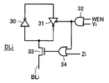
図4は、図3に示すデータラッチDL0−DLmの構成の一例を示す図である。図4において、データラッチDLi(I=0−m)は、インバータ30と、トライステートインバータ31とを含む。トライステートインバータ31は、書込活性化信号WENと列選択信号Yiを受けるゲート回路32の出力信号に従って選択的に活性化される。トライステートインバータ31は、ゲート回路32の出力信号がHレベルのとき非活性状態とされ、出力ハイインピーダンス状態となる。トライステートインバータ31の活性化時、インバータ30およびトライステートインバータ31により、インバータラッチが構成される。
FIG. 4 is a diagram showing an example of the configuration of data latches DL0 to DLm shown in FIG. In FIG. 4, data latch DLi (I = 0-m) includes an
データラッチDLiは、さらに、ラッチ指示信号LATに従ってトライステートインバータ31の出力を対応のビット線BLiに結合するトランスファーゲート33を含む。
Data latch DLi further includes a
データ書込時、この書込活性化信号WENが活性状態とされ、また、ラッチ指示信号LATも活性状態とされる。応じて、トランスファーゲート33が導通し、インバータ30の入力が対応のビット線BLiに接続される。対応のビット線BLiに列選択ゲート(CSGi)を介して書込データが伝達されるとき、列選択信号Yiは選択状態のHレベルである。したがって、この状態においては、ゲート回路32の出力信号がHレベルとなり、トライステートインバータ31が出力ハイインピーダンス状態となる。ビット線BLiへの書込データの伝達が完了すると、列選択信号Yiが非活性状態となり、応じて、トライステートインバータ31が活性化され、ビット線を介して伝達された書込データをラッチする。
At the time of data writing, write activation signal WEN is activated, and latch instruction signal LAT is also activated. Accordingly,
データ書込時に、まず、たとえばページモードに従って、図3に示す列選択信号Y0−Ymが順次選択状態へ駆動され、対応のデータラッチDL0−DLmに、書込データがラッチされる。 At the time of data writing, first, column selection signals Y0-Ym shown in FIG. 3, for example, are sequentially driven to a selected state in accordance with the page mode, for example, and write data is latched in corresponding data latches DL0-DLm.
図5は、図3および図4に示す不揮発性半導体記憶装置のデータ書込時の動作を示すフロー図である。以下、図5に示すフロー図を参照して、図3および図4に示す不揮発性半導体記憶装置のデータ書込時の動作について説明する。 FIG. 5 is a flowchart showing an operation at the time of data writing of the nonvolatile semiconductor memory device shown in FIGS. Hereinafter, with reference to the flowchart shown in FIG. 5, the operation at the time of data writing of the nonvolatile semiconductor memory device shown in FIGS. 3 and 4 will be described.
まず、この不揮発性半導体記憶装置において、外部からのコマンドによりデータ書込が指定されたかの判定が行なわれる(ステップSP1)。この書込指示は、外部からのコマンドCMDを図2に示す制御回路24でデコードすることにより判定される。データ書込指示が与えられるまで、書込動作は待ち合わせられる。
First, in this nonvolatile semiconductor memory device, it is determined whether data writing is designated by an external command (step SP1). This write instruction is determined by decoding an external command CMD by the
データ書込指示が与えられると、先ず、書込アドレスに従って選択メモリセルを含むブロックまたはワード線(コントロールゲート線およびメモリゲート線)が選択される。この選択ブロックまたは選択行のメモリセルの消去が行われる(ステップSP2)。ここで、消去が、ブロック単位の場合、この選択ブロックにおいて各メモリセル行の消去が、順次実行される(ステップSP3)。この消去時に、データラッチ回路20のデータラッチを用いて、消去ベリファイが実行されても良い。消去完了のメモリセルに対しては、対応のデータラッチを消去完了データをラッチする状態に設定する(消去時に消去阻止電圧がビット線に伝達される)。
When a data write instruction is given, a block or word line (control gate line and memory gate line) including a selected memory cell is first selected according to a write address. The memory cells in the selected block or selected row are erased (step SP2). Here, when erasing is in units of blocks, each memory cell row is sequentially erased in this selected block (step SP3). At the time of erasing, erase verify may be executed using the data latch of the
消去対象のメモリセルの消去が完了すると、次いで、書込データの転送およびデータラッチ(DL)での書込データのラッチが行われる(ステップSP4)。この場合、例えばページモードでビット線が順次選択されて書込データの転送および書込データのラッチが行われる。ここでページ書込について一例として説明すると、先頭アドレスと先頭書込データが与えられる。次いで、この先頭アドレスを列選択回路18においてデコードし、対応の列選択ゲートCG(CG0−CGmのいずれか)を導通させ、データの書込を行なう。このとき、図4に示すラッチ指示信号LATはHレベルの活性状態であり、データラッチDL(DL0−DLm)は、すべて対応のビット線上のデータを取込む状態に設定される。列選択信号Yiが選択状態へ駆動されると、対応のビット線データの取込およびラッチが行なわれる。次いで、この先頭アドレスから、図示しないカウント回路がカウント動作を開始し、列選択信号を順次更新して、連続して与えられるデータが順次書込まれてラッチされる。
When the erasure of the memory cell to be erased is completed, the write data is transferred and the write data is latched in the data latch (DL) (step SP4). In this case, for example, the bit lines are sequentially selected in the page mode, and write data is transferred and write data is latched. Here, when page writing is described as an example, a head address and head write data are given. Next, the head address is decoded by the
1行のメモリセル(コントロールゲート線およびメモリゲート線に接続されるメモリセル)に対する書込データの転送およびラッチが完了するまで、この書込データの転送およびラッチが行われる(ステップSP5)。これにより、1行(1ページ)の書込データのラッチが完了する。 The write data is transferred and latched until transfer and latch of the write data to one row of memory cells (control gate line and memory cells connected to the memory gate line) are completed (step SP5). Thereby, the latch of the write data of one row (one page) is completed.
全書込データの書込が完了すると、一旦、ラッチ指示信号LATが非活性状態とされ、データラッチDLと対応のビット線BLとが分離される。この状態で、次いで、書込に必要な電圧を、図2に示す内部電圧発生回路26により設定する。この状態で、データラッチDLと対応のビット線BLとを、再びラッチ指示信号LATを活性化して接続する(ステップSP6)。これにより、各ビット線BL0−BLmには、書込データが伝達される。この場合、メモリセルが書込まれない場合には、対応のビット線は、1.5V程度の電圧レベルに設定され、書込を行なうビット線には、電圧0.8Vが伝達される。
When the writing of all the write data is completed, the latch instruction signal LAT is once inactivated, and the data latch DL and the corresponding bit line BL are separated. In this state, the voltage required for writing is then set by internal
一例として、データ“0”が、メモリセルトランジスタのしきい値電圧が高い状態、すなわち書込状態に対応し、データ“1”がメモリセルトランジスタのしきい値電圧が低い状態、すなわち、消去状態に対応するとする。データ“1”が伝達されたビット線は、書込を行う必要があり、書込選択電圧の0.8Vに設定される。一方、データ“0”が伝達されたビット線は、書込を行う必要がなく、1.5Vの書込阻止電圧レベルに設定される。 As an example, data “0” corresponds to a state in which the threshold voltage of the memory cell transistor is high, that is, a write state, and data “1” is a state in which the threshold voltage of the memory cell transistor is low, that is, an erase state. Suppose that The bit line to which data “1” is transmitted needs to be written, and is set to a write selection voltage of 0.8V. On the other hand, the bit line to which data “0” has been transmitted does not need to be written, and is set to a write inhibition voltage level of 1.5V.
データ“0”および“1”が、それぞれ、LレベルおよびHレベルに対応するとすると、以下の構成を利用することにより、書込時、書込データに応じてビット線電圧を設定することができる。すなわち、データラッチDLにおいてインバータ30およびトライステートインバータ31の動作電源電圧Vdとして、ハイ側電圧Vdhを、1.5Vに設定し、ロー側電源電圧Vdlを、0.8Vに設定する。データ“0”が伝達されたビット線に対しては、データラッチによりLレベルの電圧、すなわちロー側電源電圧Vdlが伝達され、このビット線は書込選択電圧レベルに設定される。データ“1”が伝達されたビット線については、対応のデータラッチによりHレベル電圧、すなわちハイ側電源電圧Vdhが伝達され、このビット線は、書込阻止電圧レベルに設定される。これにより、書込データに応じた電圧レベルに対応のビット線電圧を設定して、選択的に書込を行なうことができる(書込が行なわれないメモリセルは、消去状態、すなわちデータ“1”の記憶状態に維持される)。
If data “0” and “1” correspond to the L level and the H level, respectively, the bit line voltage can be set according to the write data at the time of writing by using the following configuration. . That is, in the data latch DL, as the operation power supply voltage Vd of the
また、メモリゲート線選択駆動回路14に対しては、メモリゲート電圧Vmgとして、ハイ側電圧(選択電圧レベル)が11V、ロー側電圧(非選択電圧レベル)3.5Vが動作電源電圧として伝達される。これにより、選択行のメモリゲート線MGは、11V、非選択行のメモリゲート線MGは、3.5Vにそれぞれ設定される。
Further, to the memory gate line
コントロールゲート線選択駆動回路12へは、電圧Vcgのハイ側電圧(選択電圧レベル)Vcghとして1V、ロー側電圧(非選択電圧レベル)Vcglとして接地電圧が伝達される。従って、この状態においては、ビット線BL0−BLmには、並行して書込データに応じた電圧が伝達されて、データラッチによりラッチされる。
The control gate line
この状態で、図3に示すシフトレジスタ回路SFRの出力を順次選択状態に駆動する。応じて、、対応のソース線ドライバを介してソース線SL0−SLkへ順次、書込電圧(5V)が伝達される。これにより、ソース線単位で、データの書込が実行される(ステップSP7)。ビット線に書込電圧が伝達されても、非選択状態のソース線は、書込阻止電圧レベルである。従って、ソース線からビット線に対しては電流が流れるのは抑制され、選択行かつ非選択列のメモリセルの書込ディスターバンスが抑制される。 In this state, the output of the shift register circuit SFR shown in FIG. 3 is sequentially driven to the selected state. Accordingly, the write voltage (5 V) is sequentially transmitted to source lines SL0 to SLk through corresponding source line drivers. Thereby, data writing is executed in units of source lines (step SP7). Even if the write voltage is transmitted to the bit line, the unselected source line is at the write inhibit voltage level. Therefore, the flow of current from the source line to the bit line is suppressed, and the write disturbance of the memory cells in the selected row and non-selected column is suppressed.
このソース線単位のデータ書込が、すべてのソース線に対して行なわれたかの判定が行なわれる(ステップSP8)。この最終ソース線が選択状態へ駆動されたかの判定は、ソース線SLkが選択状態へ駆動されたかの判定またはシフトレジスタ回路SFRにおいて最終出力が選択状態に設定されているかの判定により行われる。 It is determined whether the data writing in units of source lines has been performed for all the source lines (step SP8). The determination as to whether or not the final source line has been driven to the selected state is made by determining whether or not the source line SLk has been driven to the selected state or determining whether or not the final output is set to the selected state in the shift register circuit SFR.
すべてのソース線に対する選択状態への駆動が完了すると、1行のメモリセルのデータの書込が完了する。次いで、全アドレスに対する書込が完了したかの判定が行われる(ステップSP9)。書込が完了していない場合には、同一ブロックの次のメモリセル行に対するデータの書込を行うために、再度、ステップSP4へ戻り、次の行のメモリセルに対するデータの転送およびラッチが行われる。書込ブロックにおいて、データの書込が全アドレスに対して完了するまで、この動作が繰返し実行される。書込ブロックの書込アドレスに対する書込が完了すると、データの書込が完了する。なお、書込/消去が、ブロック単位ではなく、ワード線単位で行われても良い。 When the driving of all the source lines to the selected state is completed, the writing of data in one row of memory cells is completed. Next, it is determined whether writing to all addresses is completed (step SP9). If the writing has not been completed, in order to write data to the next memory cell row of the same block, the process returns to step SP4 again, and data transfer and latch to the memory cell of the next row is performed. Is called. In the writing block, this operation is repeatedly executed until data writing is completed for all addresses. When the writing to the writing address of the writing block is completed, the data writing is completed. Note that writing / erasing may be performed not in units of blocks but in units of word lines.
すなわち、本実施の形態1においては、ソース線を全て選択状態に設定して、ビット線ごとにデータの書込を行なうのではなく、ソース線単位で、データの書込を行なう。ホットエレクトロンを用いたデータの書込の場合、消費電流が大きく、1行のメモリセルに対して同時に並行して書込を行う場合、消費電流が大きくなる可能性がある。しかしながら、ソース線単位でデータの書込を行なっており、データ書込時の消費電流増大は十分に抑制される。また、ソース線選択駆動回路は、ソース線単位で書込電流を供給するだけでよい。従って、ソース線の負荷が大きい場合においても、安定に書込電圧を高速で選択ソース線に伝達することができる。 That is, in the first embodiment, not all source lines are set to a selected state and data is written for each bit line, but data is written in units of source lines. In the case of writing data using hot electrons, the current consumption is large, and in the case where data is written in parallel to one row of memory cells, the current consumption may increase. However, since data is written in units of source lines, an increase in current consumption during data writing is sufficiently suppressed. Further, the source line selection drive circuit need only supply the write current in units of source lines. Therefore, even when the load on the source line is large, the write voltage can be stably transmitted to the selected source line at high speed.
ビット線が並行して書込選択状態に駆動される。しかしながら、ビット線は、上層のメタル配線で構成され、その負荷はソース線に比べて小さい。従って、ビット線BL0−BLmを並行して書込データに応じて書込選択電圧レベルに駆動しても、安定にビット線書込電圧を供給することができる。また、非選択状態のソース線に対応して配置されるビット線は、単に書込データに応じて書込選択電圧または書込阻止電圧レベルにプリチャージされることが要求されるだけである。従って、ビット線に並行に書込データを伝達しても、その消費電流の増大は充分に抑制される。 The bit lines are driven to the write selection state in parallel. However, the bit line is composed of an upper layer metal wiring, and its load is smaller than that of the source line. Therefore, even if the bit lines BL0 to BLm are driven in parallel to the write selection voltage level according to the write data, the bit line write voltage can be stably supplied. Further, the bit line arranged corresponding to the unselected source line is merely required to be precharged to the write selection voltage or write inhibition voltage level according to the write data. Therefore, even if write data is transmitted in parallel to the bit line, an increase in current consumption is sufficiently suppressed.
図6は、この図3に示す不揮発性半導体記憶装置のデータ書込時のビット線、ソース線およびラッチ指示信号の信号波形を示す図である。書込時において、選択行のコントロールゲート線CGおよびメモリゲート線MGは、選択電圧レベルに維持される。 FIG. 6 is a diagram showing signal waveforms of the bit line, source line and latch instruction signal at the time of data writing in the nonvolatile semiconductor memory device shown in FIG. At the time of writing, control gate line CG and memory gate line MG in the selected row are maintained at the selected voltage level.
時刻t0以前の書込開始前においては、ビット線BL0−BLmが、書込阻止電圧レベルにプリチャージされる状態を示す。書込開始前においては、各ビット線は、接地電圧レベルにプリチャージされてもよく、また、書込選択電圧レベルにプリチャージされてもよい。 Prior to the start of writing before time t0, bit lines BL0-BLm are precharged to the write inhibition voltage level. Prior to the start of writing, each bit line may be precharged to the ground voltage level or precharged to the write selection voltage level.
時刻t0において、データの書込が開始される(図5のステップSP6、SP7)。これにより、データラッチDLと対応のビット線BLとが接続され、各ビット線には書込データが伝達される。ここで、図6においては、説明を簡略化するために、ビット線BL0−BLm全てに、書込を行なうデータが伝達された場合を一例として示す。書込データに応じて、ビット線BL0−BLm各々の電圧レベルは0.8Vおよび1.5Vのいずれかに設定される。 At time t0, data writing is started (steps SP6 and SP7 in FIG. 5). Thus, data latch DL and corresponding bit line BL are connected, and write data is transmitted to each bit line. Here, FIG. 6 shows, as an example, a case where data to be written is transmitted to all bit lines BL0 to BLm for the sake of simplicity. Depending on the write data, the voltage level of each of bit lines BL0-BLm is set to either 0.8V or 1.5V.
時刻t1において、ビット線の電圧レベルが、書込データに応じて設定されると、次いで、時刻t2から、ソース線SL0−SLkが、順次、所定期間活性状態に維持される。これにより、各ソース線において、ソース線SLとビット線BLとの間の電圧に従って電流が流れ、ホットエレクトロンによる電荷蓄積膜への電子の注入が実行される。 When the voltage level of the bit line is set according to the write data at time t1, source lines SL0 to SLk are successively maintained in an active state for a predetermined period from time t2. Thereby, in each source line, a current flows in accordance with the voltage between the source line SL and the bit line BL, and electrons are injected into the charge storage film by hot electrons.
時刻t3において、最終のソース線SLkに接続されるメモリセルへのデータの書込が完了する。この書込完了後、時刻t4においてラッチ指示信号LATを非活性状態に駆動する。この場合、例えば、ビット線BL0−BLmは、図示しないプリチャージ回路により所定電圧レベルにプリチャージされる。図6においては、書込完了後のビット線プリチャージ電圧が、書込阻止電圧レベルの場合を一例として示す。しかしながら、このビット線プリチャージ電圧は、接地電圧レベルであっても良く、また、書込選択電圧レベルであってもよい(ビット線プリチャージ回路により所望のプリチャージ電圧レベルに設定する)。これにより、1行のメモリセルに対する書込が完了する。 At time t3, data writing to the memory cell connected to the final source line SLk is completed. After completion of the writing, the latch instruction signal LAT is driven to an inactive state at time t4. In this case, for example, the bit lines BL0 to BLm are precharged to a predetermined voltage level by a precharge circuit (not shown). FIG. 6 shows, as an example, the case where the bit line precharge voltage after completion of writing is at the write inhibition voltage level. However, the bit line precharge voltage may be a ground voltage level or a write selection voltage level (set to a desired precharge voltage level by the bit line precharge circuit). This completes the writing to one row of memory cells.
書込時においても、このデータラッチ回路にラッチされた書込データとメモリセルのデータとを比較し、書込が正確に行なわれたかのベリファイ動作が行なわれる。このベリファイ結果に従って、書込が完了したメモリセルに対するラッチデータは、書込阻止電圧に対応するデータに設定される。 Even at the time of writing, the write data latched in the data latch circuit is compared with the data in the memory cell, and a verify operation is performed to determine whether the writing has been performed correctly. According to the verify result, the latch data for the memory cell for which writing has been completed is set to data corresponding to the write inhibition voltage.
図7は、データ書込時における各メモリセルに対する印加電圧を示す図である。図7においては、2行4列に配列されるメモリセルMC00−MC03およびMC10−MC13を代表的に示す。選択行のメモリゲート線MG0は11Vの選択状態に設定され、非選択行のメモリゲート線MG1は、3.5Vの非選択状態に設定される。選択行のコントロールゲート線CG0が、1Vの選択状態に設定され、非選択行のコントロールゲート線CG1は0Vの非選択状態に設定される。ソース線SL0が書込選択状態の5Vに設定され、ソース線SL1は、非選択状態の1.5Vに設定される。ビット線BL0−BL3は、それぞれデータ書込を行なうため、0.8Vの書込選択状態に設定される。 FIG. 7 shows a voltage applied to each memory cell during data writing. FIG. 7 representatively shows memory cells MC00-MC03 and MC10-MC13 arranged in 2 rows and 4 columns. The memory gate line MG0 in the selected row is set to the 11V selected state, and the memory gate line MG1 in the unselected row is set to the 3.5V unselected state. The control gate line CG0 of the selected row is set to the 1V selected state, and the control gate line CG1 of the unselected row is set to the 0V unselected state. Source line SL0 is set to 5V in the write selected state, and source line SL1 is set to 1.5V in the non-selected state. Bit lines BL0 to BL3 are set to a write selection state of 0.8 V in order to perform data writing.
この条件下においては、メモリセルMC00およびMC01において、ソース線SL0に接続される不純物領域2bからビット線BL0に接続される不純物領域2aに電流が流れる。コントロールゲート線CG0が1Vであり、選択トランジスタSTのチャネル領域において弱い反転層が形成され、メモリセルトランジスタMTの電荷蓄積膜へホットエレクトロンの注入が行なわれる。メモリセルMC01についても同様である。
Under this condition, in memory cells MC00 and MC01, a current flows from
メモリセルMC00およびMC01が、消去状態に維持すべきメモリセルであるとする。この場合、ビット線BL0およびBL1は、書込阻止電圧レベルに設定される。このディスターバンスを、いま、Aモードと称す。このAモードディスターバンスにおいては、ソース線SLとビット線BLとの電圧差が大きく、リーク電流が流れ、ホットエレクトロンによる弱い書込が行なわれる可能性がある。しかしながら、対応のソース線SL0が、選択状態に維持される期間は、短く、単に対応の列のメモリセルに書込が行われる期間である。1行のメモリセルに対して順次書込が行われる際に、全ソース線を選択状態に維持して、ビット線に順次書込データを転送する構成の場合に比べて、Aモードディスターバンスを受ける期間を大幅に短縮することができ、書込データの信頼性およびデータ保持特性の劣化を抑制することができる。 Assume that memory cells MC00 and MC01 are memory cells to be maintained in the erased state. In this case, bit lines BL0 and BL1 are set to the write inhibition voltage level. This disturbance is now called A mode. In this A mode disturbance, the voltage difference between the source line SL and the bit line BL is large, a leak current flows, and there is a possibility that weak writing by hot electrons is performed. However, the period during which the corresponding source line SL0 is maintained in the selected state is short, and is simply a period in which writing is performed in the memory cells in the corresponding column. Compared with the configuration in which all the source lines are maintained in the selected state and the write data is sequentially transferred to the bit lines when sequential writing is performed on the memory cells in one row, the A mode disturbance is achieved. The period during which the data is received can be greatly shortened, and the deterioration of the reliability of the write data and the data retention characteristics can be suppressed.
メモリセルMC02およびMC03においては、ソース線SL1は、1.5Vであり、選択トランジスタSTを介してビット線BL2およびBL3それぞれへ、ソース線SL1から電流が流れる。このディスターバンスモードを、いま、Iモードと称す。このIモードディスターバンスにおいては、メモリセルMC02およびMC03は、選択トランジスタSTが弱いオン状態であり、流れる電流量は小さい。従って、ホットエレクトロンの発生による弱い書込が生じても、これらのメモリセルMC02およびMC03は、書込対象のメモリセルである。従って誤書込の問題は生じない。 In memory cells MC02 and MC03, source line SL1 is 1.5 V, and current flows from source line SL1 to bit lines BL2 and BL3 via select transistor ST. This disturbance mode is now called the I mode. In this I-mode disturbance, the memory cells MC02 and MC03 are in the on state where the select transistor ST is weak, and the amount of current flowing is small. Therefore, even if weak writing occurs due to generation of hot electrons, these memory cells MC02 and MC03 are memory cells to be written. Therefore, the problem of erroneous writing does not occur.
メモリセルMC02およびMC03が、非書込対象のメモリセルの場合、ビット線BL2およびBL3には、書込阻止電圧が伝達される。この書込阻止電圧は、非選択状態のソース線の電圧と同一電圧レベルである。従って、ソース線の非選択状態においては、メモリセルを介して電流は流れない。ソース線SL1の選択時においても、選択トランジスタSTのコントロールゲートとビット線とが逆バイアス状態であり、選択トランジスタSTは、オフ状態である。従って、消去状態に維持すべきメモリセルの誤書込は回避される。 When memory cells MC02 and MC03 are non-write target memory cells, a write inhibition voltage is transmitted to bit lines BL2 and BL3. This write inhibition voltage is at the same voltage level as the voltage of the unselected source line. Therefore, no current flows through the memory cell when the source line is not selected. Even when the source line SL1 is selected, the control gate and the bit line of the selection transistor ST are in the reverse bias state, and the selection transistor ST is in the off state. Accordingly, erroneous writing of the memory cell to be maintained in the erased state is avoided.
メモリセルMC10およびMC11は、ビット線BL0およびBL1に接続される不純物領域2aが選択状態の0.8Vであり、ソース線SL0に接続される不純物領域2aが、5Vである。この非選択のメモリセルMC10およびMC11のディスターバンスを、Gモードと称す。このGモードのディスターバンスにおいては、選択トランジスタSTは、コントロールゲートとソースとが逆バイアス状態であり、深いオフ状態である。従って、メモリセルMC10およびMC11において、ソース線SL0からビット線BL0およびBL1へ流れる電流は、ほぼ無視することのできる電流量である。また、メモリセルゲート線MG1が3.5Vであり、不純物領域2bから電荷蓄積膜へのトンネル電流による誤書込のディスターバンスが生じる可能性は、ほぼ無視することができる。
In memory cells MC10 and MC11,
メモリセルMC12およびMC13においては、ビット線BL2およびBL3に接続される不純物領域2aが0.8Vであり、ソース線SL1に接続される不純物領域2bは、1.5Vである。コントロールゲート線CG1が0Vであり、選択トランジスタは深いオフ状態である。この状態のディスターバンスを、Dモードと称す。このDモードディスターバンスにおいても、メモリセルゲートと不純物領域2bの間でのトンネル電流による電荷蓄積膜への電子注入が生じる可能性があるものの、この可能性は十分に小さく、ほぼ無視することができる。
In memory cells MC12 and MC13,
以上のように、この発明の実施の形態1に従えば、以下の効果を得ることができる。最もディスターバンスの影響の大きなAモードのディスターバンスを十分に抑制することができ、保持データの信頼性を保証することができる。また、ソース線単位でデータの書込を行なっており、全ソース線を選択状態に維持した状態でビット線単位でデータの書込を行なっていない。従って、ソース線選択駆動回路は、1本のソース線を駆動することが要求されるだけである。従って、記憶容量が増大して1行のメモリセルの数が増大しても、ソース線選択駆動回路が要求される電流駆動力は、増大せず、その回路の占有面積の増大を抑制することができる。また、安定にソース線に書込電圧を高速で伝達することができ、高速かつ安定にデータの書込を行うことができる。 As described above, according to the first embodiment of the present invention, the following effects can be obtained. It is possible to sufficiently suppress the disturbance of the A mode, which has the greatest influence of disturbance, and to guarantee the reliability of retained data. Further, data is written in units of source lines, and data is not written in units of bit lines while all source lines are kept in a selected state. Therefore, the source line selection drive circuit is only required to drive one source line. Therefore, even if the storage capacity increases and the number of memory cells in one row increases, the current driving force required for the source line selection driving circuit does not increase, and the increase in the area occupied by the circuit is suppressed. Can do. In addition, the write voltage can be stably transmitted to the source line at high speed, and data can be written stably at high speed.
また、非選択メモリセルがディスターバンスを受ける時間を短縮することができ、書込時のディスターバンスによる誤書込を防止することができる。また、ソース線には複数列のメモリセルが接続されるため、複数列のメモリセルに対し並行してデータの書込を行なうことができ、書込に要する時間を、ビット線毎にデータを書込む構成に比べて、短縮することができる。 In addition, it is possible to shorten the time during which the non-selected memory cells are subjected to disturbance, and to prevent erroneous writing due to disturbance during writing. In addition, since a plurality of columns of memory cells are connected to the source line, data can be written in parallel to the plurality of columns of memory cells, and the time required for writing can be reduced for each bit line. Compared to the writing configuration, it can be shortened.
[実施の形態2]
図8は、この発明の実施の形態2に従う不揮発性半導体記憶装置のデータ書込時の動作を示すタイミング図である。この発明の実施の形態2における不揮発性半導体記憶装置の全体の構成は、先の図2に示す不揮発性半導体記憶装置の構成と同様である。また、図8においても、選択行のメモリセルに対しては、全て書込状態に設定する動作が、一例として示される。
[Embodiment 2]
FIG. 8 is a timing diagram representing an operation at the time of data writing of the nonvolatile semiconductor memory device according to the second embodiment of the present invention. The entire configuration of the nonvolatile semiconductor memory device according to the second embodiment of the present invention is the same as that of the nonvolatile semiconductor memory device shown in FIG. Also, in FIG. 8, the operation of setting all the memory cells in the selected row to the write state is shown as an example.
この実施の形態2においては、図8に示すように、ソース線SL0−SLkは、実施の形態1と同様、順次選択状態に駆動される。実施の形態2においては、書込時に、各選択状態とされるソース線に対応して設けられるビット線を、順次選択状態へ書込データに応じて駆動する。ビット線は、非選択時、書込阻止電圧レベルに維持される。したがって、ソース線SL0が選択状態に設定された場合、対応して配置されるビット線BL0およびBL1が順次選択状態へ駆動される。同様、ソース線SL1が選択状態へ駆動された場合、対応のビット線BL2およびBL3が、順次書込データに応じて選択状態に駆動される。したがって、ソース線単位で、ソース線が順次選択状態へ駆動されても、各ビット線に書込データに応じて書込電圧を伝達しており、書込は、ビット線単位である。したがって、書込時、ホットエレクトロン注入時においても、消費電流を低減でき、安定にソース線SLに書込電圧および書込電流を伝達することができる。 In the second embodiment, as shown in FIG. 8, source lines SL0 to SLk are sequentially driven to a selected state as in the first embodiment. In the second embodiment, at the time of writing, the bit lines provided corresponding to the source lines in each selected state are sequentially driven to the selected state according to the write data. The bit line is maintained at the write inhibit voltage level when not selected. Therefore, when source line SL0 is set to the selected state, bit lines BL0 and BL1 arranged correspondingly are sequentially driven to the selected state. Similarly, when source line SL1 is driven to a selected state, corresponding bit lines BL2 and BL3 are sequentially driven to a selected state according to write data. Therefore, even if the source lines are sequentially driven to the selected state in units of source lines, the write voltage is transmitted to each bit line according to the write data, and writing is performed in units of bit lines. Therefore, current consumption can be reduced during writing and hot electron injection, and the writing voltage and writing current can be stably transmitted to the source line SL.
また、2列のメモリセルに並行して書込電流を供給する必要がなく、1列のメモリセルに対して書込電流を供給するだけである。従って、選択メモリセルに対して、大きな電流を供給することができる。従って、ソース高電界によるホットエレクトロンの発生効率を高くすることができ、書込に要する時間を短縮することができる。この実施の形態2におけるソース線の選択期間は、選択メモリセルの書込に要する時間に応じて適切に定められる。実施の形態1および2において、ソース線が選択状態に維持される期間が同じであることは、特に要求されない。
Further, it is not necessary to supply the write current in parallel to the two columns of memory cells, and only the write current is supplied to the one column of memory cells. Therefore, a large current can be supplied to the selected memory cell. Therefore, the generation efficiency of hot electrons due to the high source electric field can be increased, and the time required for writing can be shortened. The source line selection period in the second embodiment is appropriately determined according to the time required for writing the selected memory cell. In
図9は、この発明の実施の形態2に従う不揮発性半導体記憶装置のデータ書込時のメモリセルへの印加電圧を示す図である。図9においても、2行4列に配列されるメモリセルを代表的に示す。図9において、選択行のメモリゲート線MG0が11Vに設定され、非選択行のメモリゲート線MG1が、3.5Vに設定される。選択行のコントロールゲート線CG0が1Vに設定され、非選択行のコントロールゲート線CG1が0Vに設定される。選択列のビット線BL0が書込選択状態の0.8Vに設定され、非選択列のビット線BL1−BL3が、非選択状態の1.5Vに設定される。選択ソース線SL0が、5Vに設定され、非選択ソース線SL1が1.5Vに設定される。 FIG. 9 shows a voltage applied to the memory cell at the time of data writing in the nonvolatile semiconductor memory device according to the second embodiment of the present invention. FIG. 9 also representatively shows memory cells arranged in 2 rows and 4 columns. In FIG. 9, the memory gate line MG0 of the selected row is set to 11V, and the memory gate line MG1 of the non-selected row is set to 3.5V. The control gate line CG0 of the selected row is set to 1V, and the control gate line CG1 of the non-selected row is set to 0V. The bit line BL0 in the selected column is set to 0.8V in the write selected state, and the bit lines BL1 to BL3 in the unselected column are set to 1.5V in the non-selected state. The selected source line SL0 is set to 5V, and the unselected source line SL1 is set to 1.5V.
この条件下においては、メモリセルMC00に対して、データの書込が実行される。メモリセルMC01は、メモリセルトランジスタMTのメモリゲートおよび不純物領域2bが選択状態とされ、また、選択トランジスタSTは、コントロールゲートが選択状態の電圧レベルであり、不純物領域2aが非選択状態である。したがって、メモリセルMC01においてディスターバンスとして、Aモードのディスターバンスが生じる。しかしながら、メモリセルMC01が、Aモードのディスターバンスを受ける期間は、対応のソース線SL0が選択状態に維持される期間よりも充分に短い。従って、メモリセルMC01のAモードのディスターバンスを受ける時間を十分に短くすることができ、その影響は充分に抑制することができる。
Under this condition, data is written to the memory cell MC00. In the memory cell MC01, the memory gate of the memory cell transistor MT and the
メモリセルMC02およびMC03は、ビット線およびソース線が同一電圧レベルであり、チャネル電流は流れない。従って、ディスターバンスは十分に抑制することができる。選択行において、ディスターバンスモードとして、Aモードを受けるメモリセルMC01が存在するものの、その数は、全ソース線を並行して選択状態に駆動する場合に比べて低減することができ、また、個々のメモリセルがAモードのディスターバンスを受ける時間を短縮することができる。 In memory cells MC02 and MC03, the bit line and the source line are at the same voltage level, and no channel current flows. Therefore, disturbance can be sufficiently suppressed. In the selected row, although there are memory cells MC01 that receive the A mode as the disturbance mode, the number thereof can be reduced as compared with the case where all the source lines are driven to the selected state in parallel. The time for each memory cell to receive the A mode disturbance can be shortened.
なお、メモリセルMC10は、Gモードのディスターバンスを受けるものの、ビット線BL0に書込電圧が伝達される時間は、上述のように短くすることができ、その影響は、充分に抑制することができる。 Although memory cell MC10 receives G-mode disturbance, the time for which the write voltage is transmitted to bit line BL0 can be shortened as described above, and the influence thereof can be sufficiently suppressed. Can do.
メモリセルMC11は、Fモードのディスターバンスを受ける。このFモードのディスターバンスでは、選択トランジスタSTのコントロールゲートおよびソース(ビット線)が逆バイアス状態であり、充分に深いオフ状態となり、ソース線SL0からビット線BL0へのリーク電流は十分に抑制することができる。また、メモリセルトランジスタMTのメモリゲートの電圧は低い電圧レベルであり、ホットエレクトロン/ホットホールの影響は十分小さくすることができる。 Memory cell MC11 receives F-mode disturbance. In this F-mode disturbance, the control gate and source (bit line) of the selection transistor ST are in a reverse bias state, and are sufficiently deep off, and the leakage current from the source line SL0 to the bit line BL0 is sufficiently suppressed. can do. Further, the voltage of the memory gate of the memory cell transistor MT is at a low voltage level, and the influence of hot electrons / hot holes can be sufficiently reduced.
メモリセルMC12およびMC13は、ビット線およびソース線の電圧レベルが同一電圧レベルである。したがって、リーク電流は流れず、ディスターバンスは充分に抑制することができる。 In memory cells MC12 and MC13, the voltage levels of the bit line and the source line are the same voltage level. Therefore, no leak current flows and disturbance can be sufficiently suppressed.
図10は、この発明の実施の形態2に従う不揮発性半導体記憶装置の要部の構成を概略的に示す図である。この図10に示す構成においては、ビット線BL0−BLmに対して設けられるデータラッチDL0−DLmは、ビット線シフト回路40の出力信号Z0−Zmに従ってデータラッチ/転送動作が制御される。このビット線シフト回路40は、シフトクロック信号SCLKを分周する分周回路42の出力する分周クロック信号DCLKに従ってシフト動作を行ない、その出力信号Z0−Zmを順次選択状態へ駆動する。
FIG. 10 schematically shows a structure of a main portion of the nonvolatile semiconductor memory device according to the second embodiment of the present invention. In the configuration shown in FIG. 10, data latch / transfer operations of data latches DL0-DLm provided for bit lines BL0-BLm are controlled according to output signals Z0-Zm of bit
シフトクロック信号CLKは、図2に示す制御回路24から、データ書込時生成され、シフトレジスタ回路SFRが、このシフトクロック信号SCLKに従ってシフト動作を行なう。ソース線選択駆動回路16の構成は、図3に示すソース線選択駆動回路16の構成と同じであり、対応する部分には、同一参照符号を付し、その詳細説明は省略する。ただし、ソース線が選択状態に維持される期間が、実施の形態1および2の間で異なる場合には、シフトクロック信号SCLKの周期を変更する。
Shift clock signal CLK is generated at the time of data writing from
図11は、図10に示すデータラッチDL0−DLmの構成の一例を示す図である。図11においては、ビット線BLiに対して設けられるデータラッチDLiの構成を代表的に示す。この図11に示すデータラッチDLiの構成は、図4に示すデータラッチDLiと以下の点で、その構成が異なる。すなわち、ビット線BLiとの接続を制御するトランスファーゲート33へは、ゲート回路32の出力信号とビット線シフト回路40からの出力信号Ziを受けるOR回路34の出力信号が、ラッチ指示信号LATに代えて与えられる。この図11に示すデータラッチDLiの他の構成は、図4に示すデータラッチの構成と同じであり、対応する部分には同一参照番号を付し、その詳細説明は省略する。
FIG. 11 shows an example of the configuration of data latches DL0 to DLm shown in FIG. FIG. 11 representatively shows a configuration of data latch DLi provided for bit line BLi. The configuration of the data latch DLi shown in FIG. 11 is different from that of the data latch DLi shown in FIG. 4 in the following points. That is, to the
この図11に示すデータラッチDLiの場合、ビット線BLiに伝達された書込データは、列選択信号Yiに従ってインバータ30およびトライステートインバータ31によりラッチされる。ラッチ動作は、実施の形態1と同様である。
In the case of data latch DLi shown in FIG. 11, write data transmitted to bit line BLi is latched by
データ書込時、列選択信号Yiは非選択状態であり、ゲート回路32の出力信号はLレベルである。応じて、トライステートインバ−タ31がインバータとして動作し、書込データをラッチした状態を維持する。ビット線シフト回路40(図10参照)からの出力信号Ziに従って、トランスファーゲート33が順次導通状態へ駆動される。ビット線シフト回路40へ与えられる分周クロック信号DCLKは、分周回路42により、一例としてシフトクロック信号SCLKを2分周しており、その周期は、シフトクロック信号SCLKの1/2倍である。したがって、ビット線シフト回路40のシフトサイクルは、シフトレジスタ回路SFRのシフトサイクルの1/2倍となり、ソース線SLの選択時、対応のビット線を順次選択状態へ駆動することができる。
At the time of data writing, column selection signal Yi is in a non-selected state, and the output signal of
このOR回路34の出力信号に従って、図示しないビット線プリチャージ回路を介して対応のビット線を書込阻止電圧レベルに駆動することにより、書込完了後のビット線を書込阻止電圧レベルに維持することができる。このビット線プリチャージ回路は、一例として、OR回路34の出力信号をゲートに受けるPチャネルMOSトランジスタを利用することにより構成することができる。トランスファーゲート33の非導通時、このプリチャージMOSトランジスタにより、対応のビット線を書込阻止電圧レベルにプリチャージする。
In accordance with the output signal of
以上のように、本実施の形態2においては、ソース線単位でソース線を選択状態に駆動する構成において、さらに、各ビット線単位で、データの書込を行なっている。従って、書込時の消費電流を低減することができる。また、ソース線を駆動する回路の書込時の消費電流を低減でき、応じて回路規模を低減することができる。また、安定に書込ソース線電流を供給することができ、安定にデータの書込を行うことができる。 As described above, in the second embodiment, in the configuration in which the source line is driven to the selected state in units of source lines, data is written in units of bit lines. Therefore, current consumption during writing can be reduced. In addition, current consumption during writing of the circuit for driving the source line can be reduced, and the circuit scale can be reduced accordingly. Further, the write source line current can be stably supplied, and data can be stably written.
[変更例]
図12は、この発明の実施の形態2に従う不揮発性半導体記憶装置の変更例の要部の構成を概略的に示す図である。図12においては、列選択およびデータ書込/読出に関連する部分の構成を示す。メモリゲート線選択駆動回路およびコントロールゲート線選択駆動回路は、図面を簡略化するために示していない。この実施の形態3においても、不揮発性半導体記憶装置の全体の構成は、図2に示す不揮発性半導体記憶装置の全体の構成と同様である。
[Example of change]
FIG. 12 schematically shows a structure of a main portion of a modification of the nonvolatile semiconductor memory device according to the second embodiment of the present invention. FIG. 12 shows a configuration of a portion related to column selection and data writing / reading. The memory gate line selection drive circuit and the control gate line selection drive circuit are not shown in order to simplify the drawing. Also in the third embodiment, the entire configuration of the nonvolatile semiconductor memory device is the same as the entire configuration of the nonvolatile semiconductor memory device shown in FIG.
図12において、不揮発性半導体記憶装置は、入出力回路22からの書込データを順次格納する書込データレジスタ50を含む。この書込データレジスタ50は、書込活性化信号WENの活性化時、ゲート回路51から与えられるクロック信号に従って順次書込データを取込みラッチし、順次、ラッチデータを内部データ線IOL上に出力する。
12, the nonvolatile semiconductor memory device includes a
ゲート回路51は、分周クロック信号DCLKと書込クロック信号WCLKを受けるOR回路で構成され、クロック信号DCLKまたはWCLKに従って書込シフトクロック信号を生成して、書込データレジスタ50へ与える。
この不揮発性半導体記憶装置は、図2に示す列選択駆動回路18として、列デコーダ52と、シフトレジスタ54と、ゲート回路56と、Yゲート回路57とを含む。列デコーダ52は、書込活性化信号WENの非活性化時、与えられた列アドレス信号(図示せず)をデコードし、列選択信号を生成する。シフトレジスタ54は、書込活性化信号WENの活性化時、分周回路58からの分周クロック信号DCLKに従ってシフト動作を行なう。分周回路58は、シフトクロック信号SCLKを2分周して、分周クロック信号DCLKを生成する。
This nonvolatile semiconductor memory device includes a
ゲート回路56は、OR回路で構成され、シフトレジスタ54および列デコーダ52の出力信号の論理和を取った信号を出力する。このゲート回路56は、列デコーダ52の各出力信号とシフトレジスタ54との論理和を取って、Yゲート回路57に含まれる列選択ゲートそれぞれに対する列選択信号Y0−Ymを生成する。
Yゲート回路57においては、メモリセルアレイ10に含まれるビット線それぞれに対して列選択ゲート(CSG0−CSGm)が設けられる。これらの列選択ゲート(CSG0−CSGm)が、OR回路56から列選択ゲートそれぞれへ与えられる列選択信号に従って選択的に導通して、内部データ線IOLを選択列のビット線に結合する。
In
ソース線選択駆動回路16は、実施の形態1または2の構成と同じであり、データ書込時、シフトクロック信号SCLKに従ってシフト動作を行なってソース線(図示せず)を選択状態へ駆動する。
Source line
内部データ線IOLには、データ読出時、読出データをラッチする読出データレジスタ60が、さらに、設けられる。読出データレジスタ60の出力ラッチデータが、データ読出時、入出力回路22を介して外部読出データとして出力される。この読出データレジスタ60のラッチデータが、書込ベリファイ動作時、書込データレジスタ50に格納されるデータとの一致/不一致を比較するために用いられてもよい。
The internal data line IOL is further provided with a read data register 60 that latches read data when data is read. The output latch data of read data register 60 is output as external read data via input /
この図12に示す不揮発性半導体記憶装置においては、データ書込時、書込データレジスタ50が、入出力回路22から与えられる書込データを、ゲート回路51からのクロック信号(書込クロック信号WCLK)に従って順次取込みラッチする。この書込データレジスタ50は、たとえばファーストイン・ファーストアウトで構成されればよい。
In the nonvolatile semiconductor memory device shown in FIG. 12, at the time of data writing, write data register 50 receives write data supplied from input /
データ書込時、シフトクロック信号SCLKに従ってソース線選択駆動回路16がソース線SL0−SLkを順次選択状態へ駆動する。このとき、分周クロック信号DCLKに従って、シフトレジスタ54がシフト動作を行ない、Yゲート回路57の列選択ゲート(CSG0−CSGm)が順次導通状態となり、ビット線BL0−BLmが、順次、内部データ線IOLに電気的に接続される。このとき、ゲート回路51が、また分周クロック信号DCLKに従ってシフトクロック信号を生成する。書込データレジスタ50に格納されるデータが、順次、このゲート回路51の出力するクロック信号に従って内部データ線IOL上に伝達される。したがって、書込データレジスタ50に格納されたデータが順次、Yゲート回路57を介してビット線BL0−BLm上に伝達される。
At the time of data writing, source line
分周回路58は、シフトクロック信号SCLKを2分周しており、この分周クロック信号DCLKの周期は、シフトクロック信号SCLKの2倍である。したがって、この図12に示す構成においても、ソース線SL0−SLkを順次選択状態へ駆動する場合、選択状態のソース線に対応するビット線を順次選択状態へ駆動することができる。この場合、ページモード動作用に設けられる書込データレジスタ50を利用して、順次データの書込を行なっている。従って、メモリセルアレイ10内において、データ書込用のデータレジスタを各ビット線毎に設ける必要がなく、メモリセルアレイのレイアウト面積が低減される。
The
この変更例におけるデータ書込時の動作波形は、図8に示すタイミング図と同じである。ソース線の選択サイクルが、シフトクロック信号SCLKに従って設定される。Yゲートの選択期間、すなわちビット線の選択期間が、分周クロック信号DCLKにより設定される。 The operation waveform at the time of data writing in this modified example is the same as the timing chart shown in FIG. A source line selection cycle is set in accordance with shift clock signal SCLK. The selection period of the Y gate, that is, the selection period of the bit line is set by the divided clock signal DCLK.
なお、データ読出時においては、列デコーダ52がデコード動作を行ない、Yゲート回路57が選択列のビット線を内部データ線IOLに選択的に結合し、読出データレジスタ60に読出データがラッチされる。
At the time of data reading,
以上のように、この発明の実施の形態2に従えば、ソース線を順次選択状態へ駆動するとともに、選択状態のソース線に対応するビット線を順次選択状態へ駆動している。したがって、データの書込は、ビット線単位で行なわれており、データ書込時のホットエレクトロン注入による消費電流を低減することができ、高速かつ安定にデータの書込を行なうことができる。また、内部電圧(書込電圧)を発生する回路において、ソース線単位でソース線を選択状態に駆動しており、ソース線電圧を発生する部分の消費電流が低減され、内部電圧発生回路の規模を低減することができる。 As described above, according to the second embodiment of the present invention, the source lines are sequentially driven to the selected state, and the bit lines corresponding to the selected source lines are sequentially driven to the selected state. Therefore, data writing is performed in units of bit lines, current consumption due to hot electron injection during data writing can be reduced, and data writing can be performed stably at high speed. Further, in the circuit for generating the internal voltage (write voltage), the source line is driven to the selected state in units of the source line, the current consumption of the portion generating the source line voltage is reduced, and the scale of the internal voltage generating circuit Can be reduced.
[実施の形態3]
図13は、この発明の実施の形態3に従う不揮発性半導体記憶装置のデータ書込時の動作を示すタイミング図である。図13においても、選択行のメモリセルに対して書込が行われる場合の動作を一例として示す。選択ビット線の書込時の電圧は、書込データに応じて設定される。
[Embodiment 3]
FIG. 13 is a timing diagram representing an operation at the time of data writing in the nonvolatile semiconductor memory device according to the third embodiment of the present invention. FIG. 13 also shows an example of the operation when writing is performed on the memory cell in the selected row. The voltage at the time of writing to the selected bit line is set according to the write data.
実施の形態3においては、図13に示すように、ソース線SL0−SLkが順次活性化されるとき、対応のビット線を書込データに応じて並行して選択状態(書込状態)へ駆動する。すなわち、ソース線SL0が選択状態へ駆動されるとき、対応のビット線BL0およびBL1に、並行して書込データが伝達され、書込データに応じて選択的なデータ書込が実行される。以下、同様にして、ソース線SL1の選択状態へ駆動されるとき、対応のビット線BL2およびBL3に並行して書込データが伝達されてデータ書込が実行される。以後、同様の動作が繰返される。1ページの最後において、ソース線SLkの選択時には、ビット線BLm−1およびBLmに並行して書込データが伝達されて、書込データに応じたデータ書込が実行される。 In the third embodiment, as shown in FIG. 13, when source lines SL0 to SLk are sequentially activated, the corresponding bit lines are driven to the selected state (write state) in parallel according to the write data. To do. That is, when source line SL0 is driven to a selected state, write data is transmitted to corresponding bit lines BL0 and BL1 in parallel, and selective data writing is executed according to the write data. Similarly, when the source line SL1 is driven to the selected state, write data is transmitted in parallel to the corresponding bit lines BL2 and BL3, and data writing is executed. Thereafter, the same operation is repeated. At the end of one page, when source line SLk is selected, write data is transmitted in parallel to bit lines BLm-1 and BLm, and data writing according to the write data is executed.
図14は、この発明の実施の形態3におけるデータ書込時のメモリセルへの印加電圧の一例を示す図である。図14においては、コントロールゲート線CG0およびメモリゲート線MG0がそれぞれ1Vおよび11Vの選択状態へ駆動され、コントロールゲート線CG1およびメモリゲート線MG1は、それぞれ0Vおよび3.5Vの非選択状態に維持される。ソース線SL0が選択状態(5V)に設定され、ソース線SL1が非選択状態(1.5V)である。 FIG. 14 shows an example of a voltage applied to the memory cell at the time of data writing in the third embodiment of the present invention. In FIG. 14, control gate line CG0 and memory gate line MG0 are driven to a selected state of 1V and 11V, respectively, and control gate line CG1 and memory gate line MG1 are maintained in a non-selected state of 0V and 3.5V, respectively. The The source line SL0 is set to the selected state (5V), and the source line SL1 is in the non-selected state (1.5V).
この状態において、ビット線BL0およびBL1に、データ書込時、書込電圧(0.8V)を伝達する。一方、非選択状態のソース線SL1に対応するビット線BL2およびBL3へは、1.5Vの書込阻止電圧が伝達される。したがって、選択行上の非選択列のメモリセルMC02およびMC03においては、ソース線およびビット線が同一電位であるため、電流が流れず、先のIモードのディスターバンスが生じるのは防止される。せいぜい、これらのメモリセルのメモリトランジスタMTにおいて、メモリセルゲートと不純物領域(ドレイン領域)2bの間の高電界により、トンネル電流が流れる可能性があるだけである。しかしながら、このトンネル電流を誘起するディスターバンスは、先のホットエレクトロンを生じるAモードのディスターバンスの影響に比べて極めて小さく、ほぼ無視することができる。 In this state, a write voltage (0.8 V) is transmitted to bit lines BL0 and BL1 at the time of data writing. On the other hand, a 1.5V write inhibit voltage is transmitted to bit lines BL2 and BL3 corresponding to unselected source line SL1. Therefore, in memory cells MC02 and MC03 in the non-selected column on the selected row, since the source line and the bit line are at the same potential, current does not flow and occurrence of the previous I-mode disturbance is prevented. . At most, in the memory transistor MT of these memory cells, a tunnel current may only flow due to a high electric field between the memory cell gate and the impurity region (drain region) 2b. However, the disturbance that induces the tunnel current is extremely smaller than the influence of the A-mode disturbance that generates the hot electrons, and can be almost ignored.
メモリセルMC12およびMC13においては、選択トランジスタSTが、コントロールゲートおよびソースが逆バイアス状態で深いオフ状態にあり、また、ソース線SL1およびビット線BL2およびBL3は、同一電位であり、リーク電流は流れない。また、メモリセルトランジスタMTにおいても、メモリゲートとドレイン(不純物領域2b)との間の電圧差は小さく、電荷蓄積膜の電荷リークは生じない。従って、これらのメモリセルMC12およびMC13においては、ディスターバンスは何ら生じない。
In memory cells MC12 and MC13, selection transistor ST is in a deep off state with its control gate and source being reverse-biased, and source line SL1 and bit lines BL2 and BL3 are at the same potential, and a leakage current flows. Absent. Also in the memory cell transistor MT, the voltage difference between the memory gate and the drain (
非選択行選択列のメモリセルMC10およびMC11においては、Gモードのディスターバンスが発生する。しかしながら、このGモードディスターバンスが生じる期間は、対応のソース線SL0が選択状態に維持される期間だけであり、充分に短い期間である。従って、非選択行のメモリセルが、Gモードのディスターバンスを受ける時間を十分に短縮することができ、その影響はほぼ抑制することができる。 In the memory cells MC10 and MC11 in the non-selected row selection column, a G-mode disturbance occurs. However, the period in which this G mode disturbance occurs is only a period during which the corresponding source line SL0 is maintained in the selected state, and is a sufficiently short period. Therefore, it is possible to sufficiently shorten the time for which the memory cells in the non-selected rows are subjected to the G-mode disturbance, and the influence can be substantially suppressed.
図15は、この発明の実施の形態3に従う不揮発性半導体記憶装置の要部の構成を概略的に示す図である。この図15に示す配置において、ソース線選択駆動回路16の構成は先の実施の形態1および2と同様であり、対応する部分については、同一参照符号を付して、その詳細説明は省略する。
FIG. 15 schematically shows a structure of a main portion of the nonvolatile semiconductor memory device according to the third embodiment of the present invention. In the arrangement shown in FIG. 15, the configuration of source line
一方、データラッチDL0−DLmに対しては、制御回路24から与えられるシフトクロック信号SCLKに従ってシフト動作を行なうビット線シフト回路70が設けられる。このビット線シフト回路70は、2つの出力(たとえばZ0,Z1)が短絡され、選択ソース線に対応するビット線に対するデータラッチを同時に導通状態に設定する。データラッチDL0−DLmの構成は、先の図11に示す構成と同じである。これにより、ソース線選択時、対応のビット線の対に対して、書込データを伝達することができる。
On the other hand, for data latches DL0 to DLm, a bit
この実施の形態3においても、ソース線単位で、2つのビット線に対するデータの書込を行なっているだけである。したがって、2ビットのメモリセルに対するデータの書込が行なわれるだけであり、書込時の消費電流は、抑制される(ソース線を駆動する回路の駆動能力は小さくすることができる)。 In the third embodiment, data is simply written to two bit lines in units of source lines. Therefore, data is only written to the 2-bit memory cell, and current consumption during writing is suppressed (the driving capability of the circuit that drives the source line can be reduced).
なお、ビット線プリチャージ回路の構成としては、先の実施の形態2において説明した構成と同様の構成を利用することができる。図11に示すOR回路34の出力信号によりビット線プリチャージ回路(例えば、PチャネルMOSトランジスタ)を選択的に活性化することにより、選択ソース線に対応するビット線に書込データに応じた電圧を伝達し、書込完了後のビット線を書込阻止電圧レベルに維持することができる。
Note that as the configuration of the bit line precharge circuit, the same configuration as that described in the second embodiment can be used. A bit line precharge circuit (for example, a P channel MOS transistor) is selectively activated by the output signal of the
以上のように、この発明の実施の形態3に従えば、データ書込時ソース線単位でソース線を選択状態とし、選択ソース線に対応して設けられるビット線に対して並行して書込データを伝達してデータの書込を行なっている。したがって、選択行においてAモードまたはIモードなどのディスターバンスを受けるメモリセルを無くすことができ、安定なデータの書込を実現することができ、また、データ保持特性の劣化を抑制することができる。また、実施の形態1および2と同様に、ソース線選択駆動回路のレイアウト面積を増大させることなく、ソース線に対して高速で安定に書込電圧を供給することができる。 As described above, according to the third embodiment of the present invention, a source line is selected in units of source lines at the time of data writing, and writing is performed in parallel with respect to a bit line provided corresponding to the selected source line. Data is transmitted and data is written. Therefore, it is possible to eliminate memory cells that receive a disturbance such as A mode or I mode in a selected row, to realize stable data writing, and to suppress deterioration of data retention characteristics. it can. Further, as in the first and second embodiments, the write voltage can be stably supplied to the source line at high speed without increasing the layout area of the source line selection drive circuit.
なお、上述の実施の形態1から3においては、1本のソース線に対して2列のメモリセル(2本のビット線)が共通に配置される。しかしながら、1本のソース線に対してさらに多くの列のメモリセルが共通に結合されても良い。各列にローカルソース線を設け、所定数のローカルソース線がコモンソース線に結合され、コモンソース線単位で選択状態に駆動する。この場合においても、1行のメモリセル列全てよりも少ない数の列のメモリセルが共通のソース線に結合される場合、実施の形態1から3と同様の効果を得ることができる。 In the first to third embodiments described above, two columns of memory cells (two bit lines) are arranged in common with respect to one source line. However, more columns of memory cells may be commonly coupled to one source line. A local source line is provided in each column, and a predetermined number of local source lines are coupled to the common source line and are driven to a selected state in units of the common source line. Also in this case, the same effects as in the first to third embodiments can be obtained when memory cells in a smaller number of columns than all the memory cell columns in one row are coupled to a common source line.
また、メモリセル構造としては、電荷蓄積膜としてONO膜を利用するメモリセルの他に、フローティングゲートに電荷を蓄積してデータを記憶するメモリセル構造に対しても、本発明を適用することができる。また、選択トランジスタが設けられないメモリセル構造であっても、本発明は適用することができる。 Further, as a memory cell structure, in addition to a memory cell using an ONO film as a charge storage film, the present invention can be applied to a memory cell structure that stores data by storing charges in a floating gate. it can. Further, the present invention can be applied even to a memory cell structure in which a selection transistor is not provided.
また、書込時の印加電圧レベルは、上述の実施の形態1から3に示す値と異なる電圧値が用いられても良い。素子の特性に応じて、書込時の各電圧のレベルが適宜定められればよい。 The applied voltage level at the time of writing may be a voltage value different from the values shown in the first to third embodiments. The level of each voltage at the time of writing may be determined as appropriate according to the characteristics of the element.
この発明は、絶縁膜の電荷を蓄積する不揮発性半導体記憶装置に対して適用することにより、データ書込時のディスターバンスの少ない、低消費電流で安定に書込を行なうことのできる不揮発性半導体記憶装置を実現することができる。この不揮発性半導体記憶装置は、他のロジックなどと同一半導体チップ上に集積化され、システムLSIを構成してもよく、また、不揮発性半導体記憶装置単体で用いられてもよい。 The present invention is applied to a non-volatile semiconductor memory device that accumulates electric charges in an insulating film, and is non-volatile that can be stably written with a low current consumption with little disturbance during data writing. A semiconductor memory device can be realized. This non-volatile semiconductor memory device may be integrated on the same semiconductor chip as other logic to constitute a system LSI, or may be used as a single non-volatile semiconductor memory device.
MC メモリセル、MT メモリセルトランジスタ、ST 選択トランジスタ、2a,2b 不純物領域、4 コントロールゲート電極、6 メモリセルゲート電極、5 電荷蓄積膜、10 メモリセルアレイ、12 コントロールゲート線選択駆動回路、14 メモリゲート線選択駆動回路、16 ソース線選択駆動回路、18 列選択回路、DL0−DLm データラッチ、SFR シフトレジスタ回路、40,70 ビット線シフト回路、42,58 分周回路、50 書込データレジスタ、57 Yゲート回路、54 シフトレジスタ、52 列デコーダ。 MC memory cell, MT memory cell transistor, ST selection transistor, 2a, 2b impurity region, 4 control gate electrode, 6 memory cell gate electrode, 5 charge storage film, 10 memory cell array, 12 control gate line selection drive circuit, 14 memory gate Line selection drive circuit, 16 source line selection drive circuit, 18 column selection circuit, DL0-DLm data latch, SFR shift register circuit, 40, 70 bit line shift circuit, 42, 58 frequency divider circuit, 50 write data register, 57 Y gate circuit, 54 shift register, 52 column decoder.
Claims (8)
各前記メモリセル行に対応して配置され、各々が対応の行のメモリセルの選択トランジスタのゲート電極に接続される複数のコントロールゲート線、
各前記メモリセル行に対応して配置され、各々が対応の行のメモリセルのメモリトランジスタのゲート電極に接続される複数のメモリゲート線、
各前記メモリセル列に対応して配置され、各々が対応の列のメモリセルの選択トランジスタの第1導通ノードに接続される複数のビット線、
前記メモリセル列に対応して配置され、各々が対応の列のメモリセルのメモリトランジスタの第2導通ノードに接続される複数のソース線、
データ書込時、選択行に対応して配置されるコントロールゲート線を選択状態へ駆動するコントロールゲート線駆動回路、
データ書込時、選択行に対応して配置されるメモリゲート線を選択状態に駆動するメモリゲート線選択駆動回路、
前記データ書込時、前記コントロールゲート線および前記メモリゲート線がともに選択状態である期間内に、前記複数のソース線をクロック信号に応じて順次所定のシーケンスで書込選択状態へ駆動するソース線選択駆動回路、および
前記データ書込時、書込選択状態のソース線に対応するメモリセル列に対応して配置される少なくとも1本のビット線を書込データに応じて書込電圧レベルの書込選択状態へ駆動するビット線選択駆動回路を備える、不揮発性半導体記憶装置。 A plurality of memory cells arranged in a matrix, each having a selection transistor and a memory transistor connected in series with the selection transistor and storing data according to the stored charge of the charge storage film;
A plurality of control gate lines arranged corresponding to each of the memory cell rows, each connected to a gate electrode of a select transistor of a memory cell in the corresponding row;
A plurality of memory gate lines arranged corresponding to each of the memory cell rows, each connected to a gate electrode of a memory transistor of a memory cell in the corresponding row;
A plurality of bit lines arranged corresponding to each of the memory cell columns, each connected to a first conduction node of a select transistor of a memory cell in the corresponding column;
A plurality of source lines arranged corresponding to the memory cell columns, each connected to a second conduction node of a memory transistor of a memory cell in the corresponding column ;
A control gate line driving circuit for driving a control gate line arranged corresponding to a selected row to a selected state at the time of data writing;
The data write operation, the memory gate line selection drive circuit for driving the memory gate line in the selected state arranged corresponding to the selected択行,
A source line that drives the plurality of source lines sequentially to a write selected state in a predetermined sequence in accordance with a clock signal within a period in which both the control gate line and the memory gate line are in a selected state during the data writing. selection drive circuit, and during the data writing, the write voltage level of the writing in accordance with at least one bit lines arranged corresponding to the memory cell column corresponding to the source line of the write selected state write data A non-volatile semiconductor memory device comprising a bit line selection drive circuit for driving to a select state.
各前記不揮発性メモリセル列に対応して配置され、各々が対応の列の不揮発性メモリセルの第1の導通ノードに接続される複数のビット線、
前記不揮発性メモリセル列に対応して配置され、各々が、対応の列の不揮発性メモリセルの第2の導通ノードに結合される複数のソース線、
データ書込時、選択行の不揮発性メモリセルを選択状態に駆動する行選択駆動回路、
前記データ書込時、前記複数のソース線をクロック信号に応じて所定のシーケンスで順次書込選択状態に設定するソース線選択駆動回路、および
前記データ書込時、書込選択状態のソース線に対応して配置される少なくとも1本のビット線を書込データに応じて書込選択状態に設定するビット線選択駆動回路を備える、不揮発性半導体記憶装置。 A plurality of nonvolatile memory cells arranged in a matrix, each having first and second conduction nodes and storing data in a nonvolatile manner;
A plurality of bit lines arranged corresponding to each of the non-volatile memory cell columns, each connected to a first conduction node of a non-volatile memory cell of the corresponding column;
Before SL are arranged corresponding to the nonvolatile memory cell columns, each of which second conduction node plurality of source lines coupled to the non-volatile memory cells in the corresponding column,
A row selection drive circuit for driving nonvolatile memory cells in a selected row to a selected state at the time of data writing;
During the data writing, a plurality of source lines source line select driver circuits is set to sequentially write select state in a predetermined sequence in response to the clock signal, and when the data writing, the source line of the write selected A non-volatile semiconductor memory device comprising a bit line selection drive circuit that sets at least one bit line arranged corresponding to a write selection state in accordance with write data.
前記所定のシーケンスは、前記共通ソース線単位で順次書込状態に設定される、請求項1または2記載の不揮発性半導体記憶装置。 And further comprising a plurality of common source lines to which the plurality of source lines are connected in common every predetermined number ,
The nonvolatile semiconductor memory device according to claim 1, wherein the predetermined sequence is sequentially set to a write state in units of the common source line .
前記クロック信号に従ってシフト動作を行ない、順次出力を選択状態に駆動するレジスタ回路と、
前記複数の共通ソース線の各々に対応して設けられ、前記レジスタ回路の出力に従って対応の共通ソース線を駆動する複数のソース線ドライバ回路とを含む、請求項6記載の不揮発性半導体記憶装置。 The source line selection drive circuit includes :
A register circuit that performs a shift operation according to the clock signal and sequentially drives the output to a selected state ;
The nonvolatile semiconductor memory device according to claim 6, further comprising a plurality of source line driver circuits provided corresponding to each of the plurality of common source lines and driving corresponding common source lines in accordance with an output of the register circuit .
Priority Applications (1)
| Application Number | Priority Date | Filing Date | Title |
|---|---|---|---|
| JP2007062017A JP5164400B2 (en) | 2007-03-12 | 2007-03-12 | Nonvolatile semiconductor memory device |
Applications Claiming Priority (1)
| Application Number | Priority Date | Filing Date | Title |
|---|---|---|---|
| JP2007062017A JP5164400B2 (en) | 2007-03-12 | 2007-03-12 | Nonvolatile semiconductor memory device |
Publications (2)
| Publication Number | Publication Date |
|---|---|
| JP2008226332A JP2008226332A (en) | 2008-09-25 |
| JP5164400B2 true JP5164400B2 (en) | 2013-03-21 |
Family
ID=39844769
Family Applications (1)
| Application Number | Title | Priority Date | Filing Date |
|---|---|---|---|
| JP2007062017A Expired - Fee Related JP5164400B2 (en) | 2007-03-12 | 2007-03-12 | Nonvolatile semiconductor memory device |
Country Status (1)
| Country | Link |
|---|---|
| JP (1) | JP5164400B2 (en) |
Families Citing this family (3)
| Publication number | Priority date | Publication date | Assignee | Title |
|---|---|---|---|---|
| WO2010137169A1 (en) * | 2009-05-29 | 2010-12-02 | 富士通セミコンダクター株式会社 | Nonvolatile semiconductor storage device, and method for writing thereof |
| JP2011170941A (en) | 2010-02-22 | 2011-09-01 | Fujitsu Semiconductor Ltd | Semiconductor memory and system |
| KR101849176B1 (en) | 2012-01-06 | 2018-04-17 | 삼성전자주식회사 | 2-transistor flash memory and programming method of 2-transistor flash memory |
Family Cites Families (16)
| Publication number | Priority date | Publication date | Assignee | Title |
|---|---|---|---|---|
| JPH087583A (en) * | 1994-06-14 | 1996-01-12 | Sanyo Electric Co Ltd | Storing method and reading method for analog quantity and semiconductor memory |
| JP4012341B2 (en) * | 1999-07-14 | 2007-11-21 | 株式会社ルネサステクノロジ | Semiconductor integrated circuit device |
| WO2002056316A1 (en) * | 2001-01-12 | 2002-07-18 | Hitachi, Ltd. | Nonvolatile semiconductor storage device |
| TW546840B (en) * | 2001-07-27 | 2003-08-11 | Hitachi Ltd | Non-volatile semiconductor memory device |
| JP4647175B2 (en) * | 2002-04-18 | 2011-03-09 | ルネサスエレクトロニクス株式会社 | Semiconductor integrated circuit device |
| JP3815381B2 (en) * | 2002-06-06 | 2006-08-30 | セイコーエプソン株式会社 | Nonvolatile semiconductor memory device and driving method thereof |
| JP2004062955A (en) * | 2002-07-25 | 2004-02-26 | Matsushita Electric Ind Co Ltd | Nonvolatile semiconductor memory |
| JP2004281014A (en) * | 2003-03-19 | 2004-10-07 | Renesas Technology Corp | Integrated semiconductor circuit |
| JP4426868B2 (en) * | 2003-04-04 | 2010-03-03 | 株式会社ルネサステクノロジ | Nonvolatile semiconductor memory device and semiconductor integrated circuit device |
| JP4545423B2 (en) * | 2003-12-09 | 2010-09-15 | ルネサスエレクトロニクス株式会社 | Semiconductor device |
| JP4335659B2 (en) * | 2003-12-19 | 2009-09-30 | 株式会社ルネサステクノロジ | Nonvolatile semiconductor memory device |
| JP4601316B2 (en) * | 2004-03-31 | 2010-12-22 | ルネサスエレクトロニクス株式会社 | Nonvolatile semiconductor memory device |
| JP4664707B2 (en) * | 2004-05-27 | 2011-04-06 | ルネサスエレクトロニクス株式会社 | Semiconductor memory device |
| JP4422556B2 (en) * | 2004-06-10 | 2010-02-24 | 株式会社ルネサステクノロジ | Nonvolatile semiconductor memory device and writing method thereof |
| WO2006085373A1 (en) * | 2005-02-10 | 2006-08-17 | Renesas Technology Corp. | Non-volatile semiconductor memory and semiconductor device |
| JP2005285321A (en) * | 2005-06-06 | 2005-10-13 | Renesas Technology Corp | Nonvolatile semiconductor memory |
-
2007
- 2007-03-12 JP JP2007062017A patent/JP5164400B2/en not_active Expired - Fee Related
Also Published As
| Publication number | Publication date |
|---|---|
| JP2008226332A (en) | 2008-09-25 |
Similar Documents
| Publication | Publication Date | Title |
|---|---|---|
| US7423910B2 (en) | Semiconductor device including MOS transistors having floating gate and control gate | |
| US8493790B2 (en) | NAND with back biased operation | |
| JP3886673B2 (en) | Nonvolatile semiconductor memory device | |
| US7212447B2 (en) | NAND flash memory cell programming | |
| US6865112B2 (en) | Non-volatile semiconductor memory device in which one page is set for a plurality of memory cell arrays | |
| US7345916B2 (en) | Method and apparatus for high voltage operation for a high performance semiconductor memory device | |
| WO2008064480A1 (en) | Flash memory program inhibit scheme | |
| JP2009105448A (en) | Semiconductor nonvolatile memory | |
| JP2010073246A (en) | Nonvolatile semiconductor memory device | |
| US8576627B2 (en) | Memory array with inverted data-lines pairs | |
| JP2010287283A (en) | Nonvolatile semiconductor memory | |
| US7023730B2 (en) | Nonvolatile semiconductor memory device and writing method thereto | |
| KR20210070219A (en) | Apparatus and methods for seeding operations concurrently with data line set operations | |
| US20160125947A1 (en) | Programming method for nand-type flash memory | |
| JP4698605B2 (en) | Semiconductor device and method for controlling semiconductor device | |
| JP2009205728A (en) | Nand type nonvolatile semiconductor memory | |
| US20050007854A1 (en) | No-precharge FAMOS cell and latch circuit in a memory device | |
| JPH11134879A (en) | Nonvolatile semiconductor storage device | |
| JP5164400B2 (en) | Nonvolatile semiconductor memory device | |
| JP4296132B2 (en) | Word line path bias storage method and apparatus using ROM in NAND flash memory | |
| JP2006048784A (en) | Nonvolatile memory | |
| JP2008034497A (en) | Semiconductor device | |
| JP2011216169A (en) | Semiconductor memory | |
| JPH10241381A (en) | Nonvolatile semiconductor memory | |
| JP2006351112A (en) | Semiconductor device |
Legal Events
| Date | Code | Title | Description |
|---|---|---|---|
| A621 | Written request for application examination |
Free format text: JAPANESE INTERMEDIATE CODE: A621 Effective date: 20100205 |
|
| A711 | Notification of change in applicant |
Free format text: JAPANESE INTERMEDIATE CODE: A712 Effective date: 20100526 |
|
| A977 | Report on retrieval |
Free format text: JAPANESE INTERMEDIATE CODE: A971007 Effective date: 20120622 |
|
| A131 | Notification of reasons for refusal |
Free format text: JAPANESE INTERMEDIATE CODE: A131 Effective date: 20120724 |
|
| A521 | Written amendment |
Free format text: JAPANESE INTERMEDIATE CODE: A523 Effective date: 20120920 |
|
| TRDD | Decision of grant or rejection written | ||
| A01 | Written decision to grant a patent or to grant a registration (utility model) |
Free format text: JAPANESE INTERMEDIATE CODE: A01 Effective date: 20121211 |
|
| A61 | First payment of annual fees (during grant procedure) |
Free format text: JAPANESE INTERMEDIATE CODE: A61 Effective date: 20121218 |
|
| FPAY | Renewal fee payment (event date is renewal date of database) |
Free format text: PAYMENT UNTIL: 20151228 Year of fee payment: 3 |
|
| R150 | Certificate of patent or registration of utility model |
Free format text: JAPANESE INTERMEDIATE CODE: R150 |
|
| S531 | Written request for registration of change of domicile |
Free format text: JAPANESE INTERMEDIATE CODE: R313531 |
|
| R350 | Written notification of registration of transfer |
Free format text: JAPANESE INTERMEDIATE CODE: R350 |
|
| LAPS | Cancellation because of no payment of annual fees |