JP5158495B2 - Developing device, process unit, and image forming apparatus - Google Patents
Developing device, process unit, and image forming apparatus Download PDFInfo
- Publication number
- JP5158495B2 JP5158495B2 JP2008105461A JP2008105461A JP5158495B2 JP 5158495 B2 JP5158495 B2 JP 5158495B2 JP 2008105461 A JP2008105461 A JP 2008105461A JP 2008105461 A JP2008105461 A JP 2008105461A JP 5158495 B2 JP5158495 B2 JP 5158495B2
- Authority
- JP
- Japan
- Prior art keywords
- toner
- electrode
- developing
- voltage
- roller
- Prior art date
- Legal status (The legal status is an assumption and is not a legal conclusion. Google has not performed a legal analysis and makes no representation as to the accuracy of the status listed.)
- Expired - Fee Related
Links
- 238000000034 method Methods 0.000 title claims description 32
- 230000008569 process Effects 0.000 title claims description 25
- 238000011161 development Methods 0.000 claims description 191
- 230000005684 electric field Effects 0.000 claims description 89
- 238000012546 transfer Methods 0.000 claims description 48
- 230000008859 change Effects 0.000 claims description 21
- 238000004140 cleaning Methods 0.000 claims description 13
- 230000002093 peripheral effect Effects 0.000 description 36
- 108091008695 photoreceptors Proteins 0.000 description 31
- 238000010586 diagram Methods 0.000 description 24
- 230000004048 modification Effects 0.000 description 20
- 238000012986 modification Methods 0.000 description 20
- 230000003287 optical effect Effects 0.000 description 15
- 239000000203 mixture Substances 0.000 description 13
- 239000000758 substrate Substances 0.000 description 12
- 239000011241 protective layer Substances 0.000 description 8
- 238000012360 testing method Methods 0.000 description 8
- 238000003860 storage Methods 0.000 description 7
- 230000001629 suppression Effects 0.000 description 7
- 239000010410 layer Substances 0.000 description 6
- 230000001105 regulatory effect Effects 0.000 description 6
- 239000003795 chemical substances by application Substances 0.000 description 5
- 238000001514 detection method Methods 0.000 description 5
- 238000004519 manufacturing process Methods 0.000 description 5
- 239000007787 solid Substances 0.000 description 5
- 239000003086 colorant Substances 0.000 description 4
- 230000001360 synchronised effect Effects 0.000 description 4
- 235000008694 Humulus lupulus Nutrition 0.000 description 3
- 238000005192 partition Methods 0.000 description 3
- 230000035699 permeability Effects 0.000 description 3
- 238000007747 plating Methods 0.000 description 3
- 238000007639 printing Methods 0.000 description 3
- 230000002829 reductive effect Effects 0.000 description 3
- 238000003756 stirring Methods 0.000 description 3
- PXHVJJICTQNCMI-UHFFFAOYSA-N Nickel Chemical compound [Ni] PXHVJJICTQNCMI-UHFFFAOYSA-N 0.000 description 2
- 230000009471 action Effects 0.000 description 2
- 238000004891 communication Methods 0.000 description 2
- 230000036961 partial effect Effects 0.000 description 2
- 238000011084 recovery Methods 0.000 description 2
- 239000004925 Acrylic resin Substances 0.000 description 1
- 229920000178 Acrylic resin Polymers 0.000 description 1
- 229910001369 Brass Inorganic materials 0.000 description 1
- 239000000853 adhesive Substances 0.000 description 1
- 230000001070 adhesive effect Effects 0.000 description 1
- 229910052782 aluminium Inorganic materials 0.000 description 1
- XAGFODPZIPBFFR-UHFFFAOYSA-N aluminium Chemical compound [Al] XAGFODPZIPBFFR-UHFFFAOYSA-N 0.000 description 1
- 230000002238 attenuated effect Effects 0.000 description 1
- 230000033228 biological regulation Effects 0.000 description 1
- 230000015572 biosynthetic process Effects 0.000 description 1
- 239000010951 brass Substances 0.000 description 1
- 238000011109 contamination Methods 0.000 description 1
- 238000005520 cutting process Methods 0.000 description 1
- 230000002950 deficient Effects 0.000 description 1
- 239000013013 elastic material Substances 0.000 description 1
- 238000002474 experimental method Methods 0.000 description 1
- 239000011521 glass Substances 0.000 description 1
- 229910052736 halogen Inorganic materials 0.000 description 1
- 150000002367 halogens Chemical class 0.000 description 1
- 238000010438 heat treatment Methods 0.000 description 1
- 238000005286 illumination Methods 0.000 description 1
- 230000005764 inhibitory process Effects 0.000 description 1
- 239000011810 insulating material Substances 0.000 description 1
- 230000000670 limiting effect Effects 0.000 description 1
- 239000000696 magnetic material Substances 0.000 description 1
- 239000000463 material Substances 0.000 description 1
- 229910052751 metal Inorganic materials 0.000 description 1
- 239000002184 metal Substances 0.000 description 1
- 229910052759 nickel Inorganic materials 0.000 description 1
- 239000002245 particle Substances 0.000 description 1
- 239000000843 powder Substances 0.000 description 1
- 229920005989 resin Polymers 0.000 description 1
- 239000011347 resin Substances 0.000 description 1
- 238000007790 scraping Methods 0.000 description 1
- 239000004065 semiconductor Substances 0.000 description 1
- 238000000926 separation method Methods 0.000 description 1
- 229920002050 silicone resin Polymers 0.000 description 1
- 229910001220 stainless steel Inorganic materials 0.000 description 1
- 239000010935 stainless steel Substances 0.000 description 1
- 230000002195 synergetic effect Effects 0.000 description 1
- 230000007704 transition Effects 0.000 description 1
Images


Classifications
-
- G—PHYSICS
- G03—PHOTOGRAPHY; CINEMATOGRAPHY; ANALOGOUS TECHNIQUES USING WAVES OTHER THAN OPTICAL WAVES; ELECTROGRAPHY; HOLOGRAPHY
- G03G—ELECTROGRAPHY; ELECTROPHOTOGRAPHY; MAGNETOGRAPHY
- G03G15/00—Apparatus for electrographic processes using a charge pattern
- G03G15/06—Apparatus for electrographic processes using a charge pattern for developing
- G03G15/065—Arrangements for controlling the potential of the developing electrode
-
- G—PHYSICS
- G03—PHOTOGRAPHY; CINEMATOGRAPHY; ANALOGOUS TECHNIQUES USING WAVES OTHER THAN OPTICAL WAVES; ELECTROGRAPHY; HOLOGRAPHY
- G03G—ELECTROGRAPHY; ELECTROPHOTOGRAPHY; MAGNETOGRAPHY
- G03G15/00—Apparatus for electrographic processes using a charge pattern
- G03G15/06—Apparatus for electrographic processes using a charge pattern for developing
- G03G15/08—Apparatus for electrographic processes using a charge pattern for developing using a solid developer, e.g. powder developer
- G03G15/0806—Apparatus for electrographic processes using a charge pattern for developing using a solid developer, e.g. powder developer on a donor element, e.g. belt, roller
- G03G15/0818—Apparatus for electrographic processes using a charge pattern for developing using a solid developer, e.g. powder developer on a donor element, e.g. belt, roller characterised by the structure of the donor member, e.g. surface properties
-
- G—PHYSICS
- G03—PHOTOGRAPHY; CINEMATOGRAPHY; ANALOGOUS TECHNIQUES USING WAVES OTHER THAN OPTICAL WAVES; ELECTROGRAPHY; HOLOGRAPHY
- G03G—ELECTROGRAPHY; ELECTROPHOTOGRAPHY; MAGNETOGRAPHY
- G03G2215/00—Apparatus for electrophotographic processes
- G03G2215/06—Developing structures, details
- G03G2215/0634—Developing device
- G03G2215/0636—Specific type of dry developer device
- G03G2215/0651—Electrodes in donor member surface
Landscapes
- Physics & Mathematics (AREA)
- General Physics & Mathematics (AREA)
- Dry Development In Electrophotography (AREA)
Description
本発明は、トナー担持体の表面上でホッピングさせたトナーを潜像担持体の潜像に付着させて現像を行う現像装置に関するものである。また、かかる現像装置を用いるプロセスユニットや画像形成装置に関するものである。 The present invention relates to a developing device that performs development by attaching toner hopped on the surface of a toner carrier to a latent image on the latent image carrier. The present invention also relates to a process unit and an image forming apparatus using such a developing device.
この種の現像装置としては、特許文献1に記載のものが知られている。この現像装置は、筒状のトナー担持体を有している。そして、このトナー担持体には、回転軸線方向に延在した形状の細長い電極が回転方向に所定のピッチで配設されている。トナー担持体の表面上においては、互いに隣り合う電極の間に交番電界が形成される。そして、交番電界の向きの変化に応じて、互いに隣り合うの電極の一方の真上からホッピングして他方の電極の上に着地したり、他方の電極の上からホッピングして一方の電極の上に着地したりする。トナーはこのようにして2つの電極の間でホッピングを繰り返しながら、筒状のトナー担持体の回転に伴って潜像担持体に対向する現像領域まで搬送される。現像領域では、トナー担持体の表面からホッピングして潜像担持体上の近傍まで浮上したトナーが、潜像による電界に引かれて潜像に付着する。この付着により、潜像がトナー像に現像される。
As this type of developing device, the one described in
ホッピングによって往復移動するトナーをトナー担持体の表面移動によって現像領域に搬送するのではなく、トナー担持体の表面上でトナーをホッピングによって一定方向に移動させて現像領域まで搬送する構成の現像装置も知られている。例えば、特許文献2には、A相、B相、C相という3つの電極がその順序で繰り返し配設されたトナー担持体を用いる現像装置が記載されている。この現像装置では、トナー担持体の表面上でトナーをA相電極上からB相電極上へ、B相電極上からC相電極上へ、C相電極上からA相電極上へというように順次ホッピングさせていくことで、トナーを現像領域に向けて搬送する。
There is also a developing device configured not to convey the toner reciprocated by hopping to the developing area by moving the surface of the toner carrier, but to move the toner on the surface of the toner carrier in a certain direction by hopping to the developing area. Are known. For example,
これらの現像装置のように、ホッピングさせているトナーを現像に用いる方式(以下、ホッピング方式という)では、従来の1成分現像方式や二成分現像方式では実現が望めなかったほどの低電位現像を実現することができる。例えば、周囲の非画像部との電位差が僅か数十[V]である静電潜像にトナーを選択的に付着させることも可能である。 As in these developing devices, in the method using the hopped toner for development (hereinafter referred to as hopping method), low potential development that cannot be realized by the conventional one-component development method or two-component development method is achieved. Can be realized. For example, toner can be selectively attached to an electrostatic latent image having a potential difference of only a few tens [V] with respect to surrounding non-image portions.
但し、トナー担持体の表面上でトナーを十分な高さまでホッピングさせないと、孤立ドットの現像不良を引き起こしてしまう。具体的には、現像領域におけるトナーのホッピング高さが小さくなるほど、トナー担持体の表面上でホッピングしたトナーと、潜像担持体との距離が大きくなる。そして、トナーが潜像担持体上の静電潜像に付着し難くなる。潜像担持体において、画像のドットが互いに連続して並ぶ領域においては、それらドットにそれぞれ対応する複数のドット潜像により、比較的強い電界が形成される。このため、現像領域におけるトナーのホッピング高さがある程度小さいことにより、前述の領域とトナーとの距離が比較的大きかったとしても、トナーは電界によって引き寄せられて複数のドット潜像に付着することができる。しかし、潜像担持体において、画像のドットが1つだけ孤立している領域では、電界の強度がそれほど強くない。このため、現像領域におけるトナーのホッピング高さがある程度小さいと、トナーが電界に良好に引き寄せられずに、孤立ドットの現像不良が発生するのである。 However, if the toner is not hopped to a sufficient height on the surface of the toner carrier, the development of isolated dots will be caused. Specifically, the smaller the toner hopping height in the development area, the greater the distance between the toner hopped on the surface of the toner carrier and the latent image carrier. Then, it becomes difficult for the toner to adhere to the electrostatic latent image on the latent image carrier. In the latent image carrier, in a region where the dots of the image are continuously arranged, a relatively strong electric field is formed by the plurality of dot latent images respectively corresponding to the dots. For this reason, since the hopping height of the toner in the development region is small to some extent, even if the distance between the region and the toner is relatively large, the toner is attracted by an electric field and adheres to a plurality of dot latent images. it can. However, in the latent image carrier, the electric field strength is not so strong in a region where only one dot of the image is isolated. For this reason, if the hopping height of the toner in the development region is small to some extent, the toner is not attracted well to the electric field, and the development failure of isolated dots occurs.
十分なホッピング高さが得られるように、トナー担持体の表面上に形成するホッピング用の電界の強度を十分に大きくすれば、孤立ドットを良好に現像することができる。しかしながら、このようにすると、トナー担持体の表面上で高くホッピングしたトナーが気流、慣性、周辺環境などの影響によってホッピング用の電界領域から外れて飛散し易くなってしまう。特に、トナー担持体の表面において、電極並び方向と直交する方向の両端部では、ホッピングの方向が電極間に沿った方向から僅かに反れただけでも、電極間の電界領域から外れてしまうため、トナー飛散が生じ易くなる。 If the intensity of the electric field for hopping formed on the surface of the toner carrier is sufficiently increased so that a sufficient hopping height can be obtained, the isolated dots can be developed satisfactorily. However, in this case, the toner hopped highly on the surface of the toner carrier tends to be scattered outside the hopping electric field region due to the influence of airflow, inertia, surrounding environment and the like. In particular, at both ends in the direction orthogonal to the electrode arrangement direction on the surface of the toner carrier, even if the hopping direction slightly deviates from the direction along the electrodes, the electric field region between the electrodes deviates. Toner scattering tends to occur.
特許文献3に記載には、次のような構成により、トナー担持体の表面上からのトナー飛散を防止するようにした現像装置が開示されている。即ち、この現像装置は、トナー担持体として、平板状の基板に対して、基板の短手方向に延びる短冊状の電極を長手方向に沿って所定のピッチで複数形成したもの、を用いている。そして、基板の表面上のトナーを、基板の長手方向の一端側から他端側に向けて順次ホッピングさせて現像領域まで搬送している。このトナー担持体の表面における現像領域以外の箇所に対しては、所定の間隙を介して対向電極基板を対向させている。この対向電極基板によってトナーのホッピング高さを制限することで、トナーを高くホッピングさせ過ぎることによるトナー飛散の発生を回避することができる。対向電極基板における短手方向の両端部は、トナー担持体に向けて湾曲していることで、トナー担持体と距離が短手方向の中央部よりも小さくなっている。このような構造では、トナー担持体の表面における短手方向の両端部に、端側から中央側に向かう電界が形成される。この電界により、トナー担持体の短手方向の両端部において、トナー担持体の真上から外側に反れてホッピングしようとするトナーをトナー担持体の真上に押し返すことで、短手方向におけるトナー飛散の発生を抑えている。かかる構成の現像装置によれば、孤立ドットを確実に現像するために、ホッピング用の電界の強度を比較的大きくしても、トナー飛散の発生を防止することができる。
しかしながら、対向電極基板を設けることで、構造を複雑化させてしまうという問題がある。特に、トナー担持体として、特許文献1に記載のような筒状のものを用いる場合には、その筒状の周面を対向電極基板によって覆ってしまうことで、メンテナンス性を著しく悪化させてしまう。
However, there is a problem that providing the counter electrode substrate complicates the structure. In particular, when using a cylindrical toner carrier as described in
本発明は以上の背景に鑑みてなされたものであり、その目的とするところは、次のような現像装置、並びにこれを用いるプロセスユニット及び画像形成装置を提供することである。即ち、対向電極基板を設けることなく、孤立ドットの現像不良と、トナー担持体の表面上からのトナー飛散とを抑えることができる現像装置等である。 The present invention has been made in view of the above background, and an object thereof is to provide the following developing device, a process unit using the same, and an image forming apparatus. That is, a developing device or the like that can suppress the development failure of isolated dots and the scattering of toner from the surface of the toner carrier without providing a counter electrode substrate.
上記目的を達成するために、請求項1の発明は、所定方向に並ぶ複数の電極を具備するトナー担持体と、それら複数の電極における少なくとも一部の電極に電圧を印加して該トナー担持体の表面上に電界を形成する電界形成手段とを有し、回転する該トナー担持体の表面に担持しているトナーを該電界によってホッピングさせながら、該トナー担持体と画像形成装置の潜像担持体との対向領域である現像領域まで搬送し、該現像領域内でホッピングしているトナーを潜像担持体の潜像に付着させて該潜像を現像する現像装置であって、上記電界形成手段が、上記複数の電極のうち、上記トナー担持体の回転に伴って上記現像領域に移動した電極に摺擦する第1摺擦電極を介して該電極に電圧を印加する一方で、該トナー担持体の回転に伴って、該現像領域とは異なる領域に移動した電極に摺擦する第2摺擦電極を介して該電極に前記電圧とは特性の異なる電圧を印加することで、該トナー担持体の表面のうち、該現像領域内に位置している箇所である現像領域内箇所と、現像領域外に位置している箇所である現像領域外箇所とで、上記電界として互いに異なる特性のものを形成して、該現像領域内箇所におけるトナーのホッピング高さを、該現像領域外箇所のトナーのホッピング高さよりも大きくするものであることを特徴とするものである。
また、請求項2の発明は、請求項1の現像装置において、所定の条件が具備されたことに基づいて、上記トナー担持体における複数の電極のうち、上記第1摺擦電極を介して電圧を印加する電極に対する印加電圧の値を変化させるように、上記電界形成手段を構成したことを特徴とするものである。
また、請求項3の発明は、請求項2の現像装置において、所定の条件が具備されたことに基づいて、上記トナー担持体における複数の電極のうち、上記第2摺擦電極を介して電圧を印加する電極に対する印加電圧の値を変化させるように、上記電界形成手段を構成したことを特徴とするものである。
また、請求項4の発明は、請求項1乃至3の何れかの現像装置において、上記トナー担持体における複数の電極のうち、上記第1摺擦電極を介して電圧を印加する電極に対する印加電圧の値を、上記第2摺擦電極を介して電圧を印加する電極に対する印加電圧の値よりも大きくするように、上記電界形成手段を構成したことを特徴とするものである。
また、請求項5の発明は、請求項1の現像装置において、上記トナー担持体における複数の電極のうち、上記第1摺擦電極を介して電圧を印加する電極と、上記第2摺擦電極を介して電圧を印加する電極とで、印加電圧の周波数を異ならせることで、上記現像領域内箇所と上記現像領域外箇所とで、上記電界として互いに異なる特性のものを形成するように、上記電界形成手段を構成したことを特徴とするものである。
また、請求項6の発明は、請求項5の現像装置において、所定の条件が具備されたことに基づいて、上記トナー担持体における複数の電極のうち、上記第1摺擦電極を介して電圧を印加する電極に対する印加電圧の周波数を変化させるように、上記電界形成手段を構成したことを特徴とするものである。
また、請求項7の発明は、請求項6の現像装置において、
所定の条件が具備されたことに基づいて、上記トナー担持体における複数の電極のうち、上記第2摺擦電極を介して電圧を印加する電極に対する印加電圧の周波数を変化させるように、上記電界形成手段を構成したことを特徴とするものである。
また、請求項8の発明は、請求項5乃至7の何れかの現像装置において、上記第1電極を介して電圧を印加する電極に対する印加電圧の周波数を、上記第2電極を介して電圧を印加する電極に対する印加電圧の周波数よりも小さくするように、上記電界形成手段を構成したことを特徴とするものである。
また、請求項9の発明は、潜像を担持する潜像担持体と、該潜像担持体を帯電させる帯電手段と、該潜像担持体上の潜像を現像する現像手段と、現像によって得られたトナー像を該潜像担持体の表面から転写体に転写する転写手段と、転写工程を経た後の潜像担持体表面に付着している転写残トナーをクリーニングするクリーニング手段とを備える画像形成装置に用いられ、少なくとも、該潜像担持体、帯電手段及びクリーニング手段のうちの1つと、該現像手段とを1つのユニットとして共通の保持体に保持させて画像形成装置本体に対して一体的に着脱可能にしたプロセスユニットにおいて、上記現像手段として、請求項1乃至8の何れかの現像装置を用いたことを特徴とするものである。
また、請求項10の発明は、潜像を担持する潜像担持体と、該潜像担持体上の潜像を現像する現像手段とを有する画像形成装置において、上記現像手段として、請求項1乃至8の何れかの現像装置を用いたことを特徴とするものである。
In order to achieve the above object, a first aspect of the present invention provides a toner carrier having a plurality of electrodes arranged in a predetermined direction, and applying a voltage to at least some of the plurality of electrodes to thereby form the toner carrier. Electric field forming means for forming an electric field on the surface of the toner, and carrying the latent image of the toner carrier and the image forming apparatus while hopping the toner carried on the surface of the rotating toner carrier by the electric field conveyed to the developing area which is a region opposed to the body, a developing device for developing the latent image by adhering to the latent image of the latent image bearing member toner hopping in developing areas, the electric field formed While the means applies a voltage to the electrode via a first rubbing electrode that rubs against the electrode that has moved to the development area as the toner carrier rotates, among the plurality of electrodes, As the carrier rotates The developing region via the second rubbing electrodes rubbing the electrode has moved to a different area from that of the voltage to the electrode by applying a different voltage characteristics, of the surface of the toner bearing member, the The development of the electric field having different characteristics as the electric field is performed at a position in the development area that is located in the development area and a position outside the development area that is located outside the development area. the toner hopping height at a location within the region, is characterized in that is to be larger than the hopping height of the toner in the developing region outside location.
Also, the second aspect of the present invention, in the developing apparatus according to
The invention of
According to a fourth aspect of the present invention, in the developing device according to any one of the first to third aspects, an applied voltage to an electrode that applies a voltage via the first rubbing electrode among the plurality of electrodes of the toner carrier. The electric field forming means is configured to make the value of the value larger than the value of the applied voltage to the electrode to which the voltage is applied via the second rubbing electrode .
The invention of
According to a sixth aspect of the present invention, in the developing device according to the fifth aspect, the voltage is applied via the first rubbing electrode among the plurality of electrodes of the toner carrier , based on the fact that the predetermined condition is satisfied. The electric field forming means is configured to change the frequency of the voltage applied to the electrode to which the voltage is applied.
The invention of claim 7 is the developing device of claim 6 ,
Based on the fact that the predetermined condition is satisfied, the electric field is applied so as to change the frequency of the applied voltage to the electrode to which the voltage is applied via the second rubbing electrode among the plurality of electrodes in the toner carrier. It is characterized in that it forms forming means.
According to an eighth aspect of the present invention, in the developing device according to any one of the fifth to seventh aspects, the frequency of the applied voltage to the electrode to which the voltage is applied via the first electrode is set to the voltage via the second electrode. as smaller than the frequency of the applied voltage with respect to the applied electrodes, it is characterized in that constitute the electric field forming means.
According to a ninth aspect of the present invention, there is provided a latent image carrier that carries a latent image, a charging unit that charges the latent image carrier, a developing unit that develops the latent image on the latent image carrier, and development. Transfer means for transferring the obtained toner image from the surface of the latent image carrier to the transfer body, and cleaning means for cleaning the transfer residual toner adhering to the surface of the latent image carrier after the transfer process. Used in the image forming apparatus, at least one of the latent image carrier, the charging unit and the cleaning unit, and the developing unit are held as a single unit on a common holding body with respect to the image forming apparatus main body. In the process unit that is integrally removable, the developing device according to any one of
According to a tenth aspect of the present invention, there is provided an image forming apparatus having a latent image carrier that carries a latent image and a developing unit that develops the latent image on the latent image carrier. A developing device according to any one of 8 to 8 is used.
これらの発明におけるトナー担持体の現像領域内箇所では、トナーを十分な高さまでホッピングさせ得る特性の電界をトナー担持体表面上に形成して、潜像担持体の孤立ドットを良好に現像する。この一方で、トナー担持体の現像領域外箇所では、トナーを比較的低い高さでホッピングさせる特性の電界をトナー担持体表面上に形成して、トナー飛散の発生を抑える。よって、対向電極基板を設けることなく、孤立ドットの現像不良と、トナー担持体の表面上からのトナー飛散とを抑えることができる。 In the development region of the toner carrier in these inventions, an electric field having a characteristic capable of hopping the toner to a sufficient height is formed on the surface of the toner carrier, and the isolated dots of the latent image carrier are developed well. On the other hand, outside the development area of the toner carrier, an electric field having a characteristic of hopping the toner at a relatively low height is formed on the surface of the toner carrier to suppress the occurrence of toner scattering. Therefore, it is possible to suppress the development failure of isolated dots and the scattering of toner from the surface of the toner carrier without providing the counter electrode substrate.
以下、本発明を適用した現像装置を搭載した電子写真方式の画像形成装置について説明する。図1は、実施形態に係る画像形成装置を示す概略構成図である。同図において、潜像担持体としてのドラム状の感光体150は、従来から周知の一般的な有機感光体であり、図示しない駆動手段によって図中時計回り方向に回転駆動せしめられる。
Hereinafter, an electrophotographic image forming apparatus equipped with a developing device to which the present invention is applied will be described. FIG. 1 is a schematic configuration diagram illustrating an image forming apparatus according to an embodiment. In the figure, a drum-shaped
操作者がコンタクトガラス90に図示しない原稿を載置し、図示しないプリントスタートスイッチを押すと、原稿照明光源91及びミラー92を具備する第1走査光学系93と、ミラー94,95を具備する第2走査光学系96とが移動して、原稿画像の読み取りが行われる。
When an operator places a document (not shown) on the
走査された原稿画像がレンズ97の後方に配設された画像読み取り素子98で画像信号として読み込まれ、読み込まれた画像信号はデジタル化された後に画像処理される。そして、処理後の信号でレーザーダイオード(LD)が駆動され、このレーザーダイオードからのレーザー光がポリゴンミラー99で反射した後、ミラー80を介して感光体150を走査する。この走査に先立って、感光体150は帯電装置62によって一様に帯電せしめられており、レーザー光による走査により、感光体150の表面に静電潜像が形成される。
The scanned original image is read as an image signal by an
この静電潜像は、現像装置1によってトナーが付着せしめられてトナー像に現像された後、感光体150の回転に伴って、転写チャージャー60との対向位置である転写位置に搬送される。この転写位置に対しては、感光体150上のトナー像と同期するように、第1給紙コロ70aを具備する第1給紙部70、又は第2給紙コロ71aを具備する第2給紙部71から記録紙Pが送り込まれる。そして、感光体150上のトナー像は、転写チャージャー60のコロナ放電によって記録紙P上に転写される。
The electrostatic latent image is developed into a toner image with toner attached thereto by the developing
このようにしてトナー像が転写された記録紙Pは、分離チャージャー61のコロナ放電によって感光体150表面から分離された後、搬送ベルト75によって定着装置76に向けて搬送される。そして、定着装置76内において、図示しないハロゲンランプ等の発熱源を内包する定着ローラ76aと、これに向けて押圧される加圧ローラ76bとの当接による定着ニップに挟み込まれる。その後、定着ニップ内での加圧や加熱によってトナー像が表面に定着せしめられた後、機外の排紙トレイ77に向けて排紙される。
The recording paper P onto which the toner image has been transferred in this manner is separated from the surface of the
上述の転写位置を通過した感光体150表面に付着している転写残トナーは、クリーニング装置45によって感光体150表面から除去される。このようにしてクリーニング処理が施された感光体150表面は、除電ランプ44によって除電されて次の潜像形成に備えられる。
The transfer residual toner adhering to the surface of the
感光体150としては、厚み13[μm]の有機感光層を具備するものを用い、これを帯電装置62によって−300〜−500[V]に一様に帯電させて有機感光層を一様な地肌部とする。そして、地肌部に対して、1200[dpi]解像度で光走査を行って静電潜像を形成する。静電潜像の電位は、0〜−50[V]程度である。
As the
図2は、実施形態に係る画像形成装置における感光体150と現像装置1とを示す概略構成図である。同図において、感光体150の図中右側方には、筒状のトナー担持ローラ2を有する現像装置1が配設されている。
FIG. 2 is a schematic configuration diagram showing the
現像装置1は、図中時計回り方向に回転駆動される第1搬送スクリュウ12を収容する第1収容部13と、図中反時計回りに回転駆動される第2搬送スクリュウ14を収容する第2収容部15とを有しており、両収容部は仕切壁16によって仕切られている。そして、これら収容部はそれぞれ、図示しない磁性キャリアとマイナス帯電性のトナーとが混合された混合剤を収容している。
The developing
第1搬送スクリュウ12は、その回転駆動によって第1収容部13内の混合剤を回転撹拌しながら、図紙面に直交する方向における手前側から奥側へと搬送する。このとき、搬送途中の混合剤は、第1収容部13の底部に固定されたトナー濃度センサ17によってそのトナー濃度が検知される。そして、図中奥側の端部付近まで搬送された混合剤は、仕切壁16の奥側端部付近に設けられた図示しない第1連通口を経て、第2収容部15内に進入する。
The first conveying
第2収容部15は、後述するトナー供給ロール18を収容する磁気ブラシ形成部21に連通しており、第2搬送スクリュウ14とトナー供給ロール18とは所定の間隙を介して互いに軸線方向を平行にする姿勢で対向している。第2収容部15内の第2搬送スクリュウ14は、その回転駆動によって第2収容部15内の混合剤を回転撹拌しながら、図中奥側から手前側へと搬送する。この過程において、第2搬送スクリュウ14によって搬送される混合剤の一部は、トナー供給ロール18の筒状のトナー供給スリーブ19によって汲み上げられる。そして、トナー供給スリーブ19の図中反時計回り方向の回転駆動に伴って、後述するトナー供給領域を通過した後、トナー供給スリーブ19の表面から離脱して、再び第2収容部15内に戻される。その後、第2搬送スクリュウ14によって図中手前側の端部付近まで搬送された混合剤は、仕切壁16の図中手前側端部付近に設けられた図示しない第2連通口を経て第1収容部13内に戻される。
The
上述したトナー濃度センサ17は、透磁率センサからなる。このトナー濃度センサ17による混合剤の透磁率の検知結果は、電圧信号として図示しない制御部に送られる。混合剤の透磁率は、混合剤のKトナー濃度と相関を示すため、トナー濃度センサ17はトナー濃度に応じた値の電圧を出力することになる。
The
本プリンタの図示しない制御部はRAM(Random Access Memory)を備えており、この中にトナー濃度センサ17からの出力電圧の目標値であるVtrefを格納している。そして、トナー濃度センサ17からの出力電圧値と、RAM内のVtrefとを比較して、比較結果に応じた時間だけ図示しないトナー供給装置を駆動させる。この駆動により、現像に伴うトナーの消費によってトナー濃度を低下させた混合剤に対し、第1収容部13内に適量のトナーが供給される。このため、第2収容部15内の混合剤のトナー濃度が所定の範囲内に維持される。
A control unit (not shown) of the printer includes a RAM (Random Access Memory), in which Vtref that is a target value of the output voltage from the
トナー供給ロール18は、図中反時計回り方向に回転駆動される非磁性材料からなる筒状のトナー供給スリーブ19と、これに連れ回らないように内包されるマグネットローラ20とを有している。筒状のトナー供給スリーブ19は、アルミニウム、真鍮、ステンレス、導電性樹脂などの非磁性体が円筒形に形成されたものである。また、マグネットローラ20は、図示のように、回転方向に並ぶ複数の磁極(図中12時の位置から反時計回り方向に順にN極、S極、N極、S極、N極、S極)を有している。これら磁極により、トナー供給スリーブ19の周面上に混合剤が吸着せしめられて、磁力線に沿って穂立ちした磁気ブラシとなる。
The
トナー供給スリーブ19の表面によって汲み上げられた混合剤は、トナー供給スリーブ19の回転に伴って図中反時計回り方向に回転する。そして、自らの先端をトナー供給スリーブ19の表面に対して所定の間隙を介して対向させている規制部材22との対向位置である担持量規制位置に進入する。このとき、規制部材22とスリーブ表面との間隙を通過することで、スリーブ表面上における担持量が規制される。
The mixture pumped up by the surface of the
トナー供給スリーブ19の図中左側方では、トナー担持体たるトナー担持ローラ2がトナー供給スリーブ19表面と所定の間隙を介して対向しながら、図示しない駆動手段によって図中反時計回り方向に回転駆動されている。
On the left side of the
トナー供給スリーブ19の回転に伴って上述の担持量規制位置を通過した混合剤は、トナー担持ローラ2との接触位置であるトナー供給領域に進入して、磁気ブラシ先端を摺擦せしめながら移動する。この摺擦や、トナー供給スリーブ19とトナー担持ローラ2との電位差などにより、磁気ブラシ中のトナーがトナー担持ローラ2の表面上に供給される。なお、トナー供給スリーブ19には、供給バイアス電源24により、供給バイアスが印加されている。この供給バイアスは、トナーの帯電極性と同極性の直流電圧でもよいし、かかる直流電圧に交流電圧を重畳したものでもよい。
As the
トナー供給領域を通過したトナー供給スリーブ19上の磁気ブラシ(混合剤)は、スリーブの回転に伴って第2収容部15との対向位置まで搬送される。この対向位置の付近には、マグネットローラ20に磁極が設けられておらず、混合剤をスリーブ表面に引き付ける磁力が作用していないため、混合剤はスリーブ表面から離脱して第2収容部15内に戻る。
The magnetic brush (mixture) on the
なお、本プリンタにおいては、マグネットローラ20として、6つの磁極を有するものを用いたが、磁極の個数はこれに限られるものではない。8極、12極などであってもよい。
In this printer, the
トナー供給ロール18から供給されたトナーを担持するトナー担持ローラ2は、現像装置1のケーシング11に設けられた開口から周面の一部を露出させている。この露出箇所は、感光体150に対して数十〜数百[μm]の間隙を介して対向している。このようにトナー担持ローラ2と感光体150とが直接対向している領域が、本プリンタにおける現像領域となっている。
The
トナー担持ローラ2の表面上に供給されたトナーは、後述する理由により、トナー担持ローラ2の表面上でホッピングしながら、トナー担持ローラ2の回転に伴って、トナー供給領域から現像領域に向けて搬送される。そして、現像領域において、感光体150上の静電潜像に付着して、それをトナー像に現像する。
The toner supplied on the surface of the
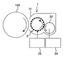
図3は、現像装置1のトナー担持ローラ2を軸線方向の一端側から示す斜視図である。同図において、トナー担持ローラ2は、ローラ部3や、これの軸線方向の両端面からそれぞれ突出する軸部材4,5などを有している。ローラ部3の周面には、ローラ軸線方向に延在する形状の複数の電極が、周方向(回転方向)に所定のピッチで並ぶように形成されている。これら電極のうち、周方向において1個おきに並んでいるもの同士は、互いに同じ電位状態にされる電気的に同相の電極になっている。具体的には、A相電極3aとB相電極3bとが周方向に交互に並ぶように配設されている。これらA相電極3a、B相電極3bは、何れもローラ部3の周面上において、軸線方向の殆どの領域に渡って延在しているが、軸線方向の両端にまでは延びていない。
FIG. 3 is a perspective view showing the
トナー担持ローラ2は、後述する現像装置内において、軸部材4,5が回転自在に支持されながら回転駆動される。図示のように、ローラ部3の軸線方向の一端面においては、軸線方向の端側から中央側に向かう円形の窪みD1が形成されている。また、同図には示していないが、ローラ部3の他端面においても、同様の窪みが形成されている。
The
図4は、ローラ部3の軸線方向における一端部を、A相電極3aの箇所で破断して示す縦断面図である。ローラ部3の表面は、絶縁性材料からなる表面保護層3dで覆われている。A相電極3aは、アクリル樹脂等からなる円柱状のローラ基体3cの表面と表面保護層3dとの間に形成されている。ローラ部3の軸線方向の一端部では、ローラ基体3cの表面上において、軸線方向の中央側から端側に向けて延びているA相電極3aが表面上をそのまま端まで伝って延びるのではなく、途中でローラ基体3cの内部を貫通して、窪みD1の内周面に至っている。そして、窪みD1の内周面上で軸線方向に沿って中央側から端側に向けて再び延びている。ローラ基体3cの表面上では表面保護層3dに覆われているが、窪みD1の内周面上では保護層に覆われておらず無垢の表面を露出させている。
FIG. 4 is a longitudinal sectional view showing one end portion of the
図5は、ローラ部3の軸線方向における一端部を、B相電極3bの箇所で破断して示す縦断面図である。軸線方向の一端部において、B相電極3bは、A相電極(3a)とは異なり、窪みD1の内周面には存在していない。ローラ基体3cの表面上だけに形成されているのである。
FIG. 5 is a longitudinal cross-sectional view showing one end portion of the
図6は、ローラ部3の軸線方向における他端部を、A相電極3aの箇所で破断して示す縦断面図である。軸線方向の他端部において、A相電極3aは、窪みD2の内周面には存在していない。ローラ基体3cの表面上だけに形成されているのである。
FIG. 6 is a longitudinal cross-sectional view showing the other end portion of the
図7は、ローラ部3の軸線方向における他端部を、B相電極3bの箇所で破断して示す縦断面図である。ローラ部3の軸線方向の他端部では、ローラ基体3cの表面上において、軸線方向の中央側から端側に向けて延びているB相電極3bが表面上をそのまま端まで伝って延びるのではなく、途中でローラ基体3cの内部を貫通して、窪みD2の内周面に至っている。そして、窪みD2の内周面上で軸線方向に沿って中央側から端側に向けて再び延びている。ローラ基体3cの表面上では表面保護層3dに覆われているが、窪みD2の内周面上では保護層に覆われておらず無垢の表面を露出させている。
FIG. 7 is a longitudinal cross-sectional view showing the other end portion of the
図8は、ローラ部3を示す平面展開模式図である。これまでの説明と、図8とからわかるように、ローラ部3の軸線方向の一端部では、A相電極3aが窪みD1の内周面まで延びているのに対し、B相電極3bは窪みD1の内周面まで延びていない。一方、ローラ部3の軸線方向の他端部では、B相電極3bが窪みD2の内周面まで延びているのに対し、A相電極3aが窪みD2の内周面まで延びていない。
FIG. 8 is a schematic plan view showing the
複数のA相電極3aやB相電極3bについては、ローラ基体3cの周面上において、例えば次のようにして形成すればよい。即ち、まず、図9に示すローラ基体3cの表面に対して切削加工を施すことで、図10に示すように、ローラ軸線方向に延在しつつローラ周方向に所定のピッチで並ぶ複数の溝3fを形成する。溝3fの幅は50[μm]程度であり、溝の周方向における配設ピッチは100[μm]程度である。次に、図11に示すように、ローラ基体3cの表面に無電解ニッケルメッキ処理を施してメッキ層3gを形成する。このメッキ層3gについては、複数の溝3fのそれぞれ内部にまで行き渡らせつつ、ローラ周面を所定の厚みで被覆するように形成する。このようにして形成したメッキ層3gのうち、溝3f内に進入していない箇所を、旋削加工によって取り除くことで、図12に示すように、互いに独立した溝3f内に固定されたA相電極3aやB相電極3bを得る。その後、ローラ基体3cの表面にシリコーン系樹脂をコーティングして、図13に示すように、厚み約5[μm]、体積抵抗率約1010[Ω・cm]の表面保護層3dを形成する。
The plurality of
窪みD1や窪みD2内には、同様の工程によってA相電極3aやB相電極3bを形成する。但し、保護層による電極の被覆は行わない。
In the recess D1 and the recess D2, the
先に図8に示したローラ部3の複数のA相電極3aには、図14に示すA相交番電圧が印加される。また、複数のB相電極3bには、図14に示すB相交番電圧が印加される。A相交番電圧と、B相交番電圧とは、図示のように互いに逆位相になっており、単位時間あたりにおける平均電位は互いに同じである。このような交番電圧が印加されると、トナー担持ローラ2におけるローラ部3の表面上のトナーが、A相電極3a上とB相電極3b上との間を往復移動するように繰り返しホッピングする。以下、トナー担持ローラ2の表面上でトナーが所定の周期でホッピングを繰り返している状態をフレア(Flare)という。
The A-phase alternating voltage shown in FIG. 14 is applied to the plurality of
A相交番電圧やB相交番電圧のピーク・ツウ・ピーク電圧(以下、Vppと記す)については、100〜1000[V]の範囲に設定することが望ましい。Vppが100[V]を下回ると、電極間に十分な強度の交番電界を形成することができずに、トナーのホッピングが良好に得られなくなるからである。また、Vppが1000[V]を超えると、電極間で放電を発生させる可能性がでてくる。放電が発生すると、電極間に交番電界を形成することができずに、トナーがホッピングしなくなる。 The peak-to-peak voltage (hereinafter referred to as Vpp) of the A-phase alternating voltage and the B-phase alternating voltage is preferably set in the range of 100 to 1000 [V]. When Vpp is less than 100 [V], an alternating electric field with sufficient strength cannot be formed between the electrodes, and toner hopping cannot be obtained satisfactorily. Further, when Vpp exceeds 1000 [V], there is a possibility of generating a discharge between the electrodes. When the discharge occurs, an alternating electric field cannot be formed between the electrodes, and the toner does not hop.
A相交番電圧やB相交番電圧の周波数fについては、0.1〜10[kHz]の範囲に設定することが望ましい。周波数fが0.1[kHz]を下回ると、ホッピングによるトナーの電極間往復移動速度が現像速度に追いつかなくなってしまうからである。また、周波数fが10[kHz]を上回ると、トナーのホッピングが電極間における交番電界の向きの切り替わり速度に追従できなくなってしまう。 The frequency f of the A-phase alternating voltage and the B-phase alternating voltage is preferably set in the range of 0.1 to 10 [kHz]. This is because if the frequency f is less than 0.1 [kHz], the reciprocating speed of the toner between the electrodes due to hopping cannot catch up with the developing speed. If the frequency f exceeds 10 [kHz], the toner hopping cannot follow the switching speed of the direction of the alternating electric field between the electrodes.
A相交番電圧やB相交番電圧の中心値については、後述する感光体の潜像電位と地肌部電位との間の値に設定する。 The center value of the A-phase alternating voltage and the B-phase alternating voltage is set to a value between the latent image potential of the photoconductor and the background portion potential described later.
なお、図示のような矩形波状の交番電圧では、極性が瞬時に切り替わるため、トナーに対して大きな静電力を付与することが可能である。但し、サイン波状の交番電圧や三角波状の交番電圧を採用してもよい。 Note that with the rectangular wave-like alternating voltage as shown in the figure, the polarity is instantaneously switched, so that a large electrostatic force can be applied to the toner. However, a sinusoidal alternating voltage or a triangular alternating voltage may be employed.
また、一方の軸部材(電極)に周波数fの矩形波状のパルス電圧を印加する一方で、もう一方の軸部材(電極)には、前記パルス電圧の平均電位となる直流電圧を印加しても、逆位相のパルス電圧を採用する場合と同様に、フレア現象を生起せしめることが可能である(図15)。この場合、電極間の最大電位差はVppの半分になるため、パルス電圧のVppを上述した交番電圧の倍の200〜2000[V]に設定することが望ましい。互いに異なる2つの交番電圧の位相を逆位相にするという制御が要らなくなるので、電源コストを低く抑えることができる。 In addition, a rectangular wave pulse voltage having a frequency f is applied to one shaft member (electrode), while a DC voltage that is an average potential of the pulse voltage is applied to the other shaft member (electrode). As in the case of using a pulse voltage having an opposite phase, it is possible to cause a flare phenomenon (FIG. 15). In this case, since the maximum potential difference between the electrodes is half of Vpp, it is desirable to set the Vpp of the pulse voltage to 200 to 2000 [V] which is twice the alternating voltage described above. Since it is not necessary to control the phase of two alternating voltages that are different from each other, the power supply cost can be kept low.
ローラ部3の周面におけるA相電極3a上とB相電極3bとの間をホッピングによる往復移動の繰り返しで、ローラ部3の周面上にフレアを形成しているトナーは、トナー担持ローラ2の回転駆動によって現像領域まで搬送される。そして、現像領域にて、その放物線状のホッピング軌跡の頂点付近で感光体(90)の静電潜像の近傍に至ると、静電潜像の静電気力によって引かれながらホッピング軌跡から外れて、静電潜像に付着する。これに対し、放物線状のホッピング軌跡の頂点付近で感光体(90)の地肌部の近傍に至ると、ホッピング軌跡から外れることなく下降して、トナー担持ローラ2の表面に着地する。
The toner forming the flare on the peripheral surface of the
ホッピングによってローラ部3との吸着力が解かれた状態のトナーを現像に用いることで、現像ローラや現像スリーブを用いる1成分現像方式や二成分現像方式では実現が望めなかったほどの低電位現像を実現することができる。
By using toner in a state in which the adsorbing force with the
先に示した図2において、現像領域で現像に寄与しなかったトナーは、トナー担持ローラ2の回転に伴ってケーシング11内に戻った後、上述のトナー供給領域に進入する。このトナー供給領域においても、トナーはホッピングによってローラ表面との付着力を発揮していないので、トナー担持ローラ2に対してカウンター方向に摺擦する磁気ブラシによって容易に掻き取られたり均されたりする。同時に、新しいトナーがトナー供給スリーブ19上の磁気ブラシから供給される。このような掻き取り回収、均し、及び供給の相乗作用により、トナー供給領域を通過した後のトナー担持ローラ12表面上には均一量のトナーがホッピングするようになる。
In FIG. 2, the toner that has not contributed to the development in the development area returns to the
次に、実施形態に係る画像形成装置の特徴的な構成について説明する。
先に示した図25において、トナー担持ローラ2の複数の電極(A相電極、B相電極)には、搬送電源25により、図14に示した電圧が印加される。この印加により、トナー担持ローラ2の表面上には、トナーをホッピングさせる電界が形成される。搬送電源25や、搬送電源25からの出力電圧を各電極に導くための後述する摺擦電極は、A相電極やB相電極に出夏を印加してトナー担持ローラ2の表面上に電界を形成する電界形成手段として機能している。
Next, a characteristic configuration of the image forming apparatus according to the embodiment will be described.
In FIG. 25 shown above, the voltage shown in FIG. 14 is applied to the plurality of electrodes (A-phase electrode, B-phase electrode) of the
図16は、トナー担持ローラ2のローラ部の周面上における領域区分を説明するための模式図である。トナー担持ローラ2のローラ部の周面上には、周方向に並ぶ4つの領域が形成されている。トナー担持ローラ2の回転方向に順に並ぶ、トナー供給領域A1、現像前搬送領域A2、現像領域A3、現像後搬送領域A4という4つの領域である。トナー担持ローラ2のローラ部の表面は、回転駆動に伴って、A1からA4の領域を順次通過していく。
FIG. 16 is a schematic diagram for explaining region division on the peripheral surface of the roller portion of the
トナー供給領域A1は、図示のように、トナー担持ローラ2のローラ部と、トナー供給ロール18とが対向している領域である。より詳しくは、トナー担持ローラ2の回転を停止させ且つローラ部3の各電極に交番電圧を印加しない状態で、トナー供給ロール18に電圧を印加したときに、トナーが付着するロール部周面領域に対向する領域である。このトナー供給領域A1において、トナー供給ロール18のトナー供給スリーブ19の表面に担持されている混合剤中のトナーが、トナー担持ローラ2のローラ部の表面上に供給される。
As shown in the figure, the toner supply area A1 is an area where the roller portion of the
現像領域A3は、これまで説明してきたように、感光体150とトナー担持ローラ2のローラ部とが対向している領域であり、ここでローラ部の表面上でホッピングしたトナーが現像に寄与する。より詳しくは、感光体150とトナー担持ローラ2とを対向させ、感光体150の駆動を停止させ、且つ表面上でフレアを形成しているトナー担持ローラ2を回転させた状態で、感光体150のベタ潜像が現像される領域である。
As described above, the development area A3 is an area where the
現像前搬送領域A2は、トナー担持ローラ2の回転方向において、トナー供給領域A1と現像領域A3との間に存在する領域である。また、現像後搬送領域A4は、トナー担持ローラ2の回転方向において、現像領域A3とトナー供給領域A4との間に存在する領域である。
The pre-development conveyance area A2 is an area that exists between the toner supply area A1 and the development area A3 in the rotation direction of the
図17は、トナー担持ローラ2を軸線方向の一端側から示す正面図である。トナー担持ローラ2のローラ部における軸線方向の一端面には、既に説明したように、窪みD1が形成されている。そして、A相電極3aは、軸線方向において、ローラ部3の表面からこの窪みD1の内周面まで延びている。窪みD1内には、A相第1摺擦電極50やA相第2摺擦電極52が、ローラ部3に連れ回らないように配設されている。これら摺擦電極には、搬送電源25によって互いに異なるA相交番電圧が印加されるようになっている。
FIG. 17 is a front view showing the
A相第1摺擦電極50は、回転するローラ部3の窪みD1の内周面のうち、現像領域A3との対向位置にある箇所に対して摺擦するように、付勢手段たるコイルバネ51によって窪みD1内周面に向けて付勢されている。これにより、窪みD1の内周面上において周方向に所定のピッチで形成されたA相電極3aのうち、ローラ部3の回転に伴って現像領域A3との対向位置に進入したものに対しては、搬送電源25から出力される現像用A相交番電圧がA相第1摺擦電極50を介して印加される。
The A-phase first rubbing
A相第2摺擦電極52は、回転するローラ部3の窪みD1の内周面のうち、現像領域A3以外の領域との対向位置にある箇所に対して摺擦するように、3つのコイルバネ53によって窪みD1内周面に向けて付勢されている。これにより、窪みD1の内周面上において周方向に所定のピッチで形成されたA相電極3aのうち、ローラ部3の回転に伴って現像領域A3以外の領域との対向位置に進入したものに対しては、搬送電源25から出力される搬送用A相交番電圧がA相第2摺擦電極52を介して印加される。
The A-phase second rubbing
現像用A相交番電圧や搬送用A相交番電圧は何れも、先に図14に示したA相交番電圧のように、B相交番電圧とは互いに逆位相の関係になっているが、両者の特性は互いに少し異なっている。具体的には、現像用A相交番電圧の方が、搬送用A相交番電圧に比べて、トナーをより高くホッピングさせる特性になっている。 Both the developing A-phase alternating voltage and the conveying A-phase alternating voltage are in opposite phases to the B-phase alternating voltage, as in the A-phase alternating voltage shown in FIG. The characteristics are slightly different from each other. Specifically, the developing A-phase alternating voltage has a characteristic of causing the toner to hop higher than the carrying A-phase alternating voltage.
図18は、トナー担持ローラ2を軸線方向の他端側から示す背面図である。トナー担持ローラ2のローラ部における軸線方向の他端面には、既に説明したように、窪みD2が形成されている。そして、B相電極3bは、軸線方向において、ローラ部3の表面からこの窪みD2の内周面まで延びている。窪みD2内には、B相第1摺擦電極54やB相第2摺擦電極56が、ローラ部3に連れ回らないように配設されている。これら摺擦電極には、搬送電源25によって互いに異なるB相交番電圧が印加されるようになっている。
FIG. 18 is a rear view showing the
B相第1摺擦電極54は、回転するローラ部3の窪みD2の内周面のうち、現像領域A3との対向位置にある箇所に対して摺擦するように、コイルバネ55によって窪みD2内周面に向けて付勢されている。これにより、窪みD2の内周面上において周方向に所定のピッチで形成されたB相電極3bのうち、ローラ部3の回転に伴って現像領域A3との対向位置に進入したものに対しては、搬送電源25から出力される現像用B相交番電圧がB相第1摺擦電極54を介して印加される。
The B-phase first rubbing
B相第2摺擦電極56は、回転するローラ部3の窪みD2の内周面のうち、現像領域A3以外の領域との対向位置にある箇所に対して摺擦するように、3つのコイルバネ57によって窪みD2内周面に向けて付勢されている。これにより、窪みD2の内周面上において周方向に所定のピッチで形成されたB相電極3bのうち、ローラ部3の回転に伴って現像領域A3以外の領域との対向位置に進入したものに対しては、搬送電源25から出力される搬送用B相交番電圧がB相第2摺擦電極56を介して印加される。
The B-phase second rubbing
現像用B相交番電圧や搬送用B相交番電圧は何れも、先に図14に示したB相交番電圧のように、A相交番電圧とは互いに逆位相の関係になっているが、両者の特性は互いに少し異なっている。具体的には、現像用B相交番電圧の方が、搬送用B相交番電圧に比べて、トナーをより高くホッピングさせる特性になっている。 Both the developing B-phase alternating voltage and the conveying B-phase alternating voltage are in opposite phases to the A-phase alternating voltage as in the B-phase alternating voltage shown in FIG. The characteristics are slightly different from each other. Specifically, the developing B-phase alternating voltage has a characteristic of causing the toner to hop higher than the conveying B-phase alternating voltage.
このように、実施形態に係る画像形成装置においては、搬送電源25や各摺擦電極等からなる電界形成手段が、次のように構成されている。即ち、トナー担持ローラ2のローラ部3における周面のうち、現像領域A3内に位置している箇所である現像領域内箇所と、現像領域外に位置している箇所である現像領域外箇所とで、周面上の電界として互いに異なる特性のものを形成する。そして、ローラ部3の現像領域内箇所におけるトナーのホッピング高さを、現像領域外箇所のトナーのホッピング高さよりも大きくする。
As described above, in the image forming apparatus according to the embodiment, the electric field forming unit including the
かかる構成の画像形成装置においては、ローラ部3の現像領域内箇所では、トナーを十分な高さまでホッピングさせ得る特性の電界をローラ部3表面上に形成して、感光体150の孤立ドットを良好に現像する。この一方で、ローラ部3の現像領域外箇所では、トナーを比較的低い高さでホッピングさせる特性の電界をローラ部表面上に形成して、トナー飛散の発生を抑える。よって、特許文献3に記載のような対向電極基板を設けることなく、孤立ドットの現像不良と、ローラ部3表面上からのトナー飛散とを抑えることができる。
In the image forming apparatus having such a configuration, an electric field having a characteristic capable of hopping the toner to a sufficient height is formed on the surface of the
なお、トナーをより高くホッピングさせ得る電界とは、具体的には、ローラ部3の表面上における表面と直交する方向の強度成分がより大きい電界であることを意味する。
Note that the electric field capable of causing the toner to hop higher means specifically that the electric field has a larger intensity component in the direction perpendicular to the surface on the surface of the
次に、実施形態に係る画像形成装置に、より特徴的な構成を付加した各実施例の画像形成装置について説明する。なお、以下に特筆しない限り、各実施例に係る画像形成装置の構成は、実施形態と同様である。 Next, the image forming apparatus of each example in which a more characteristic configuration is added to the image forming apparatus according to the embodiment will be described. Note that the configuration of the image forming apparatus according to each example is the same as that of the embodiment unless otherwise specified.
[第1実施例]
第1実施例に係る画像形成装置の搬送電源25は、図14にA相交番電圧として示した波形の交番電圧を、現像領域とは異なる領域との対向位置にあるA相電極3aに対して搬送用A相交番電圧として印加する。また、現像領域A3との対向位置に進入したA相電極3aに対して、搬送用A相交番電圧と位相や周波数が同じで且つVppが搬送用A相交番電圧よりも大きな値の交番電圧を、現像用A相交番電圧として印加する。また、図14にB相交番電圧として示した波形の交番電圧を、現像領域とは異なる領域との対向位置にあるB相電極3bに対して搬送用B相交番電圧として印加する。更には、現像領域A3との対向位置に進入したB相電極3bに対して、搬送用B相交番電圧と位相や周波数が同じで且つVppが搬送用B相交番電圧よりも大きな値の交番電圧を、現像用B相交番電圧として印加する。なお、交番電圧のVppは、現像用A相交番電圧と現像用B相交番電圧とで、互いに同じになっている。また、搬送用A相交番電圧と搬送用B相交番電圧とでも、Vppが互いに同じになっている。
[First embodiment]
The
かかる構成では、現像領域において、トナーのホッピング高さを現像領域とは異なる領域におけるトナーホッピング高さよりも大きくする電界をローラ部3の表面上に形成することができる。つまり、現像領域におけるローラ部3の表面上に形成される電界の表面と直交する方向の強度成分を、現像領域とは異なる領域のローラ部3の表面上の電界よりも大きくすることができる。
With this configuration, an electric field that makes the toner hopping height larger than the toner hopping height in an area different from the developing area in the developing area can be formed on the surface of the
本発明者らは、第1実施例に係る画像形成装置と同様の構成の試験機を試作した。この試験機においては、A相電極3aやB相電極3bとして、ローラ周方向の寸法である幅を40[μm]にしたものを採用している。また、A相電極3aとB相電極3bとの間の距離については、幅と同じ40[μm]に設定している。トナー担持ローラ2としては、ローラ部の直径を30[μm]にしたものを用いている。また、現像領域A3における感光体150とトナー担持ローラ2のローラ部とのギャップである現像ギャップについては、0.3[mm]に設定している。
The inventors have made a test machine having the same configuration as that of the image forming apparatus according to the first embodiment. In this testing machine, as the
かかる構成の試験機において、現像用A相交番電圧、現像用B相交番電圧、搬送用A相交番電圧、搬送用B相交番電圧として、それぞれ周波数を1[kHz]に設定したものを印加しながら、テスト画像をプリントした。このテストプリントにおいては、感光体150とトナー担持ローラ2とをそれぞれ180[mm/sec]の線速で回転させた。感光体150の地肌部の電位を約−400[V]とし、光書込による静電潜像の電位を−50[V]まで減衰させた。この静電潜像の解像度は600[dpi]である。トナーとしては、平均粒径を5[μm]に調整したものを用いた。
In the tester having such a configuration, a development A-phase alternating voltage, a developing B-phase alternating voltage, a transport A-phase alternating voltage, and a transport B-phase alternating voltage, each having a frequency set to 1 [kHz] are applied. A test image was printed. In this test print, the
次の表1に示す3通りの条件でテストプリントを実施し、それぞれの条件化における孤立ドットの現像性やトナー飛散抑制性を調べた。孤立ドットの現像性については、孤立1ドットを所望の画像濃度で現像できた場合を「○」、所望の現像濃度よりも薄く現像してしまったり、現像できなかったりした場合を「×」として評価した。トナー飛散抑制性については、次のようにして評価した。即ち、テストプリント時において、トナー担持ローラ2の真下に新品の白紙を敷き、トナー担持ローラ2上でトナーをホッピングさせながら、トナー担持ローラ2を1回転させて装置を停止した後、白紙のトナーによる汚れ具合を観察した。白紙にトナー汚れが認められなかった場合を「○」、認められた場合を「×」としてトナー飛散抑制性を評価した。なお、表1において、「現像用の交番電圧」とは、現像用A相交番電圧や現像用B相交番電圧を示している。また、「搬送用の交番電圧」とは、搬送用A相交番電圧や搬送用B相交番電圧を示している。

条件1では、孤立ドットの現像性が「○」という結果になっている。条件1のように、現像領域内の電極にVppが400[V](±200V)である交番電圧を印加すると、現像領域でトナーを十分な高さまでホッピングさせて孤立1ドットを十分な濃度で現像できるのである。しかし、条件1では、現像領域とは異なる領域にある電極にも、現像領域と同様にVppが400[V]である交番電圧を印加している。このような交番電圧では、表1からわかるように、トナー飛散抑制性を「×」という結果にしてしまう。現像領域とは異なる領域においては、孤立1ドットを十分な現像濃度で現像する場合と同様の高さでトナーをホッピングさせると、顕著なトナー飛散を引き起こしてしまうのである。
In
条件2では、トナー飛散抑制性が「○」という結果になっている。条件2のように、現像領域外の領域の電極にVppが200[V](±100V)である交番電圧を印加すると、顕著なトナー飛散の発生を防止することができるのである。しかし、条件1では、現像領域とは異なる領域にある電極にも、現像領外と同様にVppが200[V]である交番電圧を印加すると、現像領域でトナーを十分な高さまでホッピングさせることができずに、孤立ドットの現像不良を引き起こしてしまうのである。
In
条件3では、第1実施例に係る画像形成装置と同様に、現像用の交番電圧のVppとして、搬送用の交番電圧よりも大きくしたものを採用している。具体的には、現像用の交番電圧のVppとして400[V]を採用している。これに対し、搬送用の交番電圧のVppとしては、200[V]を採用している。かかる構成では、現像領域とトナーを十分な高さまでホッピングさせて孤立ドットを良好に現像する一方で、現像領域外におけるトナーのホッピング高さを比較的低くして、トナー飛散の発生を有効に抑えていることがわかる。
In
搬送電源25は、センサの検知結果に基づく温度や湿度の変動量が所定量を超えるなど、所定の条件が具備されたことに基づいて、現像用A相交番電圧や現像用B相交番電圧のVppを、搬送用の交番電圧とは独立して変化させるようになっている。かかる構成では、温湿度変動などにより、トナーのホッピング特性が変化した場合に、その変化量に基づいて現像用A相交番電圧や現像用B相交番電圧のVppを変化させることで、現像領域において安定したホッピング高さを得ることができる。
The
また、搬送電源25は、センサの検知結果に基づく温度や湿度の変動量が所定量を超えるなど、所定の条件が具備されたことに基づいて、搬送用A相交番電圧や搬送用B相交番電圧のVppを、現像用の交番電圧とは独立して変化させるようになっている。かかる構成では、温湿度変動などにより、トナーのホッピング特性が変化した場合に、その変化量に基づいて搬送用A相交番電圧や搬送用B相交番電圧のVppを変化させることで、現像領域とは異なる領域において安定したホッピング高さを得ることができる。
Further, the
[第2実施例]
第2実施例に係る画像形成装置の搬送電源25は、図14にA相交番電圧として示した波形の交番電圧を、現像領域とは異なる領域との対向位置にあるA相電極3aに対して搬送用A相交番電圧として印加する。また、現像領域A3との対向位置に進入したA相電極3aに対して、搬送用A相交番電圧とVppが同じで且つ搬送用A相交番電圧よりも周波数fが小さい交番電圧を、現像用A相交番電圧として印加する。また、図14にB相交番電圧として示した波形の交番電圧を、現像領域とは異なる領域との対向位置にあるB相電極3bに対して搬送用B相交番電圧として印加する。更には、現像領域A3との対向位置に進入したB相電極3bに対して、搬送用B相交番電圧とVppが同じで且つ搬送用B相交番電圧よりも周波数fが小さい交番電圧を、現像用B相交番電圧として印加する。なお、周波数は、現像用A相交番電圧と現像用B相交番電圧とで、互いに同じになっており、互いの波形の位相も同期している。また、搬送用A相交番電圧と搬送用B相交番電圧とでも、周波数が互いに同じになっており、互いの波形の位相も同期している。
[Second Embodiment]
The
かかる構成では、現像領域において、トナーのホッピング高さを現像領域とは異なる領域におけるトナーホッピング高さよりも大きくする電界をローラ部3の表面上に形成することができる。つまり、現像領域におけるローラ部3の表面上に形成される電界の表面と直交する方向の強度成分を、現像領域とは異なる領域のローラ部3の表面上の電界よりも大きくすることができる。これは次に説明する理由からである。即ち、交番電圧の周波数fを大きくするほど、トナーのホッピングによる電極間での往復移動周期が長くなって、トナーのホッピング高さが大きくなる。これに対し、交番電圧の周波数fを小さくするほで、トナーのホッピングによる電極間での往復移動周期が短くなって、トナーのホッピング高さが小さくなる。
With this configuration, an electric field that makes the toner hopping height larger than the toner hopping height in an area different from the developing area in the developing area can be formed on the surface of the
本発明者らは、上述した試験機を用いて、次の表2に示す3通りの条件でテストプリントを実施し、それぞれの条件化における孤立ドットの現像性やトナー飛散抑制性を先の実験と同様にして調べた。なお、Vppについては、現像用A相交番電圧、搬送用A相交番電圧、現像用B相交番電圧、搬送用B相交番電圧の何れにおいても、300[V]に設定した。
条件Aでは、孤立ドットの現像性が「○」という結果になっている。条件Aのように、Vppが300[V]であって且つ現像領域内の電極に周波数が0.5[kHz]である交番電圧を印加すると、現像領域でトナーを十分な高さまでホッピングさせて孤立1ドットを十分な濃度で現像できるのである。しかし、条件Aでは、現像領域とは異なる領域にある電極にも、現像領域と同じ交番電圧を印加している。このような交番電圧では、表2からわかるように、トナー飛散抑制性を「×」という結果にしてしまう。現像領域とは異なる領域においては、孤立1ドットを十分な現像濃度で現像する場合と同様の高さでトナーをホッピングさせると、顕著なトナー飛散を引き起こしてしまうのは、先に述べた通りである。 Under the condition A, the developability of the isolated dots is “◯”. As in Condition A, when an alternating voltage having a Vpp of 300 [V] and a frequency of 0.5 [kHz] is applied to the electrodes in the development area, the toner is hopped to a sufficient height in the development area. One isolated dot can be developed with a sufficient density. However, under the condition A, the same alternating voltage as that in the development region is applied to the electrode in a region different from the development region. With such an alternating voltage, as can be seen from Table 2, the result of the toner scattering suppression is “x”. As described above, in an area different from the development area, if toner is hopped at the same height as when developing an isolated dot with a sufficient development density, the toner scatters significantly. is there.
条件Bでは、トナー飛散抑制性が「○」という結果になっている。条件Bのように、現像領域外の領域の電極にVppが300[V]で且つ周波数が5[kHz]である交番電圧を印加すると、顕著なトナー飛散の発生を防止することができるのである。しかし、条件Bでは、現像領域とは異なる領域にある電極にも、現像領外と同様の交番電圧を印加している。そして、現像領域でトナーを十分な高さまでホッピングさせることができずに、孤立ドットの現像不良を引き起こしている。 Under condition B, the toner scattering suppression property is “◯”. As in Condition B, when an alternating voltage having a Vpp of 300 [V] and a frequency of 5 [kHz] is applied to the electrode outside the development area, the occurrence of significant toner scattering can be prevented. . However, under the condition B, an alternating voltage similar to that outside the development region is applied to an electrode in a region different from the development region. In addition, the toner cannot be hopped to a sufficient height in the development area, causing a defective development of isolated dots.
条件Cでは、第2実施例に係る画像形成装置と同様に、現像用の交番電圧の周波数として、搬送用の交番電圧よりも小さくしたものを採用している。具体的には、現像用の交番電圧の周波数として0.5[kHz]を採用している。これに対し、搬送用の交番電圧のVppとしては、5[kHz]を採用している。かかる構成では、現像領域とトナーを十分な高さまでホッピングさせて孤立ドットを良好に現像する一方で、現像領域外におけるトナーのホッピング高さを比較的低くして、トナー飛散の発生を有効に抑えていることがわかる。 In the condition C, as in the image forming apparatus according to the second embodiment, the frequency of the alternating voltage for development is smaller than the alternating voltage for conveyance. Specifically, 0.5 [kHz] is adopted as the frequency of the alternating voltage for development. On the other hand, 5 [kHz] is adopted as the alternating voltage Vpp for conveyance. In such a configuration, the development area and the toner are hopped to a sufficient height to develop the isolated dots well, while the toner hopping height outside the development area is relatively low to effectively suppress the occurrence of toner scattering. You can see that
搬送電源25は、センサの検知結果に基づく温度や湿度の変動量が所定量を超えるなど、所定の条件が具備されたことに基づいて、現像用A相交番電圧や現像用B相交番電圧の周波数を、搬送用の交番電圧とは独立して変化させるようになっている。かかる構成では、温湿度変動などにより、トナーのホッピング特性が変化した場合に、その変化量に基づいて現像用A相交番電圧や現像用B相交番電圧の周波数を変化させることで、現像領域において安定したホッピング高さを得ることができる。
The
また、搬送電源25は、センサの検知結果に基づく温度や湿度の変動量が所定量を超えるなど、所定の条件が具備されたことに基づいて、搬送用A相交番電圧や搬送用B相交番電圧の周波数を、現像用の交番電圧とは独立して変化させるようになっている。かかる構成では、温湿度変動などにより、トナーのホッピング特性が変化した場合に、その変化量に基づいて搬送用A相交番電圧や搬送用B相交番電圧の周波数を変化させることで、現像領域とは異なる領域において安定したホッピング高さを得ることができる。
Further, the
次に、本発明を適用した各変形例の画像形成装置について説明する。なお、以下に特筆しない限り、各変形例に係る画像形成装置の構成は、第1実施例又は第2実施例と同様である。 Next, image forming apparatuses according to modified examples to which the present invention is applied will be described. Unless otherwise specified, the configuration of the image forming apparatus according to each modification is the same as that of the first embodiment or the second embodiment.
[第1変形例]
図19は、第1変形例に係る画像形成装置の感光体150と現像装置1とを示す要部構成図である。現像装置1内のトナー収容部には、非磁性トナーが収容されており、この非磁性トナーは回転駆動される2本の撹拌ローラ59によって撹拌される。そして、互いに当接しながら回転する2本の撹拌ローラ59の当接部で摺擦さしめられることで摩擦帯電する。摩擦帯電した非磁性トナーは、回転するトナー供給ローラ30の表面に汲み上げられる。そして、自らの自由端側をトナー供給ローラ30に当接させている規制部材22に押し付けられて、層厚が規制される。この後、トナー供給ローラ30の回転に伴って、トナー担持ローラ2に対向するトナー供給領域まで搬送される。
[First Modification]
FIG. 19 is a main part configuration diagram showing the
トナー供給ローラ30には、供給バイアス電源24によって供給バイアスが印加されている。この供給バイアスは、直流電圧でも交流電圧でもよい。また直流電圧に交流電圧を重畳させた電圧でもよい。トナー供給領域においては、トナー担持ローラ2の各電極に印加される交番電圧の平均値と、供給バイアスとの電位差により、非磁性トナーをトナー供給ローラ30側からトナー担持ローラ側に向けて移動させる供給電界が形成されている。この供給電界により、トナー供給ローラ30の表面上の非磁性トナーがトナー担持ローラ2のローラ部の表面に移動する。
A supply bias is applied to the
トナー供給領域でトナー担持ローラ2のローラ部の表面に供給された非磁性トナーは、ローラ部の表面上でホッピングしてフレアを形成しながら、トナー担持ローラ2の回転に伴って現像領域に向けて搬送される。そして、フレアを形成している非磁性トナーの一部は、現像領域で現像に寄与する。現像に寄与しなかった非磁性トナーは、トナー担持ローラ2のローラ部の表面で引き続きフレアを形成しながら、トナー担持ローラ2の回転に伴ってケーシング11内に戻る。そして、図示しない回収手段によってローラ部の表面上から回収される。回収された非磁性トナーは、トナー収容部内に戻された後、再びトナー担持ローラ2のローラ部に供給される。
The non-magnetic toner supplied to the surface of the roller portion of the
[第2変形例]
図20は、第2実施例に係る画像形成装置を示す概略構成図である。この画像形成装置は、マゼンタ,シアン,イエロー,ブラック(以下、M,C,Y,Kという)のトナー像を重ね合わせてフルカラー画像を形成することができる。そして、ベルトユニット81、4色にそれぞれ個別に対応する4つのプロセスユニット、4つの光書込ユニット100M,C,Y,K、レジストローラ対79、転写ローラ87、定着装置76、給紙カセット78などを備えている。
[Second Modification]
FIG. 20 is a schematic configuration diagram illustrating an image forming apparatus according to the second embodiment. This image forming apparatus can form a full-color image by superimposing magenta, cyan, yellow, and black (hereinafter referred to as M, C, Y, and K) toner images. The
ベルトユニット81は、潜像担持体たる無端ベルト状の感光体150を、水平方向よりも鉛直方向にスペースをとる縦長の姿勢で張架しながら図中反時計回り方向に無端移動せしめる。より詳しくは、無端ベルト上の感光体150を、駆動ローラ83、テンションローラ84、転写バックアップローラ85、及び4つの現像対向ローラ86M,C,Y,Kによって裏面側から支えながら張架している。そして、図示しない駆動手段によって図中反時計回り方向に回転駆動せしめられる駆動ローラ83の回転によって感光体150を無端移動せしめる。この感光体150における図中左側の張架面(以下、左側張架面という)は、ほぼ鉛直方向に延在する姿勢になっている。
The
感光体150の左側張架面の図中左側方には、M,C,Y,K用のプロセスユニットが鉛直方向に並ぶように配設されており、それぞれ感光体150の左側張架面に対向している。これら4つのプロセスユニットは、それぞれ、現像装置(1M,C,Y,K)と、感光体150を一様帯電せしめる帯電装置(62M,C,Y,K)とを1つのユニットとして図示しない共通の保持体に保持している。そして、図21に示すように、プリンタ筺体に対して現像装置及び帯電装置が一体的に着脱されるようになっている。
Process units for M, C, Y, and K are arranged in the vertical direction on the left side of the left-side stretched surface of the
先に示した図20において、4つの現像装置1M,C,Y,Kのうち、鉛直方向の最も下側に位置するK用の現像装置1Kの上方には、K用の帯電装置62Kが感光体150の左側張架面に対向するように配設されている。また、K用の現像装置1Kの真上に配設されたY用の現像装置1Yの上方には、Y用の帯電装置62Yが感光体150の左側張架面に対向するように配設されている。また、Y用の現像装置1Yの真上に配設されたC用の現像装置1Cの上方には、C用の帯電装置62Cが感光体150の左側張架面に対向するように配設されている。更に、Y用の現像装置1Yの真上に配設されたM用の現像装置1Mの上方には、M用の帯電装置62Mが感光体150の左側張架面に対向するように配設されている。
In FIG. 20 shown above, among the four developing
鉛直方向に並ぶ4つの現像装置1M,C,Y,Kの図中左側方には、4つの光書込ユニット100M,C,Y,Kが鉛直方向に並ぶように配設されている。これら光書込ユニット100M,C,Y,Kは、外部の図示しないパーソナルコンピュータやスキャナから送られてくる画像情報に基づいて、図示しない4つの半導体レーザーを駆動してM,C,Y,K用の書込光Lm,Lc,Ly,Lkを出射する。そして、これらを図示しないポリゴンミラーによって偏向せしめながら、図示しない反射ミラーで反射させたり光学レンズに通したりすることで感光体150に対する光走査を行う。かかる構成のものに代えて、LEDアレイによって光走査を行うものを用いてもよい。なお、光走査は暗中にて行われる。
Four
感光体150は、自らを張架している複数の張架ローラのうち、最も下方に位置する駆動ローラ83と、最も上方に位置するテンションローラ84との間では、鉛直方向上方から下方に向けてほぼ真っ直ぐに移動する。この過程において、まず、M用の帯電装置62Mとの対向位置を通過する際に、例えば負極性に一様帯電せしめられる。そして、M用の書込光Lmによる光走査によってM用の静電潜像を担持した後、M用の現像装置1Mとの対向位置を通過する。この際、感光体150に書き込まれたM用の静電潜像がM用の現像装置1Mによって現像されてMトナー像になる。
Among the plurality of stretching rollers that stretch the
Mトナー像が形成された感光体150は、鉛直方向上方から下方に向けての移動に伴って、C用の帯電装置62Cによって再び一様帯電せしめられた後、C用の書込光Lcによる光走査によってC用の静電潜像を担持する。このC用の静電潜像は、C用の現像装置1Cによって現像されてCトナー像となる。このとき、Cトナー像の全領域又は一部領域は、既に感光体150上に形成されているMトナー像に重ね合わせて現像される。そして、その重ね合わせ箇所は、M及びCによる2次色部となる。
The
Cトナー像が形成された感光体150は、鉛直方向上方から下方に向けての移動に伴って、Y用の帯電装置62Yによって再び一様帯電せしめられた後、Y用の書込光Lyによる光走査によってY用の静電潜像を担持する。このY用の静電潜像は、Y用の現像装置1Yによって現像されてYトナー像となる。このとき、Yトナー像の全領域又は一部領域は、既に感光体150上に形成されているMトナー像、Cトナー像、あるいはMC2次色部の上に重ね合わせた状態で現像される。そして、その重ね合わせ箇所は、MY2次色部、CY2次色部、あるいはMCY3次色部となる。
The
Yトナー像が形成された感光体150は、鉛直方向上方から下方に向けての移動に伴って、K用の帯電装置62Kによって再び一様帯電せしめられた後、K用の書込光Lkによる光走査によってK用の静電潜像を担持する。このK用の静電潜像は、K用の現像装置1Kによって現像されてKトナー像となる。
The
以上のようなM,C,Y,Kトナー像の重ね合わせ現像により、感光体150のおもて面(ループ外面)には、4色重ね合わせトナー像が形成される。なお、M,C,Y,K用の帯電装置62M,C,Y,Kとしては、それぞれコロナ放電によって感光体150を一様帯電せしめるものが用いられている。
By superimposing and developing the M, C, Y, and K toner images as described above, a four-color superimposed toner image is formed on the front surface (loop outer surface) of the
K用の現像装置1Kとの対向位置であるK用の現像領域を通過した感光体150は、駆動ローラ83に対する掛け回し箇所を通過すると、今度は相対的に鉛直方向下方から上方に向けて移動するようになる。そして、転写バックアップローラ85に対する掛け回し箇所に進入する。この掛け回し箇所の一部に対しては、転写ローラ87がおもて面側から当接して転写ニップを形成している。転写バックアップローラ85は接地されているのに対し、導電性の転写ローラ87には図示しないバイアス印加手段によって転写バイアスが印加されている。これにより、転写ニップを間に挟んでいる転写バックアップローラ85と転写ローラ87との間には、感光体150上のトナー像を転写バックアップローラ85側から転写ローラ87側に静電移動させる転写電界が形成されている。
The
一方、給紙カセット78は、所定のタイミングで給紙ローラ78aを回転駆動させることで、カセット内に収容している記録紙Pを給紙路に向けて送り出す。送り出された記録紙Pは、転写ニップの図中下方に配設されたレジストローラ対79のローラ間に挟み込まれる。レジストローラ対79は、記録紙Pの先端部を挟み込むとすぐに回転駆動を一時停止する。そして、記録紙Pを感光体150の4色重ね合わせトナー像と同期させ得るタイミングで回転駆動を再開して、記録紙Pを転写ニップに送り出す。
On the other hand, the
転写ニップで記録紙Pに密着せしめられた4色重ね合わせトナー像は、ニップ圧や転写電界の作用によってベルトから記録紙Pに一括転写され、記録紙Pの白色と相まってフルカラー画像となる。このようにしてフルカラー画像が形成された記録紙Pは、転写ニップから定着装置76に送り込まれた後、機外へと排出される。
The four-color superimposed toner image brought into intimate contact with the recording paper P at the transfer nip is collectively transferred from the belt to the recording paper P by the action of the nip pressure and the transfer electric field, and becomes a full color image combined with the white color of the recording paper P. The recording paper P on which a full-color image has been formed in this manner is sent from the transfer nip to the fixing
図22は、K用のプロセスユニットを感光体150とともに示す拡大構成図である。同図の現像装置1Kにおいて、トナー担持ローラ2Kの現像後搬送領域に対向する現像後対向電極28Kは、振動子32Kに片持ち支持されており、その自由端側をトナー担持ローラ2Kに対向させている。
FIG. 22 is an enlarged configuration diagram showing the K process unit together with the
現像領域(A3)で現像に寄与しなかったKトナーは、トナー担持ローラ2Kの現像後搬送領域(A4)まで進んだ後、現像後バイアスが印加される現像後対向電極28Kの表面に転移する。この転移により、トナー担持ローラ2Kの現像後搬送領域(A4)からKトナーが回収される。
K toner that has not contributed to development in the development area (A3) proceeds to the post-development transport area (A4) of the
プリントジョブ後などといった、現像動作が行われないタイミングが到来すると、上述の現像後バイアスの印加が停止される。この後、現像後対向電極28Kに接続されている図示しないリレースイッチの作動により、現像後対向電極28Kが接地された状態で、加振手段たる振動子32Kが作動して現像後対向電極28Kの表面上からKトナーが振り落とされる。そして、自重によってトナー供給スリーブ19K上の磁気ブラシとの接触位置まで落下して、磁気ブラシ内に取り込まれる。
When the timing at which the development operation is not performed, such as after a print job, is reached, the application of the post-development bias is stopped. Thereafter, the operation of a relay switch (not shown) connected to the
なお、現像後対向電極28Kについては、その表面上からのKトナーの滑り落ちを促す目的で、図示のようにトナー付着面に傾斜を設けた姿勢で配設することが望ましい。
Note that the
また、プリントジョブ後などのタイミングで、現像後対向電極28Kに印加するバイアスをKトナーと同極性のバイアスに切り替えて、現像後対向電極28KKからトナー担持ローラ2KにKトナーを再転移させるものを用いてもよい。
Further, at a timing after a print job, the bias applied to the
K用の現像装置1Kについて詳しく説明してきたが、他色用の現像装置(1M,C,Y)は、K用のものと同様の構成になっているので、説明を省略する。また、帯電装置の他に、あるいは帯電装置に加えて、クリーニング手段、感光体などを一体的にしてプロセスユニットを構成してもよい。
Although the developing
[第3変形例]
第3変形例に係る画像形成装置は、以下に説明する点の他が、第2変形例に係る画像形成装置と同様の構成になっている。
図23は、第3変形例に係る画像形成装置におけるK用のプロセスユニットを感光体150とともに示す拡大構成図である。同図において、現像装置1Kは、現像後対向電極としての現像後対向ローラ33Kを有している。この現像後対向ローラ33Kは、現像後バイアス電源29KによってKトナーとは逆極性の現像後バイアスが印加されながら、図示しない駆動手段によって図中反時計回り方向に回転駆動される。
[Third Modification]
The image forming apparatus according to the third modified example has the same configuration as the image forming apparatus according to the second modified example, except for the points described below.
FIG. 23 is an enlarged configuration diagram showing the K process unit together with the
現像領域で現像に寄与しなかったKトナーは、現像後搬送領域(A4)において、トナー担持ローラ2Kの表面上から現像後対向ローラ33Kの表面上に転移する。そして、現像後対向ローラ33Kの回転に伴って、現像後対向ローラ33Kと、分離手段たるクリーニングブレード34Kとの当接部に至ると、クリーニングブレード34Kによって現像後対向ローラ33Kの表面から掻き落とされる。その後は、自重によってトナー供給スリーブ2Kの表面上における磁気ブラシとの接触位置まで落下して、磁気ブラシ内に取り込まれる。
The K toner that has not contributed to development in the development area is transferred from the surface of the
現像後対向ローラ33Kについては、図示のように、トナー担持ローラ2Kとの対向位置においてその表面をトナー担持ローラ2Kの表面と同方向に移動させる向きで回転させることことが望ましい。更に、現像後対向ローラ33Kの線速(表面移動速度)については、トナー担持ローラ2Kの線速よりも速くすることが望ましい。このようにすることで、現像後対向ローラ33Kとの対向位置に進入してきたトナー担持ローラ2K上のKトナーに対し、現像後対向ローラ33Kにおけるトナー付着のない無垢の表面を対向させて、その無垢の表面にトナーを良好に転移させることができるからである。
As shown in the figure, the
[第4変形例]
図24は、第4変形例に係る画像形成装置におけるK用のプロセスユニットを感光体150とともに示す拡大構成図である。この画像形成装置も、各色の現像装置(1M,C,Y,K)の構成が第2変形例に係る画像形成装置と異なっているが、その他の点は第2変形例に係る画像形成装置と同様になっている。
[Fourth Modification]
FIG. 24 is an enlarged configuration diagram illustrating the K process unit together with the
同図において、現像装置1Kは、現像後対向電極の代わりに、回収ブラシローラ35Kを有している。そして、この回収ブラシローラ35Kは、軸受けによって回転自在に支持される金属製の回転軸部材と、これの周面に立設せしめられた複数の導電性の起毛からなるブラシ部とを具備している。
In the figure, the developing
現像後バイアス電源29KによってKトナーとは逆極性のバイアスが回転軸部材に印加されている回収ブラシローラ35Kは、複数の起毛からなるブラシ部の先端をトナー担持ローラ2Kの現像後搬送領域(A4)に接触させながら、その接触部でブラシ部をトナー担持ローラ2Kの表面移動方向とは逆方向に移動させる向きで回転駆動される。これにより、ブラシ部とトナー担持ローラ2Kとが接触している位置では、トナー担持ローラ2K上のKトナーがブラシ部によって掻き取られながら、バイアスの作用によってブラシ内に転移、捕捉される。
The
ブラシ部内に捕捉されたKトナーは、ブラシ回転軸線方向に延在しながらブラシ部に接触するように配設された分離手段たるフリッカー棒36Kによって起毛が弾かれる際の衝撃により、ブラシ部内から振り落とされる。フリッカー棒36Kの代わりにバイアスローラをブラシ先端に接触させてもよい。フリッカー棒36Kによってブラシ部から振り落とされたKトナーは、自重によってトナー供給スリーブ2Kの表面上における磁気ブラシとの接触位置まで落下して、磁気ブラシ内に取り込まれる。
The K toner trapped in the brush part is shaken from the brush part due to the impact when the fluffed
[第5変形例]
図25は、第5変形例に係る画像形成装置におけるK用のプロセスユニットを感光体150とともに示す拡大構成図である。この画像形成装置も、各色の現像装置(1M,C,Y,K)の構成が第2変形例に係る画像形成装置と異なっているが、その他の点は第2変形例に係る画像形成装置と同様になっている。
[Fifth Modification]
FIG. 25 is an enlarged configuration diagram illustrating the K process unit together with the
同図において、現像装置1Kは、現像後対向電極の代わりに、吸引部材たる吸引ノズル37Kを有している。
In the figure, the developing
吸引ノズル37Kには、中継管を介して吸引ポンプ39Kの吸引部が接続されている。この吸引ポンプ39Kの吐出部には排気管が接続されており、更にこの排気管の末端部は、現像装置1Kの第1収容部13Kに接続されている。
A suction part of a
吸引ポンプ39Kが作動すると、吸引ノズル37Kの吸引口の付近にある空気が、吸引口内に吸い込まれる。このとき、トナー担持ローラ2Kの現像後搬送領域上において、吸引口の付近でホッピングしているKトナーが空気とともに吸引口内に吸い込まれて、トナー担持ローラ2K上から回収される。そして、中継管、吸引ポンプ39K、吐出管内を順次経た後、現像装置1Kの第1収容部13Kに戻される。
When the
吸引ノズル37Kの吸引口回りにおけるトナー搬送方向下流側には、シール部材38Kを片持ち支持させており、これの自由端側をトナー担持ローラ2Kに接触させている。これにより、トナー供給スリーブ19KKの周りの空気を磁気ブラシ内のKトナーとともに吸引してしまうといった事態が回避されている。更に、ホッピングしながらトナー供給スリーブ2Kとともに回転するKトナーをシール部材38Kとの突き当たりによって堰き止めて、吸引口との対向位置に拘束している。
A
吸引ノズル37Kの先端と。トナー担持ローラ2Kの表面との間隙については、数十〜数百[μm]であって、且つトナー担持ローラ2Kの表面上におけるKトナーのホッピング高さよりも小さい値、にすることが望ましい。
The tip of the
吸引ポンプ39Kとしては、ダイアフラムポンプ、モーノポンプなど、Kトナーのような粉体を吸引することができるものを採用している。
As the
なお、中間転写ベルト、転写ドラム、中間転写ドラムなどを用いたカラ−画像形成装置、モノクロ画像形成装置などにも本発明の適用が可能である。 Note that the present invention can also be applied to a color image forming apparatus, a monochrome image forming apparatus, and the like using an intermediate transfer belt, a transfer drum, an intermediate transfer drum, and the like.
図26は、第6変形例に係る画像形成装置の感光体150と現像装置1とを示す要部構成図である。この画像形成装置は、第1実施例や第2実施例に係る画像形成装置と同様に、単色の画像を形成するものであり、感光体150と現像装置1とを1つずつ有している。
FIG. 26 is a main part configuration diagram showing the
現像装置1は、トナー収容部にトナーを収容している。トナー収容部には、トナーの他、トナー供給ローラ30が収容されている。トナー供給ローラ30におけるスポンジ等の弾性材料からなるローラ部をトナー担持ローラ2に接触させながら、接触部でローラ部表面をトナー担持ローラ2とは逆方向に移動させるように、トナー供給ローラ30を回転させている。トナー供給ローラ30上のトナーは、トナー担持ローラ2とトナー供給ローラ30との接触部で摺擦せしめられて摩擦帯電が促されながら、トナー担持ローラ2上に転移する。
The developing
同図では、トナー供給ローラ30の表面をトナー担持ローラ2との接触部でトナー担持ローラ2の表面とは逆方向に移動させる構成を示しているが、順方向に移動させてもよい。トナー供給ローラ30には供給バイアス電源24によって供給バイアスが印加されている。この供給バイアスの調整により、トナー供給ローラ30からトナー担持ローラ2へのトナー供給量を制御することが可能である。この供給バイアスは、直流電圧でも交流電圧でもよい。また直流電圧に交流電圧を重畳させた電圧でもよい。
In the drawing, the surface of the
これまで、互いに隣り合う2つの電極の間でトナーを往復移動させるようにホッピングせしめてフレア現象を得ながら、トナー担持体の表面移動によってトナーを現像領域まで搬送する画像形成装置の実施形態について説明してきたが、次のような画像形成装置にも、本発明の適用が可能である。即ち、特許文献1に記載の方式のように、トナー担持体において、ある電極の上からこれに隣り合う電極の上に向けてのホッピングを、トナー担持体の一端側から他端側に向かう方向で繰り返して行わせることで、トナーを現像領域に向けて搬送する画像形成装置である。また、このようなホッピングによるトナーの移動と、トナー担持体の表面移動との両方によってトナーを現像領域に向けて搬送する画像形成装置にも、本発明の適用が可能である。
So far, an embodiment of an image forming apparatus that conveys toner to a developing region by moving the surface of a toner carrier while hopping so as to reciprocate the toner between two adjacent electrodes and obtaining a flare phenomenon will be described. However, the present invention can also be applied to the following image forming apparatus. That is, as in the method described in
以上、第1実施例に係る画像形成装置においては、トナー担持ローラ2のローラ部3における複数の電極のうち、ローラ部3の現像領域内箇所に担持されているトナーのホッピングに寄与する電極と、現像領域外箇所に担持されているトナーのホッピングに寄与する電極とで、印加電圧の値であるVppを異ならせることで、ローラ部3における現像領域内箇所と現像領域外箇所とで、電界として互いに異なる特性のものを形成するように、搬送電源25等からなる電界形成手段を構成している。かかる構成では、現像領域でトナーをホッピングさせるための交番電圧のVppと、現像領域外でトナーをホッピングさせるための交番電圧のVppとを異ならせるという簡単な構成により、現像領域内箇所の上に形成される電界と、現像領域外箇所に形成される電界とで、互いに特性を異ならせることができる。
As described above, in the image forming apparatus according to the first embodiment, among the plurality of electrodes in the
また、第1実施例に係る画像形成装置においては、温湿度変化量が所定量を上回るなどといった所定の条件が具備されたことに基づいて、ローラ部3の現像領域内箇所に担持されているトナーのホッピングに寄与する電極に対する現像用の交番電圧のVppを変化させるように、電界形成手段を構成している。かかる構成では、トナーのホッピング特性の変化にかかわらず、現像領域において安定したホッピング高さを得ることができる。
Further, in the image forming apparatus according to the first embodiment, the
また、第1実施例に係る画像形成装置においては、所定の条件が具備されたことに基づいて、ローラ部3の現像領域外箇所に担持されているトナーのホッピングに寄与する電極に対する搬送用の交番電圧のVppを変化させるように、電界形成手段を構成している。かかる構成では、トナーのホッピング特性の変化にかかわらず、現像領域とは異なる領域において安定したホッピング高さを得ることができる。
Further, in the image forming apparatus according to the first embodiment, based on the fact that the predetermined condition is satisfied, the image forming apparatus is used for transporting the electrode that contributes to the hopping of the toner carried outside the developing area of the
また、第1実施例に係る画像形成装置においては、ローラ部3の現像領域内箇所に担持されているトナーのホッピングに寄与する電極に対する現像用の交番電圧のVppを、ローラ部3の現像領域外箇所に担持されているトナーのホッピングに寄与する電極に対する搬送用の交番電圧のVppよりも大きくするように、電界形成手段を構成している。かかる構成では、現像領域において、トナーのホッピング高さを現像領域とは異なる領域におけるトナーホッピング高さよりも大きくする電界をローラ部3の表面上に形成することができる。
In the image forming apparatus according to the first embodiment, the alternating voltage Vpp for development with respect to the electrode contributing to the hopping of the toner carried in the development region of the
また、第2実施例に係る画像形成装置においては、ローラ部3における複数の電極のうち、ローラ部3の現像領域内箇所に担持されているトナーのホッピングに寄与する電極と、ローラ部3の現像領域外箇所に担持されているトナーのホッピングに寄与する電極とで、交番電圧の周波数を異ならせることで、現像領域内箇所と現像領域外箇所とで、電界として互いに異なる特性のものを形成するように、電界形成手段を構成している。かかる構成では、現像領域でトナーをホッピングさせるための交番電圧の周波数と、現像領域外でトナーをホッピングさせるための交番電圧の周波数とを異ならせるという簡単な構成により、現像領域内箇所の上に形成される電界と、現像領域外箇所に形成される電界とで、互いに特性を異ならせることができる。
In the image forming apparatus according to the second embodiment, among the plurality of electrodes in the
また、第2実施例に係る画像形成装置においては、所定の条件が具備されたことに基づいて、ローラ部3の現像領域内箇所に担持されているトナーのホッピングに寄与する電極に対する現像用の交番電圧の周波数を変化させるように、電界形成手段を構成している。かかる構成では、トナーのホッピング特性の変化にかかわらず、現像領域において安定したホッピング高さを得ることができる。
Further, in the image forming apparatus according to the second embodiment, based on the fact that the predetermined condition is satisfied, the development for the electrode that contributes to the hopping of the toner carried in the development region of the
また、第2実施例に係る画像形成装置においては、所定の条件が具備されたことに基づいて、ローラ部3の現像領域外箇所に担持されているトナーのホッピングに寄与する電極に対する搬送用の交番電圧の周波数を変化させるように、電界形成手段を構成している。かかる構成では、トナーのホッピング特性の変化にかかわらず、現像領域とは異なる領域において安定したホッピング高さを得ることができる。
Further, in the image forming apparatus according to the second embodiment, based on the fact that the predetermined condition is satisfied, the image forming apparatus for transporting the electrode that contributes to the hopping of the toner carried outside the developing area of the
また、第2実施例に係る画像形成装置においては、ローラ部3の現像領域内箇所に担持されているトナーのホッピングに寄与する電極に対する現像用の交番電圧の周波数を、ローラ部3の現像領域外箇所に担持されているトナーのホッピングに寄与する電極に対する搬送用の交番電圧の周波数よりも小さくするように、電界形成手段を構成している。かかる構成では、現像領域において、トナーのホッピング高さを現像領域とは異なる領域におけるトナーホッピング高さよりも大きくする電界をローラ部3の表面上に形成することができる。
In the image forming apparatus according to the second embodiment, the frequency of the alternating voltage for development with respect to the electrode that contributes to the hopping of the toner carried in the development region of the
1:現像装置
2:トナー担持ローラ(トナー担持体)
3a:A相電極
3b:B相電極
25:搬送電源(電界形成手段の一部)
45:クリーニング装置(クリーニング手段)
50:A相第1摺擦電極(電界形成手段の一部)
51:コイルバネ(電界形成手段の一部)
52:A相第2摺擦電極(電界形成手段の一部)
53:コイルバネ(電界形成手段の一部)
54:B相第1摺擦電極(電界形成手段の一部)
55:コイルバネ(電界形成手段の一部)
56:B相第2摺擦電極(電界形成手段の一部)
57:コイルバネ(電界形成手段の一部)
62:帯電装置(帯電手段)
87:転写ローラ(転写手段)
150:感光体(潜像担持体)
A1:トナー供給領域(現像領域外)
A2:現像前搬送領域(現像領域外)
A3:現像領域
A4:現像後搬送領域(現像領域外)
1: Developing device 2: Toner carrying roller (toner carrying member)
3a: A
45: Cleaning device (cleaning means)
50: Phase A first rubbing electrode (part of electric field forming means)
51: Coil spring (part of electric field forming means)
52: Phase A second rubbing electrode (part of electric field forming means)
53: Coil spring (part of electric field forming means)
54: Phase B first rubbing electrode (part of electric field forming means)
55: Coil spring (part of electric field forming means)
56: Phase B second rubbing electrode (part of electric field forming means)
57: Coil spring (part of electric field forming means)
62: Charging device (charging means)
87: Transfer roller (transfer means)
150: Photoconductor (latent image carrier)
A1: Toner supply area (outside development area)
A2: Transport area before development (outside development area)
A3: Development area A4: Post development development area (outside development area)
Claims (10)
上記電界形成手段が、上記複数の電極のうち、上記トナー担持体の回転に伴って上記現像領域に移動した電極に摺擦する第1摺擦電極を介して該電極に電圧を印加する一方で、該トナー担持体の回転に伴って、該現像領域とは異なる領域に移動した電極に摺擦する第2摺擦電極を介して該電極に前記電圧とは特性の異なる電圧を印加することで、該トナー担持体の表面のうち、該現像領域内に位置している箇所である現像領域内箇所と、現像領域外に位置している箇所である現像領域外箇所とで、上記電界として互いに異なる特性のものを形成して、該現像領域内箇所におけるトナーのホッピング高さを、該現像領域外箇所のトナーのホッピング高さよりも大きくするものであることを特徴とする現像装置。 A toner carrier having a plurality of electrodes arranged in a predetermined direction; and an electric field forming unit configured to apply a voltage to at least some of the plurality of electrodes to form an electric field on the surface of the toner carrier. , while hopping the electric field of the toner that is carried on the surface of the toner carrying member that rotates, and conveyed to the developing area which is a region opposed to the latent image carrier of the toner carrying member and the image forming apparatus, said developing a developing device in which toner hopping in the region to adhere to the latent image of the latent image carrier to develop the latent image,
While the electric field forming means applies a voltage to the electrodes via a first rubbing electrode that rubs against the electrode that has moved to the developing area as the toner carrier rotates, among the plurality of electrodes. By applying a voltage having a characteristic different from that of the voltage to the electrode through the second rubbing electrode that rubs against the electrode moved to an area different from the development area as the toner carrier rotates. , wherein in the surface of the toner carrying member, at a location within the development area is a portion which is located to the developing area, a developing area outside portion is a portion which is located outside the development area, to each other as the electric field form having different properties, a developing device, characterized in that the toner hopping height in the developing region portion, is intended to be larger than the hopping height of the toner in the developing region outside location.
所定の条件が具備されたことに基づいて、上記トナー担持体における複数の電極のうち、上記第1摺擦電極を介して電圧を印加する電極に対する印加電圧の値を変化させるように、上記電界形成手段を構成したことを特徴とする現像装置。 The developing device according to claim 1 .
Based on the fact that the predetermined condition is satisfied, the electric field is changed so as to change the value of the applied voltage to the electrode to which the voltage is applied via the first rubbing electrode among the plurality of electrodes in the toner carrier. A developing device comprising a forming unit.
所定の条件が具備されたことに基づいて、上記トナー担持体における複数の電極のうち、上記第2摺擦電極を介して電圧を印加する電極に対する印加電圧の値を変化させるように、上記電界形成手段を構成したことを特徴とする現像装置。 The developing device according to claim 2 .
On the basis of the fact that the predetermined condition is satisfied, the electric field is changed so as to change the value of the applied voltage to the electrode to which the voltage is applied via the second rubbing electrode among the plurality of electrodes in the toner carrier. A developing device comprising a forming unit.
上記トナー担持体における複数の電極のうち、上記第1摺擦電極を介して電圧を印加する電極に対する印加電圧の値を、上記第2摺擦電極を介して電圧を印加する電極に対する印加電圧の値よりも大きくするように、上記電界形成手段を構成したことを特徴とする現像装置。 The developing device according to any one of claims 1 to 3 ,
Of the plurality of electrodes in the toner carrier, the value of the applied voltage to the electrode to which the voltage is applied via the first rubbing electrode is set to the value of the applied voltage to the electrode to which the voltage is applied via the second rubbing electrode . A developing device characterized in that the electric field forming means is configured to be larger than the value.
上記トナー担持体における複数の電極のうち、上記第1摺擦電極を介して電圧を印加する電極と、上記第2摺擦電極を介して電圧を印加する電極とで、印加電圧の周波数を異ならせることで、上記現像領域内箇所と上記現像領域外箇所とで、上記電界として互いに異なる特性のものを形成するように、上記電界形成手段を構成したことを特徴とする現像装置。 The developing device according to claim 1.
Among the plurality of electrodes in the toner carrying member, and an electrode for applying a voltage via the first rubbing electrode, with an electrode for applying a voltage via the second rubbing electrodes, the frequency of the applied voltage A developing apparatus characterized in that the electric field forming means is configured so that different electric fields are formed at different locations in the developing area and different locations outside the developing area by differentiating each other.
所定の条件が具備されたことに基づいて、上記トナー担持体における複数の電極のうち、上記第1摺擦電極を介して電圧を印加する電極に対する印加電圧の周波数を変化させるように、上記電界形成手段を構成したことを特徴とする現像装置。 The developing device according to claim 5 .
Based on the fact that the predetermined condition is satisfied, the electric field is applied so as to change the frequency of the applied voltage to the electrode to which the voltage is applied through the first rubbing electrode among the plurality of electrodes in the toner carrier. A developing device comprising a forming unit.
所定の条件が具備されたことに基づいて、上記トナー担持体における複数の電極のうち、上記第2摺擦電極を介して電圧を印加する電極に対する印加電圧の周波数を変化させるように、上記電界形成手段を構成したことを特徴とする現像装置。 The developing device according to claim 6 .
Based on the fact that the predetermined condition is satisfied, the electric field is applied so as to change the frequency of the applied voltage to the electrode to which the voltage is applied via the second rubbing electrode among the plurality of electrodes in the toner carrier. A developing device comprising a forming unit.
上記第1電極を介して電圧を印加する電極に対する印加電圧の周波数を、上記第2電極を介して電圧を印加する電極に対する印加電圧の周波数よりも小さくするように、上記電界形成手段を構成したことを特徴とする現像装置。 The developing device according to any one of claims 5 to 7 ,
The electric field forming means is configured so that the frequency of the applied voltage to the electrode applying the voltage via the first electrode is smaller than the frequency of the applied voltage to the electrode applying the voltage via the second electrode . A developing device.
少なくとも、該潜像担持体、帯電手段及びクリーニング手段のうちの1つと、該現像手段とを1つのユニットとして共通の保持体に保持させて画像形成装置本体に対して一体的に着脱可能にしたプロセスユニットにおいて、
上記現像手段として、請求項1乃至8の何れかの現像装置を用いたことを特徴とするプロセスユニット。 A latent image carrier that carries a latent image, a charging unit that charges the latent image carrier, a developing unit that develops the latent image on the latent image carrier, and a toner image obtained by development is converted into the latent image. Used in an image forming apparatus comprising a transfer means for transferring from the surface of the carrier to the transfer body and a cleaning means for cleaning the transfer residual toner adhering to the surface of the latent image carrier after the transfer step;
At least one of the latent image carrier, the charging unit, and the cleaning unit and the developing unit are held as a single unit on a common holding body so that the image forming apparatus main body can be attached and detached integrally. In the process unit
As the developing means, a process unit, characterized in that it uses one of the developing apparatus according to claim 1 to 8.
上記現像手段として、請求項1乃至8の何れかの現像装置を用いたことを特徴とする画像形成装置。 In an image forming apparatus having a latent image carrier that carries a latent image, and a developing unit that develops the latent image on the latent image carrier.
As the developing means, the image forming apparatus characterized by using any of the developing apparatus according to claim 1 to 8.
Priority Applications (2)
| Application Number | Priority Date | Filing Date | Title |
|---|---|---|---|
| JP2008105461A JP5158495B2 (en) | 2008-04-15 | 2008-04-15 | Developing device, process unit, and image forming apparatus |
| US12/422,554 US8041267B2 (en) | 2008-04-15 | 2009-04-13 | Developing device, process cartridge, and image forming apparatus |
Applications Claiming Priority (1)
| Application Number | Priority Date | Filing Date | Title |
|---|---|---|---|
| JP2008105461A JP5158495B2 (en) | 2008-04-15 | 2008-04-15 | Developing device, process unit, and image forming apparatus |
Publications (2)
| Publication Number | Publication Date |
|---|---|
| JP2009258267A JP2009258267A (en) | 2009-11-05 |
| JP5158495B2 true JP5158495B2 (en) | 2013-03-06 |
Family
ID=41164099
Family Applications (1)
| Application Number | Title | Priority Date | Filing Date |
|---|---|---|---|
| JP2008105461A Expired - Fee Related JP5158495B2 (en) | 2008-04-15 | 2008-04-15 | Developing device, process unit, and image forming apparatus |
Country Status (2)
| Country | Link |
|---|---|
| US (1) | US8041267B2 (en) |
| JP (1) | JP5158495B2 (en) |
Families Citing this family (12)
| Publication number | Priority date | Publication date | Assignee | Title |
|---|---|---|---|---|
| JP5067846B2 (en) * | 2007-07-18 | 2012-11-07 | 株式会社リコー | Developing device, process cartridge, and image forming apparatus |
| JP5435336B2 (en) * | 2008-12-15 | 2014-03-05 | 株式会社リコー | Developer carrier, developing device, image forming apparatus, and process unit |
| JP5360548B2 (en) | 2009-01-22 | 2013-12-04 | 株式会社リコー | Image forming apparatus and image forming apparatus |
| JP2010197741A (en) * | 2009-02-25 | 2010-09-09 | Ricoh Co Ltd | Image forming apparatus |
| US8588635B2 (en) * | 2010-01-05 | 2013-11-19 | Ricoh Company, Limited | Development device, process cartridge incorporating same, and image forming apparatus incorporating same |
| JP5545101B2 (en) * | 2010-03-17 | 2014-07-09 | 株式会社リコー | Image forming apparatus |
| US20110318027A1 (en) * | 2010-06-23 | 2011-12-29 | Xerox Corporation | METHODS, APPARATUS AND SYSTEMS TO CONTROL THE DONOR ROLL TO MAG ROLL DEVELOPMENT FIELD (Vdm) ASSOCIATED WITH A PRINTING DEVELOPMENT SYSTEM |
| JP2012058601A (en) * | 2010-09-10 | 2012-03-22 | Ricoh Co Ltd | Developing device, process cartridge, and image forming apparatus |
| JP2012058592A (en) * | 2010-09-10 | 2012-03-22 | Ricoh Co Ltd | Development device, image forming apparatus and process cartridge |
| US9158228B2 (en) | 2011-09-16 | 2015-10-13 | Ricoh Company, Ltd. | Development device and image forming apparatus incorporating same |
| US9316950B2 (en) | 2012-04-17 | 2016-04-19 | Ricoh Company, Ltd. | Development device, process cartridge, image forming apparatus incorporating same, and developer amount adjustment method therefor |
| JP6214166B2 (en) | 2012-04-26 | 2017-10-18 | キヤノン株式会社 | Developing device, process cartridge, and image forming apparatus |
Family Cites Families (42)
| Publication number | Priority date | Publication date | Assignee | Title |
|---|---|---|---|---|
| JP3034083B2 (en) * | 1991-07-09 | 2000-04-17 | 株式会社リコー | Image forming device |
| JPH0667529A (en) * | 1992-06-17 | 1994-03-11 | Ricoh Co Ltd | Image forming device |
| JP2002351218A (en) | 2001-05-29 | 2002-12-06 | Canon Inc | Powder transport device, developing device and image forming device |
| US6721534B2 (en) | 2001-06-08 | 2004-04-13 | Ricoh Company, Limited | Image formation method and image formation apparatus |
| JP2003084504A (en) | 2001-07-06 | 2003-03-19 | Ricoh Co Ltd | Method and device for developing, image forming apparatus and process cartridge |
| JP2003098826A (en) * | 2001-09-25 | 2003-04-04 | Ricoh Co Ltd | Fine particle carrying apparatus and image forming apparatus |
| JP2004198675A (en) | 2002-12-18 | 2004-07-15 | Ricoh Co Ltd | Developing apparatus and developing method, image forming apparatus and image forming method, and process cartridge |
| JP2004062050A (en) | 2002-07-31 | 2004-02-26 | Ricoh Co Ltd | Image forming apparatus |
| JP4084123B2 (en) | 2002-08-13 | 2008-04-30 | 株式会社リコー | Method for defining characteristic values of developing device |
| JP2004086040A (en) * | 2002-08-28 | 2004-03-18 | Sharp Corp | Developing device |
| US7123864B2 (en) * | 2003-03-20 | 2006-10-17 | Ricoh Company, Ltd. | Developing device using electrostatic transport member |
| JP2005195938A (en) | 2004-01-08 | 2005-07-21 | Ricoh Co Ltd | Image forming apparatus and process cartridge |
| JP2005345494A (en) | 2004-05-31 | 2005-12-15 | Ricoh Co Ltd | Development device, process cartridge and image forming apparatus |
| JP4550501B2 (en) | 2004-07-15 | 2010-09-22 | 株式会社リコー | Image forming apparatus |
| US7340204B2 (en) | 2004-10-25 | 2008-03-04 | Ricoh Company, Ltd. | Color image forming apparatus and process cartridge therefor |
| JP2006251104A (en) * | 2005-03-09 | 2006-09-21 | Ricoh Co Ltd | Developing device, process cartridge and image forming apparatus |
| JP2006251101A (en) | 2005-03-09 | 2006-09-21 | Ricoh Co Ltd | Developing device, process cartridge and image forming apparatus |
| US7672604B2 (en) | 2005-03-16 | 2010-03-02 | Ricoh Company, Ltd. | Image forming apparatus and image forming method using electrostatic transport and hopping |
| US7526238B2 (en) | 2005-03-16 | 2009-04-28 | Ricoh Company, Ltd. | Developing device, process cartridge and image forming apparatus moving toner particles by a phase-shifting electric field |
| US7412190B2 (en) | 2005-06-13 | 2008-08-12 | Ricoh Company, Ltd. | Developing apparatus, process cartridge, and image forming apparatus |
| JP4819424B2 (en) | 2005-07-11 | 2011-11-24 | 株式会社リコー | Image forming apparatus |
| JP4819426B2 (en) | 2005-07-12 | 2011-11-24 | 株式会社リコー | Image forming apparatus |
| JP2007133390A (en) | 2005-10-13 | 2007-05-31 | Ricoh Co Ltd | Development device and image forming apparatus |
| JP5008941B2 (en) | 2005-10-13 | 2012-08-22 | 株式会社リコー | Developing device and image forming apparatus |
| JP2007133387A (en) | 2005-10-13 | 2007-05-31 | Ricoh Co Ltd | Development device and image forming apparatus |
| JP2007133376A (en) | 2005-10-13 | 2007-05-31 | Ricoh Co Ltd | Development device and image forming apparatus |
| JP5081424B2 (en) | 2005-10-13 | 2012-11-28 | 株式会社リコー | Developing device and image forming apparatus |
| JP4993453B2 (en) | 2006-01-10 | 2012-08-08 | 株式会社リコー | Developing device and image forming apparatus |
| US7725056B2 (en) | 2006-01-10 | 2010-05-25 | Ricoh Co., Ltd. | Triboelectric charging device and field assisted toner transporter |
| JP4942456B2 (en) | 2006-01-27 | 2012-05-30 | 株式会社リコー | Developing device, process cartridge, and image forming apparatus |
| JP4810447B2 (en) | 2006-03-09 | 2011-11-09 | 株式会社リコー | Image forming apparatus |
| JP4800229B2 (en) | 2006-04-17 | 2011-10-26 | 株式会社リコー | Developing device, process cartridge, and image forming apparatus |
| JP4698503B2 (en) | 2006-06-27 | 2011-06-08 | 株式会社リコー | Developing device and image forming apparatus having the same |
| WO2008016183A1 (en) * | 2006-08-04 | 2008-02-07 | Brother Kogyo Kabushiki Kaisha | Image forming apparatus |
| US7783235B2 (en) | 2006-10-13 | 2010-08-24 | Ricoh Company, Ltd. | Hopping toner development apparatus and image formation apparatus |
| US20080089723A1 (en) | 2006-10-13 | 2008-04-17 | Takeo Tsukamoto | Development apparatus and an image formation apparatus |
| JP2008286931A (en) | 2007-05-16 | 2008-11-27 | Ricoh Co Ltd | Developing device, process cartridge and image forming apparatus |
| JP5051526B2 (en) | 2007-07-10 | 2012-10-17 | 株式会社リコー | Developing device, process cartridge, and image forming apparatus |
| JP5067846B2 (en) | 2007-07-18 | 2012-11-07 | 株式会社リコー | Developing device, process cartridge, and image forming apparatus |
| JP5067849B2 (en) | 2007-07-31 | 2012-11-07 | 株式会社リコー | Developing device and image forming apparatus |
| JP5007447B2 (en) | 2007-09-12 | 2012-08-22 | 株式会社リコー | Developing device, process cartridge, and image forming apparatus |
| JP4955492B2 (en) | 2007-09-14 | 2012-06-20 | 株式会社リコー | Image forming apparatus |
-
2008
- 2008-04-15 JP JP2008105461A patent/JP5158495B2/en not_active Expired - Fee Related
-
2009
- 2009-04-13 US US12/422,554 patent/US8041267B2/en not_active Expired - Fee Related
Also Published As
| Publication number | Publication date |
|---|---|
| US8041267B2 (en) | 2011-10-18 |
| US20090257786A1 (en) | 2009-10-15 |
| JP2009258267A (en) | 2009-11-05 |
Similar Documents
| Publication | Publication Date | Title |
|---|---|---|
| JP5158495B2 (en) | Developing device, process unit, and image forming apparatus | |
| JP6102490B2 (en) | Image forming apparatus | |
| JP6209312B2 (en) | Image forming apparatus and image forming method | |
| JP4810397B2 (en) | Image forming apparatus | |
| JP6476739B2 (en) | Image forming apparatus | |
| JP5672525B2 (en) | Transfer device and image forming apparatus | |
| US8824935B2 (en) | Development device, process cartridge incorporating same, and image forming apparatus incorporating same | |
| JP2005062809A (en) | Toner transfer device, developing device, process unit, image forming device, toner transfer method, and image forming method | |
| JP2004163911A (en) | Image forming apparatus | |
| JP2001215799A (en) | Image forming device and process cartridge | |
| JP5967465B2 (en) | Image forming apparatus | |
| US9658579B2 (en) | Image forming apparatus including a transfer bias output device | |
| JP5107174B2 (en) | Developing device, process unit, and image forming apparatus | |
| JP6350905B2 (en) | Image forming apparatus | |
| JP6127742B2 (en) | Image forming apparatus | |
| JP3913159B2 (en) | Image forming method | |
| JP6256789B2 (en) | Image forming apparatus | |
| JP6160908B2 (en) | Image forming apparatus and image forming method | |
| JP5459582B2 (en) | Developing device and image forming apparatus | |
| JP6143177B2 (en) | Image forming apparatus | |
| JP2013097060A (en) | Image forming apparatus | |
| JP2009192941A (en) | Image forming apparatus | |
| JP6628130B2 (en) | Image forming device | |
| JP6233462B2 (en) | Image forming apparatus and image forming method | |
| JPH11311916A (en) | Image forming device |
Legal Events
| Date | Code | Title | Description |
|---|---|---|---|
| A621 | Written request for application examination |
Free format text: JAPANESE INTERMEDIATE CODE: A621 Effective date: 20101116 |
|
| A977 | Report on retrieval |
Free format text: JAPANESE INTERMEDIATE CODE: A971007 Effective date: 20120808 |
|
| A131 | Notification of reasons for refusal |
Free format text: JAPANESE INTERMEDIATE CODE: A131 Effective date: 20120810 |
|
| A521 | Request for written amendment filed |
Free format text: JAPANESE INTERMEDIATE CODE: A523 Effective date: 20121009 |
|
| TRDD | Decision of grant or rejection written | ||
| A01 | Written decision to grant a patent or to grant a registration (utility model) |
Free format text: JAPANESE INTERMEDIATE CODE: A01 Effective date: 20121116 |
|
| A61 | First payment of annual fees (during grant procedure) |
Free format text: JAPANESE INTERMEDIATE CODE: A61 Effective date: 20121129 |
|
| FPAY | Renewal fee payment (event date is renewal date of database) |
Free format text: PAYMENT UNTIL: 20151221 Year of fee payment: 3 |
|
| LAPS | Cancellation because of no payment of annual fees |