JP5126208B2 - Piezoelectric actuator, liquid discharge head, method for manufacturing piezoelectric actuator, and method for manufacturing liquid discharge head - Google Patents
Piezoelectric actuator, liquid discharge head, method for manufacturing piezoelectric actuator, and method for manufacturing liquid discharge head Download PDFInfo
- Publication number
- JP5126208B2 JP5126208B2 JP2009271391A JP2009271391A JP5126208B2 JP 5126208 B2 JP5126208 B2 JP 5126208B2 JP 2009271391 A JP2009271391 A JP 2009271391A JP 2009271391 A JP2009271391 A JP 2009271391A JP 5126208 B2 JP5126208 B2 JP 5126208B2
- Authority
- JP
- Japan
- Prior art keywords
- layer
- fired
- piezoelectric
- forming
- piezoelectric actuator
- Prior art date
- Legal status (The legal status is an assumption and is not a legal conclusion. Google has not performed a legal analysis and makes no representation as to the accuracy of the status listed.)
- Active
Links
- 239000007788 liquid Substances 0.000 title claims description 57
- 238000004519 manufacturing process Methods 0.000 title claims description 32
- 238000000034 method Methods 0.000 title claims description 17
- 229910052751 metal Inorganic materials 0.000 claims abstract description 225
- 239000002184 metal Substances 0.000 claims abstract description 225
- 238000010304 firing Methods 0.000 claims description 37
- 238000007740 vapor deposition Methods 0.000 claims description 21
- 229910052709 silver Inorganic materials 0.000 claims description 13
- 239000004332 silver Substances 0.000 claims description 11
- 229910052759 nickel Inorganic materials 0.000 claims description 8
- 229910052719 titanium Inorganic materials 0.000 claims description 8
- 239000000853 adhesive Substances 0.000 claims description 7
- 230000001070 adhesive effect Effects 0.000 claims description 7
- 230000015572 biosynthetic process Effects 0.000 claims description 7
- 238000007599 discharging Methods 0.000 claims description 7
- 229920001187 thermosetting polymer Polymers 0.000 claims description 6
- 238000010438 heat treatment Methods 0.000 claims description 4
- 229910052804 chromium Inorganic materials 0.000 claims description 3
- 238000003825 pressing Methods 0.000 claims description 3
- 238000010030 laminating Methods 0.000 claims description 2
- 239000000758 substrate Substances 0.000 claims description 2
- 239000000463 material Substances 0.000 description 13
- 238000007639 printing Methods 0.000 description 12
- BQCADISMDOOEFD-UHFFFAOYSA-N Silver Chemical compound [Ag] BQCADISMDOOEFD-UHFFFAOYSA-N 0.000 description 9
- 230000032258 transport Effects 0.000 description 8
- 230000006866 deterioration Effects 0.000 description 7
- 238000009413 insulation Methods 0.000 description 7
- 230000005012 migration Effects 0.000 description 7
- 238000013508 migration Methods 0.000 description 7
- 238000005336 cracking Methods 0.000 description 6
- 239000011159 matrix material Substances 0.000 description 5
- 230000007723 transport mechanism Effects 0.000 description 5
- 230000005684 electric field Effects 0.000 description 4
- 238000007650 screen-printing Methods 0.000 description 4
- 230000000694 effects Effects 0.000 description 3
- 239000010419 fine particle Substances 0.000 description 3
- 238000005304 joining Methods 0.000 description 3
- 229910052451 lead zirconate titanate Inorganic materials 0.000 description 3
- 239000002243 precursor Substances 0.000 description 3
- 238000005245 sintering Methods 0.000 description 3
- 238000005229 chemical vapour deposition Methods 0.000 description 2
- 229910052737 gold Inorganic materials 0.000 description 2
- 230000007246 mechanism Effects 0.000 description 2
- 239000008188 pellet Substances 0.000 description 2
- 238000005240 physical vapour deposition Methods 0.000 description 2
- 230000010287 polarization Effects 0.000 description 2
- 238000001771 vacuum deposition Methods 0.000 description 2
- 230000001154 acute effect Effects 0.000 description 1
- 239000000919 ceramic Substances 0.000 description 1
- 229910010293 ceramic material Inorganic materials 0.000 description 1
- 239000003795 chemical substances by application Substances 0.000 description 1
- 239000003086 colorant Substances 0.000 description 1
- 239000004020 conductor Substances 0.000 description 1
- 230000007423 decrease Effects 0.000 description 1
- 238000005238 degreasing Methods 0.000 description 1
- 238000000151 deposition Methods 0.000 description 1
- 238000011038 discontinuous diafiltration by volume reduction Methods 0.000 description 1
- 238000010894 electron beam technology Methods 0.000 description 1
- 230000008020 evaporation Effects 0.000 description 1
- 238000001704 evaporation Methods 0.000 description 1
- 230000005621 ferroelectricity Effects 0.000 description 1
- 230000017525 heat dissipation Effects 0.000 description 1
- HFGPZNIAWCZYJU-UHFFFAOYSA-N lead zirconate titanate Chemical compound [O-2].[O-2].[O-2].[O-2].[O-2].[Ti+4].[Zr+4].[Pb+2] HFGPZNIAWCZYJU-UHFFFAOYSA-N 0.000 description 1
- 229910021645 metal ion Inorganic materials 0.000 description 1
- 239000007769 metal material Substances 0.000 description 1
- 239000003595 mist Substances 0.000 description 1
- 239000002245 particle Substances 0.000 description 1
- 238000005192 partition Methods 0.000 description 1
- 230000000149 penetrating effect Effects 0.000 description 1
- 230000002093 peripheral effect Effects 0.000 description 1
- 238000004382 potting Methods 0.000 description 1
- 239000000843 powder Substances 0.000 description 1
- 230000001902 propagating effect Effects 0.000 description 1
- 229910052710 silicon Inorganic materials 0.000 description 1
- 239000010703 silicon Substances 0.000 description 1
- 229910000679 solder Inorganic materials 0.000 description 1
- 239000000126 substance Substances 0.000 description 1
- 238000004148 unit process Methods 0.000 description 1
Images


Classifications
-
- B—PERFORMING OPERATIONS; TRANSPORTING
- B41—PRINTING; LINING MACHINES; TYPEWRITERS; STAMPS
- B41J—TYPEWRITERS; SELECTIVE PRINTING MECHANISMS, i.e. MECHANISMS PRINTING OTHERWISE THAN FROM A FORME; CORRECTION OF TYPOGRAPHICAL ERRORS
- B41J2/00—Typewriters or selective printing mechanisms characterised by the printing or marking process for which they are designed
- B41J2/005—Typewriters or selective printing mechanisms characterised by the printing or marking process for which they are designed characterised by bringing liquid or particles selectively into contact with a printing material
- B41J2/01—Ink jet
- B41J2/135—Nozzles
- B41J2/14—Structure thereof only for on-demand ink jet heads
- B41J2/14201—Structure of print heads with piezoelectric elements
- B41J2/14209—Structure of print heads with piezoelectric elements of finger type, chamber walls consisting integrally of piezoelectric material
-
- H—ELECTRICITY
- H10—SEMICONDUCTOR DEVICES; ELECTRIC SOLID-STATE DEVICES NOT OTHERWISE PROVIDED FOR
- H10N—ELECTRIC SOLID-STATE DEVICES NOT OTHERWISE PROVIDED FOR
- H10N30/00—Piezoelectric or electrostrictive devices
- H10N30/01—Manufacture or treatment
- H10N30/06—Forming electrodes or interconnections, e.g. leads or terminals
-
- H—ELECTRICITY
- H10—SEMICONDUCTOR DEVICES; ELECTRIC SOLID-STATE DEVICES NOT OTHERWISE PROVIDED FOR
- H10N—ELECTRIC SOLID-STATE DEVICES NOT OTHERWISE PROVIDED FOR
- H10N30/00—Piezoelectric or electrostrictive devices
- H10N30/80—Constructional details
- H10N30/87—Electrodes or interconnections, e.g. leads or terminals
- H10N30/875—Further connection or lead arrangements, e.g. flexible wiring boards, terminal pins
-
- B—PERFORMING OPERATIONS; TRANSPORTING
- B41—PRINTING; LINING MACHINES; TYPEWRITERS; STAMPS
- B41J—TYPEWRITERS; SELECTIVE PRINTING MECHANISMS, i.e. MECHANISMS PRINTING OTHERWISE THAN FROM A FORME; CORRECTION OF TYPOGRAPHICAL ERRORS
- B41J2/00—Typewriters or selective printing mechanisms characterised by the printing or marking process for which they are designed
- B41J2/005—Typewriters or selective printing mechanisms characterised by the printing or marking process for which they are designed characterised by bringing liquid or particles selectively into contact with a printing material
- B41J2/01—Ink jet
- B41J2/135—Nozzles
- B41J2/14—Structure thereof only for on-demand ink jet heads
- B41J2/14201—Structure of print heads with piezoelectric elements
- B41J2/14209—Structure of print heads with piezoelectric elements of finger type, chamber walls consisting integrally of piezoelectric material
- B41J2002/14225—Finger type piezoelectric element on only one side of the chamber
-
- B—PERFORMING OPERATIONS; TRANSPORTING
- B41—PRINTING; LINING MACHINES; TYPEWRITERS; STAMPS
- B41J—TYPEWRITERS; SELECTIVE PRINTING MECHANISMS, i.e. MECHANISMS PRINTING OTHERWISE THAN FROM A FORME; CORRECTION OF TYPOGRAPHICAL ERRORS
- B41J2/00—Typewriters or selective printing mechanisms characterised by the printing or marking process for which they are designed
- B41J2/005—Typewriters or selective printing mechanisms characterised by the printing or marking process for which they are designed characterised by bringing liquid or particles selectively into contact with a printing material
- B41J2/01—Ink jet
- B41J2/135—Nozzles
- B41J2/14—Structure thereof only for on-demand ink jet heads
- B41J2002/14491—Electrical connection
-
- Y—GENERAL TAGGING OF NEW TECHNOLOGICAL DEVELOPMENTS; GENERAL TAGGING OF CROSS-SECTIONAL TECHNOLOGIES SPANNING OVER SEVERAL SECTIONS OF THE IPC; TECHNICAL SUBJECTS COVERED BY FORMER USPC CROSS-REFERENCE ART COLLECTIONS [XRACs] AND DIGESTS
- Y10—TECHNICAL SUBJECTS COVERED BY FORMER USPC
- Y10T—TECHNICAL SUBJECTS COVERED BY FORMER US CLASSIFICATION
- Y10T29/00—Metal working
- Y10T29/42—Piezoelectric device making
Landscapes
- Engineering & Computer Science (AREA)
- Manufacturing & Machinery (AREA)
- Particle Formation And Scattering Control In Inkjet Printers (AREA)
Abstract
Description
本発明は、圧電層の表面上に形成された焼成電極層及び圧電層との間に焼成電極層を挟むように形成された焼成金属端子を備えた圧電アクチュエータ、及びこれを備えた液体吐出ヘッド、並びに圧電アクチュエータ及び液体吐出ヘッドの製造方法に関する。
The present invention relates to a fired electrode layer formed on the surface of a piezoelectric layer, a piezoelectric actuator including a fired metal terminal formed so as to sandwich the fired electrode layer between the piezoelectric layer, and a liquid discharge head including the piezoelectric actuator And a method of manufacturing a piezoelectric actuator and a liquid discharge head.
一般に、複数の吐出口から液体を吐出する液体吐出ヘッドには、吐出口に繋がっている圧力室内の液体に吐出口からの吐出エネルギーを付与する圧電アクチュエータが備えられている(例えば、特許文献1参照)。かかる圧電アクチュエータは、例えば、PZTなどの圧電層と、各吐出口に繋がっている複数の圧力室に跨って配置されており且つ所定電位に保持される共通電極と、複数の圧力室にそれぞれ対向する位置において共通電極との間で圧電層を挟むように配置された複数の個別電極と有している。個別電極上には、配線部材が接続される金属端子が形成されている。配線部材を介して個別電極へ電圧が印加されると、個別電極と共通電極との間に電位差が生じる。その結果、圧電層の形状が変化すると共に圧力室の容積も変化し、圧力室内の液体が加圧され、吐出口から液体が吐出されるようになっている。 In general, a liquid discharge head that discharges liquid from a plurality of discharge ports includes a piezoelectric actuator that applies discharge energy from the discharge ports to liquid in a pressure chamber connected to the discharge ports (for example, Patent Document 1). reference). Such a piezoelectric actuator is, for example, disposed across a piezoelectric layer such as PZT, a plurality of pressure chambers connected to each discharge port, and held at a predetermined potential, and opposed to the plurality of pressure chambers. And a plurality of individual electrodes arranged so as to sandwich the piezoelectric layer with the common electrode. A metal terminal to which the wiring member is connected is formed on the individual electrode. When a voltage is applied to the individual electrode through the wiring member, a potential difference is generated between the individual electrode and the common electrode. As a result, the shape of the piezoelectric layer changes and the volume of the pressure chamber also changes, so that the liquid in the pressure chamber is pressurized and the liquid is discharged from the discharge port.
しかしながら、上述のような圧電アクチュエータにおいては、圧電アクチュエータを吐出口及び圧力室を含む複数の個別液体流路が形成された流路ユニットに取り付ける際や、圧電アクチュエータに配線部材を取り付ける際に加わる力などによって、クラックが発生することがある。金属端子から共通電極に繋がるクラックが発生した場合には、金属端子から金属イオンが共通電極に移動するマイグレーションが生じ、絶縁劣化が引き起こされる。その結果、この金属端子が形成された個別電極と対向する圧力室に繋がる吐出口は、液体を吐出することができなくなる。 However, in the piezoelectric actuator as described above, a force applied when the piezoelectric actuator is attached to a flow path unit in which a plurality of individual liquid flow paths including discharge ports and pressure chambers are formed, or when a wiring member is attached to the piezoelectric actuator. For example, cracks may occur. When a crack connected from the metal terminal to the common electrode occurs, migration occurs in which metal ions move from the metal terminal to the common electrode, resulting in insulation deterioration. As a result, the discharge port connected to the pressure chamber facing the individual electrode on which the metal terminal is formed cannot discharge the liquid.
そこで、本発明の目的は、圧電層と焼成金属端子とに跨るクラックによる電気的な不具合を抑制することができる圧電アクチュエータ、及びこれを備えた液体吐出ヘッド、並びに圧電アクチュエータ及び液体吐出ヘッドの製造方法を提供することである。
Accordingly, an object of the present invention is to provide a piezoelectric actuator capable of suppressing an electrical failure due to a crack straddling the piezoelectric layer and the fired metal terminal, a liquid discharge head including the piezoelectric actuator, and manufacture of the piezoelectric actuator and the liquid discharge head. Is to provide a method.
第1の発明の圧電アクチュエータは、液体を吐出する吐出口及び前記吐出口に連通した圧力室をそれぞれ含む複数の個別液体流路が形成された流路ユニットと、前記流路ユニットの一表面に積層され、前記圧力室内の液体に前記吐出口からの吐出エネルギーを付与する圧電アクチュエータとを有する液体吐出ヘッドに用いられる圧電アクチュエータであって、前記一表面に積層される圧電層と、前記圧電層が前記一表面に積層されたとき前記圧力室のそれぞれと対向する位置に、前記圧電層の表面上に焼成によって前記圧力室毎に形成された複数の焼成電極層と、前記圧電層が前記一表面に積層されたとき前記圧力室と対向しない位置に、前記複数の焼成電極層のそれぞれと電気的に接続され且つ前記圧電層との間に前記焼成電極層を挟むように焼成によって形成された、外部端子との接点となる複数の焼成金属端子と、前記圧電層が前記一表面に積層されたとき前記圧力室と対向しない位置に、前記圧電層と前記焼成金属端子との間に蒸着によって前記焼成金属端子毎に形成された複数の蒸着金属層とを備えている。
According to a first aspect of the invention, there is provided a piezoelectric actuator comprising: a flow path unit in which a plurality of individual liquid flow paths each including a discharge port for discharging a liquid and a pressure chamber communicating with the discharge port are formed; A piezoelectric actuator used in a liquid discharge head having a piezoelectric actuator that is stacked and applies discharge energy from the discharge port to liquid in the pressure chamber, the piezoelectric layer being stacked on the one surface, and the piezoelectric layer There respectively a position facing the pressure chamber when laminated on the one surface, a plurality of firing electrode layer formed on each of the pressure chamber by firing on the surface of the piezoelectric layer, the piezoelectric layer is the one a position not opposed to the pressure chamber when laminated on the surface, sandwiching the sintered electrode layer between each electrically connected and the piezoelectric layer of said plurality of firing electrode layer Formed by baking, and a plurality of metal terminal comprising a contact point with an external terminal, a position not opposed to the pressure chamber when the piezoelectric layer is laminated on the one surface, wherein the metal terminal and the piezoelectric layer And a plurality of vapor-deposited metal layers formed for each of the fired metal terminals by vapor deposition.
この圧電アクチュエータによると、クラックが発生しても、蒸着金属層を境にその伝搬を抑制することができる。したがって、圧電層と焼成金属端子とに跨るクラックが発生するのを抑制することができる。したがって、焼成金属端子に安価な銀系材料を採用したとしても、焼成金属端子を構成する元素(特に、金属)のマイグレーションに伴う圧電アクチュエータの絶縁劣化が発生する確率を低下させることができる。また、クラックの発生しやすい大型の圧電層について、クラックが発生しても蒸着金属層を境にその伝搬を抑制し、圧電層と焼成金属端子とに跨るクラックが発生するのを抑制することができる。
According to this piezoelectric actuator, even if a crack occurs, the propagation can be suppressed with the vapor deposited metal layer as a boundary. Therefore, it is possible to suppress the occurrence of cracks straddling the piezoelectric layer and the fired metal terminal. Therefore, even if an inexpensive silver-based material is employed for the fired metal terminal, it is possible to reduce the probability of insulation deterioration of the piezoelectric actuator accompanying migration of elements (particularly metal) constituting the fired metal terminal. In addition, for large piezoelectric layers that are prone to cracking, even if cracks occur, their propagation is suppressed at the vapor-deposited metal layer as a boundary, and cracks that straddle the piezoelectric layer and the fired metal terminal can be suppressed. it can.
第2の発明の圧電アクチュエータでは、前記表面と直交する方向から見て、前記焼成金属端子が前記蒸着金属層に包含されていることが好ましい。この圧電アクチュエータによると、焼成金属端子が蒸着金属層を介さずに圧電層と接触することがなくなるので、圧電層と焼成金属端子とに跨るクラックが発生するのをより確実に抑制することができる。 In the piezoelectric actuator of the second invention, it is preferable that the fired metal terminal is included in the vapor-deposited metal layer when viewed from a direction orthogonal to the surface. According to this piezoelectric actuator, since the fired metal terminal does not come into contact with the piezoelectric layer without going through the vapor-deposited metal layer, it is possible to more reliably suppress the occurrence of cracks straddling the piezoelectric layer and the fired metal terminal. .
第3の発明の圧電アクチュエータでは、前記表面と直交する方向から見て、前記焼成金属端子が前記焼成電極層に包含されていることが好ましい。この圧電アクチュエータによると、焼成電極層が緩衝材となって圧電層と焼成金属端子とに跨るクラックが発生するのをさらに抑制することができる。 In the piezoelectric actuator according to the third aspect of the invention, it is preferable that the fired metal layer is included in the fired electrode layer when viewed from a direction orthogonal to the surface. According to this piezoelectric actuator, it is possible to further suppress the occurrence of cracks straddling the piezoelectric layer and the fired metal terminal by using the fired electrode layer as a buffer material.
第4の発明の圧電アクチュエータでは、前記蒸着金属層が、前記圧電層と前記焼成電極層とに挟まれてよい。第5の発明の圧電アクチュエータでは、前記焼成金属端子と前記焼成電極層との間に焼成金属層が焼成によって形成されており、前記表面と直交する方向から見て、前記焼成金属端子が前記焼成金属層に包含されており且つ前記焼成金属層が前記蒸着金属層に包含されていることが好ましい。第5の発明の圧電アクチュエータによると、焼成金属層を形成した場合において、焼成金属層を起点として圧電層に達するクラックが発生するのを蒸着金属層によって抑制することができる。
In the piezoelectric actuator according to a fourth aspect, the vapor-deposited metal layer may be sandwiched between the piezoelectric layer and the fired electrode layer. In the piezoelectric actuator according to a fifth aspect of the invention, a fired metal layer is formed by firing between the fired metal terminal and the fired electrode layer, and the fired metal terminal is seen from the direction perpendicular to the surface. It is preferable that it is included in the metal layer and the fired metal layer is included in the deposited metal layer. According to the piezoelectric actuator of the fifth invention , when the fired metal layer is formed, the vapor deposition metal layer can suppress the occurrence of cracks reaching the piezoelectric layer starting from the fired metal layer.
第6の発明の圧電アクチュエータによると、前記焼成電極層は、前記圧電層が前記一表面に積層されたとき、前記表面と直交する方向から見て、前記圧力室と対向する主電極部と、前記主電極部と電気的に接続すると共に前記圧力室と対向しない端子形成部とを有し、前記蒸着金属層、前記端子形成部、前記焼成金属層、及び前記焼成金属端子が、前記表面と直交する方向から見て円形形状を有すると共に、前記圧電層の上に同軸上に積層されており、前記焼成金属端子が、銀を主成分とするペーストを焼成することで形成されてよい。第7の発明の圧電アクチュエータでは、前記蒸着金属層が、Ti、Ni、及びCrから選択されたいずれかからなることが好ましい。第7の発明の圧電アクチュエータによると、蒸着金属層によるクラックの伝搬抑制効果を高めることができる。
According to the piezoelectric actuator of a sixth aspect of the invention, the fired electrode layer includes a main electrode portion that faces the pressure chamber when viewed from a direction orthogonal to the surface when the piezoelectric layer is stacked on the one surface. A terminal forming portion that is electrically connected to the main electrode portion and does not face the pressure chamber, and the vapor-deposited metal layer, the terminal forming portion, the fired metal layer, and the fired metal terminal, It may have a circular shape when viewed from an orthogonal direction, and is laminated coaxially on the piezoelectric layer, and the fired metal terminal may be formed by firing a paste mainly composed of silver. In the piezoelectric actuator according to a seventh aspect of the invention, the vapor-deposited metal layer is preferably made of any one selected from Ti, Ni, and Cr. According to the piezoelectric actuator of the seventh invention, the effect of suppressing the propagation of cracks by the vapor-deposited metal layer can be enhanced.
また、第8の発明の圧電アクチュエータでは、前記複数の焼成電極層と前記圧電層を挟んで対向する共通電極層をさらに備えていてもよい。
The piezoelectric actuator according to an eighth aspect of the present invention may further include a common electrode layer facing the plurality of fired electrode layers with the piezoelectric layer interposed therebetween.
上述の第8の発明の圧電アクチュエータによると、クラックの発生しやすい大型の圧電層について、クラックが発生しても蒸着金属層を境にその伝搬を抑制し、圧電層と焼成金属端子とに跨るクラックが発生するのを抑制することができる。
According to the above-described piezoelectric actuator of the eighth aspect of the present invention, a large piezoelectric layer that is prone to cracking is prevented from propagating across the vapor-deposited metal layer even if a crack occurs, and straddles the piezoelectric layer and the fired metal terminal. Generation of cracks can be suppressed.
第9の発明の液体吐出ヘッドは、液体を吐出する吐出口及び前記吐出口に連通した圧力室をそれぞれ含む複数の個別液体流路が形成された流路ユニットと、前記複数の焼成電極層が複数の前記圧力室のそれぞれと対向し、前記複数の焼成電極層のそれぞれと電気的に接続された前記複数の焼成金属端子及び前記複数の蒸着金属層が前記流路ユニットの前記圧力室以外の部分と対向すると共に、前記複数の焼成金属端子が前記流路ユニットとは反対方向に突出するように、前記流路ユニットに取り付けられた第8の発明の圧電アクチュエータとを備えている。
According to a ninth aspect of the present invention, there is provided a liquid discharge head comprising: a flow path unit in which a plurality of individual liquid flow paths each including a discharge port for discharging a liquid and a pressure chamber communicating with the discharge port are formed; and the plurality of firing electrode layers facing the plurality of the pressure chambers, the plurality of sintered electrode layers of the plurality of metal terminal and said plurality of vapor Chakukinzoku layer electrically connected to each other than the pressure chamber of the flow path unit while the part facing said plurality of baked formation metal terminals and the channel unit so as to protrude in opposite directions, and a piezoelectric actuator of the eighth aspect of which is attached to the channel unit.
この液体吐出ヘッドによると、クラックが発生しても、蒸着金属層を境にその伝搬を抑制することができる。したがって、圧電層と焼成金属端子とに跨るクラックが発生するのを抑制することができる。したがって、焼成金属端子に安価な銀系材料を採用したとしても、焼成金属端子を構成する元素(特に、金属)のマイグレーションに伴う圧電アクチュエータの絶縁劣化が発生する確率を低下させることができる。また、クラックの発生しやすい大型の圧電層について、クラックが発生しても蒸着金属層を境にその伝搬を抑制し、圧電層と焼成金属端子とに跨るクラックが発生するのを抑制することができる。
According to this liquid discharge head, even if a crack occurs, the propagation can be suppressed with the vapor deposition metal layer as a boundary. Therefore, it is possible to suppress the occurrence of cracks straddling the piezoelectric layer and the fired metal terminal. Therefore, even if an inexpensive silver-based material is employed for the fired metal terminal, it is possible to reduce the probability of insulation deterioration of the piezoelectric actuator accompanying migration of elements (particularly metal) constituting the fired metal terminal. In addition, for large piezoelectric layers that are prone to cracking, even if cracks occur, their propagation is suppressed at the vapor-deposited metal layer as a boundary, and cracks that straddle the piezoelectric layer and the fired metal terminal can be suppressed. it can.
第10の発明の液体吐出ヘッドでは、前記複数の蒸着金属層が、前記複数の圧力室と対向していないことが好ましい。この液体吐出ヘッドによると、液体吐出に伴う圧電層の駆動に蒸着金属層が影響を与えることがほとんどなくなる。
In the liquid discharge head according to the tenth aspect , it is preferable that the plurality of vapor-deposited metal layers do not face the plurality of pressure chambers. According to this liquid discharge head, the deposited metal layer hardly affects the driving of the piezoelectric layer accompanying the liquid discharge.
第11の発明の圧電アクチュエータの製造方法は、液体を吐出する吐出口及び前記吐出口に連通した圧力室をそれぞれ含む複数の個別液体流路が形成された流路ユニットと、前記流路ユニットの一表面に積層され、前記圧力室内の液体に前記吐出口からの吐出エネルギーを付与する圧電アクチュエータとを有する液体吐出ヘッドに用いられる圧電アクチュエータの製造方法であって、前記一表面に積層される圧電層を焼成によって形成する工程と、前記圧電層が前記一表面に積層されたとき前記圧力室のそれぞれと対向しない位置に、前記圧電層の表面上に複数の蒸着金属層を蒸着によって前記圧力室毎に形成する工程と、前記圧電層が前記一表面に積層されたとき前記圧力室のそれぞれと対向する位置に、前記圧電層の前記表面上に複数の焼成電極層を焼成によって前記圧力室毎に形成する工程と、前記圧電層が前記一表面に積層されたとき前記圧力室のそれぞれと対向しない位置に、前記蒸着金属層上に、前記複数の焼成電極層のそれぞれと電気的に接続され且つ前記圧電層との間に前記焼成電極層を挟むように、外部端子との接点となる複数の焼成金属端子を焼成によって形成する工程とを備えている。
According to a first aspect of the present invention, there is provided a piezoelectric actuator manufacturing method comprising: a flow path unit in which a plurality of individual liquid flow paths each including a discharge port for discharging a liquid and a pressure chamber communicating with the discharge port are formed; and the flow path unit A piezoelectric actuator for use in a liquid ejection head, which is laminated on one surface and has a piezoelectric actuator that imparts ejection energy from the ejection port to the liquid in the pressure chamber. forming by firing the piezoelectric layer, wherein the pressure at a position not each facing the pressure chamber when the piezoelectric layer is laminated on the one surface, by vapor deposition a plurality of vapor-deposited metal layer on a surface of the piezoelectric layer forming in each chamber, at a position opposed to each of the pressure chamber when the piezoelectric layer is laminated on the one surface of the plurality on the surface of the piezoelectric layer A step of forming a fired electrode layer for each of the pressure chambers by firing; and a plurality of firings on the deposited metal layer at positions that do not face each of the pressure chambers when the piezoelectric layer is laminated on the one surface. Forming a plurality of fired metal terminals by contact with external terminals so as to be electrically connected to each of the electrode layers and sandwiching the fired electrode layer between the piezoelectric layers. .
この圧電アクチュエータの製造方法によると、クラックが発生しても、蒸着金属層を境にその伝搬を抑制することができる。したがって、圧電層と焼成金属端子とに跨るクラックが発生するのを抑制することができる。したがって、焼成金属端子に安価な銀系材料を採用したとしても、焼成金属端子を構成する元素(特に、金属)のマイグレーションに伴う圧電アクチュエータの絶縁劣化が発生する確率を低下させることができる。また、クラックの発生しやすい大型の圧電層について、クラックが発生しても蒸着金属層を境にその伝搬を抑制し、圧電層と焼成金属端子とに跨るクラックが発生するのを抑制することができる。
According to this method for manufacturing a piezoelectric actuator, even if a crack occurs, the propagation can be suppressed with the vapor-deposited metal layer as a boundary. Therefore, it is possible to suppress the occurrence of cracks straddling the piezoelectric layer and the fired metal terminal. Therefore, even if an inexpensive silver-based material is employed for the fired metal terminal, it is possible to reduce the probability of insulation deterioration of the piezoelectric actuator accompanying migration of elements (particularly metal) constituting the fired metal terminal. In addition, for large piezoelectric layers that are prone to cracking, even if cracks occur, their propagation is suppressed at the vapor-deposited metal layer as a boundary, and cracks that straddle the piezoelectric layer and the fired metal terminal can be suppressed. it can.
第12の発明の圧電アクチュエータの製造方法では、前記焼成金属端子を形成する工程において、前記表面と直交する方向から見て、前記蒸着金属層に包含されるように前記焼成金属端子を形成することが好ましい。この圧電アクチュエータの製造方法によると、焼成金属端子が蒸着金属層を介さずに圧電層と接触することがなくなるので、圧電層と焼成金属端子とに跨るクラックが発生するのをより確実に抑制することができる。
In the manufacturing method of the piezoelectric actuator of the first 2 of the invention, in the step of forming the metal terminal, as seen from the direction perpendicular to the surface to form the metal terminal to be included in said vapor deposited metal layer It is preferable. According to this method of manufacturing a piezoelectric actuator, the fired metal terminal does not come into contact with the piezoelectric layer without going through the vapor-deposited metal layer, so that the generation of cracks straddling the piezoelectric layer and the fired metal terminal is more reliably suppressed. be able to.
第13の発明の圧電アクチュエータの製造方法では、前記焼成金属端子を形成する工程において、前記表面と直交する方向から見て、前記焼成電極層に包含されるように前記焼成金属端子を形成することが好ましい。この圧電アクチュエータの製造方法によると、焼成電極層が緩衝材となって圧電層と焼成金属端子とに跨るクラックが発生するのをさらに抑制することができる。
In the method of manufacturing the piezoelectric actuator of the invention of the first 3, in the step of forming the metal terminal, as seen from the direction perpendicular to the surface to form the metal terminal to be included the firing electrode layer It is preferable. According to this method of manufacturing a piezoelectric actuator, it is possible to further suppress the occurrence of cracks straddling the piezoelectric layer and the fired metal terminal by using the fired electrode layer as a buffer material.
第14の発明の圧電アクチュエータの製造方法では、前記焼成電極層を形成する工程において、前記圧電層が前記一表面に積層されたとき、前記表面と直交する方向から見て、前記圧力室と対向する主電極部と、前記主電極部と電気的に接続すると共に前記圧力室と対向しない端子形成部とを有するように、前記焼成電極層を形成し、前記蒸着金属層を形成する工程において、前記圧電層と前記焼成電極層とに挟まれるように、前記蒸着金属層を形成してよい。第15の発明の圧電アクチュエータの製造方法では、前記焼成電極層を形成する工程と前記焼成金属端子を形成する工程との間に、焼成金属層を焼成によって形成する工程をさらに備えており、前記焼成金属層を形成する工程において、前記表面と直交する方向から見て、前記焼成金属端子を包含すると共に前記蒸着金属層に包含されるように前記焼成金属層を形成することが好ましい。第15の発明の圧電アクチュエータの製造方法によると、焼成金属層を形成した場合において、焼成金属層を起点として圧電層に達するクラックが発生するのを蒸着金属層によって抑制することができる。第16の発明の圧電アクチュエータの製造方法では、前記蒸着金属層を形成する工程において、Ti、Ni、及びCrから選択されたいずれかからなる前記蒸着金属層を形成し、前記焼成金属端子を形成する工程において、銀を主成分とするペーストを焼成することで、前記焼成金属端子を形成してよい。
In the method of manufacturing a piezoelectric actuator according to a fourteenth aspect of the present invention, in the step of forming the fired electrode layer, when the piezoelectric layer is laminated on the one surface, the pressure chamber faces the pressure chamber when viewed from a direction orthogonal to the surface. In the step of forming the fired electrode layer and forming the vapor-deposited metal layer so as to have a main electrode portion and a terminal forming portion that is electrically connected to the main electrode portion and not opposed to the pressure chamber, The deposited metal layer may be formed so as to be sandwiched between the piezoelectric layer and the fired electrode layer. In the method of manufacturing the piezoelectric actuator of the invention in the first 5, between the step of forming the step and the metal terminal forming the firing electrode layer further comprises a step of forming by sintering a sintering metal layer, In the step of forming the fired metal layer, it is preferable that the fired metal layer is formed so as to include the fired metal terminal and to be included in the vapor-deposited metal layer when viewed from a direction orthogonal to the surface. According to the piezoelectric actuator manufacturing method of the fifteenth aspect of the present invention , when the fired metal layer is formed, the vapor deposition metal layer can suppress the occurrence of cracks reaching the piezoelectric layer starting from the fired metal layer. In the piezoelectric actuator manufacturing method according to the sixteenth aspect of the invention, in the step of forming the vapor-deposited metal layer, the vapor-deposited metal layer made of any one selected from Ti, Ni, and Cr is formed, and the fired metal terminal is formed. In this step, the fired metal terminal may be formed by firing a paste mainly composed of silver.
第17の発明の液体吐出ヘッドの製造方法では、液体が吐出される吐出口及び一表面に形成された圧力室をそれぞれ含む複数の個別液体流路が形成された流路ユニットと、前記流路ユニットの一表面に積層され、前記圧力室内の液体に前記吐出口からの吐出エネルギーを付与する圧電アクチュエータとを有する液体吐出ヘッドの製造方法である。そして、前記圧電アクチュエータを前記流路ユニットの前記一表面に積層したときに前記一表面に積層される圧電層の表面上に前記圧力室のそれぞれに対応する複数の蒸着金属層を蒸着によって形成する工程、前記圧電層の前記表面上に前記圧力室のそれぞれに対応する複数の焼成電極層を焼成によって形成する工程、及び前記蒸着金属層上に外部端子との接点となる凸状の複数の焼成金属端子を焼成によって形成する工程を含む前記圧電アクチュエータを形成する工程と、塗布された熱硬化性接着剤を介して、前記複数の焼成電極層が前記圧力室のそれぞれと対向し、前記複数の蒸着金属層が前記流路ユニットの前記圧力室以外の部分と対向し、且つ、前記複数の焼成金属端子が前記流路ユニットの前記圧力室以外の部分と対向するように、前記圧電アクチュエータを前記流路ユニットの前記一表面に積層する工程と、前記圧電アクチュエータと前記流路ユニットとを互いに近づく方向に加圧しながら加熱して、前記圧電アクチュエータを前記流路ユニットに固定する工程とを備えている。さらに、前記焼成金属端子の形成工程において、前記焼成金属端子が前記圧電層との間に前記焼成電極層を挟むとともに、前記圧電層の前記表面と直交する方向から見たときに、前記焼成金属端子が前記蒸着金属層に包含されるように前記焼成金属端子を形成するとともに、前記圧電アクチュエータを前記流路ユニットに固定する工程において、凸状の前記焼成金属端子の先端に対して、前記蒸着金属層に向かう圧力を加える。
In the method of manufacturing the liquid discharge head of the invention of the first 7, a flow path unit in which a plurality of individual liquid channels including the discharge port liquid is discharged and a pressure chamber formed on one surface each of which is formed, said flow A method for manufacturing a liquid discharge head, comprising: a piezoelectric actuator that is stacked on one surface of a path unit and applies discharge energy from the discharge port to liquid in the pressure chamber. Then, formed by depositing a plurality of deposited metal layers corresponding to each of the pressure chambers on the surface of the piezoelectric layer laminated on the one surface when the laminated on one surface of the channel unit and the piezoelectric actuator A step of forming a plurality of fired electrode layers corresponding to each of the pressure chambers on the surface of the piezoelectric layer by firing, and a plurality of convex firings serving as contacts with external terminals on the deposited metal layer a step of forming the piezoelectric actuator comprising the step of forming by sintering a metal terminal, via the applied thermosetting adhesive, wherein the plurality of firing electrode layer is opposed to each of said pressure chambers, said plurality of deposited metal layer is partially opposed other than the pressure chamber of the flow path unit, and, as the plurality of metal terminal is opposed to the non-pressure chamber portion of the channel unit Wherein the step of laminating the piezoelectric actuator on the one surface of the flow path unit, and heated under pressure and the piezoelectric actuator and the flow path unit in a direction approaching each other, to fix the piezoelectric actuator to the passage unit Process. Further, in the step of forming the fired metal terminal, the fired metal terminal sandwiches the fired electrode layer between the fired metal terminal and the fired metal terminal when viewed from a direction perpendicular to the surface of the piezoelectric layer. In the step of forming the fired metal terminal so that the terminal is included in the vapor-deposited metal layer and fixing the piezoelectric actuator to the flow path unit, the vapor deposition is performed on the convex tip of the fired metal terminal. Apply pressure towards the metal layer.
この液体吐出ヘッドの製造方法によると、クラックが発生しても、蒸着金属層を境にその伝搬を抑制することができる。したがって、圧電層と焼成金属端子とに跨るクラックが発生するのを抑制することができる。したがって、焼成金属端子に安価な銀系材料を採用したとしても、焼成金属端子を構成する元素(特に、金属)のマイグレーションに伴う圧電アクチュエータの絶縁劣化が発生する確率を低下させることができる。また、クラックの発生しやすい大型の圧電層について、クラックが発生しても蒸着金属層を境にその伝搬を抑制し、圧電層と焼成金属端子とに跨るクラックが発生するのを抑制することができる。
According to this method for manufacturing a liquid discharge head, even if a crack occurs, the propagation can be suppressed with the vapor deposition metal layer as a boundary. Therefore, it is possible to suppress the occurrence of cracks straddling the piezoelectric layer and the fired metal terminal. Therefore, even if an inexpensive silver-based material is employed for the fired metal terminal, it is possible to reduce the probability of insulation deterioration of the piezoelectric actuator accompanying migration of elements (particularly metal) constituting the fired metal terminal. In addition, for large piezoelectric layers that are prone to cracking, even if cracks occur, their propagation is suppressed at the vapor-deposited metal layer as a boundary, and cracks that straddle the piezoelectric layer and the fired metal terminal can be suppressed. it can.
上述のように、本発明の圧電アクチュエータ、及びこれを備えた液体吐出ヘッド、並びに圧電アクチュエータ及び液体吐出ヘッドの製造方法では、クラックが発生しても、蒸着金属層を境にその伝搬を抑制することができる。したがって、圧電層と焼成金属端子とに跨るクラックが発生するのを抑制することができる。したがって、焼成金属端子に安価な銀系材料を採用したとしても、焼成金属端子を構成する元素(特に、金属)のマイグレーションに伴う圧電アクチュエータの絶縁劣化が発生する確率を低下させることができる。 As described above, in the piezoelectric actuator of the present invention, the liquid discharge head including the same, and the method for manufacturing the piezoelectric actuator and the liquid discharge head, even if a crack occurs, the propagation is suppressed with the vapor deposition metal layer as a boundary. be able to. Therefore, it is possible to suppress the occurrence of cracks straddling the piezoelectric layer and the fired metal terminal. Therefore, even if an inexpensive silver-based material is employed for the fired metal terminal, it is possible to reduce the probability of insulation deterioration of the piezoelectric actuator accompanying migration of elements (particularly metal) constituting the fired metal terminal.
以下、本発明の好適な一実施の形態について、図面を参照しつつ説明する。 A preferred embodiment of the present invention will be described below with reference to the drawings.
本実施形態のインクジェットヘッド1は、図1に示すインクジェットプリンタ101に組み込まれている。プリンタ101は、直方体形状の筐体101aを有し、筐体101a内には、上方から下方にインクを吐出する4つのインクジェットヘッド1、用紙Pを搬送する搬送機構16、用紙Pを給紙する給紙ユニット101b、及びインクを貯留するタンクユニット101cが配設されている。これら機構部と干渉しない位置には、各機構部の動作を司る制御部100が配置されている。また、筐体101aの天板上部には、用紙Pが排出される排紙部15が設けられている。
The ink jet head 1 of this embodiment is incorporated in the
4つのインクジェットヘッド1は、いずれも主走査方向に長尺な略直方体形状を有しており、用紙Pの搬送方向(副走査方向)に沿って配列されて固定されている。つまり、このプリンタ101はライン式のプリンタであり、搬送方向と主走査方向とは互いに直交する関係にある。
All of the four inkjet heads 1 have a substantially rectangular parallelepiped shape elongated in the main scanning direction, and are arranged and fixed along the transport direction (sub-scanning direction) of the paper P. That is, the
各インクジェットヘッド1は、複数の吐出口108(図4及び図5参照)が形成されたヘッド本体2を有している。吐出口108は、ヘッド本体2の下面である吐出面2aに開口しており、吐出面2aは、搬送される用紙Pに対して所定間隔を介して対向する。各吐出口108からは、制御部100の制御によってインクが吐出されて、用紙Pの上面に画像が形成されることになる。
Each inkjet head 1 has a
搬送機構16は、2つのベルトローラ6、7と、搬送ベルト8と、テンションローラ10と、プラテン18とを有している。搬送ベルト8は、両ローラ6、7の間に巻回されたエンドレスのベルトであり、テンションローラ10によってテンションが付加されている。プラテン18は、搬送ベルト8の内側領域に配置され、インクジェットヘッド1と対向する位置において、画像形成に適した間隔を作って搬送ベルト8を支持している。ベルトローラ7は、図示しないモータによって図1中時計回りに回転駆動される駆動ローラであって、搬送ベルト8を走行させる。ベルトローラ6は、搬送ベルト8が走行することによって回転する従動ローラである。これにより、搬送機構16は、搬送ベルト8上に載置された用紙Pを図1中左方から右方(搬送方向)に搬送することができる。
The
給紙ユニット101bは、筐体101aに対して着脱可能に配置されており、給紙トレイ11と、給紙ローラ12とを有している。給紙トレイ11は、上方に向かって開口した箱形状を有しており、複数枚の用紙Pが積層された状態で収納される。給紙ローラ12は、制御部100の制御によって給紙トレイ11の最も上方にある用紙Pを送り出す。送り出された用紙Pは、ガイド13a、13bに沿って送りローラ対14により搬送機構16へと送られる。
The
タンクユニット101cは、内部に4つのインクタンク17を収納している。インクタンク17は、タンクユニット101cに対して着脱可能に装着されている。各インクタンク17には、互いに異なる色(例えば、シアン、マゼンタ、イエロー、ブラック)のインクが貯留されており、対応するインクジェットヘッド1にインクチューブ(不図示)を介してインクが供給される。
The
プリンタ101の内部には、図1に示すように、黒矢印に沿う搬送経路が形成されている。全体として、左右が反転したS字状の経路である。下方の給紙ユニット101bから給紙された用紙Pは、4つのインクジェットヘッド1の正面を通過する際に、順に制御部100の制御によってインクが吐出され、上面に所望のカラー画像が形成される。画像が形成された用紙Pは、搬送機構16から送り出される。さらに、用紙Pは、ガイド29a、29bに沿って送りローラ対28より筐体101aの上部に形成された排出口22から排紙部15へと排出される。
As shown in FIG. 1, a conveyance path along a black arrow is formed inside the
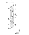
次に、図2〜図6を参照しつつ、インクジェットヘッド1について詳細に説明する。なお、図4では、アクチュエータユニット21の下方にあって破線で描くべき圧力室110、アパーチャ112及び吐出口108を実線で描いている。
Next, the inkjet head 1 will be described in detail with reference to FIGS. In FIG. 4, the
4つのインクジェットヘッド1は、いずれも同じ構造を有している。図2に示すように、インクジェットヘッド1は、流路ユニット9とアクチュエータユニット21とを含むヘッド本体2、ヘッド本体2にインクを供給するリザーバユニット71、及び電子部品が実装された制御基板54の積層体であって、制御基板54とアクチュエータユニット21とが平型柔軟基板(COF:Chip On Film)50によって電気的に接続されている。流路ユニット9上には、カバー体(サイドカバー53及びヘッドカバー55)が配置されている。流路ユニット9の上面とカバー体とが作る空間内には、アクチュエータユニット21、リザーバユニット71、COF50、制御基板54等が収納されており、外部からインクミストが侵入することがない。
All of the four inkjet heads 1 have the same structure. As shown in FIG. 2, the inkjet head 1 includes a
リザーバユニット71は、4枚のプレート91〜94が積層された流路部材であり、流路ユニット9に供給されるインクが一時的に貯留される。リザーバユニット71の内部には、外部からインクが供給されるインクリザーバ61、及び、インクリザーバ61から分岐した10個のインク流出流路62が形成されている。なお、図2においては、1つのインク流出流路62のみが表れている。プレート93には、インク溜まりであるインクリザーバ61が形成されている。また、プレート94の下面には、10個の凸部94aが形成されており、各凸部94aの先端面にはインク流出流路62が開口している。凸部94aの先端面は流路ユニット9の上面9aに接合されており、リザーバユニット71と流路ユニット9とのインク流路同士が連通している。また、プレート94の下面の凸部94aによって画定された凹部が流路ユニット9との間に空隙を作り、4つのアクチュエータユニット21がこの空隙内に配置されている。
The
COF50は、一端がアクチュエータユニット21の上面に接続され、他端が制御基板54のコネクタ54aに接続されている。COF50の途中部には、ドライバIC52が実装されている。ドライバIC52は、図2に示すように、サイドカバー53の内壁面に当接されている。本実施形態では、サイドカバー53は金属製の板材であり、ドライバIC52に対する放熱板でもある。
One end of the
次に、ヘッド本体2について説明する。ヘッド本体2は、図3に示すように、流路ユニット9と、流路ユニット9の上面9aに固定された4つのアクチュエータユニット21とを含んでいる。
Next, the
流路ユニット9は、9枚のプレート122〜130が積層された流路部材であり、リザーバユニット71のプレート94とほぼ同じサイズと形状を有している。各プレート122〜130は、主走査方向に長尺で、矩形の平面形状を有する。積層体の内部には、上面9aのインク供給口105bから下面(吐出面2a)の吐出口108に至るインク流路が形成されている。インク流路は、図3〜5に示すように、一端がインク供給口105bに連通するマニホールド流路105、マニホールド流路105から分岐した副マニホールド流路105a、副マニホールド流路105aの出口から圧力室110を介して吐出口108に至る複数の個別インク流路132からなる。図4に示すように、上面9aには、10個のインク供給口105bの他に、マトリクス状に配置された多数の圧力室110が開口している。本実施形態では、圧力室110及びインク供給口105bは、プレート122を貫通する孔やその開口として形成されている。吐出面2aには、圧力室110と同数の吐出口108がマトリクス状に開口している。
The
ここで、流路ユニット9におけるインクの流れについて説明する。リザーバユニット71からインク供給口105bを介して流路ユニット9内に供給されたインクは、マニホールド流路105から副マニホールド流路105aに分配される。副マニホールド流路105a内のインクは、各個別インク流路132に流れ込み、絞りとして機能するアパーチャ112及び圧力室110を介して吐出口108に至る。
Here, the flow of ink in the
次に、アクチュエータユニット21について説明する。図3に示すように、4つのアクチュエータユニット21は、それぞれ台形の平面形状を有しており、インク供給口105bを避けるよう主走査方向に千鳥状に配置されている。さらに、各アクチュエータユニット21の平行対向辺は主走査方向に沿っており、隣接するアクチュエータユニット21の斜辺同士は搬送方向に互いにオーバーラップしている。
Next, the
図6(a)に示すように、アクチュエータユニット21は、強誘電性を有するチタン酸ジルコン酸鉛(PZT)系のセラミックス材料からなる3枚の圧電層41〜43から構成されている。最上層の圧電層41の表面には、複数の圧力室110にそれぞれ対向して、個別電極35(焼成金属層)が形成されている。圧電層41とその下側の圧電層42との間には、シート全面に形成された共通電極34(共通電極層)が介在している。
As shown in FIG. 6A, the
個別電極35は、図6(b)に示すように、圧力室110に対向配置された主電極部35a、主電極部35aから引き出された接続部35b、及び接続部35bの先端に形成された端子形成部35cから構成されている。主電極部35aは、圧力室110とほぼ相似の形状を有し、平面視で一回り小さい略菱形である。接続部35bは、主電極部35aの一方の鋭角部から引き出され、その先端部は圧力室110と対向しない。端子形成部35cは、平面形状が円形である。本実施形態では、端子形成部35cも圧力室110と対向していない。
As shown in FIG. 6B, the
個別電極35は、Auを主成分とする導電性ペーストを焼成することによって形成される。個別電極35の材料としては、Auの他、Ag、Ag−Pdなどの金属微粒子が挙げられ、これを含有するペーストにして用いる。
The
また、各端子形成部35cと圧電層41との間には、金属層36(蒸着金属層)が形成されている。金属層36は、端子形成部35cよりも一回り大きく、平面形状は円形である。このように、圧電層41上には、金属層36と端子形成部35cとが順に積層されている。本実施の形態では、金属層36も圧力室110と対向していない。なお、金属層36は、Ti、Ni、又はCrのいずれかを蒸着材とする真空蒸着法により形成される。金属層36の形成方法としては、真空蒸着法に限らず、その他の物理蒸着法(PVD)又は化学蒸着法(CVD)を用いてもよい。
Further, a metal layer 36 (evaporated metal layer) is formed between each terminal forming
さらに、各端子形成部35c上には、ランド37が形成されている。ランド37は、端子形成部35cよりも一回り小さく、平面形状は円形である。なお、ランド37は、Ag−Pdを主成分とする導電性ペーストを焼成することによって形成される。ランド37の材料としては、Ag−Pdの他、Ag、Auなどの金属微粒子が挙げられ、これを含有するペーストにして用いる。
Furthermore, a
加えて、各ランド37上には、Agを含む金属材料からなる凸状のバンプ38が形成されている。バンプ38は、ランド37よりも一回り小さく、平面形状は円形である。外形形状は、図6(a)に示すように、半球状である。このように、圧電層41上には、金属層36、端子形成部35c、ランド37及びバンプ38がほぼ同軸上に積層されている。図6(b)に示すように、平面視で、バンプ38はランド37に包含され、ランド37は端子形成部35cに包含され、端子形成部35cは金属層36に包含されている。なお、バンプ38は、Agを主成分とする導電性ペーストを焼成することで形成される。バンプ38の材料としては、Ag以外に、Au、Ag−Pdなどの金属微粒子が挙げられ、これを含有するペーストとして用いる。
In addition, on each
バンプ38は、COF50の端子との接点である。これにより、個別電極35はバンプ38を介してドライバIC52の出力端子とそれぞれ個別に接続され、COF50の配線を通じて駆動信号が選択的に供給される。個別電極35に駆動信号が供給されると、個別電極35に対応したアクチュエータユニット21の部分は独立して変形できる。個別電極35に重なる部分は、個別のアクチュエータとして機能する。このように、アクチュエータユニット21は、一体型の駆動素子群であって、圧力室110と同数のアクチュエータが作り込まれている。
The
アクチュエータユニット21は、最上層の圧電層41だけが厚み方向に分極されている。圧電層41の個別電極35及び共通電極34で挟まれた部分(活性部)が、電界印加で変位する。活性部は、d31、d33、d15から選ばれる少なくとも1つの振動モードで変位する。本実施の形態では、活性部は、d31の振動モードで変位する。また、圧電層42、43の個別電極35に対向した部分(非活性部)は、電界を印加しても変形しない。このような組み合わせの各アクチュエータは、所謂ユニモルフタイプの圧電素子である。
In the
ここで、アクチュエータユニット21の駆動方法について説明する。共通電極34はすべての圧力室110に対応する領域において等しく基準電位が付与されるように、グランドに接続されている。これに対して、個別電極35を正又は負の所定電位にして活性部に分極方向の電界を印加すると、活性部は圧電横効果により分極方向と直交する方向(面方向)に縮む。一方、圧電層42、43は電界が印加されても自発的には変形しないので、上層の圧電層41と下層の圧電層42、43との間で面方向への歪みに差が生じる。この歪みの差によって、圧電層41〜43全体が圧力室110に向けて凸に変形しようとする(ユニモルフ変形)。
Here, a driving method of the
ここで、圧電層41〜43は圧力室110を区画するキャビティプレート122の上面に固定されているので、活性部に対応する領域(個別のアクチュエータ)が圧力室110に向かって凸になるように変形する。このとき、圧力室110の容積が低下し、圧力室110内のインクに圧力(吐出エネルギー)が付与され、吐出口108からインク滴が吐出される。その後、個別電極35を共通電極34と同じ電位に戻すと、活性部に対応する領域は元の形状になって圧力室110の容積が元の容積に戻り、マニホールド流路105から圧力室110内にインクが吸い込まれる。
Here, since the
他の駆動方法として、予め個別電極35を共通電極34と異なる電位にしておき、吐出要求がある毎に個別電極35を共通電極34と一旦同じ電位とし、その後所定の時間が経過したところで再び個別電極35を共通電極34と異なる電位にすることもできる。この場合は、初期状態において、活性部に対応する領域が圧力室110に向かって凸に変形している。吐出要求があると、個別電極35が共通電極34と同じ電位になるタイミングで、活性部に対応する領域が平坦な形状になり、圧力室110の容積が初期状態と比較して増加する。このとき、マニホールド流路105から圧力室110内にインクが吸い込まれる。その後、再び個別電極35を共通電極34と異なる電位にしたタイミングで、活性部に対応する領域が圧力室110に向かって凸に変形するので、圧力室110の容積低下によりインクへの圧力が上昇し、インクが吐出される。
As another driving method, the
次に、図7、及び図8を参照しつつ、ヘッド本体2の製造方法の一例について説明する。ヘッド本体2を製造するには、流路ユニット9とアクチュエータユニット21とを別々に作成し、その後これらを接着剤で組み付ける。アクチュエータユニット21を製造する際には、まず、積層体の圧電層41〜43を形成する。圧電層41〜43の形成に際して、圧電セラミックスの粉末を用いて所定の形状・サイズを有したグリーンシートを形成する。圧電層41のために、グリーンシートの周縁部に複数の貫通孔を形成する。圧電層42のために、グリーンシート上にスクリーン印刷で共通電極パターンを形成する。共通電極パターンは、グリーンシートの上面のほぼ全体を占める。続いて、この電極パターン付きのグリーンシートを挟むようにして、2枚のグリーンシートを積層して3枚のグリーンシートからなる圧電層41〜43の前駆体を形成する。電極パターン上には、貫通孔を持つグリーンシートが積層される。貫通孔は、共通電極パターンに対して開口している。前駆体の形成後、貫通孔内に導電性ペーストを充填する。例えば、Ag−Pd系のペーストが用いられる。そして、この前駆体を脱脂及び焼成(例えば、900〜1000℃)することで、圧電層41〜43とする。
Next, an example of a method for manufacturing the
次に、図7(a)に示すように、マスク160を用いて、真空蒸着法により金属層36を形成する。具体的には、公知の真空蒸着装置を用いて金属層36を形成する。まず、装置の真空チャンバ内に、圧電層41の表面がマスク160で覆われた焼成済み圧電層41〜43を支持し、蒸着源としてTi、Ni、又はCrのペレットを圧電層41〜43に対向してセットする。真空チャンバ内の真空度が10−3〜10−4Paに到達したところで、ペレットを抵抗加熱や電子ビーム加熱により蒸発させる。マスク160には、円形の開口161がマトリクス状に形成されている。蒸発粒子は真空チャンバ内を直線的に飛翔するので、圧電層41の上面には、金属層36が開口161と同じ平面視円形状に形成される。蒸着金属膜は、純度が高く柔軟性も高い。
Next, as shown in FIG. 7A, a
続いて、図7(b)に示すように、スクリーン印刷によって、圧電層41の表面に電極配列パターンを形成する。印刷用のマスク170には、個別電極35(主電極部35a、接続部35b、及び端子形成部35c)に対応する形状の開口171がマトリクス状に形成されている。印刷に先立ち、マスク170の端子形成部35cの部分が金属層36に包含されるように、マスク170を圧電層41〜43に位置合わせする。印刷には、Au系の導電性ペーストが用いられる。印刷の後、500〜1000℃程度で焼成する。これにより、図8(b)に示すように、マスクパターンに倣った個別電極35が形成される。個別電極35の端子形成部35cは平面視で金属層36に包含されており、接続部35bの一部及び端子形成部35cは金属層36上に重畳される。主電極部35a及び接続部35bの残りの部分は圧電層41の表面に形成される。なお、本実施形態においては、個別電極35の厚みは0.1〜1μm程度である。
Subsequently, as shown in FIG. 7B, an electrode array pattern is formed on the surface of the
さらに、図7(c)に示すように、スクリーン印刷によって、端子形成部35c上に電極配列パターンを形成する。印刷用のマスク180には、ランド37に対応する円形の開口181に加え、共通電極用のランドに対応する開口(不図示)も形成されている。ランド37対応の開口181はマトリクス状に配置され、共通電極用のランド対応の開口は、ランド37用の開口181を四方から取り囲んで配置されている。共通電極用のランド対応の開口は、台形の平行対向辺に沿って細長い。印刷に先立ち、マスク181のランド37に対応する部分が端子形成部35cに包含されるように、マスク181を圧電層41〜43に位置合わせする。このとき、共通電極用のランド対応の開口は、圧電層41の貫通孔に対向する。印刷には、Ag−Pd系のペーストが用いられる。印刷の後、500〜1000℃程度で焼成する。これにより、図8(c)に示すように、マスクパターンに倣ったランド37が形成される。ランド37は平面視で個別電極35の端子形成部35cに包含されている。図示はしないが、共通電極用のランドは、圧電層41の貫通孔内に充填されている導電体上に重畳されて、共通電極34と電気的に接続される。なお、本実施形態においては、ランド37の厚みは10μm程度である。
Further, as shown in FIG. 7C, an electrode array pattern is formed on the
さらに、図7(d)に示すように、スクリーン印刷によって、ランド37上に電極配列パターンを形成する。印刷用のマスク190には、バンプ38に対応する円形の開口191に加え、共通電極用バンプに対応する開口も形成されている。両バンプ対応の開口は、両ランド対応の開口と同様に配置されている。サイズは、各ランドの開口に比べて一回り小さい。印刷に先立ち、マスク190のバンプ38に対応する部分がランド37に包含されるように、マスク190を圧電層41〜43に位置合わせする。このとき、共通電極用バンプ対応の開口は、圧電層41の貫通孔に対向する。印刷には、Ag系の導電性ペーストが用いられる。印刷の後、100〜200℃程度で焼成する。この焼成によって、電極配列パターンが硬化する。これにより、図8(d)に示すように、マスクパターンに倣ったバンプ38が形成される。バンプ38は平面視でランド37に包含されている。なお、本実施の形態では、バンプ38の圧電層41の表面からの高さは50μm程度となっている。
Further, as shown in FIG. 7D, an electrode array pattern is formed on the
上述のように、圧電層41の表面に金属層36、個別電極35、ランド37、及びバンプ38を形成することで、アクチュエータユニット21が完成する。アクチュエータユニット21とは別に、流路ユニット9が、プレート122〜130の積層と互いの接合とにより作製される。接合には、熱硬化性接着剤が用いられる。続いて、図7(e)に示すように熱硬化性接着剤(図示せず)を介して、アクチュエータユニット21を流路ユニット9の上面9aに積層する。このとき、アクチュエータユニット21と流路ユニット9とは、各個別電極35の主電極部35aが圧力室110に対向し、各金属層36が圧力室110と対向しないように位置合わせされる。このとき、平面視で金属層36に包含される端子形成部35c、ランド37、及びバンプ38は、いずれも圧力室110と対向しない。
As described above, the
そして、治具150によって凸状のバンプ38の先端に対して金属層36に向かう圧力を加えることで、アクチュエータユニット21と流路ユニット9とを互いに近づく方向に加圧しながら加熱する。これにより、アクチュエータユニット21が流路ユニット9に固定されてヘッド本体2が完成する。
Then, by applying pressure toward the
ここで、インクジェットヘッド1を構成するリザーバユニット71、COF50、制御基板54、及びカバー体(サイドカバー53及びヘッドカバー55)は、別途それぞれの作製手順に従って用意される。
Here, the
上述のヘッド本体2に対して、COF50がアクチュエータユニット21と接合されるように取り付けられる。COF50の接合領域には、ドライバIC52の各出力端子に繋がる接合端子が配置されている。接合は、接合端子を対応するバンプ38に加圧しながら加熱(例えば、200℃程度)して行われる。このときの接合部の形態は、例えば、接合端子がバンプ38と半田で接合されていても良いし、互いに当接する接合端子とバンプ38の周囲が熱硬化性接着剤で被覆されていても良い。もちろん、これら2つを組み合わせた形態であっても良い。
The
これに続いて、リザーバユニット71がヘッド本体2に対して接合される。この接合に際して、リザーバユニット71のプレート94に形成された凸部94aが、ヘッド本体2のインク供給口105bと対向配置される。両者の接合は、間に挟んだ熱硬化性接着剤で行われる。
Subsequently, the
さらに、リザーバユニット71の上方に制御基板54を配設し、制御基板54上のコネクタ54aにCOF50の他端を繋ぐ。最後に、カバー体を流路ユニット9上に配置する。このとき、サイドカバー53は、その内壁面にドライバICが当接するように配置される。また、カバー体と流路ユニット9との境界及びカバー53、55同士の境界が、シリコンからなるポッティング剤で封止される。以上でインクジェットヘッド1が完成する。
Further, the
以上のように、本実施形態のインクジェットヘッド1に備えられたアクチュエータユニット21では、圧電層41の表面に焼成によって形成された個別電極35と、個別電極35と電気的に接続され且つ圧電層41との間に個別電極35を挟むように焼成によって形成された金属端子であるバンプ38と、圧電層41とバンプ38との間に蒸着によって形成された金属層36とを備えている。したがって、クラックが発生しても、金属層36を境にその伝搬を抑制することができる。よって、圧電層41とバンプ38とに跨るクラックが発生するのを抑制することができる。その結果、バンプ38に安価な銀系材料を採用したとしても、バンプ38を構成する銀元素のマイグレーションに伴うアクチュエータユニット21の絶縁劣化が発生する確率を低下させることができる。
As described above, in the
また、本実施形態のインクジェットヘッド1では、平面視でバンプ38は金属層36に包含されている。したがって、バンプ38が金属層36を介さずに圧電層41と接触することがなくなるので、圧電層41とバンプ38とに跨るクラックが発生するのをより確実に抑制することができる。
In the inkjet head 1 of the present embodiment, the
また、本実施形態のインクジェットヘッド1では、平面視でバンプ38は個別電極35に包含されている。したがって、個別電極35が緩衝材となって圧電層41とバンプ38とに跨るクラックが発生するのをさらに抑制することができる。
In the inkjet head 1 of the present embodiment, the
さらに、本実施形態のインクジェットヘッド1では、バンプ38と個別電極35との間に金属層であるランド37が焼成により形成されており、平面視でバンプ38がランド37に包含されており、且つランド37が金属層36に包含されている。したがって、ランド37を起点として圧電層41に達するクラックが発生するのを金属層36によって抑制することができる。
Furthermore, in the inkjet head 1 of the present embodiment, lands 37 that are metal layers are formed by firing between the
加えて、本実施形態のインクジェットヘッド1では、金属層36がTi、Ni、又はCrのいずれかからなる。したがって、金属層36によるクラックの伝搬抑制効果を高めることができる。
In addition, in the inkjet head 1 of the present embodiment, the
さらに、本実施形態のインクジェットヘッド1では、圧電層41の表面上に複数の個別電極35が形成されており、これら複数の個別電極35のそれぞれについてバンプ38及び金属層36が設けられている。また、複数の個別電極35と圧電層41を挟んで対向する共通電極34を備えている。したがって、クラックの発生しやすい大型の圧電層について、クラックが発生しても金属層36を境にその伝搬を抑制し、圧電層41とバンプ38とに跨るクラックが発生するのを抑制することができる。
Furthermore, in the inkjet head 1 of the present embodiment, a plurality of
また、本実施形態のインクジェットヘッド1では、複数の金属層36が複数の圧力室110と対向していない。したがって、インクを吐出させる際の圧電層41〜43における圧力室110に対向する部分の変形が、金属層36によって阻害されることがほとんどなくなる。
In the inkjet head 1 of the present embodiment, the plurality of
以上、本発明の好適な一実施形態について説明したが、本発明は上述の実施の形態に限られるものではなく、特許請求の範囲に記載した限りにおいて、様々な設計変更を行うことが可能なものである。 The preferred embodiment of the present invention has been described above. However, the present invention is not limited to the above-described embodiment, and various design changes can be made as long as they are described in the claims. Is.
例えば、上述の実施形態では、圧電層41の表面に金属層36が形成されており、金属層36上に個別電極35の接続部35bの一部及び端子形成部35cが重畳されている場合について説明したがこれには限定されない。すなわち、金属層36は圧電層41とバンプ38との間に形成されていればよく、個別電極35と金属層36との上下関係が逆転し、個別電極35全体が圧電層41の表面に形成されており、個別電極の端子形成部35c上に金属層36が重畳されていてもよい。
For example, in the above-described embodiment, the
さらに、上述の実施形態では、平面視でバンプ38が個別電極35及び金属層36に包含されている場合について説明したがこれには限定されない。バンプ38は、個別電極35に包含されておらず、金属層36のみに包含されていてもよい。
Furthermore, although the above-mentioned embodiment demonstrated the case where the
加えて、上述の実施形態では、平面視でバンプ38がランド37に包含されており且つランド37が金属層36に包含されている場合について説明したが、ランド37が形成されていなくてもよい。
In addition, in the above-described embodiment, the case where the
また、上述の実施形態では、金属層36がTi、Ni、又はCrのいずれかからなる場合について説明したが、金属層36は蒸着によって形成されるものであれば、上記以外の金属物質からなるものであってもよい。
Moreover, although the case where the
また、上述の実施形態では、アクチュエータユニット21は、1層が活性層を含み、全体で3層の圧電層からなる積層体として説明したが、例えば、圧電層43を含まない2層からなる積層体であっても良い。あるいは、アクチュエータユニット21は、4層以上の多層からなる積層体であっても良い。この場合、活性層を含む層が複数層あっても良い。
In the above-described embodiment, the
また、上述の実施形態では、本発明を吐出口108からインクを吐出するインクジェットヘッド1に適用した例について説明したが、インク以外の液体を吐出する液体吐出ヘッドに本発明を適用することも可能である。さらには、種々の装置の駆動部を駆動するための圧電アクチュエータに本発明を適用することも可能である。
In the above-described embodiment, the example in which the present invention is applied to the inkjet head 1 that ejects ink from the
2 ヘッド本体(液体吐出ヘッド)
9 流路ユニット
21 アクチュエータユニット(圧電アクチュエータ)
35 個別電極(焼成電極層)
36 金属層(蒸着金属層)
37 ランド(焼成金属層)
38 バンプ(焼成金属端子)
41〜43 圧電層
34 共通電極(共通電極層)
108 吐出口
110 圧力室
132 個別インク流路(個別液体流路)
2 Head body (liquid discharge head)
9
35 Individual electrode (firing electrode layer)
36 Metal layer (vapor deposition metal layer)
37 land (fired metal layer)
38 Bump (fired metal terminal)
41 to 43
108
Claims (17)
前記一表面に積層される圧電層と、
前記圧電層が前記一表面に積層されたとき前記圧力室のそれぞれと対向する位置に、前記圧電層の表面上に焼成によって前記圧力室毎に形成された複数の焼成電極層と、
前記圧電層が前記一表面に積層されたとき前記圧力室と対向しない位置に、前記複数の焼成電極層のそれぞれと電気的に接続され且つ前記圧電層との間に前記焼成電極層を挟むように焼成によって形成された、外部端子との接点となる複数の焼成金属端子と、
前記圧電層が前記一表面に積層されたとき前記圧力室と対向しない位置に、前記圧電層と前記焼成金属端子との間に蒸着によって前記焼成金属端子毎に形成された複数の蒸着金属層とを備えていることを特徴とする圧電アクチュエータ。 A flow path unit in which a plurality of individual liquid flow paths each including a discharge port for discharging a liquid and a pressure chamber communicating with the discharge port are formed, and laminated on one surface of the flow path unit, and the liquid in the pressure chamber A piezoelectric actuator used in a liquid discharge head having a piezoelectric actuator that applies discharge energy from the discharge port,
A piezoelectric layer laminated on the one surface ;
A plurality of fired electrode layers formed for each of the pressure chambers by firing on the surface of the piezoelectric layer at positions facing each of the pressure chambers when the piezoelectric layer is laminated on the one surface ;
When the piezoelectric layer is laminated on the one surface, it is electrically connected to each of the plurality of fired electrode layers at a position not facing the pressure chamber, and the fired electrode layer is sandwiched between the piezoelectric layers. A plurality of fired metal terminals, which are formed by firing, and serve as contact points with external terminals;
A plurality of vapor-deposited metal layers formed for each of the fired metal terminals by vapor deposition between the piezoelectric layer and the fired metal terminals at a position not facing the pressure chamber when the piezoelectric layer is laminated on the one surface ; A piezoelectric actuator comprising:
前記表面と直交する方向から見て、前記焼成金属端子が前記焼成金属層に包含されており且つ前記焼成金属層が前記蒸着金属層に包含されていることを特徴とする請求項1〜4のいずれか1項に記載の圧電アクチュエータ。 A fired metal layer is formed by firing between the fired metal terminal and the fired electrode layer,
When viewed from a direction perpendicular to the surface, the metal terminal is of the preceding claims, wherein the sintered metal layer on the inclusion has been provided and the firing metal layer is characterized in that it is included in the deposited metal layer The piezoelectric actuator according to any one of claims.
前記蒸着金属層、前記端子形成部、前記焼成金属層、及び前記焼成金属端子が、前記表面と直交する方向から見て円形形状を有すると共に、前記圧電層の上に同軸上に積層されており、The vapor-deposited metal layer, the terminal forming portion, the fired metal layer, and the fired metal terminal have a circular shape when viewed from a direction orthogonal to the surface, and are coaxially stacked on the piezoelectric layer. ,
前記焼成金属端子が、銀を主成分とするペーストを焼成することで形成されていることを特徴とする請求項5に記載の圧電アクチュエータ。6. The piezoelectric actuator according to claim 5, wherein the fired metal terminal is formed by firing a paste containing silver as a main component.
前記複数の焼成電極層が複数の前記圧力室のそれぞれと対向し、前記複数の焼成電極層のそれぞれと電気的に接続された前記複数の焼成金属端子及び前記複数の蒸着金属層が前記流路ユニットの前記圧力室以外の部分と対向すると共に、前記複数の焼成金属端子が前記流路ユニットとは反対方向に突出するように、前記流路ユニットに取り付けられた請求項8に記載の圧電アクチュエータとを備えていることを特徴とする液体吐出ヘッド。 A flow path unit in which a plurality of individual liquid flow paths each including a discharge port for discharging a liquid and a pressure chamber communicating with the discharge port are formed;
Said plurality of firing electrode layer is opposed to each of the plurality of the pressure chambers, respectively electrically connected to said plurality of metal terminal and said plurality of vapor Chakukinzoku layer said flow of said plurality of firing electrode layer with portions facing other than the pressure chamber of the road unit, the plurality of baked formation metal terminal as the the channel unit to protrude in the opposite directions, according to claim 8 which is attached to the channel unit A liquid discharge head comprising a piezoelectric actuator.
前記一表面に積層される圧電層を焼成によって形成する工程と、
前記圧電層が前記一表面に積層されたとき前記圧力室のそれぞれと対向しない位置に、前記圧電層の表面上に複数の蒸着金属層を蒸着によって前記圧力室毎に形成する工程と、
前記圧電層が前記一表面に積層されたとき前記圧力室のそれぞれと対向する位置に、前記圧電層の前記表面上に複数の焼成電極層を焼成によって前記圧力室毎に形成する工程と、
前記圧電層が前記一表面に積層されたとき前記圧力室のそれぞれと対向しない位置に、前記蒸着金属層上に、前記複数の焼成電極層のそれぞれと電気的に接続され且つ前記圧電層との間に前記焼成電極層を挟むように、外部端子との接点となる複数の焼成金属端子を焼成によって形成する工程とを備えていることを特徴とする圧電アクチュエータの製造方法。 A flow path unit in which a plurality of individual liquid flow paths each including a discharge port for discharging a liquid and a pressure chamber communicating with the discharge port are formed, and laminated on one surface of the flow path unit, and the liquid in the pressure chamber A method of manufacturing a piezoelectric actuator for use in a liquid discharge head having a piezoelectric actuator that applies discharge energy from the discharge port,
Forming a piezoelectric layer laminated on the one surface by firing;
Forming a plurality of vapor-deposited metal layers for each of the pressure chambers by vapor deposition on the surface of the piezoelectric layer at positions not facing each of the pressure chambers when the piezoelectric layer is laminated on the one surface ;
Forming for each of the pressure chamber at a position opposed to each of the pressure chamber when the piezoelectric layer is laminated on the one surface, by firing a plurality of firing electrode layer on the surface of the piezoelectric layer,
The piezoelectric layer is electrically connected to each of the plurality of fired electrode layers on the vapor-deposited metal layer at a position that does not face each of the pressure chambers when the piezoelectric layer is laminated on the one surface and the piezoelectric layer. And a step of forming a plurality of fired metal terminals serving as contacts with external terminals by firing so as to sandwich the fired electrode layer therebetween.
前記蒸着金属層を形成する工程において、前記圧電層と前記焼成電極層とに挟まれるように、前記蒸着金属層を形成することを特徴とする請求項11〜13のいずれか1項に記載の圧電アクチュエータの製造方法。The process of forming the said vapor deposition metal layer WHEREIN: The said vapor deposition metal layer is formed so that it may be pinched | interposed between the said piezoelectric layer and the said baking electrode layer, The any one of Claims 11-13 characterized by the above-mentioned. A method for manufacturing a piezoelectric actuator.
前記焼成金属層を形成する工程において、前記表面と直交する方向から見て、前記焼成金属端子を包含すると共に前記蒸着金属層に包含されるように前記焼成金属層を形成することを特徴とする請求項11〜14のいずれか1項に記載の圧電アクチュエータの製造方法。 A step of forming a fired metal layer by firing between the step of forming the fired electrode layer and the step of forming the fired metal terminal;
In the step of forming the fired metal layer, the fired metal layer is formed so as to include the fired metal terminal and to be included in the vapor-deposited metal layer when viewed from a direction orthogonal to the surface. The manufacturing method of the piezoelectric actuator of any one of Claims 11-14 .
前記焼成金属端子を形成する工程において、銀を主成分とするペーストを焼成することで、前記焼成金属端子を形成することを特徴とする請求項11〜15のいずれか1項に記載の圧電アクチュエータの製造方法。The piezoelectric actuator according to claim 11, wherein in the step of forming the fired metal terminal, the fired metal terminal is formed by firing a paste mainly composed of silver. Manufacturing method.
前記圧電アクチュエータを前記流路ユニットの前記一表面に積層したときに前記一表面に積層される圧電層の表面上に前記圧力室のそれぞれに対応する複数の蒸着金属層を蒸着によって形成する工程、前記圧電層の前記表面上に前記圧力室のそれぞれに対応する複数の焼成電極層を焼成によって形成する工程、及び前記蒸着金属層上に外部端子との接点となる凸状の複数の焼成金属端子を焼成によって形成する工程を含む前記圧電アクチュエータを形成する工程と、
塗布された熱硬化性接着剤を介して、前記複数の焼成電極層が前記圧力室のそれぞれと対向し、前記複数の蒸着金属層が前記流路ユニットの前記圧力室以外の部分と対向し、且つ、前記複数の焼成金属端子が前記流路ユニットの前記圧力室以外の部分と対向するように、前記圧電アクチュエータを前記流路ユニットの前記一表面に積層する工程と、
前記圧電アクチュエータと前記流路ユニットとを互いに近づく方向に加圧しながら加熱して、前記圧電アクチュエータを前記流路ユニットに固定する工程とを備え、
前記焼成金属端子の形成工程において、
前記焼成金属端子が前記圧電層との間に前記焼成電極層を挟むとともに、前記圧電層の前記表面と直交する方向から見たときに、前記焼成金属端子が前記蒸着金属層に包含されるように前記焼成金属端子を形成するとともに、
前記圧電アクチュエータを前記流路ユニットに固定する工程において、
凸状の前記焼成金属端子の先端に対して、前記蒸着金属層に向かう圧力を加えることを特徴とする液体吐出ヘッドの製造方法。
A flow path unit in which a plurality of individual liquid flow paths each including a discharge port from which liquid is discharged and a pressure chamber formed on one surface are formed, and the liquid in the pressure chamber is stacked on one surface of the flow path unit. In a method of manufacturing a liquid discharge head having a piezoelectric actuator for applying discharge energy from the discharge port to
Forming a plurality of vapor deposition metal layers corresponding to each of the pressure chambers by vapor deposition on the surface of the piezoelectric layer laminated on the one surface when the piezoelectric actuator is laminated on the one surface of the flow path unit ; Forming a plurality of fired electrode layers corresponding to each of the pressure chambers on the surface of the piezoelectric layer by firing; and a plurality of convex fired metal terminals serving as contact points with external terminals on the deposited metal layer Forming the piezoelectric actuator including a step of forming the substrate by firing;
Through the applied thermosetting adhesive , the plurality of fired electrode layers face each of the pressure chambers, the plurality of deposited metal layers face a portion other than the pressure chambers of the flow path unit, and such that said plurality of metal terminal is part facing other than the pressure chamber of the flow path unit, a step of laminating the piezoelectric actuator on the one surface of the flow path unit,
Heating while pressing the piezoelectric actuator and the flow path unit in a direction approaching each other, and fixing the piezoelectric actuator to the flow path unit,
In the step of forming the fired metal terminal,
The fired metal terminal sandwiches the fired electrode layer between the piezoelectric layer and the fired metal terminal is included in the deposited metal layer when viewed from a direction orthogonal to the surface of the piezoelectric layer. And forming the fired metal terminal in
In the step of fixing the piezoelectric actuator to the flow path unit,
A method of manufacturing a liquid discharge head, comprising applying a pressure toward the vapor-deposited metal layer to the tip of the convex fired metal terminal.
Priority Applications (4)
| Application Number | Priority Date | Filing Date | Title |
|---|---|---|---|
| JP2009271391A JP5126208B2 (en) | 2009-11-30 | 2009-11-30 | Piezoelectric actuator, liquid discharge head, method for manufacturing piezoelectric actuator, and method for manufacturing liquid discharge head |
| EP10010214.4A EP2327551B1 (en) | 2009-11-30 | 2010-09-22 | Piezoelectric actuator, liquid discharge head and method of manufacturing same |
| US12/891,850 US8613500B2 (en) | 2009-11-30 | 2010-09-28 | Piezoelectric actuator, liquid discharge head, and method of manufacturing same |
| CN201010505366.6A CN102079168B (en) | 2009-11-30 | 2010-09-29 | Piezoelectric actuator, liquid discharge head and method of manufacturing same |
Applications Claiming Priority (1)
| Application Number | Priority Date | Filing Date | Title |
|---|---|---|---|
| JP2009271391A JP5126208B2 (en) | 2009-11-30 | 2009-11-30 | Piezoelectric actuator, liquid discharge head, method for manufacturing piezoelectric actuator, and method for manufacturing liquid discharge head |
Publications (2)
| Publication Number | Publication Date |
|---|---|
| JP2011110892A JP2011110892A (en) | 2011-06-09 |
| JP5126208B2 true JP5126208B2 (en) | 2013-01-23 |
Family
ID=43221975
Family Applications (1)
| Application Number | Title | Priority Date | Filing Date |
|---|---|---|---|
| JP2009271391A Active JP5126208B2 (en) | 2009-11-30 | 2009-11-30 | Piezoelectric actuator, liquid discharge head, method for manufacturing piezoelectric actuator, and method for manufacturing liquid discharge head |
Country Status (4)
| Country | Link |
|---|---|
| US (1) | US8613500B2 (en) |
| EP (1) | EP2327551B1 (en) |
| JP (1) | JP5126208B2 (en) |
| CN (1) | CN102079168B (en) |
Families Citing this family (7)
| Publication number | Priority date | Publication date | Assignee | Title |
|---|---|---|---|---|
| US8593016B2 (en) * | 2010-12-03 | 2013-11-26 | Sri International | Levitated micro-manipulator system |
| JP5957914B2 (en) * | 2012-02-01 | 2016-07-27 | セイコーエプソン株式会社 | Liquid ejecting head and liquid ejecting apparatus |
| US8888254B2 (en) | 2012-09-13 | 2014-11-18 | Xerox Corporation | High density three-dimensional electrical interconnections |
| JP6191983B2 (en) * | 2013-06-11 | 2017-09-06 | ブラザー工業株式会社 | Piezoelectric actuator manufacturing method, piezoelectric actuator, and liquid ejection device |
| CN105848905B (en) * | 2013-12-25 | 2017-09-19 | 京瓷株式会社 | Piezoelectric substrate, component using same, liquid ejection head and recording device |
| US10861627B2 (en) | 2015-04-20 | 2020-12-08 | Sri International | Microrobot and microrobotic train self-assembly with end-effectors |
| JP2020151890A (en) * | 2019-03-19 | 2020-09-24 | 東芝ホクト電子株式会社 | Thermal print head and thermal printer |
Family Cites Families (15)
| Publication number | Priority date | Publication date | Assignee | Title |
|---|---|---|---|---|
| JPH0496286A (en) * | 1990-08-03 | 1992-03-27 | Toyota Motor Corp | Manufacture of laminated piezoelectric element |
| JP3728931B2 (en) | 1997-06-17 | 2005-12-21 | セイコーエプソン株式会社 | Inkjet recording head |
| JP4362996B2 (en) * | 2001-08-22 | 2009-11-11 | 富士ゼロックス株式会社 | Piezoelectric / electrostrictive actuator having lattice arrangement and manufacturing method thereof |
| JP3687601B2 (en) | 2001-12-07 | 2005-08-24 | 株式会社村田製作所 | ELECTRONIC COMPONENT ELEMENT, ITS MANUFACTURING METHOD, AND ELECTRONIC COMPONENT DEVICE |
| JP3903893B2 (en) * | 2002-09-24 | 2007-04-11 | ブラザー工業株式会社 | Inkjet head |
| JP4161213B2 (en) * | 2004-01-23 | 2008-10-08 | ブラザー工業株式会社 | Wiring board bonding structure in ink jet recording head and bonding method thereof |
| JP4525094B2 (en) * | 2004-01-30 | 2010-08-18 | ブラザー工業株式会社 | Inkjet head manufacturing method |
| JP4243850B2 (en) * | 2004-05-11 | 2009-03-25 | ブラザー工業株式会社 | Multilayer piezoelectric element and ink jet recording head including the same |
| JP2007012825A (en) * | 2005-06-29 | 2007-01-18 | Ricoh Co Ltd | Chip part and its manufacturing method |
| JP4296441B2 (en) | 2006-10-11 | 2009-07-15 | セイコーエプソン株式会社 | Method for manufacturing actuator device |
| JP4407725B2 (en) * | 2007-06-29 | 2010-02-03 | ブラザー工業株式会社 | Liquid discharge head |
| JP5007823B2 (en) * | 2008-02-25 | 2012-08-22 | セイコーエプソン株式会社 | Method for manufacturing liquid jet head |
| JP2009255529A (en) | 2008-03-27 | 2009-11-05 | Seiko Epson Corp | Liquid ejecting head, liquid ejecting apparatus and actuator |
| CN101544113A (en) | 2008-03-27 | 2009-09-30 | 精工爱普生株式会社 | Liquid ejecting head, liquid ejecting apparatus, and actuator |
| JP4618368B2 (en) | 2008-12-01 | 2011-01-26 | ブラザー工業株式会社 | Recording head manufacturing method and recording head |
-
2009
- 2009-11-30 JP JP2009271391A patent/JP5126208B2/en active Active
-
2010
- 2010-09-22 EP EP10010214.4A patent/EP2327551B1/en active Active
- 2010-09-28 US US12/891,850 patent/US8613500B2/en active Active
- 2010-09-29 CN CN201010505366.6A patent/CN102079168B/en active Active
Also Published As
| Publication number | Publication date |
|---|---|
| CN102079168B (en) | 2015-07-08 |
| US8613500B2 (en) | 2013-12-24 |
| EP2327551B1 (en) | 2015-10-21 |
| US20110128328A1 (en) | 2011-06-02 |
| CN102079168A (en) | 2011-06-01 |
| EP2327551A1 (en) | 2011-06-01 |
| JP2011110892A (en) | 2011-06-09 |
Similar Documents
| Publication | Publication Date | Title |
|---|---|---|
| JP5126208B2 (en) | Piezoelectric actuator, liquid discharge head, method for manufacturing piezoelectric actuator, and method for manufacturing liquid discharge head | |
| JP2004136663A (en) | Ink jet head and method of manufacturing the same | |
| JP5197893B2 (en) | Piezoelectric actuator, liquid discharge head, and recording apparatus | |
| JP5952310B2 (en) | Liquid discharge head and recording apparatus using the same | |
| JP3951933B2 (en) | Ink jet head and ink jet printer having the same | |
| WO2003070470A1 (en) | Ink jet head and ink jet printer | |
| CN1442295A (en) | Ink jet printer head and ink jet printer having said ink jet printer head | |
| JP5997219B2 (en) | Piezoelectric actuator substrate, liquid ejection head using the same, and recording apparatus | |
| JP2011167875A (en) | Piezoelectric actuator and method of manufacturing the same | |
| JP5434932B2 (en) | Liquid discharge head and manufacturing method thereof | |
| EP1403052B1 (en) | Inkjet head | |
| JP2011054593A (en) | Method for manufacturing piezoelectric actuator and method for manufacturing liquid transfer apparatus | |
| JP2012106386A (en) | Liquid jet head and manufacturing method thereof | |
| JP6034157B2 (en) | LIQUID DISCHARGE HEAD, RECORDING DEVICE USING THE SAME, AND PIEZOELECTRIC ACTUATOR BOARD USED FOR THE SAME | |
| JP6059394B2 (en) | Piezoelectric actuator substrate, liquid ejection head using the same, and recording apparatus | |
| JP2004160966A (en) | INK JET HEAD AND METHOD FOR MANUFACTURING THE SAME, INK JET PRINTER, AND METHOD FOR MANUFACTURING ACTUATOR UNIT | |
| JP2004160967A (en) | Ink jet head and ink jet printer | |
| JP2012056288A (en) | Liquid ejection head and method for manufacturing the same | |
| JP6039365B2 (en) | Liquid discharge head and recording apparatus using the same | |
| JP6075777B2 (en) | Piezoelectric actuator substrate, liquid ejection head using the same, and recording apparatus | |
| JP6166118B2 (en) | Piezoelectric actuator substrate, liquid ejection head using the same, and recording apparatus | |
| JP2014104646A (en) | Liquid discharge head and recording device using the same | |
| JP5076512B2 (en) | Droplet discharge device | |
| JP5977031B2 (en) | Liquid discharge head and recording apparatus using the same | |
| JP5762046B2 (en) | Piezoelectric actuator unit, liquid discharge head using the same, and recording apparatus |
Legal Events
| Date | Code | Title | Description |
|---|---|---|---|
| A621 | Written request for application examination |
Free format text: JAPANESE INTERMEDIATE CODE: A621 Effective date: 20110325 |
|
| A977 | Report on retrieval |
Free format text: JAPANESE INTERMEDIATE CODE: A971007 Effective date: 20111019 |
|
| A131 | Notification of reasons for refusal |
Free format text: JAPANESE INTERMEDIATE CODE: A131 Effective date: 20111206 |
|
| A521 | Request for written amendment filed |
Free format text: JAPANESE INTERMEDIATE CODE: A523 Effective date: 20120131 |
|
| A131 | Notification of reasons for refusal |
Free format text: JAPANESE INTERMEDIATE CODE: A131 Effective date: 20120815 |
|
| TRDD | Decision of grant or rejection written | ||
| A01 | Written decision to grant a patent or to grant a registration (utility model) |
Free format text: JAPANESE INTERMEDIATE CODE: A01 Effective date: 20121002 |
|
| A01 | Written decision to grant a patent or to grant a registration (utility model) |
Free format text: JAPANESE INTERMEDIATE CODE: A01 |
|
| A61 | First payment of annual fees (during grant procedure) |
Free format text: JAPANESE INTERMEDIATE CODE: A61 Effective date: 20121015 |
|
| R150 | Certificate of patent or registration of utility model |
Ref document number: 5126208 Country of ref document: JP Free format text: JAPANESE INTERMEDIATE CODE: R150 Free format text: JAPANESE INTERMEDIATE CODE: R150 |
|
| FPAY | Renewal fee payment (event date is renewal date of database) |
Free format text: PAYMENT UNTIL: 20151109 Year of fee payment: 3 |