JP5086959B2 - Nonvolatile semiconductor memory device - Google Patents
Nonvolatile semiconductor memory device Download PDFInfo
- Publication number
- JP5086959B2 JP5086959B2 JP2008248350A JP2008248350A JP5086959B2 JP 5086959 B2 JP5086959 B2 JP 5086959B2 JP 2008248350 A JP2008248350 A JP 2008248350A JP 2008248350 A JP2008248350 A JP 2008248350A JP 5086959 B2 JP5086959 B2 JP 5086959B2
- Authority
- JP
- Japan
- Prior art keywords
- layer
- memory
- conductive layer
- transistor
- word line
- Prior art date
- Legal status (The legal status is an assumption and is not a legal conclusion. Google has not performed a legal analysis and makes no representation as to the accuracy of the status listed.)
- Active
Links
- 239000004065 semiconductor Substances 0.000 title claims description 293
- 230000015654 memory Effects 0.000 claims description 314
- 239000000758 substrate Substances 0.000 claims description 35
- 239000010410 layer Substances 0.000 description 602
- 230000006870 function Effects 0.000 description 34
- 101000578349 Homo sapiens Nucleolar MIF4G domain-containing protein 1 Proteins 0.000 description 21
- 102100027969 Nucleolar MIF4G domain-containing protein 1 Human genes 0.000 description 21
- 238000006243 chemical reaction Methods 0.000 description 20
- 238000010586 diagram Methods 0.000 description 13
- 239000011159 matrix material Substances 0.000 description 13
- 230000002093 peripheral effect Effects 0.000 description 11
- 101000927268 Hyas araneus Arasin 1 Proteins 0.000 description 10
- 230000000694 effects Effects 0.000 description 10
- 229910021420 polycrystalline silicon Inorganic materials 0.000 description 7
- 229920005591 polysilicon Polymers 0.000 description 7
- 229910052581 Si3N4 Inorganic materials 0.000 description 6
- 229910004298 SiO 2 Inorganic materials 0.000 description 6
- VYPSYNLAJGMNEJ-UHFFFAOYSA-N Silicium dioxide Chemical compound O=[Si]=O VYPSYNLAJGMNEJ-UHFFFAOYSA-N 0.000 description 6
- HQVNEWCFYHHQES-UHFFFAOYSA-N silicon nitride Chemical compound N12[Si]34N5[Si]62N3[Si]51N64 HQVNEWCFYHHQES-UHFFFAOYSA-N 0.000 description 6
- 229910052814 silicon oxide Inorganic materials 0.000 description 6
- 101100301219 Arabidopsis thaliana RDR6 gene Proteins 0.000 description 5
- 101100292586 Caenorhabditis elegans mtr-4 gene Proteins 0.000 description 5
- 102100038712 Cap-specific mRNA (nucleoside-2'-O-)-methyltransferase 1 Human genes 0.000 description 5
- 101710203121 Cap-specific mRNA (nucleoside-2'-O-)-methyltransferase 1 Proteins 0.000 description 5
- 102100038716 Cap-specific mRNA (nucleoside-2'-O-)-methyltransferase 2 Human genes 0.000 description 5
- 101710203126 Cap-specific mRNA (nucleoside-2'-O-)-methyltransferase 2 Proteins 0.000 description 5
- 101000927265 Hyas araneus Arasin 2 Proteins 0.000 description 5
- 239000011229 interlayer Substances 0.000 description 5
- 101100186130 Arabidopsis thaliana NAC052 gene Proteins 0.000 description 4
- 101100529509 Arabidopsis thaliana RECQL4A gene Proteins 0.000 description 4
- 101100203168 Saccharomyces cerevisiae (strain ATCC 204508 / S288c) SGS1 gene Proteins 0.000 description 4
- 238000000034 method Methods 0.000 description 4
- 101100365384 Mus musculus Eefsec gene Proteins 0.000 description 3
- 238000003491 array Methods 0.000 description 3
- 239000003990 capacitor Substances 0.000 description 2
- 238000009792 diffusion process Methods 0.000 description 2
- 210000000707 wrist Anatomy 0.000 description 2
- 238000007792 addition Methods 0.000 description 1
- 238000007599 discharging Methods 0.000 description 1
- 238000009413 insulation Methods 0.000 description 1
- 238000012986 modification Methods 0.000 description 1
- 230000004048 modification Effects 0.000 description 1
- 230000000149 penetrating effect Effects 0.000 description 1
- 238000006467 substitution reaction Methods 0.000 description 1
Images


Classifications
-
- H—ELECTRICITY
- H10—SEMICONDUCTOR DEVICES; ELECTRIC SOLID-STATE DEVICES NOT OTHERWISE PROVIDED FOR
- H10B—ELECTRONIC MEMORY DEVICES
- H10B43/00—EEPROM devices comprising charge-trapping gate insulators
- H10B43/20—EEPROM devices comprising charge-trapping gate insulators characterised by three-dimensional arrangements, e.g. with cells on different height levels
- H10B43/23—EEPROM devices comprising charge-trapping gate insulators characterised by three-dimensional arrangements, e.g. with cells on different height levels with source and drain on different levels, e.g. with sloping channels
- H10B43/27—EEPROM devices comprising charge-trapping gate insulators characterised by three-dimensional arrangements, e.g. with cells on different height levels with source and drain on different levels, e.g. with sloping channels the channels comprising vertical portions, e.g. U-shaped channels
-
- G—PHYSICS
- G11—INFORMATION STORAGE
- G11C—STATIC STORES
- G11C16/00—Erasable programmable read-only memories
- G11C16/02—Erasable programmable read-only memories electrically programmable
- G11C16/04—Erasable programmable read-only memories electrically programmable using variable threshold transistors, e.g. FAMOS
- G11C16/0483—Erasable programmable read-only memories electrically programmable using variable threshold transistors, e.g. FAMOS comprising cells having several storage transistors connected in series
-
- G—PHYSICS
- G11—INFORMATION STORAGE
- G11C—STATIC STORES
- G11C16/00—Erasable programmable read-only memories
- G11C16/02—Erasable programmable read-only memories electrically programmable
- G11C16/06—Auxiliary circuits, e.g. for writing into memory
- G11C16/08—Address circuits; Decoders; Word-line control circuits
-
- G—PHYSICS
- G11—INFORMATION STORAGE
- G11C—STATIC STORES
- G11C16/00—Erasable programmable read-only memories
- G11C16/02—Erasable programmable read-only memories electrically programmable
- G11C16/06—Auxiliary circuits, e.g. for writing into memory
- G11C16/30—Power supply circuits
-
- G—PHYSICS
- G11—INFORMATION STORAGE
- G11C—STATIC STORES
- G11C5/00—Details of stores covered by group G11C11/00
- G11C5/02—Disposition of storage elements, e.g. in the form of a matrix array
-
- H—ELECTRICITY
- H10—SEMICONDUCTOR DEVICES; ELECTRIC SOLID-STATE DEVICES NOT OTHERWISE PROVIDED FOR
- H10B—ELECTRONIC MEMORY DEVICES
- H10B43/00—EEPROM devices comprising charge-trapping gate insulators
- H10B43/10—EEPROM devices comprising charge-trapping gate insulators characterised by the top-view layout
-
- H—ELECTRICITY
- H10—SEMICONDUCTOR DEVICES; ELECTRIC SOLID-STATE DEVICES NOT OTHERWISE PROVIDED FOR
- H10B—ELECTRONIC MEMORY DEVICES
- H10B43/00—EEPROM devices comprising charge-trapping gate insulators
- H10B43/30—EEPROM devices comprising charge-trapping gate insulators characterised by the memory core region
- H10B43/35—EEPROM devices comprising charge-trapping gate insulators characterised by the memory core region with cell select transistors, e.g. NAND
-
- H—ELECTRICITY
- H10—SEMICONDUCTOR DEVICES; ELECTRIC SOLID-STATE DEVICES NOT OTHERWISE PROVIDED FOR
- H10B—ELECTRONIC MEMORY DEVICES
- H10B43/00—EEPROM devices comprising charge-trapping gate insulators
- H10B43/40—EEPROM devices comprising charge-trapping gate insulators characterised by the peripheral circuit region
-
- H—ELECTRICITY
- H10—SEMICONDUCTOR DEVICES; ELECTRIC SOLID-STATE DEVICES NOT OTHERWISE PROVIDED FOR
- H10D—INORGANIC ELECTRIC SEMICONDUCTOR DEVICES
- H10D30/00—Field-effect transistors [FET]
- H10D30/60—Insulated-gate field-effect transistors [IGFET]
- H10D30/69—IGFETs having charge trapping gate insulators, e.g. MNOS transistors
- H10D30/693—Vertical IGFETs having charge trapping gate insulators
-
- H—ELECTRICITY
- H10—SEMICONDUCTOR DEVICES; ELECTRIC SOLID-STATE DEVICES NOT OTHERWISE PROVIDED FOR
- H10D—INORGANIC ELECTRIC SEMICONDUCTOR DEVICES
- H10D88/00—Three-dimensional [3D] integrated devices
Landscapes
- Engineering & Computer Science (AREA)
- Microelectronics & Electronic Packaging (AREA)
- Non-Volatile Memory (AREA)
- Semiconductor Memories (AREA)
- Read Only Memory (AREA)
Description
本発明は、電気的にデータの書き換えが可能な不揮発性半導体記憶装置に関する。 The present invention relates to a nonvolatile semiconductor memory device capable of electrically rewriting data.
NAND型フラッシュメモリのビット密度向上にあっては、微細化技術が限界に近づいてきたことから、メモリセルの積層化が期待されている。そのひとつとして、縦型トランジスタを用いてメモリセルを構成した積層型のNAND型フラッシュメモリが提案されている(例えば、特許文献1参照)。ここで、特許文献1に記載の技術を用いた場合、積層するほどコンタクトゲート(CG)の数や、選択ゲート(SG)の数が増え、周辺回路面積は増大してしまう。
In order to improve the bit density of the NAND flash memory, the miniaturization technique has approached the limit, and therefore, it is expected that memory cells are stacked. As one of them, a stacked NAND flash memory in which a memory cell is configured using a vertical transistor has been proposed (for example, see Patent Document 1). Here, when the technique described in
そこで、異なるメモリストリングのコンタクトゲートを同電位にすることで、独立に駆動しなければならないコンタクトゲートの数を実質的に減らす技術が開示されている(例えば、特許文献2)。よって、特許文献1及び特許文献2に開示の技術を組み合わせれば、メモリセルを積層型に構成したとしても、駆動すべきコンタクトゲート数の増大を抑制することが可能である。しかしながら、駆動すべき選択ゲートが増大する問題には、対応することができない。
本発明は、占有面積を縮小した不揮発性半導体記憶装置を提供する。 The present invention provides a nonvolatile semiconductor memory device with a reduced occupation area.
本発明の一態様に係る不揮発性半導体記憶装置は、直列接続された複数のメモリセルを含む複数のメモリストリングを有し且つ基板に平行な第1領域毎に設けられた複数のメモリブロック、及び同層に形成され且つ前記基板に平行な第1方向に延びる複数の配線層を備える不揮発性半導体記憶装置であって、各々の前記メモリブロックは、前記第1領域に亘って前記基板に対して平行に広がると共に積層方向にn層形成され且つ複数の前記メモリストリングで共有される第1導電層と、積層方向に延びると共に前記第1導電層を貫通するように形成され且つ各々の前記メモリストリング毎に設けられる第1半導体層と、前記第1導電層と前記第1半導体層との間に形成され且つ電荷を蓄積可能に構成された電荷蓄積層とを備え、前記メモリストリングは、前記第1半導体層、前記第1導電層の一部、及び前記電荷蓄積層にて構成され、且つ各々の前記メモリブロック毎に、前記積層方向及び前記第1方向に直交する第2方向にm列配列され、前記配線層は、前記第2方向に配列され、前記第1導電層の前記第1方向の一端近傍へと片側から延びるように形成され、且つ前記第1導電層にコンタクトプラグを介して接続され、以下に示す(式1)の関係を満たすことを特徴とする。 A nonvolatile semiconductor memory device according to one embodiment of the present invention includes a plurality of memory blocks each including a plurality of memory strings including a plurality of memory cells connected in series and provided in each first region parallel to the substrate, and A non-volatile semiconductor memory device including a plurality of wiring layers formed in the same layer and extending in a first direction parallel to the substrate, wherein each of the memory blocks extends to the substrate over the first region A first conductive layer extending in parallel and formed in n layers in the stacking direction and shared by the plurality of memory strings, and extending in the stacking direction and penetrating through the first conductive layer, and each of the memory strings A first semiconductor layer provided every time, and a charge storage layer formed between the first conductive layer and the first semiconductor layer and configured to be capable of storing charges, The ring is configured by the first semiconductor layer, a part of the first conductive layer, and the charge storage layer, and for each of the memory blocks, a second ring orthogonal to the stacking direction and the first direction. The wiring layers are arranged in the second direction, are formed so as to extend from one side to the vicinity of one end of the first direction of the first conductive layer, and are arranged on the first conductive layer. It is connected through a contact plug and satisfies the following relationship (Equation 1).
![]()
![]()
また、本発明の一態様に係る不揮発性半導体記憶装置は、直列接続された複数のメモリセルを含む複数のメモリストリングを有し且つ基板に平行な第1領域毎に設けられた複数のメモリブロック、及び同層に形成され且つ前記基板に平行な第1方向に延びる複数の配線層を備える不揮発性半導体記憶装置であって、各々の前記メモリブロックは、前記第1領域に亘って前記基板に対して平行に広がると共に積層方向にn層形成され且つ複数の前記メモリストリングで共有される第1導電層と、積層方向に延びると共に前記第1導電層を貫通するように形成され且つ各々の前記メモリストリング毎に設けられる第1半導体層と、前記第1導電層と前記第1半導体層との間に形成され且つ電荷を蓄積可能に構成された電荷蓄積層とを備え、前記メモリストリングは、前記第1半導体層、前記第1導電層の一部、及び前記電荷蓄積層にて構成され、且つ各々の前記メモリブロック毎に、前記積層方向及び前記第1方向に直交する第2方向にm列配列され、前記配線層は、前記第2方向に配列され、前記第1導電層の前記第1方向の両端近傍へと両側から延びるように形成され、且つ前記第1導電層にコンタクトプラグを介して接続され、以下に示す(式2)の関係を満たすことを特徴とする。 In addition, a nonvolatile semiconductor memory device according to one embodiment of the present invention includes a plurality of memory blocks each including a plurality of memory strings including a plurality of memory cells connected in series and provided in each first region parallel to the substrate. And a non-volatile semiconductor memory device comprising a plurality of wiring layers formed in the same layer and extending in a first direction parallel to the substrate, wherein each of the memory blocks is formed on the substrate over the first region. A first conductive layer that extends in parallel to each other and is formed in n layers in the stacking direction and is shared by the plurality of memory strings, and extends in the stacking direction and extends through the first conductive layer, and A first semiconductor layer provided for each memory string; and a charge storage layer formed between the first conductive layer and the first semiconductor layer and configured to store charges. The wrist ring is configured by the first semiconductor layer, a part of the first conductive layer, and the charge storage layer, and for each memory block, the wrist ring is orthogonal to the stacking direction and the first direction. M rows arranged in two directions, the wiring layers are arranged in the second direction, formed to extend from both sides to the vicinity of both ends of the first conductive layer in the first direction, and the first conductive layer Is connected through a contact plug and satisfies the following relationship (Equation 2).

また、本発明の一態様に係る不揮発性半導体記憶装置は、直列接続された複数のメモリセルを含む複数のメモリストリングを有し且つ基板に平行な第1領域毎に設けられた複数のメモリブロック、及び同層に形成され且つ前記基板に平行な第1方向に延びる複数の配線層を備える不揮発性半導体記憶装置であって、各々の前記メモリブロックは、前記第1領域にて前記第1方向に延びる複数の突出部を有して櫛歯状に形成されると共に積層方向にn層形成され且つ複数の前記メモリストリングで共有される第1導電層と、前記第1領域にて前記第1方向に延びる複数の突出部を有して櫛歯状に形成されると共に積層方向にn層形成され且つ複数の前記メモリストリングで共有され、当該突出部を前記第1導電層の突出部の間に位置するように形成された第2導電層と、前記第1導電層を貫通するように形成され且つ前記メモリストリング毎に設けられた第1半導体層と、前記第2導電層を貫通するように形成され且つ前記メモリストリング毎に設けられた第2半導体層と、前記第1半導体層の底部及び前記第2半導体層の底部を連結するように形成された第3半導体層と、前記第1導電層と前記第1半導体層との間及び前記第2導電層と前記第2半導体層との間に形成され且つ電荷を蓄積可能に構成された電荷蓄積層とを備え、前記メモリストリングは、前記第1導電層、前記第2導電層、前記第1半導体層、前記第2半導体層、前記第3半導体層、及び前記電荷蓄積層にて構成され、且つ各々の前記メモリブロック毎に、前記積層方向及び前記第1方向に直交する第2方向にm列配列され、前記配線層は、前記第2方向に配列され、前記第1導電層及び前記第2導電層の両端近傍へと両側から延びるように形成され、且つ前記第1導電層又は前記第2導電層にコンタクトプラグを介して接続され、以下に示す(式3)の関係を満たすことを特徴とする。 In addition, a nonvolatile semiconductor memory device according to one embodiment of the present invention includes a plurality of memory blocks each including a plurality of memory strings including a plurality of memory cells connected in series and provided in each first region parallel to the substrate. And a non-volatile semiconductor memory device comprising a plurality of wiring layers formed in the same layer and extending in a first direction parallel to the substrate, wherein each of the memory blocks is in the first direction in the first region. A first conductive layer that is formed in a comb-like shape and has n layers in the stacking direction and is shared by the plurality of memory strings, and the first region in the first region. A plurality of protrusions extending in the direction and formed in a comb-like shape and formed in n layers in the stacking direction and shared by the plurality of memory strings, and the protrusions are formed between the protrusions of the first conductive layer. To be located in A second conductive layer formed; a first semiconductor layer formed to penetrate the first conductive layer and provided for each memory string; a second semiconductor layer formed to penetrate the second conductive layer; A second semiconductor layer provided for each memory string; a bottom of the first semiconductor layer; a third semiconductor layer formed to connect the bottom of the second semiconductor layer; the first conductive layer; A charge storage layer formed between the first semiconductor layer and between the second conductive layer and the second semiconductor layer and configured to be capable of storing electric charge, wherein the memory string includes the first conductive layer , The second conductive layer, the first semiconductor layer, the second semiconductor layer, the third semiconductor layer, and the charge storage layer, and for each of the memory blocks, the stacking direction and the first M rows in the second direction orthogonal to one direction The wiring layers are arranged in the second direction, are formed to extend from both sides to the vicinity of both ends of the first conductive layer and the second conductive layer, and the first conductive layer or the second conductive layer It is connected to the conductive layer through a contact plug, and satisfies the following relationship (Equation 3).
![]()
![]()
本発明は、占有面積を縮小した不揮発性半導体記憶装置を提供することが可能となる。 The present invention can provide a nonvolatile semiconductor memory device having a reduced occupation area.
以下、図面を参照して、本発明に係る不揮発性半導体記憶装置の実施形態について説明する。 Hereinafter, embodiments of a nonvolatile semiconductor memory device according to the present invention will be described with reference to the drawings.
[第1実施形態]
(第1実施形態に係る不揮発性半導体記憶装置10の概略構成)
先ず、図1を参照して、第1実施形態に係る不揮発性半導体記憶装置10の概略構成について説明する。図1は、第1実施形態に係る不揮発性半導体記憶装置10の回路図である。
[First Embodiment]
(Schematic configuration of the nonvolatile
First, a schematic configuration of the nonvolatile
図1に示すように、第1実施形態に係る不揮発性半導体記憶装置10は、メモリトランジスタ領域AR1、及びその周辺に設けられた周辺領域AR2を有する。メモリトランジスタ領域AR1は、電気的に書き換え可能なメモリトランジスタMTr1〜MTr4(メモリセル)を有する領域である。周辺領域AR2は、メモリトランジスタMTr1〜MTr4等へ与える電圧を制御する各種制御回路を有する領域である。
As shown in FIG. 1, the nonvolatile
メモリトランジスタ領域AR1は、n行、4列のメモリストリングMSを有する複数のメモリブロックMBを備える。メモリストリングMSは、図2に示すように、4つの電気的に書き換え可能なメモリトランジスタMTr1〜MTr4が直列接続された構成を有する。メモリストリングMSの一端、及び他端には、ソース側選択トランジスタSSTr、及びドレイン側選択トランジスタSDTrが設けられている。ソース側選択トランジスタSSTr、及びドレイン側選択トランジスタSDTrは、メモリストリングMSの導通を制御する。メモリトランジスタMTr1〜MTr4の制御ゲートは、ワード線WL1〜WL4に接続されている。ソース側選択トランジスタSSTrの制御ゲートは、ソース側選択ゲート線SGSに接続されている。ドレイン側選択トランジスタSDTrの制御ゲートは、ドレイン側選択ゲート線SGDに接続されている。 The memory transistor area AR1 includes a plurality of memory blocks MB having n rows and 4 columns of memory strings MS. As shown in FIG. 2, the memory string MS has a configuration in which four electrically rewritable memory transistors MTr1 to MTr4 are connected in series. A source side select transistor SSTr and a drain side select transistor SDTr are provided at one end and the other end of the memory string MS. The source side select transistor SSTr and the drain side select transistor SDTr control the conduction of the memory string MS. The control gates of the memory transistors MTr1-MTr4 are connected to the word lines WL1-WL4. The control gate of the source side select transistor SSTr is connected to the source side select gate line SGS. The control gate of the drain side select transistor SDTr is connected to the drain side select gate line SGD.
メモリトランジスタ領域AR1は、図3に示すように、複数のメモリブロックMBにて構成されている。メモリブロックMBは、所定方向に一列にn個並ぶように配列されている。1つのメモリブロックMBに対応して、1つのローデコーダ回路170a、170bが設けられている。ローデコーダ回路170a、170bの詳しい構成については、後述する。
As shown in FIG. 3, the memory transistor area AR1 is composed of a plurality of memory blocks MB. The memory blocks MB are arranged so as to be n in a line in a predetermined direction. One
また、第1実施形態において、図3に示すように、ワード線WL1〜WL4は、1つのメモリブロックMBにおいてカラム方向(後述)に隣接する4つのメモリストリングMSにて共有されている。換言すると、ワード線WL1〜WL4は、1つのメモリブロックMBにおいてカラム方向に隣接する4つのメモリストリングMSをまとめている。なお、ワード線WL1〜WL4は、各メモリブロックMBに対応するローデコーダ回路170a、170bへ接続されている。
In the first embodiment, as shown in FIG. 3, the word lines WL1 to WL4 are shared by four memory strings MS adjacent in the column direction (described later) in one memory block MB. In other words, the word lines WL1 to WL4 group four memory strings MS adjacent in the column direction in one memory block MB. The word lines WL1 to WL4 are connected to the
ここで、図4を参照して、メモリトランジスタ領域AR1の積層構造の概略を説明する。図4は、メモリトランジスタ領域AR1の積層構造を示す概略図である。 Here, an outline of the stacked structure of the memory transistor region AR1 will be described with reference to FIG. FIG. 4 is a schematic diagram showing a stacked structure of the memory transistor region AR1.
図4に示すように、メモリトランジスタ領域AR1において、基板Ba上に複数のメモリブロックMBが配列されている。換言すると、メモリブロックMBは、所定領域毎に形成されている。なお、メモリブロックMBの上層には、メモリブロックMBへと繋がる配線が形成されている(図示略)。配線に係る詳細は、後述する。 As shown in FIG. 4, in the memory transistor area AR1, a plurality of memory blocks MB are arranged on the substrate Ba. In other words, the memory block MB is formed for each predetermined area. Note that wirings connected to the memory block MB are formed above the memory block MB (not shown). Details regarding the wiring will be described later.
図4に示すように、メモリブロックMBは、積層方向に延びる複数のメモリストリングMSを有する。 As shown in FIG. 4, the memory block MB has a plurality of memory strings MS extending in the stacking direction.
メモリストリングMSは、各メモリブロックMBにおいて、ロウ及びカラム方向にマトリクス状に配列されている。メモリストリングMSは、ロウ方向(カラム方向)からみて、「I字」状に形成されている。第1実施形態に係るメモリストリングMSは、1つのメモリブロックMBにつき、ロウ方向に「n行」、カラム方向に「4列」設けられている。ここで、ロウ方向は、後述するドレイン側選択ゲート線SGD1〜SGD4が延びる方向(積層方向に直交する方向)であり、カラム方向は、ビット線BL1〜BLn(積層方向及びロウ方向に直交する方向)が延びる方向である。 The memory strings MS are arranged in a matrix in the row and column directions in each memory block MB. The memory string MS is formed in an “I” shape when viewed from the row direction (column direction). The memory string MS according to the first embodiment is provided with “n rows” in the row direction and “4 columns” in the column direction for each memory block MB. Here, the row direction is a direction in which drain side select gate lines SGD1 to SGD4 to be described later extend (a direction orthogonal to the stacking direction), and the column direction is a bit line BL1 to BLn (a direction orthogonal to the stacking direction and the row direction). ) In the extending direction.
メモリブロックMBは、複数のメモリストリングMSで共有される4層のワード線WL1〜WL4、各メモリストリングMS毎に設けられる柱状半導体CL0、及び電荷蓄積層を有する。 The memory block MB includes four layers of word lines WL1 to WL4 shared by a plurality of memory strings MS, a columnar semiconductor CL0 provided for each memory string MS, and a charge storage layer.
ワード線WL1〜WL4は、基板Baに対して平行に2次元的に所定領域に広がる。即ち、該所定領域中の各メモリストリングMSのメモリトランジスタMTr1のゲートの全てがワード線WL1に共通接続されている。また、各メモリストリングMSのメモリトランジスタMTr2のゲートの全てがワード線WL2に共通接続されている。また、各メモリストリングMSのメモリトランジスタMTr3のゲートの全てがワード線WL3に共通接続されている。また、各メモリストリングMSのメモリトランジスタMTr4のゲートの全てがワード線WL4に共通接続されている。 The word lines WL1 to WL4 extend two-dimensionally in a predetermined region in parallel to the substrate Ba. That is, all the gates of the memory transistors MTr1 of each memory string MS in the predetermined region are commonly connected to the word line WL1. Further, all the gates of the memory transistors MTr2 of each memory string MS are commonly connected to the word line WL2. Further, all the gates of the memory transistors MTr3 of each memory string MS are commonly connected to the word line WL3. Further, all the gates of the memory transistors MTr4 of each memory string MS are commonly connected to the word line WL4.
柱状半導体CL0は、積層方向に延びるように形成されている。柱状半導体CL0は、ワード線WL1〜WL4を貫通するように形成されている。柱状半導体CL0は、基板BaのP−well領域Ba1に形成されたn+領域の上に形成されている。 The columnar semiconductor CL0 is formed so as to extend in the stacking direction. The columnar semiconductor CL0 is formed so as to penetrate the word lines WL1 to WL4. The columnar semiconductor CL0 is formed on the n + region formed in the P-well region Ba1 of the substrate Ba.
電荷蓄積層は、ワード線WL1〜WL4と柱状半導体CL0との間に形成されている。電荷蓄積層は、電荷を蓄積可能に構成されている。 The charge storage layer is formed between the word lines WL1 to WL4 and the columnar semiconductor CL0. The charge storage layer is configured to be able to store charges.
メモリトランジスタMTr1〜MTr4は、ワード線WL1〜WL4、柱状半導体CL0、及び電荷蓄積層にて構成されている。 The memory transistors MTr1-MTr4 are configured by word lines WL1-WL4, a columnar semiconductor CL0, and a charge storage layer.
また、メモリブロックMBは、メモリストリングMSの一端に直列接続された複数のソース側選択トランジスタSSTrを有する。メモリブロックMBは、基板Baに対して平行に広がるソース側選択ゲート線SGS、及びソース側選択トランジスタSSTr毎に設けられた柱状半導体CL1を有する。 The memory block MB includes a plurality of source side select transistors SSTr connected in series to one end of the memory string MS. The memory block MB includes a source side select gate line SGS extending in parallel to the substrate Ba and a columnar semiconductor CL1 provided for each source side select transistor SSTr.
ソース側選択ゲート線SGSは、基板Baに対して平行に2次元的に所定領域に形成されている、柱状半導体CL1は、柱状半導体CL0から下方へと延びるように形成されている。柱状半導体CL1は、ロウ方向及びカラム方向にマトリクス状に形成されている。柱状半導体CL1は、ソース側選択ゲート線SGSを貫通するように形成されている。 The source side select gate line SGS is two-dimensionally formed in a predetermined region parallel to the substrate Ba, and the columnar semiconductor CL1 is formed to extend downward from the columnar semiconductor CL0. The columnar semiconductors CL1 are formed in a matrix in the row direction and the column direction. The columnar semiconductor CL1 is formed so as to penetrate the source-side selection gate line SGS.
ソース側選択トランジスタSSTrは、ソース側選択ゲート線SGS、柱状半導体CL1、及びそれらの間に形成されたソース側ゲート絶縁層にて構成されている。 The source side select transistor SSTr includes a source side select gate line SGS, a columnar semiconductor CL1, and a source side gate insulating layer formed therebetween.
さらに、メモリブロックMBは、メモリストリングMSの他端に直列接続された複数のドレイン側選択トランジスタSDTrを有する。メモリブロックMBは、ドレイン側選択ゲート線SGD1〜SGD4、及び柱状半導体CL2を有する。 Further, the memory block MB includes a plurality of drain side select transistors SDTr connected in series to the other end of the memory string MS. The memory block MB includes drain side select gate lines SGD1 to SGD4 and a columnar semiconductor CL2.
ドレイン側選択ゲート線SGD1〜SGD4は、カラム方向に並びロウ方向に延びるように形成されている。柱状半導体CL2は、柱状半導体CL0から上方へと延びるように形成されている。柱状半導体CL2は、ロウ方向及びカラム方向にマトリクス状に形成されている。柱状半導体CL2は、ドレイン側選択ゲート線SGD1〜SGD4を貫通するように形成されている。 The drain side select gate lines SGD1 to SGD4 are formed to be aligned in the column direction and extend in the row direction. The columnar semiconductor CL2 is formed to extend upward from the columnar semiconductor CL0. The columnar semiconductors CL2 are formed in a matrix in the row direction and the column direction. The columnar semiconductor CL2 is formed so as to penetrate the drain side select gate lines SGD1 to SGD4.
ドレイン側選択トランジスタSDTrは、ドレイン側選択ゲート線SGD1〜SGD4、柱状半導体CL2、及びそれらの間に形成されたドレイン側ゲート絶縁層にて構成されている。 The drain side select transistor SDTr is composed of drain side select gate lines SGD1 to SGD4, a columnar semiconductor CL2, and a drain side gate insulating layer formed therebetween.
再び、図1を参照して、周辺領域AR2について説明する。周辺領域AR2は、ワード線駆動回路110、選択ゲート線駆動回路120、アドレスデコーダ回路130、昇圧回路140A〜140C、センスアンプ回路150、ソース線駆動回路160、第1ロウデコーダ回路170a、第2ロウデコーダ回路170b、及びシーケンサ200を有する。
Again, the peripheral area AR2 will be described with reference to FIG. The peripheral area AR2 includes a word
ワード線駆動回路110は、ワード線WL1〜WL4を駆動するための電圧VCG1〜VCG4を転送する。選択ゲート線駆動回路120は、ソース側選択ゲート線SGSを駆動するための電圧VSGSを転送する。また、選択ゲート線駆動回路120は、ドレイン側選択ゲート線SGD1〜SGD4を駆動するための電圧VSGD1〜VSGD4を転送する。また、選択ゲート線駆動回路120は、ドレイン側選択ゲート線SGD1〜SGD4及びソース側選択ゲート線SGSを非駆動するための電圧VSGOFFを転送する。アドレスデコーダ130は、ブロックアドレスを指定するための電圧VBADを出力する。
The word
昇圧回路140Aは、基準電圧から昇圧させた電圧を、ワード線駆動回路110に転送する。昇圧回路140Bは、基準電圧から昇圧させた電圧VRDECを、第1及び第2ロウデコーダ回路170a、170bに転送する。昇圧回路140Cは、基準電圧から昇圧させた電圧VERAを、ソース線駆動回路160に転送する。
The
センスアンプ回路150は、ビット線BL1〜BL<j>〜BL<n>の電圧VBL<1>〜VBL<j>〜VBL<n>に基づき、データを読み出す。ソース線駆動回路160は、ソース線SLを駆動するための電圧VSLを転送する。
The
第1、第2ロウデコーダ回路170a、170bは、一つのメモリブロックMBに対して、各々一つ設けられている。第1ロウデコーダ回路170aは、メモリブロックMBのロウ方向一端側に設けられている。第2ロウデコーダ回路170bは、メモリブロックMBのロウ方向他端側に設けられている。第1ロウデコーダ回路170aは、電圧VBADに基づき、選択的にメモリトランジスタMTr1〜MTr4のゲートに電圧VCG1<i>〜VCG4<i>を印加する。第2ロウデコーダ回路170bは、電圧VBADに基づき、選択的にソース側選択トランジスタSSTrのゲートに電圧VSGS<i>を印加する。また、第2ロウデコーダ回路170bは、電圧VBADに基づき、選択的にドレイン側選択ゲート線SGD1〜SGD4に接続されたドレイン側選択トランジスタSDTrのゲートに電圧VSGD1<i>〜VSGD4<i>を印加する。
One first and second
第1ロウデコーダ回路170aは、電圧変換回路171a、及び第1転送トランジスタ172a〜175aを有する。電圧変換回路171aは、受け付けた電圧VRDECを変換して電圧VSELL<i>を生成し、第1転送トランジスタ172a〜175aのゲートに出力する。第1転送トランジスタ172a〜175aは、ワード線駆動回路110と各ワード線WL1〜WL4との間に接続されている。第1転送トランジスタ172a〜175aは、電圧VCG1〜VCG4、VSELL<i>に基づき、ワード線WL1〜WL4に電圧VCG1<1>〜VCG4<i>を転送する。
The first
第2ロウデコーダ回路170bは、電圧変換回路171b、第2転送トランジスタ転送トランジスタ172b〜176b、及び第3転送トランジスタ172b’〜176b’を有する。電圧変換回路171bは、受け付けた電圧VREDCを変換して電圧VSELR<i>を生成し、第2転送トランジスタ172b〜176bのゲートに出力する。第2、第3転送トランジスタ172b、172b’は、選択ゲート線駆動回路120とソース側選択ゲート線SGSとの間に接続されている。第2、第3転送トランジスタ173b〜176b、173b’〜176b’は、選択ゲート線駆動回路120と各ドレイン側選択ゲート線SGD1〜4との間に接続されている。第2、第3転送トランジスタ転送トランジスタ172b、172b’は、電圧VSGS、VSGOFF、VSELR<i>に基づき、ソース側選択ゲート線SGSに電圧VSGS<i>を転送する。第2、第3転送トランジスタ転送トランジスタ173b〜176b、173b’〜176b’は、電圧VSGD1〜VSGD4、VSGOFF、VSELR<i>に基づき、ドレイン側選択ゲート線SGD1〜SGD4に電圧VSGD1<i>〜VSGD4<i>を転送する。
The second
シーケンサ200は、ワード線駆動回路110、選択ゲート線駆動回路120、及びソース線駆動回路160に制御信号を入力する。
The
ワード線駆動回路110は、図5Aに示すように、第1〜第4ワード線駆動回路110A〜110Dにて構成されている。第1ワード線駆動回路110Aは、電圧VCG1を出力する。第2ワード線駆動回路110Bは、電圧VCG2を出力する。第3ワード線駆動回路110Cは、電圧VCG3を出力する。第4ワード線駆動回路110Dは、電圧VCG4を出力する。
As shown in FIG. 5A, the word
第1ワード線駆動回路110Aは、電圧変換回路111A〜111C、及び転送トランジスタ112A〜112Cを有する。電圧変換回路111A〜111Cの入力端子は、シーケンサ200から制御信号の入力を受け付ける。電圧変換回路111Aの出力端子は、転送トランジスタ112Aのゲートに接続されている。電圧変換回路111Bの出力端子は、転送トランジスタ112Bのゲートに接続されている。電圧変換回路111Cの出力端子は、転送トランジスタ112Cのゲートに接続されている。転送トランジスタ112A〜112Cの出力端子は、共通接続されている。転送トランジスタ112Aの入力端子は、昇圧回路140Aの出力端子に接続されている。転送トランジスタ112Bの入力端子は、接地電圧Vssに接続されている。転送トランジスタ112Cの入力端子は、電源電圧Vddに接続されている。なお、第2〜第4ワード線駆動回路110B〜110Dは、第1ワード線駆動回路110Aと同様の構成を有する。
The first word
選択ゲート線駆動回路120は、図5Bに示すように、第1〜第6選択ゲート線駆動回路120A〜120Fにて構成されている。第1選択ゲート線駆動回路120Aは、電圧VSGOFFを出力する。第2選択ゲート線駆動回路120Bは、電圧VSGD1を出力する。第3選択ゲート線駆動回路120Cは、電圧VSGD2を出力する。第4選択ゲート線駆動回路120Dは、電圧VSGD3を出力する。第5選択ゲート線駆動回路120Eは、電圧VSGD4を出力する。第6選択ゲート線駆動回路120Fは、電圧VSGSを出力する。
As shown in FIG. 5B, the selection gate
第1選択ゲート線駆動回路120Aは、電圧変換回路121A、121B、及び転送トランジスタ122A、122Bを有する。電圧変換回路121A、121Bの入力端子は、シーケンサ200から制御信号の入力を受け付ける。電圧変換回路121Aの出力端子は、転送トランジスタ122Aのゲートに接続されている。電圧変換回路121Bの出力端子は、転送トランジスタ122Bのゲートに接続されている。転送トランジスタ122A、122Bの出力端子は、共通接続されている。転送トランジスタ122Aの入力端子は、接地電圧Vssに接続されている。転送トランジスタ122Bの入力端子は、電源電圧Vddに接続されている。なお、第2〜第6選択ゲート線駆動回路120B〜120Fは、第1選択ゲート線駆動回路120Aと同様の構成を有する。
The first selection gate line driving circuit 120A includes
ソース線駆動回路160は、図5Cに示すように、電圧変換回路161A〜161C、及び転送トランジスタ162A〜162Cを有する。電圧変換回路161A〜161C、及び転送トランジスタ162A〜162Cは、第1ワード線駆動回路110Aと同様に接続されている。電圧変換回路161A〜161Cの入力端子は、シーケンサ200から制御信号の入力を受け付ける。転送トランジスタ162Aの入力端子は、昇圧回路140Cの出力端子に接続されている。転送トランジスタ162Bの入力端子は、接地電圧Vssに接続されている。転送トランジスタ162Cの入力端子は、電源電圧Vddに接続されている。
As illustrated in FIG. 5C, the source
昇圧回路140A〜140Cは、コンデンサの充放電を利用して電源電圧Vddよりも高い電圧を生成する。昇圧回路140A〜140Cは、図6に示すように、ダイオード143a〜143n、及び充放電回路144a〜144lを有する。なお、昇圧回路140A〜140Cは、さらに、ダイオード、充放電回路を有するものであってもよい。
The
ダイオード143a〜143eは、直列に接続されている。ダイオード143f〜143nは、直列に接続されている。ダイオード143aの一端は、ダイオード143fの一端に接続されている。ダイオード143eの一端は、ダイオード143nの一端に接続されている。
The diodes 143a to 143e are connected in series. The
充放電回路144a〜144dは、ダイオード143a〜143eの間にその出力端子を接続している。充放電回路144e〜144lは、ダイオード143f〜143nの間にその出力端子を接続している。充放電回路144a〜144lは、AND回路144Aとインバータ144Bとキャパシタ144Cを直列接続したものである。
The charge /
充放電回路144a〜144dにおいて、AND回路144Aの一方の入力端子は、交互に信号φ1又は信号φ2を受け付けている。充放電回路144a〜144dにおいて、AND回路144Aの他方の入力端子は、信号VPASSを受け付ける。
In the charge /
充放電回路144e〜144lにおいて、AND回路144Aの一方の入力端子は、交互に信号φ1又は信号φ2を受け付けている。充放電回路144e〜144lにおいて、AND回路144Aの他方の入力端子は、信号VPRGを受け付ける。
In the charge /
ここで、図7A及び図7Bを参照して、昇圧回路140A〜140Cの動作を説明する。図7A及び図7Bは、昇圧回路140A〜140Cの動作を示すタイミングチャートである。図7A及び図7Bに示すように、昇圧回路140A〜140Cは、生成する信号に応じて、信号VPASS、又は信号VPRGを、電源電圧Vdd、又は接地電圧Vssに設定する。
Here, operations of the
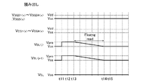
上記のように構成された第1実施形態に係る不揮発性半導体記憶装置10は、読み出し動作を行なう際、図8A〜図8Cに示すように動作する。読み出し動作は、i番目のメモリブロックMB<i>におけるドレイン側選択ゲート線SGD2に接続されたメモリストリングMSを対象とする。さらに、読み出し動作は、それらメモリストリングMSに含まれ、ワード線WL2がゲートに接続されたメモリトランジスタMTr2を対象とする。なお、上記電圧VSGD1<i>〜VSGD4<i>、VSGS<i>、VCG1<i>〜VCG4<i>は、選択された選択ブロックMB<i>を対象とした電圧であり、電圧VSGD1<x>〜VSGD4<x>、VSGS<x>、VCG1<x>〜VCG4<x>は、非選択の非選択ブロックMB<x>(x≠i)を対象とした電圧である。
The nonvolatile
また、第1実施形態に係る不揮発性半導体記憶装置10は、プログラム動作(書き込み動作)を行なう際、図9A〜図9Cに示すように動作する。プログラム動作は、上記読み出し動作と同様のメモリトランジスタMTr2を対象とする。さらに、プログラム動作は、ビット線BL<j>に接続されたメモリトランジスタMTr2に「0」書き込みを行い、ビット線BL<j+1>に接続されたメモリトランジスタMTr2に「1」書き込みを行うものとする。
The nonvolatile
また、第1実施形態に係る不揮発性半導体記憶装置10は、消去動作を行なう際、図10A〜図10Cに示すように動作する。消去動作は、i番目のメモリブロックMB<i>全体を対象とする。
Also, the nonvolatile
(第1実施形態に係る不揮発性半導体記憶装置10の積層構造)
次に、上記図4にて概略を説明した第1実施形態に係る不揮発性半導体記憶装置10の積層構造について、図11〜図16を用いてさらに詳細に説明する。図11は、第1実施形態に係る不揮発性半導体記憶装置10のロウ方向断面図を示す。図12は、第1実施形態に係る不揮発性半導体記憶装置10のカラム方向断面図を示す。図13は、第1実施形態に係る不揮発性半導体記憶装置10の上面図を示す。図14及び図15は、図11の一部拡大図である。図11〜図13においては、層間絶縁層を省略して記載している。
(Laminated structure of the nonvolatile
Next, the stacked structure of the nonvolatile
メモリトランジスタ領域AR1は、図11に示すように、半導体基板Baに設けられたn+拡散層Ba1を有する。また、メモリトブロックMB(メモリトランジスタ領域AR1)は、半導体基板Ba上に順次、ソース側選択トランジスタ層20、メモリトランジスタ層30、及びドレイン側選択トランジスタ層40を有する。ソース側選択トランジスタ層20は、ソース側選択トランジスタSSTrとして機能する。メモリトランジスタ層30は、メモリトランジスタMTr1〜MTr4として機能する。ドレイン側選択トランジスタ層40は、ドレイン側選択トランジスタSSTrとして機能する。
As shown in FIG. 11, the memory transistor region AR1 includes an n + diffusion layer Ba1 provided in the semiconductor substrate Ba. In addition, the memory block MB (memory transistor area AR1) includes a source-side
ソース側選択トランジスタ層20は、図11に示すように、ソース側導電層21、ソース側柱状半導体層22を有する。ソース側導電層21は、図12及び図13に示すように、半導体基板Baと平行な所定領域に亘って延び、メモリブロックMB毎に分断されている。ソース側柱状半導体層22は、ソース側導電層21を貫通して半導体基板Baに達するように柱状に形成されている。ソース側柱状半導体層22は、図13に示すように、上方からみてマトリクス状に形成されている。ソース側柱状半導体層22は、カラム方向に並ぶように形成されている。ソース側柱状半導体層22は、一つのメモリブロックMBに、n行、4列形成されている。ソース側導電層21及びソース側柱状半導体層22は、ポリシリコン(p−Si)にて構成されている。
As shown in FIG. 11, the source side
また、ソース側選択トランジスタ層20は、図14に示すように、ソース側ゲート絶縁層23を有する。ソース側ゲート絶縁層23は、ソース側導電層21とソース側柱状半導体層22との間に形成されている。ソース側ゲート絶縁層23は、酸化シリコン(SiO2)にて構成されている。
Further, the source side
上記ソース側選択トランジスタ層20の構成において、ソース側選択トランジスタSSTrは、ソース側柱状半導体層22を中心に構成される。ソース側導電層21は、ソース側選択トランジスタSSTrの制御ゲートとして機能する。また、ソース側導電層21は、ソース側選択ゲート線SGSの一部として機能する。
In the configuration of the source side
また、ソース側選択トランジスタ層20に係る構成を換言すると、ソース側導電層21は、ロウ方向にn行配列され、カラム方向に4列配列された32個のソース側柱状半導体層22を取り囲むように形成されている。ソース側柱状半導体層22は、後述するメモリ柱状半導体層32から下方に延びるように形成されている。すなわち、ソース側導電層21を32本のソース側柱状半導体層22が貫通する。
In other words, in other words, the source-side
メモリトランスジスタ層30は、図11に示すように、4層に積層されたワード線導電層31(31a〜31d)、メモリ柱状半導体層32を有する。ワード線導電層31a〜31dは、図12及び図13に示すように、半導体基板Baと平行な所定領域に亘って延び、メモリブロックMB毎に分断されている。ワード線導電層31a〜31dは、図11では図示しない層間絶縁層を挟んで積層されている。ワード線導電層31a〜31dは、ロウ方向の両端で階段状に形成されている。メモリ柱状半導体層32は、積層方向に延び且つワード線導電層31a〜31dを貫通するように形成されている。メモリ柱状半導体層32は、図13に示すように、上方からみてマトリクス状に形成されている。メモリ柱状半導体層32は、カラム方向に並ぶように形成されている。メモリ柱状半導体層32は、一つのメモリブロックMBに、n行、4列形成されている。ワード線導電層31a〜31d、及びメモリ柱状半導体層32は、ポリシリコン(p−Si)にて構成されている。
As shown in FIG. 11, the
また、メモリトランジスタ層40は、図15に示すように、トンネル絶縁層33、電荷蓄積層34、及びブロック絶縁層35を有する。トンネル絶縁層33、電荷蓄積層34、及びブロック絶縁層35は、ワード線導電層31とメモリ柱状半導体層32との間に形成されている。メモリ柱状半導体層32側からワード線導電層31側へと順に、トンネル絶縁層33、電荷蓄積層34、及びブロック絶縁層35が形成されている。トンネル絶縁層33及びブロック絶縁層35は、酸化シリコン(SiO2)にて構成されている。電荷蓄積層34は、窒化シリコン(SiN)にて構成されている。
Further, the
上記メモリトランジスタ層30の構成において、メモリストリングMS(メモリトランジスタMTr1〜MTr4)は、メモリ柱状半導体層32を中心に構成される。ワード線導電層31a〜31dは、メモリトランジスタMTr1〜MTr4の制御ゲートとして機能する。また、ワード線導電層31a〜31dは、ワード線WL1〜WL4として機能する。
In the configuration of the
また、メモリトランジスタ層30に係る構成を換言すると、ワード線導電層31a〜31dは、1つのメモリブロックMBにおいて、「ロウ方向にn行配列され、カラム方向に4列配列されたメモリ柱状半導体層32」を取り囲むように(n×4=4n個のメモリ柱状半導体層32を共通接続するように)形成されている。すなわち、ワード線導電層31a〜31dを32本のメモリ柱状半導体層32が貫通する。
In other words, in other words, the word line
ドレイン側選択トランジスタ層40は、図11に示すように、ドレイン側導電層41a、ドレイン側柱状半導体層42を有する。ドレイン側導電層41は、図12及び図13に示すように、ロウ方向に延び、カラム方向に並ぶように形成されている。また、ドレイン側導電層41は、メモリブロックMB毎に、分断されている。ドレイン側導電層41は、1つのメモリブロックMBあたり、4列並んで設けられている。各々のドレイン側柱状半導体層42は、ドレイン側導電層41を貫通するように柱状に形成されている。ドレイン側柱状半導体層42は、図13に示すように、上方からみてマトリクス状に形成されている。ドレイン側柱状半導体層42は、カラム方向に並ぶように形成されている。ドレイン側柱状半導体層42は、一つのメモリブロックMBあたり、n行、4列形成されている。ドレイン側導電層41及びドレイン側柱状半導体層42は、ポリシリコン(p−Si)にて構成されている。
As illustrated in FIG. 11, the drain side
また、ドレイン側選択トランジスタ層40は、図14に示すように、ドレイン側ゲート絶縁層43を有する。ドレイン側ゲート絶縁層43は、ドレイン側導電層41とドレイン側柱状半導体層42との間に形成されている。ドレイン側ゲート絶縁層43は、酸化シリコン(SiO2)にて構成されている。
The drain side
上記ドレイン側選択トランジスタ層40の構成において、ドレイン側選択トランジスタSDTrは、ドレイン側柱状半導体層42を中心に構成される。各ドレイン側導電層41は、ドレイン側トランジスタSDTrの制御ゲートとして機能する。また、ドレイン側導電層41は、ドレイン側選択ゲート線SGDの一部として機能する。
In the configuration of the drain side
また、ドレイン側選択トランジスタ層40に係る構成を換言すると、4つのドレイン側導電層41は、1つのメモリブロックMBにおいて、「ロウ方向にn行配列され、カラム方向に4列配列されたドレイン側柱状半導体層42」を取り囲むように(各々n×1=n個のドレイン側柱状半導体層42を共通接続するように)形成されている。ドレイン側柱状半導体層42は、メモリ柱状半導体層32から上方に延びるように形成されている。すなわち、各ドレイン側導電層41をn本のドレイン側柱状半導体層42が貫通する。
In other words, the configuration relating to the drain-side
また、上記メモリトランジスタ領域AR1に係る構成において、メモリストリングMSは、図13に示すように、メモリブロックMBあたり、カラム方向に4列配列されている。 In the configuration related to the memory transistor area AR1, the memory strings MS are arranged in four columns in the column direction per memory block MB as shown in FIG.
また、第1実施形態に係る不揮発性半導体記憶装置10は、図11に示すように、メモリトランジスタ領域AR1、及び周辺領域AR2に延びる配線層50、及びビット線層60を備える。配線層50、及びビット線層60は、ドレイン側選択トランジスタ層40の上層に形成されている。配線層50、及びビット線層60は、同層に形成されている。なお、ビット線層60は、ビット線BLとして機能する。
In addition, as shown in FIG. 11, the nonvolatile
配線層50は、ワード接続層51、ソース側接続層52、及びドレイン側接続層53を備える。
The
ワード接続層51は、図13に示すように、ロウ方向に延びる矩形状に形成されている。ワード接続層51は、1つのメモリブロックMBあたり、カラム方向に「4列」並んで設けられている。ワード接続層51は、図11、図13に示すように、ワード線導電層31a〜31dのロウ方向一端側において、各々ワード線導電層31a〜31dにコンタクトプラグ層511を介して電気的に接続されている。
As shown in FIG. 13, the
ソース側接続層52は、図13に示すように、ロウ方向に延びる矩形状に形成されている。ソース側接続層52は、1つのメモリブロックMBあたり、「1列」設けられている。ソース側接続層52は、図11、図13に示すように、ワード線導電層31a〜31dのロウ方向他端側(ワード接続層51が接続されるワード線導電層31a〜31dとは反対側)において、ソース側導電層21にコンタクトプラグ層521を介して電気的に接続されている。
As shown in FIG. 13, the source
ドレイン側接続層53は、図13に示すように、ロウ方向に延びる矩形状に形成されている。ドレイン側接続層53は、1つのメモリブロックMBあたり、カラム方向に「4列」並んで設けられている。ドレイン側接続層53は、図11、図13に示すように、ワード線導電層31a〜31dのロウ方向他端側において、ドレイン側導電層42にコンタクトプラグ層531を介して電気的に接続されている。
As shown in FIG. 13, the drain
ビット線層60は、図13に示すように、カラム方向に延びる矩形状に形成されている。ビット線層60は、1つのメモリブロックMBあたりロウ方向にn行並んで形成されている。各々のビット線層60は、各々のドレイン側柱状半導体層42の上端に接続されている。
As shown in FIG. 13, the
すなわち、第1実施形態に係る不揮発性半導体記憶装置10は、以下の(構成1)、(構成2)をもって構成されている。
That is, the nonvolatile
(構成1)ワード接続層51について
・ワード線導電層31のロウ方向の一端近傍へと片側から延びている
(構成2)メモリトストリングスMSについて
・1つのメモリブロックMB毎のカラム方向の
メモリストリングMSの配列数「m」 ・・・ 4
・ワード線導電層31の積層数「n」 ・・・ 4
(構成1)、(構成2)を踏まえると、第1実施形態に係る不揮発性半導体記憶装置10は、以下の(数式1)の関係を満たすように構成されている。
(Configuration 1) Word connection layer 51-Word line
Number of stacked word line
Based on (Configuration 1) and (Configuration 2), the nonvolatile
![]()
![]()
(第1実施形態に係る不揮発性半導体記憶装置10の効果)
次に、第1実施形態に係る不揮発性半導体記憶装置10の効果について説明する。上記に示したように、第1実施形態に係る不揮発性半導体記憶装置10は、(数式1)に示す関係を満たすように構成されている。したがって、第1実施形態に係る不揮発性半導体記憶装置10は、ワード接続層51の占有面積の増大を抑制し、不揮発性半導体記憶装置10全体の占有面積を縮小することができる。
(Effect of Nonvolatile
Next, effects of the nonvolatile
なお、カラム方向のメモリストリングMSをさらに複数列囲むようにワード線導電層31a〜31dを形成したとしても、第1転送トランジスタ172a〜175aの駆動力をメモリストリグスMSの数に比例させて高める必要はない。なぜなら、ワード線導電層31a〜31dのCR時定数は、非常に大きい。そのため、例えば、カラム方向に第1実施形態の2倍の数のメモリストリングMSを囲むようにワード線導電層31a〜31dを形成した場合、ワード線駆動回路110の駆動力を2倍にしても、その立ち上がりや立ち下がりの速度は、ほとんど改善しない。つまり、第1転送トランジスタ172a〜175aの数が減れば、その分だけ単純に、ワード線駆動回路110の面積が減る。
Even if the word line
[第2実施形態]
(第2実施形態に係る不揮発性半導体記憶装置10Aの積層構造)
次に、図16〜図18を参照して、第2実施形態に係る不揮発性半導体記憶装置10Aの積層構造について説明する。図16は、第2実施形態に係る不揮発性半導体記憶装置10Aのロウ方向断面図である。また、図17は、そのカラム方向断面図であり、図18は、その上面図である。図16〜図18は、層間絶縁層を省略して記載している。なお、第2実施形態において、第1実施形態と同様の構成については、同一符号を付し、その説明を省略する。
[Second Embodiment]
(Laminated structure of the nonvolatile
Next, a stacked structure of the nonvolatile
図16〜図18に示すように、第2実施形態に係る不揮発性半導体記憶装置10Aは、第1実施形態と異なるソース側選択トランジスタ層20a、メモリトランジスタ層30a、ドレイン側選択トランジスタ層40a、及び配線層50aを有する。
As shown in FIGS. 16 to 18, the nonvolatile
ソース側選択トランジスタ層20aは、第1実施形態と異なるソース側導電層21aを有する。ソース側導電層21aは、ロウ方向にn行配列され且つカラム方向に6列配列されたソース側柱状半導体層22を取り囲むように(n×6=6n個のソース側柱状半導体層22を共通接続するように)形成されている。
The source side
メモリトランジスタ層30aは、第1実施形態のワード線導電層31a〜31dと異なるワード線導電層31A(31Aa〜31Ad)を有する。ワード線導電層31Aa〜31Adは、ロウ方向にn行配列され且つカラム方向に6列配列されたメモリ柱状半導体層32を取り囲むように(n×6=6n個のメモリ柱状半導体層32を共通接続するように)形成されている。換言すると、ワード線導電層31Aa〜31Adは、各メモリブロックMB内のカラム方向に並ぶ6つのメモリストリングスMSをまとめている。第2実施形態において、1つのメモリブロックMB毎のカラム方向のメモリストリングスMSの配列数「6」は、それらの積層数である「4」よりも大である。なお、ワード線導電層31Aa〜31Adは、第1実施形態と同様に、ローデコーダ回路に接続され、対応する転送トランジスタにより駆動される(図示略)。
The
ドレイン側選択トランジスタ層40aは、第1実施形態と異なるドレイン側導電層41aを有する。ドレイン側導電層41aは、メモリブロックMBあたり、カラム方向に3列配列されている。ドレイン側導電層41aは、メモリブロックMB毎にロウ方向において分断されている。ドレイン側導電層41aは、「ロウ方向にn行配列され且つカラム方向に1列配列されたドレイン側柱状半導体層42」を取り囲むように形成されている。
The drain side
配線層50aは、第1実施形態と異なるワード接続層51a、ソース側接続層52a及びドレイン側接続層53aを有する。
The
ワード接続層51aは、図18に示すように、ワード線導電層31Aa〜31Adのロウ方向両端において、各々ワード線導電層41aa〜41adにコンタクトプラグ層511を介して電気的に接続されている。ワード接続層51aは、1つのメモリブロックMBあたり、ワード線導電層31Aa〜31Adのロウ方向一端側に「2列」設けられている。また、ワード接続層51aは、1つのメモリブロックMBあたり、ワード線導電層31Aa〜31Adのロウ方向他端側に「2列」設けられている。
As shown in FIG. 18, the
ソース側接続層52aは、図18に示すように、ワード線導電層31Aa〜31Adのロウ方向一端側において、各々ソース側導電層21aにコンタクトプラグ521を介して電気的に接続されている。ソース側接続層52aは、1つのメモリブロックMBあたり、ロウ方向一端側に「1列」設けられている。
As shown in FIG. 18, the source
ドレイン側接続層53aは、図18に示すように、ワード線導電層31Aa〜31Adのロウ方向他端側において、各々ドレイン側導電層41aにコンタクトプラグ531を介して電気的に接続されている。ドレイン側接続層53aは、1つのメモリブロックMBあたり、ロウ方向一端側に「3列」設けられている。また、ドレイン側接続層53aは、1つのメモリブロックMBあたり、ロウ方向他端側に「3列」設けられている。
As shown in FIG. 18, the drain
すなわち、第2実施形態に係る不揮発性半導体記憶装置10Aは、第1実施形態と異なる(構成1a)及び(構成2a)をもって形成されている。
That is, the nonvolatile
(構成1a)ワード接続層51aについて
・ワード線導電層31Aのロウ方向の両端近傍へと両側から延びている
(構成2a)メモリストリングMSについて
・1つのメモリブロックMB毎のカラム方向の
メモリストリングMSの配列数「m」 ・・・ 3
・ワード線導電層31Aの積層数「n」 ・・・ 4
(構成1a)、(構成2a)を踏まえると、第2実施形態に係る不揮発性半導体記憶装置10Aは、以下の(数式2)の関係を満たすように構成されている。
(Configuration 1a) Regarding the
Number of stacked word line conductive layers 31A “n” 4
Based on (Configuration 1a) and (Configuration 2a), the nonvolatile
(第2実施形態に係る不揮発性半導体記憶装置10Aの効果)
次に、第2実施形態に係る不揮発性半導体記憶装置10Aの効果について説明する。第2実施形態に係る不揮発性半導体記憶装置10Aは、上記(数式2)の関係を満たすように構成されているので、第1実施形態と同様の効果を奏する。
(Effects of Nonvolatile
Next, effects of the nonvolatile
[第3実施形態]
(第3実施形態に係る不揮発性半導体記憶装置10Cの概略構成)
次に、図19を参照して、第3実施形態に係る不揮発性半導体記憶装置10Bの概略構成について説明する。図19は、第3実施形態に係る不揮発性半導体記憶装置10Bの回路図である。なお、第3実施形態において、第1及び第2実施形態と同様の構成については、同一符号を付し、その説明を省略する。
[Third Embodiment]
(Schematic configuration of the nonvolatile
Next, a schematic configuration of the nonvolatile
図19に示すように、第3実施形態に係る不揮発性半導体記憶装置10Bは、メモリトランジスタ領域ARa1、及びその周辺に設けられた周辺領域ARa2を有する。メモリトランジスタ領域ARa1は、電気的に書き換え可能なメモリトランジスタMTra1〜MTra8(メモリセル)を有する領域である。周辺領域ARa2は、メモリトランジスタMTra1〜MTra8等へ与える電圧を制御する各種制御回路を有する領域である。
As illustrated in FIG. 19, the nonvolatile
メモリトランジスタ領域ARa1は、n行、2列のメモリストリングMSaを有する複数のメモリブロックMBaを備える。メモリストリングMSaは、基板と平行な方向からみて「U字状」に形成されている。メモリストリングMSaは、図20に示すように、8つの電気的に書き換え可能なメモリトランジスタMTra1〜MTra8が直列接続された構成を有する。メモリストリングMSaの一端、及び他端には、ソース側選択トランジスタSSTra、及びドレイン側選択トランジスタSDTraが設けられている。ソース側選択トランジスタSSTra、及びドレイン側選択トランジスタSDTraは、メモリストリングMSaの導通を制御する。メモリトランジスタMTra1〜MTra8の制御ゲートは、ワード線WLa1〜WLa8に接続されている。ソース側選択トランジスタSSTraの制御ゲートは、ソース側選択ゲート線SGSaに接続されている。ドレイン側選択トランジスタSDTraの制御ゲートは、ドレイン側選択ゲート線SGDaに接続されている。 The memory transistor area ARa1 includes a plurality of memory blocks MBa having n rows and two columns of memory strings MSa. The memory string MSa is formed in a “U shape” when viewed from a direction parallel to the substrate. As shown in FIG. 20, the memory string MSa has a configuration in which eight electrically rewritable memory transistors MTra1 to MTra8 are connected in series. At one end and the other end of the memory string MSa, a source side selection transistor SSTRA and a drain side selection transistor SDTr are provided. The source side select transistor SSTRA and the drain side select transistor SDTr control the conduction of the memory string MSa. Control gates of the memory transistors MTra1 to MTra8 are connected to the word lines WLa1 to WLa8. The control gate of the source side select transistor SSTRA is connected to the source side select gate line SGSa. The control gate of the drain side select transistor SDTr is connected to the drain side select gate line SGDa.
また、第3実施形態において、ワード線WLa1〜WLa8は、1つのメモリブロックMBaにおいてカラム方向に隣接する2つのメモリストリングMSaにて共有されている。換言すると、ワード線WLa1〜WLa8は、1つのメモリブロックMBaにおいてカラム方向に隣接する2つのメモリストリングMSaをまとめている。また、詳細は後述するが、ワード線WLa1とワード線WLa8は、同層に形成されている。ワード線WLa2とワード線WLa7は、同層に形成されている。ワード線WLa3とワード線WLa6は、同層に形成されている。ワード線WLa4とワード線WLa5は、同層に形成されている。すなわち、ワード線WLa1〜WLa8は、4層にて構成されている。なお、ワード線WLa1〜WLa8は、各メモリブロックMBaに対応するローデコーダ回路へ接続されている(図示略)。 In the third embodiment, the word lines WLa1 to WLa8 are shared by two memory strings MSa adjacent in the column direction in one memory block MBa. In other words, the word lines WLa1 to WLa8 group two memory strings MSa adjacent in the column direction in one memory block MBa. Although details will be described later, the word line WLa1 and the word line WLa8 are formed in the same layer. The word line WLa2 and the word line WLa7 are formed in the same layer. The word line WLa3 and the word line WLa6 are formed in the same layer. The word line WLa4 and the word line WLa5 are formed in the same layer. That is, the word lines WLa1 to WLa8 are composed of four layers. The word lines WLa1 to WLa8 are connected to a row decoder circuit corresponding to each memory block MBa (not shown).
ここで、図21を参照して、メモリトランジスタ領域ARa1の積層構造の概略を説明する。図22は、メモリトランジスタ領域ARa1の積層構造を示す概略図である。 Here, an outline of the stacked structure of the memory transistor region ARa1 will be described with reference to FIG. FIG. 22 is a schematic diagram showing a stacked structure of the memory transistor region ARa1.
メモリトランジスタ領域ARa1は、第1実施形態と異なる半導体基板Baa上に形成されている。基板Baaは、第1実施形態のようにn+拡散層Ba1を有していない。 The memory transistor area ARa1 is formed on a semiconductor substrate Baa different from the first embodiment. The substrate Baa does not have the n + diffusion layer Ba1 as in the first embodiment.
メモリスブロックMBa(メモリトランジスタ領域ARa1)は、メモリストリングMSa毎に設けられたU字状半導体SC、ワード線WLa1〜WLa8、バックゲート線BGaを有する。 The memory block MBa (memory transistor area ARa1) includes a U-shaped semiconductor SC, word lines WLa1 to WLa8, and a back gate line BGa provided for each memory string MSa.
U字状半導体SCは、ロウ方向からみてU字状に形成されている。すなわち、U字状半導体SCは、半導体基板Baaに対して略垂直方向に延びる一対の柱状部CLa、及び一対の柱状部CLaの下端を連結させるように形成された連結部JPaを有する。なお、柱状部CLaは、円柱状であっても、角柱状であってもよい。また、柱状部CLaは、段々形状を有する柱状であってもよい。ここで、ロウ方向は、積層方向に直交する方向であり、後述するカラム方向は、積層方向及びロウ方向に直交する方向である。 The U-shaped semiconductor SC is formed in a U shape when viewed from the row direction. That is, the U-shaped semiconductor SC includes a pair of columnar portions CLa extending in a substantially vertical direction with respect to the semiconductor substrate Baa and a connection portion JPa formed so as to connect the lower ends of the pair of columnar portions CLa. Note that the columnar portion CLa may be a columnar shape or a prismatic shape. Further, the columnar part CLa may be a columnar shape having a stepped shape. Here, the row direction is a direction orthogonal to the stacking direction, and a column direction to be described later is a direction orthogonal to the stacking direction and the row direction.
U字状半導体SCは、一対の柱状部CLaの中心軸を結ぶ直線がカラム方向に平行になるように配置されている。また、U字状半導体SCは、ロウ方向及びカラム方向から構成される面内にマトリクス状となるように配置されている。 The U-shaped semiconductor SC is arranged so that a straight line connecting the central axes of the pair of columnar portions CLa is parallel to the column direction. Further, the U-shaped semiconductor SC is arranged in a matrix form in a plane constituted by the row direction and the column direction.
各層のワード線WLa1〜WLa8は、ロウ方向に平行に延びる形状を有している。各層のワード線WLa1〜WLa8は、カラム方向に並び、互いに絶縁分離して形成されている。ワード線WLa1は、ワード線WLa8と同層に形成されている。同様に、ワード線WLa2は、ワード線WLa7と同層に形成され、ワード線WLa3は、ワード線WLa6と同層に形成され、ワード線WLa4は、ワード線WLa5と同層に形成されている。 The word lines WLa1 to WLa8 of each layer have a shape extending in parallel to the row direction. The word lines WLa1 to WLa8 of each layer are formed in the column direction so as to be insulated from each other. The word line WLa1 is formed in the same layer as the word line WLa8. Similarly, the word line WLa2 is formed in the same layer as the word line WLa7, the word line WLa3 is formed in the same layer as the word line WLa6, and the word line WLa4 is formed in the same layer as the word line WLa5.
カラム方向の同位置に設けられロウ方向に並ぶメモリトランジスタMTra1〜MTra8のゲートは、同一のワード線WLa1〜WLa8に接続されている。各ワード線WLa1〜WLa8のロウ方向の端部は、階段状に形成されている。各ワード線WLa1〜WLa8は、ロウ方向に複数並ぶ柱状部CLaを取り囲むように形成されている。 The gates of the memory transistors MTra1 to MTra8 provided at the same position in the column direction and arranged in the row direction are connected to the same word lines WLa1 to WLa8. The end portions in the row direction of the word lines WLa1 to WLa8 are formed in a staircase shape. Each of the word lines WLa1 to WLa8 is formed so as to surround a plurality of columnar portions CLa arranged in the row direction.
図22に示すように、ワード線WLa1〜WLa8と柱状部CLaとの間には、ONO(Oxide-Nitride-Oxide)層NLが形成されている。ONO層NLは、柱状部CLaに接するトンネル絶縁層TI、トンネル絶縁層TIに接する電荷蓄積層EC、及び電荷蓄積層ECに接するブロック絶縁層BIを有する。電荷蓄積層ECは、電荷を蓄積する機能を有する。上記構成を換言すると、電荷蓄積層ECは、柱状部CLaの側面を取り囲むように形成されている。各ワード線WLa1〜WLa8は、電荷蓄積層ECを取り囲むように形成されている。 As shown in FIG. 22, an ONO (Oxide-Nitride-Oxide) layer NL is formed between the word lines WLa1 to WLa8 and the columnar part CLa. The ONO layer NL includes a tunnel insulating layer TI in contact with the columnar portion CLa, a charge storage layer EC in contact with the tunnel insulating layer TI, and a block insulating layer BI in contact with the charge storage layer EC. The charge storage layer EC has a function of storing charges. In other words, the charge storage layer EC is formed so as to surround the side surface of the columnar portion CLa. Each of the word lines WLa1 to WLa8 is formed so as to surround the charge storage layer EC.
ドレイン側選択トランジスタSDTraは、柱状半導体SCa、ドレイン側選択ゲート線SGDaを有する。柱状半導体SCaは、一方の柱状部CLaの上面から上方に基板Baに対して垂直方向に延びるように形成されている。ドレイン側選択ゲート線SGDaは、最上部のワード線WLa1の上部に設けられている。ドレイン側選択ゲート線SGDaは、ロウ方向に平行に延びる形状を有している。ドレイン側選択ゲート線SGDaは、カラム方向に並び、後述するソース側選択ゲート線SGSaを挟むように、ライン状に繰り返し形成されている。ドレイン側選択ゲート線SGDaは、ロウ方向に複数並ぶ柱状半導体SCaを取り囲むように形成されている。図22に示すように、ドレイン側選択ゲート線SGDaと柱状半導体SCaとの間には、ゲート絶縁層DGIが形成されている。上記構成を換言すると、各ドレイン側選択ゲート線SGDは、ゲート絶縁層DGIを取り囲むように形成されている。 The drain side select transistor SDTr includes a columnar semiconductor SCa and a drain side select gate line SGDa. The columnar semiconductor SCa is formed to extend upward from the upper surface of one columnar portion CLa in a direction perpendicular to the substrate Ba. The drain side select gate line SGDa is provided above the uppermost word line WLa1. The drain side select gate line SGDa has a shape extending in parallel to the row direction. The drain side select gate lines SGDa are repeatedly formed in a line so as to be arranged in the column direction and sandwich a source side select gate line SGSa described later. The drain side select gate line SGDa is formed so as to surround a plurality of columnar semiconductors SCa arranged in the row direction. As shown in FIG. 22, a gate insulating layer DGI is formed between the drain side select gate line SGDa and the columnar semiconductor SCa. In other words, each drain-side selection gate line SGD is formed so as to surround the gate insulating layer DGI.
ソース側選択トランジスタSSTraは、柱状半導体SCb、ソース側選択ゲート線SGSaを有する。柱状半導体SCbは、他方の柱状部CLaの上面から上方に延びるように形成されている。ソース側選択ゲート線SGSaは、最上部のワード線WLa8の上部に設けられている。ソース側選択ゲート線SGSaは、ロウ方向に平行に延びる形状を有している。ソース側選択ゲート線SGSaは、カラム方向に並び、上述したドレイン側選択ゲート線SGDaを間に挟んで、ライン状に繰り返し形成されている。ソース側選択ゲート線SGSaは、ロウ方向に複数行並ぶ柱状半導体SCbを取り囲むように形成されている。図22に示すように、ソース側選択ゲート線SGSaと柱状半導体SCbとの間には、ゲート絶縁層SGIが形成されている。上記構成を換言すると、各ドレイン側選択ゲート線SGSaは、ゲート絶縁層SGIを取り囲むように形成されている。 The source side select transistor SSTra includes a columnar semiconductor SCb and a source side select gate line SGSa. The columnar semiconductor SCb is formed to extend upward from the upper surface of the other columnar portion CLa. The source side select gate line SGSa is provided above the uppermost word line WLa8. The source side select gate line SGSa has a shape extending in parallel to the row direction. The source side select gate lines SGSa are repeatedly arranged in a line in the column direction with the drain side select gate line SGDa interposed therebetween. The source side select gate line SGSa is formed so as to surround the columnar semiconductors SCb arranged in a plurality of rows in the row direction. As shown in FIG. 22, a gate insulating layer SGI is formed between the source side select gate line SGSa and the columnar semiconductor SCb. In other words, each drain-side selection gate line SGSa is formed so as to surround the gate insulating layer SGI.
バックゲート線BGaは、複数の連結部JPaの下部を覆うように、ロウ方向及びカラム方向に2次元的に所定範囲に亘って延びるように形成されている。図22に示すように、バックゲート線BGaと連結部JPaとの間には、上述したONO層NLが形成されている。 The back gate line BGa is formed so as to extend over a predetermined range two-dimensionally in the row direction and the column direction so as to cover the lower portions of the plurality of connecting portions JPa. As shown in FIG. 22, the above-described ONO layer NL is formed between the back gate line BGa and the connecting portion JPa.
図21に戻って説明を続ける。柱状半導体SCbは、カラム方向に隣接して形成されている。一対の柱状半導体SCbの上端には、ソース線SLaが接続されている。ソース線SLaは、一対の柱状半導体SCbに対して共通に設けられている。 Returning to FIG. 21, the description will be continued. The columnar semiconductor SCb is formed adjacent to the column direction. A source line SLa is connected to the upper ends of the pair of columnar semiconductors SCb. The source line SLa is provided in common to the pair of columnar semiconductors SCb.
ドレイン側選択ゲート線SGDaにて取り囲まれた柱状半導体SCaの上端には、プラグ線PLを介してビット線BLaが形成されている。各ビット線BLaは、ソース線SLaよりも上方に位置するように形成されている。各ビット線BLaは、ロウ方向に所定間隔を設けてカラム方向に延びるライン状に繰り返し形成されている。 A bit line BLa is formed on the upper end of the columnar semiconductor SCa surrounded by the drain side select gate line SGDa via the plug line PL. Each bit line BLa is formed to be positioned above the source line SLa. Each bit line BLa is repeatedly formed in a line extending in the column direction with a predetermined interval in the row direction.
再び、図19を参照して、周辺領域ARa2について説明する。周辺領域ARa2は、ワード線駆動回路110a、110b、選択ゲート線駆動回路120a、120b、アドレスデコーダ回路130、昇圧回路140A〜140C、センスアンプ回路150、ソース線駆動回路160、第1ロウデコーダ回路180a、第2ロウデコーダ回路180b、及びバックゲート線駆動回路190を有する。
Again, the peripheral area ARa2 will be described with reference to FIG. The peripheral area ARa2 includes word
ワード線駆動回路110aは、ワード線WLa1〜WLa4を駆動するための電圧VCG1a〜VCG4aを転送する。ワード線駆動回路110bは、ワード線WLa5〜WLa8を駆動するための電圧VCG1b〜VCG4bを転送する。選択ゲート線駆動回路120aは、ソース側選択ゲート線SGSa1を駆動するための電圧VSGS1を転送する。選択ゲート線駆動回路120bは、ソース側選択ゲート線SGSa2を駆動するための電圧VSGS2を転送する。アドレスデコーダ130は、第1実施形態と同様に、ブロックアドレスを指定するための電圧VBADを出力する。
Word
昇圧回路140Aは、基準電圧から昇圧させた電圧を、ワード線駆動回路110a、110bに転送する。昇圧回路140Bは、基準電圧から昇圧させた電圧VRDECを、第1、第2ロウデコーダ回路180a、180bに転送する。
The
第1、第2ロウデコーダ回路180a、180bは、一つのメモリブロックMBaに対して、各々一つ設けられている。第1ロウデコーダ回路180aは、電圧VBADに基づき、選択的にメモリトランジスタMTra1〜MTra4のゲートに電圧VCG1a<i>〜VCG4a<i>を転送する。また、第1ロウデコーダ回路180aは、電圧VBADに基づき、選択的にソース側選択ゲート線SGSa1に接続されたソース側選択トランジスタSSTraのゲートに電圧VSGS1<i>を転送する。また、第1ロウデコーダ回路180aは、電圧VBADに基づき、選択的に度連側選択ゲート線SGDa2に接続されたドレイン側選択トランジスタSDTraのゲートに電圧VSGD2<i>を転送する。第2ロウデコーダ回路180bは、電圧VBADに基づき、選択的にメモリトランジスタMTra5〜MTra8のゲートに電圧VCG1b<i>〜VCG4b<i>を転送する。また、第2ロウデコーダ回路180bは、電圧VBADに基づき、選択的にソース側選択ゲート線SGSa2に接続されたソース側選択トランジスタSSTraのゲートに電圧VSGS2<i>を転送する。また、第2ロウデコーダ回路180bは、電圧VBADに基づき、選択的にドレイン側選択ゲート線SGDa1に接続されたドレイン側選択トランジスタSDTraのゲートに電圧VSGD1<i>を転送する。
One first and second
第1ロウデコーダ回路180aは、電圧変換回路181a、第1転送トランジスタ182a〜185a、第2転送トランジスタ186a、187a、及び第3転送トランジスタ188a、189aを有する。電圧変換回路181aは、受け付けた電圧VRDECを変換して電圧VSELa<i>を生成し、第1、第2転送トランジスタ182a〜187aのゲートに出力する。第1転送トランジスタ182a〜185aは、ワード線駆動回路110aと各ワード線WLa1〜WLa4との間に接続されている。第1転送トランジスタ182a〜185aは、電圧VCG1a〜VCG4a、VSELa<i>に基づき、ワード線WLa1〜WLa4に電圧VCG1a<1>〜VCG4a<i>を転送する。第2転送トランジスタ186a、187aは、電圧VSGS1、VSGD2、VSGOFF、VSELa<i>に基づき、ソース側選択ゲート線SGSa1、ドレイン側選択ゲート線SGDa2に、電圧VSGS1<i>、VSGD2<i>を転送する。
The first
第2ロウデコーダ回路180bは、電圧変換回路181b、第1転送トランジスタ182b〜185b、第2転送トランジスタ186b、187b、第3転送トランジスタ188b、189b、及び第4転送トランジスタ181cを有する。電圧変換回路181bは、受け付けた電圧VRDECを変換して電圧VSELb<i>を生成し、第1、第2、第4転送トランジスタ182b〜187b、181cのゲートに出力する。第1転送トランジスタ182b〜185bは、ワード線駆動回路110bと各ワード線WLa5〜WLa8との間に接続されている。第1転送トランジスタ182b〜185bは、電圧VCG1b〜VCG4b、VSELb<i>に基づき、ワード線WLa5〜WLa8に電圧VCG1b<1>〜VCG4b<i>を転送する。第2転送トランジスタ186b、187bは、選択ゲート線駆動回路120bと、ソース側選択ゲート線SGS2、ドレイン側選択ゲート線SGD1との間に接続されている。第2転送トランジスタ186b、187bは、電圧VSGS2、VSGD1、VSGOFF、VSELb<i>に基づき、ソース側選択ゲート線SGSa2、ドレイン側選択ゲート線SGDa1に、電圧VSGS2<i>、VSGD1<i>を転送する。第4転送トランジスタ181cは、バックゲート線駆動回路190とバックゲート線BGaとの間に接続されている。第4転送トランジスタ181cは、電圧VBGに基づき、バックゲート線BGに、電圧VBG<i>を転送する。
The second
上記のように構成された第3実施形態に係る不揮発性半導体記憶装置10Bは、読み出し動作を行なう際、図23A〜図23Cに示すように動作する。読み出し動作は、i番目のメモリブロックMBa<i>におけるドレイン側選択ゲート線SGDa2に接続されたメモリストリングMSaを対象とする。さらに、読み出し動作は、それらメモリストリングMSaに含まれ、ワード線WLa2がゲートに接続されたメモリトランジスタMTra2を対象とする。
The nonvolatile
また、第3実施形態に係る不揮発性半導体記憶装置10Bは、プログラム動作(書き込み動作)を行なう際、図24A〜図24Cに示すように動作する。プログラム動作は、上記読み出し動作と同様のメモリトランジスタMTra2を対象とする。さらに、プログラム動作は、ビット線BL<j>に接続されたメモリトランジスタMTra2に「0」書き込みを行い、ビット線BL<j+1>に接続されたメモリトランジスタMTra2に「1」書き込みを行うものとする。
In addition, the nonvolatile
また、第3実施形態に係る不揮発性半導体記憶装置10Bは、消去動作を行なう際、図25A〜図25Cに示すように動作する。消去動作は、i番目のメモリブロックMBa<i>全体を対象とする。
In addition, the nonvolatile
(第3実施形態に係る不揮発性半導体記憶装置10Bの積層構造)
次に、図26〜図28、図29A〜図29Eを参照して、第3実施形態に係る不揮発性半導体記憶装置10Bの積層構造について説明する。図26は、第3実施形態に係る不揮発性半導体記憶装置10Bのロウ方向断面図である。図27は、そのカラム方向断面図である。図28は、その上面図である。図29A〜図29Eは、図28の各層を示す上面図である。なお、図27〜図29、図30A〜図30Eにおいて、層間絶縁層は、省略して記載している。
(Laminated structure of the nonvolatile
Next, with reference to FIGS. 26 to 28 and FIGS. 29A to 29E, a stacked structure of the nonvolatile
第3実施形態に係る不揮発性半導体記憶装置10Bにおいて、メモリブロックMBa(メモリトランジスタ領域ARa1)は、図26〜図28に示すように、半導体基板Baa上に、順次、バックゲートトランジスタ層20b、メモリトランジスタ層30b、及び選択トランジスタ層40bを有する。バックゲートトランジスタ層20bは、バックゲートトランジスタBGTraとして機能する。メモリトランジスタ層30bは、メモリトランジスタMTra1〜MTra8として機能する。選択トランジスタ層40bは、ソース側選択トランジスタSSTra及びドレイン側選択トランジスタ層SDTraとして機能する。
In the nonvolatile
バックゲートトランジスタ層20bは、図26及び図27に示すように、バックゲート導電層21b、底部半導体層22bを有する。バックゲート導電層21bは、半導体基板Baaと平行に所定領域に亘って広がる板状に構成されている。バックゲート導電層21bは、図30Aに示すように、メモリブロックMBa毎に分断されている。底部半導体層22bは、バックゲート導電層21bの上面から所定深さまで形成されている。底部半導体層22bは、図29及び図30Aに示すように、上方から見てカラム方向に延びるように形成されている。底部半導体層22bは、上方からみてマトリクス状に形成されている。底部半導体層22bは、1つのメモリブロックMBaにおいて、ロウ方向に「n行」、カラム方向に「2列」配列されている。バックゲート導電層21A、及び底部半導体層22Aは、ポリシリコン(Si)にて構成されている。
As shown in FIGS. 26 and 27, the back
また、バックゲートトランジスタ層20bは、トンネル絶縁層、電荷蓄積層、及びブロック絶縁層を有する。トンネル絶縁層、電荷蓄積層、及びブロック絶縁層は、バックゲート導電層21Aと底部半導体層22Aとの間に形成されている。トンネル絶縁層、電荷蓄積層、及びブロック絶縁層は、底部半導体層22A側からバックゲート導電層21A側へと順に形成されている。トンネル絶縁層及びブロック絶縁層は、酸化シリコン(SiO2)にて構成されている。電荷蓄積層は、窒化シリコン(SiN)にて構成されている。
The back
上記バックゲートトランジスタ層20bの構成において、バックゲート導電層22bは、バックゲートトランジスタBGTraの制御ゲートとして機能する。また、バックゲート導電層22bは、バックゲート線BGaの一部として機能する。底部半導体層22bは、メモリストリングMSaのU字状の底部を構成する。
In the configuration of the back
メモリトランジスタ層30bは、図26及び図27に示すように、第1ワード線導電層31B(31Ba〜31Bd)、第2ワード線導電層31C(31Ca〜31Cd)、第1メモリ柱状半導体層32b、及び第2メモリ柱状半導体層32cを有する。第1、第2ワード線導電層31Ba〜31Bd、31Ca〜31Cdは、1つのメモリブロックMBa毎に、図28及び図29Bに示すように、カラム方向に並びロウ方向に延びる2つの突出部を有して櫛歯状に形成されている。第1ワード線導電層31Ba〜31Bdの突出部は、所定間隔を設けて第2ワード線導電層31Ca〜31Cdの突出部の間に位置するように形成されている。つまり、第1、第2ワード線導電層31Ba〜31Bd、31Ca〜31Cdの突出部は、1つのメモリブロックMBaあたり、カラム方向に「4」列並ぶ。第1、第2メモリ柱状半導体層32b、32bは、積層方向に延び且つ第1、第2ワード線導電層31Ba〜31Bd、31Ca〜31Cdを貫通するように柱状に形成されている。第1、第2メモリ柱状半導体層32b、32cは、図28及び図29Bに示すように、第1、第2ワード線導電層31Ba〜31Bd、31Ca〜31Cdの突出部にてカラム方向に並ぶように形成されている(上方からみてマトリクス状に形成)。カラム方向に並ぶ一対の第1、第2メモリ柱状半導体層32b、32cは、底部半導体層22Aのカラム方向の両端に各々接続するように形成されている。換言すると、底部半導体層22Aは、第1、第2メモリ柱状半導体層32b、32cの底部を接続するように形成されている。第1、第2ワード線導電層31Ba〜31Bd、31Ca〜31Cd、第1、第2メモリ柱状半導体層32b、32cは、ポリシリコン(p−Si)にて構成されている。
As shown in FIGS. 26 and 27, the
また、メモリトランジスタ層30bは、トンネル絶縁層、電荷蓄積層、及びブロック絶縁層を有する。トンネル絶縁層、電荷蓄積層、及びブロック絶縁層は、第1ワード線導電層31Ba〜31Bdと第1メモリ柱状半導体層32bとの間、及び第2ワード線導電層31Ca〜31Cdと第2メモリ柱状半導体層32cとの間に形成されている。トンネル絶縁層、電荷蓄積層、及びブロック絶縁層は、第1メモリ柱状半導体層32b(第2メモリ柱状半導体層32c)側から第1ワード線導電層31Ba〜31Bd(第2ワード線導電層31Ca〜31Cd)側へと順に形成されている。トンネル絶縁層及びブロック絶縁層は、酸化シリコン(SiO2)にて構成されている。電荷蓄積層は、窒化シリコン(SiN)にて構成されている。
The
上記メモリトランジスタ層30bの構成において、第1、第2ワード線導電層31Ba〜31Bd、31Ca〜31Cdは、メモリトランジスタMTra1〜MTra8の制御ゲートとして機能する。また、第1、第2ワード線導電層31Ba〜31Bd、31Ca〜31Cdは、ワード線WLa1〜WLa8の一部として機能する。第1、第2メモリ柱状半導体層32b、32cは、メモリストリングMSaのU字状の一対の側部を構成する。
In the configuration of the
また、メモリトランジスタ層30bに係る構成を換言すると、第1ワード線導電層31Ba〜31Bdは、「ロウ方向にn行配列され、カラム方向に2列配列された第1メモリ側柱状半導体層32b」を取り囲むように形成されている。第2ワード線導電層31Ca〜31Cdは、「ロウ方向にn行配列され、カラム方向に2列配列された第2メモリ側柱状半導体層32c」を取り囲むように形成されている。 In other words, in other words, the first word line conductive layers 31Ba to 31Bd are “first memory side columnar semiconductor layers 32b arranged in n rows in the row direction and in two columns in the column direction”. It is formed so as to surround. The second word line conductive layers 31Ca to 31Cd are formed so as to surround the “second memory side columnar semiconductor layers 32c arranged in n rows in the row direction and in two columns in the column direction”.
選択トランジスタ層40bは、図26及び図27に示すように、ソース側導電層41b、ドレイン側導電層42b、ソース側柱状半導体層43b、及びドレイン側柱状半導体層44bを有する。ソース側導電層41bは、図28及び図29Cに示すように、カラム方向に並びロウ方向に延びるストライプ状に形成されている。ソース側導電層41bは、1つのメモリブロックMBaあたり、2つ設けられている。ソース側導電層41bは、メモリブロックMBa毎に分断されている。ドレイン側導電層42bは、図30Cに示すように、カラム方向に所定の周期でロウ方向に延びるストライプ状に形成されている。ドレイン側導電層42bは、ソース側導電層41bの間に設けられている。ドレイン側導電層42bは、1つのメモリブロックMBaあたり、2つ設けられている。ドレイン側導電層42bは、メモリブロックMBa毎に分断されている。ソース側柱状半導体層43bは、ソース側導電層41bを貫通して、第1メモリ柱状半導体層32bの上面に接するように形成されている。ソース側柱状半導体層43bは、1つのメモリブロックMBaに対して、n行、2列形成されている。ドレイン側柱状半導体層44bは、ドレイン側導電層42bを貫通して、第2メモリ柱状半導体層32cの上面に接するように形成されている。ドレイン側柱状半導体層44bは、1つのメモリブロックMBaに対して、n行、2列形成されている。
As shown in FIGS. 26 and 27, the
また、選択トランジスタ層40bは、ソース側ゲート絶縁層、及びドレイン側ゲート絶縁層を有する。ソース側ゲート絶縁層は、ソース側導電層41bとソース側柱状半導体層43bとの間に形成されている。ドレイン側ゲート絶縁層は、ドレイン側導電層42bとドレイン側柱状半導体層44bとの間に形成されている。ソース側ゲート絶縁層及びドレイン側ゲート絶縁層は、酸化シリコン(SiO2)にて構成されている。
The
上記選択トランジスタ層40bの構成において、ソース側導電層41bは、ソース側選択トランジスタSSTraの制御ゲートとして機能する。また、ソース側導電層41bは、ソース側選択ゲート線SGSaの一部として機能する。ドレイン側導電層42bは、ドレイン側選択トランジスタSDTraの制御ゲートとして機能する。また、ドレイン側導電層42bは、ドレイン側選択ゲート線SGDaの一部として機能する。
In the configuration of the
また、選択トランジスタ層40bに係る構成を換言すると、ソース側導電層41bは、「ロウ方向にn行配列され、カラム方向に1列配列されたソース側柱状半導体層43b」を取り囲むように形成されている。ドレイン側導電層42bは、「ロウ方向にn行配列され、カラム方向に1列配列されたドレイン側柱状半導体層44b」を取り囲むように形成されている。ソース側柱状半導体層43b及びドレイン側柱状半導体層44bは、第1、第2メモリ柱状半導体層32b、32cから上方に延びるように形成されている。
In other words, in other words, the source-side
上記メモリトランジスタ領域ARa1に係る構成において、メモリストリングMSaは、メモリブロックMBaあたり、図28に示すように、カラム方向に2列配列されている。 In the configuration related to the memory transistor region ARa1, the memory strings MSa are arranged in two columns in the column direction as shown in FIG. 28 per memory block MBa.
また、第3実施形態に係る不揮発性半導体記憶装置10Bは、メモリトランジスタ領域AR1a、及び周辺領域ARa2に延びる配線層50b、ビット線層60b、及びソース線層70を備える。配線層50bとソース線層70は、同層に形成され、ビット線層60bは、それらの上層に形成されている。なお、ソース線層70は、ソース線SLaとして機能する。
In addition, the nonvolatile
配線層50bは、ワード接続層51b、ソース側接続層52b、ドレイン側接続層53b、及びバックゲート接続層54bを備える。
The
ワード接続層51bは、図28、及び図29Dに示すように、ロウ方向に延びる矩形状に形成されている。ワード接続層51bは、1つのメモリブロックMBaあたり、カラム方向に「4列」並んで設けられている。ワード接続層51bは、第1ワード線導電層31Ba〜31Bdのロウ方向一端側において、各々コンタクトプラグ層511bを介して第1ワード線導電層31Ba〜31Bdに電気的に接続されている。また、ワード接続層51bは、第2ワード線導電層31Ca〜31Cdのロウ方向他端側において、各々コンタクトプラグ層511bを介して第2ワード線導電層31Ca〜31Cdに電気的に接続されている。
As shown in FIGS. 28 and 29D, the
ソース側接続層52bは、図28及び図29Dに示すように、ロウ方向に延びる矩形状に形成されている。ソース側接続層52bは、1つのメモリブロックMBaあたり、2つ設けられている。2つのソース側接続層52bのうちの1つは、第1ワード線導電層31Ba〜31Bdのロウ方向一端側において、コンタクトプラグ層521bを介してソース側導電層41bに電気的に接続されている。また、2つのソース側接続層52bのうちの1つは、第2ワード線導電層31Ca〜31Cdのロウ方向他端側において、コンタクトプラグ層521bを介してソース側導電層41bに電気的に接続されている。
As shown in FIGS. 28 and 29D, the source-
ドレイン側接続層53bは、図28及び図29Dに示すように、ロウ方向に延びる矩形状に形成されている。ドレイン側接続層53bは、1つのメモリブロックMBaあたり、2つ設けられている。2つのドレイン側接続層53bのうちの1つは、第1ワード線導電層31Ba〜31Bdのロウ方向一端側において、コンタクトプラグ層531bを介してドレイン側導電層42bに電気的に接続されている。また、2つのドレイン側接続層53bのうちの1つは、第2ワード線導電層31Ca〜31Cdのロウ方向他端側において、コンタクトプラグ層531bを介してドレイン側導電層42bに電気的に接続されている。
As shown in FIGS. 28 and 29D, the drain
バックゲート接続層54bは、図28及び図29Dに示すように、ロウ方向に延びる矩形状に形成されている。バックゲート接続層54bは、1つのメモリブロックMBaあたり、1つ設けられている。バックゲート接続層54bは、第1、第2ワード線導電層31Ba〜31Bd、31Ca〜31Cdのロウ方向一端側(他端側)において、コンタクトプラグ層541bを介してバックゲート導電層21bに電気的に接続されている。
As shown in FIGS. 28 and 29D, the back
ビット線層60bは、図28及び図29Eに示すように、カラム方向に延びる矩形状に形成されている。ビット線層60bは、1つのメモリブロックMBaあたり、ロウ方向にn行並んで形成されている。各々のビット線層60bは、ドレイン側柱状半導体層44bの上面にコンタクトプラグ層61を介して接続されている。なお、ビット線層60bは、ビット線BLaとして機能する。
As shown in FIGS. 28 and 29E, the
ソース線層70は、図28及び図29Dに示すように、カラム方向に延びる梯子状に形成されている。ソース線層70のロウ方向に延びる部分は、1つのメモリブロックMBaにおいて、2つ形成されている。ソース線層70は、それらロウ方向に延びる部分にてソース側柱状半導体層43bの上面に接続されている。
As shown in FIGS. 28 and 29D, the
すなわち、第3実施形態に係る不揮発性半導体記憶装置10Bは、以下の(構成1c)、(構成2c)をもって構成されている。
That is, the nonvolatile
(構成1b)ワード接続層51bについて
・第1、第2ワード線導電層31B、31Cのロウ方向の両端近傍へと両側から延びている
(構成2b)メモリストリングMSaについて
・1つのメモリブロックMBa毎のカラム方向の
メモリストリングMSaの配列数「m」 ・・・ 2
・第1、第2ワード線導電層31B、31Cの積層数「n」 ・・・ 4
(構成1b)、(構成2b)を踏まえると、第3実施形態に係る不揮発性半導体記憶装置10Bは、上記(数式1)の関係を満たすように構成されている。
(Configuration 1b) Regarding the
Number of stacked first and second word line conductive layers 31B and 31C “n” 4
Considering (Configuration 1b) and (Configuration 2b), the nonvolatile
(第3実施形態に係る不揮発性半導体記憶装置10Bの効果)
次に、第3実施形態に係る不揮発性半導体記憶装置10Bの効果について説明する。第3実施形態に係る不揮発性半導体記憶装置10Bは、上記(数式1)に示す関係を満たすように構成されている。したがって、第3実施形態に係る不揮発性半導体記憶装置10Bは、ワード接続層51bの占有面積の増大を抑制し、不揮発性半導体記憶装置10B全体の占有面積を縮小することができる。
(Effect of Nonvolatile
Next, effects of the nonvolatile
[第4実施形態]
(第4実施形態に係る不揮発性半導体記憶装置10Cの概略構成)
次に、図30を参照して、第4実施形態に係る不揮発性半導体記憶装置10Cの概略構成について説明する。図30は、第4実施形態に係る不揮発性半導体記憶装置10CのメモリストリングMSbを示す回路図である。なお、第4実施形態において、第1〜第3実施形態と同様の構成については、同一符号を付し、その説明を省略する。
[Fourth Embodiment]
(Schematic Configuration of Nonvolatile
Next, with reference to FIG. 30, a schematic configuration of the nonvolatile
図30に示すように、第1〜第3実施形態と異なり、第4実施形態に係るメモリストリングMSbは、半導体基板Baaと平行な方向からみて「W字状」に形成されている。メモリストリングMSbは、3組の直列接続されたメモリトランジスタMTrb1〜MTrb4、MTrb5〜MTrb8、MTrb9〜MTrb12、及び2つのバックゲートトランジスタBGTrb1、BGTrb2を備える。メモリトランジスタMTrb1の一端は、バックゲートトランジスタBGTrb1を介してメモリトランジスタMTrb5の一端に接続されている。メモリトランジスタMTrb5の一端は、バックゲートトランジスタBGTrb2を介してメモリトランジスタMTrb9の一端に接続されている。メモリトランジスタMTrb4、MTrb8、MTrb12の一端は、選択トランジスタSTrb1、STrb2、STrb3に接続されている。 As shown in FIG. 30, unlike the first to third embodiments, the memory string MSb according to the fourth embodiment is formed in a “W shape” when viewed from a direction parallel to the semiconductor substrate Baa. The memory string MSb includes three sets of series-connected memory transistors MTrb1 to MTrb4, MTrb5 to MTrb8, MTrb9 to MTrb12, and two back gate transistors BGTrb1 and BGTrb2. One end of the memory transistor MTrb1 is connected to one end of the memory transistor MTrb5 via the back gate transistor BGTrb1. One end of the memory transistor MTrb5 is connected to one end of the memory transistor MTrb9 via the back gate transistor BGTrb2. One end of each of the memory transistors MTrb4, MTrb8, and MTrb12 is connected to the selection transistors STrb1, STrb2, and STrb3.
次に、第4実施形態に係る不揮発性半導体記憶装置10Cの概略構成について、図31及び図32を参照して説明する。図31は、第4実施形態に係る不揮発性半導体記憶装置10Cの積層構造を示す概略図であり、図32は、その拡大図である。第4実施形態に係る不揮発性半導体記憶装置10Cは、図31に示すように、1つのメモリブロックMBbにおいて、マトリクス状(ロウ方向にn行、カラム方向に4列)にメモリストリングMSbを有する。
Next, a schematic configuration of the nonvolatile
メモリブロックMBbは、メモリストリングMSb毎に設けられたW字型半導体層SCb、ワード線WLb1〜WLb4、選択ゲート線SGb、及びバックゲート線BGbを有する。 The memory block MBb includes a W-shaped semiconductor layer SCb, word lines WLb1 to WLb4, a selection gate line SGb, and a back gate line BGb provided for each memory string MSb.
W字型半導体層SCbは、図32に示すように、ロウ方向からみてW字状(横倒しされたE字状、または櫛形状)に形成されている。W字状半導体層SCbは、半導体基板Baaに対して略垂直方向に延びる複数本(この例では3本)の柱状部CLb、及び複数の柱状部CLbの下端を連結させるように形成された連結部JPbを有する。連結部JPbは、図32に示すカラム方向を長手方向として形成される。1つのメモリストリングMSを構成する3本の柱状部CLbも、カラム方向に沿って並ぶように形成されている。 As shown in FIG. 32, the W-shaped semiconductor layer SCb is formed in a W shape (an E shape or a comb shape) as viewed from the row direction. The W-shaped semiconductor layer SCb is formed to connect a plurality of (three in this example) columnar portions CLb extending in a substantially vertical direction with respect to the semiconductor substrate Baa and the lower ends of the plurality of columnar portions CLb. Part JPb. The connecting portion JPb is formed with the column direction shown in FIG. 32 as the longitudinal direction. The three columnar portions CLb constituting one memory string MS are also formed so as to be aligned in the column direction.
複数の柱状部CLbの周囲には、図32では図示を省略するが、メモリセルの一部を構成する電荷蓄積層がトンネル絶縁膜を介して形成され、さらに電荷蓄積層の周囲にはブロック絶縁膜が形成される。また、この複数の柱状部CLbの周囲には、このトンネル絶縁膜、電荷蓄積層及びブロック絶縁膜を介してワード線WLb1〜WLb4が形成されている。 Although not shown in FIG. 32, a charge storage layer constituting a part of the memory cell is formed through a tunnel insulating film around the plurality of columnar portions CLb, and further, block insulation is provided around the charge storage layer. A film is formed. In addition, word lines WLb1 to WLb4 are formed around the plurality of columnar portions CLb via the tunnel insulating film, the charge storage layer, and the block insulating film.
ワード線WLb1〜WLb4は、図32では図示を省略する層間絶縁膜を介して、基板Baa上に導電層膜を複数層積み上げることで形成されている。ワード線WLb1〜WLb4は、半導体基板Baa上に格子上に3×4個、2次元配置される複数のメモリストリングMSbに共通に接続される板状電極として形成されている。1列に並ぶメモリストリングMSb毎にストライプ状(短冊状)に、細長く形成されているのではなく、マトリクス状に配列されたメモリストリングMSbに共通に接続される板状形状を有していることにより、ワード線WLb1〜WLb4の配線抵抗は、ストライプ状に細く形成される場合に比べ小さくすることができる。 The word lines WLb1 to WLb4 are formed by stacking a plurality of conductive layer films on the substrate Baa via an interlayer insulating film not shown in FIG. The word lines WLb1 to WLb4 are formed on the semiconductor substrate Baa as plate-like electrodes that are commonly connected to a plurality of memory strings MSb that are 3 × 4 and two-dimensionally arranged on the lattice. Each memory string MSb arranged in a row has a plate-like shape connected in common to the memory strings MSb arranged in a matrix rather than being elongated in a strip shape (strip shape). Thus, the wiring resistance of the word lines WLb1 to WLb4 can be reduced as compared with the case where the word lines WLb1 to WLb4 are formed thinly in a stripe shape.
選択ゲート線SGb(SGb1〜SGb4)は、複数の柱状部CLbの先端側において、カラム方向に並ぶ複数の柱状部CLbに共通に、カラム方向を長手方向としたストライプ形状を有するように接続されている。すなわち、ロウ方向に並ぶ複数のメモリストリングMSbは、それぞれ異なる選択ゲート線SGb1〜4に接続されている。 The selection gate lines SGb (SGb1 to SGb4) are connected so as to have a stripe shape with the column direction as the longitudinal direction in common with the plurality of columnar portions CLb arranged in the column direction on the front end side of the plurality of columnar portions CLb. Yes. That is, the plurality of memory strings MSb arranged in the row direction are connected to different selection gate lines SGb1 to SGb4, respectively.
バックゲート線BGbは、図示しないゲート絶縁膜を介して連結部JPbと接している。連結部JPbには、このバックゲート線BGbをゲート電極としたバックゲートトランジスタBGTrbが2個形成される。 The back gate line BGb is in contact with the connecting portion JPb through a gate insulating film (not shown). Two back gate transistors BGTrb having the back gate line BGb as a gate electrode are formed in the connection portion JPb.
また、ロウ方向に並ぶ柱状部CLbに沿って、ロウ方向を長手方向としてビット線BLbが形成されている。1つのメモリストリングMSbを構成する3つの柱状部CLbには、それぞれ異なるビット線BLb0〜2が接続されている。 A bit line BLb is formed along the columnar portion CLb aligned in the row direction with the row direction as the longitudinal direction. Different bit lines BLb0 to BLb2 are respectively connected to the three columnar portions CLb constituting one memory string MSb.
また、連結部JPbには、3つの柱状部CLbの間の位置において2つのバックゲートトランジスタBGTrbが、バックゲート層BGbをゲートとして形成されている。 Further, in the connection portion JPb, two back gate transistors BGTrb are formed using the back gate layer BGb as a gate at a position between the three columnar portions CLb.
また、複数の柱状部CLbの上端には、選択トランジスタSGTrbがそれぞれ形成されている。選択トランジスタSGTrbは、1つの選択ゲート線SGbに共通接続され、同時に導通する。このようなメモリストリングMSbが、ワード線WLb1〜4を共通接続されて、基板Baa上に2次元的にマトリクス配置されている。 In addition, select transistors SGTrb are formed at the upper ends of the plurality of columnar portions CLb, respectively. The selection transistors SGTrb are commonly connected to one selection gate line SGb and are turned on simultaneously. Such memory strings MSb are two-dimensionally arranged in a matrix on the substrate Baa with the word lines WLb1 to WLb4 connected in common.
(第4実施形態に係る不揮発性半導体記憶装置10Cの積層構造)
図33〜図35を参照して、第4実施形態に係る不揮発性半導体記憶装置10Cの積層構造について説明する。図33は、第4実施形態に係る不揮発性半導体記憶装置10Cのロウ方向断面図である。図34は、そのカラム方向断面図であり、図35は、その上面図である。
(Laminated structure of the nonvolatile
A stacked structure of the nonvolatile
第4実施形態に係る不揮発性半導体記憶装置10Cは、図33に示すように、半導体基板Baa上に、順次、バックゲートトランジスタ層20c、メモリトランジスタ層30c、選択トランジスタ層40c、配線層50c、及びビット線層60cを有する。バックゲートトランジスタ層20cは、バックゲートトランジスタBGTrb1、BGTrb2として機能する。メモリトランジスタ層30cは、メモリトランジスタMTrb1〜MTrb4、MTrb5〜MTrb8、及びMTrb9〜MTrb12として機能する。選択トランジスタ層40cは、選択トランジスタSGTrbとして機能する。
As shown in FIG. 33, the non-volatile
バックゲートトランジスタ層20cは、図33に示すように、バックゲート導電層21c、底部半導体層22cを有する。バックゲート導電層21cは、半導体基板Baaと平行に所定領域に亘って広がる板状に構成されている。バックゲート導電層21cは、メモリブロックMBb毎に分断されている。バックゲート導電層21cは、1つのメモリブロックMBbにおいて、1つ設けられている。底部半導体層22cは、バックゲート導電層21cの上面から所定深さまで形成されている。底部半導体層22cは、上方から見てロウ方向に延びるように形成されている。底部半導体層22cは、図35に示すように、上方からみてマトリクス状(ロウ方向に「n行」、カラム方向に「4列」)に形成されている。バックゲート導電層21c、及び底部半導体層22cは、ポリシリコン(p−Si)にて構成されている。
As shown in FIG. 33, the back
また、バックゲートトランジスタ層20cは、第3実施形態と同様に、トンネル絶縁層、電荷蓄積層、及びブロック絶縁層を有する。
The back
上記バックゲートトランジスタ層20cの構成において、バックゲート導電層21cは、バックゲートトランジスタBGTrb1、BGTrb2の制御ゲートとして機能する。また、バックゲート導電層21cは、バックゲート線BGbの一部として機能する。底部半導体層22cは、メモリストリングMSbのW字状の底部を構成する。
In the configuration of the back
また、バックゲートトランジスタ層20cに係る構成を換言すると、バックゲート導電層21cは、「ロウ方向にn行配列され且つカラム方向に4列配列された底部半導体層22c」を取り囲むように形成されている。
In other words, in other words, the back gate
メモリトランジスタ層30cは、図33に示すように、ワード線導電層31D(31Da〜31Dd)、及びメモリ柱状半導体層32cを有する。ワード線導電層31Da〜31Ddは、積層され、半導体基板Baaと平行な方向に所定領域に亘って広がる板状に構成されている。ワード線導電層31Da〜31Ddは、メモリブロックMBb毎に分断されている。メモリ柱状半導体層32cは、積層方向に延び且つワード線導電層31Da〜31Ddを貫通するように形成されている。ワード線導電層31Da〜31Dd及びメモリ柱状半導体層32cは、ポリシリコン(p−Si)にて構成されている。
As shown in FIG. 33, the
また、メモリトランジスタ層30cは、第3実施形態と同様に、トンネル絶縁層、電荷蓄積層、及びブロック絶縁層を有する。
Further, the
上記メモリトランジスタ層30cの構成において、ワード線導電層31Da〜31Ddは、メモリトランジスタMTrb1〜MTrb4、MTrb5〜MTrb8、MTrb9〜MTrb12の制御ゲートとして機能する。また、ワード線導電層31Da〜31Ddは、ワード線WLb1〜WLb4の一部として機能する。メモリ柱状半導体層32cは、メモリストリングMSbのW字状の側部を構成する。
In the configuration of the
また、メモリトランジスタ層30cに係る構成を換言すると、ワード線導電層31Da〜31Ddは、ロウ方向に9行配列され且つカラム方向に4列配列されたメモリ柱状半導体層32cを取り囲むように形成されている。 In other words, in other words, the word line conductive layers 31Da to 31Dd are formed so as to surround the memory columnar semiconductor layers 32c arranged in nine rows in the row direction and in four columns in the column direction. Yes.
選択トランジスタ層40cは、図33に示すように、導電層41c、柱状半導体層42cを有する。導電層41cは、ロウ方向に延び、カラム方向に並ぶように形成されている。導電層41cは、メモリブロックMBb毎に分断されている。柱状半導体層42cは、導電層41cを貫通して、メモリ柱状半導体層32cの上面に接するように形成されている。
As shown in FIG. 33, the
上記選択トランジスタ層40cの構成において、導電層41cは、選択トランジスタSGTrbの制御ゲートとして機能する。また、導電層41cは、選択ゲート線SGbの一部として機能する。
In the configuration of the
また、選択トランジスタ層40cに係る構成を換言すると、4つの導電層41cは、1つのメモリブロックMBbにおいて、「ロウ方向に9行配列され且つカラム方向に4列配列された柱状半導体層42c」を取り囲むように形成されている。
In other words, the configuration related to the
また、上記構成において、メモリストリングMSbは、図35に示すように、1つのメモリブロックMBbあたり、カラム方向に4列配列されている。 In the above configuration, the memory strings MSb are arranged in four columns in the column direction for each memory block MBb as shown in FIG.
配線層50cは、図33に示すように、ワード接続層51c、選択ゲート接続層52c、及びバックゲート接続層54cを備える。
As shown in FIG. 33, the
ワード接続層51cは、図35に示すように、ロウ方向に延びる矩形状に形成されている。ワード接続層51cは、1つのメモリブロックMBbあたり、カラム方向に「4列」並んで設けられている。ワード接続層51cは、ワード線導電層31Da〜31Ddのロウ方向一端側において、各々コンタクトプラグ層511cを介してワード線導電層31Da〜31Ddに電気的に接続されている。
As shown in FIG. 35, the
選択ゲート接続層52cは、図35に示すように、ロウ方向に延びる矩形状に形成されている。選択ゲート接続層52cは、ワード線導電層31Da〜31Ddのロウ方向他端側において、コンタクトプラグ層521cを介して導電層41cに電気的に接続されている。
As shown in FIG. 35, the selection
バックゲート接続層54cは、図35に示すように、ロウ方向に延びる矩形状に形成されている。バックゲート接続層54cは、ワード線導電層31Da〜31Ddのロウ方向他端側(一端側)において、コンタクトプラグ層541cを介してバックゲート導電層21cに電気的に接続されている。
As illustrated in FIG. 35, the back
ビット線層60cは、図33に示すように、配線層50cと同層に形成されている。ビット線層60cは、カラム方向に延びる矩形状に形成されている。ビット線層60cは、図35に示すように、1つのメモリブロックMBbにおいて、ロウ方向にn行並んで形成されている。各々のビット線層60cは、各々の柱状半導体層42cの上面に接続されている。なお、ビット線層60cは、ビット線BLbとして機能する。
As shown in FIG. 33, the
すなわち、第4実施形態に係る不揮発性半導体記憶装置10Cは、以下の(構成1d)、(構成2d)をもって構成されている。
That is, the nonvolatile
(構成1d)ワード接続層51cについて
・ワード線導電層31Dのロウ方向の一端側近傍へと片側から延びている
(構成2d)メモリストリングMSbについて
・1つのメモリブロックMBb毎のカラム方向の配列数「m」 ・・・ 4
・ワード線導電層31Dの積層数「n」 ・・・ 4
(構成1d)、(構成2d)を踏まえると、第4実施形態に係る不揮発性半導体記憶装置10Cは、上記(数式1)の関係を満たすように構成されている。
(Configuration 1d) Regarding the
Number of stacked word line conductive layers 31D “n” 4
Based on (Configuration 1d) and (Configuration 2d), the nonvolatile
(第4実施形態に係る不揮発性半導体記憶装置10Cの効果)
次に、第4実施形態に係る不揮発性半導体記憶装置10Cの効果について説明する。第4実施形態に係る不揮発性半導体記憶装置10Cは、上記(数式1)の関係を満たすように構成されているので、第1実施形態と同様の効果を奏する。
(Effects of Nonvolatile
Next, effects of the nonvolatile
[その他実施形態]
以上、不揮発性半導体記憶装置の実施形態を説明してきたが、本発明は、上記実施形態に限定されるものではなく、発明の趣旨を逸脱しない範囲内において種々の変更、追加、置換等が可能である。
[Other embodiments]
The embodiments of the nonvolatile semiconductor memory device have been described above. However, the present invention is not limited to the above embodiments, and various modifications, additions, substitutions, and the like are possible without departing from the spirit of the invention. It is.
10、10A〜10C…不揮発性半導体記憶装置、 MS、MSa、MSb…メモリストリング、 MTr1〜MTr4、MTra1〜MTra8、MTrb1〜MTrb12…メモリトランジスタ、 SSTr、SSTra、SSTrb…ソース側選択トランジスタ、 SDTr、SDTra…ドレイン側選択トランジスタ、 SGTrb…選択トランジスタ、 BGTra、BGTrb1、BGTrb2…バックゲートトランジスタ。 10, 10A to 10C: Non-volatile semiconductor memory device, MS, MSa, MSb ... Memory string, MTr1-MTr4, MTra1-MTra8, MTrb1-MTrb12 ... Memory transistor, SSTr, SSTRA, SSTrb ... Source side selection transistor, SDTr, SDTra ... Drain side selection transistor, SGTrb ... selection transistor, BGTra, BGTrb1, BGTrb2 ... back gate transistor.
Claims (1)
各々の前記メモリブロックは、
前記第1領域にて前記第1方向に延びる複数の突出部を有して櫛歯状に形成されると共に積層方向にn層形成され且つ複数の前記メモリストリングで共有される第1導電層と、
前記第1領域にて前記第1方向に延びる複数の突出部を有して櫛歯状に形成されると共に積層方向にn層形成され且つ複数の前記メモリストリングで共有され、当該突出部を前記第1導電層の突出部の間に位置するように形成された第2導電層と、
前記第1導電層を貫通するように形成され且つ前記メモリストリング毎に設けられた第1半導体層と、
前記第2導電層を貫通するように形成され且つ前記メモリストリング毎に設けられた第2半導体層と、
前記第1半導体層の底部及び前記第2半導体層の底部を連結するように形成された第3半導体層と、
前記第1導電層と前記第1半導体層との間及び前記第2導電層と前記第2半導体層との間に形成され且つ電荷を蓄積可能に構成された電荷蓄積層とを備え、
前記メモリストリングは、前記第1導電層、前記第2導電層、前記第1半導体層、前記第2半導体層、前記第3半導体層、及び前記電荷蓄積層にて構成され、且つ各々の前記メモリブロック毎に、前記積層方向及び前記第1方向に直交する第2方向にm列配列され、
前記配線層は、前記第2方向に配列され、前記第1導電層及び前記第2導電層の両端近傍へと両側から延びるように形成され、且つ前記第1導電層又は前記第2導電層にコンタクトプラグを介して接続され、
以下に示す(式3)の関係を満たすことを特徴とする不揮発性半導体記憶装置。
Each of the memory blocks
A first conductive layer that has a plurality of protrusions extending in the first direction in the first region, is formed in a comb-like shape, is formed in n layers in the stacking direction, and is shared by the memory strings; ,
The first region has a plurality of protrusions extending in the first direction, is formed in a comb-like shape, is formed in n layers in the stacking direction, and is shared by the plurality of memory strings. A second conductive layer formed between the protrusions of the first conductive layer;
A first semiconductor layer formed so as to penetrate the first conductive layer and provided for each memory string;
A second semiconductor layer formed so as to penetrate the second conductive layer and provided for each memory string;
A third semiconductor layer formed to connect the bottom of the first semiconductor layer and the bottom of the second semiconductor layer;
A charge storage layer formed between the first conductive layer and the first semiconductor layer and between the second conductive layer and the second semiconductor layer and configured to store charges;
The memory string includes the first conductive layer, the second conductive layer, the first semiconductor layer, the second semiconductor layer, the third semiconductor layer, and the charge storage layer, and each of the memories For each block, m rows are arranged in a second direction orthogonal to the stacking direction and the first direction,
The wiring layer is arranged in the second direction, is formed to extend from both sides to both ends of the first conductive layer and the second conductive layer, and is formed on the first conductive layer or the second conductive layer. Connected via contact plug,
A non-volatile semiconductor memory device characterized by satisfying the relationship of (Equation 3) shown below.
Priority Applications (9)
| Application Number | Priority Date | Filing Date | Title |
|---|---|---|---|
| JP2008248350A JP5086959B2 (en) | 2008-09-26 | 2008-09-26 | Nonvolatile semiconductor memory device |
| KR1020117006737A KR101252380B1 (en) | 2008-09-26 | 2009-08-25 | Non-volatile semiconductor storage device |
| EP20090816026 EP2351075A4 (en) | 2008-09-26 | 2009-08-25 | NON-VOLATILE SEMICONDUCTOR STORAGE DEVICE |
| US13/120,987 US8334551B2 (en) | 2008-09-26 | 2009-08-25 | Non-volatile semiconductor storage device |
| PCT/JP2009/065139 WO2010035609A1 (en) | 2008-09-26 | 2009-08-25 | Non-volatile semiconductor storage device |
| TW098130577A TWI418019B (en) | 2008-09-26 | 2009-09-10 | Non-volatile semiconductor storage device |
| TW106100068A TWI620184B (en) | 2008-09-26 | 2009-09-10 | Memory device |
| TW102139134A TWI505448B (en) | 2008-09-26 | 2009-09-10 | Non-volatile semiconductor storage device |
| TW104127136A TWI576997B (en) | 2008-09-26 | 2009-09-10 | Non-volatile semiconductor storage device |
Applications Claiming Priority (1)
| Application Number | Priority Date | Filing Date | Title |
|---|---|---|---|
| JP2008248350A JP5086959B2 (en) | 2008-09-26 | 2008-09-26 | Nonvolatile semiconductor memory device |
Publications (2)
| Publication Number | Publication Date |
|---|---|
| JP2010080729A JP2010080729A (en) | 2010-04-08 |
| JP5086959B2 true JP5086959B2 (en) | 2012-11-28 |
Family
ID=42059615
Family Applications (1)
| Application Number | Title | Priority Date | Filing Date |
|---|---|---|---|
| JP2008248350A Active JP5086959B2 (en) | 2008-09-26 | 2008-09-26 | Nonvolatile semiconductor memory device |
Country Status (6)
| Country | Link |
|---|---|
| US (1) | US8334551B2 (en) |
| EP (1) | EP2351075A4 (en) |
| JP (1) | JP5086959B2 (en) |
| KR (1) | KR101252380B1 (en) |
| TW (4) | TWI620184B (en) |
| WO (1) | WO2010035609A1 (en) |
Cited By (3)
| Publication number | Priority date | Publication date | Assignee | Title |
|---|---|---|---|---|
| US10361217B2 (en) | 2016-12-22 | 2019-07-23 | Samsung Electronics Co., Ltd. | Vertical memory devices |
| TWI705559B (en) * | 2018-09-14 | 2020-09-21 | 日商東芝記憶體股份有限公司 | Semiconductor memory device |
| US12224018B2 (en) | 2021-09-21 | 2025-02-11 | Kioxia Corporation | Semiconductor storage device and voltage control method for semiconductor storage device |
Families Citing this family (42)
| Publication number | Priority date | Publication date | Assignee | Title |
|---|---|---|---|---|
| JP5275052B2 (en) | 2009-01-08 | 2013-08-28 | 株式会社東芝 | Nonvolatile semiconductor memory device |
| JP4913188B2 (en) | 2009-09-18 | 2012-04-11 | 株式会社東芝 | Nonvolatile semiconductor memory device |
| JP5297342B2 (en) | 2009-11-02 | 2013-09-25 | 株式会社東芝 | Nonvolatile semiconductor memory device |
| JP5259552B2 (en) * | 2009-11-02 | 2013-08-07 | 株式会社東芝 | Nonvolatile semiconductor memory device and driving method thereof |
| KR101559958B1 (en) * | 2009-12-18 | 2015-10-13 | 삼성전자주식회사 | 3 3 Method for manufacturing three dimensional semiconductor device and three dimensional semiconductor device manufactured by the method |
| JP2012059830A (en) * | 2010-09-07 | 2012-03-22 | Toshiba Corp | Semiconductor memory device |
| JP2012069205A (en) | 2010-09-22 | 2012-04-05 | Toshiba Corp | Nonvolatile semiconductor memory |
| KR101177215B1 (en) * | 2010-10-26 | 2012-08-24 | 에스케이하이닉스 주식회사 | Semiconductor memory apparatus and method of operating the same |
| JP5351201B2 (en) * | 2011-03-25 | 2013-11-27 | 株式会社東芝 | Nonvolatile semiconductor memory device and manufacturing method thereof |
| JP2012252741A (en) * | 2011-06-02 | 2012-12-20 | Toshiba Corp | Nonvolatile semiconductor memory device |
| JP2013012553A (en) | 2011-06-28 | 2013-01-17 | Toshiba Corp | Semiconductor storage device |
| JP6140400B2 (en) | 2011-07-08 | 2017-05-31 | エスケーハイニックス株式会社SK hynix Inc. | Semiconductor device and manufacturing method thereof |
| JP2013065382A (en) | 2011-09-20 | 2013-04-11 | Toshiba Corp | Nonvolatile semiconductor memory device |
| JP5524158B2 (en) | 2011-09-26 | 2014-06-18 | 株式会社東芝 | Nonvolatile semiconductor memory device |
| JP2013102008A (en) * | 2011-11-08 | 2013-05-23 | Toshiba Corp | Nonvolatile semiconductor memory device |
| US8796778B2 (en) | 2011-12-09 | 2014-08-05 | Micron Technology, Inc. | Apparatuses and methods for transposing select gates |
| JP5562995B2 (en) * | 2012-03-22 | 2014-07-30 | 株式会社東芝 | Semiconductor memory device |
| US8609536B1 (en) | 2012-07-06 | 2013-12-17 | Micron Technology, Inc. | Stair step formation using at least two masks |
| KR102003529B1 (en) | 2012-08-22 | 2019-07-25 | 삼성전자주식회사 | Methods of forming a stack of electrodes and three-dimensional semiconductor devices fabricated thereby |
| US9595533B2 (en) | 2012-08-30 | 2017-03-14 | Micron Technology, Inc. | Memory array having connections going through control gates |
| US8902670B2 (en) | 2012-08-31 | 2014-12-02 | Kabushiki Kaisha Toshiba | Semiconductor memory device |
| JP2014187176A (en) * | 2013-03-22 | 2014-10-02 | Toshiba Corp | Nonvolatile semiconductor storage device |
| KR20140137632A (en) | 2013-05-23 | 2014-12-03 | 에스케이하이닉스 주식회사 | Semiconductor device |
| WO2015013689A2 (en) | 2013-07-25 | 2015-01-29 | Aplus Flash Technology, Inc. | Nand array hiarchical bl structures for multiple-wl and all -bl simultaneous erase, erase-verify, program, program-verify, and read operations |
| JP2015028988A (en) * | 2013-07-30 | 2015-02-12 | 株式会社東芝 | Non-volatile memory device |
| US9293205B2 (en) | 2013-09-14 | 2016-03-22 | Aplus Flash Technology, Inc | Multi-task concurrent/pipeline NAND operations on all planes |
| US9202785B2 (en) * | 2013-11-08 | 2015-12-01 | Taiwan Semiconductor Manufacturing Company, Ltd. | Three dimensional integrated circuit capacitor having vias |
| WO2015100434A2 (en) | 2013-12-25 | 2015-07-02 | Aplus Flash Technology, Inc | A HYBRID NAND WITH ALL-BL m-PAGE OPERATION SCHEME |
| US9263461B2 (en) * | 2014-03-07 | 2016-02-16 | Micron Technology, Inc. | Apparatuses including memory arrays with source contacts adjacent edges of sources |
| WO2016014731A1 (en) | 2014-07-22 | 2016-01-28 | Aplus Flash Technology, Inc. | Yukai vsl-based vt-compensation for nand memory |
| JP2016171215A (en) * | 2015-03-12 | 2016-09-23 | 株式会社東芝 | Semiconductor storage device |
| CN113113055B (en) * | 2016-01-13 | 2024-06-11 | 铠侠股份有限公司 | Semiconductor storage device |
| US10043796B2 (en) | 2016-02-01 | 2018-08-07 | Qualcomm Incorporated | Vertically stacked nanowire field effect transistors |
| US9947680B2 (en) * | 2016-09-16 | 2018-04-17 | Toshiba Memory Corporation | Semiconductor memory device |
| JP2020092141A (en) * | 2018-12-04 | 2020-06-11 | キオクシア株式会社 | Semiconductor memory device |
| JP2020155714A (en) * | 2019-03-22 | 2020-09-24 | キオクシア株式会社 | Semiconductor storage device |
| US10847526B1 (en) * | 2019-07-26 | 2020-11-24 | Micron Technology, Inc. | Microelectronic devices including staircase structures, and related memory devices and electronic systems |
| JP2021040064A (en) * | 2019-09-04 | 2021-03-11 | キオクシア株式会社 | Semiconductor storage device and method for manufacturing the same |
| JP2021048371A (en) * | 2019-09-20 | 2021-03-25 | キオクシア株式会社 | Semiconductor storage device |
| JP7446879B2 (en) | 2020-03-18 | 2024-03-11 | キオクシア株式会社 | semiconductor storage device |
| JP7527875B2 (en) | 2020-07-20 | 2024-08-05 | キオクシア株式会社 | Semiconductor memory device |
| JP7404203B2 (en) * | 2020-09-17 | 2023-12-25 | キオクシア株式会社 | semiconductor storage device |
Family Cites Families (13)
| Publication number | Priority date | Publication date | Assignee | Title |
|---|---|---|---|---|
| JP2807906B2 (en) | 1989-09-20 | 1998-10-08 | 株式会社松村機械製作所 | Pipe fittings |
| KR960000616B1 (en) | 1993-01-13 | 1996-01-10 | 삼성전자주식회사 | Nonvolatile Semiconductor Memory Device |
| WO2007004253A1 (en) * | 2005-06-30 | 2007-01-11 | Spansion Llc | Nonvolatile memory device and method for controlling nonvolatile memory device |
| JP2007207380A (en) * | 2006-02-03 | 2007-08-16 | Renesas Technology Corp | Nonvolatile semiconductor memory device |
| JP5016832B2 (en) | 2006-03-27 | 2012-09-05 | 株式会社東芝 | Nonvolatile semiconductor memory device and manufacturing method thereof |
| JP4768557B2 (en) * | 2006-09-15 | 2011-09-07 | 株式会社東芝 | Nonvolatile semiconductor memory device and manufacturing method thereof |
| JP5100080B2 (en) | 2006-10-17 | 2012-12-19 | 株式会社東芝 | Nonvolatile semiconductor memory device and manufacturing method thereof |
| JP2008112285A (en) * | 2006-10-30 | 2008-05-15 | Toshiba Corp | Non-volatile memory system |
| JP5016928B2 (en) * | 2007-01-10 | 2012-09-05 | 株式会社東芝 | Nonvolatile semiconductor memory device and manufacturing method thereof |
| JP4908238B2 (en) | 2007-01-11 | 2012-04-04 | 株式会社東芝 | Nonvolatile semiconductor memory device |
| JP2008192708A (en) | 2007-02-01 | 2008-08-21 | Toshiba Corp | Nonvolatile semiconductor memory device |
| JP5091526B2 (en) * | 2007-04-06 | 2012-12-05 | 株式会社東芝 | Semiconductor memory device and manufacturing method thereof |
| JP5259552B2 (en) | 2009-11-02 | 2013-08-07 | 株式会社東芝 | Nonvolatile semiconductor memory device and driving method thereof |
-
2008
- 2008-09-26 JP JP2008248350A patent/JP5086959B2/en active Active
-
2009
- 2009-08-25 US US13/120,987 patent/US8334551B2/en active Active
- 2009-08-25 WO PCT/JP2009/065139 patent/WO2010035609A1/en active Application Filing
- 2009-08-25 KR KR1020117006737A patent/KR101252380B1/en active IP Right Grant
- 2009-08-25 EP EP20090816026 patent/EP2351075A4/en not_active Withdrawn
- 2009-09-10 TW TW106100068A patent/TWI620184B/en active
- 2009-09-10 TW TW104127136A patent/TWI576997B/en active
- 2009-09-10 TW TW098130577A patent/TWI418019B/en active
- 2009-09-10 TW TW102139134A patent/TWI505448B/en active
Cited By (3)
| Publication number | Priority date | Publication date | Assignee | Title |
|---|---|---|---|---|
| US10361217B2 (en) | 2016-12-22 | 2019-07-23 | Samsung Electronics Co., Ltd. | Vertical memory devices |
| TWI705559B (en) * | 2018-09-14 | 2020-09-21 | 日商東芝記憶體股份有限公司 | Semiconductor memory device |
| US12224018B2 (en) | 2021-09-21 | 2025-02-11 | Kioxia Corporation | Semiconductor storage device and voltage control method for semiconductor storage device |
Also Published As
| Publication number | Publication date |
|---|---|
| TWI505448B (en) | 2015-10-21 |
| TWI418019B (en) | 2013-12-01 |
| JP2010080729A (en) | 2010-04-08 |
| TW201423960A (en) | 2014-06-16 |
| KR101252380B1 (en) | 2013-04-08 |
| TWI576997B (en) | 2017-04-01 |
| TWI620184B (en) | 2018-04-01 |
| KR20110049876A (en) | 2011-05-12 |
| US20110175159A1 (en) | 2011-07-21 |
| EP2351075A1 (en) | 2011-08-03 |
| TW201601290A (en) | 2016-01-01 |
| US8334551B2 (en) | 2012-12-18 |
| WO2010035609A1 (en) | 2010-04-01 |
| TW201732818A (en) | 2017-09-16 |
| EP2351075A4 (en) | 2013-05-01 |
| TW201021200A (en) | 2010-06-01 |
Similar Documents
| Publication | Publication Date | Title |
|---|---|---|
| JP5086959B2 (en) | Nonvolatile semiconductor memory device | |
| US8107286B2 (en) | Three-dimensional nonvolatile semiconductor memory device for curbing a leak current and method of data read therein | |
| KR101109316B1 (en) | Nonvolatile Semiconductor Memory Device | |
| TWI574266B (en) | And-type sgvc architecture for 3d nand flash | |
| JP2012204684A (en) | Nonvolatile semiconductor memory device | |
| JP2011198435A (en) | Nonvolatile semiconductor memory device | |
| JP2010080561A (en) | Nonvolatile semiconductor memory device | |
| CN112563276B (en) | Semiconductor memory device with a memory cell having a memory cell with a memory cell having a memory cell | |
| KR20060048355A (en) | Nonvolatile semiconductor memory | |
| JP2010114369A (en) | Nonvolatile semiconductor storage | |
| US12185539B2 (en) | Method for manufacturing a semiconductor storage device including a division film | |
| US20230410919A1 (en) | Three-dimensional flash memory for improving integration and operation method thereof | |
| CN114361176A (en) | storage device | |
| JP2013004128A (en) | Nonvolatile semiconductor memory device | |
| TWI828214B (en) | memory device | |
| US20230397446A1 (en) | Semiconductor memory device | |
| KR102497881B1 (en) | Three dimensional flash memory for improving integration and operation method thereof | |
| KR20230080269A (en) | Nonvolatile memory device and storage device | |
| CN115734607A (en) | Semiconductor memory device and manufacturing method thereof | |
| CN111564170A (en) | Memory device |
Legal Events
| Date | Code | Title | Description |
|---|---|---|---|
| A621 | Written request for application examination |
Free format text: JAPANESE INTERMEDIATE CODE: A621 Effective date: 20100915 |
|
| A131 | Notification of reasons for refusal |
Free format text: JAPANESE INTERMEDIATE CODE: A131 Effective date: 20120710 |
|
| A521 | Request for written amendment filed |
Free format text: JAPANESE INTERMEDIATE CODE: A523 Effective date: 20120726 |
|
| TRDD | Decision of grant or rejection written | ||
| A01 | Written decision to grant a patent or to grant a registration (utility model) |
Free format text: JAPANESE INTERMEDIATE CODE: A01 Effective date: 20120814 |
|
| A01 | Written decision to grant a patent or to grant a registration (utility model) |
Free format text: JAPANESE INTERMEDIATE CODE: A01 |
|
| A61 | First payment of annual fees (during grant procedure) |
Free format text: JAPANESE INTERMEDIATE CODE: A61 Effective date: 20120907 |
|
| R151 | Written notification of patent or utility model registration |
Ref document number: 5086959 Country of ref document: JP Free format text: JAPANESE INTERMEDIATE CODE: R151 |
|
| FPAY | Renewal fee payment (event date is renewal date of database) |
Free format text: PAYMENT UNTIL: 20150914 Year of fee payment: 3 |
|
| S111 | Request for change of ownership or part of ownership |
Free format text: JAPANESE INTERMEDIATE CODE: R313111 |
|
| R350 | Written notification of registration of transfer |
Free format text: JAPANESE INTERMEDIATE CODE: R350 |
|
| S111 | Request for change of ownership or part of ownership |
Free format text: JAPANESE INTERMEDIATE CODE: R313111 |
|
| R350 | Written notification of registration of transfer |
Free format text: JAPANESE INTERMEDIATE CODE: R350 |