JP5084801B2 - Inductor and DC-DC converter - Google Patents
Inductor and DC-DC converter Download PDFInfo
- Publication number
- JP5084801B2 JP5084801B2 JP2009199133A JP2009199133A JP5084801B2 JP 5084801 B2 JP5084801 B2 JP 5084801B2 JP 2009199133 A JP2009199133 A JP 2009199133A JP 2009199133 A JP2009199133 A JP 2009199133A JP 5084801 B2 JP5084801 B2 JP 5084801B2
- Authority
- JP
- Japan
- Prior art keywords
- electrode
- inductor
- magnetic layer
- spiral
- protruding
- Prior art date
- Legal status (The legal status is an assumption and is not a legal conclusion. Google has not performed a legal analysis and makes no representation as to the accuracy of the status listed.)
- Active
Links
- 230000002093 peripheral effect Effects 0.000 claims description 28
- 239000011347 resin Substances 0.000 claims description 10
- 229920005989 resin Polymers 0.000 claims description 10
- 238000005452 bending Methods 0.000 claims description 8
- 238000000034 method Methods 0.000 claims description 8
- 239000002184 metal Substances 0.000 claims description 7
- 229910052751 metal Inorganic materials 0.000 claims description 7
- 238000004804 winding Methods 0.000 claims description 7
- 230000008569 process Effects 0.000 claims description 6
- 238000004080 punching Methods 0.000 claims description 6
- 239000012779 reinforcing material Substances 0.000 claims description 6
- 239000003990 capacitor Substances 0.000 claims description 5
- 238000007667 floating Methods 0.000 claims description 4
- 238000004898 kneading Methods 0.000 claims description 4
- 239000006247 magnetic powder Substances 0.000 claims description 4
- 239000000758 substrate Substances 0.000 claims description 4
- 230000003014 reinforcing effect Effects 0.000 description 7
- 239000000696 magnetic material Substances 0.000 description 6
- 239000007787 solid Substances 0.000 description 6
- 230000015572 biosynthetic process Effects 0.000 description 4
- 238000010586 diagram Methods 0.000 description 4
- 229920006395 saturated elastomer Polymers 0.000 description 4
- 101100301212 Arabidopsis thaliana RDR2 gene Proteins 0.000 description 3
- 101150030482 SMD1 gene Proteins 0.000 description 3
- 238000001514 detection method Methods 0.000 description 3
- 239000000463 material Substances 0.000 description 3
- 230000007246 mechanism Effects 0.000 description 3
- 230000008859 change Effects 0.000 description 2
- 230000004907 flux Effects 0.000 description 2
- 239000011810 insulating material Substances 0.000 description 2
- RYGMFSIKBFXOCR-UHFFFAOYSA-N Copper Chemical compound [Cu] RYGMFSIKBFXOCR-UHFFFAOYSA-N 0.000 description 1
- 229910052802 copper Inorganic materials 0.000 description 1
- 239000010949 copper Substances 0.000 description 1
- 230000007423 decrease Effects 0.000 description 1
- 230000006866 deterioration Effects 0.000 description 1
- 239000000428 dust Substances 0.000 description 1
- 230000000694 effects Effects 0.000 description 1
- 238000009499 grossing Methods 0.000 description 1
- 238000009434 installation Methods 0.000 description 1
- 238000000465 moulding Methods 0.000 description 1
- 229910000859 α-Fe Inorganic materials 0.000 description 1
Images


Classifications
-
- H—ELECTRICITY
- H02—GENERATION; CONVERSION OR DISTRIBUTION OF ELECTRIC POWER
- H02M—APPARATUS FOR CONVERSION BETWEEN AC AND AC, BETWEEN AC AND DC, OR BETWEEN DC AND DC, AND FOR USE WITH MAINS OR SIMILAR POWER SUPPLY SYSTEMS; CONVERSION OF DC OR AC INPUT POWER INTO SURGE OUTPUT POWER; CONTROL OR REGULATION THEREOF
- H02M3/00—Conversion of DC power input into DC power output
- H02M3/02—Conversion of DC power input into DC power output without intermediate conversion into AC
- H02M3/04—Conversion of DC power input into DC power output without intermediate conversion into AC by static converters
- H02M3/10—Conversion of DC power input into DC power output without intermediate conversion into AC by static converters using discharge tubes with control electrode or semiconductor devices with control electrode
- H02M3/145—Conversion of DC power input into DC power output without intermediate conversion into AC by static converters using discharge tubes with control electrode or semiconductor devices with control electrode using devices of a triode or transistor type requiring continuous application of a control signal
- H02M3/155—Conversion of DC power input into DC power output without intermediate conversion into AC by static converters using discharge tubes with control electrode or semiconductor devices with control electrode using devices of a triode or transistor type requiring continuous application of a control signal using semiconductor devices only
-
- H—ELECTRICITY
- H01—ELECTRIC ELEMENTS
- H01F—MAGNETS; INDUCTANCES; TRANSFORMERS; SELECTION OF MATERIALS FOR THEIR MAGNETIC PROPERTIES
- H01F17/00—Fixed inductances of the signal type
- H01F17/0006—Printed inductances
-
- H—ELECTRICITY
- H01—ELECTRIC ELEMENTS
- H01F—MAGNETS; INDUCTANCES; TRANSFORMERS; SELECTION OF MATERIALS FOR THEIR MAGNETIC PROPERTIES
- H01F27/00—Details of transformers or inductances, in general
- H01F27/28—Coils; Windings; Conductive connections
- H01F27/29—Terminals; Tapping arrangements for signal inductances
-
- H—ELECTRICITY
- H01—ELECTRIC ELEMENTS
- H01F—MAGNETS; INDUCTANCES; TRANSFORMERS; SELECTION OF MATERIALS FOR THEIR MAGNETIC PROPERTIES
- H01F17/00—Fixed inductances of the signal type
- H01F17/0006—Printed inductances
- H01F2017/0066—Printed inductances with a magnetic layer
Landscapes
- Engineering & Computer Science (AREA)
- Power Engineering (AREA)
- Microelectronics & Electronic Packaging (AREA)
- Coils Or Transformers For Communication (AREA)
- Fixed Capacitors And Capacitor Manufacturing Machines (AREA)
- Dc-Dc Converters (AREA)
- Hard Magnetic Materials (AREA)
Description
この発明は、インダクタおよび当該インダクタを用いたDC−DCコンバータに関するものである。 The present invention relates to an inductor and a DC-DC converter using the inductor.
現在、電子機器の小型化に伴い、当該電子機器に用いられるDC−DCコンバータも小型化や低背化が求められている。このため、当該DC−DCコンバータの中でも比較的大きなスペースを要するインダクタの小型化や低背化が求められている。 Currently, along with downsizing of electronic devices, DC-DC converters used in the electronic devices are also required to be downsized and low-profile. Therefore, there is a demand for downsizing and low-profile inductors that require a relatively large space among the DC-DC converters.
このような小型のインダクタとしては、例えば、特許文献1に示すように、平面状のスパイラルコイルを有し、当該スパイラルコイルを対向する両面側から絶縁層で挟持した後に、さらに当該絶縁層を挟持するように磁性体を配置したインダクタが、開示されている。
As such a small inductor, for example, as shown in
また、特許文献2には、三層の絶縁層の各層間にスパイラルコイルを配置し、これら絶縁層とスパイラルコイルとからなる層状部材を磁性体で挟持する構造のインダクタが、開示されている。
しかしながら、上述の特許文献1や特許文献2に記載のインダクタでは、必ず絶縁層を形成しなければならず、当該絶縁層が低背化の規制要因となってしまう。また、特許文献1や特許文献2に記載のインダクタでは、複数のスパイラルコイルで発生される磁界が結合するため、磁性体が薄いと磁気飽和が起きやすく、直流重畳特性が悪い。特に、DC−DCコンバータの出力インダクタでは、使用用途によって負荷電流が大きくなる場合があり、インダクタが磁気飽和しやすいと特性劣化が生じやすい。一方で、磁気飽和を起きにくくし、直流重畳特性を良くするには、磁性体を厚くしなければならず、これも低背化の規制要因となってしまう。
However, in the inductors described in
したがって、本発明の目的は、負荷電流が大きくなるような状況で使用されても磁気飽和し難く、直流重畳特性に優れる低背のインダクタを実現することにある。さらには、当該インダクタを用いることで、各種特性に優れ、低背化、小型化されたDC−DCコンバータを実現することにある。 Therefore, an object of the present invention is to realize a low-profile inductor that is difficult to be magnetically saturated even when used in a situation where the load current becomes large and that has excellent DC superposition characteristics. Furthermore, by using the inductor, it is to realize a DC-DC converter which is excellent in various characteristics, reduced in height and reduced in size.
この発明は、コイル電極と磁性体層とからなるインダクタに関するものである。コイル電極は、螺旋状に形成された第1スパイラル電極と、該第1スパイラル電極と同一平面上に第1スパイラル電極と同方向に巻回される螺旋状に形成された第2スパイラル電極と、該第2スパイラル電極の外周端と第1スパイラル電極の外周端とを接続する接続電極と、第1スパイラル電極の内周端に形成された平面に略直交する方向に延びる第1突起電極および第2スパイラル電極の内周端に形成された平面に略直交する方向に延びる第2突起電極と、を有する。そして、コイル電極部は、第1突起電極および第2突起電極を両端電極とし、磁性体層は、該コイル電極部を挟持し第1突起電極および第2突起電極が外部へ露出するように形成されている。
磁性体層は、第1スパイラル電極、第2スパイラル電極、および接続電極を平面に直交する方向から挟み込む第1磁性体層と第2磁性体層とからなる。第1磁性体層には突起電極が挿通する貫通孔が形成される。第2磁性体層には、第1スパイラル電極、第2スパイラル電極、および接続電極が収納される凹部が形成されている。第2磁性体層は、凹部によって、第1スパイラル電極および第2スパイラル電極の巻回の中央領域において第1磁性体層に当接もしくは近接する高さの凸部を備える。該凸部と、該凸部の平面領域を第1磁性体層の厚み方向の全長に亘って仮想的に伸延させた第1の立体領域と、凸部の平面領域を当該凸部を除き第2磁性体層の厚み方向の全長に亘って仮想的に伸延させた第2の立体領域と、からなる領域を中央の立体領域とする。そして、第1スパイラル電極もしくは第2スパイラル電極に対応して、該中央の立体領域において第1磁性体層もしくは凸部を除く第2磁性体層を横断する厚み方向に平行な側面の面積Svと、中央の立体領域の第1もしくは第2スパイラル電極の厚み方向の中央断面に沿った断面の面積Shとが、0.1<Sv/Sh<0.65となるように形成されている。
This invention relates to an inductor comprising a coil electrode and the magnetic layer. The coil electrode includes a first spiral electrode formed in a spiral shape, a second spiral electrode formed in a spiral shape wound in the same direction as the first spiral electrode on the same plane as the first spiral electrode, A connection electrode connecting the outer peripheral end of the second spiral electrode and the outer peripheral end of the first spiral electrode, a first protruding electrode extending in a direction substantially perpendicular to a plane formed on the inner peripheral end of the first spiral electrode, and A second protruding electrode extending in a direction substantially perpendicular to a plane formed on the inner peripheral end of the two spiral electrode. The coil electrode portion has the first protruding electrode and the second protruding electrode as both end electrodes, and the magnetic layer is formed so that the first protruding electrode and the second protruding electrode are exposed to the outside while sandwiching the coil electrode portion. Has been.
The magnetic layer is composed of a first magnetic layer and a second magnetic layer that sandwich the first spiral electrode, the second spiral electrode, and the connection electrode from a direction orthogonal to the plane. A through-hole through which the protruding electrode is inserted is formed in the first magnetic layer. The second magnetic layer is formed with a recess for accommodating the first spiral electrode, the second spiral electrode, and the connection electrode. The second magnetic layer is provided with a convex portion having a height that is in contact with or close to the first magnetic layer in the central region of the winding of the first spiral electrode and the second spiral electrode due to the concave portion. The convex portion, the first three-dimensional region virtually extending the planar region of the convex portion over the entire length in the thickness direction of the first magnetic layer, and the convex planar region excluding the convex portion A region including the second solid region virtually extended over the entire length in the thickness direction of the two magnetic layers is defined as a central solid region. Then, corresponding to the first spiral electrode or the second spiral electrode, the area Sv of the side surface parallel to the thickness direction crossing the first magnetic layer or the second magnetic layer excluding the convex portion in the central three-dimensional region, and The cross-sectional area Sh along the central cross section in the thickness direction of the first or second spiral electrode in the central three-dimensional region is formed to satisfy 0.1 <Sv / Sh <0.65.
この構成では、絶縁層を有さないので、インダクタが低背化される。また、第1スパイラル電極により生じる磁界と、第2スパイラル電極により生じる磁界とが同じ方向を向いて並列して存在するため、互いに結合せず強めあわないので、磁気飽和し難く、直流重畳特性に優れる。さらに、この特性により、磁性体層の厚みを薄くすることができ、より低背化が可能になる。
この構成では、インダクタの具体的構成を示しており、コイル電極の第1突起電極および第2突起電極を除く部分が、完全に第1磁性体層および第2磁性体層で内包された構造を実現できる。これにより、インダクタの特性を向上することができる。
この構成では、インダクタの形状をより具体的に示したものであり、このような寸法設定の構造とすることで、低背でありながら磁気飽和が生じにくい構造を、より効果的に実現できる。
In this configuration, since the insulating layer is not provided, the inductor is reduced in height. Further, since the magnetic field generated by the first spiral electrode and the magnetic field generated by the second spiral electrode exist in parallel in the same direction, they are not coupled to each other and do not strengthen each other. Excellent. Furthermore, due to this characteristic, the thickness of the magnetic layer can be reduced, and the height can be further reduced.
In this configuration, a specific configuration of the inductor is shown, and a portion of the coil electrode excluding the first projecting electrode and the second projecting electrode is completely enclosed by the first magnetic layer and the second magnetic layer. realizable. Thereby, the characteristics of the inductor can be improved.
In this configuration, the shape of the inductor is shown more specifically. By adopting such a dimension setting structure, it is possible to more effectively realize a structure that is low in height and hardly causes magnetic saturation.
また、この発明のインダクタの磁性体層は、磁性体粉と絶縁性樹脂とを混練して形成されている。 Also, the magnetic layer of the inductor of the invention is formed by kneading a dielectric resin and magnetic powder.
この構成では、磁性体層の抵抗率を容易に高くすることができる。上記絶縁層の無い構成を容易に実現できる。 With this configuration, the resistivity of the magnetic layer can be easily increased. A configuration without the insulating layer can be easily realized.
また、この発明のインダクタの第1スパイラル電極、第2スパイラル電極、および接続電極は、単一の金属板の打ち抜き加工により形成されている。 Also, the first spiral electrode of the inductor of the present invention, the second spiral electrode, and the connection electrodes are formed by stamping a single metal plate.
この構成では、第1スパイラル電極、第2スパイラル電極、および接続電極の一体構造を容易に成型できる。 With this configuration, an integrated structure of the first spiral electrode, the second spiral electrode, and the connection electrode can be easily molded.
また、この発明のインダクタのコイル電極部には、第1突起電極および第2突起電極と同一方向に延びる形状の更なる突起電極が形成されている。 Also, the coil electrode portion of the inductor of the present invention, further protruding electrode shape extending in the first protruding electrode and the second protruding electrode in the same direction are formed.
この構成では、更なる突起電極を形成することで、インダクタの中間タップや、当該インダクタを実装する際の補助用の脚にも利用できる。 In this configuration, by forming a further protruding electrode, it can be used as an intermediate tap of an inductor or an auxiliary leg when mounting the inductor.
また、この発明のインダクタの第1突起電極、第2突起電極、および更なる突起電極の全ては、コイル電極部を金属板の打ち抜き加工により形成した場合に、更なる折り曲げ加工により形成されている。 Also, the first projection electrodes of the inductor of the present invention, all of the second protruding electrode, and further protruding electrodes, when the coil electrode portion is formed by punching a metal plate, is formed by further bending Yes.
この構成では、更なる突起電極を容易に成型できる。 In this configuration, a further protruding electrode can be easily formed.
また、この発明のインダクタの少なくとも第1突起電極および第2突起電極を補強する補強材が磁性体層の外面に形成されている。 Also, the reinforcing member is formed on the outer surface of the magnetic layer for reinforcing at least a first protruding electrode and the second protruding electrode of the inductor of the present invention.
この構成では、補強材を用いることで、第1突起電極および第2突起電極の強度を高めることができる。 In this configuration, the strength of the first protruding electrode and the second protruding electrode can be increased by using the reinforcing material.
また、この発明のインダクタの第1突起電極、第2突起電極、および更なる突起電極の全ては、打ち抜き加工と前記更なる折り曲げ加工との間に、非平面的形状となる異形加工が施されている。 Also, the first projection electrodes of the inductor of the present invention, all of the second protruding electrode, and further protruding electrodes, between said further bending and punching, profile processing facilities to be non-planar shape Has been.
この構成では、各突起電極を非平面的形状に異形加工することで、これらの突起電極の厚みが薄くても、強度を高めることができる。 In this configuration, by forming each protruding electrode into a non-planar shape, the strength can be increased even if these protruding electrodes are thin.
また、この発明のインダクタの磁性体層は、第1突起電極および第2突起電極と同一方向に突出する形状の磁性体突起部を備える。 Also, the magnetic layer of the inductor of the present invention includes a magnetic protrusion shape protruding in the same direction as the first protruding electrode and the second protruding electrode.
この構成では、当該インダクタを実装する際の脚となり得る部材を、磁性体により形成でき、当該磁性体を利用することで、強度の高い脚をより自由な形状で成型できる。 In this configuration, a member that can be a leg for mounting the inductor can be formed of a magnetic body, and a leg with high strength can be molded into a more free shape by using the magnetic body.
また、この発明のインダクタの磁性体層の第1突起電極および第2突起電極が露出する面と反対側の面は、平坦に形成されている。 Also, the first opposite surface and the bump electrode and the second surface protruding electrodes are exposed in the magnetic layer of the inductor of the invention, is formed flat.
この構成では、当該インダクタを実装回路基板上に実装する際に、実装面と反対側の面が平坦であるので、マウンタのピックアップノズルに吸着させやすい。 In this configuration, when the inductor is mounted on the mounting circuit board, the surface opposite to the mounting surface is flat, so that it is easily attracted to the pickup nozzle of the mounter.
また、この発明は、インダクタと実装回路基板とからなるDC−DCコンバータに関するものである。インダクタは、コイル電極部と磁性体層とを備える。コイル電極部は、螺旋状に形成された第1スパイラル電極と、該第1スパイラル電極と同一平面上に第1スパイラル電極と同方向に巻回される螺旋状に形成された第2スパイラル電極と、該第2スパイラル電極の外周端と第1スパイラル電極外周端とを接続する接続電極と、第1スパイラル電極の内周端に形成された平面に略直交する方向に延びる第1突起電極および第2スパイラル電極の内周端に形成された平面に略直交する方向に延びる第2突起電極と、を有する。コイル電極は、第1突起電極および第2突起電極を両端電極とし、磁性体層は、該コイル電極部を挟持し第1突起電極および第2突起電極が外部へ露出するように形成されている。そして、インダクタは、平面に沿って広がりを有し、平面に直交する厚み方向に薄い平板状からなる。実装回路基板は、DC−DCコンバータを構成するための回路パターンが形成され、該回路パターンの所定ランドに少なくともキャパシタとスイッチ素子とを含む複数の電子部品が実装されている。そして、平板状のインダクタは、実装回路基板の実装面側に、複数の電子部品の少なくとも一部を覆うように配置され、回路パターンの出力インダクタが接続されるべきランドに、第1突起電極および第2突起電極が接続されている。
DC−DCコンバータの平板状のインダクタの磁性体層は、第1スパイラル電極、第2スパイラル電極、および接続電極を平面に直交する方向から挟み込む第1磁性体層と第2磁性体層とからなる。第1磁性体層には、突起電極が挿通する貫通孔が形成され、第2磁性体層には、第1スパイラル電極、第2スパイラル電極、および接続電極が収納される凹部が形成されている。
DC−DCコンバータの平板状のインダクタの第2磁性体層は、凹部によって、第1スパイラル電極および第2スパイラル電極の巻回の中央領域において第1磁性体層に当接または近接する高さの凸部を備える。該凸部と、該凸部の平面領域を第1磁性体層の厚み方向の全長に亘って仮想的に伸延させた第1の立体領域と、凸部の平面領域を当該凸部を除き第2磁性体層の厚み方向の全長に亘って仮想的に伸延させた第2の立体領域と、からなる領域を中央の立体領域とする。そして、第1スパイラル電極もしくは第2スパイラル電極に対応して、該中央の立体領域において第1磁性体層および凸部を除く第2磁性体層を横断する厚み方向に平行な側面の面積Svと、中央の立体領域の第1もしくは第2スパイラル電極の厚み方向の中央断面に沿った断面の面積Shとが、0.1<Sv/Sh<0.65となるように形成されている。
Also, the present invention relates to DC-DC converter including an inductor and the mounting circuit board. The inductor includes a coil electrode portion and a magnetic layer. The coil electrode portion includes a first spiral electrode formed in a spiral shape, and a second spiral electrode formed in a spiral shape wound in the same direction as the first spiral electrode on the same plane as the first spiral electrode. A connection electrode connecting the outer peripheral end of the second spiral electrode and the outer peripheral end of the first spiral electrode, a first protruding electrode extending in a direction substantially orthogonal to a plane formed on the inner peripheral end of the first spiral electrode, and A second protruding electrode extending in a direction substantially perpendicular to a plane formed on the inner peripheral end of the two spiral electrode. The coil electrode has the first protruding electrode and the second protruding electrode as both end electrodes, and the magnetic layer is formed so as to sandwich the coil electrode portion and to expose the first protruding electrode and the second protruding electrode to the outside. . The inductor has a flat plate shape that extends along the plane and is thin in the thickness direction perpendicular to the plane. A circuit pattern for constituting a DC-DC converter is formed on the mounting circuit board, and a plurality of electronic components including at least a capacitor and a switch element are mounted on a predetermined land of the circuit pattern. The flat inductor is disposed on the mounting surface side of the mounting circuit board so as to cover at least a part of the plurality of electronic components, and the first projecting electrode and the land to which the output inductor of the circuit pattern is to be connected. A second protruding electrode is connected.
The magnetic layer of the flat inductor of the DC-DC converter includes a first magnetic layer, a second spiral electrode, and a first magnetic layer and a second magnetic layer that sandwich the connection electrode from a direction perpendicular to the plane. . A through hole through which the protruding electrode is inserted is formed in the first magnetic layer, and a concave portion in which the first spiral electrode, the second spiral electrode, and the connection electrode are accommodated is formed in the second magnetic layer. .
The second magnetic layer of the flat inductor of the DC-DC converter has a height close to or in contact with the first magnetic layer in the central region of the winding of the first spiral electrode and the second spiral electrode due to the recess. Protrusions are provided. The convex portion, the first three-dimensional region virtually extending the planar region of the convex portion over the entire length in the thickness direction of the first magnetic layer, and the convex planar region excluding the convex portion A region including the second solid region virtually extended over the entire length in the thickness direction of the two magnetic layers is defined as a central solid region. Then, corresponding to the first spiral electrode or the second spiral electrode, an area Sv of a side surface parallel to the thickness direction crossing the first magnetic layer and the second magnetic layer excluding the convex portion in the central three-dimensional region, The cross-sectional area Sh along the central cross section in the thickness direction of the first or second spiral electrode in the central three-dimensional region is formed to satisfy 0.1 <Sv / Sh <0.65.
この構成では、平板状で低背化されたインダクタが実装回路基板上に配置される2層構造になることで、DC−DCコンバータを省スペース化且つ低背化できる。
この構成では、コイル電極の第1突起電極および第2突起電極を除く部分が、完全に第1磁性体層および第2磁性体層で内包される構造を実現できる。これにより、インダクタの特性を向上することができ、ひいてはDC−DCコンバータの特性も向上することができる。
この構成では、このような寸法設定の構造とすることで、低背でありながら磁気飽和が生じにくい構造を、より効果的に実現できる。
In this configuration, a flat-plate-shaped inductor with a low profile becomes a two-layer structure arranged on the mounting circuit board, so that the DC-DC converter can be reduced in space and height.
With this configuration, it is possible to realize a structure in which the portion of the coil electrode excluding the first protruding electrode and the second protruding electrode is completely included in the first magnetic layer and the second magnetic layer. Thereby, the characteristic of an inductor can be improved and the characteristic of a DC-DC converter can also be improved by extension.
In this configuration, a structure having such a dimension setting can realize a structure that is low in height and hardly causes magnetic saturation, more effectively.
また、この発明のDC−DCコンバータのインダクタの磁性体層は、磁性体粉と絶縁性樹脂とを混練して形成されている。 Also, the magnetic layer of the DC-DC converter inductor of the invention is formed by kneading a dielectric resin and magnetic powder.
この構成では、磁性体層の抵抗率を容易に高くすることができ、絶縁層の無い低背化されたインダクタを容易に実現できる。これにより、DC−DCコンバータの低背化も容易に実現できる。 With this configuration, the resistivity of the magnetic layer can be easily increased, and a low-profile inductor without an insulating layer can be easily realized. Thereby, the low profile of a DC-DC converter is also easily realizable.
また、この発明のDC−DCコンバータの平板状のインダクタのコイル電極部には、第1突起電極および第2突起電極と同一方向に延びる形状の更なる突起電極が形成されており、更なる突起電極の少なくとも1個は、実装回路基板の回路パターンにおける出力インダクタの中間タップとなる位置に接続されている。 Also, the coil electrode portion of the flat inductor of a DC-DC converter of this invention, a further projection electrodes having a shape extending in the first protruding electrode and the second protruding electrode in the same direction are formed, further At least one of the protruding electrodes is connected to a position to be an intermediate tap of the output inductor in the circuit pattern of the mounting circuit board.
この構成では、中間タップを有するインダクタを容易に形成することができるので、例えば、DC−DCコンバータを並列接続するような構成の場合に、中間タップにより分割された各インダクタをそれぞれのDC−DCコンバータに割り当てる構成を、低背且つ省スペースで実現できる。 In this configuration, an inductor having an intermediate tap can be easily formed. For example, in the case of a configuration in which DC-DC converters are connected in parallel, each inductor divided by the intermediate tap is connected to the respective DC-DC. The configuration assigned to the converter can be realized with a low profile and a small space.
また、この発明のDC−DCコンバータの平板状のインダクタのコイル電極部には、第1突起電極および第2突起電極と同一方向に延びる形状の更なる突起電極が形成されており、これら更なる突起電極は、平板状のインダクタと実装回路基板との距離と略同じ長さで形成され、実装回路基板の浮き電極に接続されている。 Also, the coil electrode portion of the flat inductor of a DC-DC converter of this invention, a further projection electrodes having a shape extending in the first protruding electrode and the second protruding electrode in the same direction are formed, these additional The protruding electrode is formed with a length substantially the same as the distance between the flat inductor and the mounting circuit board, and is connected to the floating electrode of the mounting circuit board.
この構成では、インダクタと他の回路とを電気的に接続する第1突起電極および第2突起電極以外の突起電極を、インダクタと実装回路基板とを所定間隔に保持する脚として利用できる。これにより、第1突起電極および第2突起電極のみからなる構造よりも、DC−DCコンバータの強度を高くすることができる。 In this configuration, the protruding electrodes other than the first protruding electrode and the second protruding electrode that electrically connect the inductor and other circuits can be used as legs that hold the inductor and the mounting circuit board at a predetermined interval. Thereby, the intensity | strength of a DC-DC converter can be made higher than the structure which consists only of a 1st protrusion electrode and a 2nd protrusion electrode.
また、この発明のDC−DCコンバータの平板状のインダクタの磁性体層は、第1突起電極および第2突起電極と同一方向に突出する形状で、且つ平板状のインダクタと実装回路基板との距離と略同じ長さからなる磁性体突起部を備える。 Also, the DC-DC converter of the invention plate-like inductors of the magnetic layer is a shape protruding to the first protruding electrode and the second protruding electrode in the same direction, and flat inductor and the mounting circuit board and the A magnetic protrusion having a length substantially the same as the distance is provided.
この構成では、インダクタと実装回路基板とを所定間隔に保持する脚として磁性体突起部を利用できる。これにより、DC−DCコンバータの強度を高くすることができる。さらに、磁性体を利用した突起部であるので、上述の突起電極を用いた場合よりも、形状および設置位置の自由度が高くなり、必要な強度を得やすい。 In this configuration, the magnetic protrusion can be used as a leg for holding the inductor and the mounting circuit board at a predetermined interval. Thereby, the intensity | strength of a DC-DC converter can be made high. Furthermore, since it is a projection part using a magnetic body, the freedom degree of a shape and an installation position becomes higher than the case where the above-mentioned projection electrode is used, and it becomes easy to obtain required intensity | strength.
また、この発明のDC−DCコンバータの平板状のインダクタと実装回路基板との間には、樹脂が充填されている。 Also, between the DC-DC converter flat inductor and the mounting circuit board of the present invention, the resin is filled.
この構成では、インダクタと実装回路基板とを所定間隔に保持する脚として、充填した樹脂を利用できる。これにより、DC−DCコンバータの強度を高くすることができる。また、実装回路基板上の電子部品や電極パターンが樹脂により保護され、信頼性が向上する。 In this configuration, the filled resin can be used as a leg for holding the inductor and the mounting circuit board at a predetermined interval. Thereby, the intensity | strength of a DC-DC converter can be made high. In addition, the electronic components and electrode patterns on the mounting circuit board are protected by the resin, and the reliability is improved.
また、この発明のDC−DCコンバータは、当該DC−DCコンバータが実装されるマザー基板に対して、該マザー基板側から実装回路基板、平板状のインダクタの順に配置され、実装回路基板にマザー基板に対する接続手段を備える。 Also, DC-DC converter of the present invention, with respect to the mother board to which the DC-DC converter is mounted, mounting the circuit board from the mother board side, are arranged in order of a flat inductor, a mother in mounting the circuit board Connection means for the substrate is provided.
この構成では、2層構造のDC−DCコンバータの具体的形状を示している。ここでは、マザー基板に対して、実装回路基板、平板状のインダクタの順で配置される。 In this configuration, a specific shape of a two-layer DC-DC converter is shown. Here, the mounting circuit board and the plate-shaped inductor are arranged in this order with respect to the mother board.
また、この発明のDC−DCコンバータは、当該DC−DCコンバータが実装されるマザー基板に対して、該マザー基板側から平板状のインダクタ、実装回路基板の順に配置され、平板状のインダクタの側面に実装回路基板をマザー基板に接続する接続手段を備える。 Also, DC-DC converter of the present invention, with respect to the mother board to which the DC-DC converter is mounted, flat inductor from the motherboard side, are arranged in the order of mounting the circuit board, the plate-shaped inductor A connecting means for connecting the mounting circuit board to the mother board is provided on the side surface.
この構成では、2層構造のDC−DCコンバータの具体的形状を示している。ここでは、マザー基板に対して、平板状のインダクタ、実装回路基板の順で配置される。この場合、実装回路基板とマザー基板とがインダクタにより離間するが、インダクタの側面に接続手段を設けることで、これら実装回路基板とマザー基板とが接続されDC−DCコンバータとして機能する。 In this configuration, a specific shape of a two-layer DC-DC converter is shown. Here, the planar inductor and the mounting circuit board are arranged in this order with respect to the mother board. In this case, the mounting circuit board and the mother board are separated by the inductor, but by providing a connecting means on the side surface of the inductor, the mounting circuit board and the mother board are connected to function as a DC-DC converter.
また、この発明のDC−DCコンバータは、当該DC−DCコンバータが実装されるマザー基板に対して、該マザー基板側から平板状のインダクタ、実装回路基板の順に配置されるとともに、マザー基板に投影される実装回路基板の面積が平板状のインダクタの面積よりも広い形状からなる。そして、平板状のインダクタを間に介さない領域に実装回路基板をマザー基板に接続する接続手段を備える。
Also, DC-DC converter of the present invention, with respect to the mother board to which the DC-DC converter is mounted, flat inductor from the motherboard side, while being arranged in the order of mounting the circuit board, the mother board The projected mounting circuit board has a larger area than the planar inductor. Then, connection means for connecting the mounting circuit board to the mother board is provided in a region where no flat inductor is interposed.
この構成でも、2層構造のDC−DCコンバータの具体的形状を示している。ここでも、マザー基板に対して、平板状のインダクタ、実装回路基板の順で配置される。ただし、この場合、実装回路基板がインダクタよりも広いので、インダクタの配置されていない領域に、実装回路基板とマザー基板とを接続する機構が設けられている。この機構でも、実装回路基板とマザー基板とが接続されDC−DCコンバータとして機能する。 This configuration also shows a specific shape of the two-layer DC-DC converter. In this case as well, the planar inductor and the mounting circuit board are arranged in this order with respect to the mother board. However, in this case, since the mounting circuit board is wider than the inductor, a mechanism for connecting the mounting circuit board and the mother board is provided in a region where the inductor is not disposed. Even in this mechanism, the mounting circuit board and the mother board are connected to function as a DC-DC converter.
この発明によれば、磁気飽和し難く直流重畳特性に優れる簡素な構造で低背のインダクタを実現することができる。また、この発明によれば、負荷変動が大きく、負荷電流が大きくなるような状況になっても特性劣化しない小型で低背のDC−DCコンバータを実現することができる。 According to the present invention, it is possible to realize a low-profile inductor with a simple structure that is hardly magnetically saturated and has excellent direct current superposition characteristics. In addition, according to the present invention, it is possible to realize a small and low-profile DC-DC converter that does not deteriorate in characteristics even when the load fluctuation is large and the load current becomes large.
本発明の第1の実施形態に係るインダクタについて、図を参照して説明する。
図1(A)は本実施形態のインダクタ1の外観斜視図であり、図1(B)はインダクタ1の分解斜視図である。
図2(A)はコイル電極部10の平面図であり、図2(B)はコイル電極部10の側面図である。図2(C)は第1磁性体層11の平面図であり、図2(D)は第1磁性体層11の側面図である。図2(E)は第2磁性体層12の平面図であり、図2(F)は第2磁性体層12の側面図である。
図3は、本実施形態のインダクタ1から発生する磁界の様子を模式的に示した側面断面図である。なお、図3において太線の二点鎖線がインダクタ1で発生する磁界の一部を模式的に示している。
An inductor according to a first embodiment of the present invention will be described with reference to the drawings.
FIG. 1A is an external perspective view of the
FIG. 2A is a plan view of the
FIG. 3 is a side cross-sectional view schematically showing the state of the magnetic field generated from the
インダクタ1は、図1に示すように、平板状のコイル電極部10と、当該コイル電極部10を囲む磁性体を構成する第1磁性体層11および第2磁性体層12と、を備える。コイル電極部10の殆どの部分は、当該コイル電極部10の平板面に直交する方向の両側から第1磁性体層11と第2磁性体層12とで挟持されているが、コイル電極10の第1突起電極103および第2突出電極104は、第1磁性体層11から所定長だけ突出している。そして、これら第1突起電極103および第2突出電極104は、インダクタ1の両端電極として機能する。
As shown in FIG. 1, the
コイル電極部10は、同一の平面上においてそれぞれに異なる領域で巻回された第1スパイラル電極101と第2スパイラル電極102とを有する。第1スパイラル電極101と第2スパイラル電極102とは、巻回方向が同じである。例えば、本実施形態の場合であれば、第1スパイラル電極101は、内周端を始点とし、外周端を終点として第1磁性体層11側から見れば、反時計回りに巻回する形状であり、これに連続する形状となる第2スパイラル電極102は、外周端を始点とし、内周端を終点として第1磁性体層11側から見れば、反時計回りに巻回する形状である。
The
これら第1スパイラル電極101の外周端と第2スパイラル電極102の外周端とは、所定の距離間隔で近接した位置にあり、外周端同士とは、接続電極105により接続されている。一方、第1スパイラル電極101の内周端には、当該第1スパイラル電極101の形成される平面に直交する方向に延びる形状の第1突起電極103が形成されている。また、第2スパイラル電極102の内周端には、第1突起電極104と平行に延びる形状からなる第2突起電極104が形成されている。これら第1突起電極103、第2突起電極104の長さは、第1磁性体層11の厚みよりも長く、且つ、後述するDC−DCコンバータに実装する際に、実装用回路基板との接続が可能な長さに設定されている。
The outer peripheral ends of the
コイル電極部10を構成するこれらの第1スパイラル電極101、第2スパイラル電極102、第1突起電極103、第2突起電極104、および接続電極105は、一体成形されている。具体的な成形方法としては、所定厚み(例えば、0.2mm程度)からなる銅板等の金属板を、上記全ての部位が一体化した状態で打ち抜き加工した後に、第1突起電極103および第2突起電極104に対応する部位を折り曲げ加工する方法を用いている。このような金属板の打ち抜き加工と折り曲げ加工とを用いることで、コイル電極部10を簡素な工程で容易に形成することができる。
The
第1磁性体層11は、所定厚み(例えば、0.4mm〜0.6mm程度)の平板形状からなり、コイル電極部10の第1突起電極103および第2突起電極104を挿通させるための貫通孔113,114が形成されている。
The first
第2磁性体層12も、同じく所定厚み(例えば、0.4mm〜0.6mm程度、望ましくは凹部121底面に対応する領域の厚みが第1磁性体層の厚みに等しい)の平板形状からなり、コイル電極部10の第1スパイラル電極101、第2スパイラル電極102および接続電極105を収納する凹部121が形成されている。この凹部121は、第1スパイラル電極101、第2スパイラル電極102および接続電極105の厚みと略同じで且つこれらが完全に収納される深さに形成されている。
The second
そして、第1スパイラル電極101、第2スパイラル電極102の巻回の中央領域には、第2磁性体層12の周辺部が第1磁性体層11に当接した際に、当該第1磁性体層11に当接するか近接する高さの凸部122が形成されている。なお、本実施形態では、第1スパイラル電極101、第2スパイラル電極102および凸部122の形状を直方体とした場合を示したが、直方体の側壁稜線を角面取りやR面取りした形状や、円柱形、楕円柱形、さらには平面断面が多角形の柱状体であってもよい。
In the central region of the winding of the
このような構造の第1磁性体層11と第2磁性体層12とで、第1スパイラル電極101、第2スパイラル電極102、および接続電極105を挟持することで、側面を含め、第1スパイラル電極101、第2スパイラル電極102および接続電極105を、第1磁性体層11および第2磁性体層12で、完全に内包することができる。これにより、単に平板状の磁性体層同士で挟持するよりも、優れた特性のインダクタを構成することができる。
By sandwiching the
第1磁性体層11と第2磁性体層12は、フェライト系、ダスト系、メタル系等のうちの抵抗率が高い磁性材料が用いられており、例えば、抵抗率が約103Ω・m以上の磁性体材料が用いられている。このような高抵抗率の材質を用いて第1磁性体層11および第2磁性体層12を形成することで、従来技術に示した通常のインダクタのように、第1磁性体層11とコイル電極部10との間、および第2磁性体層12とコイル電極部10との間に絶縁層を挿入する必要がなくなる。したがって、これら2個の絶縁層の厚み分を低背化させることができ、従来よりも低背のインダクタを構成することができる。
The first
さらに、上述のように第1スパイラル電極101と第2スパイラル電極102とを、同一平面の異なる位置に同じ巻回方向で形成していることで、図3に示すように、第1スパイラル電極101と第2スパイラル電極102とのそれぞれが発生する磁界は結合せず、互いに強めあわない。このため、大電流が流れたとしても、発生する磁界は、2つの電極の磁界が結合する場合よりも弱く抑えることができる。このため、磁性体層を厚くしなくても、磁気飽和し難い。したがって、磁性体層の厚みを薄くしながらも優れた直流重畳特性を得られる。すなわち、直流重畳特性に優れる低背のインダクタを構成することができる。
Further, as described above, the
また、上述のような構成でインダクタ1を形成し、第1突起電極103、第2突起電極104側を実装回路基板側として実装する場合、第2磁性体層12の表面は平坦であるので、実装時にピックアップノズルで吸着しやすく、特に別部材を用いることなく、実装作業性に優れるインダクタを構成することができる。
Further, when the
また、このような構成のインダクタ1は、第1スパイラル電極101、第2スパイラル電極102に囲まれる凸部122を含む所定立体領域の寸法を、次に示すように設定することがより望ましい。図4(A)は当該立体領域の寸法の定義を説明するための平面図および直交する二側面方向から見た断面図であり、図4(B)は、図4(A)のA−A’断面を拡大した図であり、図4(C)は、図4(A)のB−B’断面を拡大した図である。また、図5は、立体領域の寸法設定によるインダクタとしての特性変化を示す図である。
In the
図4に示すように、凸部122を含む立体領域は、第2磁性体層12の凸部122と、当該凸部122の平面領域を第1磁性体層11の厚み方向の全長に亘り仮想的に伸延させた第1の立体領域110Brと、凸部122の平面領域を、該凸部122を除き第2磁性体層12の厚み方向の全長に亘り仮想的に伸延させた第2の立体領域120Brと、から構成される。ここで、例えば、凸部122が直方体である場合、面積Svは、第1磁性体層11においては、第1磁性体層11の第1の立体領域110Brの厚み方向に平行な周辺面の側面積(Svs(110),Svt(110))とした時、Sv(110)=2×(Svs(110)+Svt(110))で表される。同様に、第2磁性体層12においては、第2磁性体層の第2の立体領域120Brの厚み方向に平行な周辺面の側面積(Svs(120),Svt(120))とした時、Sv(120)=2×(Svs(120)+Svt(120))で表される。そして、この凸部122の第1スパイラル電極101もしくは第2スパイラル電極102の厚み方向の中央断面に沿った断面の面積Sh(図4(A)における実線型斜線のハッチング部)と、面積Sv(110)および面積Sv(120)とを所定の比率で設定する。
As shown in FIG. 4, the three-dimensional region including the
具体的に、この比率は、0.1<Sv(110)/Sh<0.65、および、0.1<Sv(120)/Sh<0.65で設定される。これは、Sv/Shが0.1より小さければ、図5に示すように磁束密度が上昇して部分的な磁気飽和を発生する可能性が高いからであり、Sv/Shが0.65より大きければ、図5に示すように、側面積Svを増やす、すなわちインダクタ1の厚みを増加させても磁束密度低減効果が飽和するからである。また、本実施形態では、凸部122が第1磁性体層11に当接する例を示したが、当接しない場合にも同様の設定を行うことができる。
Specifically, this ratio is set as 0.1 <Sv (110) / Sh <0.65 and 0.1 <Sv (120) / Sh <0.65. This is because if Sv / Sh is smaller than 0.1, the magnetic flux density is likely to increase and partial magnetic saturation occurs as shown in FIG. 5, and Sv / Sh is more than 0.65. If it is larger, as shown in FIG. 5, even if the side area Sv is increased, that is, the thickness of the
なお、本実施形態では、平板状の第1突起電極103および第2突起電極104をそのままインダクタ1の両端電極にする例を示したが、上述のように実装回路基板へ実装する場合には、図6に示すような構造により、当該第1突起電極103および第2突起電極104を補強することで、実装時および実装後の接続部の強度を得ることができる。
In the present embodiment, an example in which the flat plate-like first
図6は本実施形態の他の構成からなるインダクタの例を示す図である。図6(A)は補強材13を用いる例であり、図6(B)は第1突起電極および第2突起電極の形状を立体的(非平面的)に変更した例であり、図6(C)は磁性体突起部115を用いる例である。
FIG. 6 is a diagram illustrating an example of an inductor having another configuration of the present embodiment. FIG. 6A shows an example in which the reinforcing
図6(A)に示すインダクタ1Aは、第1突起電極103および第2突起電極104が第1磁性体層11から突出する位置で補強材13により補強された構造を有する。他の構成は、図1に示したインダクタ1と同じである。補強材13は、絶縁性樹脂等の絶縁性を有する素材を用いる。このような構造とすることで、単に第1突起電極113、第2突起電極114の強度に、補強材13の強度が加えられるので、機械的強度を高めることができる。
The
図6(B)に示すインダクタ1Bは、第1突起電極103A、第2突起電極104Aが、単なる平板形状ではなく、幅方向の中間で屈曲する非平面的な形状からなる。第1突起電極103A、第2突起電極104Aは、第1スパイラル電極101および第2スパイラル電極102に接続する位置から、屈曲する形状に形成されている。この屈曲形状は、例えば、第1突起電極103Aおよび第2突起電極104Aを折り曲げ加工により形成する前に、平板面に屈曲形状に相当する窪みをプレス等により形成しておけば、容易に成形することができる。このような第1突起電極103A、第2突起電極104Aの形状の場合、第1磁性体層11には、平面視して孔の長手方向の中間で屈曲する略長方形の断面を有する貫通孔113A,114Aが形成されている。このような平板の幅方向において屈曲形状の第1突起電極103A、第2突起電極104Aとすることで、単に平板形状の第1突起電極103、第2突起電極104よりも機械的強度を高めることができる。なお、図6(B)に示す立体的屈曲形状は一例であり、平板を幅方向へ屈曲させる等の非平面的な構造であれば、他の形状であってもよい。
The
図6(C)に示すインダクタ1Cは、第1突起電極103、第2突起電極104の突出部分の長さと略同じ長さを有する複数の磁性体突起部115が第1磁性体層11の第1突起電極103、第2突起電極104が突出する側の表面に形成されている。磁性体突起部115は、第1磁性体層11の表面に、インダクタ1Cが実装回路基板上に実装された際に第1突起電極103、第2突起電極104に係る力を代替的に受けられるように配置されている。例えば、図6(C)の例であれば、第1磁性体層11の第1突起電極103、第2突起電極104に近い側の側辺の中央近傍位置と、第1突起電極103、第2突起電極104から遠い側の側辺の両端近傍位置に配置されている。これら磁性体突起部115は、第1磁性体層11と同じ材質構成からなり、第1磁性体層11と一体成形されている。このような一体成形を用いれば、個別に成型しても同様の構造が実現できるものの、より簡素な工程で成形することができる。そして、このような構成とすることで、第1突起電極103、第2突起電極104に係る力が磁性体突起部115へ分散され、機械的強度を高めることができる。なお、図6(C)に示す磁性体突起部115の形状、形成位置および形成個数は一例であり、実装回路基板への実装仕様に応じて適宜設定すればよい。
次に、第2の実施形態に係るインダクタについて図を参照にして説明する。
図7(A)は、本実施形態のインダクタ1Dの外観斜視図であり、図7(B)は本実施形態のインダクタ1Dに用いられるコイル電極10Bの外観斜視図である。
Next, an inductor according to a second embodiment will be described with reference to the drawings.
FIG. 7A is an external perspective view of the
本実施形態のインダクタ1Dは、第1の実施形態の図1に示したインダクタ1に対して、コイル電極部10Bに、更なる突起電極106A〜106Dが形成されたものである。突起電極106A〜106Dは、第1スパイラル電極101、第2スパイラル電極102および接続電極105における第1突起電極103および第2突起電極104とは、異なる位置に形成されている。また、突起電極106A〜106Dは、第1突起電極113、第2突起電極114と略同じ幅および略同じ長さで形成されている。このようなコイル電極部10Bに対して、第1磁性体層11Cには、突起電極106A〜106Dに対応する位置に貫通孔116A〜116Dが形成されている。
The
このような構造とすることで、当該インダクタ1Dを実装する際に、各突起電極106A〜106Dを実装回路基板の浮き電極に接合すれば、第1突起電極103や第2突起電極104と平行する補強材として利用することができる。これにより、インダクタ1Dの実装状態で機械的強度を高くすることができる。また、各突起電極106A〜106Dの所定の少なくとも1個を、実装回路基板の所定の回路位置に接続することで、インダクタ1Dの中間タップ電極として利用することもできる。中間タップ電極として使用する場合としては、例えば複数のDC−DCコンバータを並列接続して用いる場合に、当該中間タップ電極により分割される各インダクタを、それぞれのDC−DCコンバータの出力インダクタに割り当てることができ、並列接続される各DC−DCコンバータの出力を常時同じにすることができる。このように、本実施形態の構成を用いれば、より使用用途の広いインダクタを形成することができる。
With this structure, when each of the protruding
そして、これら突起電極106A〜106Dは、第1スパイラル電極101や第2スパイラル電極102の最外周辺や最内周辺に形成することで、第1突起電極103や第2突起電極104と同様に、単純な折り曲げ加工により成形することができる。
And these
なお、図7に示す突起電極106A〜106Dの形成位置、形成個数は一例であり、これらは仕様に応じて適宜設定すればよい。
Note that the formation positions and the number of formation of the protruding
次に、第3の実施形態に係るDC−DCコンバータについて、図を参照して説明する。 Next, a DC-DC converter according to a third embodiment will be described with reference to the drawings.
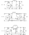
図8は、本実施形態のDC−DCコンバータの等価回路図であり、ここでは、図8(A)〜図8(C)の三種類を例に示しているが、他の構成であってもよい。 FIG. 8 is an equivalent circuit diagram of the DC-DC converter of the present embodiment. Here, three types of FIGS. 8A to 8C are shown as examples, but other configurations are shown. Also good.
図8(A)のDC−DCコンバータは、出力電流値に応じてスイッチング制御を行う非絶縁型の降圧コンバータであり、スイッチ具素子Q1,Q2、出力インダクタLo、平滑用キャパシタCo、出力電流検出用の抵抗素子R1,R2、制御ICを有する。 The DC-DC converter shown in FIG. 8A is a non-insulated step-down converter that performs switching control according to an output current value, and includes switch device elements Q1 and Q2, an output inductor Lo, a smoothing capacitor Co, and an output current detection. Resistance elements R1, R2 and a control IC.
図8(B)のDC−DCコンバータは、出力電流値のみでなく出力インダクタLoの電流検出結果を用いてスイッチング制御を行う非絶縁型の降圧コンバータであり、図8(A)の構成に加えて、出力インダクタLoの電流値を検出するための抵抗器RD、オペアンプOPを有する。 The DC-DC converter of FIG. 8B is a non-insulated step-down converter that performs switching control using not only the output current value but also the current detection result of the output inductor Lo. In addition to the configuration of FIG. The resistor RD for detecting the current value of the output inductor Lo and the operational amplifier OP are provided.
図8(C)のDC−DCコンバータは、出力電流のみでなく出力インダクタLoの電流検出結果を用いてスイッチング制御を行う非絶縁型の降圧コンバータであり、図8(A)の構成に加えて、出力インダクタLoの電流値を取得するための抵抗器RD1とキャパシタCD1との直列回路、およびキャパシタCD2と抵抗器RD2との直列回路を有する。 The DC-DC converter of FIG. 8C is a non-insulated step-down converter that performs switching control using not only the output current but also the current detection result of the output inductor Lo. In addition to the configuration of FIG. And a series circuit of a resistor RD1 and a capacitor CD1 for obtaining a current value of the output inductor Lo, and a series circuit of a capacitor CD2 and a resistor RD2.
これらのようなDC−DCコンバータにおいて、出力インダクタLoが上述の第1実施形態や第2実施形態で示したインダクタにより実現される。そして、他の回路素子および回路パターンが、後述する実装回路基板上に形成された電極パターンおよび実装される実装電子部品SMDにより実現される。このような構成を用いれば、特に、POL(Point of Load)に利用されるDC−DCコンバータの場合、負荷電流が急激に増減し、且つ小型で低背化が要求されるので、以下に示す本実施形態の構成は、より一層有効である。 In such DC-DC converters, the output inductor Lo is realized by the inductors described in the first and second embodiments. Other circuit elements and circuit patterns are realized by an electrode pattern formed on a mounting circuit board to be described later and a mounted electronic component SMD to be mounted. If such a configuration is used, particularly in the case of a DC-DC converter used for POL (Point of Load), the load current increases and decreases rapidly, and a small size and a low profile are required. The configuration of this embodiment is even more effective.
次に、具体的なDC−DCコンバータの機構的構成について示す。図9(A)〜(C)および図10(A),(B)は、本実施形態のDC−DCコンバータの機構的構成を模式的に示す側面図である。
これらのDC−DCコンバータM1〜M5は、基本構造として、2層構造からなり、図示しないマザー基板に、上述の各回路素子が実装された実装回路基板が実装され、当該実装回路基板上に出力インダクタLoとなるインダクタが配置される構造からなる。
Next, a specific mechanical configuration of the DC-DC converter will be described. 9A to 9C and FIGS. 10A and 10B are side views schematically showing the mechanical configuration of the DC-DC converter of the present embodiment.
These DC-DC converters M1 to M5 have a two-layer structure as a basic structure, and a mounting circuit board on which each of the above-described circuit elements is mounted is mounted on a mother board (not shown), and output on the mounting circuit board. It has a structure in which an inductor serving as an inductor Lo is arranged.
図9(A)のDC−DCコンバータM1は、上述の実施形態で示した突起電極106(106A〜106D)を有するインダクタ1Dと、実装回路基板20とを備える。実装回路基板20には、図8(A)〜図8(C)のいずれかを構成するための回路パターンが形成されており、実装面には、接続用ランド電極21、実装用ランド電極22が形成されている。各実装用ランド電極22には、図8(A)〜図8(C)のいずれかを構成する回路素子SMD1〜SMD4が実装されている。また、各接続用ランド電極21には、インダクタ1Dの第1突起電極103および第2突起電極104のそれぞれが接続されている。また、各突起電極106は、図示しない浮き電極に接合されている。このような構成では、第1突起電極103、第2突起電極104、突起電極106がインダクタ1Dを実装回路基板20上の所定位置に支持するための脚として機能する。
The DC-DC converter M1 in FIG. 9A includes the
このような2層構造を用いることで、従来のディスクリート型のインダクタを実装回路基板20の実装面に直接設置して実装するよりも、DC−DCコンバータのマザー基板に対する平面面積を小さくし、省スペース化することができる。さらに、上述の低背化されたインダクタを用いることで、2層構造でありながらもDC−DCコンバータを低背に形成することができる。
By using such a two-layer structure, the plane area of the DC-DC converter with respect to the mother board can be reduced and saved compared with the conventional discrete type inductor mounted directly on the mounting surface of the mounting
図9(B)のDC−DCコンバータM2は、上述の実施形態で示した磁性体突起部115を有するインダクタ1Cと実装回路基板20とを備える。実装回路基板20の構成は、図9(A)と基本的に同じであるが、DC−DCコンバータM2は、磁性体突起部115が実装回路基板20の実装面に当接する構造からなり、当該磁性体突起部115をインダクタ1Cの支持のための脚として用いている。このような構成であっても、省スペースで低背のDC−DCコンバータを形成することができる。さらに、磁性体突起部115の延びる方向に垂直な断面積を大きくすることで、より高い機械的強度を得ることができる。
The DC-DC converter M2 of FIG. 9B includes the
図9(C)のDC−DCコンバータM3は、上述の実施形態で示した基本構成のインダクタ1と実装回路基板20とを備える。実装回路基板20の構成は、図9(A)と同じであるが、DC−DCコンバータM3は、インダクタ1の下部すなわち第1磁性体層11の表面に補強脚30を配置している。この補強脚30は絶縁性材料で所定の機械的強度を有する材料が用いられており、上述の磁性体突起部115と同様に機能を果たす。このような構成であっても、省スペースで低背のDC−DCコンバータを形成することができる。さらに、補強脚30の延びる方向に垂直な断面積を大きくすることで、より高い機械的強度を得ることができる。
The DC-DC converter M3 in FIG. 9C includes the
図10(A)のDC−DCコンバータM4は、図9(C)のDC−DCコンバータM3と同様に、上述の最も単純な構成のインダクタ1と実装回路基板20とを備える。実装回路基板20の基本的構成は、図9(A)と同じであるが、実装回路基板20の実装面上に、第1突起電極103および第2突起電極104の突出部分の長さに準じた誘電体の支持部材25が形成されている。このような構成であっても、省スペースで低背のDC−DCコンバータを形成することができる。さらに、支持部材25の延びる方向に垂直な断面積を大きくすることで、より高い機械的強度を得ることができる。
The DC-DC converter M4 in FIG. 10A includes the
図10(B)のDC−DCコンバータM5は、図9(A)のDC−DCコンバータM1に対して、インダクタ1Dと実装回路基板20との間に絶縁性樹脂等からなるアンダーフィル40を充填させた構成を有する。このような構成であっても、省スペースで低背のDC−DCコンバータを形成することができ、アンダーフィル40により機械的強度を高くすることができる。さらに、アンダーフィル40により、第1突起電極103、第2突起電極104、突起電極106、および回路素子SMD1〜SMD4を外的に保護できるので、より信頼性の高いDC−DCコンバータを形成することができる。
The DC-DC converter M5 of FIG. 10B fills the
なお、これら図9(A)〜(C)、図10(A),(B)の構成は一例であり、これらの構成を適宜組み合わせ、DC−DCコンバータを形成してもよい。 Note that the configurations of FIGS. 9A to 9C and FIGS. 10A and 10B are examples, and these configurations may be appropriately combined to form a DC-DC converter.
次に、第4の実施形態に係るDC−DCコンバータについて図を参照して説明する。
図11は本実施形態のDC−DCコンバータの機構的構成を模式的に示す側面図である。
Next, a DC-DC converter according to a fourth embodiment will be described with reference to the drawings.
FIG. 11 is a side view schematically showing the mechanical configuration of the DC-DC converter of the present embodiment.
これらのDC−DCコンバータM1R,M2Rも、基本構造として2層構造からなるが、図9、図10のDC−DCコンバータと異なり、マザー基板にインダクタ1が配置され、当該インダクタ1上に、各回路素子が実装された実装回路基板が配置される構造を有する。
These DC-DC converters M1R and M2R also have a two-layer structure as a basic structure. However, unlike the DC-DC converters shown in FIGS. 9 and 10, an
図11(A)のDC−DCコンバータM1Rは、マザー基板200上に、上述のインダクタ1が配置される。この際、インダクタ1は、平坦面である第2磁性体層12側がマザー基板200に当接するように配置される。このインダクタ1の第1磁性体層11側の表面には、実装回路基板20が配置される。この際、実装回路基板20は、各回路素子が実装される実装面と反対側の面がインダクタ1の第1磁性体層11に当接するように配置される。実装回路基板20の各回路素子SMD1〜SMD4の実装構成は、上述の図9、図10に示した実装回路基板20と同じであるが、図11(A)の実装回路基板20には、インダクタ1の第1突起電極103および第2突起電極104が、実装面側に露出するための貫通孔(図示せず)が形成されており、当該貫通孔を介して、実装面側の接続用ランド電極21に第1突起電極103および第2突起電極104が接続されている。また、インダクタ1の側面には、図示しない配線電極が形成されており、当該配線電極を介して、実装回路基板20とマザー基板200とが電気的に接続されている。このような構成であっても、省スペースで低背のDC−DCコンバータを形成することができる。
In the DC-DC converter M1R of FIG. 11A, the above-described
図11(B)のDC−DCコンバータM2Rは、図11(A)のDC−DCコンバータM1Rと同様に、マザー基板200上にインダクタ1が直接配置されている。そして、DC−DCコンバータM2Rでは、インダクタ1上に配置される実装回路基板20Aが、インダクタ1から所定距離離間され、且つ実装面がインダクタ1側を向くように配置されている。また、実装回路基板20Aは、平面視した面積が、インダクタ1よりも広く形成されている。インダクタ1と実装回路基板20Aとの電気的な接続や支持構造は上述の図9(A)の構造を天地反転した構造からなり、第1突起電極103および第2突起電極104を接続用ランド電極21に接合することで電気的な接続を実現し、第1突起電極103、第2突起電極104、誘電体の支持部材25により実装回路基板20Aの支持機構を実現している。そして、図11(B)に示すように、実装回路基板20Aがインダクタ1よりも広ければ、インダクタ1を介さない領域における実装回路基板20Aの接続用ランド電極21Tとマザー基板200の接続用ランド電極203とを、導電支柱部材211で接続することで、実装回路基板20Aとマザー基板200との電気的接続を実現している。このような構成であっても、省スペースで低背のDC−DCコンバータを形成することができる。
In the DC-DC converter M2R in FIG. 11B, the
なお、図11(A),(B)に示す構成も一例であり、これらの構成を適宜組み合わせて、DC−DCコンバータを形成してもよい。 Note that the configurations illustrated in FIGS. 11A and 11B are examples, and a DC-DC converter may be formed by appropriately combining these configurations.
1,1A〜1D−インダクタ素子、10,10A,10B−コイル電極部、11,11A〜11C−第1磁性体層、12−第2磁性体層、13−補強材、101−第1スパイラル電極、102−第2スパイラル電極、103,104,106,106A〜106D−突起電極、105−接続電極、110,120−磁性体、110Br,120Br−立体領域、113,114,116A〜116D−貫通孔、115−磁性体突起部、121−凹部、122−凸部、20−実装回路基板、21,21T,203−接続用ランド電極、22−実装用ランド電極、25−支持部材、30−補強脚、40−アンダーフィル、200−マザー基板、211−導電支柱部材
DESCRIPTION OF
Claims (18)
該コイル電極部を挟持し前記第1突起電極および第2突起電極が外部へ露出するように形成された磁性体層と、を備えるインダクタであって、
前記磁性体層は、前記第1スパイラル電極、前記第2スパイラル電極、および前記接続電極を前記平面に直交する方向から挟み込む第1磁性体層と第2磁性体層とからなり、
前記第1磁性体層には、前記突起電極が挿通する貫通孔が形成され、
前記第2磁性体層には、前記第1スパイラル電極、前記第2スパイラル電極、および前記接続電極が収納される凹部が形成されており、該凹部によって、前記第1スパイラル電極および前記第2スパイラル電極の巻回の中央領域において前記第1磁性体層に当接もしくは近接する高さの凸部を備え、
該凸部と、該凸部の平面領域を前記第1磁性体層の厚み方向の全長に亘って仮想的に伸延させた第1の立体領域と、前記凸部の平面領域を該凸部を除き前記第2磁性体層の厚み方向の全長に亘って仮想的に伸延させた第2の立体領域と、からなる領域を中央の立体領域とし、
前記第1スパイラル電極もしくは前記第2スパイラル電極に対応して前記中央の立体領域における前記第1磁性体層もしくは前記凸部を除く前記第2磁性体層を横断する前記厚み方向に平行な側面の面積Svと、前記中央の立体領域の前記第1スパイラル電極もしくは前記第2スパイラル電極の厚み方向の中央断面に沿った断面の面積Shとが、0.1<Sv/Sh<0.65となるように形成されている、ことを特徴とするインダクタ。 Connection electrode connecting the first spiral electrode and a second spiral electrode in the same plane are formed in a spiral shape which is wound in the same direction, and an outer peripheral edge of the outer peripheral end of the second spiral electrode the first spiral electrode , before Symbol in a first direction substantially perpendicular to the plane formed at the inner peripheral end of the protruding electrode and the second spiral electrode extending in a direction substantially perpendicular to the plane formed at the inner peripheral end of the first spiral electrode a coil electrode portion second has a projection electrodes, the pre-Symbol first protruding electrode and the second protruding electrode and across electrodes extending,
An inductor comprising: a magnetic layer formed so as to sandwich the coil electrode portion and expose the first protruding electrode and the second protruding electrode to the outside ,
The magnetic layer is composed of a first magnetic layer and a second magnetic layer that sandwich the first spiral electrode, the second spiral electrode, and the connection electrode from a direction perpendicular to the plane,
A through hole through which the protruding electrode is inserted is formed in the first magnetic layer,
The second magnetic layer is formed with a recess for accommodating the first spiral electrode, the second spiral electrode, and the connection electrode, and the recess forms the first spiral electrode and the second spiral. A convex portion having a height in contact with or close to the first magnetic layer in the central region of the winding of the electrode;
The convex portion, a first three-dimensional region virtually extending the planar region of the convex portion over the entire length of the first magnetic layer, and the planar region of the convex portion Excluding the second three-dimensional region virtually extended over the entire length in the thickness direction of the second magnetic layer, and a region composed of the second three-dimensional region as a central three-dimensional region,
Corresponding to the first spiral electrode or the second spiral electrode, a side surface parallel to the thickness direction crossing the second magnetic layer excluding the first magnetic layer or the convex portion in the central three-dimensional region. The area Sv and the area Sh of the cross section along the central cross section in the thickness direction of the first spiral electrode or the second spiral electrode of the central three-dimensional region satisfy 0.1 <Sv / Sh <0.65. An inductor characterized by being formed as follows .
DC−DCコンバータを構成するための回路パターンが形成され、該回路パターンの所定ランドに少なくともキャパシタとスイッチ素子とを含む複数の電子部品が実装された実装回路基板と、を備え、
前記平板状のインダクタは、該実装回路基板の実装面側に、前記複数の電子部品の少なくとも一部を覆うように配置され、前記回路パターンの出力インダクタが接続されるべきランドに、前記第1突起電極および第2突起電極が接続されており、
前記磁性体層は、前記第1スパイラル電極、前記第2スパイラル電極、および前記接続電極を前記平面に直交する方向から挟み込む第1磁性体層と第2磁性体層とからなり、
前記第1磁性体層には、前記突起電極が挿通する貫通孔が形成され、
前記第2磁性体層には、前記第1スパイラル電極、前記第2スパイラル電極、および前記接続電極が収納される凹部が形成されており、該凹部によって、前記第1スパイラル電極および前記第2スパイラル電極の巻回の中央領域において前記第1磁性体層に当接もしくは近接する高さの凸部を備え、
該凸部と、該凸部の平面領域を前記第1磁性体層の厚み方向の全長に亘って仮想的に伸延させた第1の立体領域と、前記凸部の平面領域を該凸部を除き前記第2磁性体層の厚み方向の全長に亘って仮想的に伸延させた第2の立体領域と、からなる領域を中央の立体領域とし、
前記第1スパイラル電極もしくは前記第2スパイラル電極に対応して前記中央の立体領域における前記第1磁性体層もしくは前記凸部を除く前記第2磁性体層を横断する前記厚み方向に平行な側面の面積Svと、前記中央の立体領域の前記第1スパイラル電極もしくは前記第2スパイラル電極の厚み方向の中央断面に沿った断面の面積Shとが、0.1<Sv/Sh<0.65となるように形成されている、ことを特徴とするDC−DCコンバータ。 Connection electrode connecting the first spiral electrode and a second spiral electrode in the same plane are formed in a spiral shape which is wound in the same direction, and an outer peripheral edge of the outer peripheral end of the second spiral electrode the first spiral electrode , before Symbol in a first direction substantially perpendicular to the plane formed at the inner peripheral end of the protruding electrode and the second spiral electrode extending in a direction substantially perpendicular to the plane formed at the inner peripheral end of the first spiral electrode extending the second has a projection electrodes, before Symbol a coil electrode portion and the first protruding electrode and the second electrodes at both ends of the protruding electrodes, the coil electrode portion is sandwiched the first protruding electrode and the second protruding electrode external A magnetic layer formed so as to be exposed to a flat plate-shaped inductor that has a spread along the plane and is thin in the thickness direction perpendicular to the plane;
A circuit pattern for forming a DC-DC converter is formed, and a mounting circuit board on which a plurality of electronic components including at least a capacitor and a switch element are mounted on a predetermined land of the circuit pattern,
The flat inductor is disposed on the mounting surface side of the mounting circuit board so as to cover at least a part of the plurality of electronic components, and the first inductor is connected to a land to which the output inductor of the circuit pattern is to be connected. The protruding electrode and the second protruding electrode are connected ,
The magnetic layer is composed of a first magnetic layer and a second magnetic layer that sandwich the first spiral electrode, the second spiral electrode, and the connection electrode from a direction perpendicular to the plane,
A through hole through which the protruding electrode is inserted is formed in the first magnetic layer,
The second magnetic layer is formed with a recess for accommodating the first spiral electrode, the second spiral electrode, and the connection electrode, and the recess forms the first spiral electrode and the second spiral. A convex portion having a height in contact with or close to the first magnetic layer in the central region of the winding of the electrode;
The convex portion, a first three-dimensional region virtually extending the planar region of the convex portion over the entire length of the first magnetic layer, and the planar region of the convex portion Excluding the second three-dimensional region virtually extended over the entire length in the thickness direction of the second magnetic layer, and a region composed of the second three-dimensional region as a central three-dimensional region,
Corresponding to the first spiral electrode or the second spiral electrode, a side surface parallel to the thickness direction crossing the second magnetic layer excluding the first magnetic layer or the convex portion in the central three-dimensional region. The area Sv and the area Sh of the cross section along the central cross section in the thickness direction of the first spiral electrode or the second spiral electrode of the central three-dimensional region satisfy 0.1 <Sv / Sh <0.65. A DC-DC converter characterized by being formed as described above .
該更なる突起電極の少なくとも1個は、前記実装回路基板の前記回路パターンにおける前記出力インダクタの中間タップとなる位置に接続されている、
請求項10または請求項11に記載のDC−DCコンバータ。 The coil electrode portion of the flat inductor has a further protruding electrode having a shape extending in the same direction as the first protruding electrode and the second protruding electrode,
At least one of the further protruding electrodes is connected to a position to be an intermediate tap of the output inductor in the circuit pattern of the mounting circuit board.
The DC-DC converter according to claim 10 or 11 .
該更なる突起電極は、前記平板状のインダクタと前記実装回路基板との距離と略同じ長さで形成され、前記実装回路基板の浮き電極に接続されている、
請求項10〜請求項12のいずれかに記載のDC−DCコンバータ。 The coil electrode portion of the flat inductor has a further protruding electrode having a shape extending in the same direction as the first protruding electrode and the second protruding electrode,
The further protruding electrode is formed with a length substantially the same as the distance between the flat inductor and the mounting circuit board, and is connected to the floating electrode of the mounting circuit board.
The DC-DC converter in any one of Claims 10-12 .
前記平板状のインダクタを間に介さない領域に前記実装回路基板を前記マザー基板に接続する接続手段を備える、請求項10〜請求項15のいずれかに記載のDC−DCコンバータ。 With respect to the mother board on which the DC-DC converter is mounted, the planar inductor and the mounting circuit board are arranged in this order from the mother board side, and the area of the mounting circuit board projected onto the mother board Has a shape wider than the area of the plate-shaped inductor,
The DC-DC converter according to any one of claims 10 to 15 , further comprising a connection unit that connects the mounting circuit board to the mother board in a region that does not interpose the flat inductor.
Priority Applications (4)
| Application Number | Priority Date | Filing Date | Title |
|---|---|---|---|
| JP2009199133A JP5084801B2 (en) | 2009-08-31 | 2009-08-31 | Inductor and DC-DC converter |
| CN201010263838.1A CN102005279B (en) | 2009-08-31 | 2010-08-25 | Inductor and dc-dc converter |
| DE102010035388A DE102010035388A1 (en) | 2009-08-31 | 2010-08-25 | Inductor and DC-DC converter |
| US12/870,889 US8284010B2 (en) | 2009-08-31 | 2010-08-30 | Inductor and DC-DC converter |
Applications Claiming Priority (1)
| Application Number | Priority Date | Filing Date | Title |
|---|---|---|---|
| JP2009199133A JP5084801B2 (en) | 2009-08-31 | 2009-08-31 | Inductor and DC-DC converter |
Publications (2)
| Publication Number | Publication Date |
|---|---|
| JP2011054585A JP2011054585A (en) | 2011-03-17 |
| JP5084801B2 true JP5084801B2 (en) | 2012-11-28 |
Family
ID=43623879
Family Applications (1)
| Application Number | Title | Priority Date | Filing Date |
|---|---|---|---|
| JP2009199133A Active JP5084801B2 (en) | 2009-08-31 | 2009-08-31 | Inductor and DC-DC converter |
Country Status (4)
| Country | Link |
|---|---|
| US (1) | US8284010B2 (en) |
| JP (1) | JP5084801B2 (en) |
| CN (1) | CN102005279B (en) |
| DE (1) | DE102010035388A1 (en) |
Families Citing this family (34)
| Publication number | Priority date | Publication date | Assignee | Title |
|---|---|---|---|---|
| WO2007132558A1 (en) * | 2006-05-11 | 2007-11-22 | Tamura Corporation | Coil and coil shaping method |
| JP5605153B2 (en) | 2010-10-15 | 2014-10-15 | ソニー株式会社 | Power supply device, power supply method, and power supply system |
| JP5625723B2 (en) * | 2010-10-15 | 2014-11-19 | ソニー株式会社 | Electronic device, power supply method and power supply system |
| JP5195876B2 (en) * | 2010-11-10 | 2013-05-15 | Tdk株式会社 | Coil component and manufacturing method thereof |
| US9767947B1 (en) | 2011-03-02 | 2017-09-19 | Volterra Semiconductor LLC | Coupled inductors enabling increased switching stage pitch |
| JP5736949B2 (en) * | 2011-05-13 | 2015-06-17 | 株式会社村田製作所 | High frequency circuit module |
| JP5898875B2 (en) * | 2011-07-22 | 2016-04-06 | ミネベア株式会社 | DC-DC converter |
| US9263177B1 (en) * | 2012-03-19 | 2016-02-16 | Volterra Semiconductor LLC | Pin inductors and associated systems and methods |
| US9083332B2 (en) | 2012-12-05 | 2015-07-14 | Volterra Semiconductor Corporation | Integrated circuits including magnetic devices |
| JP6353642B2 (en) * | 2013-02-04 | 2018-07-04 | 株式会社トーキン | Magnetic core, inductor, and module with inductor |
| US9287038B2 (en) | 2013-03-13 | 2016-03-15 | Volterra Semiconductor LLC | Coupled inductors with non-uniform winding terminal distributions |
| JP2014212688A (en) * | 2013-04-19 | 2014-11-13 | サムソン エレクトロ−メカニックス カンパニーリミテッド. | Composite electronic component, packaging substrate thereof, and power supply stabilization unit including the same |
| JP5773102B2 (en) * | 2013-05-14 | 2015-09-02 | 株式会社村田製作所 | Inductor simulation method, inductor simulation apparatus and method of using the same |
| US9564264B2 (en) * | 2013-08-30 | 2017-02-07 | Virginia Tech Intellectual Properties, Inc. | High frequency integrated point-of-load power converter with embedded inductor substrate |
| KR101983149B1 (en) | 2013-09-24 | 2019-05-28 | 삼성전기주식회사 | Laminated Inductor And Manufacturing Method Thereof |
| JP6227446B2 (en) * | 2014-03-12 | 2017-11-08 | 日立オートモティブシステムズ株式会社 | Transformer and power converter using the same |
| US20150279548A1 (en) | 2014-04-01 | 2015-10-01 | Virginia Tech Intellectual Properties, Inc. | Compact inductor employing redistrubuted magnetic flux |
| KR102080659B1 (en) * | 2014-09-16 | 2020-02-24 | 삼성전기주식회사 | Coil component and and board for mounting the same |
| CN107408449B (en) * | 2015-03-16 | 2019-03-05 | 三菱电机株式会社 | Insulating transformer |
| WO2016203804A1 (en) * | 2015-06-19 | 2016-12-22 | 株式会社村田製作所 | Dc-dc converter |
| CN106571732B (en) * | 2015-10-09 | 2019-03-05 | 台达电子工业股份有限公司 | Power supply conversion device |
| CN112259341A (en) * | 2015-10-26 | 2021-01-22 | 鲲腾科技有限公司 | Magnetic structure with self-closing magnetic circuit |
| US10034379B2 (en) * | 2016-01-29 | 2018-07-24 | Cyntec Co., Ltd. | Stacked electronic structure |
| CN107046366B (en) | 2016-02-05 | 2019-06-04 | 台达电子企业管理(上海)有限公司 | Supply convertor and preparation method thereof |
| JP6693228B2 (en) * | 2016-03-30 | 2020-05-13 | Tdk株式会社 | Electronic component mounting board |
| US10438889B2 (en) * | 2016-12-23 | 2019-10-08 | Advanced Semiconductor Engineering, Inc. | Semiconductor package device and method of manufacturing the same |
| KR102369430B1 (en) * | 2017-03-15 | 2022-03-03 | 삼성전기주식회사 | Coil electronic component and board having the same |
| JP6828555B2 (en) | 2017-03-29 | 2021-02-10 | Tdk株式会社 | Coil parts and their manufacturing methods |
| US10461696B2 (en) | 2017-10-23 | 2019-10-29 | Analog Devices, Inc. | Switched capacitor banks |
| US10469029B2 (en) | 2017-10-23 | 2019-11-05 | Analog Devices, Inc. | Inductor current distribution |
| CN112236928B (en) * | 2018-08-17 | 2024-08-09 | 株式会社村田制作所 | Switching power supply device |
| US11127524B2 (en) * | 2018-12-14 | 2021-09-21 | Hong Kong Applied Science and Technology Research Institute Company Limited | Power converter |
| WO2024053620A1 (en) * | 2022-09-05 | 2024-03-14 | 大日本印刷株式会社 | Coil component, manufacturing method for same, power transmission device, power reception device, power transmission system, and mobile body |
| WO2024090418A1 (en) * | 2022-10-27 | 2024-05-02 | 株式会社村田製作所 | Switching power supply system device comprising planar-array inductor |
Family Cites Families (37)
| Publication number | Priority date | Publication date | Assignee | Title |
|---|---|---|---|---|
| NZ207264A (en) * | 1984-02-23 | 1988-10-28 | New Zealand Dev Finance | Flexible printed circuit coil |
| JPS61203528U (en) * | 1985-06-11 | 1986-12-22 | ||
| JPS63155606U (en) | 1987-03-31 | 1988-10-12 | ||
| JPH01157507A (en) | 1987-09-29 | 1989-06-20 | Toshiba Corp | Plane inductor |
| US5111169A (en) * | 1989-03-23 | 1992-05-05 | Takeshi Ikeda | Lc noise filter |
| JPH0722241A (en) | 1993-07-05 | 1995-01-24 | Matsushita Electric Ind Co Ltd | Planar inductor and production thereof |
| JP2714343B2 (en) * | 1993-07-30 | 1998-02-16 | コーア株式会社 | High frequency coil and method of manufacturing the same |
| JP3027081B2 (en) * | 1993-12-09 | 2000-03-27 | アルプス電気株式会社 | Thin film element |
| JPH07326518A (en) * | 1994-05-31 | 1995-12-12 | Nemitsuku Ramuda Kk | Inductance element |
| DE4446369A1 (en) * | 1994-12-23 | 1996-06-27 | Giesecke & Devrient Gmbh | Data carrier with an electronic module |
| JP3410876B2 (en) * | 1995-09-14 | 2003-05-26 | 株式会社東芝 | Planar inductors, electronic components mounted with planar inductors |
| JP3269371B2 (en) * | 1996-02-08 | 2002-03-25 | 松下電器産業株式会社 | Sheet transformer |
| JPH10150337A (en) * | 1996-11-19 | 1998-06-02 | Ngk Spark Plug Co Ltd | Reflection characteristic adjustment method for lc low pass filter |
| JP3250503B2 (en) * | 1997-11-11 | 2002-01-28 | 株式会社村田製作所 | Variable inductor element |
| JP3368871B2 (en) * | 1999-07-23 | 2003-01-20 | 松下電器産業株式会社 | Inductor component and manufacturing method thereof |
| US6097273A (en) * | 1999-08-04 | 2000-08-01 | Lucent Technologies Inc. | Thin-film monolithic coupled spiral balun transformer |
| JP2001143930A (en) | 1999-11-15 | 2001-05-25 | Alps Electric Co Ltd | Thin film magnetic element |
| JP2001196226A (en) * | 2000-01-12 | 2001-07-19 | Taiyo Yuden Co Ltd | Inductor and manufacturing method thereof |
| JP2001244123A (en) * | 2000-02-28 | 2001-09-07 | Kawatetsu Mining Co Ltd | Surface-mounted planar magnetic element and method of manufacturing |
| JP2001267155A (en) | 2000-03-17 | 2001-09-28 | Fuji Electric Co Ltd | Planar magnetic element |
| JP3435636B2 (en) * | 2000-04-06 | 2003-08-11 | 株式会社村田製作所 | Variable inductance element |
| US6380821B1 (en) * | 2000-08-24 | 2002-04-30 | International Business Machines Corporation | Substrate shielded multilayer balun transformer |
| JP2002175922A (en) * | 2000-12-08 | 2002-06-21 | Sansha Electric Mfg Co Ltd | High-frequency large current transformer |
| US6587025B2 (en) * | 2001-01-31 | 2003-07-01 | Vishay Dale Electronics, Inc. | Side-by-side coil inductor |
| JP4711593B2 (en) * | 2002-06-07 | 2011-06-29 | Jfeスチール株式会社 | Planar magnetic element |
| US6683510B1 (en) * | 2002-08-08 | 2004-01-27 | Northrop Grumman Corporation | Ultra-wideband planar coupled spiral balun |
| JP2004343976A (en) | 2003-03-14 | 2004-12-02 | Fuji Electric Holdings Co Ltd | Multi-output microminiature power conversion device |
| JP2005217234A (en) * | 2004-01-30 | 2005-08-11 | Nec Tokin Corp | Power supply control circuit block for lsi module |
| WO2005117037A1 (en) * | 2004-05-28 | 2005-12-08 | Matsushita Electric Industrial Co., Ltd. | Common mode noise filter |
| JP2006114792A (en) * | 2004-10-18 | 2006-04-27 | Fuji Electric Device Technology Co Ltd | Ultra-compact power converter |
| US7262684B2 (en) * | 2004-10-29 | 2007-08-28 | Lear Corporation | Efficient RKE energy monitoring strategy |
| JP2006286884A (en) * | 2005-03-31 | 2006-10-19 | Tdk Corp | Common mode choke coil |
| WO2007069403A1 (en) * | 2005-12-16 | 2007-06-21 | Murata Manufacturing Co., Ltd. | Composite transformer and insulated switching power supply |
| JP2007250924A (en) * | 2006-03-17 | 2007-09-27 | Sony Corp | Inductor element, manufacturing method thereof, and semiconductor module using inductor element |
| JP2008041973A (en) * | 2006-08-08 | 2008-02-21 | Sumida Corporation | Low profile inductor |
| JP2008108936A (en) * | 2006-10-26 | 2008-05-08 | Densei Lambda Kk | Transformer structure |
| JP2008135430A (en) * | 2006-11-27 | 2008-06-12 | Matsushita Electric Ind Co Ltd | High-frequency module |
-
2009
- 2009-08-31 JP JP2009199133A patent/JP5084801B2/en active Active
-
2010
- 2010-08-25 CN CN201010263838.1A patent/CN102005279B/en active Active
- 2010-08-25 DE DE102010035388A patent/DE102010035388A1/en not_active Withdrawn
- 2010-08-30 US US12/870,889 patent/US8284010B2/en active Active
Also Published As
| Publication number | Publication date |
|---|---|
| CN102005279A (en) | 2011-04-06 |
| US20110050191A1 (en) | 2011-03-03 |
| JP2011054585A (en) | 2011-03-17 |
| DE102010035388A1 (en) | 2011-07-07 |
| CN102005279B (en) | 2012-12-12 |
| US8284010B2 (en) | 2012-10-09 |
Similar Documents
| Publication | Publication Date | Title |
|---|---|---|
| JP5084801B2 (en) | Inductor and DC-DC converter | |
| JP4802615B2 (en) | LC composite parts | |
| CN1881488B (en) | Magnetic element | |
| US8373534B2 (en) | Flexible coil | |
| JP4548522B2 (en) | Coil component and power supply device including the same | |
| JP4140632B2 (en) | Multiple choke coil and electronic device using the same | |
| JP4354472B2 (en) | Electronic component module | |
| JP2007503715A (en) | Printed circuit board with integrated inductor | |
| JP6624160B2 (en) | Transformer integrated printed circuit board | |
| KR20150081834A (en) | Coil component and and board for mounting the same | |
| JP2008060427A (en) | Passive component and electronic component module | |
| JP2009049046A (en) | Electronic component module | |
| CN108701527B (en) | Inductor component and method for manufacturing inductor component | |
| JP2010232314A (en) | Electronic component module | |
| JP6610769B2 (en) | Electronic component module, DC-DC converter, and electronic device | |
| JP3141709U (en) | Coil parts | |
| JP7268611B2 (en) | inductor components | |
| JP3623720B2 (en) | Thin inductor | |
| JP4802616B2 (en) | LC composite parts | |
| JP4985852B2 (en) | Mounted electronic circuit module | |
| JP7302276B2 (en) | inductor | |
| KR20190014727A (en) | Dual Core Planar Transformer | |
| JP6439289B6 (en) | Winding parts and power supply | |
| CN113284713A (en) | Coil device | |
| JP5233791B2 (en) | Electronic component module |
Legal Events
| Date | Code | Title | Description |
|---|---|---|---|
| A621 | Written request for application examination |
Free format text: JAPANESE INTERMEDIATE CODE: A621 Effective date: 20110518 |
|
| A977 | Report on retrieval |
Free format text: JAPANESE INTERMEDIATE CODE: A971007 Effective date: 20111007 |
|
| A131 | Notification of reasons for refusal |
Free format text: JAPANESE INTERMEDIATE CODE: A131 Effective date: 20111025 |
|
| A521 | Request for written amendment filed |
Free format text: JAPANESE INTERMEDIATE CODE: A523 Effective date: 20111219 |
|
| TRDD | Decision of grant or rejection written | ||
| A01 | Written decision to grant a patent or to grant a registration (utility model) |
Free format text: JAPANESE INTERMEDIATE CODE: A01 Effective date: 20120807 |
|
| A01 | Written decision to grant a patent or to grant a registration (utility model) |
Free format text: JAPANESE INTERMEDIATE CODE: A01 |
|
| A61 | First payment of annual fees (during grant procedure) |
Free format text: JAPANESE INTERMEDIATE CODE: A61 Effective date: 20120904 |
|
| R150 | Certificate of patent or registration of utility model |
Ref document number: 5084801 Country of ref document: JP Free format text: JAPANESE INTERMEDIATE CODE: R150 Free format text: JAPANESE INTERMEDIATE CODE: R150 |
|
| FPAY | Renewal fee payment (event date is renewal date of database) |
Free format text: PAYMENT UNTIL: 20150914 Year of fee payment: 3 |
|
| R250 | Receipt of annual fees |
Free format text: JAPANESE INTERMEDIATE CODE: R250 |
|
| R250 | Receipt of annual fees |
Free format text: JAPANESE INTERMEDIATE CODE: R250 |
|
| R250 | Receipt of annual fees |
Free format text: JAPANESE INTERMEDIATE CODE: R250 |
|
| R250 | Receipt of annual fees |
Free format text: JAPANESE INTERMEDIATE CODE: R250 |
|
| R250 | Receipt of annual fees |
Free format text: JAPANESE INTERMEDIATE CODE: R250 |
|
| R250 | Receipt of annual fees |
Free format text: JAPANESE INTERMEDIATE CODE: R250 |
|
| R250 | Receipt of annual fees |
Free format text: JAPANESE INTERMEDIATE CODE: R250 |
|
| R250 | Receipt of annual fees |
Free format text: JAPANESE INTERMEDIATE CODE: R250 |
|
| R250 | Receipt of annual fees |
Free format text: JAPANESE INTERMEDIATE CODE: R250 |
|
| R250 | Receipt of annual fees |
Free format text: JAPANESE INTERMEDIATE CODE: R250 |