JP5082418B2 - Information processing system with drive devices connected by FC-AL - Google Patents
Information processing system with drive devices connected by FC-AL Download PDFInfo
- Publication number
- JP5082418B2 JP5082418B2 JP2006332796A JP2006332796A JP5082418B2 JP 5082418 B2 JP5082418 B2 JP 5082418B2 JP 2006332796 A JP2006332796 A JP 2006332796A JP 2006332796 A JP2006332796 A JP 2006332796A JP 5082418 B2 JP5082418 B2 JP 5082418B2
- Authority
- JP
- Japan
- Prior art keywords
- port bypass
- bypass circuit
- loop
- port
- pbc
- Prior art date
- Legal status (The legal status is an assumption and is not a legal conclusion. Google has not performed a legal analysis and makes no representation as to the accuracy of the status listed.)
- Expired - Fee Related
Links
Images


Landscapes
- Debugging And Monitoring (AREA)
- Small-Scale Networks (AREA)
Description
本発明は,複数のハードディスクドライブを備えたRAID(Redundant Arrays of Independent Disks)装置等のドライブ装置をFC−AL(Fibre Channel Arbitrated Loop)により接続した情報処理システムに関する。 The present invention relates to an information processing system in which drive devices such as RAID (Redundant Arrays of Independent Disks) devices having a plurality of hard disk drives are connected by FC-AL (Fibre Channel Arbitrated Loop).
ファイバチャネル(Fibre Channel:FCと略称される) は超高速ギガビット・ネットワーク技術の一つとして知られており,FC−AL(FC Arbitrated Loop: ファイバチャネル調停ループ)のようなループ状にデバイスが接続されるインタフェースが複数のハードディスクを接続してRAID装置を構築する技術として採用されている。 Fiber Channel (abbreviated as FC) is known as one of ultra-high-speed gigabit network technologies, and devices are connected in a loop like FC-AL (FC Arbitrated Loop). Interface is used as a technique for connecting a plurality of hard disks to construct a RAID device.
図12はFC−AL(Fibre Channel Arbitrated Loop:ファイバチャネル調停ループ)のトポロジを示す。図中,50は制御側のイニシエータ(または制御装置),51は複数のターゲット・デバイス(ハードディスク等のドライブ装置)をループ状に接続したFC−AL,52−1〜52−nはポートバイパス回路(PBCと略称される),53−1〜53−nはハードディスク等のターゲットデバイスである。ポートバイパス回路(PBC)52−1,52−nは,それぞれのターゲットデバイス53−1,53−nが正常な状態であると,図に示すように内部のスイッチがターゲットデバイスに向かって入力し,ターゲットデバイスからの出力を隣接するターゲットデバイスへ向かって出力するよう切り替えられている。また,ターゲットデバイス53−2のようにターゲットデバイスの故障が検出されると,対応するポートバイパス回路52−2はターゲットデバイス53−2をバイパスするよう切り替えられる。これにより,他のターゲットデバイスはイニシエータ50からアクセスすることが可能となる。なお,FC−ALは,127台までのデバイスが接続可能であり,デバイス間はリング状に結ばれている。
FIG. 12 shows the topology of FC-AL (Fibre Channel Arbitrated Loop). In the figure, 50 is an initiator (or control device) on the control side, 51 is an FC-AL in which a plurality of target devices (drive devices such as hard disks) are connected in a loop, and 52-1 to 52-n are port bypass circuits. (Abbreviated as PBC), 53-1 to 53-n are target devices such as hard disks. When the target devices 53-1 and 53-n are in a normal state, the port bypass circuits (PBC) 52-1 and 52-n input the internal switches toward the target devices as shown in the figure. , The output from the target device is switched to output to the adjacent target device. When a failure of the target device is detected as in the target device 53-2, the corresponding port bypass circuit 52-2 is switched to bypass the target device 53-2. As a result, other target devices can be accessed from the
図12において,イニシエータ(または制御装置)50からの指令(コマンド)は,FC−AL51の信号伝送方向(一方の方向)に沿って伝送される。正常なターゲットデバイスにそれぞれのポートバイパス回路を介して供給され,宛て先のターゲットデバイスで受け取られて,指令を実行し,処理結果はFC−ALのループの一方向の伝送路を通ってイニシエータ50に供給される。
In FIG. 12, a command (command) from the initiator (or control device) 50 is transmitted along the signal transmission direction (one direction) of the FC-AL 51. A normal target device is supplied via each port bypass circuit, is received by the destination target device, executes a command, and the processing result is sent to the
上記の構成では,ターゲットデバイスが故障した場合に,対応して設けられたポートバイパス回路(PBC)をバスパスするよう切り替えることにより対応することができるが,ポートバイパス回路(PBC)を実現する素子自身が故障したり,エンクロージャ間のケーブル等が故障した場合,リング状のトポロジであるFC−ALでは,同一経路上のデバイス間での通信が不可能となる。 In the above configuration, when the target device fails, the corresponding port bypass circuit (PBC) can be coped with by switching so as to pass the bus. However, the element itself realizing the port bypass circuit (PBC) In the case of a failure or a cable between enclosures or the like, the ring topology FC-AL makes it impossible to communicate between devices on the same path.
すなわち,図12に示すポートバイパス回路52−2の素子自身が故障すると,イニシエータ50から一つ目のターゲットデバイス53−1への送信はできても,そのターゲットデバイス53−1からイニシエータ50に対して送信することは,送信方向に存在するポートバイパス回路52−2が故障しているためにできない。また,送信個所以降については,ターゲットデバイスからイニシエータ50への送信が可能であるが,イニシエータ50からターゲットデバイスへの送信ができなくなる。FC−ALでは,最大127デバイスが接続されるため,1部品の故障で127デバイスの通信が不可能となる。
That is, when the element itself of the port bypass circuit 52-2 shown in FIG. 12 fails, even if transmission from the
これに対応するため,リングを二重化する方法があり,図13は二重化されたFC−ALによるRAID装置の構成例である。図中,60は制御装置の箱を表すコントローラエンクロージャ(Controller Enclosure:CE),61−1は第1のFC−AL,61−2は第2のFC−AL,62(♯1〜♯3)は複数のハードディスク(HDD)を含む箱を表すドライブエンクロージャ(Drive Enclosure :DE),63は第1のポートバイパス回路(PBC♯1−1,♯2−1,♯3−1),64はハードディスク(HDD),65は第2のポートバイパス回路(PBC♯1−2,♯2−2,♯3−2)である。各ドライブエンクロージャ62(♯1〜♯3)内の第1のポートバイパス回路63及び第2のポートバイパス回路65は何れも,上記図12に示す複数のターゲットデバイス53−1〜53−nを順番に接続(またはバイパス)するポートバイパス回路52−1〜52−nと同じ構成を備えている。
In order to cope with this, there is a method of duplexing the ring, and FIG. 13 shows a configuration example of a RAID device based on the duplexed FC-AL. In the figure, 60 is a controller enclosure (CE) representing a box of the control device, 61-1 is a first FC-AL, 61-2 is a second FC-AL, 62 (# 1 to # 3). Is a drive enclosure (Drive Enclosure: DE) representing a box including a plurality of hard disks (HDD), 63 is a first port bypass circuit (PBC # 1-1, # 2-1, # 3-1), and 64 is a hard disk (HDD) 65 is a second port bypass circuit (PBC # 1-2, # 2-2, # 3-2). Each of the first
図13の構成では,コントローラエンクロージャ60からドライブエンクロージャ62♯1の第1のポートバイパス回路63(PBC♯1−1)を介して複数のハードディスクにアクセスし,第1のFC−AL61−1を介してドライブエンクロージャ62♯2の第1のポートバイパス回路(PBC♯2−1)を介して複数のハードディスク64にアクセスし,更に第1のポートバイパス回路63(PBC♯2−1)から第1のFC−AL61−1を通ってドライブエンクロージャ62♯3の第1のポートバイパス回路63(PBC♯3−1)に接続して,第1のループが形成される。
In the configuration of FIG. 13, a plurality of hard disks are accessed from the
また,コントローラエンクロージャ60からドライブエンクロージャ62♯1の第2のポートバイパス回路65(PBC♯1−2)を介して複数のハードディスクにアクセスし,第2のFC−AL61−2を介してドライブエンクロージャ62♯2の第2のポートバイパス回路65(PBC♯2−2)を介して複数のハードディスク64にアクセスし,更に第2のポートバイパス回路65(PBC♯2−2)から第2のFC−AL61−2を通ってドライブエンクロージャ62♯3の第2のポートバイパス回路65(PBC♯3−2)に接続して,第2のループが形成される。
Further, a plurality of hard disks are accessed from the
上記図13に示すようなFC−ALのリングを二重化した場合でも,一方のリングを構成する一部のポートバイパス回路自身に故障が発生することにより,そのリングを介したハードディスクとコントローラエンクロージャ間の双方向の通信ができなくなると,他方のリングを使用した通信しかできなくなり,冗長性が失われて信頼性が低下するという問題がある。更に,通常は,二重化したリングを用いて,負荷分散(例えば,各リングによりアクセスするハードディスクが半分ずつ割り当てる等による)が図られているが,一方への集約により性能的にも半減してしまう。 Even when the FC-AL ring shown in FIG. 13 is duplicated, a failure occurs in a part of the port bypass circuit itself that constitutes one of the rings. When bi-directional communication becomes impossible, only communication using the other ring is possible, and there is a problem that redundancy is lost and reliability is lowered. Furthermore, load sharing (for example, by allocating half of the hard disk accessed by each ring) is usually performed using a duplicated ring, but the performance is halved by consolidating to one side. .
一方,FC−ALのループ状通信手段を備えたシステムにおける障害発生時の性能や信頼性の低下を最小限に止める技術が提案されている(特許文献1参照)。特許文献1の構成を従来のFC−ALのシステム構成として図14に示す。図中,70,71はコントローラ,72〜75はドライブ,76〜87はコントローラまたはドライブに対応したPBC(ポートバイパス回路),88〜93はFCループの中に横断的なバスパスを形成するPBC,94,95は2つのFCループである。
On the other hand, a technique for minimizing degradation in performance and reliability when a failure occurs in a system including FC-AL loop communication means has been proposed (see Patent Document 1). The configuration of
このシステムでは,複数のコントローラ70,71と複数のドライブ72〜75を,複数のFCループ94,95を介して接続し,個々のコントローラ及びドライブのFCループ94,95を個別に制御するPBC76〜81及びPBC82〜87の他に,FCループ94,95をその経路の途中で短絡させるPBC88〜90及びPBC91〜93を設け,PBC88〜90及びPBC91〜93の何れかの選択した位置でFCループ94,95をバイパスさせることで,FCループの中の障害部位を識別し,識別した障害部位を部分的に切り離してFCループの使用を継続させている。
In this system, a plurality of
図14に示す技術によると,各ドライブ毎に自身をバイパスするポートバイパス回路(PBC)の他にループを折り返すためのポートバイパス回路(PBC)がそれぞれ2個ずつ設ける必要があり,多くのドライブ(最大127台)を備えた場合,大量のPBCが必要であるという問題がある。 According to the technique shown in FIG. 14, in addition to the port bypass circuit (PBC) that bypasses itself for each drive, it is necessary to provide two port bypass circuits (PBC) for turning back the loop. When a maximum of 127) is provided, there is a problem that a large amount of PBC is required.
なお,FC−ALのインタフェースを用いたシステムにおいて故障デバイスの切断個所を特定する従来技術として特許文献2を挙げることができる。
上記したように,従来のFC−ALの技術では,ポートバイパス回路自身の故障に対して効率良く信頼性の低下を防止することができないという問題があった。また,FC−ALの技術において,ドライブ装置間のケーブルに障害が発生した時も通信ができないという問題があった。 As described above, the conventional FC-AL technology has a problem in that it cannot efficiently prevent a decrease in reliability against a failure of the port bypass circuit itself. Further, in the FC-AL technology, there is a problem that communication is not possible even when a failure occurs in the cable between the drive devices.
本発明は多数のハードディスクを備えたRAID装置等のドライブ装置をFC−ALにより接続した情報処理システムにおいてFC−ALを構成するポートバイパス回路の部品故障や,FC−ALを構成するケーブルの障害による影響を低減することを目的とする。 The present invention is due to a failure of a part of a port bypass circuit constituting the FC-AL or a failure of a cable constituting the FC-AL in an information processing system in which drive devices such as a RAID device having a large number of hard disks are connected by the FC-AL. The purpose is to reduce the impact.
図1は本発明の第1の原理構成を示す。 FIG. 1 shows a first principle configuration of the present invention.
図中,1は複数のハードディスクを含むFC−ALにより接続された一つの段(この例では2段目として♯2で表す)を構成し,本発明によるポートバイパス回路(PBC)を含むドライブ装置(ドライブエンクロージャと同じ),10は後述する複数のハードディスク12に対応して設けられた第1のポートバイパス回路11に対して1個設けられた第2のポートバイパス回路(PBC♯2−2),11は後述する複数のハードディスク12のそれぞれに対応して設けられたポートバイパス素子(PBCで表す)11a〜11cが順次接続することにより構成された第1のポートバイパス回路(PBC♯2−1),12は複数のハードディスク,2a,2b及び2c,2dはFC−ALのループを構成するケーブルであり,2a,2bは上流側(コントロール側に近い上位のドライブ装置であり,この例では1段のドライブ装置♯1側)に接続するループのケーブル,2c,2dは下流側(この例では後段である図示省略された第3段のドライブ装置♯3側)に接続するループのケーブルである。なお,第1のポートバイパス回路11及び第2のポートバイパス回路10とハードディスク12を含むドライブ装置♯1(図示省略)は上記図12のイニシエータまたは図13のコントローラエンクロージャ(制御装置)と接続され,ハードディスクに対するアクセスやFC−AL等の各種の制御を行う。
In the figure,
図1において,複数のハードディスク12のそれぞれに対応して設けられた複数個のPBC素子を含む第1のポートバイパス回路11(PBC♯2−1)の内部において,一つのPBC素子自身に障害が発生したことが検出されると,第1のポートバイパス回路11内の各ハードディスクに対応するPBC素子を制御して対応することが困難であるため,このドライブ装置1のハードディスクを使用することができない。この時,FC−ALのループを切断されるが,前段と後段のFC−ALを接続するため,第1のポートバイパス回路11のPBC自身に障害が発生したことが検出されると,第2のポートバイパス回路10の切替えを実行して,ケーブル2aと2dを接続する(ケーブル2bと2cは固定接続)。これにより,ドライブ装置1(♯2)は上流側のドライブ装置♯1と下流側のドライブ装置♯3とを直接接続するようバイパスを行い,FC−ALによる他のドライブ装置(♯1,♯3,♯4・・)との通信が継続して実行することができる。
In FIG. 1, in the first port bypass circuit 11 (PBC # 2-1) including a plurality of PBC elements provided corresponding to each of the plurality of
図1の構成では,ドライブ装置1にハードディスク12が設けられた例を示すが,その他の記憶装置を設けることができることはいうまでもなく,後述する図2,図3の構成についても同様である。
1 shows an example in which the
図2は本発明の第2の原理構成を示す。図中,3は複数のハードディスクを含むFC−ALにより接続された一つの段(この例では2段目として♯2で表す)を構成し,本発明の第2の構成によるPBCを含むドライブ装置,30は後述する複数のハードディスク12のそれぞれに対応して設けられたPBCと,二重化されたFC−ALの各ループに対応するPBCである30a〜30dとを含むチャネル切替機能用のポートバイパス回路,12は複数個設けられたハードディスク,2a〜2dは現用系のループを構成するケーブル,2e〜2hは予備系のループを構成するケーブルであり,2a,2b及び2e,2fは上流側のドライブ装置(♯1)と接続する現用系と予備系のケーブル,2c,2d及び2g,2hは下流側のドライブ装置(♯3)と接続する現用系と予備系のケーブルである。
FIG. 2 shows a second principle configuration of the present invention. In the figure,
図2の場合,FC−ALのループを現用系2a〜2dと予備系2e〜2hという二重化構成とする。この構成において,現用系のFC−ALのループに障害(何らかの部品障害)があることが検出されると,チャネル切替機能用のポートバイパス回路30において,現用系のケーブル2a,2b間をバイパスし,2c,2d間をバイパスして複数のハードディスク12から切離して無効化すると共に,予備系のケーブル2e,2fと2g,2hを複数のハードディスク12のループに接続し,予備系のFC−ALのループが現用系として使用可能になる。
In the case of FIG. 2, the FC-AL loop has a duplex configuration of
図3は本発明の第3の原理構成を示す。図中,4は複数のハードディスクを含み現用系と予備系の二重化されたFC−ALのループを備え,本発明による複数組のポートバイパス回路を含むドライブ装置(♯2とする),40,41は複数のハードディスク12に対応して設けられた第1のポートバイパス回路42に対して2個設けられた第2のポートバイパス回路(PBC♯2−2)と第3のポートバイパス回路(PBC♯2−3),42は複数のハードディスク12のそれぞれに対応して設けられたPBC(図示省略)を順次接続することにより構成された第1のポートバイパス回路(PBC♯2−1),12は複数のハードディスク,2a〜2dは現用系のFC−ALのループを形成するケーブル,2e〜2hは予備系のFC−ALのループを形成するケーブルであり,2a,2b及び2e,2fは上流側に接続するループのケーブル,2c,2d及び2g,2hは下流側に接続するループのケーブルであり,ケーブル2a〜2dは第2のポートバイパス回路40に接続され,ケーブル2e〜2hは第2のポートバイパス回路41に接続され,第2と第3のポートバイパス回路40,41はそれぞれ第1のポートバイパス回路42に設けられたループと接続可能であり,通常は(障害が発生しない状態では),第2のポートバイパス回路40と接続するよう切り替えられている。
FIG. 3 shows a third principle configuration of the present invention. In the figure,
この図3の構成は,上記図1に示す第1の原理構成において,第2のポートバイパス回路(図1の10)に障害が発生した場合,このドライブ装置1においてFC−ALのループが切断されてしまうという問題が発生するので,その場合に対処するためのものである。すなわち,図3において,第2のポートバイパス回路40に障害が発生すると,現用系のケーブル2a〜2dによるループから,予備系のケーブル2e〜2hによるループに切り替えると共に予備系のケーブルが接続された第3のポートバイパス回路41を第1のポートバイパス回路42に接続するよう切り替える。この結果,ハードディスク12と接続された第1のポートバイパス回路42は第3のポートバイパス回路41を介して予備系のケーブル2e〜2hを介するループにより接続される。同様に,現用系のFC−ALのループの障害が回復した状態で,予備系のFC−ALのループに障害が発生した場合は,第3のポートバイパス回路41を第1のポートバイパス回路42から切り離し,第2のポートバイパス回路40を第1のポートバイパス回路42のループに接続するようポートバイパス素子を切り替える。また,第1のポートバイパス回路42のハードディスク12に対応したポートバイパス素子に障害が発生した場合は,第1のポートバイパス回路42を切り離すよう,運用中の第2のポートバイパス回路40または第3のポートバイパス回路41のポートバイパス素子をバイパスさせることにより対応する。
In the configuration of FIG. 3, in the first principle configuration shown in FIG. 1, when a failure occurs in the second port bypass circuit (10 in FIG. 1), the FC-AL loop is disconnected in the
本発明の第1の原理構成によりドライブ装置内のポートバイパス素子を2つ(第1と第2のポートバイパス回路10,11)に分けることで,ハードディスクに対応するPBC側に障害が発生しても,当該ドライブ装置の上流側と下流側の通信が維持され,通信不能となるハードディスク(デバイス)が当該装置内に抑えることができる。
By dividing the port bypass element in the drive device into two (first and second
また,本発明の第2の原理構成によれば,ドライブ装置間のFC−ALのケーブルに障害が発生しても,FC−ALの通信を維持することが可能となる。 Further, according to the second principle configuration of the present invention, it is possible to maintain FC-AL communication even if a failure occurs in the FC-AL cable between the drive devices.
更に,本発明の第3の原理構成によれば,上記の第1の原理構成において,第1のポートバイパス回路に障害が発生しても,FC−ALのループの通信を維持することが可能となる。 Furthermore, according to the third principle configuration of the present invention, in the first principle configuration described above, it is possible to maintain FC-AL loop communication even if a failure occurs in the first port bypass circuit. It becomes.
図4は実施例1の構成を示し,A.は正常時,B.は異常発生時を表す。この実施例1は上記図1に示す本発明の第1の原理構成に対応する。図中,1,10,11,2a〜2dは図1の同一符号と同じであり,1は2段目のドライブ装置(♯2),10は第2のポートバイパス回路(PBC♯2−2),11は第1のポートバイパス回路(PBC♯2−1)である。図4において,正常時は第2のポートバイパス回路10のPBC素子である切り替えスイッチ10aは第1のポートバイパス回路11の端子と接続されている。この後,図4のB.に示すように左から2番目のハードディスク12に対応して設けられたPBC素子に障害が発生すると,このドライブ装置(♯2)において,FC−ALのループが切断されるが,第2のポートバイパス回路10に対して切り替えを実行する。具体的には,B.に示すように第2のポートバイパス回路10内の切り替えスイッチ10aを矢印のように回転させることでバイパスさせる。これにより,上流側のドライブ装置♯1と下流側のドライブ装置♯3とをこのドライブ装置1(♯2)により相互に接続することで,FC−ALのループを維持して通信が継続して可能となる。
FIG. 4 shows the configuration of the first embodiment. Is normal. Indicates when an abnormality occurred. The first embodiment corresponds to the first principle configuration of the present invention shown in FIG. 1, 1, 11, 2 a to 2 d are the same as those in FIG. 1, 1 is a second stage drive device (# 2), and 10 is a second port bypass circuit (PBC # 2-2). ), 11 is a first port bypass circuit (PBC # 2-1). In FIG. 4, the
図5は実施例2の構成を示し,A.は正常時,B.は異常発生時を表す。この実施例2は上記図2に示す本発明の第2の原理構成に対応する。図中,3,30,12,2a〜2hは上記図2の同一符号の各部と同じであり,3は複数のハードディスクを含むFC−ALにより接続された2段目のドライブ装置,30はPBC30a〜30dとを含むチャネル切替可能ポートバイパス回路(PBC),12は複数個設けられたハードディスク,2a〜2dは現用系ループを構成するケーブル,2e〜2hは予備系ループを構成するケーブルである。
FIG. 5 shows the configuration of the second embodiment. Is normal. Indicates when an abnormality occurred. The second embodiment corresponds to the second principle configuration of the present invention shown in FIG. In the figure, 3, 30, 12, 2a to 2h are the same as the parts having the same reference numerals in FIG. 2, 3 is a second-stage drive device connected by FC-AL including a plurality of hard disks, and 30 is a
この実施例2では,正常時には図5のA.に示すように,チャネル切替型ポートバイパス回路30内のPBC30a,30bはバイパスせずに上流側と下流側にループが形成されるように切替えられ,PBC30c,30dはバイパス状態に切替えられ,図示省略されたコントローラエンクロージャは現用系ループによりハードディスク12と通信が可能となっている。この状態で,現用系のFC−ALのループの上流側のケーブルに障害があることが検出されると,図5のB.に示すように,チャネル切替型ポートバイパス回路30のPBC30a,30bをバイパス状態に切替え,PBC30c,30dをそれぞれ予備系ループのケーブル2e,2fの間及びケーブル2g,2hの間を開放するよう切替える。これにより,予備系のループを新たな現用系のループとして形成して,使用することができる。
In the second embodiment, A. of FIG. As shown in FIG. 4, the
図6は実施例3の構成を示し,上記図3に示す本発明の第3の原理構成に対応する。図中,12,2a〜2h,4,40,41,42の各符号は上記図3の同一符号の各部と同じであり説明を省略する。図6の第2のポートバイパス回路40にはPBC素子である切替スイッチ40a〜40dが設けられ,第3のポートバイパス回路41にはPBC素子である切替スイッチ41a〜41dが設けられ,第1のポートバイパス回路42にはPBC素子である切替スイッチ42a〜42eが設けられている。
FIG. 6 shows the configuration of the third embodiment and corresponds to the third principle configuration of the present invention shown in FIG. In the figure,
各ハードディスク12と第2のポートバイパス回路40及び第1のポートバイパス回路42が正常に動作している場合,現用系の上流側に接続するケーブル2a,2b及び下流側に接続するケーブル2c,2dを通るループが形成され,第2のポートバイパス回路40の切替スイッチ40dの開放状態の接点を通って第1のポートバイパス回路42の開放状態の切替スイッチ42a,バイパス状態の切替スイッチ42b及び各ハードディスクに対応したPBCの切り替えスイッチ42e,42d,42cを経由するループが形成される。
When each
この状態第1のポートバイパス回路42のハードディスク12の一つに対応するポートバイパス素子であるPBCの切り替えスイッチ42dに障害が発生したことが検出された場合,図7に示す状態になる。
In this state, when it is detected that a failure has occurred in the
図7は実施例3において第1のポートバイパス回路42のPBC素子が故障した場合に切替えた状態である。この時,第2のポートバイパス回路40の切替スイッチ40dが閉じる(バイパスする)よう切替えられる。これにより,現用系の上流側のドライブ装置♯1に接続するケーブル2a,2bと下流側のドライブ装置♯3に接続するケーブル2c,2dがこのドライブ装置♯2をバイパスして接続される。
FIG. 7 shows a state where the PBC element of the first
上記図7の構成において,片側のFC−ALで通信不能となったデバイスは,逆側の正常なFC−ALに処理が切り替わり,正常側のFC−ALの負荷が増加する。この場合,FC−ALの2系統を共に使用して,ドライブ装置によって何れかに切り替えて接続して運用するようにし,両側で通信可能なデバイス(ドライブ装置)を故障が発生したFC−AL側へ切り替えることが可能となり,負荷分散を維持することが可能である。 In the configuration of FIG. 7 described above, the device that has become unable to communicate with the FC-AL on one side is switched to the normal FC-AL on the reverse side, and the load on the normal FC-AL increases. In this case, the two FC-AL systems are used together so that they can be switched and connected to each other depending on the drive device, and the device that can communicate on both sides (drive device) has failed. It is possible to maintain the load distribution.
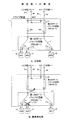
図8及び図9を用いて説明すると。図8,図9は二重化されたFC−ALの負荷分散を実現する方法を示す図(その1),(その2)である。図8のA.にコントローラ・エンクロージャ(CE)にドライブエンクロージャ(DE)が♯1〜♯3で示すように3台接続され,各ドライブ・エンクロージャ(DE)は,4個のハードディスク(HDD)が配置され,各DE♯1〜♯3の各ハードディスクは,1系のPBC♯1−1,PBC♯2−1,PBC♯3−1を介する1系のFC−AL♯1によりアクセスできると共に,2系のPBC♯1−2,PBC♯2−2,PBC♯3−2を介する2系のFC−AL♯2によりアクセスできる。このようなRAID装置は,正常時にはA.に示すように二重化されたFC−AL(♯1,♯2)のインタフェースで各ドライブ・エンクロージャ(DE)♯1〜♯3と通信を行い,各FC−ALはそれぞれ6台ずつのハードディスクと通信している。この状態において図のB.に示すようにPBC♯2−1のPBC素子が故障すると,PBC♯2−1経由で通信していたハードディスクはPBC♯2−2経由に切り替える。この状態では,2つのFC−AL(♯1,♯2)からの通信対象がFC−AL♯1経由が4台でFC−AL♯2経由が8台になり,片側への偏りが生じる。ここで,図9に示すように通信経路を切り替える。すなわち,FC−AL♯1側が6台,FC−AL♯2側が6台となる負荷分散を維持することが可能となる。
This will be described with reference to FIGS. 8 and 9. FIG. 8 and FIG. 9 are diagrams (No. 1) and (No. 2) showing a method of realizing load sharing of the duplicated FC-AL. A. of FIG. As shown by # 1 to # 3, three drive enclosures (DE) are connected to the controller enclosure (CE), and each drive enclosure (DE) has four hard disks (HDDs) arranged therein. The
図10は実施例3において第2のポートバイパス回路40のPBC素子が故障した場合の切替えの状態である。この場合,第2のポートバイパス回路40のPBC素子が故障したことにより,現用系のFC−ALのループを使用することができないので,現用系のケーブル2a〜2dを介するループを閉鎖して,予備系のループに接続された第3のポートバイパス回路41を,ハードディスク12に接続する第1のポートバイパス回路42と接続するよう切替スイッチを切替える。すなわち,第1のポートバイパス回路42内のPBC素子(または切替スイッチ)42aをバイパス状態とし,PBC素子の切替スイッチ42bを第3のポートバイパス回路41の切替スイッチ41dと接続するよう切替スイッチを切替える。これにより,予備系のケーブル2e〜2h及び第3のポートバイパス回路41,第1のポートバイパス回路42を通るループが形成され,図示省略されたコントローラエンクロージャと通信することができる。
FIG. 10 shows a switching state when the PBC element of the second
この場合,ケーブルの二重化同様,FC−ALトポロジが崩れないよう,正常時は不要な接続をPBC素子でバイパスし,異常発生時に異常個所を切り離し,代替個所のバイパスを解除する。 In this case, as in the case of cable duplication, in order to prevent the FC-AL topology from collapsing, unnecessary connections are bypassed with PBC elements in the normal state, abnormal portions are disconnected when an abnormality occurs, and the alternate portion bypass is released.
上記した図10の例は,第2のポートバイパス回路40のPBC素子が故障した場合であるが,第3のポートバイパス回路41のPBC素子が故障した場合に,第2のポートバイパス回路40が正常な状態になっている場合は,第3のポートバイパス回路41を切り離し,第2のポートバイパス回路40を第1のポートバイパス回路に接続し,FC−ALのループも予備系のケーブル2e〜2hから現用系のケーブル2a〜2dへ切り替えることで,通信を維持することができる。
The example of FIG. 10 described above is a case where the PBC element of the second
上記したFC−ALのループの障害発生時のハードディスク等のデバイス故障特定方法は,上記特許文献2に記載された手法がある。この手法は,デバイス故障の特定方法であり,本発明が対象としてる故障部品には該当しないが,デバイス故障でないことを確認するため,最初にこのような手法により切り分ける。その後,図11に示すフローによりPBC素子,ケーブルの障害個所を特定することができる。
As a method for identifying a failure of a device such as a hard disk when a failure of the FC-AL loop occurs, there is a method described in
図11は故障個所の切り分けのフローチャートである。このフローチャートは,上記図6〜図10に示す実施例3の構成に示す構成(第1〜第3のポートバイパス回路40〜42)を備えたドライブ装置における障害の特定を行う例に適用することができる。
FIG. 11 is a flowchart for identifying a fault location. This flowchart is applied to an example in which a failure is identified in a drive device having the configuration (first to third
最初にループ障害が発生すると,ハードディスク(HDD)のバイパス(各ハードディスクに対応して一つずつ形成)による障害を特定し(図11のS1),ハードディスクのバイパスで障害が回復したかを判別し(同S2),障害が回復した場合はハードディスクが障害の要因であると判定し(同S3),障害特定を終了する。ステップS2でループ障害が回復しない場合,第2のポートバイパス回路40のPBC素子のバイパス(図6の第2のポートバイパス回路40のPBC40d)を形成し(同S4),ループ障害が回復したか判別する(同S5)。ここでループ障害が回復したことが判別されると,第1のポートバイパス回路のPBC素子(図6のPBC42c〜42nの何れか)が障害の要因であると判定し(図11のS6),ステップS5で障害が回復しない場合は,第2のポートバイパス回路のバイパスを解除し(同S7),ケーブルの予備系への切替え(図6の第3のポートバイパス回路41のPBC41dを切替えて接続状態とし,ケーブル2e〜2hの予備系を介するループを形成)を行う(図11のS8)。
When a loop failure occurs for the first time, the failure caused by the hard disk (HDD) bypass (one corresponding to each hard disk is formed) is identified (S1 in FIG. 11), and it is determined whether the failure has been recovered by the hard disk bypass. (S2), if the failure is recovered, it is determined that the hard disk is the cause of the failure (S3), and the failure identification is terminated. If the loop failure is not recovered in step S2, a bypass of the PBC element of the second port bypass circuit 40 (
続いてループ障害が回復したか判別し(図11のS9),回復しない場合は障害要因なしとして,他のデバイスの診断へ移行し,回復した場合は第1のポートバイパス回路42をループに接続する(同S10)。この場合,図6の第1のポートバイパス回路42のPBC42bを切替えて第3のポートバイパス回路41のPBC41dと接続してループを形成する。この状態で,ループ障害(通信ができない等の状態)が再現したか判別し(図11のS11),障害が再現した場合は第1のポートバイパス回路42のPBC素子が障害の要因であると判定し(同S12),障害特定を終了する。ステップS11において,ループ障害が再現しない場合は,現用系のループを形成するケーブルが障害の要因であると判定し(同S13),障害特定を終了する。
Subsequently, it is determined whether or not the loop fault has been recovered (S9 in FIG. 11). If it does not recover, it is determined that there is no fault factor, and the process proceeds to diagnosis of another device. If the fault has recovered, the first
なお,PBC素子の受信端にファイバチャネル(FC)信号の品質を観測する機能を持つものが使用されており,このような素子を用いる場合は,上記図11に示すような切り分け手順を実施する必要はない。ファイバチャネルループがトポロジとして一つの円構造であるため,障害発生時は,その場所からコマンドの送受信元であるコントローラエンクロージャでバイパスまでの各観測点で異常を検出する。この場合,最初に異常を検出したポイントが障害個所となり,その障害個所に対応して,上記実施例1乃至実施例3の構成による切替え制御を実行する。 In addition, what has the function which observes the quality of a fiber channel (FC) signal is used for the receiving end of a PBC element, and when using such an element, the isolation | separation procedure as shown in said FIG. 11 is implemented. There is no need. Since the Fiber Channel loop has a single topology as a topology, when a failure occurs, an abnormality is detected at each observation point from the location to the bypass in the controller enclosure that is the command transmission / reception source. In this case, the point where the abnormality is first detected becomes a failure location, and the switching control according to the configuration of the first to third embodiments is executed corresponding to the failure location.
1 ドライブ装置(♯2)
10 第2のポートバイパス回路(PBC♯2−2)
11 第1のポートバイパス回路(PBC♯2−1)
12 複数のハードディスク(HDD)
2a,2b 上流側に接続するループのケーブル
2c,2d 下流側に接続するループのケーブル
1 Drive device (# 2)
10 Second port bypass circuit (PBC # 2-2)
11 First port bypass circuit (PBC # 2-1)
12 Multiple hard disks (HDD)
2a, 2b Loop cable connected to the
Claims (3)
前記ドライブ装置の前記各デバイスのそれぞれに設けたポートバイパス素子を直列に接続することにより形成されたループを含むポートバイパス回路を備え,
前記ポートバイパス回路のループ上に現用系のループを形成する上流側へのケーブルと下流側へのケーブルのそれぞれを前記ポートバイパス回路のループに直列に接続するか,バイパスするかを切り替える該各ケーブルに対応する現用系の2つのポートバイパス素子と,予備系のループを形成する上流側へのケーブルと下流側へのケーブルのそれぞれを前記ポートバイパス回路のループに直列に接続するかバイパスするかを切り替える該各ケーブルに対応する予備系の2つのポートバイパス素子とを直列に設け,
通常は前記現用系の上流側と下流側のケーブルを前記ポートバイパス回路と直列に接続して前記予備系の各ケーブルをバイパス接続し,前記現用系のループに障害が検出されると,前記現用系の上流側と下流側のポートバイパス素子をバイパスし,前記予備系の上流側と下流側のポートバイパス素子を前記ポートバイパス回路のループに直列に接続するよう切替えることを特徴とするドライブ装置をFC−ALにより接続した情報処理システム。 In an information processing system in which drive devices having a plurality of devices are sequentially connected by FC-AL,
A port bypass circuit including a loop formed by connecting a port bypass element provided in each of the devices of the drive device in series;
Each cable for switching whether the upstream cable and the downstream cable forming a working loop on the loop of the port bypass circuit are connected in series to the loop of the port bypass circuit or bypassed. Whether to connect each of the two upstream port bypass elements corresponding to the above and the upstream cable forming the standby loop and the downstream cable to the port bypass circuit loop in series or bypass. Two port bypass elements in the standby system corresponding to each cable to be switched are provided in series,
Normally, the upstream and downstream cables of the working system are connected in series with the port bypass circuit, and the backup system cables are bypassed. When a fault is detected in the working loop, the working system A drive device characterized in that the upstream and downstream port bypass elements of the system are bypassed, and the upstream and downstream port bypass elements of the standby system are switched to be connected in series to the loop of the port bypass circuit. Information processing system connected by FC-AL.
前記ドライブ装置は,各デバイスに対応する各ポートバイパス素子を順次接続した第1のポートバイパス回路と,前記第1のポートバイパス回路の上位に設けられ前記第1のポートバイパス回路の両端の端子と接続されたポートバイパス素子を備えた第2のポートバイパス回路を備え,
前記第2のポートバイパス回路は,前記第1のポートバイパス回路の両端子をそれぞれFC−ALのループを形成する上流側のケーブルと下流側のケーブルとに接続するか,前記両端子間をバイパスするかの切り替え可能なポートバイパス素子を備え,
前記第1のポートバイパス回路の上位に設けられ前記第1のポートバイパス回路のループ上に直列に接続されたポートバイパス素子を介して予備系のループを形成する上流側のケーブルと下流側のケーブルとに接続された第3のポートバイパス回路を設けたことを特徴とするドライブ装置をFC−ALにより接続した情報処理システム。 In an information processing system in which drive devices with multiple devices are connected by FC-AL,
The drive device includes a first port bypass circuit in which port bypass elements corresponding to devices are sequentially connected, terminals provided at both ends of the first port bypass circuit, which are provided above the first port bypass circuit. A second port bypass circuit having a connected port bypass element;
The second port bypass circuit connects both terminals of the first port bypass circuit to an upstream cable and a downstream cable forming a FC-AL loop, respectively, or bypasses the two terminals. With a switchable port bypass element
An upstream cable and a downstream cable that form a standby loop via a port bypass element that is provided above the first port bypass circuit and connected in series on the loop of the first port bypass circuit And a third port bypass circuit connected to each other, and an information processing system in which drive devices are connected by FC-AL.
前記第1のポートバイパス回路のループ上の前記第3のポートバイパス回路に接続するポートバイパス素子は,前記第2のポートバイパス回路が正常な状態ではバイパスされ,前記第2のポートバイパス回路のポートバイパス素子に障害が発生すると,前記第1のポートバイパス回路のループ上の前記第2のポートバイパス回路に接続するポートバイパス素子をバイパスし,前記第3のポートバイパス回路に接続するポートバイパス素子を前記予備系のケーブルを介するループを形成するよう切り替えられることを特徴とするドライブ装置をFC−ALにより接続した情報処理システム。 In claim 2,
The port bypass element connected to the third port bypass circuit on the loop of the first port bypass circuit is bypassed when the second port bypass circuit is normal, and the port of the second port bypass circuit When a failure occurs in the bypass element, the port bypass element connected to the second port bypass circuit on the loop of the first port bypass circuit is bypassed, and the port bypass element connected to the third port bypass circuit is An information processing system in which drive devices that are switched to form a loop through the backup cable are connected by FC-AL.
Priority Applications (1)
| Application Number | Priority Date | Filing Date | Title |
|---|---|---|---|
| JP2006332796A JP5082418B2 (en) | 2006-12-11 | 2006-12-11 | Information processing system with drive devices connected by FC-AL |
Applications Claiming Priority (1)
| Application Number | Priority Date | Filing Date | Title |
|---|---|---|---|
| JP2006332796A JP5082418B2 (en) | 2006-12-11 | 2006-12-11 | Information processing system with drive devices connected by FC-AL |
Publications (2)
| Publication Number | Publication Date |
|---|---|
| JP2008146354A JP2008146354A (en) | 2008-06-26 |
| JP5082418B2 true JP5082418B2 (en) | 2012-11-28 |
Family
ID=39606468
Family Applications (1)
| Application Number | Title | Priority Date | Filing Date |
|---|---|---|---|
| JP2006332796A Expired - Fee Related JP5082418B2 (en) | 2006-12-11 | 2006-12-11 | Information processing system with drive devices connected by FC-AL |
Country Status (1)
| Country | Link |
|---|---|
| JP (1) | JP5082418B2 (en) |
Family Cites Families (5)
| Publication number | Priority date | Publication date | Assignee | Title |
|---|---|---|---|---|
| JP2000298555A (en) * | 1999-04-13 | 2000-10-24 | Hitachi Ltd | Loop type array controller and loop connection storage device |
| JP4317436B2 (en) * | 2003-12-16 | 2009-08-19 | 株式会社日立製作所 | Disk array system and interface conversion device |
| JP2005339216A (en) * | 2004-05-27 | 2005-12-08 | Hitachi Ltd | Memory control system |
| JP4669263B2 (en) * | 2004-11-04 | 2011-04-13 | 株式会社日立製作所 | Storage device |
| JP4635941B2 (en) * | 2006-03-31 | 2011-02-23 | 日本電気株式会社 | Disk array subsystem |
-
2006
- 2006-12-11 JP JP2006332796A patent/JP5082418B2/en not_active Expired - Fee Related
Also Published As
| Publication number | Publication date |
|---|---|
| JP2008146354A (en) | 2008-06-26 |
Similar Documents
| Publication | Publication Date | Title |
|---|---|---|
| US6055228A (en) | Methods and apparatus for dynamic topology configuration in a daisy-chained communication environment | |
| US5991891A (en) | Method and apparatus for providing loop coherency | |
| KR100831639B1 (en) | Information processing apparatus, communication load decentralizing method, and communication system | |
| US8402212B2 (en) | Storage system and management method of its storage medium | |
| US20080215910A1 (en) | High-Availability Networking with Intelligent Failover | |
| JP2001222385A (en) | Storage device and information processing system | |
| JP2010506332A (en) | System and method for connection of a SAS RAID controller device channel between redundant storage subsystems | |
| JP3740969B2 (en) | Optical cross-connect device | |
| US7263060B1 (en) | Multiple switch protected architecture | |
| KR100340686B1 (en) | The Apparatus for Redundant Interconnection between Multiple Hosts and RAID | |
| JP2001256203A (en) | Redundant crossbar switch system | |
| US7861123B1 (en) | Managing loop interface failure | |
| JP2007272702A (en) | Disk array subsystem, and redundancy maintenance method and program | |
| US7568119B2 (en) | Storage control device and storage control device path switching method | |
| JP2016100843A (en) | Relay device | |
| US8255737B1 (en) | System and method for a redundant communication fabric in a network storage system | |
| WO2003091887A1 (en) | Method and apparatus for dual porting a single port serial ata disk drive | |
| JP5082418B2 (en) | Information processing system with drive devices connected by FC-AL | |
| JP2006285519A (en) | Failure diagnosis method for data transfer system, data transfer system, and data storage device | |
| JP4024607B2 (en) | Optical cross-connect device | |
| US6980510B1 (en) | Host interface adaptive hub storage system | |
| JP4395766B2 (en) | Fault analysis system, method and program | |
| WO2014030732A1 (en) | Communication system, communication device, protection switching method, and switching program | |
| US20180241820A1 (en) | Software-defined storage apparatus, and system and storage method thereof | |
| JP3621634B2 (en) | Redundant configuration switching system |
Legal Events
| Date | Code | Title | Description |
|---|---|---|---|
| A621 | Written request for application examination |
Free format text: JAPANESE INTERMEDIATE CODE: A621 Effective date: 20090810 |
|
| A131 | Notification of reasons for refusal |
Free format text: JAPANESE INTERMEDIATE CODE: A131 Effective date: 20120124 |
|
| A977 | Report on retrieval |
Free format text: JAPANESE INTERMEDIATE CODE: A971007 Effective date: 20120125 |
|
| A521 | Written amendment |
Free format text: JAPANESE INTERMEDIATE CODE: A523 Effective date: 20120326 |
|
| RD03 | Notification of appointment of power of attorney |
Free format text: JAPANESE INTERMEDIATE CODE: A7423 Effective date: 20120326 |
|
| RD04 | Notification of resignation of power of attorney |
Free format text: JAPANESE INTERMEDIATE CODE: A7424 Effective date: 20120326 |
|
| TRDD | Decision of grant or rejection written | ||
| A01 | Written decision to grant a patent or to grant a registration (utility model) |
Free format text: JAPANESE INTERMEDIATE CODE: A01 Effective date: 20120807 |
|
| A01 | Written decision to grant a patent or to grant a registration (utility model) |
Free format text: JAPANESE INTERMEDIATE CODE: A01 |
|
| A61 | First payment of annual fees (during grant procedure) |
Free format text: JAPANESE INTERMEDIATE CODE: A61 Effective date: 20120820 |
|
| R150 | Certificate of patent or registration of utility model |
Ref document number: 5082418 Country of ref document: JP Free format text: JAPANESE INTERMEDIATE CODE: R150 Free format text: JAPANESE INTERMEDIATE CODE: R150 |
|
| FPAY | Renewal fee payment (event date is renewal date of database) |
Free format text: PAYMENT UNTIL: 20150914 Year of fee payment: 3 |
|
| LAPS | Cancellation because of no payment of annual fees |