JP5075890B2 - Semiconductor device and manufacturing method of semiconductor device - Google Patents
Semiconductor device and manufacturing method of semiconductor device Download PDFInfo
- Publication number
- JP5075890B2 JP5075890B2 JP2009201415A JP2009201415A JP5075890B2 JP 5075890 B2 JP5075890 B2 JP 5075890B2 JP 2009201415 A JP2009201415 A JP 2009201415A JP 2009201415 A JP2009201415 A JP 2009201415A JP 5075890 B2 JP5075890 B2 JP 5075890B2
- Authority
- JP
- Japan
- Prior art keywords
- electrode
- resist
- wafer
- sealing material
- seed layer
- Prior art date
- Legal status (The legal status is an assumption and is not a legal conclusion. Google has not performed a legal analysis and makes no representation as to the accuracy of the status listed.)
- Expired - Fee Related
Links
Images


Classifications
-
- H10W72/0198—
-
- H10W72/019—
-
- H10W74/014—
-
- H10W74/019—
-
- H10W74/111—
-
- H10W46/00—
-
- H10W46/401—
-
- H10W46/607—
-
- H10W72/01331—
-
- H10W72/59—
-
- H10W74/00—
Landscapes
- Internal Circuitry In Semiconductor Integrated Circuit Devices (AREA)
- Encapsulation Of And Coatings For Semiconductor Or Solid State Devices (AREA)
- Dicing (AREA)
Abstract
Description
本発明は、半導体チップを組み込んだ半導体装置及び半導体装置の製造方法に関する。 The present invention relates to a semiconductor device incorporating a semiconductor chip and a method for manufacturing the semiconductor device.
従来半導体装置は、以下の特許文献1に示されるように半導体チップと外部電極との間の電気的接続をボンディングワイヤを使用して行っていた。例えば、ワイヤボンディングを使用した半導体装置を簡易に示す図25を用いて説明すると、半導体装置1000は、その表面と裏面の両面にそれぞれ表面側電極1001aと裏面側電極1001bとを有する半導体チップ1001を備えている。この半導体チップ1001は、その裏面側電極1001bと図示しない導電性部材を介して外部電極1002が接続されるとともに、半導体チップ1001の表面側電極1001aは外部電極1003との間をボンディングワイヤ1004によって接続されている。この半導体装置1000は、封止樹脂1005によって気密に封止されている。半導体装置1000は、基板1006に設けられた配線パッド1007と外部電極1002及び1003とが図示しない導電性部材を介して接続されることで電気的に接続されている。
Conventional semiconductor devices have used a bonding wire for electrical connection between a semiconductor chip and an external electrode, as shown in
また、その他の小型電子部品の形態としては、例えば、図26に示すような形態も挙げることができる。この半導体装置1010は、積層コンデンサ1011とその両端に接続された一対の外部電極1012,1012から構成されている。この外部電極1012,1012は積層コンデンサ1011と接続されている面を除く5つの面がそれぞれ電極となっている。そして基板1013上に設けられた配線パッド1014上に外部電極1012,1012が載置され、図26に示すように配線パッド1014から外部電極1012,1012にかけてはんだ1015が盛られ、これにより基板1013と半導体装置1010とは電気的に接続される。
Further, as another form of the small electronic component, for example, a form as shown in FIG. 26 can be cited. The
しかしながら、上述した特許文献1に開示された構成をもつボンディングワイヤを使用した半導体装置の場合、次のような問題点がある。
However, the semiconductor device using the bonding wire having the configuration disclosed in
すなわち、携帯電話等、電子機器の普及に伴って、例えば、電子部品の電気特性の向上等が求められているが、このボンディングワイヤを使用した半導体装置では、ボンディングワイヤの部分で電気抵抗値が増加してしまうため電気特性の向上を図ることは難しい。また、図25にも示されているように、半導体チップ1001の表面側電極1001aから外部電極1003への接続は1対1であり、個々に接続を行うことになるため製造工程の削減及び製造時間の短縮を図ることができず、結果として生産性の向上を図れない。
That is, with the widespread use of electronic devices such as mobile phones, for example, improvement in electrical characteristics of electronic components is required. However, in a semiconductor device using this bonding wire, the electrical resistance value is in the bonding wire portion. Therefore, it is difficult to improve the electrical characteristics. Also, as shown in FIG. 25, the connection from the front-
また、仮に図26に示すような積層コンデンサ内に半導体チップを封止した構造の場合、ボンディングワイヤを使用しない分ボンディングワイヤを使用した半導体装置1000に比べて電気特性の向上は図れるものの、半導体チップの封止時に内部の素子が壊れてしまうといった問題が生じうる。すなわち、図26に示す積層コンデンサ1011は、硬い絶縁物質層を積層して素子(導体)を挟み込み熱圧着を行って製造するが、半導体チップを実装する場合は、半導体チップにかかる負荷によって半導体チップに損傷を与える場合があり、製造の歩留まりが悪くなってしまう。半導体チップとその半導体チップを挟む部材との間で信頼性試験や落下による衝撃によって接着界面の剥離が生ずる可能性もあり、このことも製造の歩留まりを悪くする一因となり得る。
In addition, in the case of the structure in which the semiconductor chip is sealed in the multilayer capacitor as shown in FIG. 26, the electrical characteristics can be improved compared to the
さらに図26に示した半導体装置1010の製造方法の一例として次の方法が採用される場合がある。すなわち、まず一定の間隔(ストリート部)を設けて再配列した半導体チップを樹脂封止した後、この樹脂に半導体チップの表裏に形成された電極と外部電極1012とを接続するための孔をレーザー加工によって設け、めっき処理により外部電極1012を形成する。このレーザー加工工程では、レーザーから印加されるエネルギー(主に熱エネルギー)が半導体チップの表裏に形成された電極上に設けられている保護膜(例えば、ニッケル(Ni)/金(Au)等の金属膜)を除去してしまう可能性があり、電極にとって決して良い状態ではない。保護膜自体を厚くすることも考えられるが、余計な多くの材料を必要としてしまう。また、半導体チップに形成された電極の全てに対して個々に孔を設ける必要から、レーザー加工工程は多くの時間を必要とする。
Further, the following method may be employed as an example of the manufacturing method of the
また、半導体チップの片面を樹脂封止すると、樹脂封止の工程においては封止樹脂を加熱して硬化させた後に常温まで降温させる流れを経ることから、ワーク(ウェハ及び封止樹脂)に反りが生じてしまう可能性もある。 In addition, when one side of the semiconductor chip is resin-sealed, in the resin sealing process, the sealing resin is heated and cured, and then the temperature is lowered to room temperature, so that the workpiece (wafer and sealing resin) warps. May occur.
本発明は上記課題を解決するためになされたものであり、本発明の目的は、ボンディングワイヤを使用しない構造を備えることで電気特性を向上させつつ高い信頼性を確保し、レーザー加工工程をなくし製造時間の短縮を進めて生産性の向上を図ることの可能な半導体装置及び半導体装置の製造方法を提供することである。 The present invention has been made to solve the above-mentioned problems, and an object of the present invention is to provide a structure that does not use a bonding wire to ensure high reliability while eliminating the laser processing step while improving electrical characteristics. It is an object of the present invention to provide a semiconductor device and a semiconductor device manufacturing method capable of improving productivity by shortening the manufacturing time.
本発明の実施の形態に係る第1の特徴は、第1の表面に半導体素子の第1の電極が配設され、第1の表面と対向する第2の表面に半導体素子の第2の電極が配設された半導体チップと、第1の電極及び第2の電極の領域のみを露出させその他の半導体チップ表面を封止する封止材と、第1の電極または第2の電極と接続され、第1の表面または第2の表面からの厚みが封止材の厚みと同一である内部電極と、内部電極と接続されるとともに、封止材上にも形成された少なくとも半導体チップ幅よりも幅の広い外部電極と、外部電極の内部電極と接続される面を除く5つの面を覆うめっき膜とを備える半導体装置であって、第1の電極と内部電極との間、第2の電極と内部電極との間、内部電極と外部電極との間にはシード層が介在されていることにある。 According to the first feature of the embodiment of the present invention, the first electrode of the semiconductor element is disposed on the first surface, and the second electrode of the semiconductor element is disposed on the second surface opposite to the first surface. Are connected to the first electrode or the second electrode, the semiconductor chip on which the first electrode and the second electrode are exposed, the sealing material that exposes only the first electrode region and the second electrode region, and the other semiconductor chip surface is sealed. The internal electrode whose thickness from the first surface or the second surface is the same as the thickness of the encapsulant, and connected to the internal electrode and at least larger than the width of the semiconductor chip formed on the encapsulant A semiconductor device comprising a wide external electrode and a plating film covering five surfaces excluding a surface connected to the internal electrode of the external electrode, wherein the second electrode is provided between the first electrode and the internal electrode. between the internal electrodes, a seed layer between the inner electrode and the outer electrode is interposed between In the door.
本発明の実施の形態に係る第2の特徴は、半導体装置の製造方法において、素子電極を形成したウェハ(以下、単にウェハ)の一方の面に第1のシード層を形成する工程と、ウェハの一方の面に第1のレジストを貼付する工程と、第1のレジスト上にウェハの一方の面に形成された第1の電極が露出する位置に開口部が設けられるように位置合わせされるマスクを搭載する工程と、マスク外から第1のレジストに向けて露光し、さらに現像を行うことで、第1のレジストに第1の孔を形成する工程と、第1のレジスト上からめっき処理を行い、第1の孔にめっきを充填し第1の内部電極を形成する第1のめっき処理工程と、ウェハから第1のレジストを剥離する工程と、ウェハから第1のシード層をエッチングにより除去する工程と、ウェハ上の隣接する第1の内部電極間をダイサーによって所定の位置まで切断する工程と、ダイサーによって切断され形成された溝を充填し、第1の内部電極上まで第1の封止材にて封止する工程と、第1の内部電極が露出するように第1の封止材を研削する工程と、ウェハの他方の面を所望の半導体チップの厚みとなるまで研削し、素子を形成したウェハを個々の半導体チップに分割する工程と、ウェハの研削されて現われた面に第2のシード層を形成する工程と、第2のシード層上に第2のレジストを貼付する工程と、第2のレジスト上にマスクを搭載する工程と、マスク外から第2のレジストに向けて露光し、さらに現像を行うことで、第2のレジストに第2の孔を形成する工程と、第2のレジスト上からめっき処理を行い、第2の孔にめっきを充填し第2の内部電極を形成する第2のめっき処理工程と、ウェハから第2のレジストを剥離する工程と、ウェハから第2のシード層をエッチングにより除去する工程と、第2の内部電極上を覆うように第2の封止材にて封止する工程と、第2の内部電極が露出するように第2の封止材を研削する工程と、第1の内部電極及び第1の封止材上に第3のシード層を形成する工程と、第3のシード層上に第3のレジストを貼付する工程と、第3のレジスト上にマスクを搭載する工程と、マスク外から第3のレジストに向けて露光し、さらに現像を行うことで、第3のレジストに第3の孔を形成する工程と、第3のレジスト上からめっき処理を行い、第3の孔にめっきを充填し第1の外部電極を形成する第3のめっき処理工程と、第2の内部電極及び第2の封止材上に第4のシード層を形成する工程と、第4のシード層上に第4のレジストを貼付する工程と、第4のレジスト上にマスクを搭載する工程と、マスク外から第4のレジストに向けて露光し、さらに現像を行うことで、第4のレジストに第4の孔を形成する工程と、第4のレジスト上からめっき処理を行い、第4の孔にめっきを充填し第2の外部電極を形成する第4のめっき処理工程と、第1の封止材及び第2の封止材から第3のレジスト及び第4のレジストを剥離する工程と、第3のシード層及び第4のシード層をエッチングにより除去する工程と、隣接する第1の外部電極及び第2の外部電極の間をダイサーによって切断して個々の半導体装置へと個片化する工程と、個片化された半導体装置の第1の外部電極の5面及び第2の外部電極の5面に対してめっき処理を行う第5のめっき処理工程とを備える。 A second feature according to the embodiment of the present invention is that, in the method of manufacturing a semiconductor device, a step of forming a first seed layer on one surface of a wafer (hereinafter simply referred to as a wafer) on which an element electrode is formed, and the wafer A step of attaching a first resist to one surface of the wafer, and alignment so that an opening is provided at a position where the first electrode formed on one surface of the wafer is exposed on the first resist. A step of mounting a mask, a step of forming a first hole in the first resist by performing exposure to the first resist from the outside of the mask and further developing, and a plating process from above the first resist A first plating process for filling the first hole with plating to form a first internal electrode, a step for removing the first resist from the wafer, and etching the first seed layer from the wafer. Removal process and wafer A step of cutting between adjacent first internal electrodes to a predetermined position with a dicer, filling a groove formed by cutting with a dicer, and sealing the first internal electrode with the first sealing material A step of grinding the first encapsulant so that the first internal electrode is exposed, and grinding the other surface of the wafer to a desired semiconductor chip thickness to form a wafer on which an element is formed. Dividing the semiconductor chips into individual semiconductor chips; forming a second seed layer on the ground surface of the wafer; attaching a second resist on the second seed layer; A step of mounting a mask on the resist, a step of forming a second hole in the second resist by performing exposure to the second resist from the outside of the mask and further developing, and a step on the second resist Plating process is performed on the second hole. A second plating process for forming a second internal electrode by filling the substrate, a step of removing the second resist from the wafer, a step of removing the second seed layer from the wafer by etching, and a second internal Sealing with a second sealing material so as to cover the electrode, grinding the second sealing material so that the second internal electrode is exposed, and the first internal electrode and the first Forming a third seed layer on the encapsulant, applying a third resist on the third seed layer, mounting a mask on the third resist, and from outside the mask By exposing to the third resist and further developing, a step of forming a third hole in the third resist, a plating process is performed on the third resist, and the third hole is plated. A third plating step for filling and forming a first external electrode; and a second internal electrode And a step of forming a fourth seed layer on the second sealing material, a step of attaching a fourth resist on the fourth seed layer, a step of mounting a mask on the fourth resist, The fourth resist is exposed to the fourth resist from the outside of the mask, and further developed to form a fourth hole in the fourth resist, and the fourth resist is subjected to a plating process, and the fourth hole is formed. A fourth plating treatment step of filling the plating and forming the second external electrode, a step of peeling the third resist and the fourth resist from the first sealing material and the second sealing material, The step of removing the third seed layer and the fourth seed layer by etching, and cutting between the adjacent first external electrode and second external electrode by a dicer to separate into individual semiconductor devices. A process, five surfaces of the first external electrode of the separated semiconductor device, and And a fifth plating treatment step of performing plating processing on the five surfaces of the second external electrode.
本発明の実施の形態に係る第3の特徴は、第1の表面に半導体素子の第1の電極が配設され、第1の表面と対向する第2の表面に半導体素子の第2の電極が配設された半導体チップと、第1の電極及び第2の表面の領域のみを露出させその他の半導体チップ表面を封止する封止材と、第1の電極と接続され、第1の表面からの厚みが封止材の厚みと同一である内部電極と、内部電極と接続されるとともに、封止材上にも形成され、少なくとも半導体チップ幅よりも幅の広い第1の外部電極と、第2の電極を含む第2の表面に接続されるとともに、封止材上にも形成され、少なくとも半導体チップ幅よりも幅の広い第2の外部電極と、第1の外部電極の内部電極と接続される面を除く5つの面を覆う第1の外装めっき膜と、第2の外部電極の第2の電極と接続される面を除く5つの面を覆う第2の外装めっき膜と、を備える半導体装置であって、前記第1の電極と前記内部電極との間、前記内部電極と前記第1の外部電極との間、前記第2の電極と前記第2の外部電極との間にはシード層が介在されていることにある。
According to a third feature of the embodiment of the present invention, the first electrode of the semiconductor element is disposed on the first surface, and the second electrode of the semiconductor element is disposed on the second surface opposite to the first surface. A semiconductor chip on which the first electrode and the second surface region are exposed, the other semiconductor chip surface is sealed, and the first surface is connected to the first electrode. An internal electrode having a thickness equal to the thickness of the encapsulant, and a first external electrode connected to the internal electrode and also formed on the encapsulant and having a width that is at least wider than the width of the semiconductor chip; A second external electrode connected to the second surface including the second electrode and also formed on the encapsulant and having a width wider than at least the semiconductor chip width; and an internal electrode of the first external electrode; A first outer plating film covering five surfaces excluding the surfaces to be connected, and a second outer electrode first A second exterior plating film that covers five surfaces excluding the surface connected to the electrode of the first electrode, between the first electrode and the internal electrode, and between the internal electrode and the first electrode A seed layer is interposed between the second external electrode and the second external electrode.
本発明の実施の形態に係る第4の特徴は、半導体装置の製造方法において、素子電極を形成したウェハ(以下、単にウェハ)の一方の面に第1のシード層を形成する工程と、ウェハの一方の面に第1のレジストを貼付する工程と、第1のレジスト上にウェハの一方の面に形成された第1の電極が露出する位置に開口部が設けられるように位置合わせされるマスクを搭載する工程と、マスク外から第1のレジストに向けて露光し、さらに現像を行うことで、第1のレジストに第1の孔を形成する工程と、第1のレジスト上からめっき処理を行い、第1の孔にめっきを充填し第1の内部電極を形成する第1のめっき処理工程と、ウェハから第1のレジストを剥離する工程と、ウェハから第1のシード層をエッチングにより除去する工程と、ウェハ上の隣接する内部電極間をダイサーによって所定の位置まで切断する工程と、ダイサーによって切断され形成された溝を充填し、内部電極上まで封止材にて封止する工程と、内部電極が露出するように前記封止材を研削する工程と、ウェハの他方の面を所望の半導体チップの厚みとなるまで研削し、素子を形成したウェハを個々の半導体チップに分割する工程と、内部電極および封止材上に第2のシード層を形成する工程と、第2のシード層上に第2のレジストを貼付する工程と、第2のレジスト上に、内部電極が露出し、その中心が一致するような開口部が設けられるように位置合わせされるマスクを搭載する工程と、マスク外から第2のレジストに向けて露光し、さらに現像を行うことで、第2のレジストに第2の孔を形成する工程と、第2のレジスト上からめっき処理を行い、第2の孔にめっきを充填し第1の外部電極を形成する第2のめっき処理工程と、第2の電極および封止材上に第3のシード層を形成する工程と、第3のシード層上に第3のレジストを貼付する工程と、第3のレジスト上に、第2の電極が露出し、その中心が一致するような開口部が設けられるように位置合わせされるマスクを搭載する工程と、マスク外から第3のレジストに向けて露光し、さらに現像を行うことで、第3のレジストに第3の孔を形成する工程と、第3のレジスト上からめっき処理を行い、第3の孔にめっきを充填し第2の外部電極を形成する第3のめっき処理工程と、封止材から第2のレジスト及び第3のレジストを剥離する工程と、第2のシード層及び第3のシード層をエッチングにより除去する工程と、隣接する第1の外部電極及び第2の外部電極の間をダイサーによって切断して個々の半導体装置へと個片化する工程と、個片化された半導体装置の第1の外部電極の5面及び第2の外部電極の5面に対してめっき処理を行う第4のめっき処理工程とを備える。 According to a fourth aspect of the present invention, in the method for manufacturing a semiconductor device, a step of forming a first seed layer on one surface of a wafer (hereinafter simply referred to as a wafer) on which an element electrode is formed, and the wafer A step of attaching a first resist to one surface of the wafer, and alignment so that an opening is provided at a position where the first electrode formed on one surface of the wafer is exposed on the first resist. A step of mounting a mask, a step of forming a first hole in the first resist by performing exposure to the first resist from the outside of the mask and further developing, and a plating process from above the first resist A first plating process for filling the first hole with plating to form a first internal electrode, a step for removing the first resist from the wafer, and etching the first seed layer from the wafer. Removal process and wafer A step of cutting between adjacent internal electrodes to a predetermined position by a dicer, a step of filling a groove formed by cutting with a dicer and sealing with a sealing material on the internal electrode, and the internal electrode exposed Grinding the sealing material, grinding the other surface of the wafer to a desired semiconductor chip thickness, dividing the wafer on which the elements are formed into individual semiconductor chips, internal electrodes and sealing The step of forming the second seed layer on the stopper, the step of applying the second resist on the second seed layer, and the internal electrodes are exposed on the second resist, and the centers thereof coincide. A step of mounting a mask that is aligned so as to provide such an opening, and exposure to the second resist from the outside of the mask, followed by development, so that the second hole is formed in the second resist. Forming, and A second plating process for plating the second resist to fill the second hole and forming the first external electrode; and a third seed layer on the second electrode and the sealing material , Forming a third resist on the third seed layer, and providing an opening on the third resist so that the second electrode is exposed and its center coincides. A step of mounting a mask to be aligned in this way, a step of exposing the third resist from the outside of the mask, and further developing to form a third hole in the third resist; A plating process is performed from above the resist, a third plating process for filling the third hole with a plating to form a second external electrode, and peeling the second resist and the third resist from the sealing material Etching the second seed layer and the third seed layer Removing the first external electrode and the second external electrode adjacent to each other by cutting with a dicer into individual semiconductor devices, and the first semiconductor device separated into pieces. A fourth plating process for plating the five surfaces of the external electrode and the five surfaces of the second external electrode.
本発明によれば、ボンディングワイヤを使用しない構造を備えることで電気特性を向上させつつ高い信頼性を確保し、レーザー加工工程をなくし製造時間の短縮を進めて生産性の向上を図ることの可能な半導体装置及び半導体装置の製造方法を提供することができる。 According to the present invention, by providing a structure that does not use a bonding wire, it is possible to improve the electrical characteristics while ensuring high reliability, eliminate the laser processing step, reduce the manufacturing time, and improve productivity. A semiconductor device and a method for manufacturing the semiconductor device can be provided.
以下、本発明の実施の形態について図面を参照して詳細に説明する。 Hereinafter, embodiments of the present invention will be described in detail with reference to the drawings.
(第1の実施の形態)
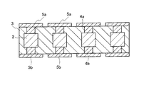
本発明の第1の実施の形態に係る半導体装置1の全体は、図1に示すような略直方体の形状をしている。半導体装置1には一対の外部電極5,5が設けられている。半導体装置1にはこれら一対の外部電極5,5に挟まれるように封止材3によって封止されている領域が設けられている。この封止材3は、半導体装置1の内部に設けられている半導体チップ2(図1では図示せず)を封止している。一対の外部電極5,5にはそれぞれめっき処理が施され、外部電極5が封止材3と接する面以外の5面が(外装)めっき膜6に覆われ、5面電極を形成している(図1では(外装)めっき膜6を表わしていない)。
(First embodiment)
The
後述するように、封止材3の色は任意に変更可能であり、半導体チップ2を封止するにあたって色の異なる少なくとも2色以上の封止材3を用いることで、半導体装置1の極性を表示させることも可能となる。なお、この半導体装置1は、上述した図26に示すような態様で用いられる。
As will be described later, the color of the sealing
図2は、図1に示す半導体装置1をA−A線で切断した状態を示す断面図である。半導体チップ2は、略立方体形状をしており、後述する電極が配設される2つの面を除く4面が半導体装置1の長手方向と平行となるように配置されている。半導体チップ2は、第1の表面2aに半導体素子の第1の電極2a1が配設され、第1の表面2aと対向する第2の表面2bに半導体素子の第2の電極2b1が配設されている。なお、ここでは説明の便宜上、「第1の表面2a」、「第2の表面2b」を特定し、それぞれに配設される電極を「第1の電極2a1」、「第2の電極2b1」と表わしているが、いずれを「第1」、「第2」と表わしても構わない。
FIG. 2 is a cross-sectional view showing a state in which the
図2に示すように、半導体チップ2は、その第1の電極2a1、第2の電極2b1が配設された領域を除いてその全体を封止材3によって封止されている。第1の電極2a1、第2の電極2b1が配設された領域は、第1の表面2a、第2の表面2bに対して垂直方向に孔が形成されており、その孔にはめっき処理によってめっきが充填され第1の内部電極4a又は第2の内部電極4bが形成されている。そして、この半導体チップ2の第1の表面2aには第1の内部電極4aが接続され、第2の表面2bには第2の内部電極4bが接続される。
As shown in FIG. 2, the
第1の内部電極4a、第2の内部電極4b及びこれら第1の内部電極4a、第2の内部電極4bの周囲を封止する封止材3上には、それぞれ第1の外部電極5a、第2の外部電極5bが形成されている。第1の内部電極4aには第1の外部電極5aが、第2の内部電極4bには第2の外部電極5bが接続される。この第1の外部電極5a、第2の外部電極5bがめっき処理されることによって(外装)めっき膜6a,6bに覆われ、上述したように5面電極を形成する。
On the sealing
その結果、図2に示されているように半導体チップ2は、半導体装置1の長手方向略中央に位置し封止材3によって挟まれる(封止される)とともに、第1の電極2a1,第2の電極2b1に接続されている第1の内部電極4a,第2の内部電極4bによって挟まれている。これら第1の内部電極4a、第2の内部電極4bはまた、第1の外部電極5a、第2の外部電極5bに挟まれている。
As a result, as shown in FIG. 2, the
第1の内部電極4a、第2の内部電極4bを封止する封止材3は、内部電極4(以下、第1の内部電極4a、第2の内部電極4bとをまとめて適宜「内部電極4」と表わす)と封止材3の接触面が図2の断面図に示されているように第1の表面2a、第2の表面2bに垂直方向に形成されている。
The sealing
但し、この面は、例えば第1の表面2a、第2の表面2bから外部電極5に向けてテーパが掛けられた形状とされる等、どのような形状に形成されていても構わない。また、この内部電極4が形成されている孔の大きさ、すなわち、内部電極4の大きさは半導体装置1の性能に合わせて任意に設定することができる。
However, this surface may be formed in any shape such as, for example, a shape that is tapered from the
次に、本発明の第1の実施の形態にかかる半導体装置1の製造方法について、適宜ワークの断面図である図3ないし図15を用いて説明する。
Next, a method for manufacturing the
まず、半導体素子(素子電極)が形成されたウェハWを用意する。図3にも示す通り、本発明の実施の形態に係る半導体装置の製造方法においては、厚いウェハWを用いる。このようなウェハWを使用することでその片面に封止材3を用いて封止したとしても反りが発生する可能性を低く抑えることができる。その厚さは任意に定めることができるが、以下述べる半導体装置の製造方法では、例えば、625μmの厚さが好適に用いられる。なお、以下、説明に際して適宜寸法を示すが、この示された寸法はあくまでも例として挙げた数値である。従って、本発明の実施の形態に係る半導体装置の大きさがこの数値に限定されるものではなく、製造工程においては要求される仕様に応じて任意にその数値を変更することが可能である。
First, a wafer W on which a semiconductor element (element electrode) is formed is prepared. As shown in FIG. 3, a thick wafer W is used in the method for manufacturing a semiconductor device according to the embodiment of the present invention. By using such a wafer W, even if it is sealed on one side using the sealing
このウェハWの一方の面(第1の表面2a)に、例えばチタン(Ti)、銅(Cu)からなる第1のシード層S1を形成する。図3に示すワークはこの第1のシード層S1が形成された状態を示すものである。このシード層Sはめっき処理を行う際に導通層となる層である。従って、以下に示される各シード層Sの形成に当たってはスパッタ、蒸着、無電解めっき等、その成膜手段は問わないが、十分な膜厚が必要とされる。また、シード層Sの材質は特に限定されず、例えば、後に形成される内部電極等の材質に合わせて任意に選定することが可能である。
A first seed layer S1 made of, for example, titanium (Ti) or copper (Cu) is formed on one surface (
なお、本発明の実施の形態においては、この状態でワークを予め熱する工程(プリヒート)を含む。この工程は、ワーク、特にシード層中の水分を揮発させる目的や、この後にシード層S上に貼付するレジストとの密着力を向上させるために行われる。但し、この工程は必須ではない。 In addition, in embodiment of this invention, the process (preheating) of preheating a workpiece | work in this state is included. This step is performed for the purpose of volatilizing the moisture in the workpiece, particularly the seed layer, and for improving the adhesion with the resist to be subsequently applied to the seed layer S. However, this step is not essential.
次に、図4に示すように、ウェハWの一方の面に成膜された第1のシード層S1上に第1のレジストR1を貼付する。この第1のレジストR1は内部電極4の形成に際して利用されることから、内部電極4の厚さとの関係でフィルム状のDFR(ドライフィルムレジスト:Dry Firm Resist)や液状のレジスト等を使用することができる。本発明の実施の形態ではDFRを使用している。 Next, as shown in FIG. 4, a first resist R <b> 1 is pasted on the first seed layer S <b> 1 formed on one surface of the wafer W. Since the first resist R1 is used when forming the internal electrode 4, a film-like DFR (Dry Firm Resist) or a liquid resist is used in relation to the thickness of the internal electrode 4. Can do. In the embodiment of the present invention, DFR is used.
この第1のレジストR1の上にマスクM1を搭載して露光する(図5参照)。このマスクM1には、予め露光時に用いるパターンが形成されている。このパターンは、露光、現像した際に第1の電極2a1を露出するべく、その位置に開口部が設けられるような位置に位置あわせが行われる。ここではガラスマスクを使用し、紫外線を照射して露光している。但し、マスクM1の材質や照射する光の性質は、第1のレジストR1の性質に合ったものを自由に選択することができる。 A mask M1 is mounted on the first resist R1 and exposed (see FIG. 5). On the mask M1, a pattern used at the time of exposure is formed in advance. This pattern is aligned at a position where an opening is provided at that position in order to expose the first electrode 2a1 when exposed and developed. Here, a glass mask is used, and exposure is performed by irradiating ultraviolet rays. However, the material of the mask M1 and the nature of the light to be irradiated can be freely selected according to the nature of the first resist R1.
その上で図6に示すように、DFRを現像してパターンを形成し、さらにDFRの残さ(スカム)の除去を行う(デスカム処理)。ここでのパターンは、内部電極4を形成するための孔(第1の孔11)であり、この工程を経ることによって、ウェハW上に格子状に第1の孔11が形成される。
Then, as shown in FIG. 6, the DFR is developed to form a pattern, and the DFR residue (scum) is removed (descum process). The pattern here is a hole (first hole 11) for forming the internal electrode 4, and the
図7は、上記説明した工程で形成された第1の孔11に、第1のレジストR1上からめっき処理を行う。この第1のめっき処理が行われることで、第1の孔11にめっきが充填され第1の内部電極4aが形成される。なお、この工程では電気めっきを施し、めっきとしては銅(Cu)を利用しているが、どのような金属をめっきとして使用しても構わない。従って、第1の内部電極4aは銅(Cu)でできている。
In FIG. 7, the
そして、シード層S1上に貼付した第1のレジストR1(DFR)を剥離する。併せて、第1のシード層S1もエッチングすることにより剥離する(図8参照)。この状態で、ウェハWに形成された第1の電極2a1上には第1の内部電極4aが形成されたことになる。
Then, the first resist R1 (DFR) attached on the seed layer S1 is peeled off. At the same time, the first seed layer S1 is also removed by etching (see FIG. 8). In this state, the first
さらに、図9に示すように隣接する第1の内部電極4a,4a間をダイサーで所定の位置まで切断してウェハW上に格子状の溝12を形成する。ここで「所定の位置」とは、任意に定めることができるが、この溝12には封止材3が充填され、半導体装置1の外形寸法に影響される。つまり、半導体チップ2の厚みはその電気的特性や半導体装置1の外形によって定められることから溝12の深さは最低限半導体チップ2の厚み分必要である。さらにこの後の製造工程を考慮すると、半導体チップ2の厚み以上の深さをもって溝12を形成する必要がある。例えば、本発明の実施の形態では、625μmの厚みを持つウェハWとして、溝12が250μmの深さとなるように形成している。
Further, as shown in FIG. 9, the adjacent first
次に、図10に示すように、溝12を充填するとともに第1の内部電極4aの上から第1の封止材3aを塗布してウェハWの一方の面を樹脂封止する。この第1の封止材3aは第1の内部電極4a上相当の厚みをもって塗布される。例えば、第1の内部電極4aの厚みを100μmとしたときに、第1の封止材3aの厚みはウェハWの表面から300μmである。
Next, as shown in FIG. 10, the
なお、ここでは第1の内部電極4aを封止する封止材を便宜的に「第1の封止材3a」としている。その上で、図11に示すように、第1の封止材3a及び第1の内部電極4aとが面一となるように研削し、第1の内部電極4aを第1の封止材3aから露出させる。この研削工程において第1の内部電極4aの厚みを調整することができる。
Here, the sealing material for sealing the first
そして、第1の封止材3aによって第1の内部電極4aが封止されたウェハWの一方の面ではなく、ウェハWの他方の面をグラインダを用いて薄くし、所望の半導体チップ2の厚みに合わせてその厚みを調整する(図12参照)。例えば、半導体チップ2の厚みは200μmであり、溝12の深さが250μmであるため、ここで素子を形成したウェハは、個々の半導体チップへと分割される。なお、グラインダを使用することによってウェハWは薄化されたその面には、溝12に充填された第1の封止材3aも露出している。
Then, instead of one surface of the wafer W in which the first
次に、上述した第2のシード層S2の形成から第2の内部電極4bが露出するように研削する工程までの工程を改めてウェハWの他方の面に対して行う。なお、以下の工程では上述した工程を再度行うことから別途新たな図面を用いて説明することはせず、ウェハWの一方の面に形成される工程を説明する際に用いた図面を用いて説明する。
Next, the process from the formation of the second seed layer S2 to the process of grinding so that the second
すなわち、第2のシード層S2を形成し(図3参照)、第2のレジストR2をウェハWの他方の面に貼付し(図4参照)、さらにマスクM2を載置して露光、現像を行って第2のレジストR2にパターンを形成する(図5、図6参照)。そして、パターンとして形成された第2の孔13(図示せず)に電気めっき(第2のめっき処理)を行い、第2のレジストR2及び第2のシード層S2を剥離して第2の内部電極4bを形成する(図7及び図8参照)。そして、第2の内部電極4bを覆い、所定の厚みをもって第2の封止材3bを塗布し(図10参照)、第2の内部電極4bの頭出しを行うべく研削を行う(図11参照)。
That is, a second seed layer S2 is formed (see FIG. 3), a second resist R2 is attached to the other surface of the wafer W (see FIG. 4), and a mask M2 is further placed to expose and develop. Then, a pattern is formed on the second resist R2 (see FIGS. 5 and 6). Then, electroplating (second plating process) is performed on the second hole 13 (not shown) formed as a pattern, and the second resist R2 and the second seed layer S2 are peeled to remove the second interior. The
なお、第2の内部電極4bの形成時には、既にワークが半導体チップ2及び第1の封止材3aという異種材料からなっているため、熱によるワークの反りが生じやすくなる可能性もあるので、この点に注意する必要がある。
Since the work is already made of different materials such as the
このような工程を経ることによって、図13に示すように、半導体チップ2の第1の電極2a1及び第2の電極2b1に接続する第1の内部電極4a及び第2の内部電極4bとが形成され、半導体チップ2の周囲及び内部電極4と接続されていない領域については封止材3によって樹脂封止がされた状態のワークを得ることができる。従って、この半導体装置の製造方法を採用すれば、封止材3にレーザーを使用して内部電極を形成するためのレーザー加工工程を含まずに済み、レーザーによる保護膜の破壊やレーザー加工を行うに必要とされる時間をなくすことができる。
Through such steps, the first
次に内部電極4に接続される外部電極5を形成する。この外部電極5の形成工程は上述したように、レジストを利用して形成する。すなわち、第1の内部電極4aが露出している面に第3のシード層S3を形成し(図3参照)、第3のレジストR3をウェハWの一方の面に貼付し(図4参照)、さらにマスクM3を載置して露光、現像を行って第3のレジストR3にパターンを形成する(図5、図6参照)。そして、パターンとして形成された第3の孔(図示せず)に電気めっき(第3のめっき処理)を行い、剥離して第1の外部電極5aを形成する(図7及び図8参照)。外部電極5は封止材による封止を必要としないため、例えば、図9を用いて説明した溝の形成工程等は不要となる。
Next, the
さらに、ワークを反転して第2の外部電極5bの形成を行う。この製造工程も上述した第1の外部電極5aの製造工程同様の流れを経る。すなわち、第2の内部電極4bが露出している面に第4のシード層S4を形成し(図3参照)、第4のレジストR4をウェハWの一方の面に貼付し(図4参照)、さらにマスクM4を載置して露光、現像を行って第4のレジストR4にパターンを形成する(図5、図6参照)。そして、パターンとして形成された第4の孔(図示せず)に電気めっき(第4のめっき処理)を行い、第3のレジスト及び第4のレジストR4を剥離して、第3のシード層S3及び第4のシード層S4をエッチングにより除去することで、第2の外部電極5bを形成する(図7及び図8参照)。このようにして形成された状態を示すのが図14に示すワークの断面図である。
Further, the work is reversed to form the second
図14に明らかなように、このワークの状態では、隣接する外部電極5間に隙間(ストリート)が形成される。このストリート部をダイサーを使用して切断し、個々の半導体装置1へと個片化する。図15では、個片化する状態を示しており、ダイサーのブレードBがストリート部に入り込んでいる。使用されるブレードBの幅は、例えば50μmである。なお、ストリート部の幅とブレードBの幅が同一であるとブレードBが外部電極5に接触してしまうことにもなるため、通常はストリート部の幅よりも幅の狭いブレードBを使用する。
As apparent from FIG. 14, in this workpiece state, a gap (street) is formed between the adjacent
個片化された個々の半導体装置1は、例えば、バレルめっきを用いて第1の外部電極5a及び第2の外部電極5bに、例えばニッケル(Ni)、錫(Sn)の(外装)めっき膜6を形成する(第5のめっき処理)。この(外装)めっき膜6を形成するのは、外部電極5の酸化防止や基板実装時のはんだ濡れ性の向上のためである。このようにして図1、或いは図2に示す半導体装置1が製造される。
The
なお、ダイシング時に生ずる封止材3と外部電極5との間の段差は、上述したバレルめっきの厚さで調整が可能であり、基板実装時に問題とならないように封止材3及び外部電極5を面一にしたり、或いは、外部電極5が封止材3に対してわずかに外側に出るように段差を設けることも可能である。
In addition, the level | step difference between the sealing
以上のような工程を採用することによって、ボンディングワイヤを使用しない構造を備えることで電気特性を向上させつつ高い信頼性を確保し、レーザー加工工程をなくし製造時間の短縮を進めて生産性の向上を図ることの可能な半導体装置及び半導体装置の製造方法を提供することができる。 By adopting the process as described above, by providing a structure that does not use a bonding wire, it is possible to improve the electrical characteristics while ensuring high reliability, eliminate the laser processing process and improve the productivity by shortening the manufacturing time. It is possible to provide a semiconductor device capable of achieving the above and a method for manufacturing the semiconductor device.
さらには、厚いウェハを用いることにより、ウェハの片面樹脂封止を行う際に起こることのあるワークの反りの発生を防止することができることから、ウェハの搬送等での困難性を著しく低減させることができ、結果として半導体装置の生産性の向上に寄与することができる。 Furthermore, by using a thick wafer, it is possible to prevent the occurrence of warping of the workpiece that may occur when performing single-sided resin sealing of the wafer, thereby significantly reducing the difficulty in transporting the wafer. As a result, the productivity of the semiconductor device can be improved.
なお、本発明の実施の形態における半導体装置は5面電極を採用することにより、上述した効果の他に、半導体装置を基板に実装した場合にはんだの接合状態を視認することができる、外部電極と基板との間のはんだが十分なフィレットを形成することができるため衝撃等の外力による破損が少なくなる等、5面電極を採用することによる実装時における優位な効果も併せて備えている点は改めて言うまでもない。さらに、外部電極に例えばダイシングにより溝を一字に、或いは、十字に形成することで、基板実装強度を向上させることも可能である。 The semiconductor device according to the embodiment of the present invention employs a five-sided electrode, so that in addition to the above-described effects, the external electrode can visually recognize the solder bonding state when the semiconductor device is mounted on the substrate. Since the solder between the substrate and the substrate can form a sufficient fillet, damage due to external force such as impact is reduced, and other advantages such as mounting at the time of mounting by using a 5-sided electrode are also provided. Needless to say. Furthermore, it is also possible to improve the board mounting strength by forming grooves on the external electrode by dicing, for example, in a single character or in a cross shape.
また、第1の内部電極4aの形成時、第2の内部電極4bの形成時にそれぞれの第1の封止材3a、第2の封止材3bを使用しているが、これら第1の封止材3a、第2の封止材3bはその色を異ならせることも可能である。本発明の実施の形態における半導体装置は5面電極であるため、基板実装時にいずれの面を接続しても良い反面、半導体チップについてはその特性上電流の流れる向きが決まっているため、半導体装置の特性を表示する必要があることから、マーキングは特に有用である。また、製造時にマーキングを行ってしまうことから、個片化した後に個々の半導体装置に対するマーキングを行わずに済むことから、製造工程の簡略化、生産性の向上等をも図ることができる。
The
(第2の実施の形態)
次に本発明における第2の実施の形態について説明する。なお、第2の実施の形態において、上述の第1の実施の形態において説明した構成要素と同一の構成要素には同一の符号を付し、同一の構成要素の説明は重複するので省略する。
(Second Embodiment)
Next, a second embodiment of the present invention will be described. In the second embodiment, the same components as those described in the first embodiment are denoted by the same reference numerals, and the description of the same components is omitted because it is duplicated.
本発明の第2の実施の形態に係る半導体装置21は、上述した第1の実施の形態に係る半導体装置1における第2の内部電極が存在しない点で相違する。すなわち、後述するように半導体装置21においては、半導体チップの第2の表面(第2の電極)と第2の外部電極とが直接接続される。
The
以下、このような半導体装置21及びこの半導体装置21の製造方法について図面を用いて説明する。
Hereinafter, such a
本発明の第2の実施の形態に係る半導体装置21の全体は、図16に示すような略直方体の形状をしている。半導体装置21には一対の外部電極5,5が設けられている。半導体装置1にはこれら一対の外部電極5,5に挟まれるように封止材23によって封止されている領域が設けられている。この封止材23は、半導体装置1の内部に設けられている半導体チップ22(図16では図示せず)を封止している。
The
なお、第1の実施の形態において説明したように、最終的に個片化して半導体装置21を形成するためにダイシングを行うと封止材23と外部電極5との間に段差が生ずる。この段差はバレルめっきの厚さで調整が可能であるが、第2の実施の形態における半導体装置21は、封止材23が外部電極5に対してわずかに外側に出るように段差を設けた状態を例に挙げて示している。
Note that, as described in the first embodiment, when dicing is performed in order to finally singulate and form the
一対の外部電極5,5にはそれぞれめっき処理が施され、外部電極5が封止材23と接する面以外の5面が(外装)めっき膜6に覆われ、5面電極を形成している(図16では(外装)めっき膜6を表わしていない)。
The pair of
図17は、図16に示す半導体装置21をB−B線で切断した状態を示す断面図である。半導体チップ22は、略直方体形状をしており、後述する電極が配設される2つの面を除く4面が半導体装置1の長手方向と平行となるように配置されている。半導体チップ22は、第1の表面2aに半導体素子の第1の電極2a1が配設され、第1の表面2aと対向する第2の表面2bに半導体素子の第2の電極2b1が配設されている。なお、ここでは説明の便宜上、「第1の表面2a」、「第2の表面2b」を特定し、それぞれに配設される電極を「第1の電極2a1」、「第2の電極2b1」と表わしているが、いずれを「第1」、「第2」と表わしても構わない。
17 is a cross-sectional view showing a state in which the
図17に示すように、半導体チップ22は、その第1の電極2a1が配設された領域、および第2の電極2b1を含む第2の表面2bの領域を除いてその全体を封止材23によって封止されている。第1の電極2a1が配設された領域は、第1の表面2aに対して垂直方向に孔が形成されており、その孔にはめっき処理によってめっきが充填され、内部電極24が形成されている。従って、半導体チップ2の第1の表面2aにはこの内部電極24が接続される。
As shown in FIG. 17, the
一方、第2の電極2b1を含む第2の表面2bの領域には、孔は形成されず、従って内部電極も形成されない。第2の電極2b1には直接、後述する第2の外部電極が接続されている。
On the other hand, no hole is formed in the region of the
内部電極24、及びこの内部電極24の周囲を封止する封止材23上には、第1の外部電極5aが形成されている。従って、内部電極24には第1の外部電極5aが接続される。この第1の外部電極5aがめっき処理されることによって(外装)めっき膜6aに覆われ、上述したように5面電極を形成する。
On the
第2の電極2b1を含む第2の表面2bの領域、及び半導体チップ22の周囲を封止し、この第2の表面2bと面一となるように形成される封止材23上には、第2の外部電極5bが形成されている。従って、第2の電極2b1には第2の外部電極5bが接続される。この第2の外部電極5bがめっき処理されることによって(外装)めっき膜6bに覆われ、上述したように5面電極を形成する。
The region of the
その結果、図17に示されているように半導体チップ22は、第2の外部電極5b側に内部電極が形成されていないため、半導体装置21の長手方向略中央から第2の外部電極5b側に寄ったところに位置する。つまり、半導体チップ22は、第1の電極2a1に接続されている内部電極24および第2の外部電極5bによって挟まれている。また、第1の電極2a1及び第2の電極2b1を含む第2の表面2bを除く領域は、封止材23によって封止される。さらに内部電極24は、第1の外部電極5aと接続されている。
As a result, as shown in FIG. 17, the
内部電極24を封止する封止材23は、内部電極24と封止材23の接触面が図17の断面図に示されているように第1の表面2aに垂直方向に形成されている。但し、この面は、例えば第1の表面2aから第1の外部電極5aに向けてテーパが掛けられた形状とされる等、どのような形状に形成されていても構わない。また、この内部電極24が形成されている孔の大きさ、すなわち、内部電極24の大きさは半導体装置1の性能に合わせて任意に設定することができる。
In the sealing
次に、本発明の第2の実施の形態にかかる半導体装置21の製造方法について、適宜ワークの断面図である図18ないし図24を用いて説明する。但し、内部電極24の形成の方法については、図3ないし図8に示す第1の実施の形態における半導体装置1の第1の内部電極4aの形成の方法と同様であることからここでは省略する。
Next, a method for manufacturing the
内部電極24が形成された後、隣接する内部電極24,24の間をダイサーで所定の位置まで切断してウェハW上に格子状の溝25を形成する。ここで「所定の位置」とは、任意に定めることができるが、この溝25には封止材23が充填され、半導体装置21の外形寸法に影響される。つまり、半導体チップ22の厚みはその電気的特性や半導体装置1の外形によって定められることから溝25の深さは最低限半導体チップ2の厚み分必要である。さらにこの後の製造工程を考慮すると、半導体チップ22の厚み以上の深さをもって溝25を形成する必要がある。例えば、本発明の実施の形態では、625μmの厚みを持つウェハWとして、溝25が350μmの深さとなるように形成している。
After the
なお、理解の便宜を図るために寸法の一例として厚みや深さの数値を示すが、これらの数値はあくまでも例示に過ぎず、製造工程においては要求される仕様に応じて任意にその数値を変更することが可能である。 For convenience of understanding, numerical values of thickness and depth are shown as an example of dimensions, but these numerical values are merely examples, and the numerical values may be arbitrarily changed according to required specifications in the manufacturing process. Is possible.
次に、図19に示すように、溝25を充填するとともに内部電極24の上から封止材23aを塗布してウェハWの一方の面を樹脂封止する。この封止材23は内部電極24上相当の厚みをもって塗布される。例えば、内部電極24の厚みを100μmとしたときに、封止材23の厚みはウェハWの表面から300μmである。
Next, as shown in FIG. 19, the
その上で、図20に示すように、封止材23と内部電極24とが面一となるように研削して、内部電極24を封止材23から露出させる。この研削工程において内部電極24の厚みを調整することができる。
Then, as shown in FIG. 20, the
そして、封止材23によって内部電極24が封止されたウェハWの一方の面ではなく、ウェハWの他方の面をグラインダを用いて薄くし、所望の半導体チップ22の厚みに合わせてその厚みを調整する(図21参照)。例えば、半導体チップ22の厚みは300μmであり、溝25の深さが350μmであるため、ここで素子を形成したウェハは、個々の半導体チップへと分割される。なお、グラインダを使用することによってウェハWは薄化されたその面には、溝25に充填された封止材23も露出している。
Then, not the one surface of the wafer W in which the
上述した第1の実施の形態においては、次に、上述した第2のシード層S2の形成から第2の内部電極4bが露出するように研削する工程までを改めてウェハWの他方の面に対して行う工程が含まれていた。しかしながら、第2の実施の形態における半導体装置21においては、半導体装置1における第2の内部電極4bを形成することはないため、これらの工程は全て省略される。
In the first embodiment described above, the process from the formation of the second seed layer S2 to the step of grinding so that the second
このような工程を経ることによって、図21に示すように、半導体チップ22の第1の電極2a1に接続する内部電極24が形成され、研削工程によって封止材23から露出された内部電極24の面(この面は、第1の外部電極5aと接続される面である)及び半導体チップ22の第2の表面2bを除く半導体チップ22と内部電極24の全領域が封止材23によって樹脂封止がされた状態のワークを得ることができる。
Through these steps, the
従って、この半導体装置の製造方法を採用すれば、封止材3にレーザーを使用して内部電極を形成するためのレーザー加工工程を含まずに済み、レーザーによる保護膜の破壊やレーザー加工を行うに必要とされる時間をなくすことができる。
Therefore, if this semiconductor device manufacturing method is employed, it is not necessary to include a laser processing step for forming an internal electrode using a laser for the sealing
次に内部電極24に接続される第1の外部電極5aを形成する。この第1の外部電極5aの形成工程は上述したように、レジストを利用して形成する。すなわち、内部電極24が露出している面に第2のシード層S2を形成し(図3参照)、第2のレジストR2をウェハWの一方の面に貼付し(図4参照)、さらにマスクM3を載置して露光、現像を行って第2のレジストR2にパターンを形成する(図5、図6参照)。そして、パターンとして形成された第2の孔(図示せず)に電気めっき(第2のめっき処理)を行い、第1の外部電極5aを形成する(図22参照)。第1の外部電極5aは封止材による封止を必要としないため、例えば、図18を用いて説明した溝の形成工程等は不要となる。
Next, the first
さらに、ワークを反転して第2の外部電極5bの形成を行う。この製造工程も上述した第1の外部電極5aの製造工程同様の流れを経る。すなわち、第2の電極2b1が露出している面に第3のシード層S3を形成し(図3参照)、第3のレジストR3をウェハWの一方の面に貼付し(図4参照)、さらにマスクM3を載置して露光、現像を行って第3のレジストR3にパターンを形成する(図5、図6参照)。そして、パターンとして形成された第3の孔(図示せず)に電気めっき(第3のめっき処理)を行い、第2のレジストR2及び第3のレジストR3を剥離し、第2のシード層S2及び第3のシード層S3をエッチングにより除去して第2の外部電極5bを形成する。このようにして形成された状態を示すのが図23に示すワークの断面図である。
Further, the work is reversed to form the second
図23に明らかなように、このワークの状態では、隣接する外部電極5間に隙間(ストリート)が形成される。このストリート部をダイサーを使用して切断し、個々の半導体装置21へと個片化する。
As apparent from FIG. 23, in this workpiece state, a gap (street) is formed between the adjacent
図24では、個片化する状態を示しており、ダイサーのブレードBがストリート部に入り込んでいる。使用されるブレードBの幅は、例えば50μmである。なお、ストリート部の幅とブレードBの幅が同一であるとブレードBが外部電極5に接触してしまうことにもなるため、通常はストリート部の幅よりも幅の狭いブレードBを使用する。
FIG. 24 shows a state of being separated into pieces, and a dicer blade B enters the street portion. The width of the blade B used is, for example, 50 μm. Note that if the width of the street portion and the width of the blade B are the same, the blade B may come into contact with the
個片化された個々の半導体装置21は、例えば、バレルめっきを用いて第1の外部電極5a及び第2の外部電極5bに、例えばニッケル(Ni)、錫(Sn)の(外装)めっき膜6を形成する(第4のめっき処理)。この(外装)めっき膜6を形成するのは、外部電極5の酸化防止や基板実装時のはんだ濡れ性の向上のためである。このようにして図16、或いは図17に示す半導体装置21が製造される。
The
以上のような工程を採用することによって、ボンディングワイヤを使用しない構造を備えることで電気特性を向上させつつ高い信頼性を確保し、レーザー加工工程をなくし製造時間の短縮を進めて生産性の向上を図ることの可能な半導体装置及び半導体装置の製造方法を提供することができる。 By adopting the process as described above, by providing a structure that does not use a bonding wire, it is possible to improve the electrical characteristics while ensuring high reliability, eliminate the laser processing process and improve the productivity by shortening the manufacturing time. It is possible to provide a semiconductor device capable of achieving the above and a method for manufacturing the semiconductor device.
特に、第1の実施の形態とは異なり、半導体チップを厚く研削することによって半導体チップの第2の電極に接続させる第2の内部電極の形成を省略することができる。これはすなわち、第2の表面側における内部電極の形成、樹脂封止、研削といった一連の工程を省略することである。その結果、パッケージの製造工程全体において大幅な工程の削減が可能となり、製造時間の短縮を進めて生産性の向上を図ることができる。 In particular, unlike the first embodiment, formation of the second internal electrode connected to the second electrode of the semiconductor chip can be omitted by grinding the semiconductor chip thickly. That is, a series of steps such as formation of internal electrodes on the second surface side, resin sealing, and grinding are omitted. As a result, the overall manufacturing process of the package can be greatly reduced, and the manufacturing time can be shortened to improve the productivity.
また、厚い半導体チップを使用することについても、そもそも研削して廃棄する予定であったウェハの研削量を減らすことでその厚みを確保しているため、材料の新たな追加は生じない。併せて、半導体チップの第2の表面側に内部電極を形成しないことによって様々な材料、例えば、内部電極を形成する銅(Cu)の削減が可能となるため、材料費の削減、ひいては製造コストの削減につなげることが可能となる。 In addition, when using a thick semiconductor chip, since the thickness is secured by reducing the grinding amount of the wafer that was originally ground and discarded, no new material is added. In addition, since the internal electrode is not formed on the second surface side of the semiconductor chip, it is possible to reduce various materials, for example, copper (Cu) forming the internal electrode, thereby reducing the material cost and thus the manufacturing cost. Can be reduced.
半導体チップを厚く研削することについては、半導体チップの電気特性がその厚みに依存することから、電気抵抗が大きくなる不利益が生ずる可能性がある。しかし、出願人の実験結果においては、第2の実施の形態における半導体チップのように300μmの厚みを備えていても、第1の実施の形態における半導体装置と比べて著しい性能の低下は見られなかった。 Grinding the semiconductor chip thickly may cause a disadvantage that the electrical resistance increases because the electrical characteristics of the semiconductor chip depend on the thickness. However, according to the experiment results of the applicant, even if the thickness of the semiconductor chip in the second embodiment is 300 μm, the performance is significantly reduced as compared with the semiconductor device in the first embodiment. There wasn't.
さらには、第2の実施の形態においては、半導体チップの第2の表面側に内部電極を形成しないため、樹脂塗布や加熱硬化の回数を減らすことができる。このことは、半導体チップの第2の表面側に内部電極を形成する際に生ずるワークの反りをそもそも発生させない。従って、厚いウェハを用いることによりウェハの片面樹脂封止を行う際に起こることのあるワークの反りの発生を防止することとも相まって、ウェハの搬送等での困難性を著しく低減させることができ、結果として半導体装置の生産性の向上に寄与することができる。 Furthermore, in the second embodiment, since the internal electrode is not formed on the second surface side of the semiconductor chip, the number of times of resin coating and heat curing can be reduced. This does not cause the workpiece warp that occurs when the internal electrode is formed on the second surface side of the semiconductor chip. Therefore, by using a thick wafer, coupled with preventing the occurrence of workpiece warpage that may occur when performing single-sided resin sealing of the wafer, it is possible to significantly reduce the difficulty in transporting the wafer, As a result, the productivity of the semiconductor device can be improved.
さらに、第2の実施の形態においては、図21で示すウェハを研削した後の工程は樹脂封止された状態で各工程が進む。一方、削減した工程の中には、各種薬品処理、例えば、剥離液に含浸させてレジストを剥離する等の工程(いわゆるウェットプロセス)が含まれる。封止樹脂は、これらウェットプロセスを経ることによってその強度が低下する可能性が考えられる。従って、ウェットプロセスの工程が削減されることによって、半導体装置自体の強度低下につながる樹脂の強度低下を防止することができる。 Furthermore, in the second embodiment, each process proceeds in a state where the process shown in FIG. 21 after grinding the wafer is resin-sealed. On the other hand, the reduced process includes various chemical treatments, for example, a process (so-called wet process) in which a resist is removed by impregnation with a stripping solution. There is a possibility that the strength of the sealing resin is lowered by going through these wet processes. Therefore, by reducing the number of wet process steps, it is possible to prevent a decrease in the strength of the resin that leads to a decrease in the strength of the semiconductor device itself.
また、半導体チップの第2の表面側に内部電極を形成しないため、第2の表面(第2の電極)と第2の外部電極とが直接接合される。これは、第1の表面に形成される内部電極と第1の外部電極との接合に比べて、封止樹脂と外部電極との接合面積が小さくなるため、半導体チップの第2の表面側において接合強度の向上を図ることができる。 Further, since the internal electrode is not formed on the second surface side of the semiconductor chip, the second surface (second electrode) and the second external electrode are directly joined. This is because the bonding area between the sealing resin and the external electrode is smaller than the bonding between the internal electrode formed on the first surface and the first external electrode, and therefore on the second surface side of the semiconductor chip. The joint strength can be improved.
なお、本発明の実施の形態における半導体装置は5面電極を採用することにより、上述した効果の他に、半導体装置を基板に実装した場合にはんだの接合状態を視認することができる、外部電極と基板との間のはんだが十分なフィレットを形成することができるため衝撃等の外力による破損が少なくなる等、5面電極を採用することによる実装時における優位な効果も併せて備えている点は改めて言うまでもない。さらに、外部電極に例えばダイシングにより溝を一字に、或いは、十字に形成することで、基板実装強度を向上させることも可能である。 The semiconductor device according to the embodiment of the present invention employs a five-sided electrode, so that in addition to the above-described effects, the external electrode can visually recognize the solder bonding state when the semiconductor device is mounted on the substrate. Since the solder between the substrate and the substrate can form a sufficient fillet, damage due to external force such as impact is reduced, and other advantages such as mounting at the time of mounting by using a 5-sided electrode are also provided. Needless to say. Furthermore, it is also possible to improve the board mounting strength by forming grooves on the external electrode by dicing, for example, in a single character or in a cross shape.
なお、この発明は、上記実施の形態そのままに限定されるものではなく、実施段階ではその要旨を逸脱しない範囲で構成要素を変形して具体化できる。また、上記実施の形態に開示されている複数の構成要素を適宜組み合わせることにより種々の発明を形成できる。例えば、実施の形態に示される全構成要素から幾つかの構成要素を削除してもよい。更に、異なる実施の形態に亘る構成要素を適宜組み合わせてもよい。 Note that the present invention is not limited to the above-described embodiment as it is, and can be embodied by modifying the constituent elements without departing from the scope of the invention in the implementation stage. Various inventions can be formed by appropriately combining a plurality of constituent elements disclosed in the above embodiments. For example, some components may be deleted from all the components shown in the embodiment. Furthermore, you may combine the component covering different embodiment suitably.
1…半導体装置、2…半導体チップ、2a…第1の表面、2b…第2の表面、第1の電極…2b1、第2の電極…2b1、3…封止材、3a…第1の封止材、3b…第2の封止材、4a…第1の内部電極、4b…第2の内部電極、5a…第1の外部電極、5b…第2の外部電極、6…めっき膜、11…第1の孔、12…溝、21…半導体装置、22…半導体チップ、23…封止材、24…内部電極、25…溝、B…ブレード、M…マスク、S…シード層、R…レジスト、W…ウェハ。
DESCRIPTION OF
Claims (5)
前記第1の電極及び前記第2の電極の領域のみを露出させその他の前記半導体チップ表面を封止する封止材と、
前記第1の電極または前記第2の電極と接続され、前記第1の表面または前記第2の表面からの厚みが前記封止材の厚みと同一である内部電極と、
前記内部電極と接続されるとともに、前記封止材上にも形成され、少なくとも前記半導体チップ幅よりも幅の広い外部電極と、
前記外部電極の前記内部電極と接続される面を除く5つの面を覆う外装めっき膜と、を備える半導体装置であって、
前記第1の電極と前記内部電極との間、前記第2の電極と前記内部電極との間、前記内部電極と前記外部電極との間にはシード層が介在されている、
ことを特徴とする半導体装置。 A semiconductor chip in which a first electrode of a semiconductor element is disposed on a first surface, and a second electrode of the semiconductor element is disposed on a second surface opposite to the first surface;
A sealing material that exposes only the region of the first electrode and the second electrode and seals the other semiconductor chip surface;
An internal electrode connected to the first electrode or the second electrode and having a thickness from the first surface or the second surface equal to the thickness of the sealing material;
The external electrode connected to the internal electrode and also formed on the sealing material and having a width wider than at least the semiconductor chip width,
An exterior plating film covering five surfaces excluding a surface connected to the internal electrode of the external electrode, and a semiconductor device comprising:
A seed layer is interposed between the first electrode and the internal electrode, between the second electrode and the internal electrode, and between the internal electrode and the external electrode,
A semiconductor device.
前記ウェハの一方の面に第1のレジストを貼付する工程と、
前記第1のレジスト上に前記ウェハの一方の面に形成された第1の電極が露出する位置に開口部が設けられるように位置合わせされるマスクを搭載する工程と、
前記マスク外から前記第1のレジストに向けて露光し、さらに現像を行うことで、第1のレジストに第1の孔を形成する工程と、
前記第1のレジスト上からめっき処理を行い、前記第1の孔にめっきを充填し第1の内部電極を形成する第1のめっき処理工程と、
前記ウェハから前記第1のレジストを剥離する工程と、
前記ウェハから前記第1のシード層をエッチングにより除去する工程と、
前記ウェハ上の隣接する前記第1の内部電極間をダイサーによって所定の位置まで切断する工程と、
前記ダイサーによって切断され形成された溝を充填し、前記第1の内部電極上まで第1の封止材にて封止する工程と、
前記第1の内部電極が露出するように前記第1の封止材を研削する工程と、
前記ウェハの他方の面を所望の半導体チップの厚みとなるまで研削し、素子を形成した前記ウェハを個々の半導体チップに分割する工程と、
前記ウェハの研削されて現われた面に第2のシード層を形成する工程と、
前記第2のシード層上に第2のレジストを貼付する工程と、
前記第2のレジスト上にマスクを搭載する工程と、
前記マスク外から前記第2のレジストに向けて露光し、さらに現像を行うことで、第2のレジストに第2の孔を形成する工程と、
前記第2のレジスト上からめっき処理を行い、前記第2の孔にめっきを充填し第2の内部電極を形成する第2のめっき処理工程と、
前記ウェハから前記第2のレジストを剥離する工程と、
前記ウェハから前記第2のシード層をエッチングにより除去する工程と、
前記第2の内部電極上を覆うように第2の封止材にて封止する工程と、
前記第2の内部電極が露出するように前記第2の封止材を研削する工程と、
前記第1の内部電極及び前記第1の封止材上に第3のシード層を形成する工程と、
前記第3のシード層上に第3のレジストを貼付する工程と、
前記第3のレジスト上にマスクを搭載する工程と、
前記マスク外から前記第3のレジストに向けて露光し、さらに現像を行うことで、第3のレジストに第3の孔を形成する工程と、
前記第3のレジスト上からめっき処理を行い、前記第3の孔にめっきを充填し第1の外部電極を形成する第3のめっき処理工程と、
前記第2の内部電極及び前記第2の封止材上に第4のシード層を形成する工程と、
前記第4のシード層上に第4のレジストを貼付する工程と、
前記第4のレジスト上にマスクを搭載する工程と、
前記マスク外から前記第4のレジストに向けて露光し、さらに現像を行うことで、第4のレジストに第4の孔を形成する工程と、
前記第4のレジスト上からめっき処理を行い、前記第4の孔にめっきを充填し第2の外部電極を形成する第4のめっき処理工程と、
前記第1の封止材及び第2の封止材から前記第4のレジストを剥離する工程と、
前記第3のシード層及び前記第4のシード層をエッチングにより除去する工程と、
隣接する前記第1の外部電極及び前記第2の外部電極の間をダイサーによって切断して個々の半導体装置へと個片化する工程と、
前記個片化された半導体装置の前記第1の外部電極の5面及び前記第2の外部電極の5面に対してめっき処理を行う第5のめっき処理工程と、
を備えることを特徴とする半導体装置の製造方法。 Forming a first seed layer on one side of the wafer;
Applying a first resist to one side of the wafer;
Mounting a mask aligned on the first resist so that an opening is provided at a position where the first electrode formed on one surface of the wafer is exposed;
Exposing the first resist from the outside of the mask and further developing to form a first hole in the first resist; and
Performing a plating process on the first resist, filling the first hole with a plating, and forming a first internal electrode; and
Stripping the first resist from the wafer;
Removing the first seed layer from the wafer by etching;
Cutting adjacent first internal electrodes on the wafer to a predetermined position with a dicer;
Filling the groove formed by cutting with the dicer and sealing with the first sealing material up to the first internal electrode;
Grinding the first encapsulant so that the first internal electrode is exposed;
Grinding the other surface of the wafer to a desired semiconductor chip thickness and dividing the wafer on which the elements are formed into individual semiconductor chips;
Forming a second seed layer on the ground surface of the wafer;
Applying a second resist on the second seed layer;
Mounting a mask on the second resist;
Exposing the second resist from the outside of the mask and further developing to form second holes in the second resist; and
Performing a plating process on the second resist, filling the second hole with a plating, and forming a second internal electrode; and
Stripping the second resist from the wafer;
Removing the second seed layer from the wafer by etching;
Sealing with a second sealing material so as to cover the second internal electrode;
Grinding the second encapsulant so that the second internal electrode is exposed;
Forming a third seed layer on the first internal electrode and the first sealing material;
Applying a third resist on the third seed layer;
Mounting a mask on the third resist;
Exposing the third resist from the outside of the mask and further developing to form a third hole in the third resist; and
Performing a plating process on the third resist, filling the third hole with a plating, and forming a first external electrode;
Forming a fourth seed layer on the second internal electrode and the second sealing material;
Applying a fourth resist on the fourth seed layer;
Mounting a mask on the fourth resist;
Forming a fourth hole in the fourth resist by exposing to the fourth resist from outside the mask and further developing;
Performing a plating process on the fourth resist, filling the fourth hole with a plating, and forming a second external electrode;
Peeling the fourth resist from the first sealing material and the second sealing material;
Removing the third seed layer and the fourth seed layer by etching;
Cutting between the first external electrode and the second external electrode adjacent to each other by a dicer to separate into individual semiconductor devices;
A fifth plating step for plating the five surfaces of the first external electrode and the five surfaces of the second external electrode of the singulated semiconductor device;
A method for manufacturing a semiconductor device, comprising:
前記第1の電極及び前記第2の表面の領域のみを露出させその他の前記半導体チップ表面を封止する封止材と、
前記第1の電極と接続され、前記第1の表面からの厚みが前記封止材の厚みと同一である内部電極と、
前記内部電極と接続されるとともに、前記封止材上にも形成され、少なくとも前記半導体チップ幅よりも幅の広い第1の外部電極と、
前記第2の電極を含む前記第2の表面に接続されるとともに、前記封止材上にも形成され、少なくとも前記半導体チップ幅よりも幅の広い第2の外部電極と、
前記第1の外部電極の前記内部電極と接続される面を除く5つの面を覆う第1の外装めっき膜と、
前記第2の外部電極の前記第2の電極と接続される面を除く5つの面を覆う第2の外装めっき膜と、を備える半導体装置であって、
前記第1の電極と前記内部電極との間、前記内部電極と前記第1の外部電極との間、前記第2の電極と前記第2の外部電極との間にはシード層が介在されている、
ことを特徴とする半導体装置。 A semiconductor chip in which a first electrode of a semiconductor element is disposed on a first surface, and a second electrode of the semiconductor element is disposed on a second surface opposite to the first surface;
A sealing material that exposes only the region of the first electrode and the second surface and seals the other semiconductor chip surface;
An internal electrode connected to the first electrode and having a thickness from the first surface equal to the thickness of the sealing material;
A first external electrode connected to the internal electrode and also formed on the sealing material, and having a width wider than at least the semiconductor chip width;
A second external electrode connected to the second surface including the second electrode and also formed on the sealing material and having a width wider than at least the width of the semiconductor chip;
A first exterior plating film covering five surfaces of the first external electrode excluding a surface connected to the internal electrode;
A second exterior plating film covering five surfaces excluding a surface connected to the second electrode of the second external electrode, and a semiconductor device comprising:
A seed layer is interposed between the first electrode and the internal electrode, between the internal electrode and the first external electrode, and between the second electrode and the second external electrode. Yes,
A semiconductor device.
前記ウェハの一方の面に第1のレジストを貼付する工程と、
前記第1のレジスト上に前記ウェハの一方の面に形成された第1の電極が露出する位置に開口部が設けられるように位置合わせされるマスクを搭載する工程と、
前記マスク外から前記第1のレジストに向けて露光し、さらに現像を行うことで、第1のレジストに第1の孔を形成する工程と、
前記第1のレジスト上からめっき処理を行い、前記第1の孔にめっきを充填し第1の内部電極を形成する第1のめっき処理工程と、
前記ウェハから前記第1のレジストを剥離する工程と、
前記ウェハから前記第1のシード層をエッチングにより除去する工程と、
前記ウェハ上の隣接する前記内部電極間をダイサーによって所定の位置まで切断する工程と、
前記ダイサーによって切断され形成された溝を充填し、前記内部電極上まで封止材にて封止する工程と、
前記内部電極が露出するように前記封止材を研削すし、素子を形成した前記ウェハを個々の半導体チップに分割する工程と、
前記ウェハの他方の面を所望の半導体チップの厚みとなるまで研削する工程と、
前記内部電極および前記封止材上に第2のシード層を形成する工程と、
前記第2のシード層上に第2のレジストを貼付する工程と、
前記第2のレジスト上に、前記内部電極が露出し、その中心が一致するような開口部が設けられるように位置合わせされるマスクを搭載する工程と、
前記マスク外から前記第2のレジストに向けて露光し、さらに現像を行うことで、前記第2のレジストに第2の孔を形成する工程と、
前記第2のレジスト上からめっき処理を行い、前記第2の孔にめっきを充填し第1の外部電極を形成する第2のめっき処理工程と、
前記第2の電極および前記封止材上に第3のシード層を形成する工程と、
前記第3のシード層上に第3のレジストを貼付する工程と、
前記第3のレジスト上に、前記第2の電極が露出し、その中心が一致するような開口部が設けられるように位置合わせされるマスクを搭載する工程と、
前記マスク外から前記第3のレジストに向けて露光し、さらに現像を行うことで、前記第3のレジストに第3の孔を形成する工程と、
前記第3のレジスト上からめっき処理を行い、前記第3の孔にめっきを充填し第2の外部電極を形成する第3のめっき処理工程と、
前記封止材から前記第2のレジスト及び前記第3のレジストを剥離する工程と、
前記第2のシード層及び前記第3のシード層をエッチングにより除去する工程と、
隣接する前記第1の外部電極及び前記第2の外部電極の間をダイサーによって切断して個々の半導体装置へと個片化する工程と、
前記個片化された半導体装置の前記第1の外部電極の5面及び前記第2の外部電極の5面に対してめっき処理を行う第4のめっき処理工程と、
を備えることを特徴とする半導体装置の製造方法。 Forming a first seed layer on one side of the wafer;
Applying a first resist to one side of the wafer;
Mounting a mask aligned on the first resist so that an opening is provided at a position where the first electrode formed on one surface of the wafer is exposed;
Exposing the first resist from the outside of the mask and further developing to form a first hole in the first resist; and
Performing a plating process on the first resist, filling the first hole with a plating, and forming a first internal electrode; and
Stripping the first resist from the wafer;
Removing the first seed layer from the wafer by etching;
Cutting between adjacent internal electrodes on the wafer to a predetermined position by a dicer;
Filling the groove formed by cutting with the dicer and sealing with a sealing material up to the internal electrode;
Grinding the sealing material so that the internal electrodes are exposed, and dividing the wafer on which the elements are formed into individual semiconductor chips;
Grinding the other side of the wafer to a desired semiconductor chip thickness;
Forming a second seed layer on the internal electrode and the sealing material;
Applying a second resist on the second seed layer;
Mounting a mask aligned on the second resist so that the internal electrode is exposed and an opening is formed so that the centers thereof are aligned;
Forming a second hole in the second resist by exposing to the second resist from outside the mask and further developing;
Performing a plating process on the second resist, filling the second hole with a plating, and forming a first external electrode;
Forming a third seed layer on the second electrode and the encapsulant;
Applying a third resist on the third seed layer;
Mounting a mask aligned on the third resist so that the second electrode is exposed and an opening is formed so that the centers thereof coincide with each other;
Exposing the third resist from outside the mask and further developing to form a third hole in the third resist; and
Performing a plating process on the third resist, filling the third hole with a plating, and forming a second external electrode;
Peeling the second resist and the third resist from the sealing material;
Removing the second seed layer and the third seed layer by etching;
Cutting between the first external electrode and the second external electrode adjacent to each other by a dicer to separate into individual semiconductor devices;
A fourth plating treatment step of performing a plating treatment on the five surfaces of the first external electrode and the five surfaces of the second external electrode of the singulated semiconductor device;
A method for manufacturing a semiconductor device, comprising:
Priority Applications (3)
| Application Number | Priority Date | Filing Date | Title |
|---|---|---|---|
| JP2009201415A JP5075890B2 (en) | 2008-09-03 | 2009-09-01 | Semiconductor device and manufacturing method of semiconductor device |
| US12/553,452 US8008773B2 (en) | 2008-09-03 | 2009-09-03 | Semiconductor device and method for fabricating semiconductor device |
| US13/188,124 US8378479B2 (en) | 2008-09-03 | 2011-07-21 | Semiconductor device and method for fabricating semiconductor device |
Applications Claiming Priority (3)
| Application Number | Priority Date | Filing Date | Title |
|---|---|---|---|
| JP2008226232 | 2008-09-03 | ||
| JP2008226232 | 2008-09-03 | ||
| JP2009201415A JP5075890B2 (en) | 2008-09-03 | 2009-09-01 | Semiconductor device and manufacturing method of semiconductor device |
Publications (2)
| Publication Number | Publication Date |
|---|---|
| JP2010087490A JP2010087490A (en) | 2010-04-15 |
| JP5075890B2 true JP5075890B2 (en) | 2012-11-21 |
Family
ID=41724083
Family Applications (1)
| Application Number | Title | Priority Date | Filing Date |
|---|---|---|---|
| JP2009201415A Expired - Fee Related JP5075890B2 (en) | 2008-09-03 | 2009-09-01 | Semiconductor device and manufacturing method of semiconductor device |
Country Status (2)
| Country | Link |
|---|---|
| US (2) | US8008773B2 (en) |
| JP (1) | JP5075890B2 (en) |
Families Citing this family (9)
| Publication number | Priority date | Publication date | Assignee | Title |
|---|---|---|---|---|
| JP4970388B2 (en) * | 2008-09-03 | 2012-07-04 | 株式会社東芝 | Semiconductor device and manufacturing method of semiconductor device |
| JP2011071272A (en) | 2009-09-25 | 2011-04-07 | Toshiba Corp | Semiconductor light-emitting device and method for manufacturing the same |
| JP2011108733A (en) * | 2009-11-13 | 2011-06-02 | Casio Computer Co Ltd | Semiconductor device and method manufacturing the same |
| JP5698633B2 (en) * | 2011-09-21 | 2015-04-08 | 株式会社東芝 | Semiconductor light emitting device, light emitting module, and method of manufacturing semiconductor light emitting device |
| US8450151B1 (en) | 2011-11-22 | 2013-05-28 | Texas Instruments Incorporated | Micro surface mount device packaging |
| KR101548879B1 (en) * | 2014-09-18 | 2015-08-31 | 삼성전기주식회사 | Chip component and board for mounting the same |
| WO2017148873A1 (en) * | 2016-03-01 | 2017-09-08 | Infineon Technologies Ag | Composite wafer, semiconductor device, electronic component and method of manufacturing a semiconductor device |
| CN111326477B (en) * | 2018-12-14 | 2022-12-09 | 中芯集成电路(宁波)有限公司 | Plating method |
| EP3823016A1 (en) * | 2019-11-12 | 2021-05-19 | Infineon Technologies AG | Semiconductor package with a semiconductor die |
Family Cites Families (21)
| Publication number | Priority date | Publication date | Assignee | Title |
|---|---|---|---|---|
| DE3412492A1 (en) * | 1984-04-03 | 1985-10-03 | Siemens AG, 1000 Berlin und 8000 München | ELECTRIC CAPACITOR AS A CHIP COMPONENT |
| JP2558840B2 (en) * | 1988-09-22 | 1996-11-27 | 関西日本電気株式会社 | Molded diode and manufacturing method thereof |
| JP2843722B2 (en) * | 1992-10-02 | 1999-01-06 | 太陽誘電株式会社 | Laminated LC chip component and manufacturing method thereof |
| JPH09270325A (en) * | 1996-03-29 | 1997-10-14 | Tokin Corp | Electronic components |
| JPH10189318A (en) * | 1996-12-27 | 1998-07-21 | Hokuriku Electric Ind Co Ltd | Manufacture of network resistor |
| KR20000057810A (en) * | 1999-01-28 | 2000-09-25 | 가나이 쓰토무 | Semiconductor device |
| JP3235586B2 (en) * | 1999-02-25 | 2001-12-04 | 日本電気株式会社 | Semiconductor device and method of manufacturing semiconductor device |
| US6853074B2 (en) * | 1999-12-27 | 2005-02-08 | Matsushita Electric Industrial Co., Ltd. | Electronic part, an electronic part mounting element and a process for manufacturing such the articles |
| WO2001078092A1 (en) * | 2000-04-12 | 2001-10-18 | Matsushita Electric Industrial Co., Ltd. | Method of manufacturing chip inductor |
| US6600214B2 (en) * | 2000-05-15 | 2003-07-29 | Hitachi Aic Inc. | Electronic component device and method of manufacturing the same |
| JP3361091B2 (en) * | 2000-06-20 | 2003-01-07 | ティーディーケイ株式会社 | Dielectric porcelain and electronic components |
| JP2004165314A (en) | 2002-11-12 | 2004-06-10 | Toshiba Corp | Semiconductor device and method of manufacturing the same |
| JP2004186643A (en) * | 2002-12-06 | 2004-07-02 | Matsushita Electric Ind Co Ltd | Semiconductor device and method of manufacturing the same |
| US6998532B2 (en) * | 2002-12-24 | 2006-02-14 | Matsushita Electric Industrial Co., Ltd. | Electronic component-built-in module |
| US7019396B2 (en) * | 2003-07-15 | 2006-03-28 | Murata Manufacturing Co., Ltd. | Electronic chip component and method for manufacturing electronic chip component |
| WO2006022060A1 (en) * | 2004-08-27 | 2006-03-02 | Murata Manufacturing Co., Ltd. | Multilayer ceramic capacitor and method for adjusting equivalent series resistance thereof |
| JP4468115B2 (en) * | 2004-08-30 | 2010-05-26 | 株式会社ルネサステクノロジ | Semiconductor device |
| JP2006088070A (en) * | 2004-09-24 | 2006-04-06 | Toshiba Corp | Inkjet coating method and display device manufacturing method |
| JP4262672B2 (en) * | 2004-12-24 | 2009-05-13 | 株式会社ルネサステクノロジ | Semiconductor device and manufacturing method thereof |
| KR100674842B1 (en) * | 2005-03-07 | 2007-01-26 | 삼성전기주식회사 | Printed Circuit Boards with Multilayer Chip Capacitors |
| JP5302522B2 (en) * | 2007-07-02 | 2013-10-02 | スパンション エルエルシー | Semiconductor device and manufacturing method thereof |
-
2009
- 2009-09-01 JP JP2009201415A patent/JP5075890B2/en not_active Expired - Fee Related
- 2009-09-03 US US12/553,452 patent/US8008773B2/en not_active Expired - Fee Related
-
2011
- 2011-07-21 US US13/188,124 patent/US8378479B2/en not_active Expired - Fee Related
Also Published As
| Publication number | Publication date |
|---|---|
| JP2010087490A (en) | 2010-04-15 |
| US8378479B2 (en) | 2013-02-19 |
| US20100052142A1 (en) | 2010-03-04 |
| US8008773B2 (en) | 2011-08-30 |
| US20110272817A1 (en) | 2011-11-10 |
Similar Documents
| Publication | Publication Date | Title |
|---|---|---|
| JP5075890B2 (en) | Semiconductor device and manufacturing method of semiconductor device | |
| JP3929966B2 (en) | Semiconductor device and manufacturing method thereof | |
| JP3842548B2 (en) | Semiconductor device manufacturing method and semiconductor device | |
| TWI582868B (en) | Semiconductor device manufacturing method | |
| WO2003098687A1 (en) | Semiconductor device and its manufacturing method | |
| KR20150032493A (en) | Semiconductor device and method of manufacturing the same | |
| JP6851239B2 (en) | Resin-sealed semiconductor device and its manufacturing method | |
| JP2004335915A (en) | Method for manufacturing semiconductor device | |
| TW202201576A (en) | Semiconductor package and method for producing same | |
| JP6417142B2 (en) | Semiconductor device and manufacturing method thereof | |
| JP2020004926A (en) | Wiring board and method of manufacturing wiring board | |
| JP6524533B2 (en) | Substrate for mounting semiconductor element, semiconductor device, optical semiconductor device, and manufacturing method thereof | |
| JP4970388B2 (en) | Semiconductor device and manufacturing method of semiconductor device | |
| JP7239342B2 (en) | ELECTRONIC DEVICE AND METHOD FOR MANUFACTURING ELECTRONIC DEVICE | |
| JP2015185619A (en) | Semiconductor device substrate, method for manufacturing the substrate, semiconductor device, and method for manufacturing the semiconductor device | |
| US11289405B2 (en) | Semiconductor device | |
| JP5630965B2 (en) | INTERPOSER, ITS MANUFACTURING METHOD, SEMICONDUCTOR DEVICE USING THE INTERPOSER, AND ITS MANUFACTURING METHOD | |
| JP2011108818A (en) | Lead frame manufacturing method and semiconductor device manufacturing method | |
| JP6524526B2 (en) | Semiconductor element mounting substrate and semiconductor device, and methods of manufacturing the same | |
| JP7582775B2 (en) | Semiconductor Device | |
| JP6138496B2 (en) | Semiconductor device mounting substrate and semiconductor device | |
| WO2016098296A1 (en) | Semiconductor device and method for manufacturing same | |
| JP5018707B2 (en) | Manufacturing method of semiconductor device | |
| WO2018030262A1 (en) | Method for manufacturing module component | |
| JP4619308B2 (en) | Semiconductor device manufacturing method and supporting tape |
Legal Events
| Date | Code | Title | Description |
|---|---|---|---|
| A621 | Written request for application examination |
Free format text: JAPANESE INTERMEDIATE CODE: A621 Effective date: 20100924 |
|
| A977 | Report on retrieval |
Free format text: JAPANESE INTERMEDIATE CODE: A971007 Effective date: 20110725 |
|
| A131 | Notification of reasons for refusal |
Free format text: JAPANESE INTERMEDIATE CODE: A131 Effective date: 20110803 |
|
| A521 | Request for written amendment filed |
Free format text: JAPANESE INTERMEDIATE CODE: A523 Effective date: 20111003 |
|
| A131 | Notification of reasons for refusal |
Free format text: JAPANESE INTERMEDIATE CODE: A131 Effective date: 20120313 |
|
| A521 | Request for written amendment filed |
Free format text: JAPANESE INTERMEDIATE CODE: A523 Effective date: 20120427 |
|
| TRDD | Decision of grant or rejection written | ||
| A01 | Written decision to grant a patent or to grant a registration (utility model) |
Free format text: JAPANESE INTERMEDIATE CODE: A01 Effective date: 20120731 |
|
| A01 | Written decision to grant a patent or to grant a registration (utility model) |
Free format text: JAPANESE INTERMEDIATE CODE: A01 |
|
| A61 | First payment of annual fees (during grant procedure) |
Free format text: JAPANESE INTERMEDIATE CODE: A61 Effective date: 20120827 |
|
| R151 | Written notification of patent or utility model registration |
Ref document number: 5075890 Country of ref document: JP Free format text: JAPANESE INTERMEDIATE CODE: R151 |
|
| FPAY | Renewal fee payment (event date is renewal date of database) |
Free format text: PAYMENT UNTIL: 20150831 Year of fee payment: 3 |
|
| LAPS | Cancellation because of no payment of annual fees |