JP5036926B2 - Liquid crystal display cell control device - Google Patents
Liquid crystal display cell control device Download PDFInfo
- Publication number
- JP5036926B2 JP5036926B2 JP09866299A JP9866299A JP5036926B2 JP 5036926 B2 JP5036926 B2 JP 5036926B2 JP 09866299 A JP09866299 A JP 09866299A JP 9866299 A JP9866299 A JP 9866299A JP 5036926 B2 JP5036926 B2 JP 5036926B2
- Authority
- JP
- Japan
- Prior art keywords
- control
- control device
- control means
- liquid crystal
- display cell
- Prior art date
- Legal status (The legal status is an assumption and is not a legal conclusion. Google has not performed a legal analysis and makes no representation as to the accuracy of the status listed.)
- Expired - Fee Related
Links
Images


Landscapes
- Liquid Crystal (AREA)
- Liquid Crystal Display Device Control (AREA)
- Control Of Indicators Other Than Cathode Ray Tubes (AREA)
Description
【0001】
【発明の属する技術分野】
本発明は、液晶セルを制御するための装置に関し、より詳しくは、セグメント及び/または記号を表示するために使用される液晶ディスプレイセルを制御するための装置に関する。
本願明細書においては、このようなセルを“LCD”(液晶ディスプレイ)と称する。
【0002】
【従来の技術】
このようなLCDセルは多くの用途、特に小型電卓、腕時計及び計装機器の分野で広く用いられている。
従来のLCDセルとして、仏国特許第2,712,109号に開示されたものがある。本願明細書添付図面の図1及び2は、上記仏国特許に開示されたLCDセルの第1の基板1の前面及び第2の基板2の裏面をそれぞれ示した図である。
【0003】
基板すなわちプレート1は、「ON」、「OFF」及び「AUTO」のような記号を形成する第1の電極(具体的には参照符号1.1及び1.1a〜1.1cで指示された電極)と、数字ディスプレイが得られるよう「8」の字形にまとめられたセグメントを形成する第2の電極(具体的には参照符号1.2で指示された電極)とを有する。一例として、電極1.1aは「OFF」記号を形成し、電極1.1bと1.1cは8の字形の同じセグメントグループ中の2つのセグメントを形成している。
【0004】
この後説明するように、基板すなわちプレート2は、プレート1の第1の電極に対向するように配置された第3の電極(具体的には参照符号2.1で指示された電極)、及びプレート1の第2の電極に対向するように配置することが可能な第4の電極(具体的には参照符号2.2で指示された電極)を有する。
【0005】
プレート1と2は、これら2つのプレート1及び2と共に、液晶層4がその中に封入されるセルを形成するシーリングフレーム3によって互いに分離されている。
また、プレート1は、フレーム3の外側に配置された複数のコンタクトパッド(詳しくは参照符号1.3と1.5で示す部分)、さらには第1及び第2の電極に接続された導電路(具体的には参照符号1.4で示す部分)を有する。一例として、コンタクトパッド1.3は導電路1.4によって3つの電極1.1a〜1.1cと接続される。コンタクトパッドは電圧源と接続することができ、以下により詳細に説明するように、上記導電路、すなわち接続路は、プレート1と2の上記電極間に電圧を供給するように配置されている。
【0006】
LCDセル1の液晶層4を活性化あるいは不活性化する仕方について簡単に思い出させる。
プレート1の第1(または第2の)の電極の1つと、プレート1の上記電極に対向して配置されたプレート2の電極との間に電圧を印加する。すると、その結果として、これらの2つの電極間に電界が形成され、この電界がこのような電極の間にある液晶によって形成されるコンポーネントに作用を及ぼして、その部分を通過する光の透過特性及び反射特性を変化させる。
通常、LCDセルについて、光が遮られて、その部分に対応する記号及び/またはセグメントが表示される場合にLCDセルは活性化されると言い、光が反射されて、その部分の記号及び/またはセグメントが消える場合にLCDセルは不活性化されると言う(正コントラストモード)。
【0007】
一般に、図1及び2との関連で上に説明したようなLCDセルは、LCDセルの活性化または不活性化を起こさせることが可能な制御電圧(または制御信号)を供給するよう構成された通常の制御装置あるいは駆動回路に接続される。
このような制御装置は、制御装置とLCDセルとの間の配線数を少なくするという目的のために、一般に多重化された制御信号を供給する。
【0008】
これらの制御信号の多重化を実現するためには、再度図1と2を参照すると、プレート1の各コンタクトパッドがこのプレートの第1及び第2の電極の中の3つに接続される。一例として、電極1.1a〜1.1cに接続されたコンタクトパッド1.3は、制御装置から順次3つの対応する信号を受け取ることができる。通常、電極1.1aは多重化サイクルの第1の位相の間に制御装置から第1の信号(“1”または“0”)を受け取って、電極1.1aによって形成される「OFF」記号をそれぞれ表示するか、あるいは消す。同様に、電極1.1bは、多重化サイクルの第2の位相の間に第2の信号(“1”または“0”)を受け取って、電極1.1bによって形成されるセグメントをそれぞれ表示するか、あるいは消し、電極1.1cは、多重化サイクルの第3の位相の間に第3の信号(“1”または“0”)を受け取って、電極1.1cによって形成されるセグメントをそれぞれ表示するか、あるいは消す。
【0009】
本願明細書添付図面の図3に記載の制御装置10は、LCDセル12の画素の活性化と不活性化を制御するよう構成されている。図示装置10は、複数の接続線18によって基板16に接続されたいくつかの制御手段14を有する。これらの接続線は、活性化される画素の制御の割当てを表すメモリ20から取り出されたデータを手段14に供給する。
【0010】
ここで、このような制御装置が図1及び2との関連で説明したLCDセルに接続され、LCDセルの活性化または不活性化を制御するために使用される場合を考える。例えば、始めに「ON」記号が表示されていて、「OFF」記号の表示をコマンドで指示したいものと仮定する。
【0011】
この場合、制御装置10は、「OFF」記号を表示するためのコマンドを実行するのに6多重化サイクルを要する。
まず、最初のサイクルは、「ON」記号の表示の状態を知るために、コンタクトパッド1.5に接続された3つの各電極の制御手段の状態(“0”または“1”)の読み取りに割り当てられる。第2のサイクルは、上記制御手段に記憶され、第1のサイクルの間に読み取られた状態を消去する動作に割り当てられる。第3のサイクルは、「ON」記号を形成する電極の制御手段に“0”状態を書き込んで、その記号の消去をコマンドで指示するために割り当てられる。第4のサイクルは、1.1a〜1.1cの各電極の制御手段の状態を読み取る動作に割り当てられる。ここで仮定したように最初に「OFF」記号が表示されない場合では、第4のサイクルの後さらに第5及び第6のサイクルが続けられる。第5のサイクルは電極1.1aの制御手段から“0”状態を消去することに割り当てられ、第6のサイクルはこの制御手段に“1”状態を書き込んで、「OFF」記号の表示をコマンドで指示することに割り当てられる。
【0012】
【発明が解決しようとする課題】
上に説明したような制御装置の1つの欠点は、メーカーが、所望のメッセージの表示を簡単かつ合理的に制御するようにして、LCDセルへのコマンドの割当てを適応させることができないということである。このことは、LCDセルが図1及び2との関連で説明したのと同じタイプもの、すなわち腕時計、計装機器や電子ゲームのような用途で周期的に表示したいセグメント及び/または記号を持ったLCDセルであると、なおいっそマイナスの要因になる。
【0013】
さらに、このような制御装置が半導体基板にモノリシック状に作り込まれている場合には、集積構造の製造に関連して、このような構造の複雑性、必要スペース及びコストといったような新たな制約条件や問題が生じる。
【0014】
従って、本発明の一つの目的は、前述の従来の装置における困難や短所を解消し、LCDセル用制御装置、特に所定のLCDセルの制御を合理的に行うことができる制御装置を提供することにある。
本発明のもう一つの目的は、占有表面積が最小となるようにして半導体基板に作り込むことが可能な制御装置を提供することにある。
本発明のもう一つの目的は、上記のようなLCD用制御装置で、半導体産業における従来の製造プロセスによって製造することが可能な制御装置を提供することにある。
本発明のもう一つの目的は、複雑性、必要スペース及びコストに関する従来の半導体技術における制約及び問題点を解消した制御装置を提供することにある。
【0015】
【課題を解決するための手段】
上記及びその他の目的を達成するためになされた本発明は、液晶ディスプレイセルの制御装置であって、制御装置により供給される制御信号に応答して、ディスプレイセルに複数の電極で形成されたセグメント及び/または記号により所定のメッセージを表示させる制御装置において:上記電極に上記制御信号を供給するための複数の制御手段と;列が上記制御手段に接続されており、行が上記制御信号及びアドレス信号を表すデータ信号を受け取るように接続された接続路のマトリクス網と;を具備し、さらに、上記マトリクス網の行と列との各交点に設けられ、上記セルの関数として所定の回路設計に従い導通状態または非導通状態に永久的に切り換えられて、上記所定のメッセージが得られるように周期的に表示しなければならない上記セグメント及び/または記号の同時表示を可能にするよう構成された複数のスイッチ手段を具備したことを特徴とする。
【0016】
本発明の制御装置のスイッチ手段の1つの長所は、セグメント及び/または記号の同時表示を起こさせるよう異なる電極を制御することが可能な同じ信号を供給する経路が接続されるようにして、制御しようとするLCDセルに応じて回路設計に従って切り換えることが可能であるということである。換言すると、本発明の制御装置は、制御しようとするLCDセルに応じて構成され、同一データの重複を少なくするよう作用し、その装置の制御手段に供給されるアドレス及びデータ用に使用される記憶装置が比較的小さくて済む構成を有する。その結果、消費電力が小さくなる。
【0017】
本発明の制御装置を具備した集積構造の一つの長所は、従来の製造プロセスのの実施過程で製造することができるコンポーネントで形成されるということである。
このような構造の1つの長所は、従来の中央処理装置と互換性のある信号を受け取り、供給することができるということである。
【0018】
【発明の実施の形態】
上記及びその他の本発明の目的、特徴及び長所については、もっぱら例示説明のためにのみ提示する以下の本発明の2つの実施形態についての詳細な説明を添付図面を参照しつつ読むことによってさらに明確に理解することができよう。
【0019】
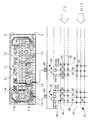
図4及び5に、本発明による制御装置の2つの実施形態が示されており、制御装置はいずれも参照符号21によって指示されている。
制御装置21は、もっぱら一例として、図1及び2との関連で説明したLCDセルによって代表されるようなLCDセルを制御するためのものである。従って、この制御装置21で図1及び2との関連で説明したものと同じ構成要素は、図1及び2と同じ参照符号で指示されている。
【0020】
図4に示す実施形態の制御装置21について説明する。
図示の制御装置21は、LCDセル1の複数のコンタクトパッド1.3、1.5に接続された複数の端子を有する。図4では、図を明瞭にするために、これらの端子はその中の2つだけが示されており、参照符号22及び23が付されている。
制御装置21は、さらに複数の制御手段(具体的には参照符号33a〜33cで示されている)、複数の多重化手段(具体的には参照符号35で示されている)及び接続路のマトリクス網(具体的には参照符号45、47、49、50、52及び54〜56で示す)を有する。
上記制御手段は、対応する記号及び/またはセグメントの表示または消去を制御することが可能な信号をLCDセル1の第1及び第2の電極へ供給するよう構成されている。
【0021】
好ましくは、これらの各制御手段は周知のDラッチ、すなわち供給される制御信号の“0”または“1”の論理状態を記憶することが可能な手段を用いて構成する。
各多重化手段は、接続端子の1つと制御手段の中の3つとの間に接続され、端子と制御手段の1つとの間を逐次電気的に接続するよう構成されている。
【0022】
一例として、3つの位相を含む多重化サイクルの間に、端子22に接続することができる制御手段33a〜33cは、多重化手段35、接続端子22、コンタクトパッド1.3及び導電路1.4を介して電極1.1a〜1.1cの制御信号をそれぞれ供給する。通常、電極1.1aは多重化サイクルの第1の位相の間に手段33aによって制御され、電極1.1bは第2の位相の間に手段33bによって制御され、電極1.1cは第3の位相の間に手段33cによって制御される。
好ましくは、各多重化手段としては、それぞれ周知のマルチプレクサが使用される。
【0023】
接続路のマトリクス網は、行(具体的には参照符号45及び47で示されている)及び列(具体的には参照符号49及び50で示されている)を有する。好ましくは、接続路は金属ストリップの蒸着によって形成される。
【0024】
このマトリックス網の列は制御手段に接続される。例えば、列49及び50は制御手段33aに接続される。
このマトリクス網の行は、一方では多重化サイクルの3つの位相の中の1つの位相の間に制御手段が接続される電極にその制御手段によって供給される制御信号の状態を変更するための制御手段の選択されたアドレスを表し、他方ではそのような状態のデータを表す2値信号(“0”または“1”)を供給する中央処理装置(図示省略の)に接続される。電極の制御信号の“0”状態は、LCDセルの不活性化、すなわち上記のような電極によって形成される記号及び/またはセグメントの消去を表し、また“1”状態はそのような電極の活性化、すなわちこの記号及び/またはセグメントの表示を表すということは想起されよう。一例として、行45は状態データを内容とする信号を供給し、行47は選択されたアドレスを内容とする信号を供給する。
【0025】
制御装置21は、さらに、マトリクス網の行と列の間の各交点に設けられた複数のスイッチ手段52を有する。
各スイッチ手段52は、所定の回路設計に従って、導通の「ON」状態あるいは非導通の「OFF」状態に永久的に切り換えることが可能なように構成されている。各スイッチ手段52のONあるいはOFF状態は、黒丸あるいは白丸の記号によってそれぞれ表されている。一例として、行45と列50との間のスイッチ手段52は、それらの手段がON状態にあることを意味する黒丸によって表されている。言い換えると、行45は列50に接続され、制御手段33aは、行45によって供給される信号中に含まれるデータを受け取る。また、例えば行47と列49との間のスイッチ手段52は、それらの制御手段がOFF状態であることを意味する白丸によって表されている。換言すれば、行45は列50と接続されておらず、制御手段 33aは、行47によって供給される信号に含まれるアドレスを受け取らない。
【0026】
好ましくは、各スイッチ手段52は、マトリクス網の行と列の間の各交点にメタライゼーションを形成するか、あるいはそのようなメタライゼーションを形成しないことによって作り込まれる。
【0027】
当業者ならば、制御装置の21の制御手段、マトリクス網及びスイッチ手段は、従来の半導体プロダクト製造プロセスに従って半導体基板中にモノリシック状に形成することができるということは理解されよう。本願明細書においては、この種のプロセスは、このような製品の製造分野の知識を有する当業者にとって自明であると考える。従って、本願明細書においては、図4に示すような制御装置を製造するこの種のプロセスについては説明を省略する。
【0028】
スイッチ手段52の1つの長所は、異なる電極に同じ制御信号を供給してセグメント及び/または記号の同時表示を起こさせる経路が接続されるようにして、制御しようとするLCDセル1に応じて回路設計に従い切り換えることができるということである。換言すれば、制御装置21は、制御されるLCDセルの関数として合理化され、同一データの重複を少なくするよう作用する構成を有する。
【0029】
次に、本発明によ制御装置の第2の実施形態について図5を参照して説明する。図5には、LCDセル1の「OFF」と「ON」記号の合理化されたコマンドを供給する本発明の装置が示されている。
図5で示す制御装置21は図4で示すものとほぼ同じであることは理解されよう。従って、図1及び2との関連で説明したものと同じこの制御装置21の構成要素は同じ参照符号で指示されている。
【0030】
しかしながら、図5に示す上記マトリクス網の回路設計の構成は、上記の合理化されたコマンドを実現する目的の点で、図4に示す構成と異なっているということに留意すべきである。
従って、図5に示すように、行47と列49との交点に設けられたスイッチ手段52は、行47と列54の交点に設けられたスイッチ手段と同様にON状態である。そのため、端子22と接続することが可能な制御手段33a及び端子23と接続することが可能な制御手段33cは上記処理装置23から同じ選択されたアドレスを受け取ることができる。逆に、行45と列50の交点に設けられたスイッチ手段52はON状態であり、他方行45と列55の交点に設けられたスイッチ手段はOFF状態にある。
【0031】
次に、図5の制御装置の動作を、LCDセル1によって「OFF」と「ON」記号を交互に表示しなければならず、最初は「ON」記号が表示されていると仮定して、「OFF」記号の表示をコマンドで指示したい前述の場合で説明する。
【0032】
第1の多重化サイクルの第1の位相の間に、手段33aは、「OFF」記号の消去を指示する“0”信号を端子22を介して供給し、その第3の位相の間には、手段33cが「ON」記号の表示を指示する“1”信号を端子23を介して供給し、上記処理装置が、「OFF」記号の表示を指示することが可能な制御手段33a及び「ON」記号の消去を指示することが可能な制御手段33cに対応するよう選択されるアドレスを行47を介して制御装置21に供給する。このようなアドレス供給は、以下に説明するようにして、状態データにより上記制御手段のリプログラミングを許可するよう作用する。同時に、上記処理装置は、行56を介して「ON」記号の消去を表す状態データ(すなわち“0”)を供給し、行45を介して「OFF」記号の表示を表す状態データ(すなわち“1”)を供給する。
【0033】
このように、この制御手段のリプログラミングに続く多重化サイクルの第1の位相の間に、手段 33aが端子22を介して「OFF」記号の表示を指示する“1”信号を供給し、このサイクルの第3の位相の間に制御手段 33cが端子23を介して「ON」記号の消去を指示する“0”信号を供給する。
換言すれば、制御装置21はLCDセル1の「OFF」記号の表示のコマンドを実現するのに2多重化サイクルしか必要とせず、これによって、前述の従来技術と比較して、この制御装置の制御が合理化されたものとなる。
【0034】
当業者にとっては、上に詳細に説明した制御装置には、本発明の範囲を逸脱することなく種々の修正態様をなすことが可能なことは言うまでもない。一例として、制御しようとするLCDセルの記号及び/またはセグメントと同じ数だけ接続端子を具備し、それらの各端子が単一の記号またはセグメントに接続されるようにして、LCDセルの無多重化制御を実現する制御装置を本発明の範囲内で実施することも可能である。
【図面の簡単な説明】
【図1】 従来のLCDセルの第1の基板の前面を示す平面図である。
【図2】 従来のLCDセルの第2の基板の裏面を示す図1同様の平面図である。
【図3】 従来のLCDセルに接続された制御装置の構成を示すブロック図である。
【図4】 図1及び2と関連して上に説明したLCDセルに接続された本発明の制御装置の第1の実施形態を示す説明図である。
【図5】 図1及び2と関連して上に説明したLCDセルに接続された本発明の制御装置の第2の実施形態を示す説明図である。
【符号の説明】
21 マトリックス網、22,23 端子、33a〜33c 制御手段、35制御装置、45、47 行、49、50 列、52 スイッチ手段。[0001]
BACKGROUND OF THE INVENTION
The present invention relates to an apparatus for controlling a liquid crystal cell, and more particularly to an apparatus for controlling a liquid crystal display cell used to display segments and / or symbols.
In the present specification, such a cell is referred to as an “LCD” (liquid crystal display).
[0002]
[Prior art]
Such LCD cells are widely used in many applications, particularly in the fields of small calculators, watches and instrumentation.
A conventional LCD cell is disclosed in French Patent No. 2,712,109. FIGS. 1 and 2 of the accompanying drawings of the present application show the front surface of the first substrate 1 and the back surface of the second substrate 2 of the LCD cell disclosed in the above-mentioned French patent, respectively.
[0003]
The substrate or plate 1 is designated by a first electrode (specifically with reference numbers 1.1 and 1.1a to 1.1c) forming symbols such as “ON”, “OFF” and “AUTO”. Electrode) and a second electrode (specifically the electrode indicated by reference numeral 1.2) that forms a segment organized in the shape of an “8” to provide a numeric display. As an example, electrode 1.1a forms the “OFF” symbol, and electrodes 1.1b and 1.1c form two segments in the same segment group of eight shapes.
[0004]
As will be described later, the substrate or plate 2 comprises a third electrode (specifically an electrode indicated by reference numeral 2.1) arranged to face the first electrode of plate 1, and It has the 4th electrode (specifically the electrode designated by the referential mark 2.2) which can be arrange | positioned so that the 2nd electrode of the plate 1 may be opposed.
[0005]
Plates 1 and 2 together with these two plates 1 and 2 are separated from each other by a sealing
Further, the plate 1 has a plurality of contact pads (specifically indicated by reference numerals 1.3 and 1.5) arranged on the outside of the
[0006]
A brief reminder will be given on how to activate or deactivate the liquid crystal layer 4 of the LCD cell 1.
A voltage is applied between one of the first (or second) electrodes of the plate 1 and the electrode of the plate 2 disposed opposite to the electrode of the plate 1. As a result, an electric field is formed between these two electrodes, and this electric field acts on the component formed by the liquid crystal between such electrodes, so that the transmission characteristics of light passing through that part And change the reflection characteristics.
Typically, for an LCD cell, an LCD cell is said to be activated when the light is blocked and the symbol and / or segment corresponding to that portion is displayed, and the light is reflected and the portion's symbol and / or Or the LCD cell is deactivated when the segment disappears (normal contrast mode).
[0007]
In general, an LCD cell as described above in connection with FIGS. 1 and 2 is configured to provide a control voltage (or control signal) that can cause the LCD cell to be activated or deactivated. It is connected to a normal control device or drive circuit.
Such a control device generally provides multiplexed control signals for the purpose of reducing the number of wires between the control device and the LCD cell.
[0008]
To implement multiplexing of these control signals, referring again to FIGS. 1 and 2, each contact pad of plate 1 is connected to three of the first and second electrodes of the plate. As an example, the contact pad 1.3 connected to the electrodes 1.1a-1.1c can sequentially receive three corresponding signals from the control device. Normally, electrode 1.1a receives a first signal ("1" or "0") from the controller during the first phase of the multiplexing cycle, and the "OFF" symbol formed by electrode 1.1a Each is displayed or disappeared. Similarly, electrode 1.1b receives a second signal ("1" or "0") during the second phase of the multiplexing cycle and displays each segment formed by electrode 1.1b. Otherwise, the electrode 1.1c receives a third signal ("1" or "0") during the third phase of the multiplexing cycle and each segment formed by the electrode 1.1c Display or turn off.
[0009]
[0010]
Now consider the case where such a control device is connected to the LCD cell described in connection with FIGS. 1 and 2 and is used to control the activation or deactivation of the LCD cell. For example, it is assumed that an “ON” symbol is displayed first, and that the display of the “OFF” symbol is desired to be indicated by a command.
[0011]
In this case, the
First, in order to know the display state of the “ON” symbol, the first cycle is to read the state (“0” or “1”) of the control means of each of the three electrodes connected to the contact pad 1.5. Assigned. The second cycle is assigned to the operation of erasing the state stored in the control means and read during the first cycle. The third cycle is assigned to write a “0” state to the control means of the electrode forming the “ON” symbol and to instruct the erase of that symbol with a command. The fourth cycle is assigned to the operation of reading the state of the control means of each electrode of 1.1a to 1.1c. As assumed here, if the “OFF” symbol is not initially displayed, the fifth and sixth cycles are continued after the fourth cycle. The fifth cycle is assigned to erase the “0” state from the control means of the electrode 1.1a, and the sixth cycle writes the “1” state to this control means and displays the “OFF” symbol as a command. Assigned to directing.
[0012]
[Problems to be solved by the invention]
One drawback of the control device as described above is that the manufacturer cannot adapt the assignment of commands to the LCD cells in a simple and rational way to control the display of the desired message. is there. This is because the LCD cell has the same type as described in connection with FIGS. 1 and 2, ie segments and / or symbols that it wants to display periodically in applications such as watches, instrumentation and electronic games. An LCD cell becomes a more negative factor.
[0013]
In addition, if such a control device is built monolithically on a semiconductor substrate, new constraints such as the complexity of the structure, the required space and cost associated with the manufacture of the integrated structure. Conditions and problems arise.
[0014]
Accordingly, one object of the present invention is to provide a control device for an LCD cell, particularly a control device capable of rationally controlling a predetermined LCD cell, eliminating the difficulties and disadvantages of the conventional devices described above. It is in.
Another object of the present invention is to provide a control device that can be built into a semiconductor substrate with a minimum occupied surface area.
Another object of the present invention is to provide a control device for an LCD as described above, which can be manufactured by a conventional manufacturing process in the semiconductor industry.
Another object of the present invention is to provide a control device that overcomes the limitations and problems of conventional semiconductor technology with respect to complexity, required space and cost.
[0015]
[Means for Solving the Problems]
The present invention made to achieve the above and other objects is a control device for a liquid crystal display cell, which is a segment formed of a plurality of electrodes in a display cell in response to a control signal supplied by the control device. And / or in a control device for displaying a predetermined message by means of symbols: a plurality of control means for supplying the control signal to the electrodes; a column connected to the control means and a row being said control signal and address A matrix network of connection paths connected to receive data signals representing signals, and further provided at each intersection of a row and a column of the matrix network according to a predetermined circuit design as a function of the cell It must be displayed periodically so that it can be permanently switched to the conducting or non-conducting state to obtain the predetermined message. Characterized by comprising a plurality of switching means configured to allow simultaneous display of segments and / or symbols.
[0016]
One advantage of the switch means of the control device according to the invention is that control is provided such that the same signal path is connected which can control different electrodes to cause simultaneous display of segments and / or symbols. It is possible to switch according to the circuit design according to the LCD cell to be attempted. In other words, the control device of the present invention is configured according to the LCD cell to be controlled, acts to reduce duplication of the same data, and is used for addresses and data supplied to the control means of the device. The storage device has a structure that can be relatively small. As a result, power consumption is reduced.
[0017]
One advantage of the integrated structure with the control device of the present invention is that it is formed of components that can be manufactured during the implementation of a conventional manufacturing process.
One advantage of such a structure is that it can receive and provide signals compatible with conventional central processing units.
[0018]
DETAILED DESCRIPTION OF THE INVENTION
These and other objects, features and advantages of the present invention will become more apparent by reading the following detailed description of two embodiments of the present invention, which are presented solely for illustrative purposes, with reference to the accompanying drawings. To be able to understand.
[0019]
FIGS. 4 and 5 show two embodiments of the control device according to the invention, both of which are indicated by
The
[0020]
The
The illustrated
The
The control means is configured to supply the first and second electrodes of the LCD cell 1 with a signal capable of controlling the display or erasure of the corresponding symbol and / or segment.
[0021]
Preferably, each of these control means is configured using a well-known D latch, that is, means capable of storing a logic state of “0” or “1” of the supplied control signal.
Each multiplexing means is connected between one of the connection terminals and three of the control means, and is configured to sequentially electrically connect between the terminal and one of the control means.
[0022]
As an example, the control means 33a-33c that can be connected to the terminal 22 during a multiplexing cycle including three phases are the multiplexing means 35, the
Preferably, a known multiplexer is used as each multiplexing means.
[0023]
The matrix network of connection paths has rows (specifically indicated by
[0024]
This matrix network column is connected to the control means. For example,
The rows of this matrix network, on the one hand, are controls for changing the state of the control signal supplied by the control means to the electrode to which the control means is connected during one of the three phases of the multiplexing cycle. It is connected to a central processing unit (not shown) which represents a selected address of the means and on the other hand supplies a binary signal ("0" or "1") representing such state data. The “0” state of the electrode control signal represents the deactivation of the LCD cell, ie the erasure of the symbols and / or segments formed by the electrodes as described above, and the “1” state the activation of such electrodes. It will be recalled that this represents a representation of this symbol and / or segment. As an example,
[0025]
The
Each switch means 52 is configured to be able to be permanently switched to a conductive “ON” state or a non-conductive “OFF” state according to a predetermined circuit design. The ON or OFF state of each switch means 52 is represented by a black circle or white circle symbol, respectively. As an example, the switch means 52 between the
[0026]
Preferably, each switch means 52 is made by forming a metallization at each intersection between the rows and columns of the matrix network or by not forming such a metallization.
[0027]
Those skilled in the art will appreciate that the 21 control means, matrix network and switch means of the controller can be formed monolithically in a semiconductor substrate according to a conventional semiconductor product manufacturing process. In this specification, this type of process is considered obvious to those skilled in the art having knowledge in the field of manufacturing such products. Therefore, in this specification, description of this type of process for manufacturing a control device as shown in FIG. 4 is omitted.
[0028]
One advantage of the switch means 52 is that a circuit is connected depending on the LCD cell 1 to be controlled so that the same control signal is supplied to the different electrodes to cause the simultaneous display of segments and / or symbols to be connected. It can be switched according to the design. In other words, the
[0029]
Next, a second embodiment of the control device according to the present invention will be described with reference to FIG. FIG. 5 shows a device according to the invention for supplying a streamlined command of the “OFF” and “ON” symbols of the LCD cell 1.
It will be understood that the
[0030]
However, it should be noted that the circuit design configuration of the matrix network shown in FIG. 5 is different from the configuration shown in FIG. 4 in terms of the purpose of realizing the streamlined command.
Therefore, as shown in FIG. 5, the switch means 52 provided at the intersection of the
[0031]
Next, the operation of the control device of FIG. 5 assumes that the “OFF” and “ON” symbols must be displayed alternately by the LCD cell 1, and initially the “ON” symbol is displayed, The case where the “OFF” symbol display is to be instructed by a command will be described.
[0032]
During the first phase of the first multiplexing cycle, the
[0033]
Thus, during the first phase of the multiplexing cycle following the reprogramming of this control means, means 33a provides a "1" signal indicating the display of the "OFF" symbol via
In other words, the
[0034]
It goes without saying for those skilled in the art that various modifications can be made to the control device described in detail above without departing from the scope of the present invention. As an example, there is no multiplexing of LCD cells, with as many connection terminals as there are symbols and / or segments of the LCD cell to be controlled, each terminal being connected to a single symbol or segment. It is also possible to implement a control device for realizing the control within the scope of the present invention.
[Brief description of the drawings]
FIG. 1 is a plan view showing a front surface of a first substrate of a conventional LCD cell.
FIG. 2 is a plan view similar to FIG. 1, showing a back surface of a second substrate of a conventional LCD cell.
FIG. 3 is a block diagram showing a configuration of a control device connected to a conventional LCD cell.
4 is an illustration showing a first embodiment of the control device of the present invention connected to the LCD cell described above in connection with FIGS. 1 and 2. FIG.
FIG. 5 is an illustration showing a second embodiment of the control device of the present invention connected to the LCD cell described above in connection with FIGS. 1 and 2;
[Explanation of symbols]
21 Matrix network, 22, 23 terminals, 33a to 33c control means, 35 control device, 45, 47 rows, 49, 50 columns, 52 switch means.
Claims (3)
上記電極に上記制御信号を供給するための複数の制御手段(33a;33b;33c)であって、上記電極群に対応した群を形成する複数の制御手段と;
列(49;50)が上記制御手段に接続されており、行(45;47)が上記制御信号を形成するためのアドレス信号とデータ信号を受け取るように接続された接続路のマトリクス網(45;47;49;50)と;
を具備し、
さらに、上記マトリクス網の行と列との各交点に設けられ、上記液晶ディスプレイセルの所定の回路設計に従い導通状態または非導通状態に永久的に切り換えられて、上記所定のメッセージを得るために、上記異なる群に属する制御手段を同時に選択することを可能にするように構成された複数のスイッチ手段(52)を具備し、
上記制御手段(33a;33b;33c)、上記マトリクス網(45;47;49;50)及び上記スイッチ手段(52)が半導体基板でモノリシック状に形成され、
上記各スイッチ手段(52)は、上記マトリクス網の行と列との各交点が導通状態になるようメタライゼーションを形成することにより、または非導通状態になるようメタライゼーションを形成しないことにより構成されることを特徴とする制御装置。The liquid crystal controller of the display cell (1) (21), in response to a control signal supplied by the control unit, to the liquid crystal display cell, a plurality of electrodes (1 to form a connection has been electrode group to each other .1a; 1.1b; 1.1c) controller for displaying a predetermined message by the segment and / or symbols formed by the (21):
A plurality of control means (33a; 33b; 33c) for supplying the control signal to the electrodes, and a plurality of control means for forming a group corresponding to the electrode group ;
Columns (49; 50) are connected to the control means, and rows (45; 47) are connected matrix networks (45) connected to receive address signals and data signals for forming the control signals. 47; 49; 50) and;
Comprising
Furthermore, provided at each intersection of a row and column of the matrix network, permanently switched to the conductive state or a nonconductive state in accordance with the circuit design of the constant at the above liquid crystal display cell, order to obtain the predetermined message A plurality of switch means (52) configured to enable simultaneous selection of the control means belonging to the different groups ,
The control means (33a; 33b; 33c) , the matrix network (45; 47; 49; 50) and the switch means (52) are formed monolithically on a semiconductor substrate,
Each of the switch means (52) is configured by forming the metallization so that each intersection of the row and column of the matrix network is conductive, or by not forming the metallization so as to be non-conductive. A control device.
Applications Claiming Priority (5)
| Application Number | Priority Date | Filing Date | Title |
|---|---|---|---|
| CH81298 | 1998-04-06 | ||
| CH0812/98 | 1998-04-06 | ||
| EP0812/98 | 1998-06-05 | ||
| EP98110269.2 | 1998-06-05 | ||
| EP19980110269 EP0949549B1 (en) | 1998-04-09 | 1998-06-05 | Astronomical clock |
Publications (2)
| Publication Number | Publication Date |
|---|---|
| JP2000066629A JP2000066629A (en) | 2000-03-03 |
| JP5036926B2 true JP5036926B2 (en) | 2012-09-26 |
Family
ID=25685763
Family Applications (1)
| Application Number | Title | Priority Date | Filing Date |
|---|---|---|---|
| JP09866299A Expired - Fee Related JP5036926B2 (en) | 1998-04-06 | 1999-04-06 | Liquid crystal display cell control device |
Country Status (1)
| Country | Link |
|---|---|
| JP (1) | JP5036926B2 (en) |
Family Cites Families (5)
| Publication number | Priority date | Publication date | Assignee | Title |
|---|---|---|---|---|
| JPS56168588A (en) * | 1980-05-30 | 1981-12-24 | Citizen Watch Co Ltd | Digital display type electronic timepiece |
| JPS57178289A (en) * | 1981-04-27 | 1982-11-02 | Hitachi Ltd | Display driver |
| JPS59193831U (en) * | 1983-06-09 | 1984-12-22 | 株式会社フジクラ | Optical fiber base material manufacturing equipment |
| JP3139892B2 (en) * | 1993-09-13 | 2001-03-05 | 株式会社東芝 | Data selection circuit |
| JP2791415B2 (en) * | 1995-02-13 | 1998-08-27 | カシオ計算機株式会社 | LCD drive system |
-
1999
- 1999-04-06 JP JP09866299A patent/JP5036926B2/en not_active Expired - Fee Related
Also Published As
| Publication number | Publication date |
|---|---|
| JP2000066629A (en) | 2000-03-03 |
Similar Documents
| Publication | Publication Date | Title |
|---|---|---|
| US4443062A (en) | Multi-layer display device with nonactive display element groups | |
| US5821688A (en) | Flexible panel display having thin film transistors driving polymer light-emitting diodes | |
| US6636194B2 (en) | Electrooptic device and electronic equipment | |
| US4851827A (en) | Matrix display devices with redundant driving transistor arrangement for improved fault tolerance | |
| JPH0525440B2 (en) | ||
| EP1145075B8 (en) | Sealing of cells having active backplanes | |
| US4142226A (en) | Multi-contact electrical edge connector for display panels | |
| JP5036926B2 (en) | Liquid crystal display cell control device | |
| US4212011A (en) | Multimode liquid crystal display | |
| US20030161126A1 (en) | Spacers for cells having spaced opposed substrates | |
| US5003302A (en) | Dual addressing transistor active matrix display screen | |
| KR20010028536A (en) | Liquid crystal display device | |
| JPS5912179B2 (en) | liquid crystal display device | |
| US6344838B1 (en) | Control device for a liquid crystal display cell | |
| WO2003052732A1 (en) | Programmable row selection in liquid crystal display drivers | |
| JP4803902B2 (en) | Display device | |
| US6839119B2 (en) | Display device | |
| EP0479915B1 (en) | Compact portable computer | |
| JPS59214075A (en) | Ic substrate for active panel | |
| WO2002045016A3 (en) | Balanced binary color and digitally controlled waveform drive methods for graphic display | |
| JPH09106264A (en) | Driving circuit for fluorescent display device | |
| TWI838796B (en) | Signal control method, controller chip and touch screen | |
| EP0949531B1 (en) | Driver device for a liquid crystal display cell | |
| JP2683169B2 (en) | Semiconductor device | |
| JP2001350154A (en) | Liquid crystal display device and electronic device using the same |
Legal Events
| Date | Code | Title | Description |
|---|---|---|---|
| A621 | Written request for application examination |
Free format text: JAPANESE INTERMEDIATE CODE: A621 Effective date: 20060327 |
|
| A977 | Report on retrieval |
Free format text: JAPANESE INTERMEDIATE CODE: A971007 Effective date: 20090624 |
|
| A131 | Notification of reasons for refusal |
Free format text: JAPANESE INTERMEDIATE CODE: A131 Effective date: 20090707 |
|
| A521 | Written amendment |
Free format text: JAPANESE INTERMEDIATE CODE: A523 Effective date: 20091001 |
|
| A02 | Decision of refusal |
Free format text: JAPANESE INTERMEDIATE CODE: A02 Effective date: 20100720 |
|
| A521 | Written amendment |
Free format text: JAPANESE INTERMEDIATE CODE: A523 Effective date: 20101122 |
|
| A911 | Transfer of reconsideration by examiner before appeal (zenchi) |
Free format text: JAPANESE INTERMEDIATE CODE: A911 Effective date: 20101130 |
|
| A912 | Removal of reconsideration by examiner before appeal (zenchi) |
Free format text: JAPANESE INTERMEDIATE CODE: A912 Effective date: 20110610 |
|
| A521 | Written amendment |
Free format text: JAPANESE INTERMEDIATE CODE: A523 Effective date: 20120507 |
|
| A01 | Written decision to grant a patent or to grant a registration (utility model) |
Free format text: JAPANESE INTERMEDIATE CODE: A01 |
|
| A61 | First payment of annual fees (during grant procedure) |
Free format text: JAPANESE INTERMEDIATE CODE: A61 Effective date: 20120704 |
|
| FPAY | Renewal fee payment (event date is renewal date of database) |
Free format text: PAYMENT UNTIL: 20150713 Year of fee payment: 3 |
|
| R150 | Certificate of patent or registration of utility model |
Free format text: JAPANESE INTERMEDIATE CODE: R150 |
|
| LAPS | Cancellation because of no payment of annual fees |