JP5031493B2 - Manufacturing method of substrate for inkjet head - Google Patents
Manufacturing method of substrate for inkjet head Download PDFInfo
- Publication number
- JP5031493B2 JP5031493B2 JP2007231352A JP2007231352A JP5031493B2 JP 5031493 B2 JP5031493 B2 JP 5031493B2 JP 2007231352 A JP2007231352 A JP 2007231352A JP 2007231352 A JP2007231352 A JP 2007231352A JP 5031493 B2 JP5031493 B2 JP 5031493B2
- Authority
- JP
- Japan
- Prior art keywords
- hole
- substrate
- holes
- row
- tan
- Prior art date
- Legal status (The legal status is an assumption and is not a legal conclusion. Google has not performed a legal analysis and makes no representation as to the accuracy of the status listed.)
- Active
Links
- 239000000758 substrate Substances 0.000 title claims description 119
- 238000004519 manufacturing process Methods 0.000 title claims description 34
- 238000005530 etching Methods 0.000 claims description 52
- 230000001681 protective effect Effects 0.000 claims description 47
- 238000000034 method Methods 0.000 claims description 41
- 239000007788 liquid Substances 0.000 claims description 9
- 239000002184 metal Substances 0.000 claims description 2
- 229910052751 metal Inorganic materials 0.000 claims description 2
- 238000007599 discharging Methods 0.000 claims 3
- 239000011148 porous material Substances 0.000 claims 2
- XUIMIQQOPSSXEZ-UHFFFAOYSA-N Silicon Chemical compound [Si] XUIMIQQOPSSXEZ-UHFFFAOYSA-N 0.000 description 54
- 229910052710 silicon Inorganic materials 0.000 description 53
- 239000010703 silicon Substances 0.000 description 53
- 230000015572 biosynthetic process Effects 0.000 description 14
- 238000000206 photolithography Methods 0.000 description 8
- 239000000463 material Substances 0.000 description 4
- WGTYBPLFGIVFAS-UHFFFAOYSA-M tetramethylammonium hydroxide Chemical compound [OH-].C[N+](C)(C)C WGTYBPLFGIVFAS-UHFFFAOYSA-M 0.000 description 4
- 238000001312 dry etching Methods 0.000 description 3
- 238000003754 machining Methods 0.000 description 3
- 229910004200 TaSiN Inorganic materials 0.000 description 2
- 241000425571 Trepanes Species 0.000 description 2
- 238000010521 absorption reaction Methods 0.000 description 2
- 230000000149 penetrating effect Effects 0.000 description 2
- ATJFFYVFTNAWJD-UHFFFAOYSA-N Tin Chemical compound [Sn] ATJFFYVFTNAWJD-UHFFFAOYSA-N 0.000 description 1
- 239000012670 alkaline solution Substances 0.000 description 1
- 239000011248 coating agent Substances 0.000 description 1
- 238000000576 coating method Methods 0.000 description 1
- 238000007796 conventional method Methods 0.000 description 1
- 230000003247 decreasing effect Effects 0.000 description 1
- 238000005553 drilling Methods 0.000 description 1
- 238000000059 patterning Methods 0.000 description 1
- 238000004904 shortening Methods 0.000 description 1
- 239000000243 solution Substances 0.000 description 1
- 238000001039 wet etching Methods 0.000 description 1
Images


Classifications
-
- B—PERFORMING OPERATIONS; TRANSPORTING
- B41—PRINTING; LINING MACHINES; TYPEWRITERS; STAMPS
- B41J—TYPEWRITERS; SELECTIVE PRINTING MECHANISMS, i.e. MECHANISMS PRINTING OTHERWISE THAN FROM A FORME; CORRECTION OF TYPOGRAPHICAL ERRORS
- B41J2/00—Typewriters or selective printing mechanisms characterised by the printing or marking process for which they are designed
- B41J2/005—Typewriters or selective printing mechanisms characterised by the printing or marking process for which they are designed characterised by bringing liquid or particles selectively into contact with a printing material
- B41J2/01—Ink jet
- B41J2/135—Nozzles
- B41J2/16—Production of nozzles
- B41J2/1601—Production of bubble jet print heads
- B41J2/1603—Production of bubble jet print heads of the front shooter type
-
- B—PERFORMING OPERATIONS; TRANSPORTING
- B41—PRINTING; LINING MACHINES; TYPEWRITERS; STAMPS
- B41J—TYPEWRITERS; SELECTIVE PRINTING MECHANISMS, i.e. MECHANISMS PRINTING OTHERWISE THAN FROM A FORME; CORRECTION OF TYPOGRAPHICAL ERRORS
- B41J2/00—Typewriters or selective printing mechanisms characterised by the printing or marking process for which they are designed
- B41J2/005—Typewriters or selective printing mechanisms characterised by the printing or marking process for which they are designed characterised by bringing liquid or particles selectively into contact with a printing material
- B41J2/01—Ink jet
- B41J2/135—Nozzles
- B41J2/14—Structure thereof only for on-demand ink jet heads
- B41J2/14016—Structure of bubble jet print heads
- B41J2/14145—Structure of the manifold
-
- B—PERFORMING OPERATIONS; TRANSPORTING
- B41—PRINTING; LINING MACHINES; TYPEWRITERS; STAMPS
- B41J—TYPEWRITERS; SELECTIVE PRINTING MECHANISMS, i.e. MECHANISMS PRINTING OTHERWISE THAN FROM A FORME; CORRECTION OF TYPOGRAPHICAL ERRORS
- B41J2/00—Typewriters or selective printing mechanisms characterised by the printing or marking process for which they are designed
- B41J2/005—Typewriters or selective printing mechanisms characterised by the printing or marking process for which they are designed characterised by bringing liquid or particles selectively into contact with a printing material
- B41J2/01—Ink jet
- B41J2/135—Nozzles
- B41J2/16—Production of nozzles
- B41J2/1621—Manufacturing processes
- B41J2/1626—Manufacturing processes etching
- B41J2/1628—Manufacturing processes etching dry etching
-
- B—PERFORMING OPERATIONS; TRANSPORTING
- B41—PRINTING; LINING MACHINES; TYPEWRITERS; STAMPS
- B41J—TYPEWRITERS; SELECTIVE PRINTING MECHANISMS, i.e. MECHANISMS PRINTING OTHERWISE THAN FROM A FORME; CORRECTION OF TYPOGRAPHICAL ERRORS
- B41J2/00—Typewriters or selective printing mechanisms characterised by the printing or marking process for which they are designed
- B41J2/005—Typewriters or selective printing mechanisms characterised by the printing or marking process for which they are designed characterised by bringing liquid or particles selectively into contact with a printing material
- B41J2/01—Ink jet
- B41J2/135—Nozzles
- B41J2/16—Production of nozzles
- B41J2/1621—Manufacturing processes
- B41J2/1626—Manufacturing processes etching
- B41J2/1629—Manufacturing processes etching wet etching
-
- B—PERFORMING OPERATIONS; TRANSPORTING
- B41—PRINTING; LINING MACHINES; TYPEWRITERS; STAMPS
- B41J—TYPEWRITERS; SELECTIVE PRINTING MECHANISMS, i.e. MECHANISMS PRINTING OTHERWISE THAN FROM A FORME; CORRECTION OF TYPOGRAPHICAL ERRORS
- B41J2/00—Typewriters or selective printing mechanisms characterised by the printing or marking process for which they are designed
- B41J2/005—Typewriters or selective printing mechanisms characterised by the printing or marking process for which they are designed characterised by bringing liquid or particles selectively into contact with a printing material
- B41J2/01—Ink jet
- B41J2/135—Nozzles
- B41J2/16—Production of nozzles
- B41J2/1621—Manufacturing processes
- B41J2/1631—Manufacturing processes photolithography
-
- B—PERFORMING OPERATIONS; TRANSPORTING
- B41—PRINTING; LINING MACHINES; TYPEWRITERS; STAMPS
- B41J—TYPEWRITERS; SELECTIVE PRINTING MECHANISMS, i.e. MECHANISMS PRINTING OTHERWISE THAN FROM A FORME; CORRECTION OF TYPOGRAPHICAL ERRORS
- B41J2/00—Typewriters or selective printing mechanisms characterised by the printing or marking process for which they are designed
- B41J2/005—Typewriters or selective printing mechanisms characterised by the printing or marking process for which they are designed characterised by bringing liquid or particles selectively into contact with a printing material
- B41J2/01—Ink jet
- B41J2/135—Nozzles
- B41J2/16—Production of nozzles
- B41J2/1621—Manufacturing processes
- B41J2/1632—Manufacturing processes machining
- B41J2/1634—Manufacturing processes machining laser machining
-
- B—PERFORMING OPERATIONS; TRANSPORTING
- B41—PRINTING; LINING MACHINES; TYPEWRITERS; STAMPS
- B41J—TYPEWRITERS; SELECTIVE PRINTING MECHANISMS, i.e. MECHANISMS PRINTING OTHERWISE THAN FROM A FORME; CORRECTION OF TYPOGRAPHICAL ERRORS
- B41J2/00—Typewriters or selective printing mechanisms characterised by the printing or marking process for which they are designed
- B41J2/005—Typewriters or selective printing mechanisms characterised by the printing or marking process for which they are designed characterised by bringing liquid or particles selectively into contact with a printing material
- B41J2/01—Ink jet
- B41J2/135—Nozzles
- B41J2/16—Production of nozzles
- B41J2/1621—Manufacturing processes
- B41J2/1637—Manufacturing processes molding
- B41J2/1639—Manufacturing processes molding sacrificial molding
Landscapes
- Engineering & Computer Science (AREA)
- Manufacturing & Machinery (AREA)
- Physics & Mathematics (AREA)
- Optics & Photonics (AREA)
- Particle Formation And Scattering Control In Inkjet Printers (AREA)
Description
本発明は、熱エネルギーを用いてインクを吐出させるインクジェットヘッド用基板の製造方法に関する。 The present invention relates to a method for manufacturing an ink jet head substrate that ejects ink using thermal energy.
インク吐出圧発生素子の上方に向けてインク滴を吐出するインクジェットヘッド(以下、サイドシュータ型ヘッド)が知られている。このタイプのインクジェットヘッドでは、インク吐出圧発生素子が形成された基板に貫通スロット(インク供給口)を設け、インク吐出圧発生素子が形成された面とは反対側の面よりインクを供給する方式が採られている。 2. Related Art Inkjet heads (hereinafter referred to as side shooter type heads) that eject ink droplets toward an ink ejection pressure generating element are known. In this type of inkjet head, a through slot (ink supply port) is provided in a substrate on which an ink discharge pressure generating element is formed, and ink is supplied from a surface opposite to the surface on which the ink discharge pressure generating element is formed. Has been adopted.
この種のインクジェットヘッドのインク供給口形成法として、フォトリソグラフィープロセスによる保護膜のパターニングと異方性エッチングとを組み合わせた方法が開示されている。特許文献1では、シリコン(100)基板の裏面上に保護膜を形成し、フォトリソグラフィープロセスでインク供給口形成部位の保護膜を除去し、強アルカリ溶液中で異方性エッチングすることで、供給口を形成する方法が示されている。この方法では、裏面の保護膜開口寸法を変えることで供給口寸法を決めることができるため、用途に応じて供給口寸法を設定できる利点がある。
しかしながら、この種のインク供給口形成法では、フォトリソグラフィープロセスを用いて保護膜を開口するため、工程数が増加し、生産効率が低いという問題がある。例えば、熱酸化膜を保護膜として用いた場合、熱酸化膜形成、熱酸化膜上へのレジスト塗布、レジストの露光および現像、ウエットエッチングまたはドライエッチングによる熱酸化膜除去、レジストの除去、といったように複数のプロセスが必要となってしまう。 However, this type of ink supply port formation method has a problem that the number of steps increases and the production efficiency is low because the protective film is opened using a photolithography process. For example, when a thermal oxide film is used as a protective film, thermal oxide film formation, resist coating on the thermal oxide film, resist exposure and development, thermal oxide film removal by wet or dry etching, resist removal, etc. Multiple processes are required.
この問題に対し、フォトリソグラフィーを用いることなく、供給口を作製する方法が、特許文献2に開示されている。この方法は、シリコン基板上に保護膜を設け、供給口を形成する部位に保護膜上からレーザ光によって一つの穴(以下、レーザ穴)または、一列に並んだ複数のレーザ穴を形成し、異方性エッチングを行ってレーザ穴を広げて供給口を形成するというものである。レーザ穴からエッチャントが入り込むため、フォトリソグラフィープロセスを用いて保護膜を除去しなくても異方性エッチングを進行させることが可能となっている。しかしながら、この方法では、保護膜の除去寸法がレーザ穴の寸法とほぼ同じになるため、異方性エッチング後に形成される供給口は、そのシリコン基板裏面の開口幅がレーザ穴の寸法とほぼ同じものになってしまう。そのため、この方法では、特許文献1に記載のフォトリソグラフィーを用いたプロセスとは異なり、所望の供給口寸法を得ることができない。レーザ穴を大きくすれば、供給口寸法を大きくすることは可能であるが、一般に、レーザで穴加工を行う場合、スポットサイズを大きくすると、単位面積あたりのエネルギー密度が低下して加工能力が下がってしまう。そのため、加工タクトが増加する問題や、場合によっては途中で掘れなくなったり、加工形状が曲がったりする問題が発生する。
To solve this problem, Patent Document 2 discloses a method for producing a supply port without using photolithography. In this method, a protective film is provided on a silicon substrate, and a single hole (hereinafter referred to as a laser hole) or a plurality of laser holes arranged in a line is formed by laser light from the protective film on a portion where a supply port is formed, An anisotropic etching is performed to widen the laser hole and form a supply port. Since the etchant enters from the laser hole, anisotropic etching can be advanced without removing the protective film using a photolithography process. However, in this method, since the removal dimension of the protective film is almost the same as the dimension of the laser hole, the supply port formed after anisotropic etching has an opening width on the back surface of the silicon substrate substantially the same as the dimension of the laser hole. It becomes a thing. Therefore, in this method, unlike the process using photolithography described in
また、シリコン基板裏面の保護膜除去寸法が小さい状態で異方性エッチングを行うと、裏面開口から逆テーパーの(111)面が形成されるため、基板内部から裏面開口に向かって先細りの形状となってしまう。このような形状では、熱エネルギーを用いてインクを吐出するインクジェットヘッドの場合、熱付与時にインク中に発生した気泡が、先細り部に引っかかって基板外へ排出されにくくなり、インク供給の信頼性が低下する問題が発生することがある。 In addition, when anisotropic etching is performed in a state where the protective film removal dimension on the back surface of the silicon substrate is small, a reversely tapered (111) surface is formed from the back surface opening. turn into. With such a shape, in the case of an ink jet head that ejects ink using thermal energy, bubbles generated in the ink when heat is applied become difficult to be ejected out of the substrate by being caught by the tapered portion, and the ink supply is reliable. Decreasing problems may occur.
然るに、従来のインクジェットヘッドのインク供給口の製造方法においては、工程数を増加させずに、インク供給の信頼性に優れたインク供給口を形成することが困難であった。 However, in the conventional method for manufacturing an ink supply port of an inkjet head, it has been difficult to form an ink supply port excellent in ink supply reliability without increasing the number of steps.
そこで本発明は、上記従来のインクジェットヘッドのインク供給口形成方法が有する問題の少なくとも一つを解決することを目的とし、工程数を増加させずに、インク供給の信頼性に優れたインク供給口の形成方法を提供する。 Accordingly, the present invention aims to solve at least one of the problems of the conventional ink supply port forming method of an inkjet head, and has an ink supply port excellent in ink supply reliability without increasing the number of steps. A forming method is provided.
上記目的を達成するため本発明は、基板にインク供給口を形成することを含むインクジェットヘッド用基板の製造方法であって、
前記基板の表面に保護膜を形成する工程と、該保護膜を貫通して前記基板の内部で留まる第1の未貫通孔を形成する工程と、前記保護膜を貫通して前記基板の内部で留まる第2の未貫通孔を形成する工程と、異方性エッチングにより未貫通孔の間を連通する工程と、を含み、
前記第1の未貫通孔と前記第2の未貫通孔との間の距離をa、前記第2の未貫通孔の深さをdとしたとき、
a×tan54.7°≦ d
なる関係を満たすように前記第2の未貫通孔を形成することを特徴とする。
In order to achieve the above object, the present invention provides a method for manufacturing a substrate for an inkjet head, comprising forming an ink supply port in a substrate,
Forming a protective film on the surface of the substrate, forming a first non-through hole that penetrates the protective film and stays inside the substrate, and penetrates the protective film inside the substrate. Forming a second non-through hole that remains, and communicating between the non-through holes by anisotropic etching,
When the distance between the first non-through hole and the second non-through hole is a, and the depth of the second non-through hole is d,
a × tan 54.7 ° ≦ d
The second non-through hole is formed so as to satisfy the following relationship.
本発明によれば、工程数を増加させずに、インク供給の信頼性に優れたインク供給口の形成方法を提供することができる。 According to the present invention, it is possible to provide a method for forming an ink supply port which is excellent in ink supply reliability without increasing the number of steps.
以下、本発明の最良の実施形態を図面に基づいて説明する。 DESCRIPTION OF EXEMPLARY EMBODIMENTS Hereinafter, the best embodiment of the invention will be described with reference to the drawings.
(実施形態1)
図1から図5を参照して、本実施形態のインクジェットヘッド用基板の製造方法を説明する。
(Embodiment 1)
With reference to FIG. 1 to FIG. 5, a method for manufacturing an ink jet head substrate of this embodiment will be described.
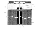
図1に本実施形態によるインクジェットヘッド用基板の基部の斜視図を、図2に図1中のA−A’断面を示す。 FIG. 1 is a perspective view of the base of the ink jet head substrate according to the present embodiment, and FIG. 2 is a cross-sectional view taken along line A-A ′ in FIG. 1.
図1に示すようにシリコン基板1(液体吐出用基板)の片側面(表面)上に、Alなどからなる配線(不図示)、TaSiN、TaNなどの高抵抗材料からなるインク吐出エネルギー発生素子2(吐出エネルギー発生部)が2列に並んで複数個形成される。そして、その上部を覆うように、SiO、SiNなどからなる絶縁保護膜3が形成される。この絶縁保護膜3は、インクやその他の液体から基板上の配線構造を守るとともに、インク供給口形成時のエッチングストップ層としての役割も担ってなる。さらに、絶縁保護膜3を形成した第1の面と逆側の第2の面(裏面)に保護膜4が形成される。保護膜4としては、基板上に少なくとも1層以上形成し、異方性エッチング液に耐性のあるものであれば何でも良い。例えば、SiOなどの絶縁膜、Mo、Au、TiN/Tiなどの金属膜、無機膜、有機膜のいずれか1層、または、2層以上の組み合わせでも良い。熱酸化膜SiOを用いれば、表面の絶縁保護膜3と同時に形成することができるが、それに限らなくても良い。
As shown in FIG. 1, on one side (surface) of a silicon substrate 1 (liquid ejection substrate), a wiring (not shown) made of Al or the like, an ink ejection energy generating element 2 made of a high resistance material such as TaSiN or TaN. A plurality of (discharge energy generating portions) are formed in two rows. Then, an insulating protective film 3 made of SiO, SiN or the like is formed so as to cover the upper part. The insulating protective film 3 protects the wiring structure on the substrate from ink and other liquids, and also serves as an etching stop layer when forming the ink supply port. Further, the
シリコン基板1表面には、絶縁保護膜3を形成する前に、図2に示すように犠牲層5が設けられる。この犠牲層5は、後述する異方性エッチング工程において、インク供給口の貫通開口幅を規定するための層となる。このとき、犠牲層材料としてAlを選択すれば、インクジェットヘッドの配線積層構造を形成するときに同時に犠牲層を作製することが可能となるため効率的である。
A
絶縁保護膜3の上部には、フォトリソグラフィーを用いて有機膜層6が積層され、インク流路および吐出口部が形成される。
An
次に、図3に示すように、シリコン基板1の裏面側から第1の未貫通孔7が形成される。尚、図3(a)はシリコン基板1の縦断面図、図3(b)はシリコン基板1の裏面側を示す平面図である。この図に示すように第1の未貫通孔7はインク供給口形成部位に対し、保護膜4を貫通してシリコン基板1の内部で留まるように形成され、図1で示すところの基板短手方向に1列、長手方向に複数形成される。また、第2の未貫通孔8が、第1の未貫通孔7の列に対して相対的に外側位置に形成される。第2の未貫通孔8もまた、保護膜4を貫通してシリコン基板1の内部で留まるように形成され、図1で示すところの基板短手方向に1列以上、長手方向に複数個形成される。第2の未貫通孔8は、(100)基板1上の[001]または[110]、もしくはそれらと等位な方位に沿って形成される。
Next, as shown in FIG. 3, a
本実施形態では、第1の未貫通孔7と第2の未貫通孔8は円または楕円を下底とする円錐形状または、円柱形状で形成されている。しかし、図12〜図15に示すように、複数個並んで列をなす第1の未貫通孔7と第2の未貫通孔8は、そのうちの一部または全てが、トレンチ形状であっても良い。
In the present embodiment, the
第1の未貫通孔7と第2の未貫通孔8の形成には、レーザ光を用いる。保護膜4の上から、未貫通孔の形成部位にレーザ光を照射すると、保護膜4およびシリコンが除去され、レーザスポットとほぼ同じ径を有する孔が形成される。第1の未貫通孔7と第2の未貫通孔8の加工深さは、レーザ種、レーザ出力条件、レーザスポット径、加工穴径およびパルス数によって、規定される。例えば、シリコンへの吸収率に優れるYAGレーザの3倍波をレーザ種として用い、出力条件5.5W 30kHz スポット径25μm 加工穴径25μmで加工した際、パルス数30回で530μmであった。レーザ種としては、YAGおよびYVO4レーザの基本波、2倍波、3倍波、4倍波、もしくは、その他のレーザを用いてもよい。なお、第1の未貫通孔7と第2の未貫通孔8は、同一工程で、同一のレーザ装置で一括加工することが工程の簡素化上、望ましいが、場合によっては、異なるレーザ装置を用いても良い。また、第2の未貫通孔8を第1の未貫通孔7に先駆けて形成しても良い。また、レーザスポットを渦巻状に走査させてトレパン加工を行うことで、第1の未貫通孔7と第2の未貫通孔8がレーザスポット径よりも大きな加工径を有していても良い。
Laser light is used to form the first
次に、TMAH中にシリコン基板1を浸漬し、異方性エッチングを行う。この処理では未貫通孔7,8の壁面すべてからエッチングが始まり、あるところではエッチングレートの低い(111)面を形成しながら、またあるところでは、エッチングレートの高い(001)(011)面やその他の面に沿ってエッチングが進行する。図4(a)〜(e)は、エッチングの進行過程を模式的に示したものである。図中の点線は、図3(a)のように第1の未貫通孔7と第2の未貫通孔8が形成されていた場所を示す。未貫通孔の各々の先端および根本部から(111)面が形成されると共に、シリコン基板1の厚みに対して垂直な方向にエッチングが進行し(図4(a))、所定の時間で未貫通孔の間が連通する(図4(b))。このとき、未貫通孔の先端付近では、(111)面同士が連結して凸部が形成される。同時に未貫通孔の根本部付近でも、(111)面同士が連結して凸部が形成される。この凸部は高次の面であるためエッチングレートが高く、シリコン基板1の厚み方向 [100]に向かってエッチングが進行することになる(図4(c)〜(d))。所定の時間が経過した時点で、犠牲層5の幅と同じ寸法でシリコン基板1表面が開口し、シリコン基板1を貫通するスロットが完成する(図4(e))。続いて、ウエット処理、ドライエッチング処理を順次行って、シリコン基板1裏面の保護膜4、シリコン基板1表面の絶縁保護膜3および有機膜層6の一部を除去する。これにより、図5に示すように、シリコン基板1の表面側のインク流路13およびノズル14(液体吐出口)と、裏面開口とを連通するインク供給口9が完成する。
Next, the
本実施形態によれば、第2の未貫通孔8を所定の条件で形成することにより、シリコン基板1裏面の開口寸法Kを制御することが可能となる。以下に、第2の未貫通孔の形成条件について詳述する。
According to the present embodiment, it is possible to control the opening dimension K on the back surface of the
図6は、未貫通孔の形成条件を模式的に示したものである。 FIG. 6 schematically shows the conditions for forming the non-through holes.
まず、第1の未貫通孔7のみによって形成されるエッチング形状に注目する。異方性エッチングによって、第1の未貫通孔7の根本部および先端部を起点として、エッチングレートの低い(111)面15,16が形成され、最終的に菱形のエッチング形状10(図6中に点線で図示)が完成する。この過程において、未貫通孔7の根本部では、基板1の厚みに対して垂直な方向へのエッチングは見かけ上ほとんど進行せず、基板1裏面の開口寸法が広がりにくい。
First, attention is paid to the etching shape formed only by the first
次に、第2の未貫通孔8を、第1の未貫通孔7の横に距離aで形成した場合を考える。第2の未貫通孔8の深さdが、
a×tan54.7°≦ d
なる関係を満たすとき、シリコン基板裏面から見て(111)面15よりも深い位置に第2の未貫通孔8の先端が存在することになる。このレーザ穴配置条件で異方性エッチングを行うと、図4で示したように、所定の時間で、第1の未貫通孔7によって形成されるエッチング形状と、第2の未貫通孔8によって形成されるエッチング形状とが合体し、未貫通孔間が連通することになる。したがって、第1および第2の未貫通孔7,8間の距離aおよび、第2の未貫通孔8の深さdを変えることで、シリコン基板1裏面の供給口寸法Kを設定することができる。
Next, consider a case where the second
a × tan 54.7 ° ≦ d
When the above relationship is satisfied, the tip of the second
図6の構成に対し、第2の未貫通孔8をn列(n≧2)形成した場合、シリコン基板1裏面の供給口の開口幅をより広く形成することが可能である(図7)。この場合も、上記と同様の考え方を適用できるため、図7に示すように第2の未貫通孔8の各々が、隣接する未貫通孔の(111)面11よりも深い位置に形成されていれば良い。すなわち、以下に示すとおりである。
In the case where n rows (n ≧ 2) of the second
複数の第1の未貫通孔7がなす列から外側に向かってm列目(2≦m≦n)の第2の未貫通孔8の深さをdmとし、m−1列とm列との間の距離をamとする。1列目の各第2の未貫通孔8の深さをd1とし、第1の未貫通孔7の列との間の距離をa1とする。この場合、第2の未貫通孔8は
a1×tan54.7°≦d1
am×tan54.7°≦dm
なる関係を満たすように形成すれば良い。
The depth of the second
a m × tan 54.7 ° ≦ d m
It may be formed so as to satisfy the relationship.
このように、本実施形態におけるインクジェットヘッド用基板の製造方法によれば、レーザ光の配置および出力条件を変えることによって、様々な裏面開口寸法を有する供給口9を形成することが可能となる。したがって、この製造方法によれば、気泡排出の信頼性を向上させたインクジェットヘッド用基板を、工程を短縮しつつ提供することが可能となる。
As described above, according to the method for manufacturing an ink jet head substrate in the present embodiment, it is possible to form the
(実施形態2)
本実施形態におけるインクジェットヘッド用基板の製造方法を説明する。
(Embodiment 2)
A method for manufacturing an ink jet head substrate in the present embodiment will be described.
まず、図1に示したようにシリコン基板1(液体吐出用基板)の片側面(表面)上に、Alなどからなる配線(不図示)、TaSiN、TaNなどの高抵抗材料からなるインク吐出エネルギー発生素子2(吐出エネルギー発生部)が2列に並んで複数個形成される。そして、その上部を覆うように、SiO、SiNなどからなる絶縁保護膜3が形成される。さらに、絶縁保護膜3を形成した第1の面と逆側の第2の面(裏面)に保護膜4が形成される。シリコン基板1表面には、絶縁保護膜3を形成する前に、図2に示すように犠牲層5が設けられる。絶縁保護膜3や犠牲層5の材料は実施形態1と同じである。
First, as shown in FIG. 1, on one side (front surface) of a silicon substrate 1 (liquid ejection substrate), wiring (not shown) made of Al or the like, ink ejection energy made of a high resistance material such as TaSiN or TaN. A plurality of generating elements 2 (discharge energy generating portions) are formed in two rows. Then, an insulating protective film 3 made of SiO, SiN or the like is formed so as to cover the upper part. Further, the
絶縁保護膜3の上部には、フォトリソグラフィーを用いて有機膜層6が積層され、インク流路および吐出口部が形成される。
An
次に、図8に示すように、シリコン基板1の裏面側から第1の未貫通孔7が形成される。尚、図8(a)はシリコン基板1の縦断面図、図8(b)はシリコン基板1の裏面側を示す平面図である。この図に示すように第1の未貫通孔7はインク供給口形成部位に対し、保護膜4を貫通してシリコン基板1の内部で留まるように形成され、図1で示すところの基板短手方向に2列以上形成され、長手方向に複数個形成される。また第2の未貫通孔8が、第1の未貫通孔7の列に対して相対的に外側位置に形成される。第2の未貫通孔8もまた、保護膜4を貫通してシリコン基板1の内部で留まるように形成され、図1で示すところの基板短手方向に1列以上形成され、長手方向に複数個形成される。第2の未貫通孔8は、(100)基板1上の[001]または[110]、もしくはそれらと等位な方位に沿って形成される。
Next, as shown in FIG. 8, the first
本実施形態では、第1の未貫通孔7と第2の未貫通孔8は円または楕円を下底とする円錐形状または、円柱形状で形成されている。しかし、図12〜図15に示すように、複数個並んで列をなす第1の未貫通孔7と第2の未貫通孔8は、そのうちの一部または全てが、トレンチ形状であっても良い。
In the present embodiment, the first
第1の未貫通孔7と第2の未貫通孔8の形成には、レーザ光を用いる。保護膜4の上から、未貫通孔の形成部位にレーザ光を照射すると、保護膜4およびシリコンが除去され、レーザスポットとほぼ同じ径を有する孔が形成される。第1の未貫通孔7と第2の未貫通孔8の加工深さは、レーザ種、レーザ出力条件、レーザスポット径、加工穴径およびパルス数によって、規定される。例えば、シリコンへの吸収率に優れるYAGレーザの3倍波をレーザ種として用い、出力条件5.5W 30kHz スポット径25μm 加工穴径25μmで加工した際、パルス数30回で530μmであった。レーザ種としては、YAGおよびYVO4レーザの基本波、2倍波、3倍波、4倍波、もしくは、その他のレーザを用いてもよい。なお、第1の未貫通孔7と第2の未貫通孔8は、同一工程で、同一のレーザ装置で一括加工することが工程の簡素化上、望ましいが、場合によっては、異なるレーザ装置を用いても良い。また、第2の未貫通孔8を第1の未貫通孔7に先駆けて形成しても良い。また、レーザスポットを渦巻状に走査させてトレパン加工を行うことで、第1の未貫通孔7と第2の未貫通孔8がレーザスポット径よりも大きな加工径を有していても良い。
Laser light is used to form the first
次に、TMAH中にシリコン基板を浸漬し、異方性エッチングを行う。この処理では未貫通孔の壁面すべてからエッチングが始まり、あるところではエッチングレートの低い(111)面を形成しながら、またあるところでは、エッチングレートの高い(001)、(011)面やその他の面に沿ってエッチングが進行する。図9(a)〜(e)は、エッチングの進行過程を模式的に示したものである。未貫通孔の各々の先端および根本部から(111)面が形成されると共に、シリコン基板1の厚みTに対して垂直な方向にエッチングが進行し(図9(a))、所定の時間で未貫通孔の間が連通する(図9(b))。このとき、未貫通孔の先端付近および根本部付近では、(111)面同士が連結して凸部が形成される。この凸部は高次の面であるためエッチングレートが高く、以後、基板1の厚み方向である[100]方向に向かってエッチングが進行することになる(図9(c)〜(d))。所定の時間が経過した時点で、犠牲層5の幅と同じ寸法でシリコン基板1表面が開口し、シリコン基板1を貫通するスロットが完成する(図9(e))。続いて、ウエット処理、ドライエッチング処理を順次行って、シリコン基板1裏面の保護膜4、シリコン基板1表面の絶縁保護膜3および有機膜層6の一部を除去する。これにより、図5に示されるように、シリコン基板1表面側のインク流路13およびノズル14(液体吐出口)と、シリコン基板1裏面の開口とを連通するインク供給口9が完成する。
Next, the silicon substrate is immersed in TMAH and anisotropic etching is performed. In this process, etching starts from all the wall surfaces of the non-through holes, and at some points, the (111) surface having a low etching rate is formed, and at other points, the (001), (011) surface having a high etching rate and other Etching proceeds along the surface. FIGS. 9A to 9E schematically show the progress of etching. A (111) plane is formed from the tip and root of each non-through hole, and etching proceeds in a direction perpendicular to the thickness T of the silicon substrate 1 (FIG. 9A). The non-through holes communicate with each other (FIG. 9B). At this time, in the vicinity of the front end and the root portion of the non-through hole, the (111) planes are connected to form a convex portion. Since this convex portion is a high-order surface, the etching rate is high, and thereafter, etching proceeds in the [100] direction, which is the thickness direction of the substrate 1 (FIGS. 9C to 9D). . When a predetermined time elapses, the surface of the
本実施形態によれば、第2の未貫通孔8を所定の条件で形成することにより、シリコン基板裏面の開口寸法を制御することが可能となる。以下に、第2の未貫通孔8の形成条件について詳述する。
According to the present embodiment, it is possible to control the opening size of the back surface of the silicon substrate by forming the second
図10は、未貫通孔の形成条件を模式的に示したものである。第1の未貫通孔7の深さをD、第2の未貫通孔8の深さをd、隣り合う第1の未貫通孔7の列と第2の未貫通孔8の列との間の距離をaと定義する。犠牲層の幅をL、最も外側にある第1の未貫通孔7と犠牲層5の中心との距離をXとする。
FIG. 10 schematically shows the conditions for forming the non-through holes. The depth of the first
まず、第1の未貫通孔7のみによって形成されるエッチング形状に注目する。異方性エッチングによって、第1の未貫通孔7の根本部および先端部を起点として、エッチングレートの低い(111)面15および16が形成され、最終的に外側が(111)面で覆われたエッチング形状10が完成する。この過程において、未貫通孔7の根本部では、シリコン基板1の厚みTに対して垂直な方向へのエッチングは見かけ上ほとんど進行せず、シリコン基板1裏面の開口寸法が広がりにくい。
First, attention is paid to the etching shape formed only by the first
次に、第2の未貫通孔8を、第1の未貫通孔7の横に距離aで形成した場合を考える。第2の未貫通孔8の深さdが、
a×tan54.7°≦ d
なる関係を満たすとき、シリコン基板裏面から見て(111)面15よりも深い位置に第2の未貫通孔8の先端が存在することになる。このレーザ穴配置条件で異方性エッチングを行うと、図9で示したように、所定の時間で、第1の未貫通孔7によって形成されるエッチング形状と第2の未貫通孔8によって形成されるエッチング形状とが合体し、未貫通孔の間が連通することになる。したがって、第1の未貫通孔7と第2の未貫通孔8の間の距離aおよび、第2の未貫通孔8の深さdを変えることで、シリコン基板1裏面の供給口寸法Kを設定することができる。
Next, consider a case where the second
a × tan 54.7 ° ≦ d
When the above relationship is satisfied, the tip of the second
また、犠牲層5の幅Lでシリコン基板1表面が開口するためには、第1の未貫通孔7を、次の関係式の範囲で形成する必要がある。
X≧L/2の場合、
T−(X−L/2)× tan54.7°≧ D ≧T−X × tan54.7°
X<L/2の場合、
T>D ≧T−X × tan54.7°
上記2つの式中の、右の不等式は、シリコン基板表面の犠牲層に異方性エッチングが到達するために求められる条件式であり、左の不等式は、異方性エッチングで形成されるシリコン基板表面の開口寸法が、犠牲層幅Lに収まるための条件である。
In order to open the surface of the
When X ≧ L / 2,
T- (XL / 2) × tan 54.7 ° ≧ D ≧ T−X × tan 54.7 °
If X <L / 2,
T> D ≧ TX × tan 54.7 °
Of the above two formulas, the right inequality is a conditional expression required for anisotropic etching to reach the sacrificial layer on the silicon substrate surface, and the left inequality is a silicon substrate formed by anisotropic etching. This is a condition for the surface opening size to be within the sacrificial layer width L.
さらに、異方性エッチングで形成されるシリコン基板表面の開口寸法が、犠牲層幅Lに収まるためには、第2の未貫通孔8に対しても、次式を満たす必要がある。
a +X ≦ T/tan54.7°+L/2
d≦ T−( a +X−L/2)×tan54.7
上の2つの不等式は、それぞれ、第2の未貫通孔8の基板内での配置に関する式と、その深さに関する式である。
Furthermore, in order for the opening dimension of the silicon substrate surface formed by anisotropic etching to be within the sacrificial layer width L, it is necessary to satisfy the following equation for the second
a + X ≦ T / tan 54.7 ° + L / 2
d ≦ T− (a + XL−2) × tan 54.7
The above two inequalities are respectively an expression relating to the arrangement of the second
図10の構成に対し、第2の未貫通孔8をn列(n≧2)形成した場合、シリコン基板1裏面の供給口の開口幅をより広く形成することが可能である(図11)。この場合も、上記と同様の考え方を適用できる。ここで、複数の第1の未貫通孔7がなす列から外側に向かってm列目(2≦m≦n)の第2の未貫通孔8の深さをdmとし、m−1列とm列との間の距離をamとする。1列目の第2の未貫通孔8の列と第1の未貫通孔7の列との間の距離をa1、1列目の第2の未貫通孔8の深さをd1とし、第1の未貫通孔7の列との間の距離をa1とする。犠牲層5の幅をL、最も外側にある第1の未貫通孔7と犠牲層5の中心との距離をXとする。
When n rows (n ≧ 2) of the second
第1および第2の未貫通孔が満たすべき条件は以下に示すとおりとなる。
X≧L/2の場合、
T−(X−L/2)× tan54.7°≧ D ≧T−X × tan54.7°
X<L/2の場合、
T> D ≧T−X × tan54.7°
a1+a2+・・・am+・・・an+X ≦T/tan54.7°+L/2
a1×tan54.7°≦d1≦T−(a1+X−L/2)×tan54.7°
am×tan54.7°≦ dm≦ T−(a1+a2+・・・am+X−L/2)×tan54.7°
このように、本実施形態におけるインクジェットヘッド用基板の製造方法によれば、レーザ光の配置および出力条件を変えることによって、様々な裏面開口寸法を有する供給口9を形成することが可能となる。したがって、この製造方法によれば、気泡排出の信頼性を向上させたインクジェットヘッドを、工程を短縮しつつ提供することが可能となる。
The conditions to be satisfied by the first and second non-through holes are as follows.
When X ≧ L / 2,
T- (XL / 2) × tan 54.7 ° ≧ D ≧ T−X × tan 54.7 °
If X <L / 2,
T> D ≧ TX × tan 54.7 °
a 1 + a 2 +... a m +... a n + X ≦ T / tan 54.7 ° + L / 2
a 1 × tan 54.7 ° ≦ d 1 ≦ T− (a 1 + XL / 2) × tan 54.7 °
a m × tan54.7 ° ≦ d m ≦ T- (a 1 + a 2 + ··· a m + X-L / 2) × tan54.7 °
As described above, according to the method for manufacturing an ink jet head substrate in the present embodiment, it is possible to form the
1 シリコン基板
4 保護膜
5 犠牲層
7 第1の未貫通孔
8 第2の未貫通孔
9 インク供給口
DESCRIPTION OF
Claims (21)
前記基板の表面に保護膜を形成する工程と、該保護膜を貫通して前記基板の内部で留まる第1の未貫通孔を形成する工程と、前記保護膜を貫通して前記基板の内部で留まる第2の未貫通孔を形成する工程と、異方性エッチングにより未貫通孔の間を連通する工程と、を含み、
前記第1の未貫通孔と前記第2の未貫通孔との間の距離をa、前記第2の未貫通孔の深さをdとしたとき、
a×tan54.7°≦ d
なる関係を満たすように前記第2の未貫通孔を形成することを特徴とするインクジェットヘッド用基板の製造方法。 A method for manufacturing a substrate for an ink jet head, comprising forming an ink supply port on a substrate,
Forming a protective film on the surface of the substrate, forming a first non-through hole that penetrates the protective film and stays inside the substrate, and penetrates the protective film inside the substrate. Forming a second non-through hole that remains, and communicating between the non-through holes by anisotropic etching,
When the distance between the first non-through hole and the second non-through hole is a, and the depth of the second non-through hole is d,
a × tan 54.7 ° ≦ d
Forming the second non-through hole so as to satisfy the following relationship.
前記基板の内部で留まる第1の未貫通孔を形成する工程と、前記基板の内部で留まる第2の未貫通孔を形成する工程と、異方性エッチングにより未貫通孔の間を連通する工程と、を含み、
前記第1の未貫通孔と前記第2の未貫通孔との間の距離をa、前記第2の未貫通孔の深さをdとしたとき、
a×tan54.7°≦ d
なる関係を満たすように第2の未貫通孔を形成することを特徴とするインクジェットヘッド用基板の製造方法。 A method for manufacturing a substrate for an ink jet head, comprising forming an ink supply port on a substrate,
Forming a first non-through hole staying inside the substrate, forming a second non-through hole staying inside the substrate, and communicating between the non-through holes by anisotropic etching And including
When the distance between the first non-through hole and the second non-through hole is a, and the depth of the second non-through hole is d,
a × tan 54.7 ° ≦ d
Forming a second non-through hole so as to satisfy the relationship.
a×tan54.7°≦ d
の関係を満たすように第2の未貫通孔を形成することを特徴とする請求項1又は請求項2に記載のインクジェットヘッド用基板の製造方法。 A row formed by the plurality of first non-through holes is formed, and a row formed by the plurality of second non-through holes is formed outside the row formed by the first non-through holes. When the distance between the row of non-through holes and the row of second non-through holes is a, and the depth of the second non-through holes is d,
a × tan 54.7 ° ≦ d
The method for producing a substrate for an inkjet head according to claim 1 or 2, wherein the second non-through hole is formed so as to satisfy the above relationship.
a1×tan54.7°≦ d1
am×tan54.7°≦ dm
の関係を満たすように第2の未貫通孔を形成することを特徴とする請求項1又は2に記載のインクジェットヘッド用基板の製造方法。 One row formed by the plurality of first non-through holes is formed, and n rows (n ≧ 2) are formed by the plurality of second non-through holes outside the row formed by the first non-through holes. formed, the depth of the second blind hole of the m-th column outwardly from the columns of the first blind pores (2 ≦ m ≦ n) and d m, the m-1 column and the m column the distance between the a m, the depth of a 1, the first column of the second blind hole the distance between the first row of the second non-through hole and a column of the first blind pores When d 1
a 1 × tan 54.7 ° ≦ d 1
a m × tan 54.7 ° ≦ d m
The method for producing a substrate for an ink jet head according to claim 1, wherein the second non-through hole is formed so as to satisfy the above relationship.
異方性エッチングによって、未貫通孔の間を連通させた後、前記基板の第1の面と第2の面を連通してインク供給口を形成する工程と、
を含む、請求項1に記載のインクジェットヘッド用基板の製造方法。 On the second surface of the substrate opposite to the first surface on which the protective film is formed, a discharge energy generating unit that generates discharge energy for discharging liquid, an ink flow path, and a discharge for discharging liquid. Forming an outlet; and
Forming an ink supply port by communicating the first surface and the second surface of the substrate after communicating between the non-through holes by anisotropic etching;
The manufacturing method of the board | substrate for inkjet heads of Claim 1 containing this.
異方性エッチングによって、未貫通孔の間を連通させた後、前記基板の第1の面と第2の面を連通してインク供給口を形成する工程と、
を含む、請求項2に記載のインクジェットヘッド用基板の製造方法。 A discharge energy generating unit that generates discharge energy for discharging liquid, an ink flow path, and a liquid are discharged onto a second surface of the substrate opposite to the first surface where the non-through hole is formed. Forming a discharge port;
Forming an ink supply port by communicating the first surface and the second surface of the substrate after communicating between the non-through holes by anisotropic etching;
The manufacturing method of the board | substrate for inkjet heads of Claim 2 containing these.
X≧L/2の場合、
T−(X−L/2)× tan54.7°≧ D ≧T−X × tan54.7°
X<L/2の場合、
T> D ≧T−X × tan54.7°
なる関係式を満たすように第1の未貫通孔を形成することを特徴とし、
第2の未貫通孔が
a+X ≦ T/tan54.7°+L/2
a×tan54.7°≦ d≦ T−(a + X −L/2)×tan54.7°
なる関係式を満たすように形成されることを特徴とする請求項19に記載のインクジェットヘッド用基板の製造方法。 Two or more rows formed by the plurality of first non-through holes are formed, and a row formed by the plurality of second non-through holes outside the row of the first non-through holes located on the outermost side from the center of the sacrificial layer. Are formed in a row, the distance between the row of the first non-through holes and the row of the second non-through holes on the outermost side is a, the depth of the second non-through holes is d, When the depth of the non-through hole is D, the width of the sacrificial layer is L, the thickness of the substrate is T, and the distance between the first non-through hole located on the outermost side from the center of the sacrificial layer and the center of the sacrificial layer is X ,
When X ≧ L / 2,
T- (XL / 2) × tan 54.7 ° ≧ D ≧ T−X × tan 54.7 °
If X <L / 2,
T> D ≧ TX × tan 54.7 °
The first non-through hole is formed so as to satisfy the following relational expression:
The second non-through hole is a + X ≦ T / tan 54.7 ° + L / 2
a × tan 54.7 ° ≦ d ≦ T− (a + X−L / 2) × tan 54.7 °
20. The method of manufacturing an inkjet head substrate according to claim 19, wherein the inkjet head substrate is formed so as to satisfy the following relational expression.
X≧L/2の場合、
T−(X−L/2)× tan54.7°≧ D ≧T−X × tan54.7°
X<L/2の場合、
T> D ≧T−X × tan54.7°
なる関係式を満たすように第1の未貫通孔を形成することを特徴とし、
第2の未貫通孔が
a1+a2+・・・am+・・・an+X ≦ T/tan54.7°+L/2
a1×tan54.7°≦d1≦T−(a1+X−L/2)×tan54.7°
am×tan54.7°≦dm≦ T−(a1+a2+・・・am+X−L/2)×tan54.7°
なる関係式を満たすように形成されることを特徴とする請求項19に記載のインクジェットヘッド用基板の製造方法。 Two or more rows formed by the plurality of first non-through holes are formed, and a row formed by the plurality of second non-through holes outside the row of the first non-through holes located on the outermost side from the center of the sacrificial layer. Are formed in n rows (n ≧ 2), and the depth of the second non-through holes in the m-th row (2 ≦ m ≦ n) is defined as d from the outermost row of the first non-through holes. m , the distance between the m-1 row and the m row is a m, and the distance between the row of the second non-through hole in the first row and the row of the first non-through hole is a 1 , The depth of the second non-through hole in the first row is d 1 , the depth of the first non-through hole is D, the width of the sacrificial layer is L, the thickness of the substrate is T, and the outermost from the center of the sacrificial layer When the distance between the first non-through hole and the center of the sacrificial layer is X,
When X ≧ L / 2,
T- (XL / 2) × tan 54.7 ° ≧ D ≧ T−X × tan 54.7 °
If X <L / 2,
T> D ≧ TX × tan 54.7 °
The first non-through hole is formed so as to satisfy the following relational expression:
The second non-through hole is a 1 + a 2 +... A m +... A n + X ≦ T / tan 54.7 ° + L / 2
a 1 × tan 54.7 ° ≦ d 1 ≦ T− (a 1 + XL / 2) × tan 54.7 °
a m × tan 54.7 ° ≦ d m ≦ T− (a 1 + a 2 +... a m + XL / 2) × tan 54.7 °
20. The method of manufacturing an inkjet head substrate according to claim 19, wherein the inkjet head substrate is formed so as to satisfy the following relational expression.
Priority Applications (2)
| Application Number | Priority Date | Filing Date | Title |
|---|---|---|---|
| JP2007231352A JP5031493B2 (en) | 2007-09-06 | 2007-09-06 | Manufacturing method of substrate for inkjet head |
| US12/203,549 US8177988B2 (en) | 2007-09-06 | 2008-09-03 | Method for manufacturing liquid discharge head |
Applications Claiming Priority (1)
| Application Number | Priority Date | Filing Date | Title |
|---|---|---|---|
| JP2007231352A JP5031493B2 (en) | 2007-09-06 | 2007-09-06 | Manufacturing method of substrate for inkjet head |
Publications (2)
| Publication Number | Publication Date |
|---|---|
| JP2009061665A JP2009061665A (en) | 2009-03-26 |
| JP5031493B2 true JP5031493B2 (en) | 2012-09-19 |
Family
ID=40430736
Family Applications (1)
| Application Number | Title | Priority Date | Filing Date |
|---|---|---|---|
| JP2007231352A Active JP5031493B2 (en) | 2007-09-06 | 2007-09-06 | Manufacturing method of substrate for inkjet head |
Country Status (2)
| Country | Link |
|---|---|
| US (1) | US8177988B2 (en) |
| JP (1) | JP5031493B2 (en) |
Families Citing this family (18)
| Publication number | Priority date | Publication date | Assignee | Title |
|---|---|---|---|---|
| US7824560B2 (en) * | 2006-03-07 | 2010-11-02 | Canon Kabushiki Kaisha | Manufacturing method for ink jet recording head chip, and manufacturing method for ink jet recording head |
| JP5219439B2 (en) * | 2007-09-06 | 2013-06-26 | キヤノン株式会社 | Manufacturing method of substrate for ink jet recording head |
| JP2009061664A (en) * | 2007-09-06 | 2009-03-26 | Canon Inc | Method for manufacturing substrate for inkjet head |
| JP5031492B2 (en) * | 2007-09-06 | 2012-09-19 | キヤノン株式会社 | Inkjet head substrate manufacturing method |
| US8197705B2 (en) * | 2007-09-06 | 2012-06-12 | Canon Kabushiki Kaisha | Method of processing silicon substrate and method of manufacturing liquid discharge head |
| JP5448581B2 (en) * | 2008-06-19 | 2014-03-19 | キヤノン株式会社 | Method for manufacturing substrate for liquid discharge head and method for processing substrate |
| JP5455461B2 (en) * | 2009-06-17 | 2014-03-26 | キヤノン株式会社 | Silicon substrate processing method and liquid discharge head substrate manufacturing method |
| JP5693068B2 (en) | 2010-07-14 | 2015-04-01 | キヤノン株式会社 | Liquid discharge head and manufacturing method thereof |
| JP5701014B2 (en) * | 2010-11-05 | 2015-04-15 | キヤノン株式会社 | Method for manufacturing ejection element substrate |
| JP5762200B2 (en) | 2011-07-29 | 2015-08-12 | キヤノン株式会社 | Manufacturing method of substrate for liquid discharge head |
| JP2013059904A (en) | 2011-09-13 | 2013-04-04 | Canon Inc | Liquid recording head and method of manufacturing the same |
| JP2013230589A (en) * | 2012-04-27 | 2013-11-14 | Canon Inc | Method for manufacturing liquid ejection head |
| JP2014046665A (en) | 2012-09-04 | 2014-03-17 | Canon Inc | Method for manufacturing liquid discharge head |
| JP6066746B2 (en) * | 2013-01-28 | 2017-01-25 | キヤノン株式会社 | Method for manufacturing substrate for liquid discharge head and method for processing silicon substrate |
| JP6094239B2 (en) * | 2013-02-06 | 2017-03-15 | セイコーエプソン株式会社 | Silicon substrate processing method |
| JP6223006B2 (en) | 2013-06-12 | 2017-11-01 | キヤノン株式会社 | Liquid discharge head chip and manufacturing method thereof |
| JP2018153978A (en) | 2017-03-16 | 2018-10-04 | キヤノン株式会社 | Silicon substrate processing method and liquid discharge head manufacturing method |
| JP7166851B2 (en) | 2018-09-07 | 2022-11-08 | キヤノン株式会社 | LIQUID EJECTION HEAD AND METHOD FOR MANUFACTURING LIQUID EJECTION HEAD |
Family Cites Families (15)
| Publication number | Priority date | Publication date | Assignee | Title |
|---|---|---|---|---|
| KR100311880B1 (en) | 1996-11-11 | 2001-12-20 | 미다라이 후지오 | Method of producing a through-hole, silicon substrate having a through-hole, device using such a substrate, method of producing an ink-jet print head, and ink-jet print head |
| JP3473664B2 (en) * | 1996-12-05 | 2003-12-08 | セイコーエプソン株式会社 | Method of manufacturing flow path forming substrate for ink jet recording head |
| EP1020291A3 (en) * | 1999-01-18 | 2001-04-11 | Canon Kabushiki Kaisha | Liquid discharge head and producing method therefor |
| AU2692100A (en) * | 1999-02-25 | 2000-09-14 | Seiko Epson Corporation | Method for machining work by laser beam |
| JP3539296B2 (en) * | 1999-08-26 | 2004-07-07 | セイコーエプソン株式会社 | Inkjet head manufacturing method |
| JP2005035281A (en) | 2003-06-23 | 2005-02-10 | Canon Inc | Manufacturing method of liquid ejection head |
| JP4522086B2 (en) * | 2003-12-15 | 2010-08-11 | キヤノン株式会社 | Beam, beam manufacturing method, ink jet recording head including beam, and ink jet recording head manufacturing method |
| JP4506717B2 (en) * | 2005-07-20 | 2010-07-21 | セイコーエプソン株式会社 | Droplet discharge head and droplet discharge apparatus |
| JP4881081B2 (en) * | 2005-07-25 | 2012-02-22 | キヤノン株式会社 | Method for manufacturing liquid discharge head |
| JP4854336B2 (en) * | 2006-03-07 | 2012-01-18 | キヤノン株式会社 | Manufacturing method of substrate for inkjet head |
| JP4850637B2 (en) | 2006-09-04 | 2012-01-11 | キヤノン株式会社 | Method for manufacturing liquid discharge head and liquid discharge head |
| JP5219439B2 (en) | 2007-09-06 | 2013-06-26 | キヤノン株式会社 | Manufacturing method of substrate for ink jet recording head |
| US8197705B2 (en) | 2007-09-06 | 2012-06-12 | Canon Kabushiki Kaisha | Method of processing silicon substrate and method of manufacturing liquid discharge head |
| JP2009061664A (en) | 2007-09-06 | 2009-03-26 | Canon Inc | Method for manufacturing substrate for inkjet head |
| JP5031492B2 (en) | 2007-09-06 | 2012-09-19 | キヤノン株式会社 | Inkjet head substrate manufacturing method |
-
2007
- 2007-09-06 JP JP2007231352A patent/JP5031493B2/en active Active
-
2008
- 2008-09-03 US US12/203,549 patent/US8177988B2/en not_active Expired - Fee Related
Also Published As
| Publication number | Publication date |
|---|---|
| JP2009061665A (en) | 2009-03-26 |
| US8177988B2 (en) | 2012-05-15 |
| US20090065476A1 (en) | 2009-03-12 |
Similar Documents
| Publication | Publication Date | Title |
|---|---|---|
| JP5031493B2 (en) | Manufacturing method of substrate for inkjet head | |
| JP4854336B2 (en) | Manufacturing method of substrate for inkjet head | |
| US8114305B2 (en) | Method of manufacturing substrate for liquid discharge head | |
| JP5219439B2 (en) | Manufacturing method of substrate for ink jet recording head | |
| JP5031492B2 (en) | Inkjet head substrate manufacturing method | |
| JP4480182B2 (en) | Inkjet recording head substrate and method of manufacturing inkjet recording head | |
| JP5028112B2 (en) | Inkjet head substrate manufacturing method and inkjet head | |
| JP5455461B2 (en) | Silicon substrate processing method and liquid discharge head substrate manufacturing method | |
| JP2009061667A (en) | Silicon substrate processing method and liquid jet head manufacturing method | |
| JP5762200B2 (en) | Manufacturing method of substrate for liquid discharge head | |
| JP2004181968A (en) | Integrated ink jet print head and its manufacturing method | |
| JP5448581B2 (en) | Method for manufacturing substrate for liquid discharge head and method for processing substrate | |
| JPH07205423A (en) | Ink-jet print head | |
| JP2006137030A (en) | Liquid discharging recording head, and its manufacturing method | |
| JP4659898B2 (en) | Manufacturing method of substrate for liquid discharge head | |
| JP5020748B2 (en) | Silicon substrate processing method and liquid discharge head manufacturing method | |
| JP5701014B2 (en) | Method for manufacturing ejection element substrate | |
| US9669628B2 (en) | Liquid ejection head substrate, method of manufacturing the same, and method of processing silicon substrate | |
| JP2009039928A (en) | Liquid discharge head and method for producing the same | |
| JP2004136679A (en) | Inkjet print head and method of manufacturing the same | |
| JP2006035854A (en) | Manufacturing method for inkjet recording head, inkjet recording head, and substrate for recording head | |
| JP2008120003A (en) | Inkjet recording head and manufacturing method for substrate for the head | |
| JP2020040227A (en) | Substrate for liquid discharge head and method for manufacturing the same | |
| JP2006224592A (en) | INKJET RECORDING HEAD AND Si SUBSTRATE FOR INKJET RECORDING HEAD | |
| JP2015201590A (en) | Method of manufacturing substrate for liquid discharge head |
Legal Events
| Date | Code | Title | Description |
|---|---|---|---|
| A621 | Written request for application examination |
Free format text: JAPANESE INTERMEDIATE CODE: A621 Effective date: 20100830 |
|
| A977 | Report on retrieval |
Free format text: JAPANESE INTERMEDIATE CODE: A971007 Effective date: 20120327 |
|
| TRDD | Decision of grant or rejection written | ||
| A01 | Written decision to grant a patent or to grant a registration (utility model) |
Free format text: JAPANESE INTERMEDIATE CODE: A01 Effective date: 20120529 |
|
| A01 | Written decision to grant a patent or to grant a registration (utility model) |
Free format text: JAPANESE INTERMEDIATE CODE: A01 |
|
| A61 | First payment of annual fees (during grant procedure) |
Free format text: JAPANESE INTERMEDIATE CODE: A61 Effective date: 20120627 |
|
| R151 | Written notification of patent or utility model registration |
Ref document number: 5031493 Country of ref document: JP Free format text: JAPANESE INTERMEDIATE CODE: R151 |
|
| FPAY | Renewal fee payment (event date is renewal date of database) |
Free format text: PAYMENT UNTIL: 20150706 Year of fee payment: 3 |