JP5019174B2 - High-speed transmission connector - Google Patents
High-speed transmission connector Download PDFInfo
- Publication number
- JP5019174B2 JP5019174B2 JP2007203274A JP2007203274A JP5019174B2 JP 5019174 B2 JP5019174 B2 JP 5019174B2 JP 2007203274 A JP2007203274 A JP 2007203274A JP 2007203274 A JP2007203274 A JP 2007203274A JP 5019174 B2 JP5019174 B2 JP 5019174B2
- Authority
- JP
- Japan
- Prior art keywords
- terminal
- contact
- grounding
- blade
- speed signal
- Prior art date
- Legal status (The legal status is an assumption and is not a legal conclusion. Google has not performed a legal analysis and makes no representation as to the accuracy of the status listed.)
- Expired - Fee Related
Links
Images


Classifications
-
- H—ELECTRICITY
- H01—ELECTRIC ELEMENTS
- H01R—ELECTRICALLY-CONDUCTIVE CONNECTIONS; STRUCTURAL ASSOCIATIONS OF A PLURALITY OF MUTUALLY-INSULATED ELECTRICAL CONNECTING ELEMENTS; COUPLING DEVICES; CURRENT COLLECTORS
- H01R13/00—Details of coupling devices of the kinds covered by groups H01R12/70 or H01R24/00 - H01R33/00
- H01R13/648—Protective earth or shield arrangements on coupling devices, e.g. anti-static shielding
- H01R13/658—High frequency shielding arrangements, e.g. against EMI [Electro-Magnetic Interference] or EMP [Electro-Magnetic Pulse]
- H01R13/6581—Shield structure
- H01R13/6585—Shielding material individually surrounding or interposed between mutually spaced contacts
- H01R13/6586—Shielding material individually surrounding or interposed between mutually spaced contacts for separating multiple connector modules
- H01R13/6587—Shielding material individually surrounding or interposed between mutually spaced contacts for separating multiple connector modules for mounting on PCBs
-
- H—ELECTRICITY
- H01—ELECTRIC ELEMENTS
- H01R—ELECTRICALLY-CONDUCTIVE CONNECTIONS; STRUCTURAL ASSOCIATIONS OF A PLURALITY OF MUTUALLY-INSULATED ELECTRICAL CONNECTING ELEMENTS; COUPLING DEVICES; CURRENT COLLECTORS
- H01R12/00—Structural associations of a plurality of mutually-insulated electrical connecting elements, specially adapted for printed circuits, e.g. printed circuit boards [PCB], flat or ribbon cables, or like generally planar structures, e.g. terminal strips, terminal blocks; Coupling devices specially adapted for printed circuits, flat or ribbon cables, or like generally planar structures; Terminals specially adapted for contact with, or insertion into, printed circuits, flat or ribbon cables, or like generally planar structures
Landscapes
- Details Of Connecting Devices For Male And Female Coupling (AREA)
- Coupling Device And Connection With Printed Circuit (AREA)
Description
本発明は、高速信号伝送路の一部を形成する高速伝送用コネクタに関する。 The present invention relates to a high-speed transmission connector that forms part of a high-speed signal transmission path.
データ伝送が比較的高速で行われる場合、例えば、1チャンネルあたり2.5Gbps以上の高速信号伝送を実現するために差動伝送方式が採用されている。このような差動伝送方式が採用される伝送路において、例えば、配線基板としてのマザーボードとドーターボートとの間を電気的に接続するための高速伝送用コネクタが実用に供されている。このような高速伝送用コネクタにおいては、例えば、特許文献1にも示されるように、バックプレーンコネクタと称されるコネクタが提案されている。
When data transmission is performed at a relatively high speed, for example, a differential transmission method is employed to realize high-speed signal transmission of 2.5 Gbps or more per channel. In a transmission line employing such a differential transmission method, for example, a high-speed transmission connector for electrically connecting a mother board as a wiring board and a daughter boat is practically used. As such a high-speed transmission connector, for example, as shown in
バックプレーンコネクタは、その内側に複数個配置される接続端子(ブレード接点)により、マザーボード、および、後述するドーターカードコネクタに電気的に接続されるものとされる。ドーターボードに配置されるドーターカードコネクタは、複数枚のウェーハを互いに重ねて内側に収容するハウジングを備えている。 The backplane connector is electrically connected to a mother board and a daughter card connector (to be described later) by a plurality of connection terminals (blade contacts) arranged inside the backplane connector. A daughter card connector disposed on a daughter board includes a housing that accommodates a plurality of wafers on top of each other.
各ウェーハは、複数個の接地用端子を所定の間隔で一端部に有するドーターカードシールド部材と、複数個の信号用端子を所定の間隔で一端部に有する信号接点ブランクを支持する支持プレート(ハウジング)とから構成されている。ドーターカードシールド部材と信号接点ブランクとは、一対の接地用端子および信号用端子が一列状に配され、かつ、
一対の接地用端子の相互間に一対の信号用端子とが、配置されるように互いに重ねられている。
Each wafer has a daughter card shield member having a plurality of ground terminals at one end at a predetermined interval and a support plate (housing) supporting a signal contact blank having a plurality of signal terminals at one end at a predetermined interval. ). The daughter card shield member and the signal contact blank have a pair of grounding terminals and signal terminals arranged in a line, and
A pair of signal terminals are overlapped with each other so as to be disposed between the pair of ground terminals.
信号接点ブランクにおいて、各信号ラインを形成する伝送路の両端にそれぞれ、ドーターボード用端子部(接点テイル)と、伝送路の幅に比して大なる幅を有するブレード接点用端子部(連続接点領域)とが形成されている。 In the signal contact blank, the daughter board terminal part (contact tail) and the blade contact terminal part (continuous contact) having a width larger than the width of the transmission line at both ends of the transmission line forming each signal line, respectively. Region).
上述のような高速伝送路においては、例えば、信号の反射の原因となるコネクタ内部におけるインピーダンス不整合も無視することができないので上述のバックプレーンコネクタの内部におけるインピーダンス整合も要望される。また、隣接する伝送路間のクロストークを防止することも必要とされる。 In the above-described high-speed transmission path, for example, impedance mismatching inside the connector that causes signal reflection cannot be ignored, so that impedance matching inside the backplane connector is also desired. It is also necessary to prevent crosstalk between adjacent transmission lines.
しかしながら、上述したように、ブレード接点用端子部は、その伝送路の幅に比して大なる幅を有するのでインピーダンスが変化する虞があり、従って、インピーダンス整合が取り難いという問題を伴う。このようにインピーダンス整合が取り難い場合、信号反射の原因となるので近年要望されている1チャンネルあたり10Gbps以上のさらなる高速信号伝送を実現することが困難となる。 However, as described above, since the blade contact terminal portion has a width that is larger than the width of the transmission path, there is a possibility that the impedance may change, and therefore, there is a problem that it is difficult to achieve impedance matching. When impedance matching is difficult to achieve in this way, it becomes a cause of signal reflection, and it becomes difficult to realize further high-speed signal transmission of 10 Gbps or more per channel, which has been requested in recent years.
また、信号接点ブランクにおける連続接点領域においては、シールドプレートに一体に形成されるシールドビーム接点は、ビーム接点対相互間に配置される。しかし、シールドビーム接点のビーム接点に対する位置決めが確実でない構成を有しているので隣接する伝送路間のクロストークの防止に関しては不十分となる虞がある。 In the continuous contact region in the signal contact blank, the shield beam contact formed integrally with the shield plate is disposed between the beam contact pairs. However, since the shield beam contact is not reliably positioned with respect to the beam contact, there is a risk that the prevention of crosstalk between adjacent transmission paths may be insufficient.
以上の問題点を考慮し、本発明は、高速伝送用コネクタであって、隣接する伝送路間のクロストークを確実に防止し、かつ、コネクタ内部のインピーダンス整合を容易に行なうことができる高速伝送用コネクタを提供することを目的とする。 In view of the above problems, the present invention is a high-speed transmission connector that reliably prevents crosstalk between adjacent transmission lines and can easily perform impedance matching inside the connector. An object is to provide a connector.
上述の目的を達成するために、本発明に係る高速伝送用コネクタは、共通の平面上において隣接する二つの高速信号用伝送路の接続端を挟んで配される二つの接地用端子部を複数個有する接地用ブレードを含んでなるコンタクトユニットと、コンタクトユニットを着脱可能に収容するケーシングを有するプラグ部と、プラグ部に接続される場合、コンタクトユニットの二つの高速信号用伝送路の接続端にそれぞれ接続される高速信号用伝送路と、高速信号用伝送路の両脇にそれぞれ伝送路を挟むように配され、接地用ブレードの接地用端子部にそれぞれ、接続される接地用端子と有するソケット部と、を備え、二つの接地用端子部は、接地用コンタクト端子の先端部に二つに分岐して形成され、二つの高速信号用伝送路の接続端がそれぞれ、接地用端子部相互間に形成され、二つの接地用端子部は、薄板状の接地用コンタクト端子の先端部で厚さ方向に沿って互いに逆方向に折り曲げられ、斜めに相対向することを特徴とする。
また、本発明に係る高速伝送用コネクタは、共通の平面上において隣接する二つの高速信号用伝送路の接続端を挟んで共通の平面上に配される二つの接地用端子部を有する接地用ブレードを含んでなるコンタクトユニットと、コンタクトユニットを着脱可能に収容するケーシングを有するプラグ部と、プラグ部に接続される場合、コンタクトユニットの二つの高速信号用伝送路の接続端にそれぞれ接続される高速信号用伝送路と、高速信号用伝送路の両脇にそれぞれ伝送路を挟むように配され、接地用ブレードの接地用端子部にそれぞれ、接続される接地用端子と有するソケット部と、を備え、二つの高速信号用伝送路の全長における線路長差が、0.5mmであることを特徴とする。
さらに、本発明に係る高速伝送用コネクタは、共通の平面上において隣接する二つの高速信号用伝送路の接続端を挟んで共通の平面上に配される二つの接地用端子部を有する接地用ブレードを含んでなるコンタクトユニットと、コンタクトユニットを着脱可能に収容するケーシングを有するプラグ部と、プラグ部に接続される場合、コンタクトユニットの二つの高速信号用伝送路の接続端にそれぞれ接続される高速信号用伝送路と、高速信号用伝送路の両脇にそれぞれ伝送路を挟むように配され、接地用ブレードの接地用端子部にそれぞれ、接続される接地用端子と有するソケット部と、を備え、二つの接地用端子部は、接地用コンタクト端子の先端部に二つに分岐して形成され、二つの高速信号用伝送路の接続端がそれぞれ、接地用端子部相互間に形成され、隣接する二つの高速信号用伝送路を有し、コンタクトユニットの一部を構成する伝送用ブレードの表面と接地用コンタクト端子の表面との間に所定の空間が形成され、二つの高速信号用伝送路にそれぞれ、個別に連結され、配線基板の導体に当接する端子部を有し、端子部を配線基板の導体に向けて付勢する湾曲部が、互いに異なる曲率半径を有し、伝送用ブレードにおける共通の平面上に所定の間隔をもって一列に配列されることを特徴とする。
To achieve the above object, a high speed transmission connector according to the present invention, a plurality of two grounding terminal portion distribution across the connection end of the two high-speed signal transmission lines adjacent to each other in a common plane A contact unit including a grounding blade, a plug unit having a casing for detachably accommodating the contact unit, and, when connected to the plug unit, at the connection end of the two high-speed signal transmission lines of the contact unit A high-speed signal transmission line to be connected to each other, and a socket having a grounding terminal to be connected to each of the grounding terminal portions of the grounding blade, with the transmission line being sandwiched on both sides of the high-speed signal transmission line. comprising a part, the two ground terminal portion is formed by branching into two at the tip of the ground contact terminal, the connection end of the transmission path for the two high-speed signals, respectively, It is formed between the ground terminal parts, and the two grounding terminal parts are bent in opposite directions along the thickness direction at the front end part of the thin plate-like grounding contact terminal, and face each other diagonally. And
The high-speed transmission connector according to the present invention includes a grounding terminal having two grounding terminal portions arranged on a common plane across the connection ends of two adjacent high-speed signal transmission paths on a common plane. A contact unit including a blade, a plug portion having a casing that detachably accommodates the contact unit, and, when connected to the plug portion, are connected to connection ends of two high-speed signal transmission paths of the contact unit, respectively. A high-speed signal transmission line, and a socket part having a ground terminal connected to the grounding terminal part of the grounding blade, which is arranged so as to sandwich the transmission line on both sides of the high-speed signal transmission line, respectively. The line length difference in the entire length of the two high-speed signal transmission lines is 0.5 mm .
Further, the high-speed transmission connector according to the present invention has two grounding terminal portions arranged on a common plane across the connection ends of two adjacent high-speed signal transmission lines on the common plane. A contact unit including a blade, a plug portion having a casing that detachably accommodates the contact unit, and, when connected to the plug portion, are connected to connection ends of two high-speed signal transmission paths of the contact unit, respectively. A high-speed signal transmission line, and a socket part having a ground terminal connected to the grounding terminal part of the grounding blade, which is arranged so as to sandwich the transmission line on both sides of the high-speed signal transmission line, respectively. The two grounding terminal portions are formed by branching into two at the tip of the grounding contact terminal, and the connection ends of the two high-speed signal transmission paths are respectively grounding terminal portions. A predetermined space is formed between the surface of the transmission blade and the surface of the contact terminal for grounding, which are formed between each other and have two adjacent high-speed signal transmission lines, and constitute a part of the contact unit, Each of the two high-speed signal transmission paths is individually connected and has a terminal portion that contacts the conductor of the wiring board, and the curved portion that biases the terminal portion toward the conductor of the wiring board has different radii of curvature. The transmission blades are arranged in a line at a predetermined interval on a common plane in the transmission blade.
以上の説明から明らかなように、本発明に係る高速伝送用コネクタによれば、コンタクトユニットは、共通の平面上において隣接する二つの高速信号用伝送路の接続端を挟んで共通の平面上に配される二つの接地用端子部を有する接地用ブレードを含んでなるので隣接する伝送路間のクロストークを確実に防止し、かつ、コネクタ内部のインピーダンス整合を容易に行なうことができる。 As is clear from the above description, according to the high-speed transmission connector according to the present invention, the contact unit is on a common plane across the connection ends of two adjacent high-speed signal transmission paths on a common plane. Since the grounding blade having two grounding terminal portions arranged is included, crosstalk between adjacent transmission paths can be reliably prevented, and impedance matching inside the connector can be easily performed.
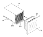
図2は、本発明に係る高速伝送用コネクタの一例の外観を、プリント配線板とともに示す。 FIG. 2 shows the appearance of an example of a high-speed transmission connector according to the present invention together with a printed wiring board.
図2において、高速伝送用コネクタは、所定のプリント配線板12に固定されるプラグ部10と、所定のプリント配線板16に固定されるソケット部14とを含んで構成されている。なお、図2は、プラグ部10がソケット部14に接続されている状態を示す。
In FIG. 2, the high-speed transmission connector includes a
プラグ部10は、図3に示されるように、ソケット部14に対し着脱可能とされる構成を備えている。プラグ部10は、図4乃至図6、および、図8に示されるように、後述する各ブレード型コンタクトユニット18Bi(i=1〜n,nは正の整数)を着脱可能に収容する複数のセル10Si(i=1〜n,nは正の整数)を有するケーシング10Cを備えて構成される。
As shown in FIG. 3, the
樹脂材料、例えば、液晶ポリマー(LCP)で成形されるケーシング10Cは、図5に示されるように、プリント配線板12が配される段差部10Dを底部に有している。段差部10Dには、図7に拡大されて示されるように、セル10Siに連通する開口部が所定の間隔で形成されている。各開口部には、後述する各ブレード型コンタクトユニット18Biの接地用端子および信号用端子が露出している。各開口部相互間は、セル10Si相互間を仕切る隔壁10Wiに連なり形成される隔壁により区切られている。
As shown in FIG. 5, the
ケーシング10Cにおけるセル10Siは、図8に示されるように、その長辺に対し略平行に所定の間隔で形成されている。各セル10Siは、ケーシング10Cの内側にその長辺に沿って延在している。各セル10Siにおける底部側には、図8に示される矢印の示す方向に沿ってコンタクトユニット18Biが着脱される場合、コンタクトユニット18Biの接地用端子および信号用端子側の端部を案内する案内溝が形成されている。隣接するセル10Si相互間は、隔壁10Wiにより区切られている。
As shown in FIG. 8, the
ケーシング10Cにおける両側壁には、それぞれ、図4に示されるように、後述するソケット部14における両端に位置する接続端部が係合される凹部10Rが形成されている。プラグ部10が後述するソケット部14に接続される場合、ケーシング10Cにおけるセル10Siの開口端面は、後述するソケット部14における段差面50S(図24参照)に当接するものとされる。
As shown in FIG. 4, the both side walls of the
一枚のコンタクトユニット18Biは、図1に拡大されて示されるように、一枚の接地用ブレード24と、接地用ブレード24における相対向する外面にそれぞれ配される2枚の伝送用ブレード26とを含んで構成される。接地用ブレード24は、後述する接地用コンタクト端子群22G1〜22G6、22’G1〜22’G6(図10参照)を含んで構成されている。また、伝送用ブレード26は、信号またはデータを伝送する伝送用コンタクト端子群30a〜30mを含んで構成されている。
As shown in an enlarged view in FIG. 1, one contact unit 18 </ b> Bi includes one
接地用ブレード24は、図10に拡大されて示されるように、2枚の支持プレート20と、各支持プレート20の溝に挿入される接地用コンタクト端子群22G1〜22G6、22’G1〜22’G6とを含んで構成されている。
As shown in an enlarged view in FIG. 10, the
各支持プレート20は、例えば、電気的絶縁性材料としての樹脂材料である液晶ポリマー(LCP)で成形されており、互いに同一の構造を有するので一方の支持プレート20について説明し、他方の支持プレート20についての説明を省略する。
Each
支持プレート20は、その下端部に上述のプリント配線板12の一方の端部に係合される段差部20Sを有している。
The
支持プレート20の一方の表層部には、薄板状の各接地用コンタクト端子がそれぞれ、個別に挿入される溝20Ga〜20Gfが形成されている。
In one surface layer portion of the
上述の段差部20Sに最も近い位置に形成されている溝20Gfには、接地用コンタクト端子22G6が挿入されている。溝20Gfの一方の端部は、二股状に分岐している。一方、溝20Gfの他方の端部は、段差部20Sに隣接して内側に略平行に形成される合流溝Gcoに連通している。なお、合流溝Gcoは、溝20Ga〜20Gfの他方の端部に共通して連通するように溝20Ga〜20Gfの深さと等しい深さで形成されている。合流溝Gcoには、接地用コンタクト端子群22G1〜22G6の各固定端子部が一列に挿入される。
A ground contact terminal 22G6 is inserted into the groove 20Gf formed at a position closest to the above-described
溝20Gfにおける一方の端部と他方の端部との間の部分は、折れ曲がっている。その折曲部は、高低差のある二つの水平な部分を傾斜部分で連結するように形成されている。 A portion between one end and the other end of the groove 20Gf is bent. The bent portion is formed so as to connect two horizontal portions having different heights with an inclined portion.
溝20Gfおよび他の溝20Ge〜20Gaの深さは、図15に部分的に拡大して示されるように、後述する接地用コンタクト端子22G1〜22G6の厚さよりも大に設定されている。これにより、図14および図15に示されるように、段差Deが、支持プレート20の外表面と挿入された接地用コンタクト端子22G1〜22G6の表面との間に形成されることとなる。
The depths of the grooves 20Gf and the other grooves 20Ge to 20Ga are set larger than the thickness of ground contact terminals 22G1 to 22G6 described later, as partially enlarged in FIG. Thereby, as shown in FIG. 14 and FIG. 15, the step De is formed between the outer surface of the
従って、後述する伝送用ブレード26が支持プレート20に重ね合わされる場合、図16(A)に部分的に拡大されて示されるように、接地用コンタクト端子22G1〜22G6の表面と相対向する伝送用ブレード26の表面との間に、段差Deに対応した所定の空気層AGが形成されることとなる。
Accordingly, when a
溝20Gfよりも上方の位置にある溝20Ge〜20Gaには、それぞれ、接地用コンタクト端子22G5、22G4、22G3,22G2,22G1が挿入されている。 Grounding contact terminals 22G5, 22G4, 22G3, 22G2, and 22G1 are inserted into the grooves 20Ge to 20Ga located above the groove 20Gf, respectively.
溝20Gfに隣接する溝20Geの形状は、所定の間隔をもって溝20Gfの形状と相似形に形成されている。溝20Geは、溝20Gfを囲うように形成されている。 The shape of the groove 20Ge adjacent to the groove 20Gf is similar to the shape of the groove 20Gf with a predetermined interval. The groove 20Ge is formed so as to surround the groove 20Gf.
溝20Geに隣接する溝20Gdの形状は、所定の間隔をもって溝20Gfの形状と相似形に形成されている。溝20Gdは、溝20Geを囲うように形成されている。 The shape of the groove 20Gd adjacent to the groove 20Ge is similar to the shape of the groove 20Gf with a predetermined interval. The groove 20Gd is formed so as to surround the groove 20Ge.
溝20Gdに隣接する溝20Gcの形状は、所定の間隔をもって溝20Gfの形状と相似形に形成されている。溝20Gcは、溝20Gdを囲うように形成されている。 The shape of the groove 20Gc adjacent to the groove 20Gd is similar to the shape of the groove 20Gf with a predetermined interval. The groove 20Gc is formed so as to surround the groove 20Gd.
溝20Gcに隣接する溝20Gbの形状は、所定の間隔をもって溝20Gfの形状と相似形に形成されている。溝20Gbは、溝20Gcを囲うように形成されている。 The shape of the groove 20Gb adjacent to the groove 20Gc is similar to the shape of the groove 20Gf with a predetermined interval. The groove 20Gb is formed so as to surround the groove 20Gc.
溝20Gbに隣接する溝20Gaの形状は、所定の間隔をもって溝20Gfの形状と相似形に形成されている。溝20Gaは、溝20Gbを囲うように形成されている。 The shape of the groove 20Ga adjacent to the groove 20Gb is similar to the shape of the groove 20Gf with a predetermined interval. The groove 20Ga is formed so as to surround the groove 20Gb.
これにより、支持プレート20の一方の端部には、二つに分岐した溝が所定の間隔をもって一列状に形成されることとなる。
As a result, two branched grooves are formed in one row at a predetermined interval at one end of the
接地用コンタクト端子群22G1〜22G6と、接地用コンタクト端子群22’G1〜22’G6とは、それぞれ、その固定端子部22gt、22gt’の位置の相違を除き、互いに同一形状とされるので接地用コンタクト端子群22G1〜22G6について説明し、接地用コンタクト端子群22’G1〜22’G6の説明を省略する。
The grounding contact terminal groups 22G1 to 22G6 and the grounding
接地用コンタクト端子22G6は、銅合金材料、例えば、リン青銅合金材料で薄板状に作られている。接地用コンタクト端子22G6の一方の端部は、図11に部分的に拡大して示されるように、二股状に分岐している一対の端子22Gcを有している。接地用コンタクト端子22G6の中間部分に対し外方へ離隔するように折り曲げられた一対の端子22Gcは、所定の間隔をもって互いに平行に、かつ、固定される支持プレート20の短辺に直交するように延びている。一対の端子22Gc(グランドパッド部)は、上下に隣接する信号とのクロストーク防止の為に上下に二つのパッドとして分けられている。
The ground contact terminal 22G6 is made of a copper alloy material, for example, a phosphor bronze alloy material in a thin plate shape. One end portion of the ground contact terminal 22G6 has a pair of terminals 22Gc branched in a bifurcated manner, as partially enlarged in FIG. The pair of terminals 22Gc bent so as to be separated outward from the intermediate portion of the ground contact terminal 22G6 are parallel to each other at a predetermined interval and orthogonal to the short side of the
一方、接地用コンタクト端子22G6の他方の端部には、図11に拡大されて示されるように、後述するプリント配線板12のスルーホールに圧入される固定端子部22gtを有する平坦な拡張部22Gaが形成されている。固定端子部22gtは、上述の端子22Gcの延長線に対し略直交するように拡張部22Gaの端部に形成されている。接地用コンタクト端子22G6における一方の端部と他方の端部との間の部分22Gbは、折れ曲がっている。その折曲部は、高低差のある二つの水平な部分を傾斜部分で連結するように形成されている。
On the other hand, at the other end of the ground contact terminal 22G6, as shown in an enlarged view in FIG. 11, a flat extension portion 22Ga having a fixed terminal portion 22gt press-fitted into a through hole of the printed
接地用コンタクト端子22G6に隣接して上方に配される接地用コンタクト端子22G5、および、さらにその上方に配される他の接地用コンタクト端子22G4〜22G1の形状は、接地用コンタクト端子22G6の形状に対し互いに相似形とされる。 The ground contact terminal 22G5 disposed above and adjacent to the ground contact terminal 22G6, and the other ground contact terminals 22G4 to 22G1 disposed above the ground contact terminal 22G6 have the same shape as the ground contact terminal 22G6. On the other hand, they are similar to each other.
接地用コンタクト端子22G1〜22G6の線路長に関しては、接地用コンタクト端子22G6の線路長が最小値に設定され、接地用コンタクト端子22G1の線路長が最大値に設定されている。接地用コンタクト端子22G5の線路長は、接地用コンタクト端子22G6の線路長よりも大に設定されており、また、接地用コンタクト端子22G4の線路長は、接地用コンタクト端子22G5の線路長よりも大に設定され、さらに、接地用コンタクト端子22G3の線路長は、接地用コンタクト端子22G4の線路長よりも大に設定されている。そして、接地用コンタクト端子22G2の線路長は、接地用コンタクト端子22G3の線路長よりも大に設定されている。これにより、図11に示されるように、接地用コンタクト端子22G1〜22G6の線路長の短い順序で共通の平面上に配列される場合、相対的に線路長が短い接地用コンタクト端子は、相対的に線路長が長い接地用コンタクト端子により囲まれることとなる。 Regarding the line length of the ground contact terminals 22G1 to 22G6, the line length of the ground contact terminal 22G6 is set to the minimum value, and the line length of the ground contact terminal 22G1 is set to the maximum value. The line length of the ground contact terminal 22G5 is set larger than the line length of the ground contact terminal 22G6, and the line length of the ground contact terminal 22G4 is larger than the line length of the ground contact terminal 22G5. Further, the line length of the ground contact terminal 22G3 is set larger than the line length of the ground contact terminal 22G4. The line length of the ground contact terminal 22G2 is set larger than the line length of the ground contact terminal 22G3. Accordingly, as shown in FIG. 11, when the ground contact terminals 22G1 to 22G6 are arranged on a common plane in a short order of the line length, the ground contact terminals having a relatively short line length are relatively Is surrounded by a ground contact terminal having a long line length.
また、接地用コンタクト端子22G1〜22G6、および、22’G1〜22’G6が、それぞれ、共通の接合面で接合された各支持プレート20の各溝20Ga〜20Gfに挿入された場合、図11に示されるように、例えば、接地用コンタクト端子22G1と接地用コンタクト端子22’G1とが向かい合うように配置されることとなる。その際、図12に示されるように、その固定端子部22gtの位置は、固定端子部22gt’の位置に比して所定距離、支持プレート20の前端に近くなるように設定されている。
Further, when the ground contact terminals 22G1 to 22G6 and 22′G1 to 22′G6 are respectively inserted into the grooves 20Ga to 20Gf of the
接地用コンタクト端子22G1〜22G6、および、22’G1〜22’G6が上述のように一体化された接地用ブレード24は、例えば、約0.7mmの厚さで比較的薄く成形されているので柔軟性を有している。
The
伝送用ブレード26は、図17に拡大されて示されるように、例えば、各伝送路をそれぞれ、形成するコンタクト端子群30a〜30mを所定の間隔をもって配置した状態で電気的絶縁材料としての樹脂材料である液晶ポリマーでインサート成形された構造を有している。樹脂製の伝送用ブレード26の基材26Bは、例えば、厚さ約0.4mmに設定されているので柔軟性を有している。伝送用ブレード26は、接地用ブレード24における相対向する外面にそれぞれ、後述のコンタクトパッド形成部を介して固定された状態で配置される。
As shown in FIG. 17 in an enlarged manner, the
伝送用ブレード26の一方の端部には、上述の接地用ブレード24における一対の端子22Gcの相互間にそれぞれ配される複数のコンタクトパッド形成部26Bpが所定の間隔で形成されている。隣接するコンタクトパッド形成部26Bp相互間には、切欠部26Bcが形成されている。また、伝送用ブレード26の基材26Bの最下端部には、上述のプリント配線板12の端部に係合される段差部26Baが、接地用ブレード24における支持プレート20の段差部20Sに向き合って同一の形状に形成されている。
At one end portion of the
コンタクト端子群30a〜30mは、例えば、リン青銅合金材料で薄板状に作られ、図18に拡大されて示されるように、互いに線路長が異なるものとされる。コンタクト端子30aの線路長が最大長さに設定され、また、コンタクト端子30mの線路長が最小長さに設定されている。コンタクト端子30aおよび30b、30cおよび30d、30eおよび30f、30gおよび30h、30iおよび30j、30kおよび30mは、それぞれ、一対の信号路を形成するものとされる。
The
コンタクト端子群30a〜30mのうちコンタクト端子30aは、基材26Bの最上端部近傍の位置に配され、一方、コンタクト端子30mは、基材26Bの最下端部の段差部26Ba近傍の位置に配される。
Of the
コンタクト端子30mの一方の端部は、図19に部分的に拡大して示されるように、コンタクトパッド30cpを有している。コンタクトパッド30cpにおけるその配列方向に沿った幅は、他の部分の幅に比して大に設定されている。
One end of the
一方、コンタクト端子30mの他方の端部には、後述するプリント配線板12の導体パターンに所定の圧力で当接される端子部30tを有する湾曲部30bnが形成されている。端子部30tは、上述のコンタクトパッド30cpの延長線に対し略直交するように弾性を有する湾曲部30bnの端部に形成されている。コンタクト端子30mにおける一方の端部と他方の湾曲部との間の部分は、図12にニ点鎖線で示されるように、上述の接地用コンタクト端子22G6の部分22Gbに対向しつつ、基材26Bの表面上で折れ曲がっている。その折曲部は、高低差のある二つの水平な部分を傾斜部分で連結するように形成されている。
On the other hand, a curved portion 30bn having a
コンタクト端子30mに隣接して上方に配されるコンタクト端子30k、および、さらにその上方に配される他のコンタクト端子30j〜30aの形状は、コンタクト端子30mの形状に対し互いに相似形とされる。
The
コンタクト端子30a〜30mにおけるコンタクトパッド30cpと湾曲部との間の線路長(以下、実効線路長ともいう)に関しては、差動伝送方式においては、一対の信号路相互間の線路長を同一長さにすることが望ましい。
Regarding the line length between the contact pad 30cp and the curved portion (hereinafter also referred to as effective line length) in the
本実施例においては、図20および図21に示されるように、一対の信号路PL1を形成するコンタクト端子30a,30bの実効線路長(mm)は、それぞれ、例えば、38.1,36.17に設定されているのでコンタクト端子30bは、線路長差ΔLとして1.23mmだけ短くなる。一対の信号路PL2を形成するコンタクト端子30c,30dの実効線路長は、それぞれ、例えば、32.19,30.94に設定されているのでコンタクト端子30dは、線路長差ΔLとして1.25mmだけ短くなる。一対の信号路PL3を形成するコンタクト端子30e,30fの実効線路長は、それぞれ、例えば、26.26,25.02に設定されているのでコンタクト端子30fは、線路長差ΔLとして1.24mmだけ短くなる。一対の信号路PL4を形成するコンタクト端子30g,30hの実効線路長は、それぞれ、例えば、21.09,19.84に設定されているのでコンタクト端子30hは、線路長差ΔLとして1.25mmだけ短くなる。
In this embodiment, as shown in FIGS. 20 and 21, the effective line lengths (mm) of the
一対の信号路PL5を形成するコンタクト端子30i,30jの実効線路長は、それぞれ、例えば、15.95,14.71に設定されているのでコンタクト端子30jは、線路長差ΔLとして1.24mmだけ短くなる。一対の信号路PL6を形成するコンタクト端子30k,30mの実効線路長は、それぞれ、例えば、10.81,9.57に設定されているのでコンタクト端子30mは、線路長差ΔLとして1.24mmだけ短くなる。
The effective line lengths of the contact terminals 30i and 30j forming the pair of signal paths PL5 are set to, for example, 15.95 and 14.71, respectively. Therefore, the contact terminal 30j has a line length difference ΔL of 1.24 mm. Shorter. Since the effective line lengths of the
上述の各信号路PL1〜PL6の線路長差ΔLは、後述するように、各信号路PL1〜PL6のうちより短い信号路を形成するコンタクト端子の端部を、湾曲部30bnにおける線路長のより長い部分と一体にすることにより、その全長における線路長差が更に約0.5mm程度小さくなる。 As described later, the line length difference ΔL of each of the signal paths PL1 to PL6 corresponds to the end of the contact terminal that forms a shorter signal path among the signal paths PL1 to PL6 by the line length of the curved portion 30bn. By integrating with the long part, the line length difference in the entire length is further reduced by about 0.5 mm.
その際、図17に示されるように、コンタクト端子30a〜30mの線路長の短い順序で共通の平面上に配列される場合、相対的に線路長が短いコンタクト端子は、相対的に線路長が長いコンタクト端子により囲まれることとなる。また、コンタクト端子の配列方向に沿ってコンタクト端子の湾曲部を所定の間隔で並べることで、ブレード毎の端子部30tが干渉することなく並べることが出来ることとなる。
In this case, as shown in FIG. 17, when the
上述の例においては、伝送用ブレード26の基材26Bにおけるコンタクトパッド形成部26Bpの先端部は、図1に示されるように、支持プレート20の端部を貫通することなく、その段差部で位置規制されているが、斯かる例に限られることなく、例えば、図22(A)に部分的に拡大されて示されるように、伝送用ブレード38の基材38Bにおけるコンタクトパッド形成部38Bpの先端部が支持プレートの端部32における端子22Gc相互間に形成される溝32Dに嵌合されるものでもよい。なお、図22(A)〜(D)においては、コンタクト端子30a〜30mの配列は、図17に示される例と同一とされる。
In the above example, the tip of the contact pad forming portion 26Bp in the
また、例えば、図22(B)に部分的に拡大されて示されるように、伝送用ブレード40の基材40Bにおけるコンタクトパッド形成部40Bpの先端部が支持プレートの端部34における端子22Gc相互間に形成される溝34Dに嵌合された状態で、コンタクトパッド形成部40Bpにおけるコンタクトパッド30cp相互間、および、端子22Gc相互間に溝40AGが、コンタクトパッド30cpの厚さと同一の深さで形成されてもよい。これにより、例えば、インピーダンス調整において、コンタクトパッドの保持強度を維持しつつ、インピーダンスを増大させることが可能となる。
Also, for example, as shown in a partially enlarged view in FIG. 22B, the tip of the contact pad forming portion 40Bp in the base material 40B of the
さらに、例えば、図22(C)に部分的に拡大されて示されるように、伝送用ブレード42の基材42Bにおけるコンタクトパッド形成部42Bpの先端部が支持プレートの端部36における端子22Gc相互間に形成される溝36Dに嵌合された状態で、コンタクトパッド形成部42Bpにおけるコンタクトパッド30cp相互間、および、端子22Gc相互間に溝42G1、42G2、および、42G3が、コンタクトパッド30cpの厚さよりも大なる深さで形成されてもよい。これにより、例えば、インピーダンス調整において、インピーダンスを増大させることが可能となる。
Further, for example, as shown in a partially enlarged view in FIG. 22C, the tip of the contact pad forming portion 42Bp in the base material 42B of the
そして、図22(B)に示される例において、例えば、図22(D)に部分的に拡大されて示されるように、コンタクト端子30k’、30m’において、それぞれ、コンタクトパッド30cp近傍における上流側部分に、縮小部30Eが、例えば、幅0.2mm,長さ1.0mm程度形成されてもよい。
In the example shown in FIG. 22 (B), for example, as shown partially enlarged in FIG. 22 (D), the
さらにまた、図16(B)に部分的に拡大されて示されるように、伝送用ブレード26におけるコンタクト端子30a〜30mが埋設される部分に近接する表面にも、凹部が形成されてもよい。これにより、コンタクトユニット18Biがセル18Siに装着される場合、ケーシング10Cの隔壁10Wiの表面と伝送用ブレード26のコンタクト端子30a〜30mがそれぞれ、埋設される部分に近接する表面との間に、空気層を形成する隙間AGSが形成されることとなる。
Furthermore, as shown in a partially enlarged view in FIG. 16B, a recess may be formed on the surface of the
コンタクトパッド30cpの幅は、ソケット部14との位置ズレを吸収するために細い伝送路(0.25mm)の幅よりも広くする必要がある。本実施例においては、例えば、コネクタ規格からコンタクトパッド幅が0.48mmに設定されている。
The width of the contact pad 30cp needs to be wider than the width of the narrow transmission path (0.25 mm) in order to absorb the positional deviation from the
しかし、そのコンタクトパッド幅のままコンタクトパッド30cpの周囲を伝送路と同じように樹脂で囲う場合、インピーダンスが100Ω以下の低い値で安定してしまう。
そこで、本実施例において、上述のように、コンタクトパッド30cp間の樹脂の一部を、削除する(又は窪みを付ける)事によって、インピーダンスを100Ω近傍となるように高く調整した。
However, when the contact pad 30cp is surrounded by resin in the same manner as the transmission path with the contact pad width, the impedance is stabilized at a low value of 100Ω or less.
Therefore, in this embodiment, as described above, the impedance is adjusted to be high in the vicinity of 100Ω by deleting a part of the resin between the contact pads 30cp (or adding a dent).
高密度で信号を配置する為に、本発明に係るコネクタの一例において、信号線のピッチが0.8mmの場合、コンタクトパッド幅は、信号線の幅に対して二倍程度までであることが重要である。 In one example of the connector according to the present invention, in order to arrange signals with high density, when the pitch of the signal line is 0.8 mm, the contact pad width may be up to about twice the width of the signal line. is important.
コンタクトパッド幅は、信号線の幅に対して三倍近くになるとパッド間の樹脂を減らした程度ではインピーダンスが100Ωに対し5Ω以上低くなってしまう虞がある。 If the contact pad width is close to three times the width of the signal line, the impedance may be reduced by 5Ω or more with respect to 100Ω when the resin between the pads is reduced.
図54は、縦軸にインピーダンス(Ω)をとり、横軸に時間(s)をとり、上述の窪みによるインピーダンスの変化をあらわす特性曲線L1,L2を示す。特性曲線L1は、 FIG. 54 shows characteristic curves L1 and L2 that represent impedance (Ω) on the vertical axis and time (s) on the horizontal axis, and indicate changes in impedance due to the above-described depressions. The characteristic curve L1 is
図22(B)または図22(C)に示されるように、溝40AG,あるいは、溝42G1〜42G3が形成され、コンタクトパッド30cpの幅が0.48mmの場合を示す。また、特性曲線L2は、図22(A)に示されるように、上述の溝がなく、コンタクトパッド30cpの幅が0.48mmの場合を示す。 As shown in FIG. 22B or FIG. 22C, a case where the groove 40AG or the grooves 42G1 to 42G3 are formed and the width of the contact pad 30cp is 0.48 mm is shown. Further, the characteristic curve L2, as shown in FIG. 22A, shows the case where the above-mentioned groove is not provided and the width of the contact pad 30cp is 0.48 mm.
さらに、特性曲線L3は、窪みがない場合であって、コンタクトパッドの幅が0.75mmに設定されたときのインピーダンスの変化を示す。 Furthermore, the characteristic curve L3 shows a change in impedance when there is no depression and the width of the contact pad is set to 0.75 mm.
本実施例のコネクタにおける一枚のコンタクトユニット18Biは、一枚の接地用ブレード24と、2枚の伝送用ブレード26とを積層して一枚のブレードとして構成される。複数枚のブレードを挿入するハウジング10Cのセル10Siには、上述したように、各コンタクトユニット18Biを受け入れるための案内溝が設けられている。
しかし、各案内溝は、コンタクトユニット18Biを受け入れるためにその厚みよりも多少大きめに成形されている。その為、コンタクトユニット18Biとハウジングの間には意図しない隙間が生じることとなる。
One contact unit 18Bi in the connector of this embodiment is configured as a single blade by laminating one
However, each guide groove is formed slightly larger than its thickness in order to receive the contact unit 18Bi. Therefore, an unintended gap is generated between the contact unit 18Bi and the housing.
これにより、その表面に露出している信号ラインとセル10Siを形成する隔壁10Wiの内周面と間は密着したり、隙間が生じたりすることになる。信号ラインの表面が樹脂と密着しているか、隙間がある場合には、図52に示されるように、その隙間の量によってインピーダンスに大きなバラツキが生じてしまう。 As a result, the signal line exposed on the surface and the inner peripheral surface of the partition wall 10Wi forming the cell 10Si are in close contact with each other, or a gap is generated. When the surface of the signal line is in close contact with the resin or there is a gap, as shown in FIG. 52, the impedance varies greatly depending on the amount of the gap.
図52は、縦軸にインピーダンス(Ω)をとり、横軸に時間(s)をとり、上述のケーシング10Cの隔壁10Wiの表面と伝送用ブレード26のコンタクト端子30a〜30mがそれぞれ、埋設される部分に共通の表面との間の隙間AGSの量に応じたインピーダンスの変化をあらわす特性曲線La1,La2,La3,La4を示す。特性曲線La1、La2,La3,La4,La5,および、La6は、それぞれ、隙間AGSが0.1mm,0.05mm,0.03mm、0mm、0.04mm,0.02mmの場合におけるインピーダンスの特性を示す。
52, the vertical axis represents impedance (Ω) and the horizontal axis represents time (s), and the surface of the partition wall 10Wi of the
このような意図しない隙間に起因したインピーダンスの変動を防止するために、即ち、インピーダンスが100Ω近傍で安定するように信号ラインの表面とハウジング10Cの隔壁10Wiの内周面との間に隙間が設けられている。この隙間は、インピーダンスの変動が少なくなる量(約0.05mm)以上開くようにして、ハウジング・ブレードのできあがり寸法がばらついても隙間はさらに大きくなってもインピーダンスの変動が少ないようにしている。本実施例では、伝送用ブレード26において、コンタクト端子30a〜30mを逃げる突起(不図示)が設けられ、ハウジング10Cに組み込むことによって隙間を設ける構造とした。
In order to prevent impedance fluctuation due to such an unintended gap, that is, a gap is provided between the surface of the signal line and the inner peripheral surface of the partition wall 10Wi of the
さらに、本実施例においては、ハウジング10Cにおけるコンタクトユニット18Biの1インチあたりの収容数をより多くするためにコンタクトユニット18Biの厚みを可能な限り薄くしている。
Furthermore, in the present embodiment, the thickness of the contact unit 18Bi is made as thin as possible in order to increase the number of contacts per inch of the contact unit 18Bi in the
即ち、接地用ブレード24と、2枚の伝送用ブレード26とを重ね合わせた時、上述したように、接地用コンタクト端子22G1〜22G6と伝送用ブレード26の基材26Bとの間に空気層AGが形成されている(図16(A)、(B)参照)。
That is, when the
空気の比誘電率は、1.0で、樹脂材料、例えば、液晶ポリマー(LCP)の場合、3.0程度なので、例えば、0.1mm厚さの空気層AG(空気の隙間)は、LCPで換算したならば、ほぼ √3.0倍=1.73倍=0.173mmとなり、空気層AGの厚みが、0.2mmならば、0.34mmの樹脂材料の厚さに相当する。 The relative dielectric constant of air is 1.0, and in the case of a resin material, for example, a liquid crystal polymer (LCP), it is about 3.0. For example, an air layer AG (air gap) having a thickness of 0.1 mm is LCP. In other words, approximately √3.0 times = 1.73 times = 0.173 mm, and if the thickness of the air layer AG is 0.2 mm, it corresponds to a resin material thickness of 0.34 mm.
従って、伝送用ブレード26は、接地用ブレード24の両面にそれぞれ、設けられるのでこの倍の厚み分だけコンタクトユニット18Bi(ブレード)の厚みを空気層AGが形成されない場合に比して薄くすることが出来ることとなる。
Accordingly, since the
伝送用ブレード26のインピーダンスにおける空気層AGの影響について、本願の発明者により検証され、得られた結果を図53に示す。その検証は、図16(A)に示されるように、接地用ブレード24に組み合わされた伝送用ブレード26のインピーダンスを測定することにより行なわれた。
The influence of the air layer AG on the impedance of the
図53は、縦軸にインピーダンス(Ω)、横軸に時間(s)をとり、空気層AGの有無に起因した伝送用ブレード26のインピーダンスの変化をあらわす特性曲線Lb1,Lb2,および、Lb3を示す。
FIG. 53 shows characteristic curves Lb1, Lb2, and Lb3 representing changes in impedance of the
特性曲線Lb1は、上述のように、空気層AGを設けることなく、伝送用ブレード26の厚みを所定の値よりも0.17mmだけ厚くした場合におけるインピーダンスの変化をあらわし、また、特性曲線Lb2は、空気層AGを設けることなく、伝送用ブレード26の厚みを所定の値に維持した場合におけるインピーダンスの変化をあらわす。さらに、特性曲線Lb3は、0.08mmの厚さの空気層AGを設けた場合において、伝送用ブレード26の厚みを所定の値に維持した場合におけるインピーダンスの変化をあらわす。
As described above, the characteristic curve Lb1 represents a change in impedance when the thickness of the
図53の特性曲線Lb1,Lb3から明らかなように、伝送用ブレード26のインピーダンスは、0.08mmの厚さの空気層AGを設けた場合、あるいは、伝送用ブレード26の厚みを所定の値よりも0.17mmだけ厚くした場合、100(Ω)±2近傍に安定し、インピーダンス整合が図れることとなる。一方、特性曲線Lb2から明らかなように、空気層AGが設けられない場合、インピーダンスは、100(Ω)よりもかなり低い値で安定することとなる。
As is apparent from the characteristic curves Lb1 and Lb3 of FIG. 53, the impedance of the
伝送用ブレード26の端子部30t、および、接地用ブレード24の端子部22gt、22gt’がそれぞれ、当接または固定されるプリント配線板12における導体パターンは、図23(A)に部分的に拡大されて示されるように、形成されている。なお、図23(A)においては、隣接する2枚のコンタクトユニット18Biが配置される一部分を示す。
The conductor pattern on the printed
その導体パターンにおいては、一枚のコンタクトユニット18Biにおける接地用ブレード24の端子部22gt、22gt’がそれぞれ圧入される一対のめっきスルーホール12thが所定の間隔で形成されている。隣接する一対のめっきスルーホール12th相互間には、ランド12cpが4箇所に形成されている。4箇所のランド12cpのうち2箇所のランド12cpは、めっきスルーホール12thの配列方向に沿って一直線上に形成されている。
In the conductor pattern, a pair of plated through holes 12th into which the terminal portions 22gt and 22gt 'of the
一対のめっきスルーホール12thを挟んで隣接するランド12cpは、それぞれ、3チャンネルを形成する信号路CH1、CH2、および、CH3に接続されている。信号路CH1、CH2、および、CH3は、隣接する一方のコンタクトユニット18Bi用のランド12cpと他方のコンタクトユニット18Bi用のランド12cpとの相互間に互いに平行に形成されている。 Adjacent lands 12cp across a pair of plated through holes 12th are connected to signal paths CH1, CH2 and CH3 forming three channels, respectively. The signal paths CH1, CH2, and CH3 are formed in parallel to each other between the land 12cp for one adjacent contact unit 18Bi and the land 12cp for the other contact unit 18Bi.
なお、プリント配線板12’における導体パターンにおいて、隣接するコンタクトユニット18Bi相互間に2チャンネルを形成する信号路CH1、CH2が必要とされる場合、図23(B)に拡大されて示されるように、一枚の接地用ブレード24の端子部22gt、22gt’がそれぞれ圧入される一対のめっきスルーホール12th1相互間に、さらに、伝送用ブレード26の端子部30tがそれぞれ圧入される一対のめっきスルーホール12th2、12th3、12th4、および、12th5が4箇所に形成されてもよい。めっきスルーホール12th4、12th5には、それぞれ、信号路CH1、CH2が接続されている。
Note that, in the conductor pattern on the printed
このように構成される各コンタクトユニット18Biにおける接地用ブレード24および伝送用ブレード26が柔軟性を有し、かつ、接地用ブレード24および伝送用ブレード26が接着されないのでコンタクトユニット18Biがケーシング10Cのセル10Siに組み込まれる際、所謂、三枚のプレートが重なり合っている構造になる。
The
各プレートの厚みは、上述したように、0.4〜0.7mmと薄いのでプレートの板厚方向に図9に示される矢印の示す方向に容易に変形し、三枚が重なった状態でも各プレート間で滑りながら変形することが出来る。 Since the thickness of each plate is as thin as 0.4 to 0.7 mm as described above, it easily deforms in the direction indicated by the arrow shown in FIG. Can be deformed while sliding between plates.
従って、図13に矢印で示される方向にプラグ部10およびソケット部14の相対位置がずれた場合、各コンタクトユニット18Biの固定端子部22gtがプリント配線板12に実装および固定されてもコンタクトユニット18Bi(ブレード)の先端が左右に移動することが出来るのでソケット14との実装位置のずれなどを吸収することが出来る。
Therefore, when the relative positions of the
その結果、プラグ部10およびソケット部14が取り付けられているプリント配線板12、16の筐体への取り付け位置がずれる為に、プラグ部10およびソケット部14が互いに嵌合した状態、または、嵌合前の状態でプラグ部10およびソケット部14の相対的な位置ずれが0.1〜0.2mm程度、発生した場合であっても、コンタクトへの負荷の増大、または接触力不足となって接触信頼性の低下を招くことがない。
As a result, since the mounting positions of the printed
ソケット部14は、図24および図25に拡大されて示されるように、樹脂材料、例えば、液晶ポリマーで成形されるケーシング50の一方の端部に、上述のプラグ部10のコンタクトユニット18Bi相互間に対応して突出する接続端部を形成する突起部50Pai(i=1〜n,nは正の整数)を一体に有している。突起部50Paiは、双方の側壁50RWおよび50LW相互間に、所定の間隔をもってプラグ部10のコンタクトユニット18Biの配列方向に対応して形成されている。隣接する突起部50Pai相互間距離は、コンタクトユニット18Biの厚みよりも若干大に設定されている。これにより、隣接する突起部50Paiには、隙間50Si(i=1〜n,nは正の整数)が形成されることとなる。
As shown in FIGS. 24 and 25 in an enlarged manner, the
各突起部50Paiと側壁50RWおよび50LWとは、略直方体に、かつ、互いに略平行となるように形成されている。各突起部50Pai、側壁50RWおよび50LWにおける互いに向かい合う面には、後述する接地用コンタクト端子54または信号用コンタクト端子52の接点部がそれぞれ、露出するスリット50SCi(i=1〜n,nは正の整数)が所定の間隔で形成されている。
Each protrusion 50Pai and the side walls 50RW and 50LW are formed in a substantially rectangular parallelepiped shape and substantially parallel to each other. On the surfaces facing each other in the protrusions 50Pai and the side walls 50RW and 50LW, the contact portions of the
また、ケーシング50は、複数の接地用コンタクト端子54または信号用コンタクト端子52(図28参照)を収容するスリット50SBi(i=1〜n,nは正の整数)を内側に有している。各スリット50SBiは、所定の間隔で形成され、各突起部50Paiの内部に連通している。隣接するスリット50SBi相互間は、仕切壁により、仕切られている。各スリット50SBiの開口端は、ソケット部14におけるプリント配線板16に固定される端面に開口している。各スリット50SBiの開口端には、図26に拡大されて示されるように、複数の固定端子54gtおよび端子52tbがそれぞれ、露出している。
Moreover, the
1チャンネルの信号路に対するソケット用コンタクト56は、図28に示されるように、マイクロストリップ構造(グランドプレートの上にデファレンシャルペアの信号ラインを設ける構造)とされ、接地用コンタクト端子54および、信号用コンタクト端子52ai,52biを含む信号用コンタクトユニット52とから構成されている。隣接する各スリット50SBiには、図26に示されるように、接地用コンタクト端子54および信号用コンタクトユニット52がそれぞれ、配されている。一枚のコンタクトユニット18Biにおける両面にそれぞれ、配される一対の端子22Gc,一対のコンタクトパッド30cpに対しては、即ち、2チャンネルの信号路に対しては、図31に示されるように、ソケット用コンタクト56が向かい合うように、配置されている。
As shown in FIG. 28, the
接地用コンタクト端子54は、図34に示されるように、プラグ部10と接続される場合、コンタクトユニット18Biにおける一対の端子22Gcにそれぞれ、当接される接点部54tを有する端子部54C1および54C2と、プリント配線板16の導体に固定される固定端子部54gtと、端子部54C1および54C2と固定端子部54gtとを連結する固定部54Fとから構成されている。スリット50Bi内に挿入された接地用コンタクト端子54は、スリット50Bi内に形成される係止手段(不図示)により、固定部54Fが位置決めされ保持される。
As shown in FIG. 34, when the
信号用コンタクト端子52aiは、プラグ部10と接続される場合、図34に示されるように、コンタクトユニット18Biにおけるコンタクトパッド30cpに当接される接点部52tを有する端子部52Caと、プリント配線板16の導体に当接する端子部52tbを有する湾曲部52Eaと、端子部52Caと湾曲部52Eaとを連結する固定部52Faとを含んで構成されている。端子部52Caおよび固定端子部52tbは、それぞれ、弾性変位可能とされる。
When the signal contact terminal 52ai is connected to the
信号用コンタクト端子52biは、プラグ部10と接続される場合、図34に示されるように、コンタクトユニット18Biにおけるコンタクトパッド30cpに当接される接点部52tを有する端子部52Cbと、プリント配線板16の導体に当接する固定端子部52tbを有する湾曲部52Ebと、端子部52Cbと湾曲部52Ebとを連結する固定部52Fbとを含んで構成されている。端子部52Cbおよび固定端子部52tbは、それぞれ、弾性変位可能とされる。
When the signal contact terminal 52bi is connected to the
上述したように、差動伝送方式においては、一対の信号路相互間の線路長を同一長さにすることが望ましい。本実施例においては、図36(B)および図37に示されるように、信号用コンタクト端子52aiにおける湾曲部52Eaおよび信号用コンタクト端子52biにおける湾曲部52Ebにおいて、一対の信号路SL1,SL2が形成されている。 As described above, in the differential transmission method, it is desirable that the line length between a pair of signal paths be the same. In the present embodiment, as shown in FIGS. 36B and 37, a pair of signal paths SL1 and SL2 are formed in the curved portion 52Ea in the signal contact terminal 52ai and the curved portion 52Eb in the signal contact terminal 52bi. Has been.
信号路SL1の曲率半径のより大なる部分Lout,曲率半径のより小なる部分Linの線路長Length(mm)は、それぞれ、例えば、5.44,5.8に設定されているので線路長平均値Aveは、5.62となる。また、信号路SL2の曲率半径のより大なる部分Lout,曲率半径のより小なる部分Linの線路長Length(mm)は、それぞれ、例えば、6.35,6.67に設定されているので線路長平均値Aveは、6.51となる。従って、一対の信号路SL1,SL2における線路長差ΔLは、0.89mmとなる。 The line length Length (mm) of the portion Lout with the larger curvature radius of the signal path SL1 and the portion Lin with the smaller curvature radius is set to, for example, 5.44 and 5.8, respectively. The value Ave is 5.62. Further, the line length Length (mm) of the portion Lout having the larger radius of curvature of the signal path SL2 and the portion Lin having the smaller radius of curvature is set to, for example, 6.35 and 6.67, respectively. The long average value Ave is 6.51. Therefore, the line length difference ΔL between the pair of signal paths SL1 and SL2 is 0.89 mm.
一方、上述のプラグ部10のコンタクト端子30a〜30mの湾曲部30bnにおいては、図36(A)および図37に示されるように、隣接するコンタクト端子30a,30b等が、一対の信号路PPL1,PPL2を形成している。信号路PPL1の曲率半径のより大なる部分Lout,曲率半径のより小なる部分Linの線路長Length(mm)は、それぞれ、例えば、5.416,5.566に設定されているので線路長平均値Aveは、5.491となる。また、信号路SL2の曲率半径のより大なる部分Lout,曲率半径のより小なる部分Linの線路長Length(mm)は、それぞれ、例えば、6.127,6.277に設定されているので線路長平均値Aveは、6.202となる。従って、一対の信号路PPL1,PPL2における線路長差ΔLは、0.711mmとなる。
On the other hand, in the curved portion 30bn of the
従って、プラグ部10およびソケット部14の湾曲部30bt、52Ea,52Eb(コンプレッション接触部)の線路長差は、0.711mm〜0.89mmの範囲にある。
Therefore, the line length differences of the curved portions 30bt, 52Ea, 52Eb (compression contact portions) of the
このような場合、より長い信号路PPL2を例えば、上述のプラグ部10における信号路PL6(図20および図21参照)にのうちの短い信号路に連結することによってさらにその全長における線路長差が0.5mm程度小さく設定されることとなる。即ち、この全長における線路長差を吸収するためにコンプレッション接触部の線路長差が利用されている。
In such a case, by connecting the longer signal path PPL2 to, for example, the short signal path among the signal paths PL6 (see FIGS. 20 and 21) in the
湾曲部52Ebの曲率半径は、湾曲部52Eaの曲率半径に比して小に設定されているので湾曲部52Eaの内側に湾曲部52Ebが配置されることにより、信号用コンタクト端子52aiと信号用コンタクト端子52biとが、図31に示されるように、共通の平面上に配置可能とされることとなる。その際、湾曲部52Eaおよび湾曲部52Ebは、支持部材SP(図32(B)参照)の溝に圧入されることにより、位置決めされた状態で支持される。所定数の信号用コンタクトユニット52を保持する支持部材SPは、接地用コンタクト端子54が挿入されたスリット50SBiに隣接したスリット50Bi内に挿入され位置決めされる。湾曲部52Eaと固定部52Faとの境界部分、および、湾曲部52Ebと固定部52Fbとの境界部分には、それぞれ、折曲部が形成されているのでインピーダンスが増加する虞がある。そこで、その折曲部の幅WA,WBが、図32(A)、図32(B)に拡大されて示されるように、それぞれ、固定部52Fa、52Fb、および、湾曲部52Ea、52Ebの幅よりも大となるように設定されている。
Since the curvature radius of the bending portion 52Eb is set smaller than the curvature radius of the bending portion 52Ea, the bending portion 52Eb is arranged inside the bending portion 52Ea, so that the signal contact terminal 52ai and the signal contact are provided. As shown in FIG. 31, the terminals 52bi can be arranged on a common plane. At that time, the bending portion 52Ea and the bending portion 52Eb are supported in a positioned state by being press-fitted into the groove of the support member SP (see FIG. 32B). The support member SP that holds the predetermined number of
湾曲部52Eaの内側に湾曲部52Ebが配置された信号用コンタクト端子52aiおよび信号用コンタクト端子52biは、図29(A)、(B)に示されるように、その端子部52Ca、および、52Cbが、接地用コンタクト端子54の端子部54C1および54C2相互間に配置される。その際、端子部54C1および54C2の各接点部54t、信号用コンタクト端子52aiおよび信号用コンタクト端子52biの接点部52tは、それぞれ、スリット50SCi内に位置決めされる。
As shown in FIGS. 29A and 29B, the signal contact terminal 52ai and the signal contact terminal 52bi in which the bending portion 52Eb is arranged inside the bending portion 52Ea are connected to the terminal portions 52Ca and 52Cb. The
これにより、図27および図33に示されるように、各ソケット用コンタクト56は、各スリット50SBi内に突起部50Paiの長手方向に沿って所定の間隔をもって配置されることとなる。コンタクトユニット18Biの端部が、スリット50SBiの配列方向に沿って隣接するソケット用コンタクト56相互間に挿入された場合、コンタクトユニット18Biは、複数の端子部54C1および54C2、端子部52Ca,52Cbの弾性力により挟持されることとなる。
As a result, as shown in FIGS. 27 and 33, the
プリント配線板16の導体パターンは、図35(A)に部分的に拡大されて示されるように、形成されている。なお、図35(A)においては、座標軸Y、即ち、突起部50Paiの長手方向に沿って隣接するソケット用コンタクト56が、座標軸X、即ち、突起部50Paiの配列方向に3列配置される一部分を示す。
The conductor pattern of the printed
その導体パターンにおいては、接地用コンタクト端子54の固定端子部54gtがそれぞれ圧入されるめっきスルーホール16thが所定の間隔で形成されている。隣接するめっきスルーホール16th相互間には、各端子部52tbが当接するランド16cpが2箇所に形成されている。2箇所のランド16cpは、めっきスルーホール16thの配列方向に沿って一直線上に形成されている。
In the conductor pattern, plated through holes 16th into which the fixed terminal portions 54gt of the
めっきスルーホール16thを挟んで隣接する一対のランド16cpは、それぞれ、1チャンネルを形成する一対の信号路CH1に接続されている。隣接する列におけるランド16cpには、1チャンネルを形成する一対の信号路CH2に接続されている。 A pair of lands 16cp adjacent to each other across the plated through hole 16th are connected to a pair of signal paths CH1 forming one channel. A land 16cp in an adjacent row is connected to a pair of signal paths CH2 forming one channel.
なお、プリント配線板16’における導体パターンにおいて、2チャンネルを形成する信号路CH1、CH2が必要とされる場合、図35(B)に拡大されて示されるように、固定端子部54gtがそれぞれ圧入される一対のめっきスルーホール16th1相互間に、さらに、端子部52tbがそれぞれ圧入される一対のめっきスルーホール16th2が形成されてもよい。めっきスルーホール16th2、隣接する列におけるめっきスルーホール16th2には、それぞれ、一対の信号路CH1、CH2が接続されている。
If the signal pattern CH1, CH2 forming two channels is required in the conductor pattern on the printed
上述の本発明に係る高速伝送用コネクタの一例において、プラグ部10およびソケット部14にそれぞれ、用いられる接地用コンタクト端子群22G1〜22G6、コンタクト端子群30a〜30m、および、ソケット用コンタクト56の伝送特性について1チャンネルのモデルおよびシミュレータ(MW STUDIO:CST GMBH社製)が使用されて本発明の発明者により以下のように検証された。伝送特性としてインピーダンス整合、挿入損失および反射損失、ジッタの各項目について検証された。
In the example of the high-speed transmission connector according to the present invention described above, transmission of the ground contact terminal groups 22G1 to 22G6, the
図38は、上述したようなインピーダンス調整がなされた接地用コンタクト端子群22G1〜22G6、コンタクト端子群30a〜30mのうちから選択された一つの接地用コンタクト端子およびコンタクト端子と、ソケット用コンタクト56とが電気的に接続された1チャンネルのモデルで計算された伝送特性を示す。
FIG. 38 shows one ground contact terminal and contact terminal selected from the ground contact terminal groups 22G1 to 22G6 and the
図38は、縦軸にインピーダンス(Ω)、横軸に時間(s)をとり、各部位のインピーダンスの変化を示す。但し、図中、A,B,C,D,E,F,Gは、それぞれ、接地用コンタクト端子およびコンタクト端子と、ソケット用コンタクト56における各部位を示し、図38においては、各部位におけるインピーダンスを示す。
In FIG. 38, the vertical axis represents impedance (Ω) and the horizontal axis represents time (s), and shows changes in impedance at each part. However, in the figure, A, B, C, D, E, F, and G indicate the respective parts of the ground contact terminal, the contact terminal, and the
演算にあたり、インピーダンス測定方法は、TDR(Time Domain Reflectometry)法が用いられた。即ち、図38は、部位A側から所定の周波数の試験信号が入力された場合において、各部位におけるインピーダンスの時間的変化を示す。 In the calculation, a TDR (Time Domain Reflectometry) method was used as an impedance measurement method. That is, FIG. 38 shows temporal changes in impedance at each part when a test signal having a predetermined frequency is input from the part A side.
なお、パルスによるTDRインピーダンス測定では、通信速度10Gbpsで34psec、通信速度20Gbpsで17psecの立ち上がり時間を持つパルスで測定した。通信速度20Gbpsまでの性能を視野において立ち上がり時間17psecでシミュレーションした。パルス立ち上がり時間17psecは、デファレンシャル信号での伝送速度がほぼ20Gbpsに相当する非常に高速な伝送速度である。 In TDR impedance measurement using pulses, measurement was performed using pulses having a rise time of 34 psec at a communication speed of 10 Gbps and 17 psec at a communication speed of 20 Gbps. The performance up to a communication speed of 20 Gbps was simulated with a rise time of 17 psec in view. The pulse rise time of 17 psec is a very high transmission rate corresponding to a transmission rate of about 20 Gbps with a differential signal.
図38から明らかなように、インピーダンスの範囲(変動幅)としては、100±3Ωが実現された。 As is apparent from FIG. 38, 100 ± 3Ω was realized as the impedance range (variation width).
図39は、上述のモデルと同一のモデルにおける挿入損失および反射損失を示す。図39は、縦軸にデシベル(dB)、横軸に周波数(GHz)をとり、挿入損失特性線Lb、反射損失特性線Laを示す。周波数帯域は、20GHzまでを対象とした。 FIG. 39 shows the insertion loss and reflection loss in the same model as described above. In FIG. 39, the vertical axis represents decibel (dB) and the horizontal axis represents frequency (GHz), and shows an insertion loss characteristic line Lb and a reflection loss characteristic line La. The frequency band was targeted up to 20 GHz.
図39から明らかなように、通信速度10Gbps(5GHz)での伝送特性を見てみると、入力電力に対し反射電力は、33dB=0.05%、出力端電力は−0.16dB=96%なので損失が非常に少ない伝送路(コネクタ)が実現できた。 As is apparent from FIG. 39, looking at the transmission characteristics at a communication speed of 10 Gbps (5 GHz), the reflected power is 33 dB = 0.05% and the output power is -0.16 dB = 96% with respect to the input power. Therefore, a transmission line (connector) with very little loss was realized.
また、通信速度20Gbpsの信号伝送の可能性を考えても、入力電力に対し反射電力は−24dB=4%、出力端電力は−0.16dB=94%である。一般的に、コネクタの損失は、−1dB以下であればよいと言われているので、コネクタとしては十分実用的なものであることがわかる。 Even considering the possibility of signal transmission at a communication speed of 20 Gbps, the reflected power is −24 dB = 4% and the output power is −0.16 dB = 94% with respect to the input power. In general, it is said that the loss of the connector should be −1 dB or less, and thus it is understood that the connector is sufficiently practical.
図40(A)および(B)は、ジッタ評価をあらわすアイダイアグラムを示す。 40A and 40B show eye diagrams representing jitter evaluation.
図40(A)および(B)は、所定の回路シミュレータ(AnalogOffice:AWR社製)を用いて0.4Vp−pの正弦波を上述のモデルに入力した場合を示す。
図40(A)から明らかなように、入力波形(0.4=400mV,100psec)に対して通信速度10Gbpsでは波形の歪みはほとんど無い。また、図40(B)から明らかなように、通信速度20Gbpsでも波形の歪みはかなり少ないと言える。
FIGS. 40A and 40B show a case where a 0.4 Vp-p sine wave is input to the above model using a predetermined circuit simulator (Analog Office: manufactured by AWR).
As is clear from FIG. 40A, there is almost no waveform distortion at a communication speed of 10 Gbps with respect to the input waveform (0.4 = 400 mV, 100 psec). As is clear from FIG. 40B, it can be said that the waveform distortion is considerably small even at a communication speed of 20 Gbps.
図41および図42は、本発明に係る高速伝送用コネクタの一例に用いられる他のコンタクトユニット68Biの外観を拡大して示す。 FIGS. 41 and 42 are enlarged views of other contact units 68Bi used in an example of the high-speed transmission connector according to the present invention.
図1に示されるコンタクトユニット18Biおける接地用ブレード24は、2種類の接地用コンタクト端子群22G1〜22G6.22’G1〜22’G6を含んで構成されているが、一方、図41に示されるコンタクトユニット68Biおける接地用ブレード74は、1種類の接地用コンタクト端子群72G1〜72G6を含むものとされる。
The
一枚のコンタクトユニット68Biは、図43に拡大されて示されるように、一枚の接地用ブレード74と、接地用ブレード74における相対向する外面にそれぞれ配される2枚の伝送用ブレード76とを含んで構成される。接地用ブレード74は、後述する接地用コンタクト端子群72G1〜72G6(図44(A)参照)を含んで構成されている。また、伝送用ブレード76は、信号またはデータを伝送する伝送用コンタクト端子群80a〜80mを含んで構成されている。
As shown in an enlarged view in FIG. 43, one contact unit 68Bi includes one
接地用ブレード74は、図44(A)に拡大されて示されるように、2枚の支持プレート70Aおよび70Bと、各プレート70Aおよび70Bの溝に挿入される接地用コンタクト端子群72G1〜72G6とを含んで構成されている。
As shown in enlarged view in FIG. 44A, the
各支持プレート70A、70Bは、例えば、電気的絶縁性材料としての樹脂材料で成形されており、接地用コンタクト端子群72G1〜72G6を挟持して互いに組み合わされるように構成されている。
Each of the
支持プレート70Aは、その下端部に上述のプリント配線板12の一方の端部に係合される段差部70Sを有している。
The
支持プレート70Aの一方の表層部には、薄板状の各接地用コンタクト端子72G1〜72G6がそれぞれ、個別に挿入される溝70Ga〜70Gfが形成されている。
In one surface layer portion of the
上述の段差部70Sに最も近い位置に形成されている溝70Gfには、接地用コンタクト端子72G6が挿入されている。溝70Gfの一方の端部は、二股状に分岐しているスリットに連結されている。一方、溝70Gfの他方の端部は、段差部70Sに開口している拡張部に連結されている。溝70Gfにおける一方の端部と他方の端部との間の部分は、折れ曲がっている。その折曲部は、高低差のある二つの水平な部分を傾斜部分で連結するように形成されている。 A ground contact terminal 72G6 is inserted into the groove 70Gf formed at a position closest to the stepped portion 70S. One end of the groove 70Gf is connected to a slit that is bifurcated. On the other hand, the other end of the groove 70Gf is connected to an extended portion that opens to the stepped portion 70S. A portion between one end and the other end of the groove 70Gf is bent. The bent portion is formed so as to connect two horizontal portions having different heights with an inclined portion.
溝70Gfおよび他の溝70Ge〜70Gaの深さは、後述する接地用コンタクト端子72G1〜72G6の厚さの半分よりも若干大に設定されている。 The depths of the groove 70Gf and the other grooves 70Ge to 70Ga are set slightly larger than half the thickness of the ground contact terminals 72G1 to 72G6 described later.
溝70Gfよりも上方の位置にある溝70Ge〜70Gaには、それぞれ、接地用コンタクト端子72G5、72G4、72G3,72G2,72G1が挿入されている。 Grounding contact terminals 72G5, 72G4, 72G3, 72G2, and 72G1 are inserted into the grooves 70Ge to 70Ga located above the groove 70Gf, respectively.
溝70Gfに隣接する溝70Geの形状は、所定の間隔をもって溝70Gfの形状と相似形に形成されている。溝70Geは、溝70Gfを囲うように形成されている。 The shape of the groove 70Ge adjacent to the groove 70Gf is similar to the shape of the groove 70Gf with a predetermined interval. The groove 70Ge is formed so as to surround the groove 70Gf.
溝70Geに隣接する溝70Gdの形状は、所定の間隔をもって溝70Gfの形状と相似形に形成されている。溝70Gdは、溝70Geを囲うように形成されている。 The shape of the groove 70Gd adjacent to the groove 70Ge is similar to the shape of the groove 70Gf with a predetermined interval. The groove 70Gd is formed so as to surround the groove 70Ge.
溝70Gdに隣接する溝70Gcの形状は、所定の間隔をもって溝70Gfの形状と相似形に形成されている。溝70Gcは、溝70Gdを囲うように形成されている。 The shape of the groove 70Gc adjacent to the groove 70Gd is similar to the shape of the groove 70Gf with a predetermined interval. The groove 70Gc is formed so as to surround the groove 70Gd.
溝70Gcに隣接する溝70Gbの形状は、所定の間隔をもって溝70Gfの形状と相似形に形成されている。溝70Gbは、溝70Gcを囲うように形成されている。 The shape of the groove 70Gb adjacent to the groove 70Gc is similar to the shape of the groove 70Gf with a predetermined interval. The groove 70Gb is formed so as to surround the groove 70Gc.
溝70Gbに隣接する溝70Gaの形状は、所定の間隔をもって溝70Gfの形状と相似形に形成されている。溝70Gaは、溝70Gbを囲うように形成されている。 The shape of the groove 70Ga adjacent to the groove 70Gb is similar to the shape of the groove 70Gf with a predetermined interval. The groove 70Ga is formed so as to surround the groove 70Gb.
これにより、支持プレート70Aの一方の端部には、二つに分岐したスリットが所定の間隔をもって一列状に形成されることとなる。その隣接するスリット相互間には、図45(A)および(B)に示されるように、後述する支持プレート70Bのスリットに嵌合される突起部70Apが形成されている。
As a result, two branched slits are formed in a line at a predetermined interval at one end of the
支持プレート70Bは、図44(B)に示されるように、その下端部に上述のプリント配線板12の一方の端部に係合される段差部70Sを有している。
As shown in FIG. 44B, the
支持プレート70Bの一方の表層部には、薄板状の各接地用コンタクト端子72G1〜72G6がそれぞれ、個別に挿入される溝が形成されている。各溝の形状は、上述の支持プレート70Aの溝70Ga〜70Gfの形状と同様な形状とされる。
In one surface layer portion of the
また、支持プレート70Bの一方の端部には、二つに分岐したスリットが所定の間隔をもって一列状に形成されている。その隣接するスリット相互間には、図45(A)および(B)に示されるように、上述の支持プレート70Aのスリットに嵌合される突起部70Bpが形成されている。
In addition, at one end portion of the
接地用コンタクト端子72G6は、例えば、リン青銅合金材料で薄板状に作られている。接地用コンタクト端子72G6の一方の端部は、図44(B)に部分的に拡大して示されるように、二股状に分岐している一対の端子72Gaおよび72Gbを有している。端子72Gaは、接地用コンタクト端子72G6の中間部分に対し外方へ離隔するように一方に折り曲げられている。また、端子72Gbは、接地用コンタクト端子72G6の中間部分に対し外方へ離隔するように端子72Gaとは逆方向に折り曲げられている。 The ground contact terminal 72G6 is made of, for example, a phosphor bronze alloy material in a thin plate shape. One end of the ground contact terminal 72G6 has a pair of terminals 72Ga and 72Gb branched in a bifurcated manner, as shown in a partially enlarged view in FIG. The terminal 72Ga is bent to one side so as to be spaced outward from the intermediate portion of the ground contact terminal 72G6. Further, the terminal 72Gb is bent in the opposite direction to the terminal 72Ga so as to be spaced outward from the intermediate portion of the ground contact terminal 72G6.
端子72Gaおよび72Gbは、所定の間隔をもって互いに平行に、かつ、固定される支持プレート70A、70Bの短辺に直交するように延びている。
The terminals 72Ga and 72Gb extend parallel to each other at a predetermined interval and orthogonal to the short sides of the fixed
一方、接地用コンタクト端子72G6の他方の端部には、上述のプリント配線板12のスルーホールに圧入される固定端子部72gtを有する平坦な拡張部が形成されている。固定端子部72gtは、上述の端子72Gaの延長線に対し略直交するように拡張部の端部に形成されている。接地用コンタクト端子72G6における一方の端部と他方の端部との間の部分は、折れ曲がっている。その折曲部は、高低差のある二つの水平な部分を傾斜部分で連結するように形成されている。
On the other hand, a flat extension portion having a fixed terminal portion 72gt that is press-fitted into the through hole of the printed
接地用コンタクト端子72G6に隣接して上方に配される接地用コンタクト端子72G5、および、さらにその上方に配される他の接地用コンタクト端子72G4〜72G1の形状は、接地用コンタクト端子72G6の形状に対し互いに相似形とされる。 The shape of the ground contact terminal 72G5 disposed above and adjacent to the ground contact terminal 72G6, and the other ground contact terminals 72G4 to 72G1 disposed further thereon are the same as the shape of the ground contact terminal 72G6. On the other hand, they are similar to each other.
接地用コンタクト端子72G1〜72G6の線路長に関しては、接地用コンタクト端子72G6の線路長が最小値に設定され、接地用コンタクト端子72G1の線路長が最大値に設定されている。接地用コンタクト端子72G5の線路長は、接地用コンタクト端子72G6の線路長よりも大に設定されており、また、接地用コンタクト端子72G4の線路長は、接地用コンタクト端子72G5の線路長よりも大に設定され、さらに、接地用コンタクト端子72G3の線路長は、接地用コンタクト端子72G4の線路長よりも大に設定されている。そして、接地用コンタクト端子72G2の線路長は、接地用コンタクト端子72G3の線路長よりも大に設定されている。これにより、接地用コンタクト端子72G1〜72G6の線路長の短い順序で共通の平面上に配列される場合、相対的に線路長が短い接地用コンタクト端子は、相対的に線路長が長い接地用コンタクト端子により囲まれることとなる。 Regarding the line length of the ground contact terminals 72G1 to 72G6, the line length of the ground contact terminal 72G6 is set to the minimum value, and the line length of the ground contact terminal 72G1 is set to the maximum value. The line length of the ground contact terminal 72G5 is set larger than the line length of the ground contact terminal 72G6, and the line length of the ground contact terminal 72G4 is larger than the line length of the ground contact terminal 72G5. Further, the line length of the ground contact terminal 72G3 is set larger than the line length of the ground contact terminal 72G4. The line length of the ground contact terminal 72G2 is set larger than the line length of the ground contact terminal 72G3. Thus, when the ground contact terminals 72G1 to 72G6 are arranged on a common plane in the order of short line lengths, the ground contact terminals having a relatively short line length are ground contacts having a relatively long line length. It will be surrounded by terminals.
なお、接地用ブレード74は、斯かる例に限られることなく、例えば、接地用コンタクト端子群とともに樹脂材料でインサート成形されてもよい。
The
伝送用ブレード76は、図43に拡大されて示されるように、例えば、各伝送路をそれぞれ、形成するコンタクト端子群80a〜80mを所定の間隔をもって配置した状態で電気的絶縁材料としての樹脂材料でインサート成形された構造を有している。樹脂製の伝送用ブレード76の基材76Bは、例えば、厚さ約0.4mmに設定されているので柔軟性を有している。伝送用ブレード76は、接地用ブレード74における相対向する外面にそれぞれ、後述のコンタクトパッド形成部を介して固定された状態で配置される。
As shown in an enlarged view in FIG. 43, the
伝送用ブレード76の一方の端部には、上述の接地用ブレード74における一対の端子72Ga,72Gbの相互間にそれぞれ配される複数のコンタクトパッド形成部76Bpが所定の間隔で形成されている。隣接するコンタクトパッド形成部76Bp相互間には、切欠部76Bcが形成されている。また、伝送用ブレード76の基材76Bの最下端部には、上述のプリント配線板12の端部に係合される段差部76Baが、接地用ブレード74における支持プレート70の段差部70Sに向き合って同一の形状に形成されている。
At one end portion of the
コンタクト端子群80a〜80mは、例えば、リン青銅合金材料で薄板状に作られ、互いに線路長が異なるものとされる。コンタクト端子80aの線路長が最大長さに設定され、また、コンタクト端子80mの線路長が最小長さに設定されている。コンタクト端子80aおよび80b、80cおよび80d、80eおよび80f、80gおよび80h、80iおよび80j、80kおよび80mは、それぞれ、一対の信号路を形成するものとされる。
The
コンタクト端子群80a〜80mのうちコンタクト端子80aは、基材76Bの最上端部近傍の位置に配され、一方、コンタクト端子80mは、基材76Bの最下端部の段差部76Ba近傍の位置に配される。
Of the
コンタクト端子80mの一方の端部は、コンタクトパッド80cpを有している。コンタクトパッド80cpにおけるその配列方向に沿った幅は、他の部分の幅に比して大に設定されている。
One end of the
一方、コンタクト端子80mの他方の端部には、プリント配線板12の導体パターンに所定の圧力で当接される端子部80tを有する湾曲部80bnが形成されている。端子部80tは、上述のコンタクトパッド80cpの延長線に対し略直交するように弾性を有する湾曲部80bnの端部に形成されている。コンタクト端子80mにおける一方の端部と他方の湾曲部との間の部分は、上述の接地用コンタクト端子72G6の部分72Gbに対向しつつ、基材76Bの表面上で折れ曲がっている。その折曲部は、高低差のある二つの水平な部分を傾斜部分で連結するように形成されている。
On the other hand, a curved portion 80bn having a
コンタクト端子80mに隣接して上方に配されるコンタクト端子80k、および、さらにその上方に配される他のコンタクト端子80j〜80aの形状は、コンタクト端子80mの形状に対し互いに相似形とされる。
The
図46は、各コンタクトユニット68Biがプラグ部10のケーシング10Cのセル10Siに装着される場合、電気的に接続されるソケット部14に配されるソケット用コンタクト86を示す。1チャンネルの信号路に対するソケット用コンタクト86は、図47(A)および(B)に示されるように、マイクロストリップ構造(グランドプレートの上にデファレンシャルペアの信号ラインを設ける構造)とされ、接地用コンタクト端子84、および、信号用コンタクト端子82ai,82biを含む信号用コンタクトユニット82とから構成されている。
FIG. 46 shows the
一枚のコンタクトユニット68Biにおける両面にそれぞれ、配される一対の端子72Ga,72Gb,一対のコンタクトパッド80cpに対しては、即ち、2チャンネルの信号路に対しては、図48および図49に示されるように、ソケット用コンタクト86が向かい合うように、配置されている。
FIG. 48 and FIG. 49 show a pair of terminals 72Ga and 72Gb and a pair of contact pads 80cp arranged on both surfaces of one contact unit 68Bi, that is, a two-channel signal path. As described above, the
接地用コンタクト端子84は、図51に示されるように、プラグ部10と接続される場合、コンタクトユニット68Biにおける一対の端子72Gaに当接される接点部84tを有する端子部84Cと、プリント配線板16の導体に固定される固定端子部84gtと、端子部84Cと固定端子部84gtとを連結する固定部84Fとから構成されている。スリット50Bi内に挿入された接地用コンタクト端子84は、スリット50Bi内に形成される係止手段(不図示)により、位置決めされ保持される。
As shown in FIG. 51, when the
信号用コンタクト端子82aiは、プラグ部10と接続される場合、図51に示されるように、コンタクトユニット68Biにおけるコンタクトパッド80cpに当接される接点部82tを有する端子部82Caと、プリント配線板16の導体に当接する端子部82tbを有する湾曲部82Eaと、端子部82Caと湾曲部82Eaとを連結する固定部82Faとを含んで構成されている。端子部82Caおよび固定端子部82tbは、それぞれ、弾性変位可能とされる。
When the signal contact terminal 82ai is connected to the
信号用コンタクト端子82biは、プラグ部10と接続される場合、図51に示されるように、コンタクトユニット68Biにおけるコンタクトパッド80cpに当接される接点部82tを有する端子部82Cbと、プリント配線板16の導体に当接する固定端子部82tbを有する湾曲部82Ebと、端子部82Cbと湾曲部82Ebとを連結する固定部82Fbとを含んで構成されている。端子部82Cbおよび固定端子部82tbは、それぞれ、弾性変位可能とされる。
When the signal contact terminal 82bi is connected to the
これにより、図50に示されるように、各ソケット用コンタクト86は、各スリット50SBi内に突起部50Paiの長手方向に沿って所定の間隔をもって配置されることとなる。コンタクトユニット68Biの端部が、スリット50SBiの配列方向に沿って隣接するソケット用コンタクト86相互間に挿入された場合、コンタクトユニット68Biは、複数の端子部84C、端子部82Ca,82Cbの弾性力により挟持されることとなる。
As a result, as shown in FIG. 50, the
上述した本発明に係る高速伝送用コネクタの一例によれば、1インチ当たり90DiffPair(1インチあたり90の信号対)の伝送が実現可能とされる。例えば、コンタクトユニットが7枚である場合、1インチあたり84の信号対の伝送が可能とされる。また、上述の構造を採用することによって、10Gbpsだけでなく、20Gbpsという超高速信号を伝送できるコネクタを実現可能とされる。さらに、低速度の制御信号が高密度で提供できる。BackPlaneコネクタでは、比較的低速度の制御信号を多数コネクタに内蔵する必要もある。一般的にクロック周波数=100MHz 伝送周波数は200~400MHz程度である。この場合に、上述の構造であれば、プラグのグランドプレートを分割した信号コンタクトとするだけで、四つの接触パッドを構成することが出来る。ソケットコネクタ側がグランドコンタクトを分割した形状とするのでデファレンシャル信号1ch分のスペースで四つの低速信号を配置することが可能となる。 According to the example of the high-speed transmission connector according to the present invention described above, transmission of 90 DiffPair per inch (90 signal pairs per inch) can be realized. For example, when there are seven contact units, it is possible to transmit 84 signal pairs per inch. Further, by adopting the above-described structure, it is possible to realize a connector capable of transmitting not only 10 Gbps but also 20 Gbps. Furthermore, low-speed control signals can be provided with high density. In the BackPlane connector, it is also necessary to incorporate a relatively low speed control signal in the connector. Generally, the clock frequency = 100 MHz and the transmission frequency is about 200 to 400 MHz. In this case, with the above-described structure, four contact pads can be formed by simply using signal contacts obtained by dividing the ground plate of the plug. Since the socket connector side has a shape in which the ground contact is divided, four low-speed signals can be arranged in a space corresponding to 1 ch of the differential signal.
図55は、本発明に係る高速伝送用コネクタの一例に用いられるさらなる他の一例としてのコンタクトユニット88Biが内蔵されるプラグ部の外観を拡大して示す。なお、図55に示される例においては、図4に示される例において同一の構成要素について同一の符号を付して示し、その重複説明を省略する。 FIG. 55 is an enlarged view of the appearance of a plug portion in which a contact unit 88Bi as another example used in an example of the high-speed transmission connector according to the present invention is incorporated. In the example shown in FIG. 55, the same components as those in the example shown in FIG. 4 are denoted by the same reference numerals, and redundant description thereof is omitted.
図41に示される接地用ブレード74における接地用コンタクト端子群72G1〜72G6(図44(A),(B)参照)は、それぞれ、二股状に分岐している一対の端子72Gaおよび72Gbを有しているが、一方、図56に示されるコンタクトユニット88Biは、図58に示されるように、接地用コンタクト端子群92G1〜92G6は、相対向する略矩形状の平坦面を有する一つの端子92Gaを有するものとされる。
41. The ground contact terminal groups 72G1 to 72G6 (see FIGS. 44A and 44B) in the
一枚のコンタクトユニット88Biは、図56および図58に拡大されて示されるように、接地用コンタクト端子群92G1〜92G6と、各接地用コンタクト端子における相対向する外面にそれぞれ配される2枚の伝送用ブレード96BL1および96BL2とを含んで構成される。また、伝送用ブレード96BL1および96BL2は、信号またはデータを伝送する伝送用コンタクト端子群90a〜90mを含んで構成されている。
As shown in an enlarged view in FIGS. 56 and 58, one contact unit 88Bi includes two contact terminals 92G1 to 92G6 for grounding, and two sheets disposed on the opposing outer surfaces of each grounding contact terminal. The transmission blades 96BL1 and 96BL2 are included. The transmission blades 96BL1 and 96BL2 are configured to include transmission
各伝送用ブレード96BL1および96BL2は、例えば、電気的絶縁性材料としての樹脂材料で成形されており、後述する接地用コンタクト端子群92G1〜92G6を挟持して互いに組み合わされるように構成されている。 Each of the transmission blades 96BL1 and 96BL2 is formed of, for example, a resin material as an electrically insulating material, and is configured to be combined with each other with a ground contact terminal group 92G1 to 92G6 described later interposed therebetween.
各伝送用ブレード96BL1および96BL2は、接地用コンタクト端子群92G1〜92G6を対称面として対称な図形となるように形成されているので伝送用ブレード96BL1について説明し、伝送用ブレード96BL2の説明を省略する。 Each of the transmission blades 96BL1 and 96BL2 is formed so as to have a symmetrical figure with the ground contact terminal groups 92G1 to 92G6 as symmetry planes. .
伝送用ブレード96BL1は、その下端部に上述のプリント配線板12の一方の端部に係合される段差部96Baを有している。
The transmission blade 96BL1 has a step portion 96Ba that is engaged with one end of the printed
伝送用ブレード96BL1の一方の表層部には、図58に示されるように、薄板状の各接地用コンタクト端子92G1〜92G6がそれぞれ、個別に挿入される溝96Ga〜96Gfが形成されている。 As shown in FIG. 58, grooves 96Ga to 96Gf into which the thin plate-like ground contact terminals 92G1 to 92G6 are individually inserted are formed in one surface layer portion of the transmission blade 96BL1.
上述の段差部96Baに最も近い位置に形成されている溝96Gfには、接地用コンタクト端子92G6が挿入されている。溝96Gfの一方の端部は、突起部96Bpに形成される凹部に連結されている。伝送用ブレード96BL1の一方の端部には、複数の突起部96Bpが所定の間隔をもって一列状に形成されている。また、その隣接する突起部96Bp相互間には、スリット96Bcが形成されている。 A ground contact terminal 92G6 is inserted into the groove 96Gf formed at a position closest to the stepped portion 96Ba. One end of the groove 96Gf is connected to a recess formed in the protrusion 96Bp. At one end of the transmission blade 96BL1, a plurality of protrusions 96Bp are formed in a line at a predetermined interval. A slit 96Bc is formed between the adjacent projecting portions 96Bp.
一方、溝96Gfの他方の端部は、段差部96Baに連なる端部に連結されている。溝96Gfにおける一方の端部と他方の端部との間の部分は、折れ曲がっている。その折曲部は、高低差のある二つの水平な部分を傾斜部分で連結するように形成されている。 On the other hand, the other end portion of the groove 96Gf is connected to an end portion connected to the step portion 96Ba. A portion between one end and the other end of the groove 96Gf is bent. The bent portion is formed so as to connect two horizontal portions having different heights with an inclined portion.
溝96Gfおよび他の溝96Ge〜96Gaの深さは、図59に拡大されて示されるように、後述する接地用コンタクト端子92G1〜92G6の厚さの半分と等しく、またはそれよりも若干大に設定されている。また、溝96Gfの中央部には、接地用コンタクト端子92G1〜92G6の外周面との相互間に所定の空気層96GAが形成されるように比較的浅い窪みが形成されている。 The depths of the groove 96Gf and the other grooves 96Ge to 96Ga are set to be equal to or slightly larger than half the thickness of ground contact terminals 92G1 to 92G6 described later, as shown in an enlarged manner in FIG. Has been. In addition, a relatively shallow depression is formed at the center of the groove 96Gf so that a predetermined air layer 96GA is formed between the outer peripheral surfaces of the ground contact terminals 92G1 to 92G6.
溝96Gfよりも上方の位置にある溝96Ge〜96Gaには、それぞれ、接地用コンタクト端子92G5、92G4、92G3,92G2,92G1が挿入されている。 Grounding contact terminals 92G5, 92G4, 92G3, 92G2, and 92G1 are inserted into the grooves 96Ge to 96Ga located above the groove 96Gf, respectively.
溝96Gfに隣接する溝96Geの形状は、所定の間隔をもって溝96Gfの形状と相似形に形成されている。溝96Geは、溝96Gfを囲うように形成されている。 The shape of the groove 96Ge adjacent to the groove 96Gf is similar to the shape of the groove 96Gf with a predetermined interval. The groove 96Ge is formed so as to surround the groove 96Gf.
溝96Geに隣接する溝96Gdの形状は、所定の間隔をもって溝96Gfの形状と相似形に形成されている。溝96Gdは、溝96Geを囲うように形成されている。 The shape of the groove 96Gd adjacent to the groove 96Ge is similar to the shape of the groove 96Gf with a predetermined interval. The groove 96Gd is formed so as to surround the groove 96Ge.
溝96Gdに隣接する溝96Gcの形状は、溝96Gfの形状のような折曲部がなく、溝96Gdを囲うように所定の間隔をもって形成されている。 The shape of the groove 96Gc adjacent to the groove 96Gd does not have a bent portion like the shape of the groove 96Gf, and is formed at a predetermined interval so as to surround the groove 96Gd.
溝96Gcに隣接する溝96Gbの形状は、所定の間隔をもって溝96Gcの形状と相似形に形成されている。溝96Gbは、溝96Gcを囲うように形成されている。 The shape of the groove 96Gb adjacent to the groove 96Gc is similar to the shape of the groove 96Gc with a predetermined interval. The groove 96Gb is formed so as to surround the groove 96Gc.
溝96Gbに隣接する溝96Gaの形状は、所定の間隔をもって溝96Gcの形状と相似形に形成されている。溝96Gaは、溝96Gbを囲うように形成されている。 The shape of the groove 96Ga adjacent to the groove 96Gb is similar to the shape of the groove 96Gc with a predetermined interval. The groove 96Ga is formed so as to surround the groove 96Gb.
伝送用ブレード96BL1の他方の表層部は、例えば、各伝送路をそれぞれ、形成するコンタクト端子群90a〜90mを所定の間隔をもって配置した状態で電気的絶縁材料としての樹脂材料でインサート成形された構造を有している。伝送用ブレード96の基材96Bは、例えば、厚さ約0.4mmに設定されているので柔軟性を有している。
The other surface layer portion of the transmission blade 96BL1 is, for example, a structure that is insert-molded with a resin material as an electrically insulating material in a state where
伝送用ブレード96BL1の一方の端部には、突起部96Bpが所定の間隔で形成されている。隣接する突起部96Bp相互間には、スリット96Bcが形成されている。突起部96Bpには、図57に部分的に拡大されて示されるように、一対のコンタクト端子の一端にそれぞれ形成されるコンタクトパッドが配されるコンタクトパッド形成部が形成されている。そのコンタクトパッド形成部には、隣接するコンタクトパッド相互間、および両端に、それぞれ、溝96G1,96G2、および、96G3が形成されている。 Protrusions 96Bp are formed at predetermined intervals on one end of the transmission blade 96BL1. A slit 96Bc is formed between adjacent protrusions 96Bp. As shown in the enlarged view in FIG. 57, the protrusion 96Bp is formed with a contact pad forming portion in which a contact pad formed at one end of each of the pair of contact terminals is disposed. In the contact pad forming portion, grooves 96G1, 96G2, and 96G3 are formed between adjacent contact pads and at both ends, respectively.
コンタクト端子群90a〜90mは、例えば、リン青銅合金材料で薄板状に作られ、互いに線路長が異なるものとされる。コンタクト端子90aの線路長が最大長さに設定され、また、コンタクト端子90mの線路長が最小長さに設定されている。コンタクト端子90aおよび90b、90cおよび90d、90eおよび90f、90gおよび90h、90iおよび90j、90kおよび90mは、それぞれ、一対の信号路を形成するものとされる。
The
コンタクト端子群90a〜90mのうちコンタクト端子90aは、基材96Bの最上端部近傍の位置に配され、一方、コンタクト端子90mは、基材96Bの最下端部の段差部96Ba近傍の位置に配される。
Of the
コンタクト端子90mの一方の端部は、コンタクトパッド90cpを有している。コンタクトパッド90cpにおけるその配列方向に沿った幅は、他の部分の幅に比して大に設定されている。
One end of the
一方、コンタクト端子90mの他方の端部には、プリント配線板12の導体パターンに所定の圧力で当接される端子部90tを有する湾曲部90bnが形成されている。端子部90tは、上述のコンタクトパッド90cpの延長線に対し略直交するように弾性を有する湾曲部90bnの端部に形成されている。コンタクト端子90mにおける一方の端部と他方の湾曲部との間の部分は、図58に示されるように、後述の接地用コンタクト端子92G6の部分92Gbに対向しつつ、その部分92Gbに対応した形状で基材96Bの表面上で折れ曲がっている。
On the other hand, a curved portion 90bn having a
コンタクト端子90mに隣接して上方に配されるコンタクト端子90k、および、さらにその上方に配される他のコンタクト端子90j〜90gの形状は、コンタクト端子90mの形状に対し互いに相似形とされる。また、コンタクト端子90e、および、90fは、それぞれ、後述の接地用コンタクト端子92G3に対応した形状とされる。コンタクト端子90cおよび90d、コンタクト端子90aおよび90bは、それぞれ、後述の接地用コンタクト端子92G2、92G1に対応した形状とされる。コンタクト端子90aの形状は、コンタクト端子90b〜90fの形状に対し互いに相似形とされる。
The
接地用コンタクト端子92G6は、例えば、リン青銅合金材料で薄板状に作られている。接地用コンタクト端子92G6の一方の端部は、図60に部分的に拡大して示されるように、略矩形状の平坦な端子92Gaを有している。端子92Gaは、固定される伝送ブレード96BL1および96BL2の短辺に直交するように延びている。これにより、端子92Gaの両端が、それぞれ、図57に拡大されて示されるように、隣接するスリット96Bc内にそれぞれ露出することとなる。 The ground contact terminal 92G6 is made of, for example, a phosphor bronze alloy material in a thin plate shape. One end of the ground contact terminal 92G6 has a substantially rectangular flat terminal 92Ga as shown in a partially enlarged view in FIG. The terminal 92Ga extends so as to be orthogonal to the short sides of the transmission blades 96BL1 and 96BL2 to be fixed. As a result, both ends of the terminal 92Ga are respectively exposed in the adjacent slits 96Bc as shown in an enlarged manner in FIG.
一方、接地用コンタクト端子92G6の他方の端部には、上述のプリント配線板12のスルーホールに圧入される固定端子部92gtを有する平坦な拡張部が形成されている。固定端子部92gtは、上述の端子92Gaの延在する方向に対し略直交するように拡張部の端部に形成されている。接地用コンタクト端子92G6における一方の端部と他方の端部との間の部分は、折れ曲がっている。その折曲部は、高低差のある二つの水平な部分を傾斜部分で連結するように形成されている。
On the other hand, a flat extension portion having a fixed terminal portion 92gt that is press-fitted into the through hole of the printed
接地用コンタクト端子92G6に隣接して上方に配される接地用コンタクト端子92G5、および、さらにその上方に配される他の接地用コンタクト端子92G4の形状は、接地用コンタクト端子92G6の形状に対し互いに相似形とされる。接地用コンタクト端子92G3は、接地用コンタクト端子92G4の形状のような端子92Ga近傍に折曲部がなく、接地用コンタクト端子92G4を囲うように形成されている。接地用コンタクト端子92G1〜92G3の形状は、互いに相似形とされる。 The shape of the ground contact terminal 92G5 disposed above and adjacent to the ground contact terminal 92G6 and the other ground contact terminal 92G4 disposed further thereon are different from each other with respect to the shape of the ground contact terminal 92G6. It is a similar shape. The ground contact terminal 92G3 is formed so as to surround the ground contact terminal 92G4 without a bent portion in the vicinity of the terminal 92Ga like the shape of the ground contact terminal 92G4. The shapes of the ground contact terminals 92G1 to 92G3 are similar to each other.
接地用コンタクト端子92G1〜92G6の線路長に関しては、接地用コンタクト端子92G6の線路長が最小値に設定され、接地用コンタクト端子92G1の線路長が最大値に設定されている。接地用コンタクト端子92G5の線路長は、接地用コンタクト端子92G6の線路長よりも大に設定されており、また、接地用コンタクト端子92G4の線路長は、接地用コンタクト端子92G5の線路長よりも大に設定され、さらに、接地用コンタクト端子92G3の線路長は、接地用コンタクト端子92G4の線路長よりも大に設定されている。そして、接地用コンタクト端子92G2の線路長は、接地用コンタクト端子92G3の線路長よりも大に設定されている。これにより、接地用コンタクト端子92G1〜92G6の線路長の短い順序で共通の平面上に配列される場合、相対的に線路長が短い接地用コンタクト端子は、相対的に線路長が長い接地用コンタクト端子により囲まれることとなる。 Regarding the line lengths of the ground contact terminals 92G1 to 92G6, the line length of the ground contact terminal 92G6 is set to the minimum value, and the line length of the ground contact terminal 92G1 is set to the maximum value. The line length of the ground contact terminal 92G5 is set to be greater than the line length of the ground contact terminal 92G6, and the line length of the ground contact terminal 92G4 is greater than the line length of the ground contact terminal 92G5. Further, the line length of the ground contact terminal 92G3 is set larger than the line length of the ground contact terminal 92G4. The line length of the ground contact terminal 92G2 is set larger than the line length of the ground contact terminal 92G3. Accordingly, when the ground contact terminals 92G1 to 92G6 are arranged on a common plane in the order of short line lengths, the ground contact terminals having a relatively short line length are ground contacts having a relatively long line length. It will be surrounded by terminals.
図60は、各コンタクトユニット88Biがプラグ部10のケーシング10Cのセル10Siに装着される場合、電気的に接続されるソケット部(不図示)に配されるソケット用コンタクト100を示す。なお、ソケット部は、上述の例におけるソケット部14と同様な構造を有するものとされる。
FIG. 60 shows the
1チャンネルの信号路に対するソケット用コンタクト100は、マイクロストリップ構造(グランドプレートの上にデファレンシャルペアの信号ラインを設ける構造)とされ、接地用コンタクト端子94と、信号用コンタクト端子98ai,98biを含む信号用コンタクトユニット98とから構成されている。
The
一枚のコンタクトユニット88Biにおける両面にそれぞれ、配される一対のコンタクトパッド90cp、各スリット96Bc内に露出する端子92Gaに対しては、即ち、2チャンネルの信号路に対しては、図62および図63に拡大されて示されるように、ソケット用コンタクト100および100’が向かい合うように、配置されている。
For a pair of contact pads 90cp arranged on both surfaces of one contact unit 88Bi and a terminal 92Ga exposed in each slit 96Bc, that is, for a 2-channel signal path, FIG. 62 and FIG. As shown in enlarged view at 63, the
ソケット用コンタクト100は、図63において、接地用コンタクト端子94の固定部94Fが、信号用コンタクト端子98ai,98biに比して端子92Gaに対し近接した位置とされるのに対し、一方、ソケット用コンタクト100’は、接地用コンタクト端子94’の固定部94’Fが、信号用コンタクト端子98’aiおよび98’biに比して端子92Gaに対し離隔した位置とされる。
In the
接地用コンタクト端子94は、図60に示されるように、プラグ部10と接続される場合、コンタクトユニット88Biにおける端子92Gaに当接される接点部94tを有する端子部94Cと、プリント配線板の導体に固定される固定端子部94gtと、端子部94Cと固定端子部94gtとを連結する固定部94Fとから構成されている。ソケット部のスリット内に挿入された接地用コンタクト端子94は、そのスリット内に形成される係止手段(不図示)により、位置決めされ保持される。
As shown in FIG. 60, when the
信号用コンタクト端子98aiは、プラグ部10と接続される場合、コンタクトユニット88Biにおけるコンタクトパッド90cpに当接される接点部98tを有する端子部98Caと、プリント配線板の導体に当接する端子部98tbを有する湾曲部98Eaと、端子部98Caと湾曲部98Eaとを連結する固定部98Faとを含んで構成されている。端子部98Caおよび固定端子部98tbは、それぞれ、弾性変位可能とされる。
When the signal contact terminal 98ai is connected to the
信号用コンタクト端子98biは、プラグ部10と接続される場合、コンタクトユニット88Biにおけるコンタクトパッド90cpに当接される接点部98tを有する端子部98Cbと、プリント配線板の導体に当接する固定端子部98tbを有する湾曲部98Ebと、端子部98Cbと湾曲部98Ebとを連結する固定部98Fbとを含んで構成されている。端子部98Cbおよび固定端子部98tbは、それぞれ、弾性変位可能とされる。
When the signal contact terminal 98bi is connected to the
これにより、ソケット用コンタクト100および100’は、ソケット部の各スリット内に突起部の長手方向に沿って所定の間隔をもって配置されることとなる。コンタクトユニット88Biの端部が、スリットの配列方向に沿って隣接するソケット用コンタクト100、100’相互間に挿入された場合、コンタクトユニット88Biにおける端子98Ga、コンタクトパッド90cpは、複数の端子部94C、94’C,端子部98Ca,98Cbの弾性力により挟持されることとなる。その際、後述するように、隣接する信号路相互間におけるクロストークが抑えられる。
As a result, the
また、図63において、隣接するコンタクトユニット88Bi相互間においては、ソケット用コンタクト100の信号用コンタクト端子98aiおよび98biの先端とソケット用コンタクト100’の信号用コンタクト端子98’aiおよび98’biの先端との距離Dbは、例えば、約1.32mmに設定されるのに対し、一方、上述の図31に示される隣接するソケット用コンタクト56における信号用コンタクト端子52の先端の相互間距離Daは、約0.26mmに設定されている。従って、距離Dbが、距離Daに比して大に設定可能であるので図63に示される例においては、クロストークの低減の観点からより有利となる。その際、隣接する信号用コンタクト端子98aiおよび98’aiの相互間距離が、より近くなるが、接地用コンタクト端子の端子92Gaおよび接地用コンタクト端子94が、信号用コンタクト端子98aiおよび98’aiの相互間に延在しているのでその信号路相互間のクロストークも抑制される。
In FIG. 63, between the adjacent contact units 88Bi, the tips of the signal contact terminals 98ai and 98bi of the
10 プラグ部
14 ソケット部
18Bi コンタクトユニット
22G1、22’G1、72G1 接地用コンタクト端子
24 接地用ブレード
26 伝送用ブレード
30a,80a 伝送用コンタクト端子
56,86 ソケット用コンタクト
10
Claims (8)
前記コンタクトユニットを着脱可能に収容するケーシングを有するプラグ部と、
前記プラグ部に接続される場合、前記コンタクトユニットの二つの高速信号用伝送路の接続端にそれぞれ接続される高速信号用伝送路と、該高速信号用伝送路の両脇にそれぞれ該伝送路を挟むように配され、前記接地用ブレードの接地用端子部にそれぞれ、接続される接地用端子と有するソケット部と、を備え、
前記二つの接地用端子部は、接地用コンタクト端子の先端部に二つに分岐して形成され、前記二つの高速信号用伝送路の接続端がそれぞれ、該接地用端子部相互間に形成され、
前記二つの接地用端子部は、薄板状の接地用コンタクト端子の先端部で厚さ方向に沿って互いに逆方向に折り曲げられ、斜めに相対向することを特徴とする高速伝送用コネクタ。 A contact unit comprising a grounding blade having a plurality of two grounding terminal portion distribution across the connection end of the transmission path for the two high-speed signal adjacent to each other in a common plane,
A plug portion having a casing for detachably accommodating the contact unit;
When connected to the plug, the high-speed signal transmission line connected to the connection ends of the two high-speed signal transmission lines of the contact unit, and the transmission lines on both sides of the high-speed signal transmission line. And a socket part having a grounding terminal connected to the grounding terminal part of the grounding blade, which is arranged so as to sandwich the grounding blade ,
The two ground terminal portions are branched into two at the tip of the ground contact terminal, and the connection ends of the two high-speed signal transmission lines are formed between the ground terminal portions, respectively. ,
The high-speed transmission connector is characterized in that the two grounding terminal portions are bent in opposite directions along the thickness direction at the front end portion of the thin plate-like grounding contact terminal and are diagonally opposed to each other .
前記コンタクトユニットを着脱可能に収容するケーシングを有するプラグ部と、
前記プラグ部に接続される場合、前記コンタクトユニットの二つの高速信号用伝送路の接続端にそれぞれ接続される高速信号用伝送路と、該高速信号用伝送路の両脇にそれぞれ該伝送路を挟むように配され、前記接地用ブレードの接地用端子部にそれぞれ、接続される接地用端子と有するソケット部と、を備え、
前記二つの高速信号用伝送路の全長における線路長差が、0.5mmであることを特徴とする高速伝送用コネクタ。 A contact unit including a grounding blade having two grounding terminal portions arranged on the common plane across the connection ends of two high-speed signal transmission lines adjacent on the common plane;
A plug portion having a casing for detachably accommodating the contact unit;
When connected to the plug, the high-speed signal transmission line connected to the connection ends of the two high-speed signal transmission lines of the contact unit, and the transmission lines on both sides of the high-speed signal transmission line. And a socket part having a grounding terminal connected to the grounding terminal part of the grounding blade, which is arranged so as to sandwich the grounding blade,
Line length difference in the total length of the transmission path for the two high-speed signals, high-speed transmission connector, which is a 0.5 mm.
前記コンタクトユニットを着脱可能に収容するケーシングを有するプラグ部と、
前記プラグ部に接続される場合、前記コンタクトユニットの二つの高速信号用伝送路の接続端にそれぞれ接続される高速信号用伝送路と、該高速信号用伝送路の両脇にそれぞれ該伝送路を挟むように配され、前記接地用ブレードの接地用端子部にそれぞれ、接続される接地用端子と有するソケット部と、を備え、
前記二つの接地用端子部は、接地用コンタクト端子の先端部に二つに分岐して形成され、前記二つの高速信号用伝送路の接続端がそれぞれ、該接地用端子部相互間に形成され、
前記隣接する二つの高速信号用伝送路を有し、前記コンタクトユニットの一部を構成する伝送用ブレードの表面と前記接地用コンタクト端子の表面との間に所定の空間が形成され、
前記二つの高速信号用伝送路にそれぞれ、個別に連結され、配線基板の導体に当接する端子部を有し、該端子部を該配線基板の導体に向けて付勢する湾曲部が、互いに異なる曲率半径を有し、前記伝送用ブレードにおける共通の平面上に所定の間隔をもって一列に配列されることを特徴とする高速伝送用コネクタ。 A contact unit including a grounding blade having two grounding terminal portions arranged on the common plane across the connection ends of two high-speed signal transmission lines adjacent on the common plane;
A plug portion having a casing for detachably accommodating the contact unit;
When connected to the plug, the high-speed signal transmission line connected to the connection ends of the two high-speed signal transmission lines of the contact unit, and the transmission lines on both sides of the high-speed signal transmission line. And a socket part having a grounding terminal connected to the grounding terminal part of the grounding blade, which is arranged so as to sandwich the grounding blade,
The two ground terminal portions are branched into two at the tip of the ground contact terminal, and the connection ends of the two high-speed signal transmission lines are formed between the ground terminal portions, respectively. ,
A predetermined space is formed between the surface of the transmission blade and the surface of the ground contact terminal, which have the two adjacent high-speed signal transmission paths, and constitute a part of the contact unit,
Each of the two high-speed signal transmission lines is individually connected and has a terminal portion that contacts the conductor of the wiring board, and the curved portions that bias the terminal portion toward the conductor of the wiring board are different from each other. It has a radius of curvature, the high-speed transmission connector, characterized in that arranged in a line at predetermined intervals in a common plane in the transmission blade.
Priority Applications (2)
| Application Number | Priority Date | Filing Date | Title |
|---|---|---|---|
| JP2007203274A JP5019174B2 (en) | 2007-08-03 | 2007-08-03 | High-speed transmission connector |
| US11/902,474 US7780474B2 (en) | 2007-08-03 | 2007-09-21 | High speed transmission connector with surfaces of ground terminal sections and transmission paths in a common plane |
Applications Claiming Priority (1)
| Application Number | Priority Date | Filing Date | Title |
|---|---|---|---|
| JP2007203274A JP5019174B2 (en) | 2007-08-03 | 2007-08-03 | High-speed transmission connector |
Publications (2)
| Publication Number | Publication Date |
|---|---|
| JP2009037972A JP2009037972A (en) | 2009-02-19 |
| JP5019174B2 true JP5019174B2 (en) | 2012-09-05 |
Family
ID=40432347
Family Applications (1)
| Application Number | Title | Priority Date | Filing Date |
|---|---|---|---|
| JP2007203274A Expired - Fee Related JP5019174B2 (en) | 2007-08-03 | 2007-08-03 | High-speed transmission connector |
Country Status (2)
| Country | Link |
|---|---|
| US (1) | US7780474B2 (en) |
| JP (1) | JP5019174B2 (en) |
Families Citing this family (28)
| Publication number | Priority date | Publication date | Assignee | Title |
|---|---|---|---|---|
| US20090163047A1 (en) * | 2007-12-24 | 2009-06-25 | Myoungsoo Jeon | Connector having both press-fit pins and high-speed conductive resilient surface contact elements |
| US7862344B2 (en) * | 2008-08-08 | 2011-01-04 | Tyco Electronics Corporation | Electrical connector having reversed differential pairs |
| US7837475B2 (en) * | 2008-08-15 | 2010-11-23 | Fujitsu Component Limited | Connector with reinforced mounting structure |
| US8157591B2 (en) * | 2008-12-05 | 2012-04-17 | Tyco Electronics Corporation | Electrical connector system |
| US8187034B2 (en) * | 2008-12-05 | 2012-05-29 | Tyco Electronics Corporation | Electrical connector system |
| JP2010267503A (en) * | 2009-05-15 | 2010-11-25 | Hosiden Corp | Connector |
| US7883367B1 (en) * | 2009-07-23 | 2011-02-08 | Hon Hai Precision Ind. Co., Ltd. | High density backplane connector having improved terminal arrangement |
| JP2011159470A (en) * | 2010-01-29 | 2011-08-18 | Fujitsu Component Ltd | Male connector, female connector, and connector |
| CN102237592B (en) * | 2010-04-30 | 2013-03-13 | 富士康(昆山)电脑接插件有限公司 | Electric connector |
| JP2012195390A (en) * | 2011-03-16 | 2012-10-11 | Canon Inc | Stack type circuit board and electronic apparatus mounting the same |
| SG185162A1 (en) | 2011-04-28 | 2012-11-29 | 3M Innovative Properties Co | An electrical connector |
| JP5640912B2 (en) * | 2011-07-01 | 2014-12-17 | 山一電機株式会社 | Contact unit and printed circuit board connector including the same |
| JP5717567B2 (en) * | 2011-07-14 | 2015-05-13 | 日本モレックス合同会社 | Cable assembly, connector and semiconductor test equipment |
| US8753148B2 (en) * | 2011-11-21 | 2014-06-17 | Amphenol Corporation | Electrical connector having a shield plate with contact ends with neck portions |
| US8475208B2 (en) * | 2011-11-21 | 2013-07-02 | Tyco Electronics Corporation | Electrical connector configured to shield cable-termination regions |
| US9325097B2 (en) * | 2012-11-16 | 2016-04-26 | Apple Inc. | Connector contacts with thermally conductive polymer |
| CN103474840A (en) * | 2013-09-26 | 2013-12-25 | 深圳格力浦电子有限公司 | High-speed connector male-end lug capable of transmitting 12.5G signals |
| WO2016081868A1 (en) | 2014-11-21 | 2016-05-26 | Amphenol Corporation | Mating backplane for high speed, high density electrical connector |
| TWI706606B (en) * | 2014-12-01 | 2020-10-01 | 新加坡商安姆芬諾爾富加宜(亞洲)私人有限公司 | Organizer for electrical connector |
| JP6447333B2 (en) * | 2015-04-14 | 2019-01-09 | 株式会社オートネットワーク技術研究所 | Board connector |
| US9490586B1 (en) * | 2015-04-22 | 2016-11-08 | Tyco Electronics Corporation | Electrical connector having a ground shield |
| US9847602B1 (en) * | 2016-10-21 | 2017-12-19 | Dell Products, Lp | Shielded high speed connector with reduced crosstalk |
| JP6981859B2 (en) * | 2017-11-28 | 2021-12-17 | タイコエレクトロニクスジャパン合同会社 | connector |
| EP3973597A4 (en) * | 2019-05-20 | 2023-06-28 | Amphenol Corporation | High density, high speed electrical connector |
| US11258192B2 (en) * | 2020-01-22 | 2022-02-22 | TE Connectivity Services Gmbh | Contact array for electrical connector |
| CN113300133A (en) * | 2020-10-14 | 2021-08-24 | 阿里巴巴集团控股有限公司 | QSFP connector and packaging method thereof, electronic system and printed circuit board |
| USD1067191S1 (en) | 2021-12-14 | 2025-03-18 | Amphenol Corporation | Electrical connector |
| CN114696145B (en) * | 2022-03-31 | 2024-04-16 | 中航光电科技股份有限公司 | Terminal fixing structure and terminal module |
Family Cites Families (63)
| Publication number | Priority date | Publication date | Assignee | Title |
|---|---|---|---|---|
| US4846727A (en) * | 1988-04-11 | 1989-07-11 | Amp Incorporated | Reference conductor for improving signal integrity in electrical connectors |
| US4975084A (en) * | 1988-10-17 | 1990-12-04 | Amp Incorporated | Electrical connector system |
| GB8928777D0 (en) * | 1989-12-20 | 1990-02-28 | Amp Holland | Sheilded backplane connector |
| US5215473A (en) * | 1992-05-05 | 1993-06-01 | Molex Incorporated | High speed guarded cavity backplane connector |
| JP3108239B2 (en) * | 1993-02-19 | 2000-11-13 | 富士通株式会社 | Impedance matched electrical connector |
| JP3326507B2 (en) | 1993-06-15 | 2002-09-24 | 日本航空電子工業株式会社 | connector |
| US6293827B1 (en) * | 2000-02-03 | 2001-09-25 | Teradyne, Inc. | Differential signal electrical connector |
| JP2003522386A (en) * | 2000-02-03 | 2003-07-22 | テラダイン・インコーポレーテッド | High-speed pressure connector |
| JP3470318B2 (en) | 2000-05-01 | 2003-11-25 | 日本航空電子工業株式会社 | Connector module and connector using connector module |
| JP2002075544A (en) | 2000-08-29 | 2002-03-15 | Hirose Electric Co Ltd | Multi-pole shielded electrical connector |
| JP3491064B2 (en) * | 2000-10-20 | 2004-01-26 | 日本航空電子工業株式会社 | High-speed transmission connector |
| US6623302B2 (en) * | 2000-12-21 | 2003-09-23 | Hon Hai Precision Ind. Co., Ltd. | Electrical connector having printed substrates therein electrically contacting conductive contacts thereof by solderless |
| US6663401B2 (en) * | 2000-12-21 | 2003-12-16 | Hon Hai Precision Ind. Co., Ltd. | Electrical connector |
| US7040901B2 (en) * | 2001-01-12 | 2006-05-09 | Litton Systems, Inc. | High-speed electrical connector |
| US6979202B2 (en) * | 2001-01-12 | 2005-12-27 | Litton Systems, Inc. | High-speed electrical connector |
| US6409543B1 (en) | 2001-01-25 | 2002-06-25 | Teradyne, Inc. | Connector molding method and shielded waferized connector made therefrom |
| US6461202B2 (en) * | 2001-01-30 | 2002-10-08 | Tyco Electronics Corporation | Terminal module having open side for enhanced electrical performance |
| CA2437371A1 (en) * | 2001-02-01 | 2002-08-08 | Teradyne, Inc. | Matrix connector |
| JP3564555B2 (en) * | 2001-03-05 | 2004-09-15 | 日本航空電子工業株式会社 | High-speed differential signal transmission connector |
| US6540522B2 (en) * | 2001-04-26 | 2003-04-01 | Tyco Electronics Corporation | Electrical connector assembly for orthogonally mating circuit boards |
| US6551140B2 (en) * | 2001-05-09 | 2003-04-22 | Hon Hai Precision Ind. Co., Ltd. | Electrical connector having differential pair terminals with equal length |
| JP3727567B2 (en) * | 2001-10-23 | 2005-12-14 | ヒロセ電機株式会社 | Intermediate board electrical connector |
| JP2003151690A (en) * | 2001-11-12 | 2003-05-23 | Hirose Electric Co Ltd | High speed transmission electrical connector |
| US6652318B1 (en) * | 2002-05-24 | 2003-11-25 | Fci Americas Technology, Inc. | Cross-talk canceling technique for high speed electrical connectors |
| WO2003043138A1 (en) * | 2001-11-14 | 2003-05-22 | Fci Americas Technology, Inc. | Cross talk reduction for electrical connectors |
| US6692272B2 (en) * | 2001-11-14 | 2004-02-17 | Fci Americas Technology, Inc. | High speed electrical connector |
| US6994569B2 (en) * | 2001-11-14 | 2006-02-07 | Fci America Technology, Inc. | Electrical connectors having contacts that may be selectively designated as either signal or ground contacts |
| US6979215B2 (en) * | 2001-11-28 | 2005-12-27 | Molex Incorporated | High-density connector assembly with flexural capabilities |
| US6739918B2 (en) * | 2002-02-01 | 2004-05-25 | Teradyne, Inc. | Self-aligning electrical connector |
| JP3755652B2 (en) * | 2002-02-18 | 2006-03-15 | タイコエレクトロニクスアンプ株式会社 | Shield connector assembly |
| JP2003257559A (en) * | 2002-02-28 | 2003-09-12 | Nec Tokin Corp | Connector and its manufacturing method |
| US6764349B2 (en) * | 2002-03-29 | 2004-07-20 | Teradyne, Inc. | Matrix connector with integrated power contacts |
| US6705895B2 (en) * | 2002-04-25 | 2004-03-16 | Tyco Electronics Corporation | Orthogonal interface for connecting circuit boards carrying differential pairs |
| US6843686B2 (en) * | 2002-04-26 | 2005-01-18 | Honda Tsushin Kogyo Co., Ltd. | High-frequency electric connector having no ground terminals |
| EP1504502B1 (en) * | 2002-05-06 | 2009-03-18 | Molex Incorporated | Differential signal connectors with esd protection |
| US6638079B1 (en) * | 2002-05-21 | 2003-10-28 | Hon Hai Precision Ind. Co., Ltd. | Customizable electrical connector |
| US6638110B1 (en) * | 2002-05-22 | 2003-10-28 | Hon Hai Precision Ind. Co., Ltd. | High density electrical connector |
| US6645009B1 (en) * | 2002-06-04 | 2003-11-11 | Hon Hai Precision Ind. Co., Ltd. | High density electrical connector with lead-in device |
| US6623310B1 (en) * | 2002-05-21 | 2003-09-23 | Hon Hai Precision Ind. Co., Ltd. | High density electrical connector assembly with reduced insertion force |
| US6634908B1 (en) * | 2002-05-30 | 2003-10-21 | Hon Hai Precision Ind. Co., Ltd. | High density electrical connector with improved grounding bus |
| US6641438B1 (en) * | 2002-06-07 | 2003-11-04 | Hon Hai Precision Ind. Co., Ltd. | High speed, high density backplane connector |
| US20040092143A1 (en) * | 2002-06-11 | 2004-05-13 | Galen Fromm | High-density, impedance tuned connector |
| US6682369B1 (en) * | 2002-09-18 | 2004-01-27 | Hon Hai Precision Ind. Co., Ltd. | Electrical connector having retention system for precisely mounting plural boards therein |
| US6863549B2 (en) * | 2002-09-25 | 2005-03-08 | Molex Incorporated | Impedance-tuned terminal contact arrangement and connectors incorporating same |
| US6808399B2 (en) * | 2002-12-02 | 2004-10-26 | Tyco Electronics Corporation | Electrical connector with wafers having split ground planes |
| JP3754959B2 (en) | 2003-01-21 | 2006-03-15 | ヒロセ電機株式会社 | Intermediate board electrical connector and assembly |
| JP3946157B2 (en) * | 2003-03-27 | 2007-07-18 | ヒロセ電機株式会社 | Transmission board and connector assembly formed by connecting the transmission board and the connector |
| JP4043030B2 (en) * | 2003-03-31 | 2008-02-06 | ヒロセ電機株式会社 | Circuit board electrical connector and connector assembly with transmission board connected thereto |
| JP3964353B2 (en) * | 2003-05-22 | 2007-08-22 | タイコエレクトロニクスアンプ株式会社 | Connector assembly |
| JP4212955B2 (en) * | 2003-05-27 | 2009-01-21 | 富士通コンポーネント株式会社 | Plug connector for balanced transmission |
| JP2004363032A (en) | 2003-06-06 | 2004-12-24 | Hirose Electric Co Ltd | Transmission board and electrical connector assembly having the same |
| US6827611B1 (en) * | 2003-06-18 | 2004-12-07 | Teradyne, Inc. | Electrical connector with multi-beam contact |
| US7059907B2 (en) * | 2003-07-24 | 2006-06-13 | Fci Americas Technology, Inc. | Modular electrical connector |
| US7083432B2 (en) * | 2003-08-06 | 2006-08-01 | Fci Americas Technology, Inc. | Retention member for connector system |
| US6808419B1 (en) * | 2003-08-29 | 2004-10-26 | Hon Hai Precision Ind. Co., Ltd. | Electrical connector having enhanced electrical performance |
| US6884117B2 (en) * | 2003-08-29 | 2005-04-26 | Hon Hai Precision Ind. Co., Ltd. | Electrical connector having circuit board modules positioned between metal stiffener and a housing |
| US6872085B1 (en) * | 2003-09-30 | 2005-03-29 | Teradyne, Inc. | High speed, high density electrical connector assembly |
| US6875031B1 (en) * | 2003-12-05 | 2005-04-05 | Hon Hai Precision Ind. Co., Ltd. | Electrical connector with circuit board module |
| US7108556B2 (en) * | 2004-07-01 | 2006-09-19 | Amphenol Corporation | Midplane especially applicable to an orthogonal architecture electronic system |
| US7094102B2 (en) * | 2004-07-01 | 2006-08-22 | Amphenol Corporation | Differential electrical connector assembly |
| JP2006073555A (en) * | 2004-08-31 | 2006-03-16 | Hirose Electric Co Ltd | Transmission circuit board structure, transmission circuit board, and connector having the same |
| US7131870B2 (en) * | 2005-02-07 | 2006-11-07 | Tyco Electronics Corporation | Electrical connector |
| US6986682B1 (en) * | 2005-05-11 | 2006-01-17 | Myoungsoo Jeon | High speed connector assembly with laterally displaceable head portion |
-
2007
- 2007-08-03 JP JP2007203274A patent/JP5019174B2/en not_active Expired - Fee Related
- 2007-09-21 US US11/902,474 patent/US7780474B2/en not_active Expired - Fee Related
Also Published As
| Publication number | Publication date |
|---|---|
| US20090068887A1 (en) | 2009-03-12 |
| US7780474B2 (en) | 2010-08-24 |
| JP2009037972A (en) | 2009-02-19 |
Similar Documents
| Publication | Publication Date | Title |
|---|---|---|
| JP5019174B2 (en) | High-speed transmission connector | |
| US20230047149A1 (en) | Connector assembly | |
| JP4565031B2 (en) | High-speed transmission connector, high-speed transmission connector plug, and high-speed transmission connector socket | |
| TWI381590B (en) | Electrical connector | |
| JP5694442B2 (en) | Vertical connector for printed circuit boards | |
| EP1230714B1 (en) | Low crosstalk modular communication connector | |
| TWI798044B (en) | Electrical connector | |
| KR100530857B1 (en) | High speed, high density electrical connector | |
| CN110915314B (en) | Printed circuit board with commonized ground plane | |
| CN106025718B (en) | Electrical connector with resonance control | |
| JP2011216215A (en) | Connector, and printed-circuit board foot pattern for connector | |
| WO2016003663A1 (en) | Electrical connector with ground bus | |
| CN112753137B (en) | Cable connector system | |
| US7048585B2 (en) | High speed connector assembly | |
| WO2020014449A1 (en) | Cable connector system | |
| US6695646B1 (en) | Electrical connector having floatable chicklets | |
| US8246389B2 (en) | Electrical connector having improved crosstalk compensating paddle board | |
| JP2009129708A (en) | Connector for high-speed transmission | |
| CN111463600A (en) | Electrical devices with plug connectors with flexible parts | |
| US20240388023A1 (en) | Midboard connector with ground contacts for high frequency operation | |
| CN118156908A (en) | Connector system | |
| JP2015167113A (en) | Communication module and connector for communication module |
Legal Events
| Date | Code | Title | Description |
|---|---|---|---|
| A621 | Written request for application examination |
Free format text: JAPANESE INTERMEDIATE CODE: A621 Effective date: 20100319 |
|
| A977 | Report on retrieval |
Free format text: JAPANESE INTERMEDIATE CODE: A971007 Effective date: 20111107 |
|
| A131 | Notification of reasons for refusal |
Free format text: JAPANESE INTERMEDIATE CODE: A131 Effective date: 20111111 |
|
| A521 | Written amendment |
Free format text: JAPANESE INTERMEDIATE CODE: A523 Effective date: 20120106 |
|
| TRDD | Decision of grant or rejection written | ||
| A01 | Written decision to grant a patent or to grant a registration (utility model) |
Free format text: JAPANESE INTERMEDIATE CODE: A01 Effective date: 20120518 |
|
| A01 | Written decision to grant a patent or to grant a registration (utility model) |
Free format text: JAPANESE INTERMEDIATE CODE: A01 |
|
| A61 | First payment of annual fees (during grant procedure) |
Free format text: JAPANESE INTERMEDIATE CODE: A61 Effective date: 20120531 |
|
| R150 | Certificate of patent or registration of utility model |
Ref document number: 5019174 Country of ref document: JP Free format text: JAPANESE INTERMEDIATE CODE: R150 Free format text: JAPANESE INTERMEDIATE CODE: R150 |
|
| FPAY | Renewal fee payment (event date is renewal date of database) |
Free format text: PAYMENT UNTIL: 20150622 Year of fee payment: 3 |
|
| FPAY | Renewal fee payment (event date is renewal date of database) |
Free format text: PAYMENT UNTIL: 20150622 Year of fee payment: 3 |
|
| FPAY | Renewal fee payment (event date is renewal date of database) |
Free format text: PAYMENT UNTIL: 20150622 Year of fee payment: 3 |
|
| R250 | Receipt of annual fees |
Free format text: JAPANESE INTERMEDIATE CODE: R250 |
|
| R250 | Receipt of annual fees |
Free format text: JAPANESE INTERMEDIATE CODE: R250 |
|
| R250 | Receipt of annual fees |
Free format text: JAPANESE INTERMEDIATE CODE: R250 |
|
| R250 | Receipt of annual fees |
Free format text: JAPANESE INTERMEDIATE CODE: R250 |
|
| R250 | Receipt of annual fees |
Free format text: JAPANESE INTERMEDIATE CODE: R250 |
|
| LAPS | Cancellation because of no payment of annual fees |