JP5010700B2 - Semiconductor integrated circuit - Google Patents
Semiconductor integrated circuit Download PDFInfo
- Publication number
- JP5010700B2 JP5010700B2 JP2010049912A JP2010049912A JP5010700B2 JP 5010700 B2 JP5010700 B2 JP 5010700B2 JP 2010049912 A JP2010049912 A JP 2010049912A JP 2010049912 A JP2010049912 A JP 2010049912A JP 5010700 B2 JP5010700 B2 JP 5010700B2
- Authority
- JP
- Japan
- Prior art keywords
- variable resistance
- nonvolatile
- transistor
- inverter
- resistance value
- Prior art date
- Legal status (The legal status is an assumption and is not a legal conclusion. Google has not performed a legal analysis and makes no representation as to the accuracy of the status listed.)
- Expired - Fee Related
Links
- 239000004065 semiconductor Substances 0.000 title claims description 14
- 230000005415 magnetization Effects 0.000 claims description 65
- 230000008859 change Effects 0.000 claims description 10
- 238000002347 injection Methods 0.000 claims description 9
- 239000007924 injection Substances 0.000 claims description 9
- 102100035420 DnaJ homolog subfamily C member 1 Human genes 0.000 description 52
- 101000804122 Homo sapiens DnaJ homolog subfamily C member 1 Proteins 0.000 description 52
- 230000000694 effects Effects 0.000 description 42
- 101150110971 CIN7 gene Proteins 0.000 description 38
- 101100286980 Daucus carota INV2 gene Proteins 0.000 description 38
- 101150110298 INV1 gene Proteins 0.000 description 38
- 101100397044 Xenopus laevis invs-a gene Proteins 0.000 description 38
- 101100397045 Xenopus laevis invs-b gene Proteins 0.000 description 38
- 238000000034 method Methods 0.000 description 9
- 230000005294 ferromagnetic effect Effects 0.000 description 8
- 239000002184 metal Substances 0.000 description 7
- 230000005684 electric field Effects 0.000 description 6
- 239000000470 constituent Substances 0.000 description 4
- 230000005291 magnetic effect Effects 0.000 description 4
- 239000011159 matrix material Substances 0.000 description 3
- 230000005540 biological transmission Effects 0.000 description 2
- 238000004519 manufacturing process Methods 0.000 description 2
- 230000003068 static effect Effects 0.000 description 2
- 239000000758 substrate Substances 0.000 description 2
- 230000004888 barrier function Effects 0.000 description 1
- 230000015572 biosynthetic process Effects 0.000 description 1
- 230000005669 field effect Effects 0.000 description 1
- 230000006870 function Effects 0.000 description 1
- 230000004048 modification Effects 0.000 description 1
- 238000012986 modification Methods 0.000 description 1
- 230000008569 process Effects 0.000 description 1
Images


Classifications
-
- G—PHYSICS
- G11—INFORMATION STORAGE
- G11C—STATIC STORES
- G11C14/00—Digital stores characterised by arrangements of cells having volatile and non-volatile storage properties for back-up when the power is down
- G11C14/0054—Digital stores characterised by arrangements of cells having volatile and non-volatile storage properties for back-up when the power is down in which the volatile element is a SRAM cell
- G11C14/009—Digital stores characterised by arrangements of cells having volatile and non-volatile storage properties for back-up when the power is down in which the volatile element is a SRAM cell and the nonvolatile element is a resistive RAM element, i.e. programmable resistors, e.g. formed of phase change or chalcogenide material
-
- G—PHYSICS
- G11—INFORMATION STORAGE
- G11C—STATIC STORES
- G11C11/00—Digital stores characterised by the use of particular electric or magnetic storage elements; Storage elements therefor
- G11C11/02—Digital stores characterised by the use of particular electric or magnetic storage elements; Storage elements therefor using magnetic elements
- G11C11/16—Digital stores characterised by the use of particular electric or magnetic storage elements; Storage elements therefor using magnetic elements using elements in which the storage effect is based on magnetic spin effect
- G11C11/165—Auxiliary circuits
- G11C11/1659—Cell access
-
- G—PHYSICS
- G11—INFORMATION STORAGE
- G11C—STATIC STORES
- G11C11/00—Digital stores characterised by the use of particular electric or magnetic storage elements; Storage elements therefor
- G11C11/02—Digital stores characterised by the use of particular electric or magnetic storage elements; Storage elements therefor using magnetic elements
- G11C11/16—Digital stores characterised by the use of particular electric or magnetic storage elements; Storage elements therefor using magnetic elements using elements in which the storage effect is based on magnetic spin effect
- G11C11/165—Auxiliary circuits
- G11C11/1675—Writing or programming circuits or methods
-
- G—PHYSICS
- G11—INFORMATION STORAGE
- G11C—STATIC STORES
- G11C11/00—Digital stores characterised by the use of particular electric or magnetic storage elements; Storage elements therefor
- G11C11/02—Digital stores characterised by the use of particular electric or magnetic storage elements; Storage elements therefor using magnetic elements
- G11C11/16—Digital stores characterised by the use of particular electric or magnetic storage elements; Storage elements therefor using magnetic elements using elements in which the storage effect is based on magnetic spin effect
- G11C11/165—Auxiliary circuits
- G11C11/1693—Timing circuits or methods
-
- G—PHYSICS
- G11—INFORMATION STORAGE
- G11C—STATIC STORES
- G11C11/00—Digital stores characterised by the use of particular electric or magnetic storage elements; Storage elements therefor
- G11C11/21—Digital stores characterised by the use of particular electric or magnetic storage elements; Storage elements therefor using electric elements
-
- G—PHYSICS
- G11—INFORMATION STORAGE
- G11C—STATIC STORES
- G11C14/00—Digital stores characterised by arrangements of cells having volatile and non-volatile storage properties for back-up when the power is down
- G11C14/0054—Digital stores characterised by arrangements of cells having volatile and non-volatile storage properties for back-up when the power is down in which the volatile element is a SRAM cell
- G11C14/0081—Digital stores characterised by arrangements of cells having volatile and non-volatile storage properties for back-up when the power is down in which the volatile element is a SRAM cell and the nonvolatile element is a magnetic RAM [MRAM] element or ferromagnetic cell
Landscapes
- Engineering & Computer Science (AREA)
- Computer Hardware Design (AREA)
- Mram Or Spin Memory Techniques (AREA)
- Static Random-Access Memory (AREA)
- Hall/Mr Elements (AREA)
- Semiconductor Memories (AREA)
- Design And Manufacture Of Integrated Circuits (AREA)
Description
本発明は、半導体集積回路に関する。 The present invention relates to a semiconductor integrated circuit.
近年、携帯機器に搭載されるプロセッサに対する低消費電力化技術は、必須の技術となっていきている。プロセッサは、キャッシュメモリとしてSRAM(static random access memory)を備えており、プロセッサが頻繁に使うデータは、SRAMに記憶されている。SRAMは、揮発性メモリのため、データを記憶し続けるためには常時SRAMに電源を供給しなければならない。そのため、SRAMにおいては、プロセッサからのアクセスが無いスタンバイ時にもリーク電流によって微量ながら無駄に電力が消費されている。 In recent years, low power consumption technology for processors installed in portable devices has become an indispensable technology. The processor includes a static random access memory (SRAM) as a cache memory, and data frequently used by the processor is stored in the SRAM. Since SRAM is a volatile memory, power must always be supplied to the SRAM in order to continue storing data. For this reason, in the SRAM, power is wasted in spite of a minute amount due to the leakage current even during standby in which there is no access from the processor.
そこで、プロセッサの低消費電力化のために、そのリーク電流を削減する技術として、SRAMを不揮発化し、スタンバイ時にSRAMへ電源を供給しなくても、SRAMにデータを保持し続けることができる、いわゆる不揮発性SRAMが期待されている。 Therefore, as a technique for reducing the leakage current in order to reduce the power consumption of the processor, the SRAM can be made non-volatile so that data can be continuously held in the SRAM without supplying power to the SRAM during standby. Nonvolatile SRAM is expected.
現在知られている不揮発性SRAMとしては、非特許文献1に開示される技術がある。 As a currently known nonvolatile SRAM, there is a technique disclosed in Non-Patent Document 1.
この不揮発性SRAMは、スタンバイ時にスピン注入方式の磁気トンネル接合(Magnetic Tunnel Junction、以下、MTJ)素子にデータを記憶することにより、スタンバイ時におけるリーク電流を防止する。 This nonvolatile SRAM prevents leakage current during standby by storing data in a spin injection magnetic tunnel junction (hereinafter referred to as MTJ) element during standby.
ところで、MTJ素子は、書き込み電流を流す方向の違いにより抵抗値が変化する、抵抗変化型不揮発性メモリ素子である。MTJ素子は、不揮発性メモリ素子の中では、データの書き換え時間が短く、書き換え耐性が高い、という特徴を持つ。 By the way, the MTJ element is a variable resistance nonvolatile memory element in which the resistance value changes depending on the direction in which the write current flows. The MTJ element is characterized by a short data rewrite time and high rewrite endurance among non-volatile memory elements.
非特許文献1の図1に示すように、従来の不揮発性SRAMのメモリセル(以下、不揮発性SRAMセル)は、クロスカップルされたインバーターのそれぞれのノードにMTJ素子の一端を接続し、MTJ素子の他端を制御線に接続する。 As shown in FIG. 1 of Non-Patent Document 1, a conventional nonvolatile SRAM memory cell (hereinafter referred to as a nonvolatile SRAM cell) has one end of an MTJ element connected to each node of a cross-coupled inverter. Is connected to the control line.
この場合、データ保持ノードQと反転データ保持ノード/Qとは、MTJ素子と制御線CTRLを介して互いに接続される。そのため、MTJ素子の高抵抗状態の抵抗値がトランジスタのオフ時の抵抗値より小さいとき、データ保持ノードQと反転データ保持ノード/Qとの間でリーク電流が発生し、消費電力が増大する。 In this case, the data holding node Q and the inverted data holding node / Q are connected to each other via the MTJ element and the control line CTRL. Therefore, when the resistance value of the MTJ element in the high resistance state is smaller than the resistance value when the transistor is off, a leakage current is generated between the data holding node Q and the inverted data holding node / Q, and the power consumption increases.
また、MTJ素子に対してデータの書き換えを行うためには、制御線が必要である。そのため、この不揮発性SRAMセルは、揮発性SRAMのメモリセルと比較して、面積が増え、かつ、配線層が増える。 In addition, a control line is necessary to rewrite data to the MTJ element. Therefore, the non-volatile SRAM cell has a larger area and more wiring layers than a volatile SRAM memory cell.
本発明は、セル面積が小さい不揮発性SRAMセルを提案する。 The present invention proposes a nonvolatile SRAM cell with a small cell area.
本発明の例に係る半導体集積回路は、第1及び第2のインバーターと、ゲートにワード線が接続され、ソースに第1のビット線が接続され、ドレインに前記第2のインバーターの入力端子が接続される第1のトランジスタと、ゲートに前記ワード線が接続され、ソースに第2のビット線が接続され、ドレインに前記第1のインバーターの入力端子が接続される第2のトランジスタと、第1の端子に前記第1のトランジスタのドレインが接続され、第2の端子に前記第1のインバーターの出力端子が接続される第1の可変抵抗素子と、第1の端子に前記第2のトランジスタのドレインが接続され、第2の端子に前記第2のインバーターの出力端子が接続される第2の可変抵抗素子とを備える。 The semiconductor integrated circuit according to the example of the present invention includes a first and second inverter, a gate connected to a word line, a source connected to a first bit line, and a drain connected to the input terminal of the second inverter. A first transistor to be connected; a second transistor having a gate connected to the word line; a source connected to a second bit line; and a drain connected to the input terminal of the first inverter; A first variable resistance element having a first terminal connected to the drain of the first transistor, a second terminal connected to the output terminal of the first inverter, and a first terminal to the second transistor; And a second variable resistance element having a second terminal connected to the output terminal of the second inverter.
本発明によれば、セル面積が小さい不揮発性SRAMセルを提供できる。 According to the present invention, a nonvolatile SRAM cell having a small cell area can be provided.
以下、図面を参照しながら、本発明の例を実施するための最良の形態について詳細に説明する。 The best mode for carrying out an example of the present invention will be described below in detail with reference to the drawings.
1. 基本構成
本開示は、コンベンショナルな揮発性SRAMセルのセル面積と同程度のセル面積で不揮発性SRAMセルを実現する技術を提案する。
1. Basic configuration
The present disclosure proposes a technique for realizing a nonvolatile SRAM cell with a cell area comparable to that of a conventional volatile SRAM cell.
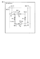
(1) 基本回路
図1は、本開示に係わる不揮発性SRAMセルの基本回路を示している。
第1及び第2のインバーターINV1,INV2は、クロスカップルされる。
(1) Basic circuit
FIG. 1 shows a basic circuit of a nonvolatile SRAM cell according to the present disclosure.
The first and second inverters INV1, INV2 are cross-coupled.
第1のトランジスタ(FET:Field effect transistor)M5は、転送トランジスタであり、そのゲートは、ワード線WLに接続され、そのソースは、第1のビット線BLに接続され、そのドレインは、第2のインバーターINV2の入力端子に接続される。 A first transistor (FET: Field effect transistor) M5 is a transfer transistor, and its gate is connected to the word line WL, its source is connected to the first bit line BL, and its drain is the second transistor. Connected to the input terminal of the inverter INV2.
第2のトランジスタ(FET)M6も、転送トランジスタであり、そのゲートは、ワード線WLに接続され、ソースは、第2のビット線bBLに接続され、ドレインは、第1のインバーターINV1の入力端子に接続される。 The second transistor (FET) M6 is also a transfer transistor, the gate is connected to the word line WL, the source is connected to the second bit line bBL, and the drain is the input terminal of the first inverter INV1. Connected to.
このようなSRAMセルに不揮発にデータを記憶する機能を持たせるために、第1及び第2の可変抵抗素子R1,R2をSRAMセルの要件として追加する。ここで、第1及び第2の可変抵抗素子R1,R2は、セル面積を大きくしないように、以下の接続関係によりSRAMセル内に配置する。 In order to provide such a SRAM cell with a function of storing data in a nonvolatile manner, first and second variable resistance elements R1 and R2 are added as requirements of the SRAM cell. Here, the first and second variable resistance elements R1 and R2 are arranged in the SRAM cell by the following connection relation so as not to increase the cell area.
第1の可変抵抗素子R1の第1の端子(一端)は、第1のトランジスタM5のドレインに接続し、第2の端子(他端)は、第1のインバーターINV1の出力端子に接続する。また、第2の可変抵抗素子R2の第1の端子は、第2のトランジスタM6のドレインに接続し、第2の端子は、第2のインバーターINV2の出力端子に接続する。 The first terminal (one end) of the first variable resistance element R1 is connected to the drain of the first transistor M5, and the second terminal (the other end) is connected to the output terminal of the first inverter INV1. The first terminal of the second variable resistance element R2 is connected to the drain of the second transistor M6, and the second terminal is connected to the output terminal of the second inverter INV2.
このような構成により、セル面積が小さい不揮発性SRAMセルを提供できる。 With such a configuration, a nonvolatile SRAM cell having a small cell area can be provided.
尚、第1及び第2の可変抵抗素子R1,R2は、電流又は電場により抵抗値を変化させることが可能な素子、例えば、スピン注入型MRAM(Spin-injection type magnetic random access memory)に使用される磁気抵抗変化素子、PCRAM(Phase change random access memory)に使用される相変化素子、ReRAM(Resistive random access memory)に使用される抵抗変化素子などである。 The first and second variable resistance elements R1 and R2 are used for elements whose resistance value can be changed by current or electric field, for example, spin injection type MRAM (Spin-injection type magnetic random access memory). Magnetoresistance change elements, phase change elements used for PCRAM (Phase change random access memory), resistance change elements used for ReRAM (Resistive random access memory), and the like.
(2) 基本動作
図1の不揮発性SRAMセルに関しては、リセット/書き込み/読み出しという3つの基本動作モードを有する。また、書き込み/読み出しに関しては、ノーマルモードと不揮発モードとをさらに有する。
(2) Basic operation
The nonvolatile SRAM cell of FIG. 1 has three basic operation modes of reset / write / read. Further, with respect to writing / reading, a normal mode and a nonvolatile mode are further provided.
例えば、図2に示すように、システム(例えば、プロセッサ)1内において、リセット/書き込み/読み出し時における不揮発性SRAMセル2の動作は、制御回路3により制御される。
For example, as shown in FIG. 2, in the system (for example, processor) 1, the operation of the
表1は、リセット/書き込み/読み出し時のワード線WLと第1及び第2のビット線BL,bBLの電位を示している。

A. リセット
リセット動作は、例えば、図3のフローチャートに示すように、データの書き込みの前に行われる。具体的には、データが書き込まれる前に不揮発性SRAMセル内の第1及び第2の可変抵抗素子R1,R2の状態をリセットする(ステップST1)。
A. Reset
The reset operation is performed before data writing, for example, as shown in the flowchart of FIG. Specifically, before the data is written, the states of the first and second variable resistance elements R1 and R2 in the nonvolatile SRAM cell are reset (step ST1).
第1及び第2の可変抵抗素子R1,R2の状態をリセットするとは、第1及び第2の可変抵抗素子R1,R2の抵抗値を同じ(低抵抗値/高抵抗値)にすることを意味する。 Resetting the state of the first and second variable resistance elements R1 and R2 means that the resistance values of the first and second variable resistance elements R1 and R2 are the same (low resistance value / high resistance value). To do.
まず、図2において、不揮発性SRAMセル2を含むシステム1に電源Vddが供給されると、制御回路3が動作状態になる。制御回路3は、第1及び第2のビット線BL,bBLを同一電位に設定し、かつ、第1及び第2のトランジスタM5,M6をオンにすることにより、第1及び第2の可変抵抗素子R1,R2の抵抗値を同一状態にする。
First, in FIG. 2, when the power supply Vdd is supplied to the system 1 including the
A.-1. 第1及び第2の可変抵抗素子R1,R2を同一状態にする場合
例えば、図4に示すように、第1及び第2のビット線BL,bBLを、共に低電位を意味する“L”に設定する。また、ワード線WLを、高電位を意味する“H”に設定して第1及び第2のトランジスタM5,M6をオンにする。
A.-1. When the first and second variable resistance elements R1 and R2 are in the same state
For example, as shown in FIG. 4, both the first and second bit lines BL and bBL are set to “L” which means a low potential. Further, the word line WL is set to “H” which means a high potential, and the first and second transistors M5 and M6 are turned on.
この時、第1の可変抵抗素子R1には、第1のインバーターINV1から第1のビット線BLに向かうリセット電流I1-resetが流れ、第2の可変抵抗素子R2には、第2のインバーターINV2から第2のビット線bBLに向かうリセット電流I2-resetが流れる。 At this time, a reset current I1-reset from the first inverter INV1 toward the first bit line BL flows through the first variable resistance element R1, and the second inverter INV2 flows through the second variable resistance element R2. A reset current I2-reset flows from the first to the second bit line bBL.
その結果、第1及び第2の可変抵抗素子R1,R2の抵抗値は、同一状態(低抵抗状態)になる。 As a result, the resistance values of the first and second variable resistance elements R1 and R2 are in the same state (low resistance state).
B. 書き込み/読み出し
書き込み/読み出し動作は、ノーマルモードと不揮発モードとを備える。
B. Write / Read
The write / read operation includes a normal mode and a nonvolatile mode.
B.-1. ノーマルモード
ノーマルモードは、SRAMセルに揮発的にデータを記憶させるモードである。ノーマルモードでは、書き込み/読み出しは、コンベンショナルなSRAMセルの書き込み/読み出しと同じ動作により行う。
B.-1. Normal mode
The normal mode is a mode in which data is stored volatilely in the SRAM cell. In the normal mode, writing / reading is performed by the same operation as conventional SRAM cell writing / reading.
B.-1.-1. 書き込み
図2において、制御回路3は、書き込みデータDATA,bDATAの値に応じて、第1及び第2のビット線BL,bBLの一方を“H”に設定し、他方を“L”に設定し、ワード線WLを“H”に設定することにより、不揮発性SRAMセル2に揮発データを記憶させる。
B.-1.-1. Writing
In FIG. 2, the
即ち、図5に示すように、第1のビット線BLを第1の電位(“H”/“L”)にし、第1のインバーターINV1の出力端子(ノード)N2を第1の電位にし、第2のビット線bBLを第2の電位(“L”/“H”)にし、第2のインバーターINV2の出力端子(ノード)N4を第2の電位にする。 That is, as shown in FIG. 5, the first bit line BL is set to the first potential (“H” / “L”), the output terminal (node) N2 of the first inverter INV1 is set to the first potential, The second bit line bBL is set to the second potential (“L” / “H”), and the output terminal (node) N4 of the second inverter INV2 is set to the second potential.
例えば、クロスカップルされた2つのインバーターINV1,INV2において、ノードN1,N2が“H”及びノードN3,N4が“L”のとき、書き込みデータDATAとして“1”が記憶され、ノードN1,N2が“L”及びノードN3,N4が“H”のとき、書き込みデータDATAとして“0”が記憶される。 For example, in the two cross-coupled inverters INV1 and INV2, when the nodes N1 and N2 are “H” and the nodes N3 and N4 are “L”, “1” is stored as the write data DATA, and the nodes N1 and N2 are When “L” and nodes N3 and N4 are “H”, “0” is stored as write data DATA.
B.-1.-2. 読み出し
図2において、制御回路3は、ワード線WLを“H”に設定する。この時、SRAMセル2内に記憶されたデータは、読み出しデータDATA,bDATAとして第1及び第2のビット線BL,bBLに出力される。
B.-1.-2. Reading
In FIG. 2, the
B.-2. 不揮発モード
不揮発モードは、SRAMセルのデータを第1及び第2の可変抵抗素子に不揮発に記憶させた後にSRAMセルに対する電源供給を中止し、SRAMセルに対する電源供給を再開した後に、第1及び第2可変抵抗素子に不揮発に記憶されているデータをSRAMセルに呼び戻すモードである。
B.-2. Non-volatile mode
In the non-volatile mode, after the SRAM cell data is stored in the first and second variable resistance elements in a non-volatile manner, the power supply to the SRAM cell is stopped, the power supply to the SRAM cell is resumed, and then the first and second variable In this mode, data stored in the resistance element in a nonvolatile manner is recalled to the SRAM cell.
ここでは、SRAMセルのデータを第1及び第2の可変抵抗素子に不揮発に記憶させる動作を不揮発書き込み(NV-write)動作と称し、第1及び第2可変抵抗素子に不揮発に記憶されているデータをSRAMセルに呼び戻す動作をリコール(recall)動作と称することにする。 Here, the operation of storing the data of the SRAM cell in the first and second variable resistance elements in a nonvolatile manner is referred to as a nonvolatile write (NV-write) operation and is stored in the first and second variable resistance elements in a nonvolatile manner. The operation of recalling data to the SRAM cell will be referred to as a recall operation.
B.-2.-1. 不揮発書き込み(NV-write)
不揮発書き込み動作は、ノーマルモードにおいてSRAMセルに記憶されたデータを保持した状態で実行される。
B.-2.-1. Non-volatile write (NV-write)
The nonvolatile write operation is executed in a state where data stored in the SRAM cell is held in the normal mode.
不揮発書き込み動作は、例えば、以下の二つの場合のいずれかに実行される。 The nonvolatile write operation is executed in one of the following two cases, for example.
第一に、不揮発書き込み動作は、例えば、図6のフローチャートに示すように、システム(例えば、プロセッサ)がスタンバイモードに入るときに行われる。 First, the nonvolatile write operation is performed when a system (for example, a processor) enters a standby mode, for example, as shown in the flowchart of FIG.
具体的には、不揮発性SRAMセルを含むシステムがスタンバイモードになると、第1及び第2の可変抵抗素子R1,R2に対する書き込みを行った後に、不揮発性SRAMセル2への電源供給を中止し、低消費電力化を図る(ステップST1〜ST3)。
Specifically, when the system including the nonvolatile SRAM cell is in the standby mode, after the writing to the first and second variable resistance elements R1 and R2, the power supply to the
第二に、不揮発書き込み動作は、例えば、図7のフローチャートに示すように、ノーマルモードでの書き込みを行った後に行われる。 Second, the nonvolatile write operation is performed after writing in the normal mode, for example, as shown in the flowchart of FIG.
具体的には、不揮発性SRAMセルに対してノーマルモードでの書き込みを行った後に、第1及び第2の可変抵抗素子R1,R2に対する書き込みを行う(ステップST1〜ST2)。その後、図8に示すように、スタンバイモードになると、不揮発性SRAMセル2への電源供給を中止し、低消費電力化を図る(ステップST1〜ST2)。
Specifically, after writing in the normal mode to the nonvolatile SRAM cell, writing to the first and second variable resistance elements R1 and R2 is performed (steps ST1 and ST2). After that, as shown in FIG. 8, when the standby mode is set, the power supply to the
後者の例の場合、スタンバイモードに入った直後に不揮発性書き込みを実行する必要がなくなるため、スタンバイモード時に直ちに不揮発性SRAMセルへの電源供給を遮断し、低消費電力化を図ることができる。 In the case of the latter example, it is not necessary to execute non-volatile writing immediately after entering the standby mode. Therefore, the power supply to the non-volatile SRAM cell can be cut off immediately in the standby mode, thereby reducing power consumption.
また、後者の例では、常に、SRAMセルに不揮発にデータを記憶することになるため、不意な電源遮断に対してもデータを保護することができる。 In the latter example, data is always stored in the SRAM cell in a non-volatile manner, so that data can be protected against unexpected power interruption.
不揮発書き込みでは、まず、図2において、制御回路3は、不揮発性SRAMセル2に揮発データを記憶させた状態で、第1及び第2のビット線BL,bBLを同一電位に設定し、かつ、第1及び第2のトランジスタM5,M6をオンにする。
In nonvolatile writing, first, in FIG. 2, the
この時、第1及び第2の可変抵抗素子R1,R2のうちの1つについては、書き込み電流が流れ(又は電場が印加され)、その抵抗値が変化する。このため、第1及び第2の可変抵抗素子R1,R2の抵抗値が互いに異なり、結果として、不揮発性SRAMセル2に不揮発データが記憶される。
At this time, for one of the first and second variable resistance elements R1 and R2, a write current flows (or an electric field is applied), and the resistance value thereof changes. For this reason, the resistance values of the first and second variable resistance elements R1 and R2 are different from each other, and as a result, nonvolatile data is stored in the
ここで、不揮発書き込みでは、第1及び第2のビット線BL,bBLを共に“H”にする。 Here, in the nonvolatile writing, both the first and second bit lines BL and bBL are set to “H”.
B.-2.-1.-1. 第1及び第2のビット線BL,bBLを“H”にする場合
図4に示すリセット動作により第1及び第2の可変抵抗素子R1,R2が共に低抵抗値にリセットされているときは、この方法により不揮発書き込みを実行する。
B.-2.-1.-1. When the first and second bit lines BL and bBL are set to “H”
When both the first and second variable resistance elements R1 and R2 are reset to low resistance values by the reset operation shown in FIG. 4, nonvolatile writing is executed by this method.
例えば、図9に示すように、ノーマルモード時に不揮発性SRAMセルに“1”が記憶されているとき、ノードN2は、“H”、ノードN4は、“L”である。この状態で、第1及び第2のビット線BL,bBLを、共に“H”に設定し、ワード線WLを“H”に設定して第1及び第2のトランジスタM5,M6をオンにする。 For example, as shown in FIG. 9, when “1” is stored in the nonvolatile SRAM cell in the normal mode, the node N2 is “H” and the node N4 is “L”. In this state, both the first and second bit lines BL and bBL are set to “H”, the word line WL is set to “H”, and the first and second transistors M5 and M6 are turned on. .
この時、第1の可変抵抗素子R1の両端のノードN1,N2は、共に“H”となるため、第1の可変抵抗素子R1には、書き込み電流が流れず(又は電場が印加されず)、第1の可変抵抗素子R1の抵抗値は、変化しない。即ち、第1の可変抵抗素子R1の抵抗値は、第1の抵抗値(低抵抗値)のままである。 At this time, since the nodes N1 and N2 at both ends of the first variable resistance element R1 are both “H”, no write current flows (or no electric field is applied) to the first variable resistance element R1. The resistance value of the first variable resistance element R1 does not change. That is, the resistance value of the first variable resistance element R1 remains the first resistance value (low resistance value).
これに対し、第2の可変抵抗素子R2の一端のノードN3は、“H”となり、他端のノードN4は、“L”となるため、第2の可変抵抗素子R2には、書き込み電流I2-writeが流れ(又は電場が印加され)、第2の可変抵抗素子R2の抵抗値は、変化する。即ち、第2の可変抵抗素子R2の抵抗値は、第1の抵抗値(低抵抗値)から第2の抵抗値(高抵抗値)に変化する。 On the other hand, the node N3 at one end of the second variable resistance element R2 becomes “H” and the node N4 at the other end becomes “L”, and therefore the write current I2 is supplied to the second variable resistance element R2. -write flows (or an electric field is applied), and the resistance value of the second variable resistance element R2 changes. That is, the resistance value of the second variable resistance element R2 changes from the first resistance value (low resistance value) to the second resistance value (high resistance value).
その結果、第2の可変抵抗素子R2の抵抗値が第1の可変抵抗素子R1の抵抗値よりも高い状態になり、不揮発性SRAMセルに“1”が不揮発に記憶される。 As a result, the resistance value of the second variable resistance element R2 becomes higher than the resistance value of the first variable resistance element R1, and “1” is stored in the nonvolatile SRAM cell in a nonvolatile manner.
不揮発書き込みは、ノーマルモード時に不揮発性SRAMセルに保持されているデータに依存して可変抵抗素子への書き込みが行われるため、不揮発書き込みの前にセルのデータをリードして書き戻すといった操作が必要ない。 In nonvolatile writing, writing to the variable resistance element is performed depending on the data held in the nonvolatile SRAM cell in the normal mode. Therefore, it is necessary to read and write back the cell data before nonvolatile writing. Absent.
また、例えば、図10に示すように、ノーマルモード時に不揮発性SRAMセルに“0”が記憶されているとき、ノードN2は、“L”、ノードN4は、“H”である。この状態で、第1及び第2のビット線BL,bBLを、共に“H”に設定し、ワード線WLを“H”に設定して第1及び第2のトランジスタM5,M6をオンにする。 For example, as shown in FIG. 10, when “0” is stored in the nonvolatile SRAM cell in the normal mode, the node N2 is “L” and the node N4 is “H”. In this state, both the first and second bit lines BL and bBL are set to “H”, the word line WL is set to “H”, and the first and second transistors M5 and M6 are turned on. .
この時、第1の可変抵抗素子R1の一端のノードN1は、“H”となり、他端のノードN2は、“L”となるため、第1の可変抵抗素子R1には、書き込み電流I1-writeが流れ(又は電場が印加され)、第1の可変抵抗素子R1の抵抗値は、変化する。即ち、第1の可変抵抗素子R1の抵抗値は、第1の抵抗値(低抵抗値)から第2の抵抗値(高抵抗値)に変化する。 At this time, the node N1 at one end of the first variable resistance element R1 becomes “H” and the node N2 at the other end becomes “L”, so that the write current I1− is applied to the first variable resistance element R1. Write flows (or an electric field is applied), and the resistance value of the first variable resistance element R1 changes. That is, the resistance value of the first variable resistance element R1 changes from the first resistance value (low resistance value) to the second resistance value (high resistance value).
これに対し、第2の可変抵抗素子R2の両端のノードN3,N4は、共に“H”となるため、第2の可変抵抗素子R2には、書き込み電流が流れず(又は電場が印加されず)、第2の可変抵抗素子R2の抵抗値は、変化しない。即ち、第2の可変抵抗素子R2の抵抗値は、第1の抵抗値(低抵抗値)のままである。 On the other hand, since the nodes N3 and N4 at both ends of the second variable resistance element R2 are both “H”, no write current flows (or no electric field is applied to the second variable resistance element R2). ), The resistance value of the second variable resistance element R2 does not change. That is, the resistance value of the second variable resistance element R2 remains the first resistance value (low resistance value).
その結果、第1の可変抵抗素子R1の抵抗値が第2の可変抵抗素子R2の抵抗値よりも高い状態になり、不揮発性SRAMセルに“0”が不揮発に記憶される。 As a result, the resistance value of the first variable resistance element R1 becomes higher than the resistance value of the second variable resistance element R2, and “0” is stored in the nonvolatile SRAM cell in a nonvolatile manner.
B.-2.-2. リコール(Recall)
不揮発性SRAMセルを含むシステムにおいて、スタンバイモードが解除されると、第1及び第2可変抵抗素子に不揮発に記憶されているデータをSRAMセルに呼び戻すリコール動作が実行される。
B.-2.-2. Recall
In a system including a nonvolatile SRAM cell, when the standby mode is canceled, a recall operation for recalling data stored in the first and second variable resistance elements to the SRAM cell is executed.
リコール動作は、ワード線WLを“L”にした状態で、SRAMセル(第1及び第2のインバーターINV1,INV2)に電源Vddを供給することにより自動的に行われる。 The recall operation is automatically performed by supplying power Vdd to the SRAM cells (first and second inverters INV1 and INV2) with the word line WL set to “L”.
B.-2.-2.-1. R1<R2の場合
不揮発書き込みにより、第1の可変抵抗素子R1が低抵抗値、第2の可変抵抗素子R2が高抵抗値の状態になっている場合を説明する。この状態は、不揮発性SRAMセルに“1”が不揮発に記憶されている状態である。
B.-2.-2.-1. When R1 <R2
A case where the first variable resistance element R1 is in a low resistance value and the second variable resistance element R2 is in a high resistance value due to nonvolatile writing will be described. This state is a state in which “1” is stored in the nonvolatile SRAM cell in a nonvolatile manner.
この場合、図11に示すように、インバーターINV1,INV2に電源Vddが供給されると、まず、インバーターINV1,INV2にリーク電流が流れ、インバーターINV1,INV2の出力端子(ノード)N2,N4の電位が上昇する。 In this case, as shown in FIG. 11, when the power supply Vdd is supplied to the inverters INV1 and INV2, first, a leakage current flows through the inverters INV1 and INV2, and the potentials of the output terminals (nodes) N2 and N4 of the inverters INV1 and INV2 Rises.
この後、ノードN1,N3の電位が上昇する。 Thereafter, the potentials of nodes N1 and N3 rise.
この時、第2の可変抵抗素子R2の抵抗値は、第1の可変抵抗素子R1の抵抗値よりも高いため、ノードN4の電位がノードN3に伝わる速度は、ノードN2の電位がノードN1に伝わる速度よりも遅い。 At this time, since the resistance value of the second variable resistance element R2 is higher than the resistance value of the first variable resistance element R1, the speed at which the potential of the node N4 is transmitted to the node N3 is the same as the potential of the node N2 to the node N1. Slower than transmission speed.
このため、インバーターINV2の入力端子(ノード)N1は、インバーターINV1の入力端子(ノード)N3よりも先に“H”になる。 For this reason, the input terminal (node) N1 of the inverter INV2 becomes “H” before the input terminal (node) N3 of the inverter INV1.
従って、ノードN1,N2が“H”になり、ノードN3,N4が“L”になり、不揮発性SRAMセルにデータ“1”が正確に呼び戻される。 Therefore, the nodes N1 and N2 become “H”, the nodes N3 and N4 become “L”, and the data “1” is accurately recalled to the nonvolatile SRAM cell.
B.-2.-2.-2. R1>R2の場合
不揮発書き込みにより、第1の可変抵抗素子R1が高抵抗値、第2の可変抵抗素子R2が低抵抗値の状態になっている場合を説明する。この状態は、不揮発性SRAMセルに“0”が不揮発に記憶されている状態である。
B.-2.-2.-2. When R1> R2
A case where the first variable resistance element R1 is in a high resistance value and the second variable resistance element R2 is in a low resistance value due to nonvolatile writing will be described. This state is a state in which “0” is stored in the nonvolatile SRAM cell in a nonvolatile manner.
この場合、図12に示すように、インバーターINV1,INV2に電源Vddが供給されると、まず、インバーターINV1,INV2にリーク電流が流れ、インバーターINV1,INV2の出力端子(ノード)N2,N4の電位が上昇する。 In this case, as shown in FIG. 12, when the power supply Vdd is supplied to the inverters INV1 and INV2, first, a leakage current flows through the inverters INV1 and INV2, and the potentials of the output terminals (nodes) N2 and N4 of the inverters INV1 and INV2 Rises.
この後、ノードN1,N3の電位が上昇する。 Thereafter, the potentials of nodes N1 and N3 rise.
この時、第1の可変抵抗素子R1の抵抗値は、第2の可変抵抗素子R2の抵抗値よりも高いため、ノードN2の電位がノードN1に伝わる速度は、ノードN4の電位がノードN3に伝わる速度よりも遅い。 At this time, since the resistance value of the first variable resistance element R1 is higher than the resistance value of the second variable resistance element R2, the speed at which the potential of the node N2 is transmitted to the node N1 is the same as that of the node N4. Slower than transmission speed.
このため、インバーターINV1の入力端子(ノード)N3は、インバーターINV2の入力端子(ノード)N1よりも先に“H”になる。 Therefore, the input terminal (node) N3 of the inverter INV1 becomes “H” before the input terminal (node) N1 of the inverter INV2.
従って、ノードN1,N2が“L”になり、ノードN3,N4が“H”になり、不揮発性SRAMセルにデータ“0”が正確に呼び戻される。 Accordingly, the nodes N1 and N2 become “L”, the nodes N3 and N4 become “H”, and the data “0” is accurately recalled to the nonvolatile SRAM cell.
(3) まとめ
以上、本開示によれば、セル面積が小さい、即ち、揮発性SRAMセルと同じトランジスタ数の基本回路と、スタンバイモード時における低消費電力化を実現するための基本動作とを備える不揮発性SRAMセルを実現できる。
(3) Summary
As described above, according to the present disclosure, a nonvolatile SRAM cell having a small cell area, that is, a basic circuit having the same number of transistors as that of a volatile SRAM cell and a basic operation for realizing low power consumption in the standby mode. Can be realized.
2. 実施例
(1) 第1の実施例
図13は、第1の実施例を示している。
2. Example
(1) First embodiment
FIG. 13 shows a first embodiment.
不揮発性SRAMセルは、第1及び第2のインバーターINV1,INV2と、ゲートにワード線WLが接続され、ソースに第1のビット線BLが接続され、ドレインに第2のインバーターINV2の入力端子が接続される第1のトランジスタM5と、ゲートにワード線WLが接続され、ソースに第2のビット線BLBが接続され、ドレインに第1のインバーターINV1の入力端子が接続される第2のトランジスタM6とを備える。 The nonvolatile SRAM cell has first and second inverters INV1 and INV2, a gate connected to the word line WL, a source connected to the first bit line BL, and a drain connected to the input terminal of the second inverter INV2. The first transistor M5 to be connected, the second transistor M6 having the gate connected to the word line WL, the source connected to the second bit line BLB, and the drain connected to the input terminal of the first inverter INV1. With.
さらに、不揮発性SRAMセルは、第1の端子に第1のトランジスタM5のドレインが接続され、第2の端子に第1のインバーターINV1の出力端子が接続される第1の磁気抵抗効果素子MTJ1と、第1の端子に第2のトランジスタM6のドレインが接続され、第2の端子に第2のインバーターINV2の出力端子が接続される第2の磁気抵抗効果素子MTJ2とを備える。 Further, the nonvolatile SRAM cell includes a first magnetoresistive element MTJ1 having a first terminal connected to the drain of the first transistor M5 and a second terminal connected to the output terminal of the first inverter INV1. , And a second magnetoresistive element MTJ2 having the first terminal connected to the drain of the second transistor M6 and the second terminal connected to the output terminal of the second inverter INV2.
第1のインバーターINV1は、2つの電源端子Vdd,Vssの間に直列接続されるPチャネルMOSFET M1及びNチャネルMOSFET M2から構成される。また、第2のインバーターINV2は、2つの電源端子Vdd,Vssの間に直列接続されるPチャネルMOSFET M3及びNチャネルMOSFET M4から構成される。 The first inverter INV1 includes a P-channel MOSFET M1 and an N-channel MOSFET M2 connected in series between the two power supply terminals Vdd and Vss. The second inverter INV2 includes a P-channel MOSFET M3 and an N-channel MOSFET M4 connected in series between the two power supply terminals Vdd and Vss.
第1及び第2の磁気抵抗効果素子MTJ1,MTJ2の各々は、磁化固着層(Magnetic pinned layer)11、磁化自由層(Magnetic free layer)12及びそれらの間のトンネル絶縁層(Tunnel insulating layer)13を備えるスピン注入方式の磁気抵抗変化素子である。
Each of the first and second magnetoresistance effect elements MTJ1 and MTJ2 includes a magnetic pinned
第1の磁気抵抗効果素子MTJ1の磁化固着層11は、第1のインバーターINV1の出力端子に接続され、第1の磁気抵抗効果素子MTJ1の磁化自由層12は、第1のトランジスタM5のドレインに接続される。
The magnetization pinned
第2の磁気抵抗効果素子MTJ2の磁化固着層11は、第2のインバーターINV2の出力端子に接続され、第2の磁気抵抗効果素子MTJ2の磁化自由層12は、第2のトランジスタM6のドレインに接続される。
The magnetization pinned
第1及び第2の磁気抵抗効果素子MTJ1,MTJ2は、それぞれ、磁化固着層11から磁化自由層12に書き込み電流を流すと、高抵抗値から低抵抗値に変化し、磁化自由層12から磁化固着層11に書き込み電流を流すと、低抵抗値から高抵抗値に変化するものとする。
Each of the first and second magnetoresistance effect elements MTJ1 and MTJ2 changes from a high resistance value to a low resistance value when a write current is passed from the magnetization fixed
この構成において、ワード線WL、第1及び第2のビット線BL,bBLの電位を制御して、リセット/書き込み/読み出しを実行する。 In this configuration, reset / write / read is executed by controlling the potential of the word line WL and the first and second bit lines BL, bBL.
図14は、図13の不揮発性SRAMセルの動作の第1例を示している。 FIG. 14 shows a first example of the operation of the nonvolatile SRAM cell of FIG.
リセット動作では、ワード線WLを“H”にし、第1及び第2のビット線BL,bBLを“L”にする。この時、第1及び第2の磁気抵抗効果素子MTJ1,MTJ2では、共に、磁化固着層11から磁化自由層12に向かって書き込み電流が流れるため、第1及び第2の磁気抵抗効果素子MTJ1,MTJ2は、共に、低抵抗値になる。リセット電流が磁気抵抗効果素子MTJ1,MTJ2の書き込み電流に対して不足する場合は、図14に示すように、電源Vddは、通常の電源電位Vddよりも高い電位にすることで対処できる。
In the reset operation, the word line WL is set to “H”, and the first and second bit lines BL and bBL are set to “L”. At this time, in both the first and second magnetoresistive effect elements MTJ1 and MTJ2, a write current flows from the magnetization fixed
ノーマルモードでの書き込み/読み出しは、揮発性SRAMセルと同様に行う。 Writing / reading in the normal mode is performed in the same manner as the volatile SRAM cell.
書き込みでは、例えば、ワード線WLを“H”にし、第1のビット線BLを“H”にし、第2のビット線bBLを“L”にし、不揮発性SRAMセルに“1”(ノードN1,N2=“H”、ノードN3,N4=“L”)を記憶させる。 In writing, for example, the word line WL is set to “H”, the first bit line BL is set to “H”, the second bit line bBL is set to “L”, and “1” (nodes N1, N1) is input to the nonvolatile SRAM cell. N2 = "H", nodes N3, N4 = "L") are stored.
また、読み出しでは、予め、第1及び第2のビット線BL,bBLをプリチャージしておき、その後、ワード線を“H”にし、第1及び第2のビット線BL,bBLに電位差を生じさせる。この電位差をセンスアンプによりセンスすることによりSRAMセルのデータを読み出すことができる。 In reading, the first and second bit lines BL and bBL are precharged in advance, and then the word line is set to “H” to generate a potential difference between the first and second bit lines BL and bBL. Let The SRAM cell data can be read by sensing this potential difference with a sense amplifier.
尚、書き込み/読み出し時において、第1及び第2の磁気抵抗効果素子MTJ1,MTJ2には電流が流れる。 In writing / reading, a current flows through the first and second magnetoresistive elements MTJ1, MTJ2.
しかし、書き込み時に第1及び第2の磁気抵抗効果素子MTJ1,MTJ2に電流が流れる時間は、0.1 psec程度である。 However, the time during which a current flows through the first and second magnetoresistive elements MTJ1 and MTJ2 during writing is about 0.1 psec.
また、読み出し時に第1及び第2の磁気抵抗効果素子MTJ1,MTJ2に電流が流れる時間は、トランジスタの世代と、低抵抗状態にリセットされている磁気抵抗効果素子の抵抗値と、センスアンプまでのBL,bBLの配線抵抗値、配線容量値などに依存する。例えば、65nm世代において、低抵抗状態にリセットされている磁気抵抗効果素子の抵抗値を、4kΩ、センスアンプまでのビット線対BL,bBLの配線抵抗値、配線容量値を、それぞれ約200Ω、約14fFとすると、50uA以上の電流が流れる時間は、約1.5nsec程度である。 In addition, the time during which current flows through the first and second magnetoresistive elements MTJ1 and MTJ2 at the time of reading is the generation of the transistor, the resistance value of the magnetoresistive element reset to the low resistance state, and the sense amplifier It depends on the wiring resistance values and wiring capacitance values of BL and bBL. For example, in the 65 nm generation, the resistance value of the magnetoresistive effect element reset to the low resistance state is 4 kΩ, and the wiring resistance value and wiring capacitance value of the bit line pair BL, bBL up to the sense amplifier are about 200Ω, about Assuming 14 fF, the time during which a current of 50 uA or more flows is about 1.5 nsec.
このため、ノーマルモードでの書き込み/読み出し時に、第1及び第2の磁気抵抗効果素子MTJ1,MTJ2に対する書き込みが行われることはない。また、書き込みが行われることが予測される場合は、上記の配線条件などを変えることにより回避できる。さらに、読み出し時に第1及び第2の磁気抵抗効果素子MTJ1,MTJ2に電流が流れる方向は、不揮発書き込みの時の書き込み電流が流れる条件と同じであるため、書き込みが行われても問題は無い。 For this reason, at the time of writing / reading in the normal mode, writing to the first and second magnetoresistive elements MTJ1, MTJ2 is not performed. In addition, when it is predicted that writing will be performed, it can be avoided by changing the above wiring conditions. Furthermore, since the direction in which the current flows in the first and second magnetoresistive elements MTJ1 and MTJ2 during reading is the same as the condition in which the write current flows during nonvolatile writing, there is no problem even if writing is performed.
システムがスタンバイモードとなると、不揮発性SRAMセルへの電源供給を遮断する前に、不揮発書き込みを実行する。 When the system enters the standby mode, nonvolatile writing is executed before the power supply to the nonvolatile SRAM cell is cut off.
不揮発書き込みでは、例えば、ワード線WLを“H”にし、第1及び第2のビット線BL,bBLを“H”にし、第1及び第2の磁気抵抗効果素子MTJ1,MTJ2に対する書き込みを実行する。 In nonvolatile writing, for example, the word line WL is set to “H”, the first and second bit lines BL and bBL are set to “H”, and writing to the first and second magnetoresistive elements MTJ1 and MTJ2 is executed. .
本例では、ノーマルモードの書き込みにおいて不揮発性SRAMセルが“1”を記憶するため、不揮発書き込みでは、第1の磁気抵抗効果素子MTJ1を低抵抗値とし、第2の磁気抵抗効果素子MTJ2を高抵抗値とする。 In this example, since the nonvolatile SRAM cell stores “1” in the normal mode writing, the first magnetoresistive element MTJ1 is set to a low resistance value and the second magnetoresistive element MTJ2 is set to a high value in the nonvolatile writing. Resistance value.
具体的には、不揮発性SRAMセルが“1”を記憶しているとき、ノードN1,N2が“H”、ノードN3,N4が“L”である。このため、第1及び第2のビット線BL,bBLを“H”にすると、第2の磁気抵抗効果素子MTJ2のみに、磁化自由層12から磁化固着層11に向かう書き込み電流が流れる。書き込み電流が磁気抵抗効果素子MTJ2の書き込み電流に対して不足する場合は、図14に示すように、ワード線WLの電位は、通常の電源電位Vddよりも高い電位にすることで対処できる。
Specifically, when the nonvolatile SRAM cell stores “1”, the nodes N1 and N2 are “H” and the nodes N3 and N4 are “L”. Therefore, when the first and second bit lines BL and bBL are set to “H”, a write current from the magnetization
従って、第1の磁気抵抗効果素子MTJ1は、低抵抗値のままとなり、第2の磁気抵抗効果素子MTJ2は、低抵抗値から高抵抗値に変化する。 Accordingly, the first magnetoresistance effect element MTJ1 remains at a low resistance value, and the second magnetoresistance effect element MTJ2 changes from a low resistance value to a high resistance value.
不揮発書き込みが終了すると、不揮発性SRAMセルへの電源供給が遮断される。 When nonvolatile writing is completed, power supply to the nonvolatile SRAM cell is interrupted.
スタンバイモードが終了し、不揮発性SRAMセルへの電源供給が再開されると、リコールが実行される。 When the standby mode ends and the power supply to the nonvolatile SRAM cell is resumed, the recall is executed.
不揮発性SRAMセルへの電源供給により、インバーターINV1,INV2に電源Vddが印加されると、まず、インバーターINV1,INV2にリーク電流が流れ、インバーターINV1,INV2の出力端子(ノード)N2,N4の電位が上昇する。 When the power supply Vdd is applied to the inverters INV1 and INV2 by supplying power to the nonvolatile SRAM cell, first, a leakage current flows through the inverters INV1 and INV2, and the potentials of the output terminals (nodes) N2 and N4 of the inverters INV1 and INV2 Rises.
この後、ノードN1,N3の電位が上昇する。 Thereafter, the potentials of nodes N1 and N3 rise.
この時、第2の磁気抵抗効果素子MTJ2の抵抗値は、第1の磁気抵抗効果素子MTJ1の抵抗値よりも高いため、ノードN4の電位がノードN3に伝わる速度は、ノードN2の電位がノードN1に伝わる速度よりも遅い。 At this time, since the resistance value of the second magnetoresistive element MTJ2 is higher than the resistance value of the first magnetoresistive element MTJ1, the speed at which the potential of the node N4 is transmitted to the node N3 is Slower than the speed transmitted to N1.
このため、インバーターINV2の入力端子(ノード)N1は、インバーターINV1の入力端子(ノード)N3よりも先に“H”になる。 For this reason, the input terminal (node) N1 of the inverter INV2 becomes “H” before the input terminal (node) N3 of the inverter INV1.
従って、ノードN1,N2が“H”になり、ノードN3,N4が“L”になり、不揮発性SRAMセルに“1”が呼び戻される。 Therefore, the nodes N1 and N2 become “H”, the nodes N3 and N4 become “L”, and “1” is recalled to the nonvolatile SRAM cell.
ところで、先端プロセスを用いたLSIでは、トランジスタの閾値ばらつきが大きくなることが問題となっている。トランジスタの閾値ばらつきが大きいと、誤データをリコールしてしまう場合がある。これを防止するために、図15に示す方法を採用してもよい。 By the way, in the LSI using the advanced process, there is a problem that the threshold variation of the transistor becomes large. If the threshold variation of transistors is large, erroneous data may be recalled. In order to prevent this, the method shown in FIG. 15 may be adopted.
この方法の特徴は、第1及び第2のビット線BL,bBLを“L”に維持した状態で、ワード線WLを“L”→“H”→“L”に変化させる点にある。 This method is characterized in that the word line WL is changed from “L” → “H” → “L” in a state where the first and second bit lines BL and bBL are maintained at “L”.
ワード線WLが“L”、第1及び第2のビット線BL,bBLが“L”の状態で、SRAMセルに電源が供給されると、トランジスタの閾値ばらつきに依存したデータがリコールされる。この後、ワード線WLを“L”→“H”→“L”と変化させると、低抵抗値を有する磁気抵抗効果素子の両端の電位が、高抵抗値を有する磁気抵抗効果素子の両端の電位よりも高くなり、正確にリコールが実行される。 When power is supplied to the SRAM cell in a state where the word line WL is “L” and the first and second bit lines BL and bBL are “L”, data depending on the threshold variation of the transistors is recalled. Thereafter, when the word line WL is changed from “L” → “H” → “L”, the potentials at both ends of the magnetoresistive effect element having a low resistance value are changed between the both ends of the magnetoresistive effect element having a high resistance value. It becomes higher than the electric potential, and the recall is executed accurately.
(2) 第2の実施例
図17は、第2の実施例を示している。
(2) Second embodiment
FIG. 17 shows a second embodiment.
第2の実施例が第1の実施例と異なる点は、第1及び第2の磁気抵抗効果素子MTJ1,MTJ2の磁化固着層/磁化自由層の位置が逆になっていることにある。 The second embodiment is different from the first embodiment in that the positions of the magnetization fixed layer / magnetization free layer of the first and second magnetoresistance effect elements MTJ1 and MTJ2 are reversed.
不揮発性SRAMセルは、第1及び第2のインバーターINV1,INV2と、ゲートにワード線WLが接続され、ソースに第1のビット線BLが接続され、ドレインに第2のインバーターINV2の入力端子が接続される第1のトランジスタM5と、ゲートにワード線WLが接続され、ソースに第2のビット線BLBが接続され、ドレインに第1のインバーターINV1の入力端子が接続される第2のトランジスタM6とを備える。 The nonvolatile SRAM cell has first and second inverters INV1 and INV2, a gate connected to the word line WL, a source connected to the first bit line BL, and a drain connected to the input terminal of the second inverter INV2. The first transistor M5 to be connected, the second transistor M6 having the gate connected to the word line WL, the source connected to the second bit line BLB, and the drain connected to the input terminal of the first inverter INV1. With.
さらに、不揮発性SRAMセルは、第1の端子に第1のトランジスタM5のドレインが接続され、第2の端子に第1のインバーターINV1の出力端子が接続される第1の磁気抵抗効果素子MTJ1と、第1の端子に第2のトランジスタM6のドレインが接続され、第2の端子に第2のインバーターINV2の出力端子が接続される第2の磁気抵抗効果素子MTJ2とを備える。 Further, the nonvolatile SRAM cell includes a first magnetoresistive element MTJ1 having a first terminal connected to the drain of the first transistor M5 and a second terminal connected to the output terminal of the first inverter INV1. , And a second magnetoresistive element MTJ2 having the first terminal connected to the drain of the second transistor M6 and the second terminal connected to the output terminal of the second inverter INV2.
第1のインバーターINV1は、2つの電源端子Vdd,Vssの間に直列接続されるPチャネルMOSFET M1及びNチャネルMOSFET M2から構成される。また、第2のインバーターINV2は、2つの電源端子Vdd,Vssの間に直列接続されるPチャネルMOSFET M3及びNチャネルMOSFET M4から構成される。 The first inverter INV1 includes a P-channel MOSFET M1 and an N-channel MOSFET M2 connected in series between the two power supply terminals Vdd and Vss. The second inverter INV2 includes a P-channel MOSFET M3 and an N-channel MOSFET M4 connected in series between the two power supply terminals Vdd and Vss.
第1及び第2の磁気抵抗効果素子MTJ1,MTJ2の各々は、磁化固着層11、磁化自由層12及びそれらの間のトンネル絶縁層13を備えるスピン注入方式の磁気抵抗変化素子である。
Each of the first and second magnetoresistive effect elements MTJ1 and MTJ2 is a spin-injection magnetoresistive change element including a fixed
第1の磁気抵抗効果素子MTJ1の磁化固着層11は、第1のトランジスタM5のドレインに接続され、第1の磁気抵抗効果素子MTJ1の磁化自由層12は、第1のインバーターINV1の出力端子に接続される。
The magnetization pinned
第2の磁気抵抗効果素子MTJ2の磁化固着層11は、第2のトランジスタM6のドレインに接続され、第2の磁気抵抗効果素子MTJ2の磁化自由層12は、第2のインバーターINV2の出力端子に接続される。
The pinned
第1及び第2の磁気抵抗効果素子MTJ1,MTJ2は、それぞれ、磁化固着層11から磁化自由層12に書き込み電流を流すと、高抵抗値から低抵抗値に変化し、磁化自由層12から磁化固着層11に書き込み電流を流すと、低抵抗値から高抵抗値に変化するものとする。
Each of the first and second magnetoresistance effect elements MTJ1 and MTJ2 changes from a high resistance value to a low resistance value when a write current is passed from the magnetization fixed
この構成において、ワード線WL、第1及び第2のビット線BL,bBLの電位を制御して、リセット/書き込み/読み出しを実行する。 In this configuration, reset / write / read is executed by controlling the potential of the word line WL and the first and second bit lines BL, bBL.
書き込み/読み出しは、第1の実施例(図14〜図15)と同様に行うことができるので、ここでは、その詳細な説明を省略する。 Since writing / reading can be performed in the same manner as in the first embodiment (FIGS. 14 to 15), detailed description thereof is omitted here.
図16は、図17の不揮発性SRAMセルの動作を示している。
第2の実施例の特徴は、ノーマルモードでの書き込みを行った後に、不揮発モードでの書き込み(不揮発書き込み)を続けて行うことにある。本実施例では、リセット後の状態より不揮発書き込みを行った後の状態の方がStatic Noise Margin(SNM)が大きく、安定であるため、ノーマルモードでの書き込みを行った後に、不揮発書き込みを続けて行うことが望ましい。しかし、続けて行うことでシステムのパフォーマンスが落ちるなど問題がある場合は、他からのアクセスの無い空いた時間に不揮発書き込みを行っても良い。
FIG. 16 shows the operation of the nonvolatile SRAM cell of FIG.
The feature of the second embodiment is that writing in the non-volatile mode (non-volatile writing) is continuously performed after writing in the normal mode. In this embodiment, since the state after the nonvolatile writing is larger than the state after the reset and the static noise margin (SNM) is larger and stable, the nonvolatile writing is continued after the writing in the normal mode. It is desirable to do. However, if there is a problem such as a decrease in system performance due to continuous execution, non-volatile writing may be performed at a free time when there is no other access.
この場合、スタンバイモードに入ってから不揮発性書き込みを実行する必要がなくなるため、スタンバイモード時に直ちに不揮発性SRAMセルへの電源供給を遮断し、低消費電力化を図ることができる。 In this case, since it is not necessary to execute nonvolatile writing after entering the standby mode, power supply to the nonvolatile SRAM cell can be cut off immediately in the standby mode, thereby reducing power consumption.
また、第2の実施例では、常に、SRAMセルに不揮発にデータを記憶することになるため、不意な電源遮断に対してもデータを保護することができる。 In the second embodiment, since data is always stored in the SRAM cell in a nonvolatile manner, the data can be protected against unexpected power interruption.
リセット動作では、ワード線WLを“H”にし、第1及び第2のビット線BL,bBLを“L”にする。この時、第1及び第2の磁気抵抗効果素子MTJ1,MTJ2では、共に、磁化自由層12から磁化固着層11に向かって書き込み電流が流れるため、第1及び第2の磁気抵抗効果素子MTJ1,MTJ2は、共に、高抵抗値になる。リセット電流が磁気抵抗効果素子MTJ1,MTJ2の書き込み電流に対して不足する場合は、図14に示すように、電源Vddは、通常の電源電位Vddよりも高い電位にすることで対処できる。
In the reset operation, the word line WL is set to “H”, and the first and second bit lines BL and bBL are set to “L”. At this time, in both the first and second magnetoresistance effect elements MTJ1 and MTJ2, a write current flows from the magnetization
尚、書き込み/読み出しは、第1の実施例(図14)のそれと同じであるため、ここではその説明の詳細を省略する。 Since writing / reading is the same as that in the first embodiment (FIG. 14), the details of the description are omitted here.
不揮発書き込みでは、例えば、ワード線WLを“H”にし、第1及び第2のビット線BL,bBLを“H”にし、第1及び第2の磁気抵抗効果素子MTJ1,MTJ2に対する書き込みを実行する。 In nonvolatile writing, for example, the word line WL is set to “H”, the first and second bit lines BL and bBL are set to “H”, and writing to the first and second magnetoresistive elements MTJ1 and MTJ2 is executed. .
本例では、ノーマルモードの書き込みにおいて不揮発性SRAMセルが“1”を記憶するため、不揮発書き込みでは、第1の磁気抵抗効果素子MTJ1を高抵抗値とし、第2の磁気抵抗効果素子MTJ2を低抵抗値とする。 In this example, since the nonvolatile SRAM cell stores “1” in the normal mode writing, the first magnetoresistive element MTJ1 is set to a high resistance value and the second magnetoresistive element MTJ2 is set to a low value in the nonvolatile writing. Resistance value.
具体的には、不揮発性SRAMセルが“1”を記憶しているとき、ノードN1,N2が“H”、ノードN3,N4が“L”である。このため、第1及び第2のビット線BL,bBLを“H”にすると、第2の磁気抵抗効果素子MTJ2のみに、磁化固着層11から磁化自由層12に向かう書き込み電流が流れる。書き込み電流が磁気抵抗効果素子MTJ2の書き込み電流に対して不足する場合は、図17に示すように、ワード線WLの電位は、通常の電源電位Vddよりも高い電位にすることで対処できる。
Specifically, when the nonvolatile SRAM cell stores “1”, the nodes N1 and N2 are “H” and the nodes N3 and N4 are “L”. For this reason, when the first and second bit lines BL and bBL are set to “H”, a write current from the magnetization fixed
従って、第1の磁気抵抗効果素子MTJ1は、高抵抗値のままとなり、第2の磁気抵抗効果素子MTJ2は、高抵抗値から低抵抗値に変化する。 Therefore, the first magnetoresistance effect element MTJ1 remains at a high resistance value, and the second magnetoresistance effect element MTJ2 changes from a high resistance value to a low resistance value.
リコールについては、電源Vddを2段階で上昇させる方法を採用する。 For the recall, a method of raising the power supply Vdd in two stages is adopted.
例えば、まず、ワード線WLを“L”にし、第1及び第2のビット線BL,bBLを“L”にした状態で、電源Vddを第1のレベル(V-recall)まで上昇させ、トランジスタの閾値ばらつきに依存したデータをリコールする。第1のレベルは、(電源VddのHレベル)−(NチャネルMOSFETの閾値電圧Vthn)より小さい値とする。 For example, first, with the word line WL set to “L” and the first and second bit lines BL and bBL set to “L”, the power supply Vdd is raised to the first level (V-recall), and the transistor Recall data that depends on threshold variation. The first level is a value smaller than (H level of power supply Vdd) − (threshold voltage Vthn of N-channel MOSFET).
この後、第1及び第2のビット線BL,bBLを“H”にする。続けて、ワード線WLを“L”→“H”→“L”と変化させると、低抵抗値を有する磁気抵抗効果素子の両端の電位が、高抵抗値を有する磁気抵抗効果素子の両端の電位よりも低く、電源Vddを第2のレベル(“H”)にすると、高抵抗値を有する磁気抵抗効果素子の両端の電位が“H”、低抵抗値を有する磁気抵抗効果素子の両端の電位が“L”に確定し、正確にリコールが実行される。 Thereafter, the first and second bit lines BL and bBL are set to “H”. Subsequently, when the word line WL is changed from “L” → “H” → “L”, the potentials at both ends of the magnetoresistive effect element having a low resistance value are changed between the both ends of the magnetoresistive effect element having a high resistance value. When the power supply Vdd is lower than the potential and the power supply Vdd is set to the second level (“H”), the potentials at both ends of the magnetoresistive effect element having a high resistance value are “H”, The potential is fixed at “L” and the recall is executed accurately.
上述の方法は、不揮発性SRAMセルを複数のワード線からなるマトリックス状に配置し、電源Vddを共通に制御する場合に適している。例えば、ワード線WL1からワード線WL10まであるマトリックスの場合、電源Vddを第1のレベルまで上げた後、“L”→“H”→“L”の変化をワード線WL1からワード線WL10まで順に行う。その後、電源Vddを第2のレベル(“H”)にし、ワード線WL1からワード線WL10につながる全ての不揮発性SRAMセルのリコールを終了する。 The above-described method is suitable for the case where nonvolatile SRAM cells are arranged in a matrix made up of a plurality of word lines and the power supply Vdd is controlled in common. For example, in the case of a matrix having the word line WL1 to the word line WL10, after the power supply Vdd is raised to the first level, the change of “L” → “H” → “L” is sequentially performed from the word line WL1 to the word line WL10. Do. Thereafter, the power supply Vdd is set to the second level (“H”), and the recall of all nonvolatile SRAM cells connected from the word line WL1 to the word line WL10 is completed.
不揮発性SRAMセルを上述のようなマトリックス状に配置しない、または、電源Vddを共通に制御しない場合は、必ずしも2段階で上昇させる必要は無い。 When the non-volatile SRAM cells are not arranged in a matrix as described above, or when the power supply Vdd is not controlled in common, it is not always necessary to raise in two steps.
具体的には、まず第1及び第2のビット線BL,bBLを“L”にした状態で、ワード線WLを“L”→“H”と変化させる。その後、電源Vddを“H”まで上昇させると、高抵抗値を有する磁気抵抗効果素子の両端の電位が“H”、低抵抗値を有する磁気抵抗効果素子の両端の電位が“L”に確定する。データの確定が確実になった時点でワード線WLを“H”→“L”とし、ワード線WLにつながる全ての不揮発性SRAMセルのリコールを終了する。 Specifically, first, the word line WL is changed from “L” to “H” in a state where the first and second bit lines BL and bBL are set to “L”. Thereafter, when the power supply Vdd is raised to “H”, the potentials at both ends of the magnetoresistive effect element having a high resistance value are determined to be “H” and the potentials at both ends of the magnetoresistive effect element having a low resistance value are determined to be “L”. To do. When the data is confirmed, the word line WL is changed from “H” to “L”, and the recall of all nonvolatile SRAM cells connected to the word line WL is completed.
(3) 第3の実施例
図18は、第3の実施例を示している。
(3) Third embodiment
FIG. 18 shows a third embodiment.
第3の実施例の特徴は、第1及び第2のビット線BL,bBLの電位を等しくするイコライザを有する点にある。不揮発書き込みでは、第1及び第2のビット線BL,bBLの電位を等しくすることが前提となるため、このイコライザは、不揮発書き込みを正確に行うに当たって非常に有効である。 The feature of the third embodiment is that it has an equalizer for equalizing the potentials of the first and second bit lines BL and bBL. In nonvolatile writing, since it is premised on that the potentials of the first and second bit lines BL and bBL are equal, this equalizer is very effective in accurately performing nonvolatile writing.
このイコライザは、コンベンショナルなSRAMに備えられているイコライザをそのまま利用してもよい。 As this equalizer, an equalizer provided in a conventional SRAM may be used as it is.
不揮発性SRAMセルは、第1及び第2のインバーターINV1,INV2と、ゲートにワード線WLが接続され、ソースに第1のビット線BLが接続され、ドレインに第2のインバーターINV2の入力端子が接続される第1のトランジスタM5と、ゲートにワード線WLが接続され、ソースに第2のビット線BLBが接続され、ドレインに第1のインバーターINV1の入力端子が接続される第2のトランジスタM6とを備える。 The nonvolatile SRAM cell has first and second inverters INV1 and INV2, a gate connected to the word line WL, a source connected to the first bit line BL, and a drain connected to the input terminal of the second inverter INV2. The first transistor M5 to be connected, the second transistor M6 having the gate connected to the word line WL, the source connected to the second bit line BLB, and the drain connected to the input terminal of the first inverter INV1. With.
また、不揮発性SRAMセルは、第1の端子に第1のトランジスタM5のドレインが接続され、第2の端子に第1のインバーターINV1の出力端子が接続される第1の可変抵抗素子R1と、第1の端子に第2のトランジスタM6のドレインが接続され、第2の端子に第2のインバーターINV2の出力端子が接続される第2の可変抵抗素子R2とを備える。 The nonvolatile SRAM cell includes a first variable resistance element R1 having a first terminal connected to the drain of the first transistor M5 and a second terminal connected to the output terminal of the first inverter INV1. A second variable resistance element R2 having a first terminal connected to a drain of the second transistor M6 and a second terminal connected to an output terminal of the second inverter INV2.
さらに、不揮発性SRAMセルは、ソース/ドレインに第1及び第2のビット線BL,bBLが接続され、ゲートに制御信号NVWEQが入力される第3のトランジスタ(FET)M7を備える。制御信号NVWEQは、例えば、不揮発書き込み時に“H”となり、第1及び第2のビット線BL,bBLの電位を等しくする。 Further, the nonvolatile SRAM cell includes a third transistor (FET) M7 having first and second bit lines BL and bBL connected to the source / drain and a control signal NVWEQ input to the gate. For example, the control signal NVWEQ becomes “H” during nonvolatile writing, and the potentials of the first and second bit lines BL and bBL are made equal.
第1のインバーターINV1は、2つの電源端子Vdd,Vssの間に直列接続されるPチャネルMOSFET M1及びNチャネルMOSFET M2から構成される。また、第2のインバーターINV2は、2つの電源端子Vdd,Vssの間に直列接続されるPチャネルMOSFET M3及びNチャネルMOSFET M4から構成される。 The first inverter INV1 includes a P-channel MOSFET M1 and an N-channel MOSFET M2 connected in series between the two power supply terminals Vdd and Vss. The second inverter INV2 includes a P-channel MOSFET M3 and an N-channel MOSFET M4 connected in series between the two power supply terminals Vdd and Vss.
この構成において、ワード線WL、第1及び第2のビット線BL,bBLの電位を制御して、リセット/書き込み/読み出しを実行する。 In this configuration, reset / write / read is executed by controlling the potential of the word line WL and the first and second bit lines BL, bBL.
リセット/書き込み/読み出しは、基本動作(図2〜図12)で既に説明したので、ここでは、その詳細な説明を省略する。 Since the reset / write / read has already been described in the basic operation (FIGS. 2 to 12), detailed description thereof is omitted here.
第3の実施例では、不揮発書き込み時に第1及び第2のビット線BL,bBLに電位差が発生することを防止できる。また、イコライザは、第1及び第2のビット線BL,bBLに対して1つあればよいため、不揮発性SRAMセルの面積を増大させる要因とはなり得ない。 In the third embodiment, it is possible to prevent a potential difference from occurring in the first and second bit lines BL and bBL during nonvolatile writing. In addition, since only one equalizer is required for the first and second bit lines BL and bBL, it cannot be a factor for increasing the area of the nonvolatile SRAM cell.
(4) 第4の実施例
図19は、第4の実施例を示している。
(4) Fourth embodiment
FIG. 19 shows a fourth embodiment.
第4の実施例は、第1の実施例の変形例である。第4の実施例が第1の実施例と異なる点は、第1及び第2の磁気抵抗効果素子MTJ1,MTJ2の磁化固着層11がSAF(synthetic antiferromagnet)構造を有していることにある。
The fourth embodiment is a modification of the first embodiment. The fourth embodiment is different from the first embodiment in that the magnetization pinned
SAF構造とは、強磁性層/非磁性層/強磁性層の積層構造を有し、2つの強磁性層が反強磁性結合する構造のことである。 The SAF structure is a structure in which a ferromagnetic layer / nonmagnetic layer / ferromagnetic layer is laminated and two ferromagnetic layers are antiferromagnetically coupled.
近年、この構造を有する磁気抵抗効果素子は、書き込み電流の大きさの違いにより、その抵抗値を変化させたり、変化させなかったりすることが可能である(ユニポーラ書き込みが可能である)、という性質を発揮することが発見されたため、この性質を利用して、不揮発書き込みを行うこともできる。 In recent years, the magnetoresistive effect element having this structure has the property that the resistance value can be changed or not changed depending on the magnitude of the write current (unipolar writing is possible). Therefore, it is possible to perform non-volatile writing using this property.
不揮発性SRAMセルは、第1及び第2のインバーターINV1,INV2と、ゲートにワード線WLが接続され、ソースに第1のビット線BLが接続され、ドレインに第2のインバーターINV2の入力端子が接続される第1のトランジスタM5と、ゲートにワード線WLが接続され、ソースに第2のビット線BLBが接続され、ドレインに第1のインバーターINV1の入力端子が接続される第2のトランジスタM6とを備える。 The nonvolatile SRAM cell has first and second inverters INV1 and INV2, a gate connected to the word line WL, a source connected to the first bit line BL, and a drain connected to the input terminal of the second inverter INV2. The first transistor M5 to be connected, the second transistor M6 having the gate connected to the word line WL, the source connected to the second bit line BLB, and the drain connected to the input terminal of the first inverter INV1. With.
さらに、不揮発性SRAMセルは、第1の端子に第1のトランジスタM5のドレインが接続され、第2の端子に第1のインバーターINV1の出力端子が接続される第1の磁気抵抗効果素子MTJ1と、第1の端子に第2のトランジスタM6のドレインが接続され、第2の端子に第2のインバーターINV2の出力端子が接続される第2の磁気抵抗効果素子MTJ2とを備える。 Further, the nonvolatile SRAM cell includes a first magnetoresistive element MTJ1 having a first terminal connected to the drain of the first transistor M5 and a second terminal connected to the output terminal of the first inverter INV1. , And a second magnetoresistive element MTJ2 having the first terminal connected to the drain of the second transistor M6 and the second terminal connected to the output terminal of the second inverter INV2.
第1のインバーターINV1は、2つの電源端子Vdd,Vssの間に直列接続されるPチャネルMOSFET M1及びNチャネルMOSFET M2から構成される。また、第2のインバーターINV2は、2つの電源端子Vdd,Vssの間に直列接続されるPチャネルMOSFET M3及びNチャネルMOSFET M4から構成される。 The first inverter INV1 includes a P-channel MOSFET M1 and an N-channel MOSFET M2 connected in series between the two power supply terminals Vdd and Vss. The second inverter INV2 includes a P-channel MOSFET M3 and an N-channel MOSFET M4 connected in series between the two power supply terminals Vdd and Vss.
第1及び第2の磁気抵抗効果素子MTJ1,MTJ2の各々は、磁化固着層11、磁化自由層12及びそれらの間のトンネル絶縁層13を備えるスピン注入方式の磁気抵抗変化素子である。
Each of the first and second magnetoresistive effect elements MTJ1 and MTJ2 is a spin-injection magnetoresistive change element including a fixed
第1の磁気抵抗効果素子MTJ1の磁化固着層11は、第1のトランジスタM5のドレインに接続され、第1の磁気抵抗効果素子MTJ1の磁化自由層12は、第1のインバーターINV1の出力端子に接続される。
The magnetization pinned
第2の磁気抵抗効果素子MTJ2の磁化固着層11は、第2のトランジスタM6のドレインに接続され、第2の磁気抵抗効果素子MTJ2の磁化自由層12は、第2のインバーターINV2の出力端子に接続される。
The pinned
第1及び第2の磁気抵抗効果素子MTJ1,MTJ2は、例えば、磁化固着層11が、それぞれ、強磁性金属1/非磁性金属/強磁性金属1のスタック構造から形成され、磁化自由層12が、それぞれ、強磁性金属2から形成される。
In the first and second magnetoresistive elements MTJ1 and MTJ2, for example, the magnetization pinned
例えば、強磁性金属1は、GdFeCo、強磁性金属2は、TbFeCo、非磁性金属は、Cuである。トンネル絶縁層13は、MgOである。
For example, the ferromagnetic metal 1 is GdFeCo, the
第1及び第2の磁気抵抗効果素子MTJ1,MTJ2は、それぞれ、磁化固着層11から磁化自由層12に第1の値を有する書き込み電流(低電流)を流すと、高抵抗値から低抵抗値に変化し、磁化固着層11から磁化自由層12に第1の値よりも大きい第2の値を有する書き込み電流(高電流)を流すと、低抵抗値から高抵抗値に変化するものとする。
The first and second magnetoresistive elements MTJ1 and MTJ2 each have a high resistance value to a low resistance value when a write current (low current) having a first value is passed from the magnetization fixed
この構成において、ワード線WL、第1及び第2のビット線BL,bBLの電位を制御して、リセット/書き込み/読み出しを実行する。 In this configuration, reset / write / read is executed by controlling the potential of the word line WL and the first and second bit lines BL, bBL.
図20は、図19の不揮発性SRAMセルの動作の例を示している。 FIG. 20 shows an example of the operation of the nonvolatile SRAM cell of FIG.
ノーマルモードでの書き込み/読み出しは、それぞれ、第1の実施例(図14及び図15)と同様に行うことができるため、ここでは、その詳細な説明については省略する。 Since writing / reading in the normal mode can be performed in the same manner as in the first embodiment (FIGS. 14 and 15), detailed description thereof is omitted here.
不揮発書き込みでは、例えば、ワード線WLを“H”にし、第1及び第2のビット線BL,bBLを“L”にし、第1及び第2の磁気抵抗効果素子MTJ1,MTJ2に対する書き込みを実行する。 In nonvolatile writing, for example, the word line WL is set to “H”, the first and second bit lines BL and bBL are set to “L”, and writing to the first and second magnetoresistance effect elements MTJ1 and MTJ2 is executed. .
まず、ノーマルモードの書き込みにおいて不揮発性SRAMセルが“1”を記憶していると仮定する。この場合、不揮発書き込みでは、第1の磁気抵抗効果素子MTJ1を高抵抗値とし、第2の磁気抵抗効果素子MTJ2を低抵抗値になるように書き込みが行われる。 First, it is assumed that the nonvolatile SRAM cell stores “1” in the normal mode writing. In this case, in the nonvolatile writing, writing is performed so that the first magnetoresistive element MTJ1 has a high resistance value and the second magnetoresistive element MTJ2 has a low resistance value.
具体的には、不揮発性SRAMセルが“1”を記憶しているとき、例えば、図19において、ノードN1,N2が“H”、ノードN3,N4が“L”である。このため、第1及び第2のビット線BL,bBLを“L”にし、電源電圧を“H-up”にすると、第1及び第2の磁気抵抗効果素子MTJ1,MTJ2に、それぞれ、磁化固着層11から磁化自由層12に向かう書き込み電流が流れる。但し、“H-up”は、“H(例えば、電源電位Vdd)よりも高い電位である。
Specifically, when the nonvolatile SRAM cell stores “1”, for example, in FIG. 19, the nodes N1 and N2 are “H” and the nodes N3 and N4 are “L”. Therefore, when the first and second bit lines BL and bBL are set to “L” and the power supply voltage is set to “H-up”, the magnetization is fixed to the first and second magnetoresistive elements MTJ1 and MTJ2, respectively. A write current flows from the
従って、第1の磁気抵抗効果素子MTJ1に流れる書き込み電流は大きく、第2の磁気抵抗効果素子MTJ2に流れる書き込み電流は小さく、磁気抵抗効果素子MTJ1は高抵抗値に、磁気抵抗効果素子MTJ2は低抵抗値に変化する。 Therefore, the write current flowing through the first magnetoresistive element MTJ1 is large, the write current flowing through the second magnetoresistive element MTJ2 is small, the magnetoresistive element MTJ1 has a high resistance value, and the magnetoresistive element MTJ2 has a low value. Changes to resistance value.
以上より、データ“1”の不揮発書き込みが終了する。 Thus, the nonvolatile writing of data “1” is completed.
次に、ノーマルモードの書き込みにおいて不揮発性SRAMセルが“0”を記憶していると仮定する。この場合、不揮発書き込みでは、第1の磁気抵抗効果素子MTJ1を低抵抗値とし、第2の磁気抵抗効果素子MTJ2を高抵抗値になるように書き込みが行われる。 Next, it is assumed that the nonvolatile SRAM cell stores “0” in the normal mode writing. In this case, in the nonvolatile writing, writing is performed so that the first magnetoresistive element MTJ1 has a low resistance value and the second magnetoresistive element MTJ2 has a high resistance value.
具体的には、不揮発性SRAMセルが“0”を記憶しているとき、例えば、図19において、ノードN1,N2が“L”、ノードN3,N4が“H”である。このため、第1及び第2のビット線BL,bBLを“L”にし、電源電圧を“H-up”にすると、第1及び第2の磁気抵抗効果素子MTJ1,MTJ2に、それぞれ、磁化固着層11から磁化自由層12に向かう書き込み電流が流れる。但し、“H-up”は、“H(例えば、電源電位Vdd”)よりも高い電位である。
Specifically, when the nonvolatile SRAM cell stores “0”, for example, in FIG. 19, the nodes N1 and N2 are “L” and the nodes N3 and N4 are “H”. Therefore, when the first and second bit lines BL and bBL are set to “L” and the power supply voltage is set to “H-up”, the magnetization is fixed to the first and second magnetoresistive elements MTJ1 and MTJ2, respectively. A write current flows from the
従って、第1の磁気抵抗効果素子MTJ1に流れる書き込み電流は小さく、第2の磁気抵抗効果素子MTJ2に流れる書き込み電流は大きく、磁気抵抗効果素子MTJ1は低抵抗値に、磁気抵抗効果素子MTJ2は高抵抗値に変化する。 Accordingly, the write current flowing through the first magnetoresistive element MTJ1 is small, the write current flowing through the second magnetoresistive element MTJ2 is large, the magnetoresistive element MTJ1 has a low resistance value, and the magnetoresistive element MTJ2 has a high value. Changes to resistance value.
以上より、データ“0”の不揮発書き込みが終了する。 Thus, the nonvolatile writing of data “0” is completed.
不揮発書き込み後、SRAMセルに対する電源供給が遮断され、さらに、SRAMセルに対する電源供給が再開されると、リコールが実行される。 After nonvolatile writing, when the power supply to the SRAM cell is interrupted and the power supply to the SRAM cell is resumed, the recall is executed.
リコールについては、第2の実施例(図16)と同様に行うことができるため、ここでは、その詳細な説明については省略する。 Since the recall can be performed in the same manner as in the second embodiment (FIG. 16), detailed description thereof is omitted here.
尚、第4の実施例では、第1及び第2の磁気抵抗効果素子MTJ1,MTJ2の磁化固着層11がSAF構造を有することを前提とする。
In the fourth embodiment, it is assumed that the magnetization pinned
しかし、SAF構造を有していない磁気抵抗効果素子についても、ユニポーラ書き込み(書き込み電流の向きが同じで、その大きさを異ならせることにより抵抗値を変化させる書き込み)が可能であるときは、その磁気抵抗効果素子について、本実施例を適用することができる。 However, even for a magnetoresistive effect element having no SAF structure, when unipolar writing (writing in which the direction of the write current is the same and the resistance value is changed by changing the magnitude) is possible, The present embodiment can be applied to the magnetoresistive effect element.
(5) 第5の実施例
図21乃至図25は、第5の実施例を示している。
(5) Fifth embodiment
21 to 25 show a fifth embodiment.
図22は、図21 のXXII−XXII線に沿う断面図、図23は、図21のXXIII−XXIII線に沿う断面図、図24は、図21のXXIV−XXIV線に沿う断面図、図25は、図21のXXV−XXV線に沿う断面図である。 22 is a sectional view taken along line XXII-XXII in FIG. 21, FIG. 23 is a sectional view taken along line XXIII-XXIII in FIG. 21, FIG. 24 is a sectional view taken along line XXIV-XXIV in FIG. These are sectional drawings which follow the XXV-XXV line of FIG.
第5の実施例は、不揮発性SRAMセルのレイアウトに関する。 The fifth embodiment relates to the layout of the nonvolatile SRAM cell.
このレイアウトは、第1の実施例(図13)に対応する。図22乃至図25において、第1の実施例(図13)と同じ要素には、同じ符号を付してある。 This layout corresponds to the first embodiment (FIG. 13). 22 to 25, the same elements as those in the first embodiment (FIG. 13) are denoted by the same reference numerals.
SRAMセルは、コンベンショナルなSRAMセルと同様に、点対称のレイアウトを有する。 Similar to conventional SRAM cells, SRAM cells have a point-symmetric layout.
具体的には、磁気抵抗効果素子MTJ1,MTJ2は、SRAMセル内に点対称に配置される。また、磁気抵抗効果素子MTJ1,MTJ2は、共に、半導体基板20側から、磁化自由層12、トンネル絶縁層13及び磁化固着層11の順で、形成される。
Specifically, the magnetoresistive effect elements MTJ1 and MTJ2 are arranged point-symmetrically in the SRAM cell. The magnetoresistive elements MTJ1 and MTJ2 are formed in the order of the magnetization
磁気抵抗効果素子MTJ1,MTJ2の磁化固着層11、トンネル絶縁層13及び磁化自由層12の形成順序が同じであることは、製造プロセスの簡略化と製造コストの低減にとって非常に効果的である。
The same formation order of the magnetization pinned
ところで、第2及び第4の実施例は、第1の実施例と比べて、磁化固着層11及び磁化自由層12の位置が逆になっている。
Incidentally, in the second and fourth embodiments, the positions of the magnetization fixed
従って、図21乃至図25のレイアウトにおいて、磁気抵抗効果素子MTJ1,MTJ2の磁化固着層11と磁化自由層12とを入れ替えれば、第2及び第4の実施例に対応したレイアウトを形成することができる。
Accordingly, in the layouts of FIGS. 21 to 25, if the magnetization fixed
3. 適用例
本開示の不揮発性SRAMセルは、不揮発性SRAMはもちろんのこと、それ以外にも、例えば、FPGA(Field Programmable Gate Array)などに適用することができる。
3. Application examples
The nonvolatile SRAM cell of the present disclosure can be applied not only to the nonvolatile SRAM but also to, for example, an FPGA (Field Programmable Gate Array).
以下、順次、本開示に係わる不揮発性SRAMセルの適用例を説明する。 Hereinafter, application examples of the nonvolatile SRAM cell according to the present disclosure will be sequentially described.
(1) 不揮発性SRAM
図26は、不揮発性SRAMの基本構成を示している。
(1) Non-volatile SRAM
FIG. 26 shows a basic configuration of a nonvolatile SRAM.
不揮発性SRAMセルMCは、コンベンショナルなSRAMと同様に、アレー状に配置され、メモリセルアレイ21を構成する。
The non-volatile SRAM cells MC are arranged in an array like the conventional SRAM, and constitute the
メモリセルアレイ21の第1の方向の一端には、ロウデコーダー22が配置される。ロウデコーダー22は、複数のワード線(複数のロウ)WLのうちの1つを選択する。
A
メモリセルアレイ21の第2の方向の一端には、センスアンプ23及び入出力回路24が配置される。カラムデコーダー25は、複数のビット線対(複数のカラム)BL,bBLのうちの1つを選択する。
At one end of the
(2) FPGA
図27は、FPGAの第一例を示している。
(2) FPGA
FIG. 27 shows a first example of the FPGA.
不揮発性SRAMセルMCは、コンベンショナルなFPGAと同様に、アレー状に配置され、メモリセルアレイ31を構成する。
The nonvolatile SRAM cells MC are arranged in an array like the conventional FPGA, and constitute the
第一例では、不揮発性SRAMセルMCに記憶される不揮発データを、FPGAのLUT(Look Up Table)のコンフィギュレーションメモリやマルチプレクサ32の切り替えデータとして用いる。
In the first example, nonvolatile data stored in the nonvolatile SRAM cell MC is used as configuration data for an FPGA LUT (Look Up Table) or switching data for the
図28は、FPGAの第二例を示している。 FIG. 28 shows a second example of the FPGA.
不揮発性SRAMセルMCは、コンベンショナルなFPGAと同様に、アレー状に配置され、メモリセルアレイ41を構成する。
The nonvolatile SRAM cells MC are arranged in an array like the conventional FPGA, and constitute the
第二例では、不揮発性SRAMセルMCに記憶される不揮発データを、FPGAのスイッチブロックのトランジスタSWを制御するデータとして用いる。 In the second example, nonvolatile data stored in the nonvolatile SRAM cell MC is used as data for controlling the transistor SW of the FPGA switch block.
4. むすび
本発明によれば、セル面積が小さい不揮発性SRAMセルを提供できる。
4). Conclusion
According to the present invention, a nonvolatile SRAM cell having a small cell area can be provided.
本発明の例は、上述の実施形態に限定されるものではなく、その要旨を逸脱しない範囲で、各構成要素を変形して具体化できる。また、上述の実施形態に開示されている複数の構成要素の適宜な組み合せにより種々の発明を構成できる。例えば、上述の実施形態に開示される全構成要素から幾つかの構成要素を削除してもよいし、異なる実施形態の構成要素を適宜組み合わせてもよい。 The example of the present invention is not limited to the above-described embodiment, and can be embodied by modifying each component without departing from the gist thereof. Various inventions can be configured by appropriately combining a plurality of constituent elements disclosed in the above-described embodiments. For example, some constituent elements may be deleted from all the constituent elements disclosed in the above-described embodiments, or constituent elements of different embodiments may be appropriately combined.
1: システム、 2: 不揮発性SRAMセル、 3: 制御回路、 11: 磁化固着層、 12: 磁化自由層、 13: トンネルバリア層、 20: 半導体基板、 21,31,41: メモリセルアレイ、 22: ロウデコーダー、 23: センスアンプ、 24: 入出力回路、 25: カラムデコーダー、 32: マルチプレクサ。 1: System, 2: Non-volatile SRAM cell, 3: Control circuit, 11: Magnetization pinned layer, 12: Magnetization free layer, 13: Tunnel barrier layer, 20: Semiconductor substrate, 21, 31, 41: Memory cell array, 22: Row decoder, 23: sense amplifier, 24: input / output circuit, 25: column decoder, 32: multiplexer.
Claims (10)
ゲートにワード線が接続され、ソースに第1のビット線が接続され、ドレインに前記第2のインバーターの入力端子が接続される第1のトランジスタと、
ゲートに前記ワード線が接続され、ソースに第2のビット線が接続され、ドレインに前記第1のインバーターの入力端子が接続される第2のトランジスタと、
第1の端子に前記第1のトランジスタのドレインが接続され、第2の端子に前記第1のインバーターの出力端子が接続される第1の可変抵抗素子と、
第1の端子に前記第2のトランジスタのドレインが接続され、第2の端子に前記第2のインバーターの出力端子が接続される第2の可変抵抗素子と
を具備することを特徴とする半導体集積回路。 First and second inverters;
A first transistor having a gate connected to a word line, a source connected to a first bit line, and a drain connected to the input terminal of the second inverter;
A second transistor having a gate connected to the word line, a source connected to a second bit line, and a drain connected to the input terminal of the first inverter;
A first variable resistance element having a first terminal connected to the drain of the first transistor and a second terminal connected to the output terminal of the first inverter;
And a second variable resistance element having a first terminal connected to the drain of the second transistor and a second terminal connected to the output terminal of the second inverter. circuit.
前記第1の可変抵抗素子の磁化固着層は、前記第1のインバーターの出力端子に接続され、前記第2の可変抵抗素子の磁化固着層は、前記第2のインバーターの出力端子に接続される
ことを特徴とする請求項1又は2に記載の半導体集積回路。 Each of the first and second variable resistance elements is a spin-injection magnetoresistive variable element including a magnetization fixed layer, a magnetization free layer, and a tunnel insulating layer therebetween,
The magnetization fixed layer of the first variable resistance element is connected to the output terminal of the first inverter, and the magnetization fixed layer of the second variable resistance element is connected to the output terminal of the second inverter. The semiconductor integrated circuit according to claim 1 or 2, wherein
前記第1の可変抵抗素子の磁化固着層は、前記第1のトランジスタのドレインに接続され、前記第2の可変抵抗素子の磁化固着層は、前記第2のトランジスタのドレインに接続される
ことを特徴とする請求項1又は2に記載の半導体集積回路。 Each of the first and second variable resistance elements is a spin-injection magnetoresistive variable element including a magnetization fixed layer, a magnetization free layer, and a tunnel insulating layer therebetween,
The magnetization fixed layer of the first variable resistance element is connected to the drain of the first transistor, and the magnetization fixed layer of the second variable resistance element is connected to the drain of the second transistor. The semiconductor integrated circuit according to claim 1 or 2, characterized in that:
前記磁化固着層は、SAF構造を有する
ことを特徴とする請求項1又は2に記載の半導体集積回路。 Each of the first and second variable resistance elements is a spin-injection magnetoresistive variable element including a magnetization fixed layer, a magnetization free layer, and a tunnel insulating layer therebetween,
The semiconductor integrated circuit according to claim 1, wherein the magnetization pinned layer has a SAF structure.
前記制御回路は、前記ノーマルモード時に、前記第1のインバーターの出力端子を第1の電位にし、前記第2のインバーターの出力端子を第2の電位にすることにより、データ書き込みを行い、
前記制御回路は、前記ノーマルモード後に前記不揮発モードを行い、前記不揮発モード時に、前記第1及び第2のビット線を同一電位に設定し、かつ、前記第1及び第2のトランジスタをオンにすることにより、前記第1及び第2の可変抵抗素子のうちの1つの抵抗値を変化させ、前記ノーマルモード時のデータ書き込みに対応したデータを前記第1及び第2の可変抵抗素子に書き込むことを特徴とする請求項6に記載の半導体集積回路。 The control circuit includes a normal mode and a nonvolatile mode,
The control circuit writes data by setting the output terminal of the first inverter to a first potential and setting the output terminal of the second inverter to a second potential in the normal mode,
The control circuit performs the nonvolatile mode after the normal mode, sets the first and second bit lines to the same potential and turns on the first and second transistors in the nonvolatile mode. By changing the resistance value of one of the first and second variable resistance elements, data corresponding to the data writing in the normal mode is written to the first and second variable resistance elements. The semiconductor integrated circuit according to claim 6.
Priority Applications (3)
| Application Number | Priority Date | Filing Date | Title |
|---|---|---|---|
| JP2010049912A JP5010700B2 (en) | 2010-03-05 | 2010-03-05 | Semiconductor integrated circuit |
| TW099131786A TWI409939B (en) | 2010-03-05 | 2010-09-17 | Semiconductor integrated circuit |
| US12/884,452 US8243498B2 (en) | 2010-03-05 | 2010-09-17 | Semiconductor integrated circuit |
Applications Claiming Priority (1)
| Application Number | Priority Date | Filing Date | Title |
|---|---|---|---|
| JP2010049912A JP5010700B2 (en) | 2010-03-05 | 2010-03-05 | Semiconductor integrated circuit |
Publications (2)
| Publication Number | Publication Date |
|---|---|
| JP2011187114A JP2011187114A (en) | 2011-09-22 |
| JP5010700B2 true JP5010700B2 (en) | 2012-08-29 |
Family
ID=44531224
Family Applications (1)
| Application Number | Title | Priority Date | Filing Date |
|---|---|---|---|
| JP2010049912A Expired - Fee Related JP5010700B2 (en) | 2010-03-05 | 2010-03-05 | Semiconductor integrated circuit |
Country Status (3)
| Country | Link |
|---|---|
| US (1) | US8243498B2 (en) |
| JP (1) | JP5010700B2 (en) |
| TW (1) | TWI409939B (en) |
Families Citing this family (21)
| Publication number | Priority date | Publication date | Assignee | Title |
|---|---|---|---|---|
| TWI382661B (en) * | 2009-09-11 | 2013-01-11 | Novatek Microelectronics Corp | Switching apparatus and control signal generator thereof |
| JP5330435B2 (en) | 2011-03-15 | 2013-10-30 | 株式会社東芝 | Non-volatile configuration memory |
| JP5597169B2 (en) | 2011-07-28 | 2014-10-01 | 株式会社東芝 | Semiconductor integrated circuit, processor |
| US9466363B2 (en) * | 2012-01-01 | 2016-10-11 | Tohoku University | Integrated circuit |
| WO2013147831A1 (en) * | 2012-03-30 | 2013-10-03 | Intel Corporation | Spin transfer torque based memory elements for programmable device arrays |
| KR101666528B1 (en) * | 2012-05-18 | 2016-10-14 | 고쿠리츠켄큐카이하츠호진 카가쿠기쥬츠신코키코 | Memory circuit provided with bistable circuit and non-volatile element |
| JP5312715B1 (en) * | 2012-05-18 | 2013-10-09 | 独立行政法人科学技術振興機構 | Memory circuit having bistable circuit and nonvolatile element |
| JP6022874B2 (en) * | 2012-09-27 | 2016-11-09 | エスアイアイ・セミコンダクタ株式会社 | Semiconductor memory circuit |
| US8937829B2 (en) | 2012-12-02 | 2015-01-20 | Khalifa University of Science, Technology & Research (KUSTAR) | System and a method for designing a hybrid memory cell with memristor and complementary metal-oxide semiconductor |
| JP6545970B2 (en) * | 2014-02-07 | 2019-07-17 | 株式会社半導体エネルギー研究所 | apparatus |
| US9378807B2 (en) * | 2014-07-30 | 2016-06-28 | Winbond Electronics Corp. | Non-volatile static random access memory circuits |
| JP2016178252A (en) | 2015-03-20 | 2016-10-06 | 株式会社東芝 | Nonvolatile sram with domain wall moving element |
| US9437298B1 (en) * | 2015-03-25 | 2016-09-06 | Intel Corporation | Self-storing and self-restoring non-volatile static random access memory |
| JP6797895B2 (en) * | 2015-07-27 | 2020-12-09 | パワー ダウン セミコンダクター インコーポレイテッド | Low power SRAM bit cell with resonant drive circuit |
| US10430618B2 (en) * | 2015-10-09 | 2019-10-01 | George Mason University | Vanishable logic to enhance circuit security |
| JP6220031B2 (en) * | 2016-10-05 | 2017-10-25 | エスアイアイ・セミコンダクタ株式会社 | Nonvolatile semiconductor memory circuit |
| JP2019040646A (en) * | 2017-08-22 | 2019-03-14 | 東芝メモリ株式会社 | Semiconductor storage device |
| US10319425B1 (en) * | 2018-03-29 | 2019-06-11 | QUALCOMM Technologies Incorporated | Offset-cancellation sensing circuit (OCSC)-based non-volatile (NV) memory circuits |
| CN110544499B (en) * | 2018-05-28 | 2021-07-13 | 联华电子股份有限公司 | static random access memory structure |
| JP2021068488A (en) * | 2019-10-18 | 2021-04-30 | ソニーセミコンダクタソリューションズ株式会社 | Nonvolatile storage circuit |
| CN112927737B (en) * | 2019-12-05 | 2024-01-05 | 上海磁宇信息科技有限公司 | Nonvolatile register using magnetic tunnel junction |
Family Cites Families (9)
| Publication number | Priority date | Publication date | Assignee | Title |
|---|---|---|---|---|
| JPS60224195A (en) * | 1984-04-20 | 1985-11-08 | Nec Corp | Static semiconductor memory |
| US5880612A (en) * | 1996-10-17 | 1999-03-09 | Samsung Electronics Co., Ltd. | Signal de-skewing using programmable dual delay-locked loop |
| JP2002517897A (en) * | 1998-06-05 | 2002-06-18 | ロックヒード マーティン コーポレーション | Radiation cured six transistor random access memory and storage device |
| AU2003241719A1 (en) * | 2002-06-05 | 2003-12-22 | Matsushita Electric Industrial Co., Ltd. | Non-volatile memory circuit, drive method thereof, semiconductor device using the memory circuit |
| JP4133149B2 (en) | 2002-09-12 | 2008-08-13 | 株式会社ルネサステクノロジ | Semiconductor memory device |
| KR100479810B1 (en) * | 2002-12-30 | 2005-03-31 | 주식회사 하이닉스반도체 | Non-volatile memory device |
| US7193885B2 (en) * | 2004-01-05 | 2007-03-20 | Actel Corporation | Radiation tolerant SRAM bit |
| US7336525B2 (en) * | 2004-10-18 | 2008-02-26 | Kabushiki Kaisha Toshiba | Nonvolatile memory for logic circuits |
| US20070187785A1 (en) * | 2006-02-16 | 2007-08-16 | Chien-Chung Hung | Magnetic memory cell and manufacturing method thereof |
-
2010
- 2010-03-05 JP JP2010049912A patent/JP5010700B2/en not_active Expired - Fee Related
- 2010-09-17 US US12/884,452 patent/US8243498B2/en not_active Expired - Fee Related
- 2010-09-17 TW TW099131786A patent/TWI409939B/en not_active IP Right Cessation
Also Published As
| Publication number | Publication date |
|---|---|
| TW201143031A (en) | 2011-12-01 |
| TWI409939B (en) | 2013-09-21 |
| US8243498B2 (en) | 2012-08-14 |
| JP2011187114A (en) | 2011-09-22 |
| US20110216573A1 (en) | 2011-09-08 |
Similar Documents
| Publication | Publication Date | Title |
|---|---|---|
| JP5010700B2 (en) | Semiconductor integrated circuit | |
| JP5597169B2 (en) | Semiconductor integrated circuit, processor | |
| US7394685B2 (en) | Nonvolatile memory device with write error suppressed in reading data | |
| US6873561B2 (en) | Semiconductor memory device operating with low current consumption | |
| JP5023167B2 (en) | Nonvolatile memory circuit using spin MOS transistor | |
| JP5733575B2 (en) | Semiconductor memory device | |
| JP6421399B2 (en) | Semiconductor memory device using STT-MRAM | |
| US8077501B2 (en) | Differential read and write architecture | |
| JP4435207B2 (en) | Magnetic random access memory | |
| JP2004103174A (en) | Semiconductor memory device | |
| JPWO2009031677A1 (en) | Semiconductor device | |
| TWI635488B (en) | Memory cell and storage device | |
| JP2007134027A (en) | Nonvolatile storage device | |
| US8077508B1 (en) | Dynamic multistate memory write driver | |
| US20100208512A1 (en) | Semiconductor memory device provided with resistance change element | |
| Patel et al. | 2T–1R STT-MRAM memory cells for enhanced on/off current ratio | |
| JP2012190515A (en) | Semiconductor memory device | |
| US20180158500A1 (en) | Non-volatile memory circuit | |
| TW202127443A (en) | Memory device and operation method thereof | |
| Wang et al. | Variation aware evaluation approach and design methodology for SOT-MRAM | |
| JP6213926B2 (en) | Storage device, memory cell, and data writing method | |
| JP2012203939A (en) | Semiconductor storage device | |
| JP2012059326A (en) | Semiconductor storage device | |
| CN112863575A (en) | Non-volatile register with magnetic tunnel junction | |
| CN112927737B (en) | Nonvolatile register using magnetic tunnel junction |
Legal Events
| Date | Code | Title | Description |
|---|---|---|---|
| A621 | Written request for application examination |
Free format text: JAPANESE INTERMEDIATE CODE: A621 Effective date: 20110916 |
|
| A977 | Report on retrieval |
Free format text: JAPANESE INTERMEDIATE CODE: A971007 Effective date: 20120113 |
|
| A131 | Notification of reasons for refusal |
Free format text: JAPANESE INTERMEDIATE CODE: A131 Effective date: 20120131 |
|
| TRDD | Decision of grant or rejection written | ||
| A01 | Written decision to grant a patent or to grant a registration (utility model) |
Free format text: JAPANESE INTERMEDIATE CODE: A01 Effective date: 20120508 |
|
| A01 | Written decision to grant a patent or to grant a registration (utility model) |
Free format text: JAPANESE INTERMEDIATE CODE: A01 |
|
| A61 | First payment of annual fees (during grant procedure) |
Free format text: JAPANESE INTERMEDIATE CODE: A61 Effective date: 20120601 |
|
| FPAY | Renewal fee payment (event date is renewal date of database) |
Free format text: PAYMENT UNTIL: 20150608 Year of fee payment: 3 |
|
| LAPS | Cancellation because of no payment of annual fees |