JP5003773B2 - Developing device, developing method, and storage medium - Google Patents
Developing device, developing method, and storage medium Download PDFInfo
- Publication number
- JP5003773B2 JP5003773B2 JP2010030524A JP2010030524A JP5003773B2 JP 5003773 B2 JP5003773 B2 JP 5003773B2 JP 2010030524 A JP2010030524 A JP 2010030524A JP 2010030524 A JP2010030524 A JP 2010030524A JP 5003773 B2 JP5003773 B2 JP 5003773B2
- Authority
- JP
- Japan
- Prior art keywords
- substrate
- developing
- developer
- wafer
- processing container
- Prior art date
- Legal status (The legal status is an assumption and is not a legal conclusion. Google has not performed a legal analysis and makes no representation as to the accuracy of the status listed.)
- Active
Links
- 238000000034 method Methods 0.000 title claims abstract description 65
- 238000012545 processing Methods 0.000 claims abstract description 151
- 239000000758 substrate Substances 0.000 claims abstract description 61
- 239000003595 mist Substances 0.000 claims abstract description 51
- 239000007788 liquid Substances 0.000 claims abstract description 45
- 238000001035 drying Methods 0.000 claims abstract description 38
- 238000010438 heat treatment Methods 0.000 claims description 41
- 238000011161 development Methods 0.000 claims description 39
- 230000032258 transport Effects 0.000 claims description 4
- 238000009833 condensation Methods 0.000 claims description 3
- 230000005494 condensation Effects 0.000 claims description 3
- 238000004140 cleaning Methods 0.000 abstract description 42
- 235000012431 wafers Nutrition 0.000 description 152
- 239000007789 gas Substances 0.000 description 82
- 239000010408 film Substances 0.000 description 49
- 238000012360 testing method Methods 0.000 description 42
- 238000011156 evaluation Methods 0.000 description 40
- 238000001816 cooling Methods 0.000 description 33
- XLYOFNOQVPJJNP-UHFFFAOYSA-N water Substances O XLYOFNOQVPJJNP-UHFFFAOYSA-N 0.000 description 26
- 238000012546 transfer Methods 0.000 description 15
- 230000003028 elevating effect Effects 0.000 description 8
- 238000010586 diagram Methods 0.000 description 6
- 238000002474 experimental method Methods 0.000 description 6
- 239000002245 particle Substances 0.000 description 5
- 238000005192 partition Methods 0.000 description 5
- 238000003384 imaging method Methods 0.000 description 4
- 239000011261 inert gas Substances 0.000 description 4
- 238000011084 recovery Methods 0.000 description 3
- 239000005871 repellent Substances 0.000 description 3
- 238000004590 computer program Methods 0.000 description 2
- 238000007599 discharging Methods 0.000 description 2
- 230000000694 effects Effects 0.000 description 2
- 238000007654 immersion Methods 0.000 description 2
- 230000002093 peripheral effect Effects 0.000 description 2
- 229920002120 photoresistant polymer Polymers 0.000 description 2
- 239000003507 refrigerant Substances 0.000 description 2
- 238000009835 boiling Methods 0.000 description 1
- 239000003795 chemical substances by application Substances 0.000 description 1
- 230000003247 decreasing effect Effects 0.000 description 1
- 230000007547 defect Effects 0.000 description 1
- 230000006866 deterioration Effects 0.000 description 1
- 239000012530 fluid Substances 0.000 description 1
- 239000000463 material Substances 0.000 description 1
- 239000000203 mixture Substances 0.000 description 1
- 230000003287 optical effect Effects 0.000 description 1
- 238000010926 purge Methods 0.000 description 1
- 230000035484 reaction time Effects 0.000 description 1
- 239000004065 semiconductor Substances 0.000 description 1
- 238000000638 solvent extraction Methods 0.000 description 1
- 239000000126 substance Substances 0.000 description 1
- 239000010409 thin film Substances 0.000 description 1
Images


Classifications
-
- H—ELECTRICITY
- H01—ELECTRIC ELEMENTS
- H01L—SEMICONDUCTOR DEVICES NOT COVERED BY CLASS H10
- H01L21/00—Processes or apparatus adapted for the manufacture or treatment of semiconductor or solid state devices or of parts thereof
- H01L21/02—Manufacture or treatment of semiconductor devices or of parts thereof
- H01L21/027—Making masks on semiconductor bodies for further photolithographic processing not provided for in group H01L21/18 or H01L21/34
- H01L21/0271—Making masks on semiconductor bodies for further photolithographic processing not provided for in group H01L21/18 or H01L21/34 comprising organic layers
- H01L21/0273—Making masks on semiconductor bodies for further photolithographic processing not provided for in group H01L21/18 or H01L21/34 comprising organic layers characterised by the treatment of photoresist layers
- H01L21/0274—Photolithographic processes
-
- G—PHYSICS
- G03—PHOTOGRAPHY; CINEMATOGRAPHY; ANALOGOUS TECHNIQUES USING WAVES OTHER THAN OPTICAL WAVES; ELECTROGRAPHY; HOLOGRAPHY
- G03F—PHOTOMECHANICAL PRODUCTION OF TEXTURED OR PATTERNED SURFACES, e.g. FOR PRINTING, FOR PROCESSING OF SEMICONDUCTOR DEVICES; MATERIALS THEREFOR; ORIGINALS THEREFOR; APPARATUS SPECIALLY ADAPTED THEREFOR
- G03F7/00—Photomechanical, e.g. photolithographic, production of textured or patterned surfaces, e.g. printing surfaces; Materials therefor, e.g. comprising photoresists; Apparatus specially adapted therefor
- G03F7/26—Processing photosensitive materials; Apparatus therefor
- G03F7/30—Imagewise removal using liquid means
- G03F7/3021—Imagewise removal using liquid means from a wafer supported on a rotating chuck
-
- G—PHYSICS
- G03—PHOTOGRAPHY; CINEMATOGRAPHY; ANALOGOUS TECHNIQUES USING WAVES OTHER THAN OPTICAL WAVES; ELECTROGRAPHY; HOLOGRAPHY
- G03F—PHOTOMECHANICAL PRODUCTION OF TEXTURED OR PATTERNED SURFACES, e.g. FOR PRINTING, FOR PROCESSING OF SEMICONDUCTOR DEVICES; MATERIALS THEREFOR; ORIGINALS THEREFOR; APPARATUS SPECIALLY ADAPTED THEREFOR
- G03F1/00—Originals for photomechanical production of textured or patterned surfaces, e.g., masks, photo-masks, reticles; Mask blanks or pellicles therefor; Containers specially adapted therefor; Preparation thereof
- G03F1/60—Substrates
-
- G—PHYSICS
- G03—PHOTOGRAPHY; CINEMATOGRAPHY; ANALOGOUS TECHNIQUES USING WAVES OTHER THAN OPTICAL WAVES; ELECTROGRAPHY; HOLOGRAPHY
- G03F—PHOTOMECHANICAL PRODUCTION OF TEXTURED OR PATTERNED SURFACES, e.g. FOR PRINTING, FOR PROCESSING OF SEMICONDUCTOR DEVICES; MATERIALS THEREFOR; ORIGINALS THEREFOR; APPARATUS SPECIALLY ADAPTED THEREFOR
- G03F7/00—Photomechanical, e.g. photolithographic, production of textured or patterned surfaces, e.g. printing surfaces; Materials therefor, e.g. comprising photoresists; Apparatus specially adapted therefor
- G03F7/26—Processing photosensitive materials; Apparatus therefor
- G03F7/265—Selective reaction with inorganic or organometallic reagents after image-wise exposure, e.g. silylation
-
- G—PHYSICS
- G03—PHOTOGRAPHY; CINEMATOGRAPHY; ANALOGOUS TECHNIQUES USING WAVES OTHER THAN OPTICAL WAVES; ELECTROGRAPHY; HOLOGRAPHY
- G03F—PHOTOMECHANICAL PRODUCTION OF TEXTURED OR PATTERNED SURFACES, e.g. FOR PRINTING, FOR PROCESSING OF SEMICONDUCTOR DEVICES; MATERIALS THEREFOR; ORIGINALS THEREFOR; APPARATUS SPECIALLY ADAPTED THEREFOR
- G03F7/00—Photomechanical, e.g. photolithographic, production of textured or patterned surfaces, e.g. printing surfaces; Materials therefor, e.g. comprising photoresists; Apparatus specially adapted therefor
- G03F7/26—Processing photosensitive materials; Apparatus therefor
- G03F7/30—Imagewise removal using liquid means
- G03F7/32—Liquid compositions therefor, e.g. developers
-
- H—ELECTRICITY
- H01—ELECTRIC ELEMENTS
- H01L—SEMICONDUCTOR DEVICES NOT COVERED BY CLASS H10
- H01L21/00—Processes or apparatus adapted for the manufacture or treatment of semiconductor or solid state devices or of parts thereof
- H01L21/02—Manufacture or treatment of semiconductor devices or of parts thereof
- H01L21/04—Manufacture or treatment of semiconductor devices or of parts thereof the devices having potential barriers, e.g. a PN junction, depletion layer or carrier concentration layer
- H01L21/18—Manufacture or treatment of semiconductor devices or of parts thereof the devices having potential barriers, e.g. a PN junction, depletion layer or carrier concentration layer the devices having semiconductor bodies comprising elements of Group IV of the Periodic Table or AIIIBV compounds with or without impurities, e.g. doping materials
- H01L21/30—Treatment of semiconductor bodies using processes or apparatus not provided for in groups H01L21/20 - H01L21/26
- H01L21/302—Treatment of semiconductor bodies using processes or apparatus not provided for in groups H01L21/20 - H01L21/26 to change their surface-physical characteristics or shape, e.g. etching, polishing, cutting
- H01L21/304—Mechanical treatment, e.g. grinding, polishing, cutting
- H01L21/3046—Mechanical treatment, e.g. grinding, polishing, cutting using blasting, e.g. sand-blasting
Landscapes
- Physics & Mathematics (AREA)
- General Physics & Mathematics (AREA)
- Engineering & Computer Science (AREA)
- Condensed Matter Physics & Semiconductors (AREA)
- Manufacturing & Machinery (AREA)
- Computer Hardware Design (AREA)
- Microelectronics & Electronic Packaging (AREA)
- Power Engineering (AREA)
- Chemical & Material Sciences (AREA)
- Chemical Kinetics & Catalysis (AREA)
- Inorganic Chemistry (AREA)
- Organic Chemistry (AREA)
- Photosensitive Polymer And Photoresist Processing (AREA)
- Exposure Of Semiconductors, Excluding Electron Or Ion Beam Exposure (AREA)
- Cleaning Or Drying Semiconductors (AREA)
Abstract
Description
本発明は、その表面にレジストが塗布され、更に露光された基板を現像する現像装置、現像方法及び当該方法を実施するコンピュータプログラムを含む記憶媒体に関する。 The present invention relates to a developing device, a developing method, and a storage medium including a computer program for executing the method, in which a resist is coated on the surface and the exposed substrate is developed.
従来のフォトレジスト(以下レジストという)の現像処理では、レジストが塗布され、所定のパターンに沿って露光された半導体ウエハ(以下、ウエハという)の表面にノズルから現像液を供給している。ウエハ面内の処理の均一性を得るために、前記現像液はウエハ表面全体に均一に液膜が形成されるように供給され、当該液膜によりレジストが溶解される。 In the development processing of a conventional photoresist (hereinafter referred to as a resist), a developing solution is supplied from a nozzle onto the surface of a semiconductor wafer (hereinafter referred to as a wafer) that has been coated with a resist and exposed along a predetermined pattern. In order to obtain processing uniformity within the wafer surface, the developer is supplied so that a liquid film is uniformly formed on the entire wafer surface, and the resist is dissolved by the liquid film.
このように現像液の液膜を形成する手法としては、長尺の吐出口を備えたノズルを移動させながら静止状態にあるウエハに現像液を吐出して、ウエハ表面全体に液盛りを行う手法(パドル現像)や、ウエハを鉛直軸回りに回転させながら例えば当該ウエハの径方向に沿って現像液を供給し、遠心力により現像液を塗り広げる手法(パドルレス現像)が知られている。 As a method for forming a liquid film of the developer as described above, a method of discharging the developer onto a stationary wafer while moving a nozzle having a long discharge port to fill the entire wafer surface. (Paddle development) and a method (paddleless development) in which, for example, a developer is supplied along the radial direction of the wafer while rotating the wafer around a vertical axis, and the developer is spread by centrifugal force.
レジストを構成する材料の組成から考えて、現像液とレジストとの反応は比較的短時間で進行する。しかし、上記の各手法においては均一な液膜を形成するために多量の現像液を使用すると共に、時間をかけてこの現像液をウエハに供給している。このように現像液を供給する工程で多くの時間が費やされているために、現像液の供給を開始してからレジストとの反応を終了するまでにある程度の時間、例えばおおよそ30秒〜60秒を要している。 Considering the composition of the material constituting the resist, the reaction between the developer and the resist proceeds in a relatively short time. However, in each of the above methods, a large amount of developer is used to form a uniform liquid film, and this developer is supplied to the wafer over time. Since a large amount of time is spent in the step of supplying the developer as described above, a certain amount of time is required from the start of the supply of the developer to the end of the reaction with the resist, for example, approximately 30 seconds to 60 seconds. It takes seconds.
ところで、ウエハの露光処理として液浸露光処理が行われる場合があり、この液浸露光に用いられる液がウエハへ与える影響を抑えるために、レジストの撥水性が高くなる傾向にある。しかし、撥水性が高いレジストを用いた場合、上記の各手法で現像を行うと、現像液に濡れない箇所が発生しやすくなってしまう。また、ウエハの径は大きくなる傾向にあり、ウエハの径が大きくなるほど、高撥水性のレジスト表面において現像液に濡れない箇所が現れる傾向が顕著になる。従って、このような高撥水性のレジストに対して現像液の液膜を均一に形成するために、より多くの現像液が必要になってしまい、コスト高になること及び現像液の供給時間が更に長くなってしまい、現像装置の高スループット化が妨げられることが懸念されている。 By the way, an immersion exposure process may be performed as the wafer exposure process, and the water repellency of the resist tends to increase in order to suppress the influence of the liquid used for the immersion exposure on the wafer. However, when a resist with high water repellency is used, if development is performed by the above-described methods, a portion that is not wetted by the developer tends to occur. In addition, the diameter of the wafer tends to increase. As the diameter of the wafer increases, the tendency for the portion that does not get wet to the developer to appear on the highly water-repellent resist surface becomes more prominent. Accordingly, in order to uniformly form a developer film on such a highly water-repellent resist, more developer is required, resulting in higher costs and developer supply time. There is a concern that it will become longer and hinder the high throughput of the developing device.
そこで、現像液をミスト化してウエハに供給し、ウエハ表面全体に液膜を形成することを本発明者は検討している。ところで、従来の現像装置においては、同一の装置内にノズルから現像液を供給する機構と、ウエハを洗浄する洗浄機構とが設けられている。この洗浄機構は、上記の現像液の液膜が形成されたウエハに洗浄液を供給して洗浄処理を行う機構である。 Therefore, the present inventor is considering to form a liquid film on the entire wafer surface by making the developer into a mist and supplying it to the wafer. By the way, in the conventional developing device, a mechanism for supplying the developer from the nozzle and a cleaning mechanism for cleaning the wafer are provided in the same device. This cleaning mechanism is a mechanism for supplying a cleaning solution to the wafer on which the developer film is formed and performing a cleaning process.
上述の現像液のミストをウエハに供給する現像装置においても、従来の現像装置と同様に現像液のミストを供給する現像機構と、前記洗浄機構とを同じ装置内に設けることが考えられる。しかし、そうなるとウエハに現像液のミストを供給している間及び形成された現像液の液膜とレジストとを反応させている間、洗浄機構はウエハに対して処理を行うことができず、処理を停止し、待機していなければならない。逆に、洗浄機構により洗浄処理が行われている間、現像液のミストを供給する機構はウエハに対して処理を行うことができず、処理を停止し、待機していなければならない。このような結果として、十分なスループットの向上が図れないおそれがある。 In the developing device for supplying the developer mist to the wafer, it is conceivable that the developing mechanism for supplying the developer mist and the cleaning mechanism are provided in the same apparatus as in the conventional developing device. However, when this happens, the cleaning mechanism cannot perform processing on the wafer while supplying the developer mist to the wafer and while reacting the formed developer liquid film with the resist. Must stop and wait. Conversely, while the cleaning process is being performed by the cleaning mechanism, the mechanism that supplies the developer mist cannot process the wafer, and must stop and wait for the process. As a result, there is a possibility that sufficient throughput cannot be improved.
特許文献1には霧状にした現像液を基板が収納されたチャンバ内に供給することが記載されている。しかし、この特許文献1には液膜を除去して現像処理を止めることについては記載されていない。従って、このような現像装置で処理を行った後、基板を洗浄装置に搬送する場合、現像液とレジストとの反応時間が長くなり、パターンの形状が劣化してしまうおそれがある。 Japanese Patent Application Laid-Open No. H10-260260 describes supplying a mist-like developer into a chamber in which a substrate is stored. However, this Patent Document 1 does not describe stopping the development processing by removing the liquid film. Therefore, when the substrate is transported to the cleaning device after processing with such a developing device, the reaction time between the developer and the resist becomes long, and the pattern shape may be deteriorated.
本発明はこのような事情の下になされたものであり、その目的は、高いスループットが得られる現像装置、現像方法及びこの現像方法を実施するコンピュータプログラムを備えた記憶媒体を提供することにある。 The present invention has been made under such circumstances, and an object of the present invention is to provide a developing device, a developing method, and a storage medium provided with a computer program for executing the developing method, which can obtain a high throughput. .
本発明の現像装置は、露光された基板を現像する現像装置において、
処理雰囲気を形成する気密な処理容器と、
この処理容器内に搬入された基板の表面に現像液の液膜を形成するために、当該処理容器内に現像液のミストを供給する雰囲気ガス供給部と、
処理容器内の処理雰囲気を外部雰囲気に開放するための容器開閉機構により構成され、前記液膜による現像を停止するために基板を乾燥する乾燥部と、
を備えていることを特徴とする。
ここで、基板の表面を乾燥することは、前記液膜を構成する液分を除去することであり、現像液を構成する液分以外の他の成分は基板に付着していてよい。
The developing device of the present invention is a developing device for developing an exposed substrate.
An airtight processing vessel forming a processing atmosphere;
In order to form a liquid film of the developer on the surface of the substrate carried into the processing container, an atmospheric gas supply unit that supplies a mist of the developing solution into the processing container;
A drying unit configured to open a processing atmosphere in the processing container to an external atmosphere, and drying the substrate to stop development by the liquid film;
It is characterized by having.
Here, drying the surface of the substrate means removing a liquid component constituting the liquid film, and other components other than the liquid component constituting the developer may be attached to the substrate.
前記現像成分供給部は、基板の表面に現像液を結露させて液膜を形成するために当該処理容器内に現像液の蒸気を含む気体を供給するものであることに代えて、基板の表面に現像液の液膜を形成するために現像液のミストを供給するものであってもよい。前記乾燥部は、例えば前記乾燥部は、前記処理容器内に設けられ、基板を載置する載置プレートと、この載置プレートを加熱する加熱部と、を含む。また、乾燥部は、処理容器内に載置された基板を受け取って当該処理容器の外に搬送するための移動プレートと、この移動プレートに設けられ、当該移動プレートを加熱するための加熱部と、を含んでいてもよく、前記乾燥部は、前記処理容器内の基板に乾燥用のガスを供給する乾燥用ガス供給部であってもよい。
The developing component supply unit is configured to supply a gas containing a vapor of the developing solution into the processing container in order to form a liquid film by condensing the developing solution on the surface of the substrate. Alternatively, a developer mist may be supplied to form a developer film. The drying unit, the drying unit if example embodiment is provided in the processing container, comprising a mounting plate for mounting a substrate, a heating unit for heating the mounting plate, the. The drying unit receives a substrate placed in the processing container and transports the substrate outside the processing container, and a heating unit provided on the moving plate for heating the moving plate; The drying unit may be a drying gas supply unit that supplies a drying gas to the substrate in the processing container.
前記雰囲気ガス供給部は、例えば基板の表面に現像液の液膜を形成するために現像液のミストを供給するものであることに代えて、基板の表面に現像液を結露させて液膜を形成するために当該処理容器内に現像液の蒸気を含む気体を供給するものであり、基板が載置され、基板表面に前記蒸気が結露するように基板の温度を制御する温調プレートが設けられてもよい。前記雰囲気ガス供給部は、例えば雰囲気ガスを加熱する加熱手段を備え、例えば雰囲気ガスは、加熱雰囲気における現像液の飽和温度よりも高い温度に加熱される。 For example, the atmospheric gas supply unit supplies a mist of the developer to form a developer film on the surface of the substrate. A gas containing developer vapor is supplied into the processing container to form a substrate, and a temperature control plate is provided to control the temperature of the substrate so that the vapor is condensed on the substrate surface. May be. The atmosphere gas supply unit includes, for example, a heating unit that heats the atmosphere gas. For example, the atmosphere gas is heated to a temperature higher than the saturation temperature of the developer in the heating atmosphere.
本発明の現像方法は、露光された基板を現像する現像方法において、
処理雰囲気を形成する気密な処理容器内に基板を搬入する工程と、
次いで処理容器内に現像液のミストを供給し、基板の表面に現像液の液膜を形成する液膜形成工程と、
前記液膜による現像を停止するために基板を乾燥する乾燥工程と、
を含み、
前記乾燥工程は、処理容器内の処理雰囲気を外部雰囲気に開放する工程を含むことを特徴とする。
The developing method of the present invention is a developing method for developing an exposed substrate.
A step of carrying the substrate into an airtight processing container forming a processing atmosphere;
Next, a liquid film forming step of supplying a mist of the developer into the processing container and forming a liquid film of the developer on the surface of the substrate;
A drying step of drying the substrate to stop development with the liquid film;
Including
The drying step includes a step of opening a processing atmosphere in the processing container to an external atmosphere .
前記液膜形成工程は、例えば処理容器内に現像液の蒸気を含む気体を供給する代わりに、基板の表面に現像液の液膜を形成するために現像液のミストを供給する工程である。前記乾燥工程は、例えば前記処理容器内の載置プレート上に基板が載置された状態で載置プレートを介して当該基板を加熱する工程を含む。さらに、前記乾燥工程は、処理容器内に載置されている基板を、処理容器内と外との間で移動する移動プレートに受け渡し、この移動プレートを介して当該基板を加熱する工程を含んでいてもよい。さらに、前記乾燥工程は、前記処理容器内の基板に乾燥用のガスを供給する工程を含んでいてもよい。 The liquid film forming step is a step of supplying a mist of the developing solution to form a liquid film of the developing solution on the surface of the substrate, for example, instead of supplying a gas containing the vapor of the developing solution into the processing container. The drying step includes a step of heating the substrate through the mounting plate with the substrate is placed on the placing plate of the processing chamber if example embodiment. Further, the drying step, the substrate placed in the processing vessel, passing the moving plate to move between the in and out the processing container, including the step of heating the substrate through the moving plate May be. Furthermore, the drying step may include a step of supplying a drying gas to the substrate in the processing container.
また、基板の表面に現像液の液膜を形成するために現像液のミストを供給する工程に代えて、基板の表面に現像液を結露させて液膜を形成するために当該処理容器内に現像液の蒸気を含む気体を供給する工程を含み、さらに、基板表面に前記蒸気が結露するように基板の温度を制御する工程を含んでいてもよい。例えば前記雰囲気ガスを加熱手段により加熱する工程を含み、雰囲気ガスは、加熱雰囲気における現像液の飽和温度よりも高い温度に加熱されてもよい。 Also, instead of supplying the developer mist to form the developer film on the surface of the substrate, the developer is condensed in the surface of the substrate to form a liquid film in the processing container. The method may further include a step of supplying a gas containing developer vapor, and a step of controlling the temperature of the substrate so that the vapor is condensed on the substrate surface. For example, the method may include a step of heating the atmospheric gas by a heating unit, and the atmospheric gas may be heated to a temperature higher than the saturation temperature of the developer in the heated atmosphere.
本発明の記憶媒体は、露光された基板を処理容器内にて現像する現像装置に用いられるプログラムを格納する記憶媒体において、
前記プログラムは、上述の現像方法を実行するようにステップ群が組まれていることを特徴とする。
The storage medium of the present invention is a storage medium for storing a program used in a developing device that develops an exposed substrate in a processing container.
The program has a group of steps so as to execute the above developing method.
本発明の現像装置は、基板の表面に形成された液膜による現像を停止するために基板を乾燥する乾燥部を備えているので、レジストと現像液との反応を停止させ、基板を洗浄装置へ搬送することができる。従って、現像装置と洗浄装置とで夫々並行して処理を行うことができるのでスループットの低下を抑えることができる。 Since the developing device of the present invention includes a drying unit that dries the substrate in order to stop development with the liquid film formed on the surface of the substrate, the reaction between the resist and the developer is stopped, and the substrate is cleaned. Can be transported to. Therefore, the processing can be performed in parallel in the developing device and the cleaning device, so that a reduction in throughput can be suppressed.
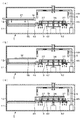
(第1の実施形態)
本発明の実施形態に係る現像装置1について、その縦断側面図、横断平面図である図1、図2を夫々参照しながら説明する。この現像装置1は筐体11を備えており、筺体11の側壁にはウエハWの搬送口12が開口している。この搬送口12を介して図2に示す搬送手段21によりウエハWが筐体11内に搬送される。
(First embodiment)
A developing device 1 according to an embodiment of the present invention will be described with reference to FIG. 1 and FIG. The developing device 1 includes a
例えばこのウエハWの表面には撥水性のレジスト膜が形成されており、このレジスト膜はポジレジストにより構成され、露光装置にて、所定のパターンに沿って露光されている。ただし、本発明の現像装置及び現像手法は、有機現像であっても適用することができ、ポジレジスト同様にネガレジストについても適用できる。有機現像とは有機物を主薬とする現像液を用いた現像である。また、ウエハWは、前記露光後この現像装置1に搬送するまでに加熱(ポストエクスポージャベーク:PEB)処理を受けている。搬送手段21は、ウエハWの側周を囲むアーム体22と、このアーム体22の側周に複数、この例では4つ設けられ、ウエハWの裏面を支持する支持部23とを備えている。
For example, a water-repellent resist film is formed on the surface of the wafer W, and the resist film is made of a positive resist and is exposed along a predetermined pattern by an exposure apparatus. However, the developing device and the developing method of the present invention can be applied even to organic development, and can be applied to a negative resist as well as a positive resist. Organic development is development using a developer containing an organic substance as a main agent. Further, the wafer W is subjected to a heating (post-exposure bake: PEB) process after the exposure and before being transferred to the developing device 1. The transfer means 21 includes an
筺体11内には、当該筐体11内を上下に仕切る仕切り板13が設けられている。仕切り板13の上側はウエハWを後述の処理容器5へ搬入するための搬入領域14aとして構成されている。搬入領域14aには冷却プレート15が設けられている。冷却プレート15は概ね円形に形成されており、前記搬送手段21との間でウエハWの受け渡しを行う際に、当該搬送手段21の支持部23と干渉しないように側周から中央に向かう切り欠き16が設けられている。冷却プレート15は、その裏面側に例えば温度調整された水を流すための図示しない流路を備えており、現像装置1の前段の加熱装置で加熱処理されたウエハWが冷却プレート15に載置されると、当該ウエハWが冷却される。
A
冷却プレート15にはスリット17a,17bが設けられ、後述の昇降ピン42がこのスリット17a、17bを介して冷却プレート15の表面上に突出する。仕切り板13の下側の下方領域14bには駆動部18が設けられており、搬送口12側から後述の温調プレート3側へ向けて形成されたガイド15aに沿って、冷却プレート15を水平方向に移動させる。
The cooling
現像装置1の斜視図である図3も参照しながら説明する。現像装置1の奥側にはウエハWを載置する円形の温調プレート3が設けられており、温調プレート3の内部には温調された流体、例えば水の流路31が形成されている。温調プレート3には温調水供給管32、温調水回収管33の各々の一端が接続されており、温調水供給管32、温調水回収管33の各々の他端はポンプ34に接続されている。温調水供給管32には温調部35が介設されており、当該温調部35に供給された水を加熱するためのヒータと、熱交換により前記水を冷却する冷媒の流路とを備えている。前記ヒータの出力及び前記冷媒の流通量が制御されることにより、ユーザが設定する温度に前記水が温調される。
The developing device 1 will be described with reference to FIG. 3 which is a perspective view. A circular
温調水供給管32、温調水回収管33及び流路31は温調水の循環路をなしており、ポンプ34により温調水供給管32に供給された水は、前記温調部35にて温調されて流路31に供給される。そして、ポンプ34により流路31から温調水回収管33を介して回収され、繰り返し温調水供給管32に供給されて温調される。このように温調水が流通することで、温調プレート3の表面全体の温度が均一に、且つ温調部35にて温調される水の温度と同じ温度に制御される。そして、温調プレート3に載置されたウエハWは、この温調プレート3表面と同じ温度に温調される。
The temperature adjustment
温調プレート3の表面の中央部に吸引口36が開口しており、温調プレート3の表面の周縁部には温調プレート3の周方向に沿って複数の吸引口37が開口している。これら吸引口36,37には排気管38の一端が各々接続されている。各排気管38の他端は合流し、流量制御部39を介して真空ポンプなどにより構成される排気手段40に接続されている。流量制御部39は、バルブやマスフローコントローラを備え、排気量を制御する。
A
温調プレート3の表面には、当該温調プレート3の周方向に3つの孔41が配列されており、この孔41には、温調プレート3の厚さ方向に3本の昇降ピン42が挿通されている(図1では便宜上2本のみ図示している)。昇降ピン42は、昇降機構43により温調プレート3の表面にて突没し、冷却プレート15と温調プレート3との間でウエハWの受け渡しを行う。温調プレート3内において、昇降ピン42の周囲には既述の温調水の漏れを防ぐためのシール部材44が設けられている。
Three
仕切り板13において、温調プレート3を囲うように複数の排気口45が開口しており、排気口45には排気管46の一端が接続されている。排気管46の他端は合流し、流量制御部47を介して排気手段40に接続されている。流量制御部47は、流量制御部39と同様に構成されている。また、仕切り板13上には排気口45を囲うようにOリング48が設けられている。
In the
温調プレート3上には処理容器5が設けられており、この処理容器5は、下方が開口した扁平な円形状の容器として構成されている。処理容器5は、支持部51を介して容器開閉機構をなす昇降機構52に接続され、当該昇降機構52により昇降自在に構成されている。図1に示すように処理容器5の下降時にはこの処理容器5の下端がOリング48に密着し、処理容器5内に気密な処理空間(処理雰囲気)Sが形成される。処理容器5の壁部には処理容器5の内壁を温調するヒータ59が設けられている。処理容器5の天井部の中央下面には霧状にした現像液を処理空間Sに供給するためのノズル53が設けられている。ノズル53は、処理容器5の天井中央部に設けられた開口部54を介して現像雰囲気ガス供給管55の一端に接続されている。
A
現像雰囲気ガス供給管55の他端は、現像雰囲気ガス加熱部56、流量制御部57をこの順に介して現像液が貯留された現像液供給源58に接続されている。現像液供給源58は不図示の圧送手段を備え、現像雰囲気ガス供給管55の下流側に現像液を供給する。流量制御部57は流量制御部39、47と同様にバルブやマスフローコントローラを備え、下流側への現像液の供給流量を制御する。現像雰囲気ガス加熱部56は、現像雰囲気ガス供給管55から供給された現像液と、後述の不活性ガス供給管61から供給されたN2ガスとを混合し、現像液のミスト(以下、現像ミストという)を含んだ現像雰囲気ガスを生成することができる。生成した現像雰囲気ガスは、現像雰囲気ガス供給管55を介して処理空間Sに供給される。さらに、現像雰囲気ガス加熱部56は例えばヒータなどの加熱手段を備えており、この現像雰囲気ガスを加熱し、所定の温度に調整することができる。
The other end of the developing atmosphere
例えば現像処理時に流量制御部57により現像雰囲気ガス加熱部56に供給される現像液の供給流量及び現像雰囲気ガスの温度はウエハWの処理ごとに一定となるように制御される。また、処理空間Sへの現像雰囲気ガスの供給時間もウエハW毎に一定になるように制御され、排気口45及び吸引口36、37からの排気量も例えばウエハWの処理ごとに一定となるように制御される。これによって、各ウエハWに一定の量の現像ミストが付着し、所定の厚さの現像液膜50が形成される。現像雰囲気ガス供給管55及び現像雰囲気ガス加熱部56は、雰囲気ガス供給部を構成する。
For example, the flow rate of the developing solution supplied to the developing atmosphere
この現像装置1では、処理空間Sへ現像雰囲気ガスの供給が開始されてから、予め設定された時間が経過したときに、現像液膜50を構成する液分が除去されてウエハW表面は乾燥した状態にされ、現像液とレジストとの反応が停止する。その後、ウエハWは現像装置1の外部に設けられた洗浄装置に搬送され、洗浄処理を受けて、レジストパターンが解像される。
In this developing apparatus 1, the liquid component constituting the
現像雰囲気ガス加熱部56には不活性ガス供給管61の一端が接続されている。不活性ガス供給管61の他端は、流量制御部63を介して不活性ガス例えばN2ガスが貯留されたN2ガス供給源64に接続されている。N2ガスは、上記のように現像雰囲気ガスに含まれた状態で、処理空間Sに供給することもできるし、パージガスとして、現像雰囲気ガス供給管55を介して単独で処理空間Sに供給することもできる。また、N2ガスはこのように単独で処理空間Sに供給される場合でも、現像雰囲気ガス加熱部56にて、例えば所定の温度に加熱されて供給される。
One end of an inert gas supply pipe 61 is connected to the developing atmosphere
この現像装置1は制御部100により、各部の動作が制御される。制御部100は、例えばコンピュータからなり、不図示のプログラム格納部を有している。このプログラム格納部には、後述の作用で説明する現像処理が行われるように命令が組まれた例えばソフトウエアからなるプログラムが格納されている。このプログラムが制御部100に読み出されることで、制御部100は現像装置1の各部へ制御信号を送信する。それによって、処理容器5及び昇降ピン42の昇降、温調部35による水の温調、温調プレート3の流路31への温調水の供給、処理容器5のヒータ59の出力、N2ガスや現像雰囲気ガスの処理空間Sへの供給などが制御される。このプログラムは、例えばハードディスク、コンパクトディスク、マグネットオプティカルディスクまたはメモリーカードなどの記憶媒体に収納された状態でプログラム格納部に格納される。
In the developing device 1, the operation of each unit is controlled by the
続いて、現像装置1の作用について図4〜図7を参照しながら説明する。また、図8には現像装置1及び前記洗浄装置による処理を受けて変化するウエハWの表面状態を示しており、この図8も適宜参照しながら説明する。温調プレート3の流路31には温調水が供給され、例えば温調プレート3表面が、予め設定された温度例えば20℃に温調される。また、排気口45及び吸引口36、37から所定の排気量で排気が行われると共にヒータ59により処理容器5の内壁の温度が、例えばウエハWに供給される現像雰囲気ガスの温度と同じ温度に温調される。
Next, the operation of the developing device 1 will be described with reference to FIGS. Further, FIG. 8 shows the surface state of the wafer W which is changed by the processing by the developing device 1 and the cleaning device, and will be described with reference to FIG. 8 as appropriate. Temperature control water is supplied to the
続いて、搬送手段21が、現像装置1の前段の加熱装置にて加熱処理されたウエハWを保持した状態で、搬送口12を介して筐体11内に進入し(図4(a))、下降してウエハWを冷却プレート15に受け渡した後に後退する(図4(b))。図8(a)はこのときのウエハWの表面を示しており、その表面のレジスト膜71は、露光部72と非露光部73とからなる。
Subsequently, the
冷却プレート15はウエハWを冷却しながら温調プレート3上へ前進する。冷却プレート15によりウエハWが温調プレート3上に搬送されると、昇降ピン42が上昇し、ウエハWを保持する(図4(c))。冷却プレート15が搬送口12側へ後退し(図5(a))、昇降ピン42が下降して、ウエハWが温調プレート3に載置される。ウエハWの中央部、周縁部が吸引口36、37に夫々吸引されて、ウエハWの裏面全体が温調プレート3表面に密着し、ウエハW全体が温調プレート3の表面温度と同じ温度になるように温調されると共に、処理容器5が下降して処理空間Sが形成される(図5(b))。
The cooling
現像雰囲気ガス加熱部56により現像ミストを含んだ現像雰囲気ガスが生成し、処理空間Sに供給され、前記現像ミストがウエハWに付着して、所定の膜厚の現像液膜50が形成されると(図5(c))、前記現像雰囲気ガスの供給と、排気口45からの排気とが停止し、現像液膜50とレジストとの反応が進行する(図6(a)、図8(b))。後に現像液膜50の除去を行うこと及び現像液の省液化の観点から、現像液膜の50膜厚H1が例えば1μm〜100μmになるように現像ミストの付着量が制御される。
A developing atmosphere gas containing a developing mist is generated by the developing atmosphere
処理空間Sへ前記現像雰囲気ガスの供給を開始してから予め設定された時間が経過したときに、排気口45からの排気が再び開始されると共に処理空間Sに所定の温度に加熱されたN2ガスが供給され(図6(b))、処理空間Sの現像雰囲気ガスがパージされて除去されると共にウエハWの表面がN2ガスにより乾燥された状態となる(図6(c)、図8(c))。その後、N2ガスの供給が停止し、昇降ピン42がウエハWを温調プレート3から浮かせると共に処理容器5が上昇して処理空間Sが外部雰囲気に開放される(図7(a))。
When a preset time has elapsed after the supply of the developing atmosphere gas to the processing space S is started, exhaust from the
然る後、冷却プレート15が温調プレート3上に移動し、当該ウエハWが冷却プレート15に載置され、冷却プレート15は搬送口12へと移動する(図7(b))。そして、冷却プレート15にウエハWを受け渡す時とは逆の動作で搬送手段21がウエハWを受け取り、ウエハWは洗浄装置に搬送される。この洗浄装置において、ウエハWに洗浄液70が供給され、図8(d)に示すように露光部72が、この洗浄液に押し流され、ウエハW表面から除去されて、レジストパターンが解像される。その後、洗浄液70が除去され、ウエハWが乾燥される(図8(e))。
Thereafter, the cooling
このように、この現像装置1では、ウエハWを温調プレート3に載置して、その表面に現像ミストを含む現像雰囲気ガスを供給して現像液膜50を形成し、現像雰囲気ガスの供給を開始してから予め設定された時間が経過したときに、N2ガスを処理空間Sに供給し、ウエハW表面を乾燥させている。これによって、現像液とレジストとの反応を停止させることができるので、前記反応が進行し過ぎることによるレジストパターンの劣化が抑えられる。従って、現像装置1の外部に設けられた洗浄装置にウエハWを搬送し、当該洗浄装置にて洗浄処理を行うことができるので、現像装置1にて一のウエハWを、洗浄装置にて他のウエハWを夫々並行して処理することができる。その結果として、スループットの向上を図ることができる。
As described above, in the developing device 1, the wafer W is placed on the
また、現像装置1は従来のように現像液を供給する装置ではないため、現像液を供給するためのノズルの移動機構や、ウエハWを保持した状態で回転させる回転機構などが不要である。従って、この実施形態のように現像液を供給する装置と洗浄液を供給する装置とを分けても、これらの装置を設置するスペースの大型化を抑えることができる。 Further, since the developing device 1 is not a device for supplying a developing solution as in the prior art, a nozzle moving mechanism for supplying the developing solution or a rotating mechanism for rotating the wafer W while holding it is unnecessary. Therefore, even if the apparatus for supplying the developer and the apparatus for supplying the cleaning liquid are separated as in this embodiment, the increase in the space for installing these apparatuses can be suppressed.
上記の第1の実施形態で、現像雰囲気ガスの供給を開始してから予め設定された時間が経過したときに、N2ガスを供給する代わりに、処理容器5を上昇させ、処理空間Sを外部雰囲気に開放してウエハWの乾燥を行ってもよい。処理空間Sが開放されると、処理容器5の外部の空気がウエハWの周囲に流れ、ウエハWの周囲の雰囲気に含まれる現像液の分圧が低下し、現像液膜50の蒸気圧が低下する。その結果、現像液膜50を構成する液分が蒸発して、ウエハW表面が乾燥した状態となる。また、ウエハWが乾燥された状態とは、現像液を構成する液分が除去された状態であり、現像液を構成する他の成分はウエハWに付着していてよい。前記液分を除去すれば現像液とレジストとの反応が停止することが、後述の評価試験で確認されている。
In the first embodiment, when a preset time has elapsed since the supply of the developing atmosphere gas has started, instead of supplying the N2 gas, the
(第2の実施形態)
ウエハW表面を乾燥した状態にする工程としては上記の例に限られない。以下、そのようにウエハW表面を乾燥状態にする各実施形態について説明する。図9には第2の実施形態の現像装置101の縦断側面図を示している。この現像装置101の現像装置1との差異点として、現像装置101では加熱部としてヒータ102を備えた載置プレートである冷却プレート103が設けられている。ヒータ102が設けられることを除いて、冷却プレート103は冷却プレート15と同様に構成される。この現像装置101では、処理空間Sが開放されてウエハWが乾燥された後、さらに冷却プレート103で加熱されることにより当該ウエハWの乾燥が行われ、現像液膜50の液分が除去される。
(Second Embodiment)
The process of making the surface of the wafer W dry is not limited to the above example. Hereinafter, each embodiment which makes the surface of the wafer W dry will be described. FIG. 9 shows a vertical side view of the developing
この現像装置101による処理手順について説明する。先ず、第1の実施形態と同様に冷却プレート103により、ウエハWが処理容器5に向けて搬送される。この処理容器5への搬送時において、例えばヒータ102の出力は低下しており、ウエハWは第1の実施形態と同様に冷却されながら、温調プレート3上へと搬送される。第1の実施形態と同様に現像液膜50の形成が行われると共に、ヒータ102の出力が上昇し、冷却プレート103の温度が上昇する(図10(a))。
A processing procedure by the developing
そして、温調プレート3にウエハWが載置されてから予め設定された時間が経過したときに、既述のように処理空間Sの外部雰囲気への開放が行われ、ウエハWの乾燥が進行する(図10(b))。そして、ウエハWが冷却プレート103に載置され、加熱されながら搬送口12へと搬送され、現像液膜50の液分が除去される(図10(c))。このような第2の実施形態においても第1の実施形態と同様の効果が得られる。
Then, when a preset time has elapsed since the wafer W was placed on the
また、第2の実施形態において、冷却プレート103の代わりに移動加熱プレートを設けてもよい。この移動加熱プレートは、例えばウエハWを冷却するための水の流路が設けられない他は、冷却プレート103と同様に構成される。そして、ウエハWを処理容器5へと搬送するときには当該ウエハWの冷却を行わず、ウエハWを温調プレート3から搬送口12へと搬送するときには、冷却プレート103と同様にウエハWを加熱する。
In the second embodiment, a moving heating plate may be provided instead of the
(第3の実施形態)
第3の実施形態では第1の実施形態の現像装置1が用いられる。第1の実施形態と同様にウエハWを温調プレート3に載置して、現像液膜50を形成する。そして、処理空間Sに現像雰囲気ガスを供給してから予め設定された時間が経過したときに、温調部35により温調プレート3の温度が、現像液の露点よりも高い温度、例えば沸点以上の温度に上昇する。それによって現像液膜50中の液分が蒸発して、ウエハWが乾燥状態とされる。その後は第1及び第2の実施形態と同様にウエハWが処理容器5から搬出される。
(Third embodiment)
In the third embodiment, the developing device 1 of the first embodiment is used. As in the first embodiment, the wafer W is placed on the
上記の各実施形態で、現像ミストの最大粒子径は例えば50μm以下であり、平均粒子径は例えば10μm以下である。このように粒子径を制御し、現像ミストをいわゆるドライフォグとすることで、現像処理を行う際にウエハW以外の箇所が現像液に濡れてしまうことを抑えることができる。それによって、現像欠陥やパーティクルの発生を抑えることができる。また、上記の現像雰囲気ガスの形成方法としては、現像液を加熱することに限られず、現像液に超音波を印加してもよい。 In each of the above embodiments, the maximum particle size of the developing mist is, for example, 50 μm or less, and the average particle size is, for example, 10 μm or less. By controlling the particle diameter and developing mist so-called dry fog in this way, it is possible to prevent the portions other than the wafer W from getting wet with the developer during the development process. Thereby, development defects and generation of particles can be suppressed. The method for forming the developing atmosphere gas is not limited to heating the developing solution, and an ultrasonic wave may be applied to the developing solution.
ところで、現像液膜50の形成手法としては、上記の例に限られない。例えば現像雰囲気ガス加熱部56において現像雰囲気ガスを、現像液の飽和温度よりも高い温度、例えば50℃に加熱し、現像液の蒸気(以下、現像蒸気と記載する)を生成する。そのように温度制御した現像雰囲気ガスを処理空間Sに供給すると共に温調プレート3によりウエハWを冷却して、前記現像蒸気をウエハW表面に結露させてもよい。この場合の現像装置1での処理工程について説明する。
By the way, the method of forming the
先ず、ヒータ59は処理容器5の内壁を、現像雰囲気ガスが結露しにくい温度に維持する。現像雰囲気ガスが結露しにくい温度とは、現像雰囲気ガスが結露しない温度も含み、処理空間Sに供給される現像雰囲気ガスに含まれる、現像液の蒸気の露点よりも高い温度のことを言う。そして、ウエハWが温調プレート3に載置されて、現像雰囲気ガスに含まれる現像蒸気の露点以下の温度に温調されると共に処理空間Sが形成される(図11(a))。処理空間Sに現像雰囲気ガスが供給され、前記現像蒸気がウエハW表面に結露し(図11(b))、所定の膜厚の現像液膜50が形成されると、現像雰囲気ガスの供給及び排気口45からの排気が停止する。その後、既述の第1の実施形態と同様にN2ガスが供給され、処理空間Sの現像雰囲気ガスが除去されると共にウエハWが乾燥される。
First, the
このように現像ミストを含まない現像雰囲気ガスをウエハWに供給する場合でも、既述の各実施形態と同様の効果が得られる。前記現像雰囲気ガスを供給する場合、処理空間S形成時には昇降ピン42がウエハWを浮いた状態で保持し、処理空間Sへ現像雰囲気ガスを供給した後にウエハWを温調プレート3に載置して現像液膜50を形成してもよい。処理中に温調プレート3に結露した現像液は吸引口36、37から吸引される。また、現像雰囲気ガスは、現像ミスト及び現像蒸気の両方を含んでいてもよく、その場合は現像ミストの付着分と現像蒸気の結露分とにより、現像液膜50が形成される。
Even when the developing atmosphere gas not containing the developing mist is supplied to the wafer W as described above, the same effects as those of the above-described embodiments can be obtained. When supplying the developing atmosphere gas, when the processing space S is formed, the lift pins 42 hold the wafer W in a floating state, and after supplying the developing atmosphere gas to the processing space S, the wafer W is placed on the
また、上記のように現像液を結露させて現像液膜50を形成する場合でもウエハWの乾燥は、他の実施形態の乾燥手法が適用でき、例えば処理空間Sを開放することにより行ってもよい。その他に例えば、昇降ピン42を介してウエハWを温調プレート3から浮き上がらせ、処理空間Sに残留している現像蒸気の熱により、ウエハWを乾燥させてもよい。各乾燥工程を開始するタイミングとしては、例えば現像液とレジストとの反応が終了した時点であり、つまり洗浄処理を行ったとした場合に不要なレジストを除去できる時点である。
Further, even when the
各実施形態において、処理容器5のヒータ59を設けることで、処理容器5へ現像液が付着してパーティクルとなることをより確実に防いでいるが、このようなヒータ59を設けなくてもよい。例えば現像雰囲気ガス加熱部56で加熱されたN2ガスを単独で処理空間Sに供給し、処理容器5の内壁を加熱する。それによって、前記内壁を、現像蒸気が結露する温度よりも高い温度に制御し、その後、上記の現像雰囲気ガスを供給してもよい。
In each embodiment, the provision of the
各実施形態に示したウエハWの乾燥手法は互いに組み合わせることができる。例えば第1の実施形態に第2の実施形態の冷却プレート103を適用し、N2ガス供給後、さらに冷却プレート103によりウエハWを加熱し、現像液膜50を除去してもよい。このように冷却プレートによる現像液膜50の除去を行わない場合、搬送手段21と昇降ピン42との間で直接ウエハWの受け渡しが行われてもよい。
The methods for drying the wafer W shown in the embodiments can be combined with each other. For example, the
(評価試験)
評価試験1
レジストが塗布され、所定のパターンに沿って露光されたウエハW1〜ウエハW3に夫々ノズルにより現像液を供給した。ウエハW1については現像液供給後のレジストの断面を撮像した。ウエハW2については現像液供給後に洗浄液を2秒供給した後、レジストの断面を撮像した。ウエハW3については現像液供給後に洗浄液を13秒供給した後、レジストの断面を撮像した。また、各ウエハW1〜W3に塗布するレジストの種類を変更して、同様の実験を行った。
(Evaluation test)
Evaluation test 1
A developing solution was supplied by a nozzle to each of the wafers W1 to W3 coated with a resist and exposed along a predetermined pattern. For the wafer W1, a cross section of the resist after supplying the developing solution was imaged. For the wafer W2, a cleaning solution was supplied for 2 seconds after supplying the developing solution, and then a cross section of the resist was imaged. For the wafer W3, the cleaning solution was supplied for 13 seconds after the developing solution was supplied, and then the cross section of the resist was imaged. In addition, the same experiment was performed by changing the type of resist applied to each of the wafers W1 to W3.
図12はこの評価試験1の結果を示している。図12(a)〜(c)が互いに同じレジストを用いたウエハW1〜W3の撮像結果であり、図12(d)〜(f)が互いに同じレジストを用いたウエハW1〜W3の撮像結果である。いずれのレジストを用いた場合であっても、洗浄液が供給されていないウエハW1についてはパターンの解像が進行していなかった。それに対して、洗浄液が供給されたウエハW2、W3についてはパターンが解像されていた。この実験の結果から露光されたレジストは、現像液が供給された段階ではなく、洗浄液が供給された段階で溶出を開始する。つまり、現像液により溶解された残渣を掻き出しているのではないことが分かる。従って、現像処理を行うにあたり、レジストに供給する現像液は少量であってもよいことが考えられる。この実験により本発明者は、上記の各実施形態のように、ウエハW表面に現像ミストを供給することで現像液の薄膜を形成することに思い至った。 FIG. 12 shows the results of this evaluation test 1. 12A to 12C show imaging results of the wafers W1 to W3 using the same resist, and FIGS. 12D to 12F show imaging results of the wafers W1 to W3 using the same resist. is there. Regardless of which resist is used, pattern resolution has not progressed for the wafer W1 to which no cleaning liquid is supplied. On the other hand, the patterns were resolved for the wafers W2 and W3 supplied with the cleaning liquid. As a result of this experiment, the exposed resist starts to elute not at the stage where the developer is supplied but at the stage where the cleaning liquid is supplied. That is, it is understood that the residue dissolved by the developer is not scraped out. Therefore, it is conceivable that a small amount of developer may be supplied to the resist when performing the development process. As a result of this experiment, the present inventor has come up with the idea that a thin film of developer is formed by supplying development mist to the surface of the wafer W as in the above embodiments.
評価試験2
評価試験1と同様に露光されたウエハW1、W2を用意した。ウエハW1についてはスピンチャックに載置し、そのスピンチャックにより鉛直軸回りに回転させながら、ノズルより現像液を供給した。現像液を供給しながら当該現像液の供給位置を、ウエハW1の周縁部から中心部に向けて径方向に移動させ、その後は中心部に向けて所定の時間現像液の供給を続けた。現像液供給後、ウエハW1に洗浄液を供給して現像液を除去し、レジストの断面を撮像した。
Evaluation test 2
Exposed wafers W1 and W2 were prepared in the same manner as in the evaluation test 1. The wafer W1 was placed on a spin chuck, and the developer was supplied from the nozzle while being rotated about the vertical axis by the spin chuck. While supplying the developing solution, the supply position of the developing solution was moved in the radial direction from the peripheral portion of the wafer W1 toward the central portion, and thereafter, the supply of the developing solution toward the central portion was continued for a predetermined time. After supplying the developing solution, a cleaning solution was supplied to the wafer W1 to remove the developing solution, and a cross section of the resist was imaged.
また、ウエハW2については容器本体と上蓋とからなる処理容器内に搬送した。上蓋を閉じて、処理容器内に気密な処理空間を形成した後、当該処理空間を排気しながら、第6の実施形態と同様に現像ミストを処理空間に供給して、処理雰囲気を形成した。現像ミスト供給後、ウエハW1に洗浄液を供給して現像液を除去し、レジストの断面を撮像した。 Further, the wafer W2 was transferred into a processing container including a container main body and an upper lid. After closing the upper lid and forming an airtight processing space in the processing container, a developing atmosphere was formed by supplying development mist to the processing space in the same manner as in the sixth embodiment while exhausting the processing space. After supplying the developing mist, a cleaning solution was supplied to the wafer W1 to remove the developing solution, and a cross section of the resist was imaged.
図13(a)(b)はウエハW1の撮像結果を、図13(c)(d)はウエハW2の撮像結果を、夫々示している。このようにウエハW1とW2とで形成されたパターンの形状に殆ど差が見られなかった。この実験からミスト状にした現像液を用いてもノズルから現像液を供給する場合と同様に現像を行うことができることが示された。 13A and 13B show the imaging results of the wafer W1, and FIGS. 13C and 13D show the imaging results of the wafer W2, respectively. Thus, there was almost no difference in the shape of the pattern formed by the wafers W1 and W2. From this experiment, it was shown that the development can be performed in the same manner as in the case where the developer is supplied from the nozzle even if the developer in the form of mist is used.
評価試験3
評価試験1、2と同様に露光されたウエハWを複数枚用意した。容器本体と上蓋とからなる処理容器に順次ウエハWを搬送し、上蓋を閉じて気密な処理空間を形成した後、処理空間を排気しながら、当該処理空間に前記現像ミストを供給して処理雰囲気を形成した。現像ミストの供給時間は45秒、60秒、90秒と夫々ウエハW毎に変更した。現像ミスト供給後は、上蓋を開いて処理空間を外部雰囲気に開放した後、ウエハWを取り出し、当該ウエハWに洗浄処理を行った。そして、各ウエハW面内の各所におけるレジストパターンのCDの平均を算出すると共にCDについて、ばらつきの指標である3σを算出した。現像ミストの供給時間が45秒、60秒、90秒である実験を、夫々評価試験3−1、3−2、3−3とする。
A plurality of exposed wafers W were prepared in the same manner as in the evaluation tests 1 and 2. After sequentially transferring the wafers W to a processing container composed of a container body and an upper lid, and closing the upper lid to form an airtight processing space, the developing mist is supplied to the processing space while exhausting the processing space, and a processing atmosphere Formed. The development mist supply time was changed to 45 seconds, 60 seconds, and 90 seconds for each wafer W, respectively. After supplying the developing mist, the upper lid was opened to open the processing space to the external atmosphere, and then the wafer W was taken out and subjected to a cleaning process. Then, the average of the CD of the resist pattern at each location within each wafer W surface was calculated, and 3σ, which is an index of variation, was calculated for the CD. The experiments in which the development mist supply time is 45 seconds, 60 seconds, and 90 seconds are referred to as evaluation tests 3-1, 3-2, and 3-3, respectively.
評価試験4
評価試験2と同様にノズルから現像液を供給し、洗浄処理を行ったウエハWについても評価試験4と同様にCDの平均及び3σを算出した。ノズルからの現像液の供給時間は、ウエハWごとに変更した。この供給時間が短い順に夫々評価試験4−1、4−2、4−3とする。
Evaluation test 4
Similarly to the evaluation test 2, the average value of CD and 3σ were also calculated for the wafer W which was supplied with the developer from the nozzle and was subjected to the cleaning process as in the evaluation test 4. The supply time of the developer from the nozzle was changed for each wafer W. Evaluation tests 4-1, 4-2, and 4-3 are respectively performed in order of decreasing supply time.
評価試験5
ウエハWの径方向に伸びる吐出口を備えたノズルをウエハWの一端側から他端側へ、現像液を吐出しながら移動させてウエハWに液盛りを行った後、洗浄処理を行った。現像液の供給時間はウエハW毎に変更しており、この供給時間が30秒、60秒であるものを夫々評価試験5−1、5−2とする。
A nozzle provided with a discharge port extending in the radial direction of the wafer W was moved from one end side to the other end side of the wafer W while discharging the developer to fill the wafer W, and then a cleaning process was performed. The supply time of the developer is changed for each wafer W, and those having a supply time of 30 seconds and 60 seconds are referred to as evaluation tests 5-1 and 5-2, respectively.
図14は評価試験3〜5の結果を示している。図中の棒グラフが各評価試験のCD平均を、図中の点が各評価試験の3σを夫々示している。この結果から、現像ミストとして現像液を供給する場合も、ノズルにより現像液を供給する場合と同様に現像液の供給時間が長くなるとCD平均が小さくなっていくことが分かる。また、3σについては、現像ミストとして現像液を供給する場合と、ノズルにより現像液を供給する場合との間で大きな差はない。これらの評価試験の結果から現像ミストによる現像は、ノズルにより現像液を供給する現像に比べてパターン形状に大きな影響を与えないことが示された。
FIG. 14 shows the results of
評価試験6
評価試験3と同様に、露光されたウエハWが搬入された処理空間を排気しながら、当該処理空間に現像ミストを供給した。現像ミストの供給時間は30秒とした。現像ミストの供給停止後、処理空間を外部雰囲気に開放してウエハW表面を乾燥させ、その後にウエハWの洗浄処理を行った。そして、評価試験3と同様にレジストパターンのCDの平均とCDの3σを算出した。現像ミストの供給停止から処理空間の開放までの時間はウエハW毎に設定し、夫々30秒、180秒とした。この開放までの時間が30秒であるものを評価試験6−1とし、180秒であるものを6−2とする。
Similarly to the
また、現像ミストの供給時間を60秒にして評価試験6−1、6−2と同様の実験を行った。現像ミストの供給停止から前記処理空間の開放までの時間はウエハW毎に変更し、夫々0秒、30秒、180秒とした。この開放までの時間が0秒、30秒、180秒であるものを夫々6−3、6−4、6−5とする。 Further, an experiment similar to the evaluation tests 6-1 and 6-2 was performed with a developing mist supply time of 60 seconds. The time from the stop of the supply of the developing mist to the opening of the processing space was changed for each wafer W, and was set to 0 seconds, 30 seconds, and 180 seconds, respectively. The time until the opening is 0 seconds, 30 seconds, and 180 seconds is defined as 6-3, 6-4, and 6-5, respectively.
図15は評価試験6の結果を示している。図中の棒グラフがCDの平均を、図中の点がCDの3σを夫々示している。評価試験6−5では評価試験6−1〜6−4に比べて3σが若干大きくなっている。つまり、評価試験6−5ではパターンのCDのばらつきが若干大きくなっている。また、処理空間を開放するまでの時間が長くなるにつれて、CDの平均が小さくなっている。これは現像ミストの供給を停止しても、処理空間に残った現像ミストによりウエハW表面が乾燥せず、現像が進んだためであると考えられる。この評価試験6の結果から、パターン形状は、ウエハW表面が乾燥するまでの時間により影響されることが分かる。
FIG. 15 shows the result of the
評価試験7
評価試験3と同様に、露光されたウエハWが搬入された処理空間を排気しながら、当該処理空間に現像ミストを供給した。現像ミストの供給時間は60秒とした。現像ミストの供給停止後、処理空間を開放してウエハW表面を乾燥させ、その後にウエハWの洗浄処理を行った。処理空間を開放してから洗浄処理を行うまでの時間はウエハW毎に設定し、夫々10秒、45秒、90秒、180秒、600秒とした。洗浄処理後は、評価試験3と同様にレジストパターンのCDの平均とCDの3σを算出した。洗浄処理を行うまでの時間が10秒、45秒、90秒、180秒、600秒であるものを夫々評価試験7−1、7−2、7−3、7−4、7−5とする。
Evaluation test 7
Similarly to the
図16は評価試験7の結果を示している。図中の棒グラフがCDの平均を、図中の点がCDの3σを夫々示している。各評価試験間でCDの平均及び3σは大きく変動していない。従って、ウエハWの乾燥を行ってから洗浄処理を行うまでの時間はパターンの形状に大きく影響しないことが分かる。従って、上記のようにウエハW表面を乾燥させた後、洗浄装置までウエハWを搬送して洗浄処理を行うことが可能であることが確認された。 FIG. 16 shows the result of the evaluation test 7. The bar graph in the figure shows the average of CD, and the point in the figure shows 3σ of CD. The CD average and 3σ do not vary greatly between the evaluation tests. Therefore, it can be seen that the time from the drying of the wafer W to the cleaning process does not significantly affect the pattern shape. Accordingly, it has been confirmed that after the surface of the wafer W is dried as described above, the wafer W can be transported to the cleaning apparatus to perform the cleaning process.
W ウエハ
S 処理空間
1 現像装置
11 筐体
12 搬送口
15 冷却プレート
21 搬送手段
3 温調プレート
35 温調部
36、37 吸引口
42 昇降ピン
43 昇降機構
45 排気口
5 処理容器
56 現像雰囲気ガス加熱部
100 制御部
W Wafer S Processing space 1
Claims (15)
処理雰囲気を形成する気密な処理容器と、
この処理容器内に搬入された基板の表面に現像液の液膜を形成するために、当該処理容器内に現像液のミストを供給する雰囲気ガス供給部と、
処理容器内の処理雰囲気を外部雰囲気に開放するための容器開閉機構により構成され、前記液膜による現像を停止するために基板を乾燥する乾燥部と、
を備えていることを特徴とする現像装置。 In a developing device for developing an exposed substrate,
An airtight processing vessel forming a processing atmosphere;
In order to form a liquid film of the developer on the surface of the substrate carried into the processing container, an atmospheric gas supply unit that supplies a mist of the developing solution into the processing container;
A drying unit configured to open a processing atmosphere in the processing container to an external atmosphere, and drying the substrate to stop development by the liquid film;
A developing device comprising:
処理雰囲気を形成する気密な処理容器内に基板を搬入する工程と、
次いで処理容器内に現像液のミストを供給し、基板の表面に現像液の液膜を形成する液膜形成工程と、
前記液膜による現像を停止するために基板を乾燥する乾燥工程と、
を含み、
前記乾燥工程は、処理容器内の処理雰囲気を外部雰囲気に開放する工程を含むことを特徴とする現像方法。 In a developing method for developing an exposed substrate,
A step of carrying the substrate into an airtight processing container forming a processing atmosphere;
Next, a liquid film forming step of supplying a mist of the developer into the processing container and forming a liquid film of the developer on the surface of the substrate;
A drying step of drying the substrate to stop development with the liquid film;
Including
The developing method , wherein the drying step includes a step of opening a processing atmosphere in the processing container to an external atmosphere .
基板表面に前記蒸気が結露するように基板の温度を制御する工程を含むことを特徴とする請求項8ないし11のいずれか一つに記載の現像方法。 Instead of supplying a developer mist to form a developer film on the surface of the substrate, the developer is condensed in the processing container to form a liquid film by dewing the developer on the surface of the substrate. Supplying a gas containing the vapor of
Developing method according to any one of claims 8 to 11, comprising the step of controlling the temperature of the substrate such that the vapor on the substrate surface condensation.
前記プログラムは、請求項8ないし14のいずれか一項に記載の現像方法を実行するようにステップ群が組まれていることを特徴とする記憶媒体。 In a storage medium storing a program used in a developing device that develops an exposed substrate in a processing container,
The program, storage medium, wherein the step group is organized to perform a developing method according to any one of claims 8 to 14.
Priority Applications (5)
| Application Number | Priority Date | Filing Date | Title |
|---|---|---|---|
| JP2010030524A JP5003773B2 (en) | 2010-02-15 | 2010-02-15 | Developing device, developing method, and storage medium |
| TW099144777A TWI393173B (en) | 2010-02-15 | 2010-12-20 | Developing apparatus, developing method and storage medium |
| US13/025,490 US8333522B2 (en) | 2010-02-15 | 2011-02-11 | Developing apparatus, developing method and storage medium |
| KR1020110012370A KR101185072B1 (en) | 2010-02-15 | 2011-02-11 | Developing apparatus, developing method and storage medium |
| CN201110039009.XA CN102163009B (en) | 2010-02-15 | 2011-02-15 | Developing apparatus and developing method |
Applications Claiming Priority (1)
| Application Number | Priority Date | Filing Date | Title |
|---|---|---|---|
| JP2010030524A JP5003773B2 (en) | 2010-02-15 | 2010-02-15 | Developing device, developing method, and storage medium |
Publications (2)
| Publication Number | Publication Date |
|---|---|
| JP2011166086A JP2011166086A (en) | 2011-08-25 |
| JP5003773B2 true JP5003773B2 (en) | 2012-08-15 |
Family
ID=44369886
Family Applications (1)
| Application Number | Title | Priority Date | Filing Date |
|---|---|---|---|
| JP2010030524A Active JP5003773B2 (en) | 2010-02-15 | 2010-02-15 | Developing device, developing method, and storage medium |
Country Status (5)
| Country | Link |
|---|---|
| US (1) | US8333522B2 (en) |
| JP (1) | JP5003773B2 (en) |
| KR (1) | KR101185072B1 (en) |
| CN (1) | CN102163009B (en) |
| TW (1) | TWI393173B (en) |
Families Citing this family (16)
| Publication number | Priority date | Publication date | Assignee | Title |
|---|---|---|---|---|
| JP5003774B2 (en) | 2010-02-15 | 2012-08-15 | 東京エレクトロン株式会社 | Developing device, developing method, and storage medium |
| JP5067432B2 (en) * | 2010-02-15 | 2012-11-07 | 東京エレクトロン株式会社 | Coating, developing device, developing method, and storage medium |
| US20140273290A1 (en) * | 2013-03-15 | 2014-09-18 | Tokyo Electron Limited | Solvent anneal processing for directed-self assembly applications |
| KR102394994B1 (en) | 2013-09-04 | 2022-05-04 | 도쿄엘렉트론가부시키가이샤 | Uv-assisted stripping of hardened photoresist to create chemical templates for directed self-assembly |
| US9349604B2 (en) | 2013-10-20 | 2016-05-24 | Tokyo Electron Limited | Use of topography to direct assembly of block copolymers in grapho-epitaxial applications |
| US9793137B2 (en) | 2013-10-20 | 2017-10-17 | Tokyo Electron Limited | Use of grapho-epitaxial directed self-assembly applications to precisely cut logic lines |
| CN104714376B (en) * | 2015-04-02 | 2018-09-18 | 合肥鑫晟光电科技有限公司 | A kind of developing apparatus and developing method |
| US9947597B2 (en) | 2016-03-31 | 2018-04-17 | Tokyo Electron Limited | Defectivity metrology during DSA patterning |
| CN107065453A (en) * | 2017-02-14 | 2017-08-18 | 京东方科技集团股份有限公司 | Dry component and developing apparatus |
| JP6981092B2 (en) * | 2017-08-10 | 2021-12-15 | 東京エレクトロン株式会社 | Liquid treatment equipment |
| CN113227909A (en) | 2018-12-20 | 2021-08-06 | 朗姆研究公司 | Dry development of resists |
| TWI837391B (en) | 2019-06-26 | 2024-04-01 | 美商蘭姆研究公司 | Photoresist development with halide chemistries |
| KR102431292B1 (en) | 2020-01-15 | 2022-08-09 | 램 리써치 코포레이션 | Bottom layer for photoresist adhesion and dose reduction |
| KR102601038B1 (en) | 2020-07-07 | 2023-11-09 | 램 리써치 코포레이션 | Integrated dry processes for patterning radiation photoresist patterning |
| CN115598943A (en) * | 2020-11-13 | 2023-01-13 | 朗姆研究公司(Us) | Processing tool for dry removal of photoresist |
| CN114236979A (en) * | 2021-12-15 | 2022-03-25 | 江苏集萃微纳自动化系统与装备技术研究所有限公司 | Nanostructure developing device, developing method and application |
Family Cites Families (15)
| Publication number | Priority date | Publication date | Assignee | Title |
|---|---|---|---|---|
| JPS57208135A (en) * | 1981-06-18 | 1982-12-21 | Fujitsu Ltd | Spray type resist developing apparatus |
| JPH07326559A (en) * | 1994-05-31 | 1995-12-12 | Oki Electric Ind Co Ltd | Resist developing device |
| US5853961A (en) * | 1995-04-19 | 1998-12-29 | Tokyo Electron Limited | Method of processing substrate and apparatus for processing substrate |
| JP4148388B2 (en) * | 2001-07-24 | 2008-09-10 | 東京エレクトロン株式会社 | Heat treatment equipment |
| JP3989221B2 (en) * | 2001-10-25 | 2007-10-10 | 東京エレクトロン株式会社 | Heat treatment apparatus and heat treatment method |
| US6955485B2 (en) * | 2002-03-01 | 2005-10-18 | Tokyo Electron Limited | Developing method and developing unit |
| JP4275488B2 (en) * | 2002-10-28 | 2009-06-10 | 大日本スクリーン製造株式会社 | Substrate processing apparatus and substrate processing method |
| CN100424822C (en) * | 2003-06-06 | 2008-10-08 | 东京毅力科创株式会社 | Method for improving surface roughness of processed film of substrate and apparatus for processing substrate |
| JP4369325B2 (en) * | 2003-12-26 | 2009-11-18 | 東京エレクトロン株式会社 | Development device and development processing method |
| JP2005277268A (en) * | 2004-03-26 | 2005-10-06 | Dainippon Screen Mfg Co Ltd | Substrate treatment apparatus and substrate treatment method |
| US7135267B2 (en) * | 2004-08-06 | 2006-11-14 | E. I. Du Pont De Nemours And Company | Aqueous developable photoimageable compositions for use in photo-patterning methods |
| JP4318709B2 (en) * | 2006-10-10 | 2009-08-26 | 東京エレクトロン株式会社 | Development processing method and development processing apparatus |
| JP2008300876A (en) * | 2008-09-01 | 2008-12-11 | Toshiba Corp | Method for processing substrate |
| JP5003774B2 (en) * | 2010-02-15 | 2012-08-15 | 東京エレクトロン株式会社 | Developing device, developing method, and storage medium |
| JP5067432B2 (en) * | 2010-02-15 | 2012-11-07 | 東京エレクトロン株式会社 | Coating, developing device, developing method, and storage medium |
-
2010
- 2010-02-15 JP JP2010030524A patent/JP5003773B2/en active Active
- 2010-12-20 TW TW099144777A patent/TWI393173B/en active
-
2011
- 2011-02-11 KR KR1020110012370A patent/KR101185072B1/en not_active IP Right Cessation
- 2011-02-11 US US13/025,490 patent/US8333522B2/en active Active
- 2011-02-15 CN CN201110039009.XA patent/CN102163009B/en not_active Expired - Fee Related
Also Published As
| Publication number | Publication date |
|---|---|
| KR101185072B1 (en) | 2012-09-21 |
| CN102163009B (en) | 2013-03-27 |
| CN102163009A (en) | 2011-08-24 |
| US8333522B2 (en) | 2012-12-18 |
| JP2011166086A (en) | 2011-08-25 |
| TW201207895A (en) | 2012-02-16 |
| US20110200953A1 (en) | 2011-08-18 |
| TWI393173B (en) | 2013-04-11 |
| KR20110094246A (en) | 2011-08-23 |
Similar Documents
| Publication | Publication Date | Title |
|---|---|---|
| JP5003773B2 (en) | Developing device, developing method, and storage medium | |
| JP5003774B2 (en) | Developing device, developing method, and storage medium | |
| JP5067432B2 (en) | Coating, developing device, developing method, and storage medium | |
| KR102753390B1 (en) | Heat treatment method and heat treatment apparatus | |
| JP4853536B2 (en) | Coating, developing device, coating, developing method and storage medium | |
| JP5303954B2 (en) | Hydrophobic treatment method, hydrophobic treatment device, coating, developing device and storage medium | |
| JP5099054B2 (en) | Substrate processing apparatus, substrate processing method, coating and developing apparatus, coating and developing method, and storage medium | |
| JP4975790B2 (en) | Resist solution supply apparatus, resist solution supply method, program, and computer storage medium | |
| JP4654119B2 (en) | Coating / developing apparatus and coating / developing method | |
| JP5584176B2 (en) | Development processing apparatus, development processing method, program, and computer storage medium | |
| TWI814298B (en) | Substrate drying device and substrate processing device | |
| JP5065121B2 (en) | Resist solution supply apparatus, resist solution supply method, program, and computer storage medium | |
| JP7158549B2 (en) | SUBSTRATE PROCESSING METHOD, SUBSTRATE PROCESSING SYSTEM AND COMPUTER-READABLE STORAGE MEDIUM | |
| KR102567503B1 (en) | Apparatus and method for treating substrate | |
| JP2011049353A (en) | Application film forming method, program, computer storage medium, and substrate processing system |
Legal Events
| Date | Code | Title | Description |
|---|---|---|---|
| A621 | Written request for application examination |
Free format text: JAPANESE INTERMEDIATE CODE: A621 Effective date: 20111124 |
|
| A131 | Notification of reasons for refusal |
Free format text: JAPANESE INTERMEDIATE CODE: A131 Effective date: 20120131 |
|
| A521 | Request for written amendment filed |
Free format text: JAPANESE INTERMEDIATE CODE: A523 Effective date: 20120402 |
|
| TRDD | Decision of grant or rejection written | ||
| A01 | Written decision to grant a patent or to grant a registration (utility model) |
Free format text: JAPANESE INTERMEDIATE CODE: A01 Effective date: 20120424 |
|
| A01 | Written decision to grant a patent or to grant a registration (utility model) |
Free format text: JAPANESE INTERMEDIATE CODE: A01 |
|
| A61 | First payment of annual fees (during grant procedure) |
Free format text: JAPANESE INTERMEDIATE CODE: A61 Effective date: 20120507 |
|
| FPAY | Renewal fee payment (event date is renewal date of database) |
Free format text: PAYMENT UNTIL: 20150601 Year of fee payment: 3 |
|
| R150 | Certificate of patent or registration of utility model |
Ref document number: 5003773 Country of ref document: JP Free format text: JAPANESE INTERMEDIATE CODE: R150 Free format text: JAPANESE INTERMEDIATE CODE: R150 |
|
| R250 | Receipt of annual fees |
Free format text: JAPANESE INTERMEDIATE CODE: R250 |
|
| R250 | Receipt of annual fees |
Free format text: JAPANESE INTERMEDIATE CODE: R250 |
|
| R250 | Receipt of annual fees |
Free format text: JAPANESE INTERMEDIATE CODE: R250 |
|
| R250 | Receipt of annual fees |
Free format text: JAPANESE INTERMEDIATE CODE: R250 |
|
| R250 | Receipt of annual fees |
Free format text: JAPANESE INTERMEDIATE CODE: R250 |
|
| R250 | Receipt of annual fees |
Free format text: JAPANESE INTERMEDIATE CODE: R250 |