JP5000877B2 - Semiconductor device - Google Patents
Semiconductor device Download PDFInfo
- Publication number
- JP5000877B2 JP5000877B2 JP2005294940A JP2005294940A JP5000877B2 JP 5000877 B2 JP5000877 B2 JP 5000877B2 JP 2005294940 A JP2005294940 A JP 2005294940A JP 2005294940 A JP2005294940 A JP 2005294940A JP 5000877 B2 JP5000877 B2 JP 5000877B2
- Authority
- JP
- Japan
- Prior art keywords
- semiconductor device
- conductor pattern
- film
- external electrode
- insulating layer
- Prior art date
- Legal status (The legal status is an assumption and is not a legal conclusion. Google has not performed a legal analysis and makes no representation as to the accuracy of the status listed.)
- Active
Links
- 239000004065 semiconductor Substances 0.000 title claims description 83
- 239000002184 metal Substances 0.000 claims description 76
- 229910052751 metal Inorganic materials 0.000 claims description 76
- 239000011347 resin Substances 0.000 claims description 61
- 229920005989 resin Polymers 0.000 claims description 61
- 239000004020 conductor Substances 0.000 claims description 21
- 229910000679 solder Inorganic materials 0.000 description 14
- 238000000034 method Methods 0.000 description 12
- 238000007789 sealing Methods 0.000 description 10
- 238000004519 manufacturing process Methods 0.000 description 7
- 230000004048 modification Effects 0.000 description 5
- 238000012986 modification Methods 0.000 description 5
- 230000000694 effects Effects 0.000 description 4
- 229920002120 photoresistant polymer Polymers 0.000 description 3
- XUIMIQQOPSSXEZ-UHFFFAOYSA-N Silicon Chemical compound [Si] XUIMIQQOPSSXEZ-UHFFFAOYSA-N 0.000 description 2
- 238000000059 patterning Methods 0.000 description 2
- 238000007747 plating Methods 0.000 description 2
- 229920001721 polyimide Polymers 0.000 description 2
- 239000009719 polyimide resin Substances 0.000 description 2
- 229910052710 silicon Inorganic materials 0.000 description 2
- 239000010703 silicon Substances 0.000 description 2
- 238000004544 sputter deposition Methods 0.000 description 2
- 230000035882 stress Effects 0.000 description 2
- 239000000654 additive Substances 0.000 description 1
- 229910045601 alloy Inorganic materials 0.000 description 1
- 239000000956 alloy Substances 0.000 description 1
- 230000004888 barrier function Effects 0.000 description 1
- 229910052802 copper Inorganic materials 0.000 description 1
- 238000010586 diagram Methods 0.000 description 1
- 238000005530 etching Methods 0.000 description 1
- 238000005304 joining Methods 0.000 description 1
- 230000000149 penetrating effect Effects 0.000 description 1
- 238000004382 potting Methods 0.000 description 1
- 238000001556 precipitation Methods 0.000 description 1
- 239000000758 substrate Substances 0.000 description 1
- 230000008646 thermal stress Effects 0.000 description 1
- 238000001721 transfer moulding Methods 0.000 description 1
Images


Classifications
-
- H—ELECTRICITY
- H01—ELECTRIC ELEMENTS
- H01L—SEMICONDUCTOR DEVICES NOT COVERED BY CLASS H10
- H01L21/00—Processes or apparatus adapted for the manufacture or treatment of semiconductor or solid state devices or of parts thereof
- H01L21/67—Apparatus specially adapted for handling semiconductor or electric solid state devices during manufacture or treatment thereof; Apparatus specially adapted for handling wafers during manufacture or treatment of semiconductor or electric solid state devices or components ; Apparatus not specifically provided for elsewhere
- H01L21/683—Apparatus specially adapted for handling semiconductor or electric solid state devices during manufacture or treatment thereof; Apparatus specially adapted for handling wafers during manufacture or treatment of semiconductor or electric solid state devices or components ; Apparatus not specifically provided for elsewhere for supporting or gripping
- H01L21/6835—Apparatus specially adapted for handling semiconductor or electric solid state devices during manufacture or treatment thereof; Apparatus specially adapted for handling wafers during manufacture or treatment of semiconductor or electric solid state devices or components ; Apparatus not specifically provided for elsewhere for supporting or gripping using temporarily an auxiliary support
-
- H—ELECTRICITY
- H01—ELECTRIC ELEMENTS
- H01L—SEMICONDUCTOR DEVICES NOT COVERED BY CLASS H10
- H01L21/00—Processes or apparatus adapted for the manufacture or treatment of semiconductor or solid state devices or of parts thereof
- H01L21/02—Manufacture or treatment of semiconductor devices or of parts thereof
- H01L21/04—Manufacture or treatment of semiconductor devices or of parts thereof the devices having potential barriers, e.g. a PN junction, depletion layer or carrier concentration layer
- H01L21/50—Assembly of semiconductor devices using processes or apparatus not provided for in a single one of the groups H01L21/18 - H01L21/326 or H10D48/04 - H10D48/07 e.g. sealing of a cap to a base of a container
- H01L21/56—Encapsulations, e.g. encapsulation layers, coatings
- H01L21/563—Encapsulation of active face of flip-chip device, e.g. underfilling or underencapsulation of flip-chip, encapsulation preform on chip or mounting substrate
-
- H—ELECTRICITY
- H01—ELECTRIC ELEMENTS
- H01L—SEMICONDUCTOR DEVICES NOT COVERED BY CLASS H10
- H01L21/00—Processes or apparatus adapted for the manufacture or treatment of semiconductor or solid state devices or of parts thereof
- H01L21/02—Manufacture or treatment of semiconductor devices or of parts thereof
- H01L21/04—Manufacture or treatment of semiconductor devices or of parts thereof the devices having potential barriers, e.g. a PN junction, depletion layer or carrier concentration layer
- H01L21/50—Assembly of semiconductor devices using processes or apparatus not provided for in a single one of the groups H01L21/18 - H01L21/326 or H10D48/04 - H10D48/07 e.g. sealing of a cap to a base of a container
- H01L21/56—Encapsulations, e.g. encapsulation layers, coatings
- H01L21/568—Temporary substrate used as encapsulation process aid
-
- H—ELECTRICITY
- H01—ELECTRIC ELEMENTS
- H01L—SEMICONDUCTOR DEVICES NOT COVERED BY CLASS H10
- H01L23/00—Details of semiconductor or other solid state devices
- H01L23/28—Encapsulations, e.g. encapsulating layers, coatings, e.g. for protection
- H01L23/31—Encapsulations, e.g. encapsulating layers, coatings, e.g. for protection characterised by the arrangement or shape
- H01L23/3107—Encapsulations, e.g. encapsulating layers, coatings, e.g. for protection characterised by the arrangement or shape the device being completely enclosed
- H01L23/3121—Encapsulations, e.g. encapsulating layers, coatings, e.g. for protection characterised by the arrangement or shape the device being completely enclosed a substrate forming part of the encapsulation
- H01L23/3128—Encapsulations, e.g. encapsulating layers, coatings, e.g. for protection characterised by the arrangement or shape the device being completely enclosed a substrate forming part of the encapsulation the substrate having spherical bumps for external connection
-
- H—ELECTRICITY
- H01—ELECTRIC ELEMENTS
- H01L—SEMICONDUCTOR DEVICES NOT COVERED BY CLASS H10
- H01L23/00—Details of semiconductor or other solid state devices
- H01L23/28—Encapsulations, e.g. encapsulating layers, coatings, e.g. for protection
- H01L23/31—Encapsulations, e.g. encapsulating layers, coatings, e.g. for protection characterised by the arrangement or shape
- H01L23/3107—Encapsulations, e.g. encapsulating layers, coatings, e.g. for protection characterised by the arrangement or shape the device being completely enclosed
- H01L23/3142—Sealing arrangements between parts, e.g. adhesion promotors
-
- H—ELECTRICITY
- H01—ELECTRIC ELEMENTS
- H01L—SEMICONDUCTOR DEVICES NOT COVERED BY CLASS H10
- H01L23/00—Details of semiconductor or other solid state devices
- H01L23/48—Arrangements for conducting electric current to or from the solid state body in operation, e.g. leads, terminal arrangements ; Selection of materials therefor
- H01L23/488—Arrangements for conducting electric current to or from the solid state body in operation, e.g. leads, terminal arrangements ; Selection of materials therefor consisting of soldered or bonded constructions
- H01L23/498—Leads, i.e. metallisations or lead-frames on insulating substrates, e.g. chip carriers
- H01L23/49811—Additional leads joined to the metallisation on the insulating substrate, e.g. pins, bumps, wires, flat leads
- H01L23/49816—Spherical bumps on the substrate for external connection, e.g. ball grid arrays [BGA]
-
- H—ELECTRICITY
- H01—ELECTRIC ELEMENTS
- H01L—SEMICONDUCTOR DEVICES NOT COVERED BY CLASS H10
- H01L23/00—Details of semiconductor or other solid state devices
- H01L23/48—Arrangements for conducting electric current to or from the solid state body in operation, e.g. leads, terminal arrangements ; Selection of materials therefor
- H01L23/488—Arrangements for conducting electric current to or from the solid state body in operation, e.g. leads, terminal arrangements ; Selection of materials therefor consisting of soldered or bonded constructions
- H01L23/498—Leads, i.e. metallisations or lead-frames on insulating substrates, e.g. chip carriers
- H01L23/49838—Geometry or layout
-
- H—ELECTRICITY
- H01—ELECTRIC ELEMENTS
- H01L—SEMICONDUCTOR DEVICES NOT COVERED BY CLASS H10
- H01L24/00—Arrangements for connecting or disconnecting semiconductor or solid-state bodies; Methods or apparatus related thereto
- H01L24/01—Means for bonding being attached to, or being formed on, the surface to be connected, e.g. chip-to-package, die-attach, "first-level" interconnects; Manufacturing methods related thereto
- H01L24/26—Layer connectors, e.g. plate connectors, solder or adhesive layers; Manufacturing methods related thereto
- H01L24/31—Structure, shape, material or disposition of the layer connectors after the connecting process
- H01L24/32—Structure, shape, material or disposition of the layer connectors after the connecting process of an individual layer connector
-
- H—ELECTRICITY
- H01—ELECTRIC ELEMENTS
- H01L—SEMICONDUCTOR DEVICES NOT COVERED BY CLASS H10
- H01L2221/00—Processes or apparatus adapted for the manufacture or treatment of semiconductor or solid state devices or of parts thereof covered by H01L21/00
- H01L2221/67—Apparatus for handling semiconductor or electric solid state devices during manufacture or treatment thereof; Apparatus for handling wafers during manufacture or treatment of semiconductor or electric solid state devices or components; Apparatus not specifically provided for elsewhere
- H01L2221/683—Apparatus for handling semiconductor or electric solid state devices during manufacture or treatment thereof; Apparatus for handling wafers during manufacture or treatment of semiconductor or electric solid state devices or components; Apparatus not specifically provided for elsewhere for supporting or gripping
- H01L2221/68304—Apparatus for handling semiconductor or electric solid state devices during manufacture or treatment thereof; Apparatus for handling wafers during manufacture or treatment of semiconductor or electric solid state devices or components; Apparatus not specifically provided for elsewhere for supporting or gripping using temporarily an auxiliary support
- H01L2221/68345—Apparatus for handling semiconductor or electric solid state devices during manufacture or treatment thereof; Apparatus for handling wafers during manufacture or treatment of semiconductor or electric solid state devices or components; Apparatus not specifically provided for elsewhere for supporting or gripping using temporarily an auxiliary support used as a support during the manufacture of self supporting substrates
-
- H—ELECTRICITY
- H01—ELECTRIC ELEMENTS
- H01L—SEMICONDUCTOR DEVICES NOT COVERED BY CLASS H10
- H01L2224/00—Indexing scheme for arrangements for connecting or disconnecting semiconductor or solid-state bodies and methods related thereto as covered by H01L24/00
- H01L2224/01—Means for bonding being attached to, or being formed on, the surface to be connected, e.g. chip-to-package, die-attach, "first-level" interconnects; Manufacturing methods related thereto
- H01L2224/10—Bump connectors; Manufacturing methods related thereto
- H01L2224/15—Structure, shape, material or disposition of the bump connectors after the connecting process
- H01L2224/16—Structure, shape, material or disposition of the bump connectors after the connecting process of an individual bump connector
- H01L2224/161—Disposition
- H01L2224/16151—Disposition the bump connector connecting between a semiconductor or solid-state body and an item not being a semiconductor or solid-state body, e.g. chip-to-substrate, chip-to-passive
- H01L2224/16221—Disposition the bump connector connecting between a semiconductor or solid-state body and an item not being a semiconductor or solid-state body, e.g. chip-to-substrate, chip-to-passive the body and the item being stacked
- H01L2224/16225—Disposition the bump connector connecting between a semiconductor or solid-state body and an item not being a semiconductor or solid-state body, e.g. chip-to-substrate, chip-to-passive the body and the item being stacked the item being non-metallic, e.g. insulating substrate with or without metallisation
- H01L2224/16227—Disposition the bump connector connecting between a semiconductor or solid-state body and an item not being a semiconductor or solid-state body, e.g. chip-to-substrate, chip-to-passive the body and the item being stacked the item being non-metallic, e.g. insulating substrate with or without metallisation the bump connector connecting to a bond pad of the item
-
- H—ELECTRICITY
- H01—ELECTRIC ELEMENTS
- H01L—SEMICONDUCTOR DEVICES NOT COVERED BY CLASS H10
- H01L2224/00—Indexing scheme for arrangements for connecting or disconnecting semiconductor or solid-state bodies and methods related thereto as covered by H01L24/00
- H01L2224/01—Means for bonding being attached to, or being formed on, the surface to be connected, e.g. chip-to-package, die-attach, "first-level" interconnects; Manufacturing methods related thereto
- H01L2224/26—Layer connectors, e.g. plate connectors, solder or adhesive layers; Manufacturing methods related thereto
- H01L2224/31—Structure, shape, material or disposition of the layer connectors after the connecting process
- H01L2224/32—Structure, shape, material or disposition of the layer connectors after the connecting process of an individual layer connector
- H01L2224/3205—Shape
- H01L2224/32057—Shape in side view
-
- H—ELECTRICITY
- H01—ELECTRIC ELEMENTS
- H01L—SEMICONDUCTOR DEVICES NOT COVERED BY CLASS H10
- H01L2224/00—Indexing scheme for arrangements for connecting or disconnecting semiconductor or solid-state bodies and methods related thereto as covered by H01L24/00
- H01L2224/01—Means for bonding being attached to, or being formed on, the surface to be connected, e.g. chip-to-package, die-attach, "first-level" interconnects; Manufacturing methods related thereto
- H01L2224/26—Layer connectors, e.g. plate connectors, solder or adhesive layers; Manufacturing methods related thereto
- H01L2224/31—Structure, shape, material or disposition of the layer connectors after the connecting process
- H01L2224/32—Structure, shape, material or disposition of the layer connectors after the connecting process of an individual layer connector
- H01L2224/321—Disposition
- H01L2224/32151—Disposition the layer connector connecting between a semiconductor or solid-state body and an item not being a semiconductor or solid-state body, e.g. chip-to-substrate, chip-to-passive
- H01L2224/32221—Disposition the layer connector connecting between a semiconductor or solid-state body and an item not being a semiconductor or solid-state body, e.g. chip-to-substrate, chip-to-passive the body and the item being stacked
- H01L2224/32225—Disposition the layer connector connecting between a semiconductor or solid-state body and an item not being a semiconductor or solid-state body, e.g. chip-to-substrate, chip-to-passive the body and the item being stacked the item being non-metallic, e.g. insulating substrate with or without metallisation
-
- H—ELECTRICITY
- H01—ELECTRIC ELEMENTS
- H01L—SEMICONDUCTOR DEVICES NOT COVERED BY CLASS H10
- H01L2224/00—Indexing scheme for arrangements for connecting or disconnecting semiconductor or solid-state bodies and methods related thereto as covered by H01L24/00
- H01L2224/01—Means for bonding being attached to, or being formed on, the surface to be connected, e.g. chip-to-package, die-attach, "first-level" interconnects; Manufacturing methods related thereto
- H01L2224/42—Wire connectors; Manufacturing methods related thereto
- H01L2224/47—Structure, shape, material or disposition of the wire connectors after the connecting process
- H01L2224/48—Structure, shape, material or disposition of the wire connectors after the connecting process of an individual wire connector
- H01L2224/4805—Shape
- H01L2224/4809—Loop shape
- H01L2224/48091—Arched
-
- H—ELECTRICITY
- H01—ELECTRIC ELEMENTS
- H01L—SEMICONDUCTOR DEVICES NOT COVERED BY CLASS H10
- H01L2224/00—Indexing scheme for arrangements for connecting or disconnecting semiconductor or solid-state bodies and methods related thereto as covered by H01L24/00
- H01L2224/01—Means for bonding being attached to, or being formed on, the surface to be connected, e.g. chip-to-package, die-attach, "first-level" interconnects; Manufacturing methods related thereto
- H01L2224/42—Wire connectors; Manufacturing methods related thereto
- H01L2224/47—Structure, shape, material or disposition of the wire connectors after the connecting process
- H01L2224/48—Structure, shape, material or disposition of the wire connectors after the connecting process of an individual wire connector
- H01L2224/481—Disposition
- H01L2224/48151—Connecting between a semiconductor or solid-state body and an item not being a semiconductor or solid-state body, e.g. chip-to-substrate, chip-to-passive
- H01L2224/48221—Connecting between a semiconductor or solid-state body and an item not being a semiconductor or solid-state body, e.g. chip-to-substrate, chip-to-passive the body and the item being stacked
- H01L2224/48225—Connecting between a semiconductor or solid-state body and an item not being a semiconductor or solid-state body, e.g. chip-to-substrate, chip-to-passive the body and the item being stacked the item being non-metallic, e.g. insulating substrate with or without metallisation
- H01L2224/48227—Connecting between a semiconductor or solid-state body and an item not being a semiconductor or solid-state body, e.g. chip-to-substrate, chip-to-passive the body and the item being stacked the item being non-metallic, e.g. insulating substrate with or without metallisation connecting the wire to a bond pad of the item
-
- H—ELECTRICITY
- H01—ELECTRIC ELEMENTS
- H01L—SEMICONDUCTOR DEVICES NOT COVERED BY CLASS H10
- H01L2224/00—Indexing scheme for arrangements for connecting or disconnecting semiconductor or solid-state bodies and methods related thereto as covered by H01L24/00
- H01L2224/01—Means for bonding being attached to, or being formed on, the surface to be connected, e.g. chip-to-package, die-attach, "first-level" interconnects; Manufacturing methods related thereto
- H01L2224/42—Wire connectors; Manufacturing methods related thereto
- H01L2224/47—Structure, shape, material or disposition of the wire connectors after the connecting process
- H01L2224/48—Structure, shape, material or disposition of the wire connectors after the connecting process of an individual wire connector
- H01L2224/484—Connecting portions
- H01L2224/48463—Connecting portions the connecting portion on the bonding area of the semiconductor or solid-state body being a ball bond
- H01L2224/48465—Connecting portions the connecting portion on the bonding area of the semiconductor or solid-state body being a ball bond the other connecting portion not on the bonding area being a wedge bond, i.e. ball-to-wedge, regular stitch
-
- H—ELECTRICITY
- H01—ELECTRIC ELEMENTS
- H01L—SEMICONDUCTOR DEVICES NOT COVERED BY CLASS H10
- H01L2224/00—Indexing scheme for arrangements for connecting or disconnecting semiconductor or solid-state bodies and methods related thereto as covered by H01L24/00
- H01L2224/73—Means for bonding being of different types provided for in two or more of groups H01L2224/10, H01L2224/18, H01L2224/26, H01L2224/34, H01L2224/42, H01L2224/50, H01L2224/63, H01L2224/71
- H01L2224/732—Location after the connecting process
- H01L2224/73201—Location after the connecting process on the same surface
- H01L2224/73203—Bump and layer connectors
- H01L2224/73204—Bump and layer connectors the bump connector being embedded into the layer connector
-
- H—ELECTRICITY
- H01—ELECTRIC ELEMENTS
- H01L—SEMICONDUCTOR DEVICES NOT COVERED BY CLASS H10
- H01L2224/00—Indexing scheme for arrangements for connecting or disconnecting semiconductor or solid-state bodies and methods related thereto as covered by H01L24/00
- H01L2224/73—Means for bonding being of different types provided for in two or more of groups H01L2224/10, H01L2224/18, H01L2224/26, H01L2224/34, H01L2224/42, H01L2224/50, H01L2224/63, H01L2224/71
- H01L2224/732—Location after the connecting process
- H01L2224/73251—Location after the connecting process on different surfaces
- H01L2224/73265—Layer and wire connectors
-
- H—ELECTRICITY
- H01—ELECTRIC ELEMENTS
- H01L—SEMICONDUCTOR DEVICES NOT COVERED BY CLASS H10
- H01L2224/00—Indexing scheme for arrangements for connecting or disconnecting semiconductor or solid-state bodies and methods related thereto as covered by H01L24/00
- H01L2224/80—Methods for connecting semiconductor or other solid state bodies using means for bonding being attached to, or being formed on, the surface to be connected
- H01L2224/81—Methods for connecting semiconductor or other solid state bodies using means for bonding being attached to, or being formed on, the surface to be connected using a bump connector
- H01L2224/81001—Methods for connecting semiconductor or other solid state bodies using means for bonding being attached to, or being formed on, the surface to be connected using a bump connector involving a temporary auxiliary member not forming part of the bonding apparatus
-
- H—ELECTRICITY
- H01—ELECTRIC ELEMENTS
- H01L—SEMICONDUCTOR DEVICES NOT COVERED BY CLASS H10
- H01L2224/00—Indexing scheme for arrangements for connecting or disconnecting semiconductor or solid-state bodies and methods related thereto as covered by H01L24/00
- H01L2224/80—Methods for connecting semiconductor or other solid state bodies using means for bonding being attached to, or being formed on, the surface to be connected
- H01L2224/83—Methods for connecting semiconductor or other solid state bodies using means for bonding being attached to, or being formed on, the surface to be connected using a layer connector
- H01L2224/8338—Bonding interfaces outside the semiconductor or solid-state body
- H01L2224/83385—Shape, e.g. interlocking features
-
- H—ELECTRICITY
- H01—ELECTRIC ELEMENTS
- H01L—SEMICONDUCTOR DEVICES NOT COVERED BY CLASS H10
- H01L24/00—Arrangements for connecting or disconnecting semiconductor or solid-state bodies; Methods or apparatus related thereto
- H01L24/01—Means for bonding being attached to, or being formed on, the surface to be connected, e.g. chip-to-package, die-attach, "first-level" interconnects; Manufacturing methods related thereto
- H01L24/42—Wire connectors; Manufacturing methods related thereto
- H01L24/47—Structure, shape, material or disposition of the wire connectors after the connecting process
- H01L24/48—Structure, shape, material or disposition of the wire connectors after the connecting process of an individual wire connector
-
- H—ELECTRICITY
- H01—ELECTRIC ELEMENTS
- H01L—SEMICONDUCTOR DEVICES NOT COVERED BY CLASS H10
- H01L24/00—Arrangements for connecting or disconnecting semiconductor or solid-state bodies; Methods or apparatus related thereto
- H01L24/73—Means for bonding being of different types provided for in two or more of groups H01L24/10, H01L24/18, H01L24/26, H01L24/34, H01L24/42, H01L24/50, H01L24/63, H01L24/71
-
- H—ELECTRICITY
- H01—ELECTRIC ELEMENTS
- H01L—SEMICONDUCTOR DEVICES NOT COVERED BY CLASS H10
- H01L2924/00—Indexing scheme for arrangements or methods for connecting or disconnecting semiconductor or solid-state bodies as covered by H01L24/00
- H01L2924/0001—Technical content checked by a classifier
- H01L2924/00014—Technical content checked by a classifier the subject-matter covered by the group, the symbol of which is combined with the symbol of this group, being disclosed without further technical details
-
- H—ELECTRICITY
- H01—ELECTRIC ELEMENTS
- H01L—SEMICONDUCTOR DEVICES NOT COVERED BY CLASS H10
- H01L2924/00—Indexing scheme for arrangements or methods for connecting or disconnecting semiconductor or solid-state bodies as covered by H01L24/00
- H01L2924/01—Chemical elements
- H01L2924/01005—Boron [B]
-
- H—ELECTRICITY
- H01—ELECTRIC ELEMENTS
- H01L—SEMICONDUCTOR DEVICES NOT COVERED BY CLASS H10
- H01L2924/00—Indexing scheme for arrangements or methods for connecting or disconnecting semiconductor or solid-state bodies as covered by H01L24/00
- H01L2924/01—Chemical elements
- H01L2924/01006—Carbon [C]
-
- H—ELECTRICITY
- H01—ELECTRIC ELEMENTS
- H01L—SEMICONDUCTOR DEVICES NOT COVERED BY CLASS H10
- H01L2924/00—Indexing scheme for arrangements or methods for connecting or disconnecting semiconductor or solid-state bodies as covered by H01L24/00
- H01L2924/01—Chemical elements
- H01L2924/01029—Copper [Cu]
-
- H—ELECTRICITY
- H01—ELECTRIC ELEMENTS
- H01L—SEMICONDUCTOR DEVICES NOT COVERED BY CLASS H10
- H01L2924/00—Indexing scheme for arrangements or methods for connecting or disconnecting semiconductor or solid-state bodies as covered by H01L24/00
- H01L2924/01—Chemical elements
- H01L2924/01033—Arsenic [As]
-
- H—ELECTRICITY
- H01—ELECTRIC ELEMENTS
- H01L—SEMICONDUCTOR DEVICES NOT COVERED BY CLASS H10
- H01L2924/00—Indexing scheme for arrangements or methods for connecting or disconnecting semiconductor or solid-state bodies as covered by H01L24/00
- H01L2924/01—Chemical elements
- H01L2924/01078—Platinum [Pt]
-
- H—ELECTRICITY
- H01—ELECTRIC ELEMENTS
- H01L—SEMICONDUCTOR DEVICES NOT COVERED BY CLASS H10
- H01L2924/00—Indexing scheme for arrangements or methods for connecting or disconnecting semiconductor or solid-state bodies as covered by H01L24/00
- H01L2924/01—Chemical elements
- H01L2924/01082—Lead [Pb]
-
- H—ELECTRICITY
- H01—ELECTRIC ELEMENTS
- H01L—SEMICONDUCTOR DEVICES NOT COVERED BY CLASS H10
- H01L2924/00—Indexing scheme for arrangements or methods for connecting or disconnecting semiconductor or solid-state bodies as covered by H01L24/00
- H01L2924/10—Details of semiconductor or other solid state devices to be connected
- H01L2924/102—Material of the semiconductor or solid state bodies
- H01L2924/1025—Semiconducting materials
- H01L2924/10251—Elemental semiconductors, i.e. Group IV
- H01L2924/10253—Silicon [Si]
-
- H—ELECTRICITY
- H01—ELECTRIC ELEMENTS
- H01L—SEMICONDUCTOR DEVICES NOT COVERED BY CLASS H10
- H01L2924/00—Indexing scheme for arrangements or methods for connecting or disconnecting semiconductor or solid-state bodies as covered by H01L24/00
- H01L2924/15—Details of package parts other than the semiconductor or other solid state devices to be connected
- H01L2924/151—Die mounting substrate
- H01L2924/153—Connection portion
- H01L2924/1531—Connection portion the connection portion being formed only on the surface of the substrate opposite to the die mounting surface
- H01L2924/15311—Connection portion the connection portion being formed only on the surface of the substrate opposite to the die mounting surface being a ball array, e.g. BGA
-
- H—ELECTRICITY
- H01—ELECTRIC ELEMENTS
- H01L—SEMICONDUCTOR DEVICES NOT COVERED BY CLASS H10
- H01L2924/00—Indexing scheme for arrangements or methods for connecting or disconnecting semiconductor or solid-state bodies as covered by H01L24/00
- H01L2924/15—Details of package parts other than the semiconductor or other solid state devices to be connected
- H01L2924/181—Encapsulation
- H01L2924/183—Connection portion, e.g. seal
- H01L2924/18301—Connection portion, e.g. seal being an anchoring portion, i.e. mechanical interlocking between the encapsulation resin and another package part
Landscapes
- Engineering & Computer Science (AREA)
- Microelectronics & Electronic Packaging (AREA)
- Physics & Mathematics (AREA)
- Computer Hardware Design (AREA)
- Power Engineering (AREA)
- Condensed Matter Physics & Semiconductors (AREA)
- General Physics & Mathematics (AREA)
- Manufacturing & Machinery (AREA)
- Geometry (AREA)
- Structures Or Materials For Encapsulating Or Coating Semiconductor Devices Or Solid State Devices (AREA)
- Internal Circuitry In Semiconductor Integrated Circuit Devices (AREA)
Description
本発明は、半導体装置に関する。 The present invention relates to a semiconductor device.
従来の半導体装置としては、例えば特許文献1に記載されたものがある。同文献に記載の半導体装置は、BGA(Ball Grid Array)型の半導体装置である。この半導体装置においては、図14に示すように、外部電極パッド101およびボンディングリード102が配線パターン103の一部として形成されている。外部電極パッド101上には、当該半導体装置の外部電極端子として半田ボール104が形成されている。また、ボンディングリード102には、ボンディングワイヤ105を介して半導体チップ106が接続されている。この半導体チップ106は、封止樹脂107によって覆われている。
しかしながら、外部電極パッド101は、Cu等の金属により構成されるため、封止樹脂107に対する密着性が低い。それゆえ、図14の半導体装置では、マザーボード等の実装基板に実装された後に、落下等の機械的ストレスまたは熱ストレスが半田ボール104に加わると、外部電極パッド101と封止樹脂107との界面で剥離が生じてしまうことがある。
However, since the
本発明による半導体装置は、半導体チップと、上記半導体チップを覆う樹脂層と、上記樹脂層上に設けられた絶縁層と、上記絶縁層を貫通するように設けられ、一面が上記絶縁層の表面に露出し、当該一面に外部電極端子が接続される外部電極パッドと、を備え、上記外部電極パッドの他面には凹部が設けられており、当該凹部内に上記樹脂層を構成する樹脂が入り込んでおり、上記外部電極パッドは、上記絶縁層中に設けられた第1の導体パターンと、上記樹脂層中に設けられた第2の導体パターンとを含んでおり、上記第2の導体パターンに、上記凹部が設けられており、上記第2の導体パターンは、相異なる複数の金属膜によって構成された積層構造を有しており、上記積層構造は、第1の金属膜と、当該第1の金属膜の上記第1の導体パターンと反対側の面上に設けられた第2の金属膜とによって構成されており、上記第1および第2の金属膜にはそれぞれ、互いに連設されて上記凹部を構成する第1および第2の開口が設けられており、上記第1の開口は、上記第2の開口に比して開口面積が大きいことを特徴とする。
A semiconductor device according to the present invention is provided with a semiconductor chip, a resin layer covering the semiconductor chip, an insulating layer provided on the resin layer, and penetrating the insulating layer, and one surface is a surface of the insulating layer. And an external electrode pad to which an external electrode terminal is connected to the one surface, the other surface of the external electrode pad is provided with a recess, and the resin constituting the resin layer is formed in the recess. The external electrode pad includes a first conductor pattern provided in the insulating layer and a second conductor pattern provided in the resin layer, and the second conductor pattern And the second conductor pattern has a laminated structure composed of a plurality of different metal films, and the laminated structure includes the first metal film and the first metal film. The first lead of one metal film And a second metal film provided on a surface opposite to the pattern, and the first and second metal films are connected to each other to form the recesses. Two openings are provided, and the first opening has a larger opening area than the second opening .
この半導体装置においては、外部電極パッドの上記他面に凹部が設けられている。そして、その凹部内に樹脂層を構成する樹脂が入り込んでいる。これにより、外部電極パッドと樹脂層とが互いに噛み合った構造となるため、外部電極パッドの上記他面が平坦な場合に比して、外部電極パッドと樹脂層との界面で剥離が生じにくくなる。 In this semiconductor device, a recess is provided on the other surface of the external electrode pad. And the resin which comprises a resin layer has entered in the recessed part. As a result, the structure is such that the external electrode pad and the resin layer mesh with each other, so that it is less likely to peel off at the interface between the external electrode pad and the resin layer than when the other surface of the external electrode pad is flat. .
本発明によれば、外部電極パッドと樹脂層との間の接合信頼性に優れる半導体装置が実現される。 According to the present invention, a semiconductor device having excellent bonding reliability between the external electrode pad and the resin layer is realized.
以下、図面を参照しつつ、本発明による半導体装置の好適な実施形態について詳細に説明する。なお、図面の説明においては、同一要素には同一符号を付し、重複する説明を省略する。
(第1実施形態)
Hereinafter, preferred embodiments of a semiconductor device according to the present invention will be described in detail with reference to the drawings. In the description of the drawings, the same reference numerals are assigned to the same elements, and duplicate descriptions are omitted.
(First embodiment)
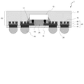
図1は、本発明による半導体装置の第1実施形態を示す断面図である。半導体装置1は、BGA型の半導体装置であり、半導体チップ10、樹脂層20、絶縁層30、および外部電極パッド40を備えている。樹脂層20は、封止樹脂22およびアンダーフィル樹脂24によって構成され、半導体チップ10を覆っている。なお、同図においては、半導体チップ10の全ての面が樹脂層20で覆われた例を示しているが、半導体チップ10の上面(電極端子12が設けられた面と反対側の面)は、樹脂層20で覆われていなくてもよい。すなわち、半導体チップ10の上面は、樹脂層20の表面に露出していてもよい。
FIG. 1 is a sectional view showing a first embodiment of a semiconductor device according to the present invention. The semiconductor device 1 is a BGA type semiconductor device, and includes a
樹脂層20上には、絶縁層30が形成されている。絶縁層30を構成する樹脂は、例えばポリイミド樹脂である。絶縁層30中には、外部電極パッド40が形成されている。この外部電極パッド40は、絶縁層30を貫通しており、その一面S1が絶縁層30の表面に露出するとともに、他面S2が樹脂層20の内部に位置している。外部電極パッド40の面S2には、凹部45が形成されている。この凹部45内には、樹脂層20を構成する樹脂(本実施形態においては封止樹脂22およびアンダーフィル樹脂24)が入り込んでいる。
An
具体的には、外部電極パッド40は、下層パッドメタル42(第1の導体パターン)および上層パッドメタル44(第2の導体パターン)によって構成されている。これらの下層パッドメタル42および上層パッドメタル44は、それぞれ絶縁層30および樹脂層20中に形成されている。図1からもわかるように、下層パッドメタル42は、側面の略全体が絶縁層30で覆われるとともに、上層パッドメタル44と反対側の面(外部電極パッド40の面S1に等しい)の略全体が絶縁層30の表面に露出している。また、上述の凹部45は、下層パッドメタル42および上層パッドメタル44のうち上層パッドメタル44に形成されている。凹部45の深さは、上層パッドメタル44の厚みに略等しい。
Specifically, the
上層パッドメタル44と同層中には、配線48が形成されている。この配線48は、上層パッドメタル44に接続されている。また、配線48の一部上には、電極バンプ50が形成されている。この電極バンプ50は、半導体チップ10の電極端子12に接続されている。電極端子12は、例えば半田バンプである。ただし、電極端子12は、Cu等の金属からなる基部上に半田膜が形成されたものであってもよい。その場合、当該半田膜が電極バンプ50に接続されることになる。さらに、外部電極パッド40の面S1上には、半導体装置1の外部電極端子として半田バンプ60が形成されている。
A
図2を参照しつつ、外部電極パッド40の構成をより詳細に説明する。同図は、半導体装置1の一部を示す断面図である。上述の下層パッドメタル42は、相異なる複数の金属膜によって構成された積層構造を有している。本実施形態において、この積層構造は、Cu膜42aと、当該Cu膜42aの上層パッドメタル44側の面上に形成されたNi膜42bとによって構成されている。
The configuration of the
同様に、上層パッドメタル44も、相異なる複数の金属膜によって構成された積層構造を有している。本実施形態において、この積層構造は、Cu膜44a(第1の金属膜)と、当該Cu膜44aの下層パッドメタル42と反対側の面上に形成されたNi膜44b(第2の金属膜)とによって構成されている。これらのCu膜44aおよびNi膜44bには、それぞれ開口45a(第1の開口)および開口45b(第2の開口)が形成されている。これらの開口45a,45bは、互いに連設されて凹部45を構成している。ここで、開口45aの開口面積は、開口45bのそれよりも大きい。換言すれば、Ni膜44bがCu膜44aに対してオーバーハングした構造となっている。それにより、凹部45の開口面(図2中に点線L1で示す)の面積は、凹部45の底面のそれよりも小さくなっている。
Similarly, the upper
また、配線48も、上層パッドメタル44と同様の積層構造、すなわちCu膜48aおよびNi膜48bによって構成された積層構造を有している。
The
図3を参照しつつ、凹部45の平面レイアウトの一例を説明する。同図は、図2のIII−III線に沿った平面図を示している。本実施形態においては、上層パッドメタル44(外部電極パッド40)1つあたりに複数(本例では4つ)の凹部45が設けられている。これら複数の凹部45は、平面視で、規則的に(本例では斜格子状に)配列されている。また、各凹部45は、矩形をしている。
An example of a planar layout of the
図4〜図8を参照しつつ、半導体装置1の製造方法の一例を説明する。まず、支持基板であるシリコンウエハ90上に、介在層としてCu膜92をスパッタ法等により形成する(図4(a))。次に、Cu膜92上に、ポリイミド樹脂等からなる絶縁層30を形成する。このとき、絶縁層30のうち、下層パッドメタル42が設けられる部分は開口しておく(図4(b))。なお、絶縁層30を構成する樹脂として感光性樹脂を用いることにより、このようにパターニングされた絶縁層30を低コストで形成することができる。
An example of a method for manufacturing the semiconductor device 1 will be described with reference to FIGS. First, a
続いて、Cu膜92をシード層としためっき法により、絶縁層30の上記開口に下層パッドメタル42を形成する(図5(a))。その後、セミアディティブ法により、上層パッドメタル44および配線48を形成する(図5(b))。具体的には、下層パッドメタル42が形成された絶縁層30上に、TiやCu等の金属膜をスパッタ法により形成した後、フォトレジストを塗布し、パターニングする。そして、めっき法により、そのフォトレジストの開口部内に上層パッドメタル44および配線48を形成する。その後、フォトレジストを除去し、スパッタ膜をエッチングする。このとき、上層パッドメタル44を構成するCu膜44a(図2参照)がサイドエッチされるようなエッチャントを選択することにより、Ni膜44bがCu膜44aに対してオーバーハングした構造を容易に実現することができる。
Subsequently, the lower
次に、配線48の一部上に、半導体チップ10の電極端子12と接続される電極バンプ50を形成する(図6(a))。続いて、電極バンプ50に、半導体チップ10の電極端子12を接続する。その後、半導体チップ10と絶縁層30との間の間隙にアンダーフィル樹脂24を注入することにより、両者間の接続部を樹脂封止する(図6(b))。このとき、アンダーフィル樹脂24は、上層パッドメタル44の凹部45内にも入り込むことになる。
Next, an
さらに、トランスファーモールド法、印刷法またはポッティング法等により、半導体チップ10を覆うように、絶縁層30上に封止樹脂22を形成する(図7(a))。このとき、封止樹脂22は、アンダーフィル樹脂24と同様に、凹部45内にも形成される。その後、シリコンウエハ90を除去する(図7(b))。続いて、Cu膜92もエッチングにより除去する(図8)。さらに、下層パッドメタル42上に半田バンプ60を接続することにより、図1の半導体装置1が得られる。
Further, a sealing
半導体装置1の効果を説明する。半導体装置1においては、外部電極パッド40の面S2に凹部45が設けられている。そして、その凹部45内に樹脂層20を構成する樹脂が入り込んでいる。これにより、外部電極パッド40と樹脂層20とが互いに噛み合った構造となるため、外部電極パッド40の上記面S2が平坦な場合に比して、外部電極パッド40と樹脂層20との界面で剥離が生じにくくなる。よって、外部電極パッド40と樹脂層20との間の接合信頼性に優れる半導体装置1が実現されている。この半導体装置1は、マザーボード等の実装基板に実装された際にも、その実装基板との間で高い接続信頼性を得ることができる。
The effect of the semiconductor device 1 will be described. In the semiconductor device 1, a
外部電極パッド40は、絶縁層30中に設けられた下層パッドメタル42と、樹脂層20中に設けられた上層パッドメタル44とを含んでおり、上層パッドメタル44に上記凹部45が設けられている。これにより、樹脂層20側の面に凹部45が設けられた外部電極パッド40を容易に製造することができる。
The
凹部45の深さは、上層パッドメタル44の厚みに略等しい。このような凹部45は、上層パッドメタル44のパターニングにより形成することができるため、製造が容易である。
The depth of the
上層パッドメタル44は、相異なる複数の金属膜によって構成された積層構造を有している。これにより、比較的上側の金属膜が比較的下側の金属膜に対してオーバーハングした構造を容易に実現することができる。実際、本実施形態において上層パッドメタル44は、図2で説明したとおり、Cu膜44aおよびNi膜44bの積層構造を有しており、Ni膜44bがCu膜44aに対してオーバーハングしている。かかる構造によれば、アンカー効果により、外部電極パッド40と樹脂層20との界面での剥離が一層生じにくくなる。
The upper
下層パッドメタル42は、Cu膜42aおよびNi膜42bの積層構造を有している。半田バンプ60に接続される側にCu膜42aが設けられているため、下層パッドメタル42と半田バンプ60との間で高い密着性を得ることができる。また、Ni膜42bは、バリアメタルとして機能させることができる。さらに、Cu膜42aと半田バンプ60を構成する半田との間に形成される合金により、Ni膜42bの析出を防ぐことができる。
The lower
下層パッドメタル42は、側面の略全体が絶縁層30で覆われるとともに、上層パッドメタル44と反対側の面(図1の面S1)の略全体が絶縁層30の表面に露出している。これにより、面S1の全体に半田バンプ60を接続することが可能となるため、半田バンプ60を微細なピッチで設けるのに適した構造が実現されている。
The lower
ところで、上記面S1の一部のみが露出し、残りの部分が絶縁層で覆われている場合には、その絶縁層によって外部電極パッド40が支えられた構成となる。これに対して、本実施形態のように面S1の全体が露出している場合には、かかる支えがないため、外部電極パッド40と樹脂層20との間での密着性が一層強く要求される。そのため、外部電極パッド40と樹脂層20との間の接合信頼性に優れる半導体装置1が一層有用となる。
By the way, when only a part of the surface S1 is exposed and the remaining part is covered with an insulating layer, the
複数の凹部45が1つの外部電極パッド40に設けられている。これにより、外部電極パッド40と樹脂層20との間の接合信頼性が一層向上する。また、複数の凹部45は、平面視で規則的に配列されているため、上層パッドメタル44のパターニングによって容易に形成することができる。
(第2実施形態)
A plurality of
(Second Embodiment)
図9は、本発明による半導体装置の第2実施形態を示す断面図である。半導体装置2は、BGA型の半導体装置であり、半導体チップ10、樹脂層20、絶縁層30、および外部電極パッド40を備えている。これらのうち半導体チップ10、樹脂層20および絶縁層30の構成は、半導体装置1について説明したものと同様である。半導体装置2においては、外部電極パッド40の構成が半導体装置1と相異する。
FIG. 9 is a sectional view showing a second embodiment of the semiconductor device according to the present invention. The
外部電極パッド40は、上述の下層パッドメタル42および上層パッドメタル44に加えて、それらの間に設けられた中間層パッドメタル46(第3の導体パターン)を有している。この中間層パッドメタル46は、樹脂層20中に形成されている。本実施形態において配線48は、中間層パッドメタル46と同層中に形成されている。それに伴い、電極バンプ50は、上層パッドメタル44と同層中に形成されている。
The
かかる構成の半導体装置2は、半導体装置1が奏する上述した効果に加えて、次の効果を奏する。すなわち、下層パッドメタル42と上層パッドメタル44との間に中間層パッドメタル46が介在することにより、外部電極パッド40全体の厚みが増大しているため、外部電極パッド40は機械的な応力を受けても変形しにくい。このことは、半導体装置2の信頼性の向上に寄与する。
In addition to the above-described effects that the semiconductor device 1 exhibits, the
本発明による半導体装置は、上記実施形態に限定されるものではなく、様々な変形が可能である。例えば、上記実施形態においては封止樹脂22およびアンダーフィル樹脂24の双方が凹部45内に入り込んだ構成を示したが、封止樹脂22およびアンダーフィル樹脂24のうち一方のみが凹部45内に入り込んだ構成としてもよい。
The semiconductor device according to the present invention is not limited to the above embodiment, and various modifications are possible. For example, in the above embodiment, the configuration in which both the sealing
また、凹部45の平面レイアウトとしては、図3に示したものに限らず、様々なものが考えられる。例えば、図10に示すように、円形の凹部45が斜格子状に配列されていてもよい。あるいは、図11に示すように、一方向に延在するトレンチ状の凹部45が、その延在方向と略垂直な方向に沿って配列されていてもよい。あるいは、図12および図13に示すように、凹部45は、上層パッドメタル44と共にモザイク模様を構成するように配列されていてもよい。この場合も、凹部45は斜格子状に配列されていると言うことができる。なお、図13は、図12において上層パッドメタル44および凹部45のパターンを反転させたものに相当する。
Further, the planar layout of the
1 半導体装置
2 半導体装置
10 半導体チップ
12 電極端子
20 樹脂層
22 封止樹脂
24 アンダーフィル樹脂
30 絶縁層
40 外部電極パッド
42 下層パッドメタル
44 上層パッドメタル
45 凹部
46 中間層パッドメタル
48 配線
50 電極バンプ
60 半田バンプ
DESCRIPTION OF SYMBOLS 1
Claims (10)
前記半導体チップを覆う樹脂層と、
前記樹脂層上に設けられた絶縁層と、
前記絶縁層を貫通するように設けられ、一面が前記絶縁層の表面に露出し、当該一面に外部電極端子が接続される外部電極パッドと、を備え、
前記外部電極パッドの他面には凹部が設けられており、当該凹部内に前記樹脂層を構成する樹脂が入り込んでおり、
前記外部電極パッドは、前記絶縁層中に設けられた第1の導体パターンと、前記樹脂層中に設けられた第2の導体パターンとを含んでおり、
前記第2の導体パターンに、前記凹部が設けられており、
前記第2の導体パターンは、相異なる複数の金属膜によって構成された積層構造を有しており、
前記積層構造は、第1の金属膜と、当該第1の金属膜の前記第1の導体パターンと反対側の面上に設けられた第2の金属膜とによって構成されており、
前記第1および第2の金属膜にはそれぞれ、互いに連設されて前記凹部を構成する第1および第2の開口が設けられており、
前記第1の開口は、前記第2の開口に比して開口面積が大きいことを特徴とする半導体装置。 A semiconductor chip;
A resin layer covering the semiconductor chip;
An insulating layer provided on the resin layer;
An external electrode pad provided so as to penetrate the insulating layer, one surface exposed on the surface of the insulating layer, and an external electrode terminal connected to the one surface;
A concave portion is provided on the other surface of the external electrode pad, and the resin constituting the resin layer enters the concave portion ,
The external electrode pad includes a first conductor pattern provided in the insulating layer and a second conductor pattern provided in the resin layer,
The recess is provided in the second conductor pattern,
The second conductor pattern has a laminated structure constituted by a plurality of different metal films,
The laminated structure includes a first metal film and a second metal film provided on a surface of the first metal film opposite to the first conductor pattern,
The first and second metal films are provided with first and second openings that are connected to each other to form the recess,
The semiconductor device according to claim 1, wherein the first opening has a larger opening area than the second opening .
前記第1および第2の導体パターンの間に設けられた第3の導体パターンを備える半導体装置。 The semiconductor device according to claim 1 ,
A semiconductor device comprising a third conductor pattern provided between the first and second conductor patterns.
前記凹部の深さは、前記第2の導体パターンの厚みに略等しい半導体装置。 The semiconductor device according to claim 1 or 2 ,
The depth of the recess is a semiconductor device substantially equal to the thickness of the second conductor pattern.
前記第1および第2の金属膜は、それぞれCu膜およびNi膜である半導体装置。 The semiconductor device according to claim 1 ,
The semiconductor device in which the first and second metal films are a Cu film and a Ni film, respectively.
前記第1の導体パターンは、相異なる複数の金属膜によって構成された積層構造を有している半導体装置。 The semiconductor device according to any one of claims 1 to 4,
The first conductor pattern is a semiconductor device having a laminated structure including a plurality of different metal films.
前記第1の導体パターンが有する前記積層構造は、Cu膜と、当該Cu膜の前記第2の導体パターン側の面上に設けられたNi膜とによって構成されている半導体装置。 The semiconductor device according to claim 5 ,
The stacked structure of the first conductor pattern is a semiconductor device including a Cu film and a Ni film provided on a surface of the Cu film on the second conductor pattern side.
前記第1の導体パターンは、側面の略全体が前記絶縁層で覆われるとともに、前記第2の導体パターンと反対側の面の略全体が前記絶縁層の表面に露出している半導体装置。 The semiconductor device according to any one of claims 1 to 6,
The first conductor pattern is a semiconductor device in which substantially the entire side surface of the first conductor pattern is covered with the insulating layer, and substantially the entire surface opposite to the second conductor pattern is exposed on the surface of the insulating layer.
前記凹部の開口面の面積は、当該凹部の底面の面積よりも小さい半導体装置。 The semiconductor device according to any one of claims 1 to 7,
The area of the opening surface of the recess is a semiconductor device smaller than the area of the bottom surface of the recess.
複数の前記凹部が1つの前記外部電極パッドに設けられている半導体装置。 The semiconductor device according to any one of claims 1 to 8,
A semiconductor device in which a plurality of the concave portions are provided in one external electrode pad.
前記複数の凹部は、平面視で規則的に配列されている半導体装置。 The semiconductor device according to claim 9 .
The semiconductor device in which the plurality of recesses are regularly arranged in a plan view.
Priority Applications (2)
| Application Number | Priority Date | Filing Date | Title |
|---|---|---|---|
| JP2005294940A JP5000877B2 (en) | 2005-10-07 | 2005-10-07 | Semiconductor device |
| US11/543,207 US7656046B2 (en) | 2005-07-10 | 2006-10-05 | Semiconductor device |
Applications Claiming Priority (1)
| Application Number | Priority Date | Filing Date | Title |
|---|---|---|---|
| JP2005294940A JP5000877B2 (en) | 2005-10-07 | 2005-10-07 | Semiconductor device |
Publications (2)
| Publication Number | Publication Date |
|---|---|
| JP2007103853A JP2007103853A (en) | 2007-04-19 |
| JP5000877B2 true JP5000877B2 (en) | 2012-08-15 |
Family
ID=38030462
Family Applications (1)
| Application Number | Title | Priority Date | Filing Date |
|---|---|---|---|
| JP2005294940A Active JP5000877B2 (en) | 2005-07-10 | 2005-10-07 | Semiconductor device |
Country Status (2)
| Country | Link |
|---|---|
| US (1) | US7656046B2 (en) |
| JP (1) | JP5000877B2 (en) |
Families Citing this family (6)
| Publication number | Priority date | Publication date | Assignee | Title |
|---|---|---|---|---|
| JP2008084959A (en) * | 2006-09-26 | 2008-04-10 | Shinko Electric Ind Co Ltd | Semiconductor device and manufacturing method thereof |
| US8373281B2 (en) * | 2008-07-31 | 2013-02-12 | Sanyo Electric Co., Ltd. | Semiconductor module and portable apparatus provided with semiconductor module |
| JP5261255B2 (en) | 2009-03-27 | 2013-08-14 | ルネサスエレクトロニクス株式会社 | Semiconductor device |
| CN106783633B (en) * | 2016-12-26 | 2020-02-14 | 通富微电子股份有限公司 | Fan-out packaging structure and packaging method thereof |
| IT201700055983A1 (en) * | 2017-05-23 | 2018-11-23 | St Microelectronics Srl | PROCEDURE FOR PRODUCING SEMICONDUCTOR, SEMICONDUCTOR AND CORRESPONDENT CIRCUIT DEVICES |
| JP2019054159A (en) * | 2017-09-15 | 2019-04-04 | 東芝メモリ株式会社 | Semiconductor device manufacturing method |
Family Cites Families (11)
| Publication number | Priority date | Publication date | Assignee | Title |
|---|---|---|---|---|
| US5355283A (en) * | 1993-04-14 | 1994-10-11 | Amkor Electronics, Inc. | Ball grid array with via interconnection |
| JP2595909B2 (en) * | 1994-09-14 | 1997-04-02 | 日本電気株式会社 | Semiconductor device |
| JP2001035886A (en) * | 1999-07-23 | 2001-02-09 | Nec Corp | Semiconductor device and its manufacture |
| JP3915337B2 (en) * | 1999-09-01 | 2007-05-16 | 松下電器産業株式会社 | Lead frame and method for manufacturing resin-encapsulated semiconductor device using the same |
| JP3812275B2 (en) * | 2000-03-24 | 2006-08-23 | 日立電線株式会社 | TAB tape and BGA structure |
| JP4068801B2 (en) * | 2000-11-30 | 2008-03-26 | 株式会社ルネサステクノロジ | Semiconductor device |
| JP4075306B2 (en) * | 2000-12-19 | 2008-04-16 | 日立電線株式会社 | Wiring board, LGA type semiconductor device, and method of manufacturing wiring board |
| JP3895570B2 (en) * | 2000-12-28 | 2007-03-22 | 株式会社ルネサステクノロジ | Semiconductor device |
| JP4663172B2 (en) * | 2001-07-31 | 2011-03-30 | 三洋電機株式会社 | Manufacturing method of semiconductor device |
| JP2003229514A (en) * | 2002-01-31 | 2003-08-15 | Hitachi Metals Ltd | Laminate and method of manufacturing resin sealing package |
| JP4108643B2 (en) * | 2004-05-12 | 2008-06-25 | 日本電気株式会社 | Wiring board and semiconductor package using the same |
-
2005
- 2005-10-07 JP JP2005294940A patent/JP5000877B2/en active Active
-
2006
- 2006-10-05 US US11/543,207 patent/US7656046B2/en active Active
Also Published As
| Publication number | Publication date |
|---|---|
| US20070158837A1 (en) | 2007-07-12 |
| US7656046B2 (en) | 2010-02-02 |
| JP2007103853A (en) | 2007-04-19 |
Similar Documents
| Publication | Publication Date | Title |
|---|---|---|
| JP3722209B2 (en) | Semiconductor device | |
| US9258899B2 (en) | Method of fabricating a wiring board | |
| US7129420B2 (en) | Semiconductor device and method for manufacture thereof, circuit board, and electronic instrument | |
| JP5143451B2 (en) | Semiconductor device and manufacturing method thereof | |
| KR100470386B1 (en) | Multi-chip Package | |
| US20070164457A1 (en) | Semiconductor package, substrate with conductive post, stacked type semiconductor device, manufacturing method of semiconductor package and manufacturing method of stacked type semiconductor device | |
| JP2017038075A (en) | Stackable molded ultra small electronic package including area array unit connector | |
| JP2008118140A (en) | Semiconductor chip stack package with reinforcing member for preventing warpage connected to substrate | |
| TW200832653A (en) | Package substrate, method of fabricating the same and chip package | |
| JP2002110898A (en) | Semiconductor device | |
| JP2009194079A (en) | WIRING BOARD FOR SEMICONDUCTOR DEVICE, MANUFACTURING METHOD THEREOF, AND SEMICONDUCTOR DEVICE USING THE SAME | |
| US7656046B2 (en) | Semiconductor device | |
| KR20240017393A (en) | Semiconductor device and manufacturing method thereof | |
| JP3402086B2 (en) | Semiconductor device and manufacturing method thereof | |
| CN100505224C (en) | Semiconductor device and semiconductor chip | |
| JP4498991B2 (en) | Semiconductor device and electronic device | |
| JP4494240B2 (en) | Resin-sealed semiconductor device | |
| JP4417974B2 (en) | Manufacturing method of stacked semiconductor device | |
| US6730539B2 (en) | Method of manufacturing semiconductor device package | |
| JP2012069804A (en) | Semiconductor device and manufacturing method therefor | |
| JP2020150172A (en) | Semiconductor device | |
| JP2004363224A (en) | Connection structure of semiconductor chip | |
| JP2004228142A (en) | Semiconductor device and multi-chip package | |
| JP2007335642A (en) | Package substrate | |
| TWI233671B (en) | Flip chip BGA |
Legal Events
| Date | Code | Title | Description |
|---|---|---|---|
| A621 | Written request for application examination |
Free format text: JAPANESE INTERMEDIATE CODE: A621 Effective date: 20080917 |
|
| A977 | Report on retrieval |
Free format text: JAPANESE INTERMEDIATE CODE: A971007 Effective date: 20101213 |
|
| A131 | Notification of reasons for refusal |
Free format text: JAPANESE INTERMEDIATE CODE: A131 Effective date: 20110215 |
|
| A131 | Notification of reasons for refusal |
Free format text: JAPANESE INTERMEDIATE CODE: A131 Effective date: 20120321 |
|
| A521 | Written amendment |
Free format text: JAPANESE INTERMEDIATE CODE: A523 Effective date: 20120425 |
|
| TRDD | Decision of grant or rejection written | ||
| A01 | Written decision to grant a patent or to grant a registration (utility model) |
Free format text: JAPANESE INTERMEDIATE CODE: A01 Effective date: 20120515 |
|
| A01 | Written decision to grant a patent or to grant a registration (utility model) |
Free format text: JAPANESE INTERMEDIATE CODE: A01 |
|
| A61 | First payment of annual fees (during grant procedure) |
Free format text: JAPANESE INTERMEDIATE CODE: A61 Effective date: 20120517 |
|
| R150 | Certificate of patent or registration of utility model |
Free format text: JAPANESE INTERMEDIATE CODE: R150 Ref document number: 5000877 Country of ref document: JP Free format text: JAPANESE INTERMEDIATE CODE: R150 |
|
| FPAY | Renewal fee payment (event date is renewal date of database) |
Free format text: PAYMENT UNTIL: 20150525 Year of fee payment: 3 |
|
| S531 | Written request for registration of change of domicile |
Free format text: JAPANESE INTERMEDIATE CODE: R313531 |
|
| R350 | Written notification of registration of transfer |
Free format text: JAPANESE INTERMEDIATE CODE: R350 |