JP4989900B2 - Parallel processing unit - Google Patents
Parallel processing unit Download PDFInfo
- Publication number
- JP4989900B2 JP4989900B2 JP2006023054A JP2006023054A JP4989900B2 JP 4989900 B2 JP4989900 B2 JP 4989900B2 JP 2006023054 A JP2006023054 A JP 2006023054A JP 2006023054 A JP2006023054 A JP 2006023054A JP 4989900 B2 JP4989900 B2 JP 4989900B2
- Authority
- JP
- Japan
- Prior art keywords
- data
- memory
- arithmetic processing
- bit
- circuit
- Prior art date
- Legal status (The legal status is an assumption and is not a legal conclusion. Google has not performed a legal analysis and makes no representation as to the accuracy of the status listed.)
- Expired - Fee Related
Links
Images


Classifications
-
- G—PHYSICS
- G06—COMPUTING OR CALCULATING; COUNTING
- G06F—ELECTRIC DIGITAL DATA PROCESSING
- G06F13/00—Interconnection of, or transfer of information or other signals between, memories, input/output devices or central processing units
- G06F13/14—Handling requests for interconnection or transfer
- G06F13/16—Handling requests for interconnection or transfer for access to memory bus
- G06F13/1605—Handling requests for interconnection or transfer for access to memory bus based on arbitration
- G06F13/1652—Handling requests for interconnection or transfer for access to memory bus based on arbitration in a multiprocessor architecture
-
- G—PHYSICS
- G11—INFORMATION STORAGE
- G11C—STATIC STORES
- G11C7/00—Arrangements for writing information into, or reading information out from, a digital store
- G11C7/10—Input/output [I/O] data interface arrangements, e.g. I/O data control circuits, I/O data buffers
- G11C7/1006—Data managing, e.g. manipulating data before writing or reading out, data bus switches or control circuits therefor
-
- Y—GENERAL TAGGING OF NEW TECHNOLOGICAL DEVELOPMENTS; GENERAL TAGGING OF CROSS-SECTIONAL TECHNOLOGIES SPANNING OVER SEVERAL SECTIONS OF THE IPC; TECHNICAL SUBJECTS COVERED BY FORMER USPC CROSS-REFERENCE ART COLLECTIONS [XRACs] AND DIGESTS
- Y02—TECHNOLOGIES OR APPLICATIONS FOR MITIGATION OR ADAPTATION AGAINST CLIMATE CHANGE
- Y02D—CLIMATE CHANGE MITIGATION TECHNOLOGIES IN INFORMATION AND COMMUNICATION TECHNOLOGIES [ICT], I.E. INFORMATION AND COMMUNICATION TECHNOLOGIES AIMING AT THE REDUCTION OF THEIR OWN ENERGY USE
- Y02D10/00—Energy efficient computing, e.g. low power processors, power management or thermal management
Landscapes
- Engineering & Computer Science (AREA)
- Theoretical Computer Science (AREA)
- Physics & Mathematics (AREA)
- General Engineering & Computer Science (AREA)
- General Physics & Mathematics (AREA)
- Static Random-Access Memory (AREA)
- Memory System (AREA)
- Dram (AREA)
Description
この発明は、並列演算処理装置に関し、特に、半導体メモリと演算器とが集積化された並列演算処理装置の構成に関する。 The present invention relates to a parallel arithmetic processing device, and more particularly to a configuration of a parallel arithmetic processing device in which a semiconductor memory and an arithmetic unit are integrated.
携帯機器分野および画像処理用途などにおいては、近年、その高性能化により、大量の音声または画像データを高速で処理することが要求されている。この大量のデータを処理する場合、一般に専用のDSP(デジタル・シグナル・プロセッサ)が用いられることが多い。しかしながら、この専用のDSPを用いた場合、そのハードウェアが固定的に設定され、データビット幅および処理内容が限定される。そこで、種々の用途に柔軟に対応するように、ソフトウェアにより機能を変更することができるプログラマブルプロセッサを用いて、これらの処理を実行することが要求されてきている。特に、このようなデータ処理システムは、小型化の観点から、小面積かつ低消費電力で高速処理を実現することが重要となってきている。 In recent years, in the field of portable equipment and image processing applications, it has been required to process a large amount of sound or image data at high speed due to its high performance. When processing a large amount of data, a dedicated DSP (digital signal processor) is often used in general. However, when this dedicated DSP is used, its hardware is fixedly set, and the data bit width and processing contents are limited. Therefore, it has been required to execute these processes by using a programmable processor whose function can be changed by software so as to flexibly cope with various applications. In particular, it is important for such a data processing system to realize high-speed processing with a small area and low power consumption from the viewpoint of miniaturization.
音声データおよび画像データなどの処理においては、複数組のデータに対し、同じ演算処理を実行することが多い。したがって、このような処理用途において、SIMD型(シングル・イントラクション・ストリーム・マルチプル・データ・ストリーム:Single Instruction Stream Multiple Data Stream)プロセッサが用いられることが多い。このSIMD型プロセッサにおいては、各々がレジスタファイルと演算器とで構成されるプロセッサエレメントを並列に設け、各プロセッサエレメントを同一命令で並列に動作させる。このプロセッサエレメントは、たとえば、特許文献1(特開2003−186854号公報)に示されるように、256個が並列に設けられ、256組のデータについて並列演算処理を行なうことができる。
SIMD型プロセッサにおいては、各プロセッサエレメントにおいて多ビットデータをレジスタファイルに格納する。レジスタからの多ビットデータを対応の演算器で受けて演算処理を実行する。この演算結果は、対応のレジスタファイルのレジスタに格納される。したがって、演算データのビット幅は、演算器またはレジスタのビット幅で決定される。上述の特許文献1に示されるように、レジスタファイルにおいて演算に利用するレジスタの数を変更することにより、演算データのビット幅の変更に対応することが可能である。しかしながら、たとえば8ビットレジスタを用いて16ビット演算データを格納する場合、上位ビットレジスタおよび下位ビットレジスタを設定し、順次レジスタを切換えて演算処理を行なう必要がある。したがって、たとえば、ブースアルゴリズムに従って乗算処理を行なう場合、部分積を求め、次いで部分析を加算して最終積を求める操作を実行する際に、演算データの桁位置を合わせるためにレジスタの切換が極めて煩雑となるという問題が生じる。
In the SIMD type processor, multi-bit data is stored in a register file in each processor element. Multi-bit data from the register is received by a corresponding arithmetic unit to execute arithmetic processing. The calculation result is stored in the register of the corresponding register file. Therefore, the bit width of the operation data is determined by the bit width of the operation unit or the register. As described in
また、レジスタの切換の有無に応じて処理手順を変更する必要がある。従って、演算データのビット幅に応じて処理手順を変更する必要が生じ、ビット幅変更に対して柔軟に対応することができなくなる。 Further, it is necessary to change the processing procedure depending on whether or not the register is switched. Therefore, it is necessary to change the processing procedure according to the bit width of the operation data, and it becomes impossible to flexibly cope with the bit width change.
また、SIMD型プロセッサにおいては、多ビットデータの並列演算処理が行なわれており、演算器は、多ビット演算器であり、その占有面積が大きくなり、小型化に対する障害となる。 Further, in the SIMD type processor, multi-bit data is processed in parallel, and the arithmetic unit is a multi-bit arithmetic unit, which occupies a large area and becomes an obstacle to miniaturization.
上述のようなSIMD型プロセッサの問題を解消するために、本願発明者のグループは、先に、高速演算処理を実現する並列演算処理装置を提案している(たとえば特願2004−171658号)。この並列演算処理装置においては、基本構成として、メモリセルアレイを複数のエントリに分割し、エントリに対応して、1ビット演算器を配置する。各エントリに、演算データを格納する。各演算器において、ビットシリアルに、演算処理を実行する。たとえば、演算器の両側のメモリセルアレイのエントリ各々からデータビットを読出して、対応の演算器へ転送し、演算器において演算を実行し、その実行結果を、所定のエントリに格納する。 In order to solve the problems of the SIMD type processor as described above, the group of the inventors of the present application has previously proposed a parallel arithmetic processing device that realizes high-speed arithmetic processing (for example, Japanese Patent Application No. 2004-171658). In this parallel arithmetic processing unit, as a basic configuration, the memory cell array is divided into a plurality of entries, and a 1-bit arithmetic unit is arranged corresponding to the entries. Calculation data is stored in each entry. In each arithmetic unit, arithmetic processing is executed in bit serial. For example, the data bits are read from each of the memory cell array entries on both sides of the arithmetic unit, transferred to the corresponding arithmetic unit, the arithmetic unit executes the operation, and the execution result is stored in a predetermined entry.
演算処理は、複数ワードについてビットシリアルに行なわれる(ワードパラレル・ビットシリアル)。したがって、個々のデータの演算には時間を要するものの、エントリ数を多くして演算の並列度を高くすることにより、高速処理が実現される。たとえば、データビットの読出、書込および演算各々に1マシンサイクルが必要とされる動作環境においては、1ビット演算処理に3マシンサイクルが必要となる。したがって、8ビットデータの処理には3・8=24マシンサイクルが必要となる。しかしながら、エントリ数がたとえば1024であれば、24マシンサイクルで1024組のデータ処理が完了する。演算データのビット幅は、32ビットまたは64ビットである。従って、エントリの数を増大させることにより、高速演算が実現される。 Arithmetic processing is performed in bit serial for a plurality of words (word parallel / bit serial). Therefore, although calculation of individual data requires time, high-speed processing is realized by increasing the number of entries and increasing the parallelism of the calculation. For example, in an operating environment that requires one machine cycle for each reading, writing, and operation of data bits, three machine cycles are required for 1-bit operation processing. Therefore, processing of 8-bit data requires 3 · 8 = 24 machine cycles. However, if the number of entries is 1024, for example, 1024 sets of data processing are completed in 24 machine cycles. The bit width of the operation data is 32 bits or 64 bits. Therefore, high-speed computation is realized by increasing the number of entries.
また、演算処理が、ビットシリアル態様で行なわれるため、演算データのビット幅の変更に対しては、エントリのアクセスするアドレス範囲を変更することにより対応することができる。レジスタ切換などの処理手順の変更は不要であり、演算データのビット幅の変更に対して容易に対応することができる。 Since the arithmetic processing is performed in a bit serial manner, the change of the bit width of the arithmetic data can be dealt with by changing the address range accessed by the entry. It is not necessary to change the processing procedure such as register switching, and it is possible to easily cope with a change in the bit width of the operation data.
また、演算器は1ビット演算器であり、そのレイアウト面積は小さくすることができる。また、メモリセルアレイのビット線をエントリとして利用する場合、エントリに対応して演算器を配置することができ、レイアウト面積が小さく演算の並列度の極めて高い並列演算処理装置を実現することができる。 The computing unit is a 1-bit computing unit, and its layout area can be reduced. Further, when the bit line of the memory cell array is used as an entry, an arithmetic unit can be arranged corresponding to the entry, and a parallel arithmetic processing device having a small layout area and an extremely high parallel degree of arithmetic can be realized.
より演算の並列度を上げるためには、より効率的に演算器およびメモリセルアレイの周辺回路を配置する必要がある。しかしながら、この演算器および周辺回路の配置領域は、メモリセルのピッチに従って決定される。メモリセルアレイにおけるレイアウトルールおよびメモリセルのピッチが予め設定されているため、より効率的にレイアウト面積を低減して演算器および周辺回路を配置するためには、さらなる工夫を必要とする。 In order to further increase the degree of parallelism of operations, it is necessary to more efficiently arrange the arithmetic units and peripheral circuits of the memory cell array. However, the arrangement area of the arithmetic unit and the peripheral circuit is determined according to the pitch of the memory cells. Since the layout rule and the pitch of the memory cells in the memory cell array are set in advance, further contrivance is required in order to more efficiently reduce the layout area and arrange the arithmetic units and peripheral circuits.
また、メモリセルアレイは、リフレッシュが不要なたとえばSRAM(スタティック・ランダム・アクセス・メモリ)で構成される。データがビットシリアルに演算処理されるため、高速処理のために、データの読出と演算結果の書込を同一サイクルで行うリードモディファイを行う場合、データの読出および書込を1マシンサイクルで行なうSRAMの方が、演算器よりも動作周波数が高くなる。この結果、このSRAMの動作周波数により並列演算処理装置全体の動作速度が律速され、より高速演算処理を実現するためには、また、SRAMの動作方式に対してさらに工夫が必要となる。 The memory cell array is composed of, for example, an SRAM (Static Random Access Memory) that does not require refreshing. Since data is arithmetically processed in bit serial, for high-speed processing, when performing read modification in which data is read and arithmetic results are written in the same cycle, an SRAM in which data is read and written in one machine cycle The operating frequency is higher than that of the computing unit. As a result, the operating speed of the entire parallel arithmetic processing unit is limited by the operating frequency of the SRAM, and in order to realize higher speed arithmetic processing, further improvements to the SRAM operating method are required.
また、動作周波数を高くした場合、消費電力が増大する。また、高速化のためには、素子のレイアウト面積を大きくして、電流駆動力を高くする必要があり、消費電力が増大する。さらに、演算の並列度を高くするためには、エントリの数を増大させる必要があり、この場合、並行して動作する回路の数が増大し、消費電力が増大する。したがって、演算の並列度および動作速度を消費電力を増大させることなく高くするためには、この点からもさらなる工夫が必要となる。 Also, when the operating frequency is increased, power consumption increases. Further, in order to increase the speed, it is necessary to increase the layout area of the element and increase the current driving capability, which increases power consumption. Furthermore, in order to increase the degree of parallelism of operations, it is necessary to increase the number of entries. In this case, the number of circuits operating in parallel increases and power consumption increases. Therefore, in order to increase the parallelism and the operation speed of the operation without increasing the power consumption, further ingenuity is required from this point.
それゆえ、この発明の目的は、低消費電力で高速動作および超高並列演算を実現することのできる並列演算処理装置を提供することである。 SUMMARY OF THE INVENTION Therefore, an object of the present invention is to provide a parallel arithmetic processing device capable of realizing high-speed operation and ultra-high parallel arithmetic with low power consumption.
この発明に係る並列演算処理装置は、行列状に配列される複数のメモリセルと、メモリセル各列に対応して配置される複数のビット線とを各々が有する複数のメモリブロックと、これらの複数のメモリブロックの間に配置され、各々が、それぞれ与えられたデータに対して演算処理を実行する複数の演算器を有する複数の演算処理ユニットと、メモリブロック各々においてビット線の両側に交互に配置され、隣接する演算処理ユニットの演算器との間でデータを転送する複数のデータ書込/読出回路を含むデータ転送回路とを備える。複数のメモリブロックは、各々が、一方向に整列するメモリブロックを含む複数のメモリマットに分割され、データ転送回路および演算処理ユニットの動作を制御するローカル制御回路は、メモリマットの間の領域に配置される。 The parallel processing device according to the present invention includes a plurality of memory blocks each having a plurality of memory cells arranged in a matrix and a plurality of bit lines arranged corresponding to each column of the memory cells, and Arranged between a plurality of memory blocks, each of which has a plurality of arithmetic processing units each having a plurality of arithmetic units for performing arithmetic processing on given data, and alternately on both sides of the bit line in each memory block And a data transfer circuit including a plurality of data write / read circuits for transferring data to and from an arithmetic unit of an adjacent arithmetic processing unit. The plurality of memory blocks are each divided into a plurality of memory mats including memory blocks aligned in one direction, and the local control circuit that controls the operation of the data transfer circuit and the arithmetic processing unit is provided in an area between the memory mats. Be placed.
各メモリブロックにおいてビット線の両側にデータ転送回路のデータ書込/読出回路が交互に配置される。これにより、データ転送回路および演算処理ユニットの演算器のピッチ条件が緩和され、効率的に余裕を持ってこれらの回路要素を配置することができる。また、1つのデータ転送回路において配置されるデータ書込/読出回路の数が低減され、入出力データ1ビットあたりの列(ビット線)の数が低減され、レイアウト面積が低減され、また、動作する回路の数も低減され消費電力が低減される。 In each memory block, data write / read circuits of the data transfer circuit are alternately arranged on both sides of the bit line. As a result, the pitch conditions of the data transfer circuit and the arithmetic unit of the arithmetic processing unit are relaxed, and these circuit elements can be arranged efficiently with a margin. Also, the number of data write / read circuits arranged in one data transfer circuit is reduced, the number of columns (bit lines) per bit of input / output data is reduced, the layout area is reduced, and the operation The number of circuits to be reduced is also reduced, and power consumption is reduced.
また、メモリブロックの間には、演算処理ユニットが配置されるため、メモリブロック間の、ダミーセル等を配置する分離領域が不要となり、メモリセルアレイの面積を低減することができる。 In addition, since an arithmetic processing unit is arranged between the memory blocks, an isolation region for arranging dummy cells or the like between the memory blocks becomes unnecessary, and the area of the memory cell array can be reduced.
さらに、メモリブロックにおいて、1本のワード線を選択することにより、メモリブロック両側の演算回路へ転送するデータを並行して選択することができる。したがって、各メモリブロックをバンクとして利用して並列演算を行なう場合、2つのバンクの演算データを1つのワード線の選択で読出/書込を行なうことができ、選択ワード線の本数を低減でき、応じてワード線選択に要する消費電力を低減することができる。 Further, by selecting one word line in the memory block, data to be transferred to the arithmetic circuits on both sides of the memory block can be selected in parallel. Therefore, when performing parallel operations using each memory block as a bank, the operation data of two banks can be read / written by selecting one word line, and the number of selected word lines can be reduced. Accordingly, power consumption required for word line selection can be reduced.
[出発構成]
図1は、この発明に従う並列演算処理装置を利用するシステムの概念的構成を示す図である。この発明に従う並列演算処理装置は、図1に示す演算装置をチップ上に実現する。先ず、この発明に従う並列演算処理装置の動作および機能を明確にするために、図1を参照して、並列演算処理装置を利用する処理システムの概念的構成および演算操作について説明する。
[Departure composition]
FIG. 1 is a diagram showing a conceptual configuration of a system using a parallel arithmetic processing device according to the present invention. The parallel arithmetic processing device according to the present invention implements the arithmetic device shown in FIG. 1 on a chip. First, in order to clarify the operation and function of the parallel arithmetic processing device according to the present invention, the conceptual configuration and arithmetic operation of a processing system using the parallel arithmetic processing device will be described with reference to FIG.
図1において、演算処理システムは、並列演算を実行する半導体演算装置1と、この半導体演算装置1における処理の制御、システム全体の制御およびデータ処理を行なうホストCPU2と、システムの主記憶として利用されて必要な種々のデータを格納するメモリ3と、ホストCPU2を介することなくメモリ3に直接アクセスするDMA(ダイレクト・メモリ・アクセス)回路4とを含む。DMA回路4の制御により、メモリ3と半導体演算装置1の間でデータ転送を行なうことができ、また半導体演算装置1へ直接アクセスすることができる。
In FIG. 1, an arithmetic processing system is used as a
ホストCPU2、メモリ3、DMA回路4、および半導体演算装置1は、システムバス5を介して相互接続される。半導体演算装置1は、複数の並列に設けられる基本演算ブロックFB1−FBnと、システムバス5との間でデータ/命令を転送する入出力回路10と、半導体演算装置1内部での動作処理を制御する集中制御回路15を含む。
The
基本演算ブロックFB1−FBnは、内部データバス(グローバルデータバス)12に結合され、また集中制御ユニット15、入出力回路10および基本演算ブロックFB1−FBnは、内部バス14に結合される。基本演算ブロックFB(FB1−FBnを総称的に示す)の間には、ブロック間データバス16が設けられる(図1において、基本演算ブロックFB1およびFB2の間に配置される隣接ブロック間データバス16を代表的に示す)。
Basic operation blocks FB 1 -FBn are coupled to internal data bus (global data bus) 12, and
基本演算ブロックFB1−FBnを並列に設け、この半導体演算装置1の内部で並列に同一または異なる演算処理を実行する。これらの基本演算ブロックFB1−FBnは、同一構成を有するため、図1においては基本演算ブロックFB1の構成を代表的に示す。
Basic arithmetic blocks FB1-FBn are provided in parallel, and the same or different arithmetic processing is executed in parallel inside the
基本演算ブロックFB1は、メモリセルが行列状に配列されるメモリマットおよび演算器を含む主演算回路20と、マイクロコード化された実行プログラムを格納するマイクロプログラム格納メモリ23と、基本演算ブロックFB1の内部動作を制御するコントローラ21と、アドレスポインタ等として用いられるレジスタ群22と、主演算回路20における不良の救済を行なうためのヒューズプログラムを実行するためのヒューズ回路24を含む。
The basic arithmetic block FB1 includes a main
コントローラ21は、ホストCPU2からシステムバス5および入出力回路10を介して与えられる制御命令により制御が手渡され、対応の基本演算ブロックFB1−FBnの動作を制御する。これらの基本演算ブロックFB1−FBnにマイクロプログラム命令メモリ23を設け、コントローラ21がこのメモリ23内に実行プログラムを格納することにより、基本演算ブロックFB1−FBnそれぞれにおいて実行する処理内容を変更することができ、基本演算ブロックFB1−FBnにおいてそれぞれ演算実行される処理内容を変更することができる。
The
隣接ブロック間データバス16が、基本演算ブロックFB1−FBnの間のデータ転送を行なうために設けられる。この隣接ブロック間データバス16は、内部データバス(グローバルデータバス)を占有することなく基本演算ブロック間の高速データ転送を可能とする。したがって、たとえば、ある基本演算ブロックに内部データバス12を介してデータを転送している間に、別の基本演算ブロック間でデータ転送を行なうことができる。
A
集中制御ユニット15は、制御用CPU25と、この制御用CPUが実行する命令を格納する命令メモリ26と、制御用CPU25のワーキングレジスタまたはポインタ格納用のレジスタを含むレジスタ群27と、マイクロプログラムのライブラリを格納するマイクロプログラムライブラリ格納メモリ28を含む。集中制御ユニット15は、内部バス14を介してホストCPU2から制御権を手渡され、内部バス14を介して基本演算ブロックFB1−FBnの処理動作を制御する。
The
このマイクロプログラムライブラリ格納メモリ28に、各種シーケンス処理がコード化されたマイクロプログラムをライブラリとして格納することにより、集中制御ユニット15から必要なマイクロプログラムを選択して、基本演算ブロックFB1−FBnのマイクロプログラム格納メモリ23に格納されるマイクロプログラムを変更することができ、処理内容の変更に柔軟に対応することができる。
In the microprogram
ヒューズ回路24は、この基本演算ブロックFB1−FBnそれぞれにおいて、不良が発生した場合冗長置換を用いて不良救済を行ない、これにより、歩留まりを改善する。 In each of the basic operation blocks FB1 to FBn, the fuse circuit 24 performs defect repair using redundant replacement when a defect occurs, thereby improving the yield.
図2は、図1に示す主演算回路20の基本的な構成を概略的に示す図である。図2において、主演算回路20は、メモリセルマット30Aおよび30Bと、これらのメモリセルマット30Aおよび30Bの間に配置される演算処理ユニット32を備える。
FIG. 2 schematically shows a basic configuration of main
メモリセルマット30Aおよび30Bは、基本的にそれぞれm個のエントリERYに分割される。エントリERYは、nビットのビット幅を有する。このメモリセルマットの詳細構成については後に説明する。メモリセルマット30Aおよび30Bにおいて、各エントリERYを構成するメモリセルMCは、スタティック・ランダム・アクセス・メモリセルで構成される。
この演算処理ユニット32は、メモリセルマット30Aおよび30BのエントリERYに対応して設けられる演算器(ALU)34を含む。図2においては、演算器(以下、単にALUと称す)34は、1ビット演算処理を実行するように示される。しかしながら、このALUは、2ビット演算処理を実行してもよい。この演算処理ユニット32においてALU34が、それぞれ対応のエントリのデータに対して指定された演算処理を行なう。このALU34は、加算、減算、論理積、排他的論理和などの演算を実行することができる。
二項演算をALU34が行なう場合、メモリセルマット30Aおよび30Bに、各項の演算対象データを格納し、その演算処理結果を、メモリセルマット30Aおよび30Bの一方に格納する。ALU34に対しエントリERYの演算対象データのビットが逐次読出され、ビットシリアルに演算が実行される。図2においては、メモリセルマット30Aおよび30Bそれぞれに対し、メモリセルMCのデータを読出してALU34へ転送し(ロードし)、その演算結果がメモリセルに格納される(ストアされる)ように示す。
When the
メモリセルマット30Aおよび30Bは、各々演算対象の組のデータをともに格納することは要求されず、1つのメモリセルマットに格納するデータ量を低減することができる。応じて、ビット線(エントリERYがビット線延在方向に沿って形成される)の長さを短くすることができ、高速データ転送を実現する。
図3は、図1に示す隣接ブロック間データバス16の具体的接続態様を、主演算回路の具体的配置とともに併せて示す図である。図3において、主演算回路20A−20Dが図1に示す内部データバス12に対応するグローバルデータバスGBSに並列に結合される。これらの主演算回路20A−20Dの各々は、メモリセルマット30Aおよび30Bと、これらのメモリセルマット30Aおよび30Bの間に配設されるALU群(演算処理ユニット)を含む。図3においては、このALU群は示していない。各主演算回路においてALU群のALU(34)を相互接続するためのALU間相互接続用スイッチ回路ECMが設けられる。このALU間相互接続用スイッチ回路ECMにより、物理的に離れた位置のエントリのデータに対して演算処理を実行することができる。
FIG. 3 is a diagram showing a specific connection mode of the
メモリセルマット30Aおよび30Bは、各々、複数のエントリERYに分割されており、ALU間相互接続用スイッチ回路ECM内において、エントリERYそれぞれに対して、ALU間相互接続回路が設けられる。
図1に示す隣接ブロック間データバス16は、隣接する主演算回路のALU間接続回路(ALU間相互接続用スイッチ回路ECM内)を相互接続する隣接ブロックエントリ相互接続線40を含む。隣接ブロックエントリ相互接続線40は、隣接する基本演算ブロックの主演算回路20(20A−20D)の同一位置のエントリを相互接続する。
The inter-adjacent
グローバルデータバスGBSは、入出力回路10を介して外部のシステムバス5に結合される。図3においては、外部システムバス5が一例として32ビット幅の場合を示す。グローバルデータバスGBSに関して同一側に配置される隣接主演算回路20Aおよび20Bは、同一位置のエントリのALUが、隣接ブロックエントリ相互接続バスNBAaを介して相互接続される。この隣接ブロックエントリ相互接続バスNBAaは、隣接する主演算回路20Aおよび20Bの同一位置のエントリERYに対して設けられALUおよびALU間接続回路を相互接続する隣接ブロックエントリ接続線40を含む。
Global data bus GBS is coupled to
また、グローバルデータバスGBSの他方側において配置される隣接主演算回路20Cおよび20Dにおいても、隣接ブロックエントリ接続バスNBAbが配置される。この隣接ブロックエントリ相互接続バスNBAbは、主演算回路20Cおよび20Dの同一位置にエントリERYに対して設けられるALUおよびALU間相互接続回路を接続する隣接ブロックエントリ相互接続線40を含む。
In adjacent main arithmetic circuits 20C and 20D arranged on the other side of global data bus GBS, adjacent block entry connection bus NBAb is also arranged. This adjacent block entry interconnection bus NBAb includes an adjacent block
隣接ブロック間相互接続バス(隣接ブロック間データバス16)は、さらに、グローバルデータバスBGSに対して対向する位置の主演算回路20Aおよび20Cの対応するエントリERYに対して設けられるALUおよびALU間相互接続回路を接続する隣接ブロックエントリ相互接続バスNBBaを含む。この隣接ブロックエントリ相互接続バスNBBaは、主演算回路20Aおよび20Cの対応の位置のエントリに対して設けられるALUユニットおよびALU間接続回路相互接続する配線42aを含む。
The inter-adjacent block interconnection bus (adjacent block data bus 16) is further connected between the ALU and ALU provided for the corresponding entry ERY of the main
同様に、主演算回路20Bおよび20Dの対応の位置のエントリERYに対して配置されるALUおよびALU間接続回路が、隣接ブロック相互接続バスNBBbより相互接続される。この隣接ブロックエントリ相互接続バスNBBbは、各ALUおよびALU間接続回路に対して配設される配線42bを含む。
Similarly, the ALU and inter-ALU connection circuit arranged for the entry ERY at the corresponding position of the main
この図3に示すように、基本演算ブロックFBi(主演算回路20A−20D)が配設され、グローバルデータバスGBSの一方側の両端の主演算回路およびグローバルデータバスの他方側の主演算回路のALUおよびALU間接続回路を相互接続することにより、これらの主演算回路20A−20Dをリング状に相互接続することができ、任意の主演算回路間でデータ転送を行なうことができる。また、アレイ状に主演算回路のメモリセルマットを配置することにより、効率的にメモリセルマットを配置することができる。
As shown in FIG. 3, basic operation blocks FBi (
図3に示すように、隣接ブロック相互接続バスNBBaおよびNBBbにおいて、対向して配置される主演算回路の同一位置のエントリERYに対して設けられるALUおよびALU間相互接続回路が、配線42aおよび42bにより相互接続されている。したがって、その相互接続配線42aおよび42bは、それぞれのバスNBBaおよびNBBbにおいて同じ長さとなり、信号伝搬遅延を同一とすることができ、信号のスキューを低減でき、高速転送を実現することができる。
As shown in FIG. 3, in the adjacent block interconnection buses NBBa and NBBb, the ALU and ALU interconnection circuit provided for the entry ERY at the same position of the main arithmetic circuit arranged facing each other is connected to the
また、隣接ブロックエントリ相互接続バスNBBaおよびNBBbは、それぞれメモリセルマット30Aおよび30B上に延在される第1の配線部分と、グローバルデータバスBGSに関して対向する主演算かリロードのメモリセルマット上を第1の配線部分と直交する方向に延在する第2の配線部分とで構成される。これらの第1の配線部分および第2の配線部分をメモリセルマット上で相互接続することにより、グローバルデータバスに対して対向するメモリマット間の相互接続配線をコンパクトに配置することができ、配線面積増大によるアレイ面積の増大を抑制することができる。
Adjacent block entry interconnection buses NBBa and NBBb are connected to the first wiring portion extending on
なお、図3において、ALU間相互接続用スイッチ回路ECMの内部構成は示していない。ALU間相互接続用スイッチ回路ECMにおいては、ALUおよびALU間接続回路がエントリに対応して配置されており、各ALUおよびALU間接続回路が、対応の配線40、42aまたは42bにより接続される。
In FIG. 3, the internal configuration of the inter-ALU interconnection switch circuit ECM is not shown. In the inter-ALU interconnection switch circuit ECM, the ALU and the inter-ALU connection circuit are arranged corresponding to the entries, and each ALU and the inter-ALU connection circuit are connected by the corresponding
本発明は、これらの図1から図3に示す構成を基本構成として、半導体チップ上に主演算回路(基本演算ブロック)を効率的に集積化して、低消費電力で高速で動作する並列演算処理装置を実現する。 The present invention is based on the configuration shown in FIGS. 1 to 3 as a basic configuration, and a parallel arithmetic processing that operates at high speed with low power consumption by efficiently integrating a main arithmetic circuit (basic arithmetic block) on a semiconductor chip. Realize the device.
[実施の形態1]
図4は、この発明の実施の形態1に従う並列演算処理装置の全体の構成を概略的に示す図である。図4において、並列演算処理装置50は、半導体チップ上に集積化され、2つのメモリマット55Aおよび55Bを含む。この図4に示す並列演算処理装置50は、1つの基本演算ブロックを構成してもよく、また図3に示すように、複数の主演算回路を含んでもよい。
[Embodiment 1]
FIG. 4 schematically shows an overall configuration of the parallel arithmetic processing device according to the first embodiment of the present invention. In FIG. 4, a
また、この並列演算処理装置50は、半導体チップ単体で構成されてもよく(領域50がチップに対応)、また、他の装置と同一チップ上に集積化されてシステムLSIを構成しても良い(領域50が、いわゆるマクロに対応)。
Further, the
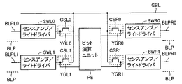
メモリマット55Aは、メモリブロックMA0−MAmを含み、メモリマット55Bは、メモリブロックMB0−MBmを含む。メモリマット55Aにおいて、メモリブロックの間に、演算処理ユニットPA0−PAm−1が配設される。これらの演算処理ユニットPA0−PAm−1は、両側に設けられるデータ転送回路を構成するセンスアンプ/ライトドライバT帯XA0−TXAk−1を介して隣接メモリブロックと結合される。メモリマット55Bにおいても、同様、メモリブロックMB0−MBmの間に、演算処理ユニットPB0−PBm−1が配設される。演算処理ユニットPB0−PAm−1と各メモリブロックとの間には、センスアンプ/ライトドライバTXB0−TXBk−1帯がそれぞれ配置される。センスアンプ/ライトドライバ帯TXA0−TXAk−1およびTXB0−TXBk−1は、各々、センスアンプおよびライトドライバを含む。
これらのメモリマット55Aおよび55Bの間の領域に、メモリブロックMA0−MAmおよびMB0−MBmに対応してSRAM周辺回路SH0−SHmが配置される。また、メモリマット55Aおよび55Bの演算処理ユニットPA0−PAm−1およびPB0−PBm−1の間の領域にローカル制御回路LK0−LKm−1が配置される。
SRAM peripheral circuits SH0-SHm are arranged corresponding to memory blocks MA0-MAm and MB0-MBm in an area between
メモリブロックMA0−MAmおよびMB0−MBmは、各々SRAMセルで構成され、メモリブロックにおけるメモリセルのデータの書込および読出を行なうためのロウデコーダ、ワード線ドライブ回路およびワード線選択タイミングの制御を行う制御回路などの周辺回路が、SRAM周辺回路内SH0−SHmに配置される。 Memory blocks MA0-MAm and MB0-MBm are each composed of SRAM cells, and control row decoders, word line drive circuits, and word line selection timings for writing and reading data of memory cells in the memory blocks. Peripheral circuits such as a control circuit are arranged in the SRAM peripheral circuits SH0 to SHm.
ローカル周辺回路LK0−LKm−1は、対応の演算処理ユニットにおける演算処理動作を制御するとともに、対応のセンスアンプ/ライトドライバ帯のセンスアンプおよびライトドライバの動作を制御する。 Local peripheral circuits LK0-LKm-1 control the arithmetic processing operation in the corresponding arithmetic processing unit, and also control the operations of the sense amplifier and write driver in the corresponding sense amplifier / write driver band.
メモリマット55Aおよび55Bの間に、SRAM周辺回路SH0−SHmおよびローカル制御回路LK0−LKm−1を配置することにより、蝋アドレスを精製するアドレスポインタおよびロウアドレスデコード回路などの周辺回路を、メモリマット55Aおよび55Bで共有することができる。これにより、SRAM周辺回路のレイアウト面積を低減することができる。
By arranging SRAM peripheral circuits SH0-SHm and local control circuits LK0-LKm-1 between
また、ローカル制御回路LK0−LKm−1においても、マット特定信号を除いて、内部制御信号を生成する回路部分を、メモリマット間で共有することができる。また、これらの演算処理ユニットが、並列に同一の演算を実行する場合には、ローカル制御回路において演算制御を行う回路部分をメモリマット55Aおよび55B間で共有することができ、応じて、レイアウト面積を低減することができる。
Also in the local control circuits LK0 to LKm-1, a circuit portion for generating an internal control signal can be shared between the memory mats except for the mat specific signal. In addition, when these arithmetic processing units execute the same operation in parallel, a circuit portion that performs arithmetic control in the local control circuit can be shared between the
メモリブロックの内部構成については、後に詳細に説明するが、1つのメモリブロックMAiおよびMBi(i=0−m)は、各々、その両側の演算処理ユニットにより用いられる。すなわち、図3に示すように、演算処理回路(回路ECMで表わす回路部分)が、その両側のメモリセルマットで共有されるのではなく、図4に示す構成においては、演算処理ユニットがメモリブロックを共有する。したがって、図3に示すように、主演算回路の間のメモリセルマット間の領域において、演算処理ユニットが配置される構成となり、ダミーセルなどの回路領域等のSRAMブロックを分離する領域が不要となり、レイアウト面積を低減することができる。 Although the internal configuration of the memory block will be described in detail later, each of the memory blocks MAi and MBi (i = 0-m) is used by the arithmetic processing units on both sides thereof. That is, as shown in FIG. 3, the arithmetic processing circuit (the circuit portion represented by the circuit ECM) is not shared by the memory cell mats on both sides of the arithmetic processing circuit. In the configuration shown in FIG. Share Therefore, as shown in FIG. 3, an arithmetic processing unit is arranged in an area between memory cell mats between main arithmetic circuits, and an area for separating SRAM blocks such as a circuit area such as a dummy cell becomes unnecessary. The layout area can be reduced.
また、メモリマット55Aおよび55Bにおいては、各々のメモリブロックに対して共通にグローバルデータバスが配置され、このグローバルデータバスと装置外部とのインターフェースをとるために、グローバルバスインタフェース60aおよび60bが、メモリマット55Aおよび5Bの端部にそれぞれ配置される。このグローバルバスインターフェース60aおよび60bは、図1に示す入出力回路であっても良く、また、この入出力回路と並列演算装置との間のバスのインターフェースを取る回路であっても良い。
In
図5は、図4に示す並列演算処理装置50の等価的構成および内部バス配置を示す図である。図5において、メモリマット55Aにバンク♯0−♯M+1が配設され、また、メモリマット55Bにおいてバンク♯M+2−♯Nが配設される。
FIG. 5 is a diagram showing an equivalent configuration and internal bus arrangement of the parallel
これらのバンク♯0−♯M+2の各々は、演算処理ユニット(ビット演算ユニット群PEs)と両側のメモリブロック(SRAM)とで構成される。したがって、演算処理は、バンク♯0−♯Nそれぞれにおいて個々に実行される。
Each of these banks # 0- # M + 2 includes an arithmetic processing unit (bit arithmetic unit group PEs) and memory blocks (SRAM) on both sides. Therefore, the arithmetic processing is individually executed in each of
バンク♯0−♯M+1に対してグローバルデータバスBGSaが配設され、また、バンク♯M+2−♯Nに対しグローバルデータバスBGSbが配設される。これらのグローバルデータバスBGSaおよびBGSbが、先の図1に示すグローバルデータバスBGSに対応する。このグローバルデータバスBGSは、上述のように、図4に示すグローバルバスインターフェイス60aおよび60bを介して図1に示す入出力回路に結合されても良く、また、グローバルインターフェース60aおよび60bを介してシステムバスに結合されても良い。また、グローバルデータバスBGSが、図4に示すグローバルバスインターフェイス60aおよび60bにおいて、よりビット幅調整が行なわれ、図1に示す内部バスに結合され、次いで図1に示す入出力回路に結合されてもよい。
Global data bus BGSa is provided for banks # 0- # M + 1, and global data bus BGSb is provided for banks # M + 2- # N. These global data buses BGSa and BGSb correspond to the global data bus BGS shown in FIG. As described above, the global data bus BGS may be coupled to the input / output circuit shown in FIG. 1 via the
この図5に示すように、並列演算処理装置50においては、バンク♯0−♯Nにおいて個々に演算処理が実行される。バンク♯0−♯Nは、ALU間相互接続配線NBにより、リング状にその演算器(ALU)に対応するビット演算ユニット群に結合される。ビット演算ユニットの用語は、以下の理由から用いる。後に説明するように、本実施の形態においては、2ビット並列演算処理が実行される。したがって、1ビット演算処理を実行する演算器(ALU)に代えて、この構成上の違いを明確にするために、ビット演算ユニットPEの符号を用いる(この構成については後に説明する)。
As shown in FIG. 5, in parallel
この図5に示すように、バンク♯0−♯Nそれぞれにおいて、演算処理ユニット(PEs)は、両側のメモリブロック(SRAM)の記憶データを用いて演算処理を実行する。バンクそれぞれにメモリブロックを個々に配置すると、図5に概念的に示すように、隣接バンクにおいて、メモリブロック(SRAM)を分離するための、ダミー回路を配置するSRAM境界領域を設ける必要がある。隣接するメモリブロック(SRAM)を両側の演算処理ユニットで共有することにより、この空き領域を削減する。
As shown in FIG. 5, in each of the
この並列演算処理装置50においては、SIMD制御信号によりバンク♯0−♯Nに共通の演算命令が与えられ、内部制御信号に従って、メモリセルのデータの転送、およびアドレスの更新などを行って、これらのバンク♯0−♯Nが並列に演算を実行する。バンク♯0−♯Nが、各々図1に示す基本演算ブロックに対応し、演算処理ユニットメモリおよび両側のメモリブロックとが、図1に示す主演算回路に対応する。
In this parallel
SIMD制御信号および内部制御信号は、それぞれ、図1に示す集中制御ユニット15から各バンクを構成する基本演算ブロックへ与えられる。このSIMD制御信号に従って、バンク♯0−♯Nが、並列に同一命令に従って同じ演算を実行する(バンクアドレスにより、演算を実行するバンクが指定されても良い)。したがって、この場合、図1に示す各基本演算ブロック内におけるコントローラ21が、ローカル制御回路として機能し、対応のバンク(基本演算ブロック)の内部動作を制御する。SIMD制御信号に従って、演算処理ユニット内における演算器(ビット演算ユニット)の演算内容が設定されるため、マイクロプログラム格納メモリ23は特に設ける必要はない。レジスタ群は、アドレスポインタの生成のために、各バンクにおいて設けられていても良い。
The SIMD control signal and the internal control signal are respectively supplied from the
また、演算内容の設定および内部制御信号の生成が、各ローカル制御回路で個々別々に行なわれても良い(この場合には、各バンクで異なる演算を実行することができる)。 The setting of calculation contents and generation of internal control signals may be performed individually in each local control circuit (in this case, different calculations can be executed in each bank).
図6は、この図4に示す並列演算処理装置のメモリマットの構成をより具体的に示す図である。図6においては、バンク♯1、♯2および♯3に対応する部分の構成を代表的に示す。
FIG. 6 is a diagram more specifically showing the configuration of the memory mat of the parallel processing unit shown in FIG. FIG. 6 representatively shows a configuration of a portion corresponding to
図6において、メモリブロックMA1♯1の偶数サブエントリERYeがバンク♯1の演算データ格納領域として利用され、メモリブロックMA♯1およびMA♯2の奇数サブエントリERYoが、バンク♯2の演算データ格納領域として利用される。メモリブロックMA♯2の偶数サブエントリERYeは、バンク♯3の演算データ格納領域として利用される。サブエントリERYeおよびERYoは、各々、対応のメモリブロックの1列のメモリセルで構成され、各サブエントリは、ビット線対を介して内部データを転送する。
In FIG. 6, even-numbered sub-entry ERYe of memory
2つのサブエントリにより、1つのエントリが構成され、1エントリに演算データが格納される。2つのサブエントリに対して演算データの偶数アドレスのビットおよび奇数アドレスのビットをそれぞれ格納する。1本のワード線選択により、演算データの奇数アドレスビットおよび偶数アドレスビットを並列に読出して、ビット演算ユニットPEが2ビット並列演算を実行する。 Two subentries constitute one entry, and operation data is stored in one entry. The even address bits and the odd address bits of the operation data are respectively stored in the two sub-entries. By selecting one word line, the odd address bits and even address bits of the operation data are read in parallel, and the bit operation unit PE executes 2-bit parallel operation.
このバンク♯1においては、図示しないメモリブロックに対して設けられるデータ転送回路を構成するセンスアンプ/ライトドライバ帯TXA♯1と、メモリブロックMA♯1の偶数サブエントリERYeに対して設けられるセンスアンプ/ライトドライバを含むセンスアンプ/ライトドライバ帯TXA♯2と、これらのセンスアンプ/ライトドライブ帯TXA♯1およびTXA♯2の間の演算処理ユニットPA♯1を含む。この演算処理ユニットPA♯1においては、2つのエントリに対して1つのビット演算ユニットPEが設けられる。したがって、ビット演算ユニットPEは、4サブエントリ(ビット線対)あたり1つ配置される。
In
バンク♯2も、同様、メモリブロックMA♯1およびMA♯2の奇数サブエントリERYoとの間でデータを転送するセンスアンプ/ライトドライバ帯TXA♯2およびTXA♯3と、これらのセンスアンプ/ライトドライブ帯TXA♯2およびTXA♯3の間の演算処理ユニットPA♯2を含む。
Similarly,
バンク♯3は、メモリブロックMA♯2および図示しないメモリブロックの偶数サブエントリERYeのデータを転送するセンスアンプ/ライトドライバ帯TXA♯4およびTXA♯5と、これらのセンスアンプ/ライトドライバ帯TXA♯4およびTXA♯5の間の演算処理ユニットPA♯3を含む。これらのバンク♯2およびバンク♯3において、演算処理ユニットPA♯2およびPA♯3においても、それぞれ、2つのエントリ(4サブエントリ)に対して1つのビット演算ユニットPEが設けられる。
バンク♯1、♯2および♯3それぞれにおいて、データの書込/読出および演算処理を制御するローカル制御回路LK♯1、LK♯2およびLK♯3が、それぞれ演算処理ユニットおよびセンスアンプ/ライトドライバ帯に対応して設けられる。これらのローカル制御回路LK♯1、LK♯2およびLK♯3は、対応のバンク♯1−♯3の選択時に活性化されて、データの書込/読出および演算処理の内部タイミングを設定し、また、SIMD制御信号に従ってビット演算ユニットPEの演算内容を設定する。
In each of
SRAM周辺回路SH♯1およびSH♯2に含まれる行デコーダは、それぞれメモリブロックを共有するバンクにより共有され、活性化時、与えられたワード線アドレスに従ってアドレス指定されたワード線を選択状態に駆動する。行デコーダが、隣接バンクで共有されており、各バンクは、従って、同一アドレスのデータビットに対して演算処理を実行する。
Row decoders included in SRAM peripheral
この図6に示すように、センスアンプSAおよびライトドライバWDの組は、2つのサブエントリ(2つのビット線対)に対応して配置される。したがって、4列のメモリセルに対して各列それぞれにセンスアンプおよびライトドライバを配置する構成に比べて、センスアンプSAおよびライトドライバWDのピッチ条件を緩和することができる。 As shown in FIG. 6, a set of sense amplifier SA and write driver WD is arranged corresponding to two subentries (two bit line pairs). Therefore, the pitch condition of the sense amplifier SA and the write driver WD can be relaxed compared to the configuration in which the sense amplifier and the write driver are arranged in each column for the four columns of memory cells.
図7は、センスアンプSAおよびライトドライバWDの配置をより具体的に示す図である。図7においては、4つのビット線対BLP0−BLP3を示す。ビット線対BLP0−BLP3とワード線WLの交差部に対応してメモリセル(SRAMセル)MCが配置される。ビット線対BLP0がその左側端部においてセンスアンプSA0およびライトドライバWD0に結合され、また、ビット線対BLP2がその左側端部においてセンスアンプSA2およびライトドライバWD2に結合される。一方、ビット線対BLP1が、その右側端部においてセンスアンプSA1およびライトドライバWD1に結合され、ビット線対BLP3がその右側端部においてセンスアンプSA3およびライトドライバWD3に結合される。 FIG. 7 is a diagram more specifically showing the arrangement of the sense amplifier SA and the write driver WD. In FIG. 7, four bit line pairs BLP0 to BLP3 are shown. Memory cells (SRAM cells) MC are arranged corresponding to the intersections between bit line pairs BLP0-BLP3 and word lines WL. Bit line pair BLP0 is coupled to sense amplifier SA0 and write driver WD0 at its left end, and bit line pair BLP2 is coupled to sense amplifier SA2 and write driver WD2 at its left end. On the other hand, bit line pair BLP1 is coupled to sense amplifier SA1 and write driver WD1 at its right end, and bit line pair BLP3 is coupled to sense amplifier SA3 and write driver WD3 at its right end.
センスアンプSA0,SA2およびライトドライバWD0,WD2が、左側に設けられたビット演算ユニットPElに結合され、また,センスアンプSA1,SA3およびライトドライバWD1,WD3が、右側に設けられたビット演算ユニットPErに結合される。 The sense amplifiers SA0 and SA2 and the write drivers WD0 and WD2 are coupled to the bit operation unit PE1 provided on the left side, and the sense amplifiers SA1 and SA3 and the write drivers WD1 and WD3 are provided on the right side. Combined with
ビット線対BLP0,BLP2が、各々偶数サブエントリERYeのデータ転送線を形成し、ビット線対BLP1,BLP3が、奇数サブエントリERYoのデータ転送線を構成する。左側のビット演算ユニットPElは、偶数サブエントリERYeのビット線対BLP0およびBLP2に接続されるメモリセルのデータに対して演算処理を行ない、ビット演算ユニットPErが、奇数サブエントリERYoを構成するビット線対BLP1,BLP3上のメモリセルのデータについて演算処理を実行する。 Bit line pairs BLP0 and BLP2 form data transfer lines for even-numbered sub-entries ERYe, respectively, and bit line pairs BLP1 and BLP3 form data transfer lines for odd-numbered sub-entries ERYo. The bit operation unit PE1 on the left side performs operation processing on the data of the memory cells connected to the bit line pair BLP0 and BLP2 of the even-numbered sub-entry ERYe, and the bit operation unit PEr forms the bit lines constituting the odd-numbered sub-entry ERyo Arithmetic processing is executed on the data of the memory cells on the pair BLP1 and BLP3.
1エントリは、2つのビット線対BLPで構成される。ビット演算ユニットPElおよびPErは、各々、4つのビット線対BLP0−BLP3に対応して配置されるため、十分に余裕を持ってビット演算ユニットPElを配置することができる。センスアンプSA(SA0−SA3)およびライトドライバWA(WD0−WD3)は、これらのビット線対BLP0−BLP3の端部に、交互に配置される。したがって、ビット線対のピッチがLの場合(ビット線ピッチがL/2の場合)、センスアンプSAおよびライトドライバWDのピッチは2・Lに緩和することができる。また、1つのセンスアンプ/ライトドライバ帯において配置されるセンスアンプおよびライトドライバの数は低減されるため、このセンスアンプ/ライトドライバ等の周辺回路の面積を低減することができる。 One entry is composed of two bit line pairs BLP. Since bit operation units PEl and PEr are arranged corresponding to four bit line pairs BLP0 to BLP3, bit operation units PEl can be arranged with a sufficient margin. Sense amplifiers SA (SA0 to SA3) and write drivers WA (WD0 to WD3) are alternately arranged at the ends of these bit line pairs BLP0 to BLP3. Therefore, when the pitch of the bit line pair is L (when the bit line pitch is L / 2), the pitch of the sense amplifier SA and the write driver WD can be relaxed to 2 · L. In addition, since the number of sense amplifiers and write drivers arranged in one sense amplifier / write driver band is reduced, the area of peripheral circuits such as the sense amplifier / write driver can be reduced.
また、1本のワード線WLの選択で2バンクに対するメモリセルのデータをアクセスすることができる。従って、図5に概念的に示す構成に較べて選択ワード線の数を低減することができる。すなわち、各バンクにおいてメモリブロックが2つ設けられる場合、データアクセス時には、バンクの数の2倍のワード線を選択する必要がある。しかしながら、図6および7に示す構成の場合、データアクセス時には、バンクの数+1のワード線を選択するだけで各バンクのデータを書込/読出することができ、応じて。ワード線選択時の消費電力を低減することができる。 In addition, memory cell data for two banks can be accessed by selecting one word line WL. Therefore, the number of selected word lines can be reduced as compared with the configuration conceptually shown in FIG. That is, when two memory blocks are provided in each bank, it is necessary to select a word line twice as many as the number of banks at the time of data access. However, in the case of the configuration shown in FIGS. 6 and 7, at the time of data access, data in each bank can be written / read out by simply selecting the number of banks + 1. Power consumption when selecting a word line can be reduced.
図8は、図6に示すビット演算ユニットPEの構成の一例を示す図である。図8において、ビット演算ユニットPEは、2つの並列に設けられるレジスタ(Xレジスタ;上位ビットレジスタXHおよび下位ビットレジスタXL)65aおよび65bと、レジスタ65aおよび65bからの2ビットデータを受ける入力IN1と、別のメモリブロックから読出された2ビットデータを受ける入力IN2を有し、与えられたデータに演算処理を行なう演算回路67を含む。この演算回路67の出力OUTは、対応のメモリブロックのいずれかに転送される(図示しないビット演算器内の内部データ転送路を介して)。
FIG. 8 is a diagram showing an example of the configuration of the bit operation unit PE shown in FIG. In FIG. 8, the bit operation unit PE includes two registers (X register; upper bit register XH and lower bit register XL) 65a and 65b provided in parallel, and an input IN1 that receives 2-bit data from the
この場合、1つのメモリブロックから、2つのサブエントリERYeまたはERYoから、2ビットデータ、たとえば、A[0],A[1]が読出され、レジスタ65a,65bに格納される。これと並行して、別のメモリブロックから2ビットデータB[0]およびB[1]が読出され演算回路67の入力IN2へ与えられる。ついで、レジスタ65aおよび65bに格納された2ビットと演算回路67の入力IN2に与えられた2ビットデータの演算処理が実行される。たとえば加算時においては、下位ビット側から順次加算が行なわれ、その加算結果が、いずれかのメモリブロックに書込まれる(ストアされる)。
In this case, 2-bit data, for example, A [0], A [1], for example, is read from one sub-entry ERYe or ERYo from one memory block and stored in
この2ビット演算処理を実行することにより、たとえば本願発明者のグループが既に提案している(特願2005‐143109号)並列演算処理装置に示されるように、2ビット乗算処理を2次のブースアルゴリズムに従って、高速で実行することができる。 By executing the 2-bit arithmetic processing, for example, as shown in the parallel arithmetic processing device already proposed by the group of the present inventors (Japanese Patent Application No. 2005-143109), the 2-bit multiplication processing is performed in the second booth. According to the algorithm, it can be executed at high speed.
ビット演算ユニットPEにおいては、またXレジスタ65aおよび65bの入力の接続経路を切換えることにより、1ビット演算操作を行なうことができる(この場合、演算回路67において、1ビット演算処理を行なうようにその入力IN2の接続経路が切換えられる。また、出力OUTについても内部で1ビットデータの演算処理結果を出力するように経路が切換えられる)。
In the bit operation unit PE, a 1-bit operation can be performed by switching the connection path of the inputs of the X registers 65a and 65b (in this case, the
この2ビット演算操作時においても、単に、ワード線アドレスのポインタを切換えることにより、2ビットデータを順次読出すことができる(偶数アドレスおよび奇数アドレスのデータビットは、同じメモリブロック内の同一ワード線アドレスに格納されている)。したがって、2ビット並列演算処理の場合には、2つのサブエントリで1つのエントリERYが構成される。 Even during this 2-bit operation, 2-bit data can be read sequentially by simply switching the pointer of the word line address (data bits of even and odd addresses are stored in the same word line in the same memory block). Stored in the address). Therefore, in the case of 2-bit parallel processing, one entry ERY is composed of two subentries.
1つのエントリのデータに対して、1ビットずつ逐次演算処理を実行する場合には、1つのXレジスタ65aまたは65bとメモリブロックのセンスアンプ/ライトドライバの接続を逐次切換える(またはXレジスタ66a,66bの出力と演算回路の入力IN1の接続を順次切換える)。
When sequential operation processing is performed bit by bit on the data of one entry, the connection between one
メモリブロックのデータをグローバルデータバスを介して転送する場合、ビット演算ユニットあたり1ビットのデータを転送する。この1ビットのデータをグローバルデータバスを介して転送する部分の構成を図9に示す。 When data in the memory block is transferred via the global data bus, 1-bit data is transferred per bit operation unit. FIG. 9 shows a configuration of a portion for transferring the 1-bit data via the global data bus.
図9において、ビット演算ユニットPIに対して、センスアンプ/ライトドライバSWL0,SWL1が一方側に配置され、他方側にセンスアンプ/ライトドライバSWR0およびSWR1が配置される。センスアンプ/ライトドライバSWR0およびSWR1は、それぞれ、ビット線対BLPR0およびBLPR1に結合される。また、センスアンプ/ライトドライバSWL0,SWL1は、それぞれ、ビット線対BLPL0,BLPL1に結合される。ビット線対BLPL0およびBLPL1の間にビット線対BLPが設けられ、これらのビット線対BLPが、図示しないバンクのセンスアンプ/ライトドライバに結合される。同様、ビット線対BLPR0,BLPR1についても、ビット線対BLPが設けられて、図示しないバンクのセンスアンプ/ライトドライバに結合される。 In FIG. 9, sense amplifier / write drivers SWL0 and SWL1 are arranged on one side with respect to bit operation unit PI, and sense amplifier / write drivers SWR0 and SWR1 are arranged on the other side. Sense amplifier / write drivers SWR0 and SWR1 are coupled to bit line pairs BLPR0 and BLPR1, respectively. Sense amplifier / write drivers SWL0 and SWL1 are coupled to bit line pairs BLPL0 and BLPL1, respectively. Bit line pair BLP is provided between bit line pairs BLPL0 and BLPL1, and these bit line pairs BLP are coupled to a sense amplifier / write driver in a bank (not shown). Similarly, bit line pair BLPR0, BLPR1 is also provided with a bit line pair BLP and coupled to a sense amplifier / write driver in a bank (not shown).
センスアンプ/ライトドライバSWL0,SWL1は、それぞれ、列選択信号CSL0,CSL1に応答して選択的に導通する列選択ゲートYGL0,YGL1を介してグローバルデータ線GBLに結合される。また、センスアンプ/ライトドライバSWR0,SWR1は、それぞれ、列選択信号CSR0,CSR1に応答して選択的に導通する列選択ゲートYGR0,YGR1を介してグローバルデータ線GBLに結合される。グローバルデータ線GBLは、グローバルデータバスGBSに含まれる1ビットデータ転送線である。 Sense amplifier / write drivers SWL0 and SWL1 are coupled to global data line GBL via column selection gates YGL0 and YGL1 that are selectively turned on in response to column selection signals CSL0 and CSL1, respectively. Sense amplifier / write drivers SWR0 and SWR1 are coupled to global data line GBL via column selection gates YGR0 and YGR1 that are selectively turned on in response to column selection signals CSR0 and CSR1, respectively. The global data line GBL is a 1-bit data transfer line included in the global data bus GBS.
したがって、1つのセンスアンプ/ライトドライ帯を配置する領域においては、入出力データ1ビット当り4本のビット線対が設けられる。しかしながら、ライトドライバおよびセンスアンプは、入出力データ1ビット当り2つ設けられるだけである。したがって、このセンスアンプ/ライトドライバの交互配置により、メモリセルのピッチを変更することなく、入出力データ1ビット当りの列線(ビット線対)の数CPB(コラムパービット)を低減することができる。 Therefore, in the region where one sense amplifier / write dry band is arranged, four bit line pairs are provided for each bit of input / output data. However, only two write drivers and sense amplifiers are provided for each bit of input / output data. Therefore, the alternate arrangement of the sense amplifiers / write drivers can reduce the number CPB (column per bit) of column lines (bit line pairs) per bit of input / output data without changing the pitch of the memory cells. it can.
図10は、図4に示す並列演算処理装置のメモリマットの端部に配置されるメモリブロックおよび対応の回路の概略レイアウトを示す図である。図10において、メモリブロックM♯EDが1つのメモリマットの端部に配置され、このメモリブロックM♯EDに隣接して、センスアンプ/ライトドライバ帯TX♯EDが設けられる。このセンスアンプ/ライトドライバ帯TX♯EDに隣接して、ビット演算ユニットPEを含む演算処理ユニットP♯EDが設けられる。この演算処理ユニットP♯EDに隣接して、データ転送回路を構成するセンスアンプ/ライトドライバ帯TX♯NHが設けられ、センスアンプ/ライトドライバ帯TX♯NHに隣接して、メモリブロックM♯NHが設けられる。 FIG. 10 is a diagram showing a schematic layout of memory blocks and corresponding circuits arranged at the end of the memory mat of the parallel processing unit shown in FIG. In FIG. 10, a memory block M # ED is arranged at the end of one memory mat, and a sense amplifier / write driver band TX # ED is provided adjacent to the memory block M # ED. An arithmetic processing unit P # ED including a bit arithmetic unit PE is provided adjacent to the sense amplifier / write driver band TX # ED. A sense amplifier / write driver band TX # NH constituting a data transfer circuit is provided adjacent to the arithmetic processing unit P # ED, and a memory block M # NH is adjacent to the sense amplifier / write driver band TX # NH. Is provided.
メモリブロックM♯NHにおいては、ワード線がN本設けられ、また、偶数サブエントリERYeおよび奇数サブエントリERYoが交互に配置され、それぞれ異なるバンクにより使用される。 In memory block M # NH, N word lines are provided, and even-numbered sub-entry ERYe and odd-numbered sub-entry ERYo are alternately arranged and used by different banks.
一方、メモリブロックM♯EDにおいては、ワード線WLが、メモリブロックM♯NHのワード線数の1/2倍、すなわちN/2本設けられる。偶数サブエントリERYeおよび奇数サブエントリERYoはともに共通のバンクにより使用され、センスアンプ/ライトドライバ帯TX♯EDに設けられるセンスアンプSAおよびライトドライバWDにそれぞれ結合される。 On the other hand, in memory block M # ED, the number of word lines WL is ½ times the number of word lines of memory block M # NH, that is, N / 2. Both even-numbered sub-entry ERYe and odd-numbered sub-entry ERYo are used by a common bank, and are coupled to sense amplifier SA and write driver WD provided in sense amplifier / write driver band TX # ED, respectively.
この終端部のメモリブロックM♯EDに対応するセンスアンプ/ライトドライバ帯TX♯EDにおいては、各サブエントリごとにセンスアンプSAおよびライトドライバWDが設けられる。一方、メモリブロックM♯NHに対して設けられるセンスアンプ/ライトドライバ帯TX♯NHにおいては、2つのサブエントリごとにセンスアンプSAおよびライトドライバWDが設けられる。演算処理ユニットP♯EDにおいては、4つのサブエントリ(4列のメモリセル)に対して1つのビット演算ユニットPEが設けられる。 In sense amplifier / write driver band TX # ED corresponding to memory block M # ED at the end, sense amplifier SA and write driver WD are provided for each subentry. On the other hand, in sense amplifier / write driver band TX # NH provided for memory block M # NH, sense amplifier SA and write driver WD are provided for every two subentries. In arithmetic processing unit P # ED, one bit arithmetic unit PE is provided for four subentries (four columns of memory cells).
メモリマット端部に配置されるメモリブロックM♯EDにおいては、一方側にのみ、演算処理ユニットP♯EDが設けられる。したがって、この終端部のメモリブロックM♯EDを、メモリブロックM♯NHと同一構成とした場合、図10に示す構成においては、奇数サブエントリERYoに対応するビット線対が不使用状態となり、メモリセルの利用効率が低下する。そこで、終端部のメモリブロックに対しては、各ビット線対をすべて同一バンクのサブエントリまたはエントリとして利用し、それに合わせて、ワード線WLの数を半減する。 In memory block M # ED arranged at the end of the memory mat, arithmetic processing unit P # ED is provided only on one side. Therefore, if this terminal memory block M # ED has the same configuration as that of memory block M # NH, in the configuration shown in FIG. Cell utilization efficiency decreases. Therefore, all bit line pairs are used as sub-entries or entries in the same bank for the memory block at the end, and the number of word lines WL is halved accordingly.
図11は、この図10に示すメモリブロックM♯EDおよびM♯NHにおける4列(4ビット線対)に関連する部分の構成を概略的に示す図である。 FIG. 11 schematically shows a structure of a portion related to four columns (four bit line pairs) in memory blocks M # ED and M # NH shown in FIG.
メモリブロックM♯EDにおいては、ビット線対BLP0−BLP3が設けられる。これらのビット線対BLP0−BLP3それぞれに対応して、センスアンプ/ライトドライバSWED0−SWED3が設けられる。センスアンプ/ライトドライバSWED0およびSWED2は、活性化信号ENeの活性化時活性化され、センス動作またはライト動作を実行する。一方、センスアンプ/ライトドライバSWED1およびSWED3は、活性化信号ENoの活性化時活性化され、センス動作またはライト動作を実行する。 Bit line pairs BLP0-BLP3 are provided in memory block M # ED. Sense amplifier / write drivers SWED0 to SWED3 are provided corresponding to these bit line pairs BLP0 to BLP3, respectively. The sense amplifier / write drivers SWED0 and SWED2 are activated when the activation signal ENe is activated, and execute a sense operation or a write operation. On the other hand, the sense amplifier / write drivers SWED1 and SWED3 are activated when the activation signal ENo is activated, and execute a sense operation or a write operation.
センスアンプ/ライトドライバSWED0およびSWED1がビット演算ユニットPEの共通の1ビット入力IN1eに結合され、センスアンプ/ライトドライバSWED2およびSWED3が、ビット演算ユニットの共通の1ビット入力INI1oに結合される。 Sense amplifier / write drivers SWED0 and SWED1 are coupled to a common 1-bit input IN1e of the bit operation unit PE, and sense amplifier / write drivers SWED2 and SWED3 are coupled to a common 1-bit input INI1o of the bit operation unit.
一方、メモリブロックM♯NHにおいては、ビット線対BLP0−BLP3のうち、ビット線対BLP0およびBLP2に対しセンスアンプ/ライトドライバSWNH0およびSWNH1が設けられる。これらのセンスアンプ/ライトドライバSWNH0およびSWNH1は活性化信号ENの活性化センス動作またはライト動作を行なう。センスアンプ/ライトドライバSWNH0およびSWNH1は、それぞれ、ビット演算ユニットPEの1ビット入力IN2eおよびIN2oに結合される。 In memory block M # NH, sense amplifier / write drivers SWNH0 and SWNH1 are provided for bit line pairs BLP0 and BLP2 of bit line pairs BLP0 to BLP3. These sense amplifier / write drivers SWNH0 and SWNH1 perform activation sense operation or write operation of activation signal EN. Sense amplifier / write drivers SWNH0 and SWNH1 are coupled to 1-bit inputs IN2e and IN2o of bit operation unit PE, respectively.
メモリブロックM♯EDにおいて、ワード線WLとビット線対BLP0−BLP3の交差部にメモリセルMC(MCe,MCo)が設けられる。メモリブロックM♯EDにおいては、ワード線WLの数は、N/2本であり、ワード線アドレスビットAn−A0のうち、アドレスビットAn−A1を用いてワード線WLの選択が行なわれる。残りのワード線アドレスビット(最上位または最下位)A0は、活性化信号ENeおよびENoを選択するために用いられる。 In memory block M # ED, memory cell MC (MCe, MCo) is provided at the intersection of word line WL and bit line pair BLP0-BLP3. In memory block M # ED, the number of word lines WL is N / 2, and among word line address bits An-A0, word line WL is selected using address bit An-A1. The remaining word line address bits (most significant or least significant) A0 are used to select activation signals ENe and ENo.
一方、メモリブロックM♯NHにおいては、ワード線WLと各ビット線対の交差部にメモリセルMC(MCe,MCo)が設けられる。ワード線WLは、メモリブロックM♯NHにおいては、ワード線アドレスビットAn−A0の全ビット用いて、アドレス指定が行なわれる。 On the other hand, in memory block M # NH, memory cells MC (MCe, MCo) are provided at intersections between word lines WL and the respective bit line pairs. Word line WL is addressed by using all of word line address bits An-A0 in memory block M # NH.
この図11に示す構成の場合、メモリブロックM♯EDにおいてワード線WLの選択時、そのワード線アドレスAn−A0が偶数アドレスの場合、たとえば、活性化信号ENeが活性化され、ビット線対BLP0およびBLP2のメモリセルMCeに対するデータの読出または書込が実行される。一方、ワード線WLのアドレスAn−A0が奇数アドレスの場合には、活性化信号ENoが活性化され、ビット線対BLP1およびBLP3のメモリセルMCoに対するデータの読出または書込が実行される。 In the configuration shown in FIG. 11, when word line WL is selected in memory block M # ED, if word line address An-A0 is an even address, for example, activation signal ENe is activated and bit line pair BLP0 is activated. And reading or writing of data to memory cell MCe of BLP2. On the other hand, when address An-A0 of word line WL is an odd address, activation signal ENo is activated, and data reading or writing to memory cell MCo of bit line pair BLP1 and BLP3 is executed.
メモリブロックM♯NHにおいては、ワード線WLの選択時、ビット線対BLP0およびBLP2が偶数サブエントリERYeであり、メモリセルMCeに対するデータの書込/読出が行なわれる。ビット線対BLP1,BLP3は、奇数サブエントリERYoであり、図示しない別のバンクにおいて利用される。 In memory block M # NH, when word line WL is selected, bit line pair BLP0 and BLP2 are even-numbered subentries ERYe, and data is written / read to / from memory cell MCe. The bit line pair BLP1, BLP3 is an odd sub-entry ERYO and is used in another bank (not shown).
メモリマットの終端部のメモリブロックM♯EDにおいて一方側にのみ演算処理ユニット(ビット演算ユニット)が設けられる場合、そのワード線WLの数を他のメモリブロックに比べて1/2倍とする。しかしながら、使用されるビット線対の数が、2倍とされているため、用いられるメモリセルの数は全メモリブロックにおいて同じとなる。すなわち、ビット線対BLPの数が、M本であれば、メモリブロックM♯EDにおいては、メモリセルMCは、(N/2)・M個設けられ、一方、メモリブロックM♯NHにおいては、N・(M/2)のメモリセルが利用される。したがって、図10に示す演算処理ユニットP♯EDにおいて演算処理を実行されるデータを格納するメモリセルの数は、メモリブロックM♯EDおよびM♯NHにおいて同じとなる。 When an arithmetic processing unit (bit arithmetic unit) is provided only on one side of memory block M # ED at the end of the memory mat, the number of word lines WL is set to ½ times that of other memory blocks. However, since the number of bit line pairs used is doubled, the number of memory cells used is the same in all memory blocks. That is, if the number of bit line pairs BLP is M, (N / 2) · M memory cells MC are provided in memory block M # ED, while memory block M # NH has N · (M / 2) memory cells are used. Therefore, the number of memory cells storing data to be subjected to arithmetic processing in arithmetic processing unit P # ED shown in FIG. 10 is the same in memory blocks M # ED and M # NH.
終端部のメモリブロックM♯EDにおいてビット線対BLP1おびBLP3も利用することにより、この端部のメモリブロックM♯EDにおいて効率的にメモリセルを利用することができ、メモリマットのレイアウト面積を低減することができる。 By using the bit line pair BLP1 and BLP3 in the memory block M # ED at the end portion, the memory cell can be efficiently used in the memory block M # ED at the end portion, and the layout area of the memory mat is reduced. can do.
なお、この終端部部のメモリブロックM♯EDに対して、各ビット線対ごとにセンスアンプ/ライトドライバSWED(SWED0−SWED3)を設ける必要があり、センスアンプ/ライトドライバのピッチ条件が他のメモリブロックに対するセンスアンプ/ライトドライバに比べて厳しくなる。しかしながら、この終端部のメモリブロックM♯EDにおいては、ワード線WLの数は半減されているため、ビット線延在方向において面積的な余裕がある。したがって、センスアンプ/ライトドライバを、2列に整列して配置することにより、または、その位置を列方向(ビット線延在方向)においてずらせて交互にジグザグ状に配置することにより、センスアンプ/ライトドライバのピッチ条件は、他のメモリブロックと同じとすることができ、このセンスアンプ/ライトドライバに対するピッチ条件に対する制約は解消することができる。 It is necessary to provide sense amplifier / write drivers SWED (SWED0 to SWED3) for each bit line pair for the memory block M # ED at the end portion, and the pitch conditions of the sense amplifier / write driver are different from each other. It becomes stricter than the sense amplifier / write driver for the memory block. However, since the number of word lines WL is halved in the memory block M # ED at the end portion, there is an area margin in the bit line extending direction. Therefore, by arranging the sense amplifiers / write drivers in two rows or by shifting their positions in the column direction (bit line extending direction) and arranging them alternately in a zigzag manner, The pitch condition of the write driver can be the same as that of other memory blocks, and the restriction on the pitch condition for the sense amplifier / write driver can be eliminated.
また、メモリブロックM♯EDにおいては、各ビット線に対して列選択ゲートが配置される。列グローバルデータバスとの間でのデータ転送時、メモリブロックM♯EDにおいては、アドレスビットA0を用いて列選択を実行する。これにより、終端部のメモリブロックM♯EDにおいてCPBが、他のメモリブロックに較べて2倍となっても、正確に列選択を実行してデータの入出力を実行することができる。 In memory block M # ED, a column selection gate is arranged for each bit line. At the time of data transfer with the column global data bus, the memory block M # ED performs column selection using the address bit A0. As a result, even if the CPB in the memory block M # ED at the end is doubled compared to the other memory blocks, the column selection can be performed accurately and data can be input / output.
この構成は、次のような構成により実現することができる。すなわち、SRAM周辺回路において、終端部のメモリブロックの行デコーダに対して、ワード線アドレスビットA0を縮退状態とし、他のメモリブロックの行デコーダに対しては全ワード線アドレスビットAn−A0を有効状態とする。また、全メモリブロックの列デコーダに対してビット線アドレスビットとアドレスビットA0とを供給し、終端部のメモリブロックにおいては、列デコーダに対するアドレスビットA0を有効状態とする。他のメモリブロックにおいては、この列デコーダに供給されるアドレスビットA0を縮退状態に設定する。これにより、全メモリブロックにおいてSRAM周辺回路の構成を同一として、終端部のメモリブロックにおいて、ワード線の数を半減してかつCPBを2倍に設定することができる。 This configuration can be realized by the following configuration. That is, in the SRAM peripheral circuit, the word line address bit A0 is degenerated for the row decoder of the memory block at the end, and all the word line address bits An-A0 are valid for the row decoders of other memory blocks. State. Further, the bit line address bit and the address bit A0 are supplied to the column decoders of all the memory blocks, and the address bit A0 for the column decoder is made valid in the memory block at the end. In other memory blocks, the address bit A0 supplied to the column decoder is set to a degenerated state. As a result, the configuration of the SRAM peripheral circuit is the same in all memory blocks, and the number of word lines can be halved and the CPB can be doubled in the terminal memory block.
以上のように、この発明の実施の形態1に従えば、メモリブロックと演算処理ユニットとを交互に配置し、1つのメモリブロックをその両側の演算処理ユニットで共有するように構成している。したがって、SRAMアレイ境界領域が存在せず、メモリマットのレイアウト面積を低減することができる。 As described above, according to the first embodiment of the present invention, the memory blocks and the arithmetic processing units are alternately arranged, and one memory block is shared by the arithmetic processing units on both sides thereof. Therefore, there is no SRAM array boundary region, and the layout area of the memory mat can be reduced.
また、各メモリブロックおよび演算処理ユニットおよびデータ転送を制御する回路を、2つのメモリマットの間の中央領域に配置することにより、内部制御タイミング信号を発生する回路部分などの周辺回路を、2つのメモリマットで共有することができ、周辺回路のレイアウト面積を、低減することができる。 In addition, by arranging each memory block, the arithmetic processing unit, and a circuit for controlling data transfer in a central area between two memory mats, two peripheral circuits such as a circuit portion for generating an internal control timing signal are provided. The memory mat can be shared, and the layout area of the peripheral circuit can be reduced.
さらに、1つのメモリブロックが両側の演算処理ユニットで共有される構成を用いることにより、1つのメモリブロック選択時、両側の演算処理ユニットへデータを転送することができる。これらのメモリブロックの両側の演算処理ユニットが異なるバンクの構成要素の場合、1つのワード線選択で、2つのバンクとの間でデータ転送を行なうことができ、ワード線選択回数を低減でき、応じて消費電力を低減することができる。 Further, by using a configuration in which one memory block is shared by the arithmetic processing units on both sides, data can be transferred to the arithmetic processing units on both sides when one memory block is selected. When the arithmetic processing units on both sides of these memory blocks are components of different banks, it is possible to transfer data between two banks by selecting one word line, and to reduce the number of word line selections. Power consumption can be reduced.
[実施の形態2]
図12は、この発明の実施の形態2において用いられるビット演算ユニットPEの内部接続の構成の一例を概略的に示す図である。図12において、ビット演算ユニットPEは、センスアンプ/ライトドライバ対SWLPを、Xレジスタ65および演算回路67の2ビット入力IN2の一方に結合するマルチプレクサ70と、他方のメモリブロックのセンスアンプ/ライトドライバ対SWRPを演算回路67の2ビット入力IN2およびXレジスタ65の一方に結合するマルチプレクサ72と、演算回路67の出力OUTを、センスアンプ/ライトドライバ対SWLPおよびSWRPの一方に結合するマルチプレクサ74を含む。
[Embodiment 2]
FIG. 12 is a diagram schematically showing an example of the internal connection configuration of the bit operation unit PE used in the second embodiment of the present invention. In FIG. 12, a bit operation unit PE includes a
Xレジスタ65は、図8に示すXレジスタ65aおよび65bを含み、クロック信号CLKAに従って、与えられた信号を取込み、演算回路67の入力IN1へ取込んだ信号を伝達する。
X register 65 includes X registers 65a and 65b shown in FIG. 8, takes in a given signal in accordance with clock signal CLKA, and transmits the taken signal to input IN1 of
センスアンプ/ライトドライバ対SWLPおよびSWRPは、各々、2つのセンスアンプおよび2つのライトドライバを含み、2ビットのデータを転送する。 Each of the sense amplifier / write driver pairs SWLP and SWRP includes two sense amplifiers and two write drivers, and transfers 2-bit data.
マルチプレクサ70は、選択信号SELが“0”のときに、センスアンプ/ライトドライバ対SWLPを演算回路67の入力IN2に結合し、選択信号SELが“1”のときに、センスアンプ/ライトドライバ対SWLPをXレジスタ65に結合する。
The
マルチプレクサ72は、選択信号SELが“1”のときに、センスアンプ/ライトドライバ対SWRPを演算回路67の入力IN2に結合し、選択信号SELが“0”のときに、センスアンプ/ライトドライバ対SWRPをXレジスタ65に結合する。
The
マルチプレクサ74は、選択信号SELが“1”のときに、演算回路67の出力OUTをセンスアンプ/ライトドライバ対SWRPに結合し、選択信号SELが“0”のときに、演算回路67の出力OUTをセンスアンプ/ライトドライバ対SWLPに結合する。
The
この選択信号SELにより、データ書込を行なうメモリブロックを特定することができる。選択信号SELは、対応のローカル制御回路から生成される。いずれのメモリブロックに対して演算結果データを書込むかは、一例として、プライオリティエンコーダなどを用いて決定され、優先順位の低いデータを格納するメモリブロックに対してデータの書込を実行する。例えば、フィルタ処理などにおいて、係数データと演算データとを格納する場合、係数データを格納するメモリブロックを優先順位の高いメモリブロックとして、演算データを格納するメモリブロックに対して演算結果データを格納する。 With this selection signal SEL, it is possible to specify a memory block to which data is written. The selection signal SEL is generated from a corresponding local control circuit. Which memory block is used to write the operation result data is determined by using, for example, a priority encoder and the like, and data is written to the memory block storing data with low priority. For example, when storing coefficient data and calculation data in filter processing or the like, calculation result data is stored in a memory block storing calculation data, with a memory block storing coefficient data as a memory block having a high priority. .
この図12に示すビット演算ユニットPEの構成の場合、入力IN1およびIN2それぞれに、データを2つの両側のメモリブロックから読出して、演算処理を行なうことができる。Xレジスタ65は、与えられたデータを取込み、次のクロックサイクルにおいてクロック信号CLKAの立上がりでその信号を出力する。したがって、Xレジスタ65を介して演算回路67へデータを転送する場合、演算回路67における演算処理の前のサイクルでXレジスタ67へデータを読出す(ロードする)必要がある。
In the case of the configuration of the bit operation unit PE shown in FIG. 12, data can be read out from the memory blocks on both sides of each of the inputs IN1 and IN2 to perform operation processing. X register 65 takes in the applied data and outputs the signal at the rising edge of clock signal CLKA in the next clock cycle. Therefore, when data is transferred to the
図13は、この図12に示すビット演算ユニットを用いる場合の通常の演算操作シーケンスの一例を示す図である。図13においては、二項加算演算を行なう場合のシーケンスを示す。クロックサイクルは、ビット演算ユニットPEに対するクロック信号CLKAにより決定される。 FIG. 13 is a diagram showing an example of a normal arithmetic operation sequence when the bit arithmetic unit shown in FIG. 12 is used. FIG. 13 shows a sequence for performing a binary addition operation. The clock cycle is determined by the clock signal CLKA for the bit operation unit PE.
クロックサイクルkにおいて、右側のメモリブロックからデータビットb[i,i+1]の2ビットデータが読出される(ロードされる)。このデータが、Xレジスタ67に転送される。
In clock cycle k, 2-bit data of data bits b [i, i + 1] is read (loaded) from the right memory block. This data is transferred to the
次のクロックサイクルk+1において、左側のメモリブロックからデータビットa[i,i+1]が読出される。このサイクルにおいては、Xレジスタ67の出力ビットも確定状態にあり、これらのデータビットに対して二項加算が行なわれる。
In the next clock cycle k + 1, data bit a [i, i + 1] is read from the left memory block. In this cycle, the output bits of the
次いで、クロックサイクルk+2において、この演算結果c[i,i+1]が左側メモリブロックへ転送されて格納される(ストアされる)。このクロックサイクルk+2において、右側のメモリブロックにおいて2ビットデータb[i+2,i+3]が読出され、Xレジスタ67に転送される。
Next, in clock cycle k + 2, the operation result c [i, i + 1] is transferred to and stored (stored) in the left memory block. In this clock cycle k + 2, 2-bit data b [i + 2, i + 3] is read in the right memory block and transferred to the
クロックサイクルk+3において、2ビットデータa[i+2,i+3]を読出して二項加算を行ない、クロックサイクルk+4において、その演算結果c[i+2,i+3]を左のメモリブロックに転送して格納する(ストアする)。このクロックサイクルk+4にいて、右側メモリブロックにおいて次のデータビットb[i+4,i+5]を読出してXレジスタ67に転送する。
In clock cycle k + 3, 2-bit data a [i + 2, i + 3] is read and binary addition is performed, and in clock cycle k + 4, the operation result c [i + 2, i + 3] is transferred and stored in the left memory block (store) To do). In this clock cycle k + 4, the next data bit b [i + 4, i + 5] is read and transferred to the
この図13に示す演算シーケンスの場合、左側メモリブロックに対してデータの書込の
行なう場合、右側のメモリブロックに対して、データの読出を行なう操作が行なわれる。この場合、ローカル制御回路においては、これらのメモリブロックに対し、センスアンプおよびライトドライバを個々に制御する回路が必要となり、回路構成が複雑化し、また回路のレイアウト面積が増大する可能性がある。
In the case of the operation sequence shown in FIG. 13, when data is written to the left memory block, an operation for reading data is performed on the right memory block. In this case, in the local control circuit, a circuit for individually controlling the sense amplifier and the write driver is required for these memory blocks, which may complicate the circuit configuration and increase the circuit layout area.
そこで、クロックサイクルk+1およびk+2において行われるデータの読出および書込を、1つのクロックサイクルKとして実行する。これにより、左側メモリブロックおよび右側メモリブロックにおいて同じタイミングでデータの読出を行なうことができる。同様に、クロックサイクルk+3およびk+4を1つのクロックサイクルK+1として書込および読出を行なう。
Therefore, data reading and writing performed in clock cycles k + 1 and k + 2 are executed as one clock cycle K. Thus, data can be read at the same timing in the left memory block and the right memory block. Similarly, writing and reading are performed with clock cycles k + 3 and k + 4 as one clock
この読出および書込を1クロックサイクルで行なうためには、図12に示すように、いわゆるリードモディファイライトを行ない、同じワード線アドレスに対して演算データの読出および演算後のデータの書込を実行する。 In order to perform the reading and writing in one clock cycle, as shown in FIG. 12, so-called read-modify-write is performed, and the operation data is read and the operation data is written to the same word line address. To do.
図14は、ロード/ストア命令を用いてリードモディファイライトを行なう際の動作タイミングを示す信号波形図である。クロック信号CLKAにより、ビット演算ユニットPEの動作サイクルが規定され、クロック信号CLKSにより、メモリブロックの動作サイクルが規定される。 FIG. 14 is a signal waveform diagram showing operation timings when performing read-modify-write using a load / store instruction. The operation cycle of the bit operation unit PE is defined by the clock signal CLKA, and the operation cycle of the memory block is defined by the clock signal CLKS.
図14に示すように、メモリクロック信号CLKSの立上がりに従って、ワード線WLが選択状態へ駆動され、ビット線対BLP上にメモリセルデータが読出される。次いで、クロック信号CLKSの立下がりに同期してセンスアンプ活性化信号SAEを活性化し、ビット線対BLP(センスノード)の電位を差動増幅する。このセンス動作により、ビット演算ユニットへのデータの読出が完了する。読出完了後、一旦、ワード線WLを非選択状態へ駆動する。 As shown in FIG. 14, according to the rise of memory clock signal CLKS, word line WL is driven to a selected state, and memory cell data is read onto bit line pair BLP. Next, the sense amplifier activation signal SAE is activated in synchronization with the fall of the clock signal CLKS, and the potential of the bit line pair BLP (sense node) is differentially amplified. This sensing operation completes reading of data to the bit operation unit. After completion of reading, the word line WL is once driven to a non-selected state.
なお、図14においては、ビット線対BLPの電位がセンス時にフルスイングしている。これは、センスアンプが、交差型センスアンプであり、ビット線電位を差動増幅してラッチするためである。センスアンプが、電荷閉込め方式のセンスアンプであり、センス時には、センスノードとビット線とが分離される場合には、ビット線の電位は、メモリセルからの読出電位に応じた電位レベルとなる。センスアンプの構成に応じてビット線の電位変化波形は異なるものの、ここでは、ビット線のセンス動作を強調するために、センス時にビット線電位がフルスイングするように示す。 In FIG. 14, the potential of the bit line pair BLP is fully swung during sensing. This is because the sense amplifier is a cross-type sense amplifier, and the bit line potential is differentially amplified and latched. The sense amplifier is a charge confinement type sense amplifier, and when sensing, when the sense node and the bit line are separated, the potential of the bit line becomes a potential level corresponding to the read potential from the memory cell. . Although the potential change waveform of the bit line differs depending on the configuration of the sense amplifier, here, in order to emphasize the sense operation of the bit line, the bit line potential is shown to be fully swung during sensing.
クロック信号CLKSが、クロック信号CLKAの立下がりに同期して、立上がると、再びワード線WLを選択状態へ駆動し、ビット線対BLPに再びメモリセルデータを読出す。次いで、クロック信号CLKSの立上がりに同期してライトドライバイネーブル信号WEを活性化し、ビット線対BLPに、ライトドライバを介してビット演算ユニットの演算結果データを転送し、演算結果データの書込を実行する。 When clock signal CLKS rises in synchronization with the fall of clock signal CLKA, word line WL is again driven to the selected state, and memory cell data is read again to bit line pair BLP. Next, the write driver enable signal WE is activated in synchronization with the rise of the clock signal CLKS, the operation result data of the bit operation unit is transferred to the bit line pair BLP via the write driver, and the operation result data is written. To do.
書込が完了すると、ワード線WLを非選択状態へ駆動することにより、リードモディファイライト動作が完了する。 When the writing is completed, the read modify write operation is completed by driving the word line WL to a non-selected state.
したがって、ロード/ストア命令のみを利用する場合には、ビット演算ユニットに対するクロック信号CLKAの1サイクル期間内に、メモリクロック信号CLKSは2回トグルさせる。これにより、ロード/ストア命令のみを用いて、擬似的にリードモディファイライトを実現することができる。 Therefore, when only the load / store instruction is used, the memory clock signal CLKS is toggled twice within one cycle period of the clock signal CLKA for the bit operation unit. As a result, pseudo-modify-write can be realized using only the load / store instruction.
しかしながら、この場合、メモリブロックの動作周波数が、ビット演算ユニットの動作周波数の2倍の周波数であり、消費電力が高くなる。また、メモリブロックの動作サイクルにより、ビット演算ユニットのサイクル長さが律速され、高速動作ができなくなる可能性がある。 However, in this case, the operating frequency of the memory block is twice the operating frequency of the bit operation unit, and the power consumption is high. In addition, the cycle length of the bit operation unit is limited by the operation cycle of the memory block, and there is a possibility that high-speed operation cannot be performed.
一方の演算データをXレジスタに格納して、演算を次のサイクルで実行するのは以下の理由による。両側のメモリブロックから並行してデータを読出し、Xレジスタをバイパスして演算回路で演算を実行する。この場合、演算回路に到達するデータの確定タイミングが、データ間のスキューにより遅くなり、演算結果データが確定するのが遅くなる。一方の演算データをXレジスタに格納すると、次のサイクルにおいては、一方の演算データは確定状態にある。演算データのスキューは、現演算サイクルで読出される他方の演算データのクロック信号に対するスキューのみであり、演算データの確定タイミングのバラツキを小さくすることができ、応じて、演算結果データの確定タイミングも早くなり、演算サイクルを短くすることができる。従って、演算時には、Xレジスタは、バイパスすることなく利用して、演算を実行する。 One operation data is stored in the X register and the operation is executed in the next cycle for the following reason. Data is read from the memory blocks on both sides in parallel, and the operation is performed by the arithmetic circuit, bypassing the X register. In this case, the determination timing of data reaching the arithmetic circuit is delayed due to the skew between the data, and the determination of the operation result data is delayed. When one operation data is stored in the X register, one operation data is in a definite state in the next cycle. The skew of the operation data is only the skew with respect to the clock signal of the other operation data read out in the current operation cycle, and the variation in the determination timing of the operation data can be reduced. It is faster and the calculation cycle can be shortened. Therefore, at the time of calculation, the X register executes the calculation by using without bypassing.
そこで、このリードモディファイライトを高速かつ低消費電力で実現するために、新たに、ロード/ストア命令に加えて、リードモディファイライト命令を準備する。 Therefore, in order to realize this read modify write with high speed and low power consumption, a read modify write instruction is newly prepared in addition to the load / store instruction.
図15は、リードモディファイライト命令実行時の動作を示す信号波形図である。図15に示すように、演算用のクロック信号CLKAとアクセス用のメモリクロック信号CLKSは、同じ周波数で同相で変化する。したがって、リードモディファイライト動作時においても、ビット演算ユニットの1クロックサイクル期間と、メモリブロックの1クロックサイクル期間は同じサイクル期間である。 FIG. 15 is a signal waveform diagram showing an operation when a read modify write instruction is executed. As shown in FIG. 15, the arithmetic clock signal CLKA and the access memory clock signal CLKS change in phase at the same frequency. Therefore, even during the read-modify-write operation, one clock cycle period of the bit operation unit and one clock cycle period of the memory block are the same cycle period.
メモリクロック信号CLKSの立上がりに従って、ワード線WLを選択状態へ駆動する。これにより、ビット線対BLPのビット線BLおよび/BLにメモリセルデータに応じた電位差が生じる。次いで、クロック信号CLKSと非同期で、センスアンプ活性化信号SAEを活性化し、ビット線対BLP上に読出されたメモリセルデータの読出(検知、増幅、転送)を行なう。 In response to the rise of memory clock signal CLKS, word line WL is driven to a selected state. As a result, a potential difference corresponding to the memory cell data is generated in the bit lines BL and / BL of the bit line pair BLP. Next, the sense amplifier activation signal SAE is activated asynchronously with the clock signal CLKS, and the memory cell data read on the bit line pair BLP is read (detected, amplified, transferred).
次いで、このワード線WLを選択状態に維持した状態で、ライトドライバイネーブル信号WEを活性化し、ビット線対BLP上に、ビット演算ユニットからのデータを転送して書込む。この書込完了後、ワード線WLを非選択状態へ駆動する。このセンスアンプ活性化信号SAEおよびライトドライバ活性化信号WEは、ともに、クロック信号CLKSと非同期で活性/非活性化させる。これにより、メモリクロック信号CLKSの1つのサイクル内において、ワード線WLを選択状態に維持した状態で、読出動作(センスアンプの活性化)および書込動作(ライトドライバの活性化)を順次行なうことができる。 Next, in a state where the word line WL is maintained in the selected state, the write driver enable signal WE is activated, and data from the bit operation unit is transferred and written onto the bit line pair BLP. After this writing is completed, the word line WL is driven to a non-selected state. Both sense amplifier activation signal SAE and write driver activation signal WE are activated / deactivated asynchronously with clock signal CLKS. Thus, in one cycle of memory clock signal CLKS, read operation (sense amplifier activation) and write operation (write driver activation) are sequentially performed while word line WL is maintained in a selected state. Can do.
このセンスアンプ活性化信号SAEの活性化に続いて、ライトドライバイネーブル信号WEが活性化される。このライトドライバイネーブル信号WEは図15において破線で示すように、センスアンプ活性化信号SAEの非活性化に応答して活性状態とされてもよい。このタイミング関係は、センスアンプの回路構成に応じて適宜定められる。 Following activation of the sense amplifier activation signal SAE, the write driver enable signal WE is activated. The write driver enable signal WE may be activated in response to the deactivation of the sense amplifier activation signal SAE, as indicated by a broken line in FIG. This timing relationship is appropriately determined according to the circuit configuration of the sense amplifier.
ライトドライバによるデータの書込完了後、ワード線を非選択状態に駆動する。ワード線の非選択状態への駆動タイミングは、通常のロードまたはストア命令実行時のワード線非選択タイミングと同様のタイミングに定められれば良い。 After the data writing by the write driver is completed, the word line is driven to a non-selected state. The drive timing of the word line to the non-selected state may be determined at the same timing as the word line non-selection timing at the time of normal load or store instruction execution.
この図15に示す動作波形図の場合、メモリブロックの動作周波数を、ビット演算ユニットのクロック信号CLKAと同じ周波数に設定することができ、メモリブロックの高速動作が容易となる(メモリブロックおよびビット演算ユニットの動作速度を同じとすることができる)。 In the case of the operation waveform diagram shown in FIG. 15, the operation frequency of the memory block can be set to the same frequency as the clock signal CLKA of the bit operation unit, which facilitates high-speed operation of the memory block (memory block and bit operation). Unit operating speed can be the same).
また、クロック信号CLKAの1サイクル内においてワード線WLが1回活性化および非活性化されるだけであり、図14に示す構成に比べ、ワード線の選択回数およびビット線のプリチャージ回数を半減することができ、消費電力を低減することができる。 Further, the word line WL is only activated and deactivated once within one cycle of the clock signal CLKA, and the number of word line selections and the number of bit line precharges are halved compared to the configuration shown in FIG. Power consumption can be reduced.
図16は、右側のメモリブロックに対してリードモディファイライトを行なう場合の経路を、センスアンプ/ライトドライバ回路SWの構成とともに具体的に示す図である。 FIG. 16 is a diagram specifically showing a path for performing read-modify-write on the right memory block together with the configuration of the sense amplifier / write driver circuit SW.
右側のメモリブロックにおいて、ワード線WLとビット線BL、/BLの交差部に対応してメモリセルMCが配置される。このメモリセルMCは、SRAMセルであり、6個のトランジスタ(T)で構成されるフルCMOS構成を有する。 In the right memory block, memory cells MC are arranged corresponding to the intersections of the word lines WL and the bit lines BL, / BL. The memory cell MC is an SRAM cell and has a full CMOS configuration including six transistors (T).
図16において、センスアンプ/ライトドライバ回路SWは、プリチャージ指示信号ZPRCの活性化時、ビット線BLおよび/BLを電源電圧レベルにプリチャージするビット線プリチャージ/イコライズ回路EQと、センスアンプ活性化信号SAEの活性化時、センスノードSNaおよびSNb上の信号電位を差動的に増幅しかつラッチする交差結合型センスアンプ回路SAKと、センスアンプ活性化信号SAEの活性化時、センスノードSNaおよびSNbとビット線BLおよび/BLとを分離する電荷閉込ゲートCFGと、センスノードSNaおよびSNb上の信号をラッチして、ビット演算ユニットPEへ転送するNAND型フリップフロップFFと、書込指示信号WENとビット演算ユニットPEからの書込マスク指示信号WMQとに従って、ビット演算ユニットPEからの演算結果データを、ビット線BLおよび/BLへ書込むライトドライブ回路WDKを含む。 In FIG. 16, a sense amplifier / write driver circuit SW activates a bit line precharge / equalize circuit EQ that precharges bit lines BL and / BL to a power supply voltage level when a precharge instruction signal ZPRC is activated, and sense amplifier activation. When the activation signal SAE is activated, the cross-coupled sense amplifier circuit SAK that differentially amplifies and latches the signal potential on the sense nodes SNa and SNb, and when the sense amplifier activation signal SAE is activated, the sense node SNa , SNb and bit lines BL and / BL, a charge confinement gate CFG, a NAND flip-flop FF that latches signals on sense nodes SNa and SNb and transfers them to bit operation unit PE, and a write instruction Signal WEN and write mask instruction signal WM from bit operation unit PE Accordance with the operation result data from the bit operation unit PE, including a write drive circuit WDK writing to the bit lines BL and / BL.
ビット線プリチャージ/イコライズ回路EQは、PチャネルMOSトランジスタ(絶縁ゲート型電界効果トランジスタ)で構成され、プリチャージ指示信号ZPRCがLレベルの活性状態のときに、これらのMOSトランジスタが導通し、ビット線BLおよび/BLを電源電位にプリチャージしかつイコライズする。 Bit line precharge / equalize circuit EQ is formed of a P channel MOS transistor (insulated gate field effect transistor). When precharge instruction signal ZPRC is in an active state of L level, these MOS transistors are turned on, Lines BL and / BL are precharged to the power supply potential and equalized.
センスアンプ回路SAKは、交差結合されるPチャネルMOSトランジスタおよび交差結合されるNチャネルMOSトランジスタを含み、活性化時、高電位のセンスノードの電位を電源電圧レベルに、定電圧レベルのセンスノードを接地電圧レベルに駆動しかつラッチする。NAND型フリップフロップFFにより、センスアンプ回路SAKにより検知増幅されたデータをビット演算ユニットPEに対して一方方向に転送する。 Sense amplifier circuit SAK includes a cross-coupled P-channel MOS transistor and a cross-coupled N-channel MOS transistor. When activated, sense amplifier circuit SAK has a high-potential sense node at a power supply voltage level and a constant-voltage level sense node at a constant voltage level. Drive and latch to ground voltage level. The NAND type flip-flop FF transfers the data detected and amplified by the sense amplifier circuit SAK to the bit operation unit PE in one direction.
ライトドライブ回路WDKは、ビット演算ユニットPEからの書込マスク信号WMQと書込イネーブル信号WEとを受けるANDゲートAGと、ANDゲートAGの出力信号を反転するインバータIV0と、ビット演算ユニットPEからの出力を受けるバッファ回路BUFと、ビット演算ユニットPEからの演算結果データを受けるインバータIV1と、ANDゲートAGおよびインバータIV0の出力信号に従って選択的に導通し、バッファ回路BUFおよびインバータIV1の出力信号をそれぞれビット線BLおよび/BLへ転送するトランスミッションゲートTG0およびTG1を含む。 Write drive circuit WDK includes AND gate AG receiving write mask signal WMQ and write enable signal WE from bit operation unit PE, inverter IV0 for inverting the output signal of AND gate AG, and bit operation unit PE The buffer circuit BUF that receives the output, the inverter IV1 that receives the operation result data from the bit operation unit PE, and the AND gate AG and the output signal of the inverter IV0 are selectively turned on, and the output signals of the buffer circuit BUF and the inverter IV1 are respectively transmitted. Transmission gates TG0 and TG1 transferring to bit lines BL and / BL are included.
ビット演算ユニットPEは、選択信号SELに従って、フリップフロップFFの出力信号を、Xレジスタ65および演算回路67の入力の一方に転送するマルチプレクサ(MUX;セレクタ)70と、書込マスク設定指示信号MSKMに従ってXレジスタ65および演算回路67からのデータそれぞれを取込みラッチするVレジスタ80およびNレジスタ81を含む。
In accordance with the selection signal SEL, the bit operation unit PE transfers the output signal of the flip-flop FF to one of the inputs of the
通常の演算処理において、Nレジスタ81には、定数などの数値データが格納される。レジスタ80および81の格納データがともに“1”(Hレベル)に設定されたときに、ANDゲートAG(ライトドライブ回路WDK内)がバッファ回路として動作する。それ以外、書込マスク指示信号WMQがLレベルのときには、ライトドライブ回路WDKは非活性状態(出力ハイインピーダンス状態)に設定され、ビット演算ユニットPEからのデータのメモリブロックへの書込は禁止される。
In normal arithmetic processing, the N register 81 stores numerical data such as constants. When both data stored in
リードモディファイライト時においては、Xレジスタ65に、図示しないメモリブロック(左側メモリブロック)からのデータビットが与えられ、右側のメモリブロックからのデータは、マルチプレクサ(MUX)70によりXレジスタをバイパスして演算回路67に転送される。
At the time of read-modify-write, data bits from a memory block (not shown) (left memory block) are given to the
リードモディファイライトモードは、たとえば、読出を指示するリードイネーブル信号および書込を指示するライトイネーブル信号をともに活性状態に設定することにより、指定される。 The read-modify-write mode is designated, for example, by setting both a read enable signal instructing reading and a write enable signal instructing writing to an active state.
スタンバイ状態において、プリチャージ指示信号ZPRCはLレベルであり、ビット線プリチャージ/イコライズ回路EQが活性化され、そのPチャネルMOSトランジスタにより、ビット線BLおよび/BLが、電源電圧レベルにプリチャージされかつイコライズされる。この状態において、センスアンプ活性化信号SAEは非活性状態にあり、センスアンプ回路SAKは非活性状態であり、また、電荷閉込ゲートCFGは導通状態にあり、センスノードSNaおよびSNbは、ビット線BLおよび/BLに結合される。フリップフロップFFは、その両入力がともに電源電圧レベルであり、前の状態を維持する。 In the standby state, precharge instruction signal ZPRC is at L level, bit line precharge / equalize circuit EQ is activated, and bit lines BL and / BL are precharged to the power supply voltage level by the P channel MOS transistor. And it is equalized. In this state, sense amplifier activation signal SAE is in an inactive state, sense amplifier circuit SAK is in an inactive state, charge confinement gate CFG is in a conductive state, and sense nodes SNa and SNb are connected to bit lines. Coupled to BL and / BL. In the flip-flop FF, both inputs are at the power supply voltage level, and the previous state is maintained.
リードモディファイライトサイクルが始まると、まず、ビット線プリチャージ指示信号ZPRCがHレベルに立上がり、ビット線プリチャージ/イコライズ回路EQが非活性化され、ビット線BLおよび/BLが電源電圧レベルでフローティング状態となる。次いで、ワード線WLが選択状態へ駆動され、メモリセルMCの記憶データがビット線BLおよび/BLに読出される(ビット線BLおよび/BL間に電位差が生じる)。このビット線BLおよび/BLの電位差は、センスノードSNaおよびSNbに伝達される。このセンスノードSNaおよびSNbの電位差が十分に拡大されるタイミングで、センスアンプ活性化信号SAEが活性化される。応じて、電荷閉込ゲートCFGが非導通状態となり、センスノードSNaおよびSNbは、ビット線BLおよび/BLと分離される。センスアンプ回路SAkが、このセンスノードSNaおよびSNbの電位差を差動増幅しかつラッチする。センスノードSNaおよびSNbの電位が、読出されたデータに応じて電源電圧および接地電位レベルに設定されると、フリップフロップFFの出力信号も対応した状態となる。 When the read modify write cycle starts, first, bit line precharge instruction signal ZPRC rises to H level, bit line precharge / equalize circuit EQ is deactivated, and bit lines BL and / BL are in a floating state at the power supply voltage level. It becomes. Then, word line WL is driven to a selected state, and data stored in memory cell MC is read to bit lines BL and / BL (a potential difference is generated between bit lines BL and / BL). The potential difference between bit lines BL and / BL is transmitted to sense nodes SNa and SNb. At the timing when the potential difference between sense nodes SNa and SNb is sufficiently expanded, sense amplifier activation signal SAE is activated. In response, charge confinement gate CFG is turned off, and sense nodes SNa and SNb are isolated from bit lines BL and / BL. Sense amplifier circuit SAk differentially amplifies and latches the potential difference between sense nodes SNa and SNb. When the potentials of sense nodes SNa and SNb are set to the power supply voltage and the ground potential level according to the read data, the output signal of flip-flop FF is also in a corresponding state.
フリップフロップFFの出力信号が、マルチプレクサ70を介して演算回路67へ与えられ、演算回路67において演算処理が実行される。次いで、ワード線WLを選択状態に維持した状態で、ライトドライバイネーブル信号WENが活性化される。書込マスク指示信号WMQがHレベルの場合には、ANDゲートAGの出力信号が、応じて、Hレベルとなり、トランスミッションゲートTG0およびTG1が導通する。バッファ回路BUFおよびインバータIV1からの相補データが、これらのトランスミッションゲートTG0およびTG1を介してビット線BLおよび/BL上に伝達され、選択状態のワード線WLに接続されるメモリセルMCへデータが書込まれる。これにより、リードモディファイライトが完了する。このリードモディファイライト動作完了後、ワード線WLが非選択状態へ駆動され、センスアンプ活性化信号SAEが非活性化され、次いでビット線プリチャージ指示信号ZPRCがLレベルへ駆動される。
The output signal of the flip-flop FF is given to the
データの読出が行なわれる左側メモリブロックにおいては、データの書込が行なわれず、ライトドライバイネーブル信号WENが非活性状態に維持される。データの読出が、センスアンプ活性化信号SAEの活性化に応じて右側のメモリブロックと同様に行なわれる。この左側のメモリブロックにおけるワード線WLの非活性状態への駆動タイミングとしては、左側および右側のメモリブロックにおいて同じであってもよく、また、センスアンプ活性化信号SAEの非活性化に従ってワード線WLが非選択状態へ駆動されてもよい。 In the left memory block from which data is read, data is not written and write driver enable signal WEN is maintained in an inactive state. Data reading is performed in the same manner as the right memory block in response to activation of sense amplifier activation signal SAE. The drive timing of the word line WL to the inactive state in the left memory block may be the same in the left and right memory blocks, and the word line WL is in accordance with the deactivation of the sense amplifier activation signal SAE. May be driven to a non-selected state.
図17は、ローカル制御回路LKiの構成の一例を概略的に示す図である。図17において、ローカル制御回路LKiは、装置外部からの動作モード指示RE♯およびWE♯をクロック信号CLKS(またはCLKA)に従ってデコードし、指定された動作モードを示す内部動作モード指示信号RMW、REおよびWEを生成するコマンドデコーダ100と、コマンドデコーダ100からの内部動作モード指示信号と書込対象メモリブロック特定信号WTMとに従って対応のメモリブロックに対するワード線活性化信号WLERおよびWLELを生成するメインタイミング信号発生回路102とを含む。
FIG. 17 is a diagram schematically showing an example of the configuration of the local control circuit LKi. In FIG. 17, local control circuit LKi decodes operation mode instructions RE # and WE # from the outside of the apparatus in accordance with clock signal CLKS (or CLKA), and indicates internal operation mode instruction signals RMW, RE indicating the designated operation mode.
コマンドデコーダ100からの内部動作モード指示信号RMWは、リードモディファイライトモードを指定する信号であり、内部動作モード指定信号REは、データの読出を行なう動作モードを示し、内部動作モード指示信号WEは、データの書込を行なう書込モードを示す信号である。
Internal operation mode instruction signal RMW from
メインタイミング信号発生回路102は、リードモディファイライトモード指示信号RMW、読出モード指示信号REまたは書込モード指示信号WEの活性化時、ワード線活性化信号WLERおよびWLELを所定期間活性状態に駆動する。これらのワード線活性化信号WLERおよびWLELは、隣接メモリブロックの行デコーダへそれぞれ与えられる。隣接メモリブロックの行デコーダにおいては、ローカル制御回路における図示しないアドレスポインタレジスタからのアドレスポインタに従って行選択を行なう。1つのメモリブロックは異なるバンクにより共有されており、行デコーダは、その両側のローカル制御回路からのワード線活性化信号に従って行選択(ワード線選択)を行っても良く、また、一方のローカル制御回路からのワード線活性化信号に従って行選択動作が制御されても良い(この場合、1つのメモリマットにおいて全バンクが並列に動作する)。
Main timing
また、データ書込モード指示信号WEが活性化され、書込対象メモリブロック特定信号WTMが活性化され、1つのメモリブロックに対するデータ書込のみが行なわれる動作が指定されたときには、SRAM周辺回路に含まれる行デコーダは、書込対象メモリブロックに対してのみ行選択を行なうように構成されてもよい。 Further, when data write mode instruction signal WE is activated, write target memory block specifying signal WTM is activated, and an operation in which only data writing to one memory block is performed is designated in the SRAM peripheral circuit. The included row decoder may be configured to perform row selection only for the write target memory block.
ローカル制御回路LKiは、さらに、ワード線活性化信号WLELおよびWLERの活性化に従ってビット線プリチャージ指示信号ZPRCLおよびZPRCRをそれぞれ非活性状態へ駆動するプリチャージ活性化回路104lおよび104rと、読出モード指示信号REの活性化時、ワード線活性化信号WLELおよびWLERの活性化に従って所定のタイミングでセンスアンプ活性化信号SAELおよびSAERを活性化するセンスアンプ活性化回路106lおよび106rを含む。
Local control circuit LKi further includes
参照符号の末尾の符号r、l、R、Lは、右側および左側のメモリブロックに対する回路および信号を示す。 Reference symbols r, l, R, and L at the end of the reference symbols indicate circuits and signals for the right and left memory blocks.
読出モード指示信号REおよび書込モード指示信号WEは、また、リードモディファイライトモード指示信号RMWの活性化時活性化される。 Read mode instruction signal RE and write mode instruction signal WE are activated when read modify write mode instruction signal RMW is activated.
ローカル制御回路LKiは、さらに、リードモディファイライトモード指示信号RMWに従って、ワード線活性化信号WLELとセンスアンプ活性化信号SAELの一方を選択するセレクタ108lと、リードモディファイライトモード指示信号RMWに従ってワード線活性化信号WLERおよびセンスアンプ活性化信号SAERの一方を選択するセレクタ108rと、セレクタ108lの出力信号と書込モード指示信号WEと書込対象メモリブロック特定信号WTMとに従ってライトドライバ活性化信号WENLを活性化するライトドライバ活性化回路110lと、セレクタ108rの出力信号と書込モード指示信号WEと書込対象メモリブロック特定データWTMとに従ってライトドライバ活性化信号WENRを活性化するライトドライバ活性化回路110rを含む。
Further, local control circuit LKi further selects selector 108l for selecting one of word line activation signal WLEL and sense amplifier activation signal SAEL in accordance with read modify write mode instruction signal RMW, and word line activation in accordance with read modify write mode instruction signal RMW. Selects one of activation signal WLER and sense amplifier activation signal SAER, activates write driver activation signal WENL in accordance with output signal from selector 108l, write mode instruction signal WE, and write target memory block specifying signal WTM Write driver activation circuit 110l to be activated, write driver for activating the write driver activation signal WENR in accordance with the output signal of
セレクタ108rは、リードモディファイライトモード指示信号RMWの活性化時、センスアンプ活性化回路106lからのセンスアンプ活性化信号SAELを選択し、それ以外、ワード線活性化信号WLELを選択する。セレクタ108rは、リードモディファイライトモード指示信号RMWの活性化時センスアンプ活性化信号SAERを選択し、それ以外、ワード線活性化信号WLERを選択する。
The
センスアンプ活性化回路106rおよび106lは、各々、通常のデータ読出モード時には、クロック信号の立下りに同期してセンスアンプ活性化信号SAERおよびSAELを活性化し、リードモディファイ動作時には、ワード線活性化信号WLERおよびWLELの活性化に従ってセンスアンプ活性化信号SAERおよびSAELを活性化するように構成されても良い。また、これに代えて、センスアンプ活性化回路106rおよび106lは、通常のデータ読出モード時(ロード命令実行時)およびリードモディファイ動作時において同じタイミングでセンスアンプ活性化信号を活性化しても良い。
Sense
ライトドライバ活性化回路110lおよび110rについては、リードモディファイライトモード時書込モード指示信号WEが活性化されるため、書込対象メモリブロックに対するライトドライバ活性化回路が活性化され、ライトドライバ活性化信号WENLまたはWENRが活性化される。
For write
なお、ライトドライバ活性化回路108rおよび108lにおいても、通常のデータ書込モード時(ストア命令実行時)には、クロック信号の立下りに同期してライトドライバ活性化信号WENRおよびWENLを活性化するように構成されても良い。
Write
上述の構成においては、リードモディファイライトモード時には、ライトドライバ活性化回路110lまたは110rは、センスアンプ活性化信号SAELまたはSAERの活性化に従って所定時間経過後にライトドライバイネーブル信号WENLまたはWENRを活性化し、クロック信号と非同期でデータの読出および書込をリードモディファイ動作時実行する。これにより、メモリクロック信号CLKSの1クロックサイクル内において、データの読出および書込を実行することができる(ただし、リードモディファイライトモードであり、同じアドレスに対してデータの読出および書込が実行される)。
In the above-described configuration, in the read-modify-write mode, the write
なお、図17に示すローカル制御回路LKiの構成において、センスアンプ活性化回路106l,106rおよびライトドライバ活性化回路110l,110rは、このリードモディファイライトモード指示信号RMWの非活性化時、読出モード指示信号REおよび書込モード指示信号WEとメモリクロック信号CLKSとに従ってクロック信号CLKSに同期して、これらのセンスアンプ活性化信号SAEL,SAERまたは書込ライトドライバイネーブル信号WENL,WENRを活性化するように構成する場合、以下のように構成が用いられる。すなわち、センスアンプ活性化回路106rおよび106lにおいては、リードモディファイライト指示信号RMWの活性/非活性に従って、クロック信号CLKSおよびワード線イネーブル信号WLELおよびWLERを選択し、セレクタ108rおよび108lが、リードモディファイライト指示信号RMWに従ってセンスアンプ活性化信号SAERおよびSAELとクロック信号CLKSのいずれかを選択する。
In the configuration of local control circuit LKi shown in FIG. 17, sense
図18は、このリードモディファイライト時の、書込時のメモリブロックの動作状態を模式的に示す図である。図18において、メモリブロックMB♯a−MB♯cの間に、演算処理ユニットP♯aおよびP♯bが設けられる。演算処理ユニットP♯aおよびP♯bが、それぞれのバンクにおいて用いられ、一方、メモリブロックMB♯a−MB♯cは、各々2つのバンクにより共有される。 FIG. 18 is a diagram schematically showing the operation state of the memory block at the time of writing in the read-modify-write. In FIG. 18, arithmetic processing units P # a and P # b are provided between memory blocks MB # a-MB # c. Arithmetic processing units P # a and P # b are used in the respective banks, while memory blocks MB # a-MB # c are each shared by two banks.
したがって、演算処理ユニットP♯aにおいては、リードモディファイライトを行なう場合、その書込対象メモリブロックは、メモリブロックMB♯bと設定された場合、このメモリブロックMB♯bは、演算処理ユニットP♯bに対する書込対象メモリブロックとしても用いられる。メモリブロックMB♯aは、演算処理ユニットP♯aに対するデータ読出メモリブロックとして用いられ、メモリブロックMB♯cは、演算処理ユニットP♯bに対してデータを読出す読出メモリブロックとして用いられる。 Therefore, in operation processing unit P # a, when read-modify-write is performed, if the memory block to be written is set as memory block MB # b, memory block MB # b is stored in operation processing unit P #. Also used as a write target memory block for b. Memory block MB # a is used as a data read memory block for arithmetic processing unit P # a, and memory block MB # c is used as a read memory block for reading data from arithmetic processing unit P # b.
したがって、演算処理ユニットP♯aおびP♯bにおいて、書込対象メモリブロックは、一方の演算処理ユニットにおいては、上側(右側)のメモリブロック、他方の演算処理ユニットにおいては下側(左側)のメモリブロックとなり、書込対象のメモリブロックの位置関係が、順次交換される。単に、書込対象メモリブロック特定信号WTMに従って決定される書込対象メモリブロックの位置を、各演算処理ユニットまたはローカル制御回路ごとに順次切換えるようにその論理を構成する(書込対象メモリブロック特定信号を反転する)ことにより容易に実現される。 Therefore, in the arithmetic processing units P # a and P # b, the write target memory block is the upper (right) memory block in one arithmetic processing unit, and the lower (left) in the other arithmetic processing unit. It becomes a memory block, and the positional relationship of memory blocks to be written is sequentially exchanged. The logic is simply configured to sequentially switch the position of the write target memory block determined according to the write target memory block specifying signal WTM for each arithmetic processing unit or local control circuit (write target memory block specifying signal). Is easily realized.
以上のように、この発明の実施の形態2に従えば、メモリクロック信号と非同期でデータの読出および書込を行なうように構成してリードモディファイライトを実現している。これにより、ワード線を立上げた状態で、データの読出および書込を行なうことが可能となり、ワード線選択回数を低減することができ、ワード線選択およびビット線プリチャージによる消費電流を低減することができる。また、演算用のクロック信号を同じ動作周波数でリードモディファイライトを実現することができ、メモリブロックの動作周波数を高くすることができる。 As described above, according to the second embodiment of the present invention, the read-modify-write is realized by reading and writing data asynchronously with the memory clock signal. As a result, data can be read and written while the word line is raised, the number of word line selections can be reduced, and current consumption due to word line selection and bit line precharging is reduced. be able to. Further, read-modify-write can be realized with the same operating frequency for the clock signal for operation, and the operating frequency of the memory block can be increased.
また、リードモディファイライトにおいては、単にビット演算ユニット毎のレジスタを利用しているだけであり、リードモディファイライトを実現するための余分の回路要素は不要であり、面積増大は抑制することができる。また、メモリブロックにおける動作周波数を半減することができ、高速動作化のための回路定数を低減することができ、トランジスタサイズを低減でき、周辺回路(SRAM周辺回路およびローカル制御回路)の面積を低減することができる。 In the read-modify-write, a register for each bit operation unit is simply used, and an extra circuit element for realizing the read-modify-write is unnecessary, and an increase in area can be suppressed. In addition, the operating frequency in the memory block can be halved, circuit constants for high-speed operation can be reduced, transistor size can be reduced, and the area of peripheral circuits (SRAM peripheral circuits and local control circuits) can be reduced. can do.
なお、実施の形態1および2を組合わせて用いることにより、これらの実施の形態1および2の効果を奏する低消費電力で高速で動作する小占有面積の並列演算処理装置を実現することができる。
By using
また、演算処理ユニットにおいて、SRAMアレイの各列が1エントリを構成し、各エントリに対応して演算器が設けられ、各演算器が対応のエントリの1ビットデータを逐次処理する構成が用いられても良い。 In the arithmetic processing unit, each column of the SRAM array constitutes one entry, an arithmetic unit is provided for each entry, and each arithmetic unit sequentially processes 1-bit data of the corresponding entry. May be.
この発明は、メモリセルアレイと演算処理ユニットとが同一半導体チップ上に集積化されるSIMD型演算装置に対して適用することができる。特に、大量のデータを処理する並列演算処理装置に適用することにより、高速かつ低消費電力で大量のデータを処理することのできる演算処理装置を実現することができる。 The present invention can be applied to a SIMD type arithmetic device in which a memory cell array and an arithmetic processing unit are integrated on the same semiconductor chip. In particular, by applying the present invention to a parallel arithmetic processing device that processes a large amount of data, an arithmetic processing device that can process a large amount of data at high speed and with low power consumption can be realized.
50 並列演算処理装置、55A,55B メモリマット、MA0−MAm,MB0−MBm メモリブロック、TXA0−TXAk−1,TXB0−TXBk−1 センスアンプ/ライトドライバ、PA0−PAm−1,PB0−PBm−1 演算処理ユニット、SH0−SHm SRAM周辺回路、LK0−LKm−1 ローカル制御回路、BGS,BGSb,BGSa グローバルデータバス、PE ビット演算ユニット、SA センスアンプ、WD ライトドライバ、SWED0−SWED3,SWNH0−SWNH1 センスアンプ/ライトドライバ、SH♯ED 周辺制御回路、LK♯ED ローカル制御回路、P♯ED 演算処理ユニット、M♯ED,M♯NH メモリブロック、TX♯ED,TX♯NH センスアンプ/ライトドライバ回路、65 Xレジスタ、67 演算回路、70,72,74 マルチプレクサ、SW センスアンプ/ライトドライバ、EQ ビット線プリチャージ/イコライズ回路、SAK センスアンプ回路、CFG 電荷閉込ゲート、FF フリップフロップ、70 マルチプレクサ、80 Vレジスタ、81 Nレジスタ、82 ANDゲート、WDK 書込ライトドライブ回路、100 コマンドデコーダ、102 メインタイミング信号発生回路、104l,104r プリチャージ活性化回路、106l,106r センスアンプ活性化回路、108l,108r セレクタ、110l,110r ライトドライバ活性化回路、MB♯a−MB♯c メモリブロック、P♯a,P♯b 演算処理ユニット。 50 parallel processing units, 55A, 55B memory mat, MA0-MAm, MB0-MBm memory block, TXA0-TXAk-1, TXB0-TXBk-1 sense amplifier / write driver, PA0-PAm-1, PB0-PBm-1 Arithmetic processing unit, SH0-SHm SRAM peripheral circuit, LK0-LKm-1 local control circuit, BGS, BGSb, BGSa global data bus, PE bit arithmetic unit, SA sense amplifier, WD write driver, SWED0-SWED3, SWNH0-SWNH1 sense Amplifier / write driver, SH # ED peripheral control circuit, LK # ED local control circuit, P # ED arithmetic processing unit, M # ED, M # NH memory block, TX # ED, TX # NH sense amplifier / write driver Circuit, 65 X register, 67 arithmetic circuit, 70, 72, 74 multiplexer, SW sense amplifier / write driver, EQ bit line precharge / equalize circuit, SAK sense amplifier circuit, CFG charge confinement gate, FF flip-flop, 70 multiplexer , 80 V register, 81 N register, 82 AND gate, WDK write write drive circuit, 100 command decoder, 102 main timing signal generation circuit, 104l, 104r precharge activation circuit, 106l, 106r sense amplifier activation circuit, 108l , 108r selector, 110l, 110r write driver activation circuit, MB # a-MB # c memory block, P # a, P # b arithmetic processing unit.
Claims (5)
前記複数のメモリブロックの間に配置され、各々が与えられたデータに対して演算処理を実行する複数の演算器を有する複数の演算処理ユニット、および
前記メモリブロック各々においてビット線の両側に交互に配置され、隣接する演算処理ユニットの演算器との間でデータを転送する複数のデータ書込/読出回路を含むデータ転送回路を備え
前記複数のメモリブロックは、各々が、一方向に整列するメモリブロックを含む複数のメモリマットに分割され、
前記データ転送回路および前記演算処理ユニットの動作を制御するローカル制御回路は、前記メモリマットの間の領域に配置される、並列演算処理装置。 A plurality of memory blocks each having a plurality of memory cells arranged in a matrix and a plurality of bit lines arranged corresponding to each column of the memory cells;
A plurality of arithmetic processing units arranged between the plurality of memory blocks, each having a plurality of arithmetic units for performing arithmetic processing on given data, and alternately on both sides of the bit line in each of the memory blocks A data transfer circuit including a plurality of data write / read circuits arranged to transfer data to and from an arithmetic unit of an adjacent arithmetic processing unit
The plurality of memory blocks are each divided into a plurality of memory mats including memory blocks aligned in one direction.
A parallel arithmetic processing unit , wherein a local control circuit that controls operations of the data transfer circuit and the arithmetic processing unit is arranged in an area between the memory mats .
前記データ転送回路のデータ書込/読出回路は、各対応のビット線と対応の演算器との間でデータを転送し、
前記複数のメモリブロックのうち両端に配置される終端部のメモリブロックは、各々、演算処理ユニットにより共有されるメモリブロックと比べて、そのワード線数が1/2倍に設定される、請求項1記載の並列演算処理装置。 Each of the memory blocks further includes a plurality of word lines arranged corresponding to each row of memory cells,
The data write / read circuit of the data transfer circuit transfers data between each corresponding bit line and a corresponding arithmetic unit,
The terminal memory blocks arranged at both ends of the plurality of memory blocks each have a word line number set to ½ times that of a memory block shared by the arithmetic processing unit. The parallel arithmetic processing apparatus according to 1.
前記並列演算処理装置は、さらに、前記演算処理ユニットに対応して設けられ、対応のデータ転送回路および対応の演算処理ユニットの動作を制御する複数のローカル制御回路を備え、前記ローカル制御回路は、演算結果を格納するメモリブロックに対して設けられるデータ書込/読出回路に対しては、対応のメモリブロックにおいてワード線を選択状態に維持した状態で、対応の演算器との間でのデータの読出および書込を順次実行するように対応のメモリブロックおよびデータ書込/読出回路を制御する、請求項1記載の並列演算処理装置。 Each of the memory blocks has a plurality of word lines arranged corresponding to each row of memory cells,
The parallel arithmetic processing device is further provided corresponding to the arithmetic processing unit, and further includes a plurality of local control circuits that control operations of the corresponding data transfer circuit and the corresponding arithmetic processing unit, and the local control circuit includes: For a data write / read circuit provided for a memory block that stores an operation result, data is transferred to or from a corresponding arithmetic unit while the word line is maintained in a selected state in the corresponding memory block. 2. The parallel arithmetic processing unit according to claim 1, wherein the corresponding memory block and the data writing / reading circuit are controlled so as to sequentially execute reading and writing.
各前記ローカル制御回路は、前記データ書込/読出回路が有するセンスアンプおよびライトドライバを前記クロック信号と非同期で活性化させるようにデータ読出活性化信号およびデータ書込活性化信号を生成して対応のデータ書込/読出回路へ供給する、請求項4記載の並列演算処理装置。 The processing cycle of the arithmetic processing unit is determined by a clock signal,
Each local control circuit generates a data read activation signal and a data write activation signal so as to activate a sense amplifier and a write driver included in the data write / read circuit asynchronously with the clock signal. 5. The parallel processing unit according to claim 4 , wherein the parallel processing unit is supplied to the data writing / reading circuit.
Priority Applications (2)
| Application Number | Priority Date | Filing Date | Title |
|---|---|---|---|
| JP2006023054A JP4989900B2 (en) | 2006-01-31 | 2006-01-31 | Parallel processing unit |
| US11/698,188 US7505352B2 (en) | 2006-01-31 | 2007-01-26 | Parallel operational processing device |
Applications Claiming Priority (1)
| Application Number | Priority Date | Filing Date | Title |
|---|---|---|---|
| JP2006023054A JP4989900B2 (en) | 2006-01-31 | 2006-01-31 | Parallel processing unit |
Publications (2)
| Publication Number | Publication Date |
|---|---|
| JP2007206849A JP2007206849A (en) | 2007-08-16 |
| JP4989900B2 true JP4989900B2 (en) | 2012-08-01 |
Family
ID=38323360
Family Applications (1)
| Application Number | Title | Priority Date | Filing Date |
|---|---|---|---|
| JP2006023054A Expired - Fee Related JP4989900B2 (en) | 2006-01-31 | 2006-01-31 | Parallel processing unit |
Country Status (2)
| Country | Link |
|---|---|
| US (1) | US7505352B2 (en) |
| JP (1) | JP4989900B2 (en) |
Families Citing this family (163)
| Publication number | Priority date | Publication date | Assignee | Title |
|---|---|---|---|---|
| KR20090005786A (en) * | 2007-07-10 | 2009-01-14 | 삼성전자주식회사 | Multipath-accessible semiconductor memory device with memory usage expansion function and memory usage expansion method accordingly |
| JP2009098861A (en) * | 2007-10-16 | 2009-05-07 | Renesas Technology Corp | Parallel arithmetic processing device |
| US7882325B2 (en) * | 2007-12-21 | 2011-02-01 | Intel Corporation | Method and apparatus for a double width load using a single width load port |
| KR100915807B1 (en) * | 2008-01-02 | 2009-09-07 | 주식회사 하이닉스반도체 | Semiconductor memory device having input / output control circuit and its control method |
| US8238173B2 (en) * | 2009-07-16 | 2012-08-07 | Zikbit Ltd | Using storage cells to perform computation |
| US8473695B2 (en) * | 2011-03-31 | 2013-06-25 | Mosys, Inc. | Memory system including variable write command scheduling |
| US9911470B2 (en) | 2011-12-15 | 2018-03-06 | Nvidia Corporation | Fast-bypass memory circuit |
| CN103632712A (en) | 2012-08-27 | 2014-03-12 | 辉达公司 | Memory cell and memory |
| US9378181B2 (en) * | 2012-11-09 | 2016-06-28 | Intel Corporation | Scalable computing array |
| US9685207B2 (en) | 2012-12-04 | 2017-06-20 | Nvidia Corporation | Sequential access memory with master-slave latch pairs and method of operating |
| US9158667B2 (en) | 2013-03-04 | 2015-10-13 | Micron Technology, Inc. | Apparatuses and methods for performing logical operations using sensing circuitry |
| US9418730B2 (en) | 2013-06-04 | 2016-08-16 | Nvidia Corporation | Handshaking sense amplifier |
| US20140355362A1 (en) * | 2013-06-04 | 2014-12-04 | Nvidia Corporation | Pipelined one cycle throughput for single-port 6t ram |
| US10141930B2 (en) | 2013-06-04 | 2018-11-27 | Nvidia Corporation | Three state latch |
| US9418714B2 (en) | 2013-07-12 | 2016-08-16 | Nvidia Corporation | Sense amplifier with transistor threshold compensation |
| US8964496B2 (en) | 2013-07-26 | 2015-02-24 | Micron Technology, Inc. | Apparatuses and methods for performing compare operations using sensing circuitry |
| US8971124B1 (en) | 2013-08-08 | 2015-03-03 | Micron Technology, Inc. | Apparatuses and methods for performing logical operations using sensing circuitry |
| US9153305B2 (en) | 2013-08-30 | 2015-10-06 | Micron Technology, Inc. | Independently addressable memory array address spaces |
| US9019785B2 (en) | 2013-09-19 | 2015-04-28 | Micron Technology, Inc. | Data shifting via a number of isolation devices |
| US9449675B2 (en) * | 2013-10-31 | 2016-09-20 | Micron Technology, Inc. | Apparatuses and methods for identifying an extremum value stored in an array of memory cells |
| US9430191B2 (en) | 2013-11-08 | 2016-08-30 | Micron Technology, Inc. | Division operations for memory |
| US9825884B2 (en) | 2013-12-30 | 2017-11-21 | Cavium, Inc. | Protocol independent programmable switch (PIPS) software defined data center networks |
| US9934856B2 (en) | 2014-03-31 | 2018-04-03 | Micron Technology, Inc. | Apparatuses and methods for comparing data patterns in memory |
| US9711207B2 (en) | 2014-06-05 | 2017-07-18 | Micron Technology, Inc. | Performing logical operations using sensing circuitry |
| US9496023B2 (en) | 2014-06-05 | 2016-11-15 | Micron Technology, Inc. | Comparison operations on logical representations of values in memory |
| US9711206B2 (en) | 2014-06-05 | 2017-07-18 | Micron Technology, Inc. | Performing logical operations using sensing circuitry |
| US9455020B2 (en) | 2014-06-05 | 2016-09-27 | Micron Technology, Inc. | Apparatuses and methods for performing an exclusive or operation using sensing circuitry |
| US9910787B2 (en) | 2014-06-05 | 2018-03-06 | Micron Technology, Inc. | Virtual address table |
| US9704540B2 (en) | 2014-06-05 | 2017-07-11 | Micron Technology, Inc. | Apparatuses and methods for parity determination using sensing circuitry |
| US10074407B2 (en) | 2014-06-05 | 2018-09-11 | Micron Technology, Inc. | Apparatuses and methods for performing invert operations using sensing circuitry |
| US9449674B2 (en) | 2014-06-05 | 2016-09-20 | Micron Technology, Inc. | Performing logical operations using sensing circuitry |
| US9779019B2 (en) * | 2014-06-05 | 2017-10-03 | Micron Technology, Inc. | Data storage layout |
| US9830999B2 (en) | 2014-06-05 | 2017-11-28 | Micron Technology, Inc. | Comparison operations in memory |
| US9786335B2 (en) | 2014-06-05 | 2017-10-10 | Micron Technology, Inc. | Apparatuses and methods for performing logical operations using sensing circuitry |
| US9898252B2 (en) | 2014-09-03 | 2018-02-20 | Micron Technology, Inc. | Multiplication operations in memory |
| US9740607B2 (en) | 2014-09-03 | 2017-08-22 | Micron Technology, Inc. | Swap operations in memory |
| US9589602B2 (en) | 2014-09-03 | 2017-03-07 | Micron Technology, Inc. | Comparison operations in memory |
| US9847110B2 (en) | 2014-09-03 | 2017-12-19 | Micron Technology, Inc. | Apparatuses and methods for storing a data value in multiple columns of an array corresponding to digits of a vector |
| US9904515B2 (en) | 2014-09-03 | 2018-02-27 | Micron Technology, Inc. | Multiplication operations in memory |
| US10068652B2 (en) | 2014-09-03 | 2018-09-04 | Micron Technology, Inc. | Apparatuses and methods for determining population count |
| US9747961B2 (en) | 2014-09-03 | 2017-08-29 | Micron Technology, Inc. | Division operations in memory |
| US9940026B2 (en) | 2014-10-03 | 2018-04-10 | Micron Technology, Inc. | Multidimensional contiguous memory allocation |
| US9836218B2 (en) | 2014-10-03 | 2017-12-05 | Micron Technology, Inc. | Computing reduction and prefix sum operations in memory |
| US10163467B2 (en) | 2014-10-16 | 2018-12-25 | Micron Technology, Inc. | Multiple endianness compatibility |
| US10656992B2 (en) * | 2014-10-22 | 2020-05-19 | Cavium International | Apparatus and a method of detecting errors on registers |
| US10147480B2 (en) | 2014-10-24 | 2018-12-04 | Micron Technology, Inc. | Sort operation in memory |
| US9779784B2 (en) | 2014-10-29 | 2017-10-03 | Micron Technology, Inc. | Apparatuses and methods for performing logical operations using sensing circuitry |
| US10073635B2 (en) | 2014-12-01 | 2018-09-11 | Micron Technology, Inc. | Multiple endianness compatibility |
| US9747960B2 (en) | 2014-12-01 | 2017-08-29 | Micron Technology, Inc. | Apparatuses and methods for converting a mask to an index |
| US10061590B2 (en) | 2015-01-07 | 2018-08-28 | Micron Technology, Inc. | Generating and executing a control flow |
| US10032493B2 (en) | 2015-01-07 | 2018-07-24 | Micron Technology, Inc. | Longest element length determination in memory |
| US9583163B2 (en) | 2015-02-03 | 2017-02-28 | Micron Technology, Inc. | Loop structure for operations in memory |
| CN107408404B (en) | 2015-02-06 | 2021-02-12 | 美光科技公司 | Apparatus and methods for memory devices as storage of program instructions |
| CN107408405B (en) | 2015-02-06 | 2021-03-05 | 美光科技公司 | Apparatus and method for parallel writing to multiple memory device locations |
| WO2016126472A1 (en) | 2015-02-06 | 2016-08-11 | Micron Technology, Inc. | Apparatuses and methods for scatter and gather |
| CN107408408B (en) | 2015-03-10 | 2021-03-05 | 美光科技公司 | Apparatus and method for shift determination |
| US9741399B2 (en) | 2015-03-11 | 2017-08-22 | Micron Technology, Inc. | Data shift by elements of a vector in memory |
| US9898253B2 (en) | 2015-03-11 | 2018-02-20 | Micron Technology, Inc. | Division operations on variable length elements in memory |
| EP3268965B1 (en) | 2015-03-12 | 2025-04-30 | Lodestar Licensing Group LLC | Apparatuses and methods for data movement |
| US10146537B2 (en) | 2015-03-13 | 2018-12-04 | Micron Technology, Inc. | Vector population count determination in memory |
| US10049054B2 (en) | 2015-04-01 | 2018-08-14 | Micron Technology, Inc. | Virtual register file |
| US10140104B2 (en) | 2015-04-14 | 2018-11-27 | Micron Technology, Inc. | Target architecture determination |
| US9959923B2 (en) | 2015-04-16 | 2018-05-01 | Micron Technology, Inc. | Apparatuses and methods to reverse data stored in memory |
| US10073786B2 (en) | 2015-05-28 | 2018-09-11 | Micron Technology, Inc. | Apparatuses and methods for compute enabled cache |
| US9704541B2 (en) | 2015-06-12 | 2017-07-11 | Micron Technology, Inc. | Simulating access lines |
| US9921777B2 (en) | 2015-06-22 | 2018-03-20 | Micron Technology, Inc. | Apparatuses and methods for data transfer from sensing circuitry to a controller |
| US9996479B2 (en) | 2015-08-17 | 2018-06-12 | Micron Technology, Inc. | Encryption of executables in computational memory |
| US9905276B2 (en) | 2015-12-21 | 2018-02-27 | Micron Technology, Inc. | Control of sensing components in association with performing operations |
| US9952925B2 (en) | 2016-01-06 | 2018-04-24 | Micron Technology, Inc. | Error code calculation on sensing circuitry |
| US10048888B2 (en) | 2016-02-10 | 2018-08-14 | Micron Technology, Inc. | Apparatuses and methods for partitioned parallel data movement |
| US9959066B2 (en) * | 2016-02-12 | 2018-05-01 | Knuedge Incorporated | Memory-attached computing resource in network on a chip architecture to perform calculations on data stored on memory external to the chip |
| US9892767B2 (en) | 2016-02-12 | 2018-02-13 | Micron Technology, Inc. | Data gathering in memory |
| US9971541B2 (en) | 2016-02-17 | 2018-05-15 | Micron Technology, Inc. | Apparatuses and methods for data movement |
| US10956439B2 (en) | 2016-02-19 | 2021-03-23 | Micron Technology, Inc. | Data transfer with a bit vector operation device |
| US9899070B2 (en) | 2016-02-19 | 2018-02-20 | Micron Technology, Inc. | Modified decode for corner turn |
| US9697876B1 (en) | 2016-03-01 | 2017-07-04 | Micron Technology, Inc. | Vertical bit vector shift in memory |
| US9997232B2 (en) | 2016-03-10 | 2018-06-12 | Micron Technology, Inc. | Processing in memory (PIM) capable memory device having sensing circuitry performing logic operations |
| US10262721B2 (en) | 2016-03-10 | 2019-04-16 | Micron Technology, Inc. | Apparatuses and methods for cache invalidate |
| US10379772B2 (en) | 2016-03-16 | 2019-08-13 | Micron Technology, Inc. | Apparatuses and methods for operations using compressed and decompressed data |
| US9910637B2 (en) | 2016-03-17 | 2018-03-06 | Micron Technology, Inc. | Signed division in memory |
| US9978444B2 (en) * | 2016-03-22 | 2018-05-22 | Qualcomm Incorporated | Sense amplifier enabling scheme |
| US10388393B2 (en) | 2016-03-22 | 2019-08-20 | Micron Technology, Inc. | Apparatus and methods for debugging on a host and memory device |
| US11074988B2 (en) | 2016-03-22 | 2021-07-27 | Micron Technology, Inc. | Apparatus and methods for debugging on a host and memory device |
| US10120740B2 (en) | 2016-03-22 | 2018-11-06 | Micron Technology, Inc. | Apparatus and methods for debugging on a memory device |
| US10977033B2 (en) | 2016-03-25 | 2021-04-13 | Micron Technology, Inc. | Mask patterns generated in memory from seed vectors |
| US10474581B2 (en) | 2016-03-25 | 2019-11-12 | Micron Technology, Inc. | Apparatuses and methods for cache operations |
| US10074416B2 (en) | 2016-03-28 | 2018-09-11 | Micron Technology, Inc. | Apparatuses and methods for data movement |
| US10430244B2 (en) | 2016-03-28 | 2019-10-01 | Micron Technology, Inc. | Apparatuses and methods to determine timing of operations |
| US10453502B2 (en) | 2016-04-04 | 2019-10-22 | Micron Technology, Inc. | Memory bank power coordination including concurrently performing a memory operation in a selected number of memory regions |
| US10607665B2 (en) | 2016-04-07 | 2020-03-31 | Micron Technology, Inc. | Span mask generation |
| US9818459B2 (en) | 2016-04-19 | 2017-11-14 | Micron Technology, Inc. | Invert operations using sensing circuitry |
| US9659605B1 (en) | 2016-04-20 | 2017-05-23 | Micron Technology, Inc. | Apparatuses and methods for performing corner turn operations using sensing circuitry |
| US10153008B2 (en) | 2016-04-20 | 2018-12-11 | Micron Technology, Inc. | Apparatuses and methods for performing corner turn operations using sensing circuitry |
| US10042608B2 (en) | 2016-05-11 | 2018-08-07 | Micron Technology, Inc. | Signed division in memory |
| US9659610B1 (en) | 2016-05-18 | 2017-05-23 | Micron Technology, Inc. | Apparatuses and methods for shifting data |
| US10049707B2 (en) | 2016-06-03 | 2018-08-14 | Micron Technology, Inc. | Shifting data |
| US10387046B2 (en) | 2016-06-22 | 2019-08-20 | Micron Technology, Inc. | Bank to bank data transfer |
| US10037785B2 (en) | 2016-07-08 | 2018-07-31 | Micron Technology, Inc. | Scan chain operation in sensing circuitry |
| US10388360B2 (en) | 2016-07-19 | 2019-08-20 | Micron Technology, Inc. | Utilization of data stored in an edge section of an array |
| US10733089B2 (en) | 2016-07-20 | 2020-08-04 | Micron Technology, Inc. | Apparatuses and methods for write address tracking |
| US10387299B2 (en) | 2016-07-20 | 2019-08-20 | Micron Technology, Inc. | Apparatuses and methods for transferring data |
| US9767864B1 (en) | 2016-07-21 | 2017-09-19 | Micron Technology, Inc. | Apparatuses and methods for storing a data value in a sensing circuitry element |
| US9972367B2 (en) | 2016-07-21 | 2018-05-15 | Micron Technology, Inc. | Shifting data in sensing circuitry |
| US10303632B2 (en) | 2016-07-26 | 2019-05-28 | Micron Technology, Inc. | Accessing status information |
| US10468087B2 (en) | 2016-07-28 | 2019-11-05 | Micron Technology, Inc. | Apparatuses and methods for operations in a self-refresh state |
| US9990181B2 (en) | 2016-08-03 | 2018-06-05 | Micron Technology, Inc. | Apparatuses and methods for random number generation |
| US11029951B2 (en) | 2016-08-15 | 2021-06-08 | Micron Technology, Inc. | Smallest or largest value element determination |
| US10606587B2 (en) | 2016-08-24 | 2020-03-31 | Micron Technology, Inc. | Apparatus and methods related to microcode instructions indicating instruction types |
| US10466928B2 (en) | 2016-09-15 | 2019-11-05 | Micron Technology, Inc. | Updating a register in memory |
| US10387058B2 (en) | 2016-09-29 | 2019-08-20 | Micron Technology, Inc. | Apparatuses and methods to change data category values |
| US10014034B2 (en) | 2016-10-06 | 2018-07-03 | Micron Technology, Inc. | Shifting data in sensing circuitry |
| US10529409B2 (en) | 2016-10-13 | 2020-01-07 | Micron Technology, Inc. | Apparatuses and methods to perform logical operations using sensing circuitry |
| US9805772B1 (en) | 2016-10-20 | 2017-10-31 | Micron Technology, Inc. | Apparatuses and methods to selectively perform logical operations |
| US10373666B2 (en) | 2016-11-08 | 2019-08-06 | Micron Technology, Inc. | Apparatuses and methods for compute components formed over an array of memory cells |
| US10423353B2 (en) | 2016-11-11 | 2019-09-24 | Micron Technology, Inc. | Apparatuses and methods for memory alignment |
| US9761300B1 (en) | 2016-11-22 | 2017-09-12 | Micron Technology, Inc. | Data shift apparatuses and methods |
| US10402340B2 (en) | 2017-02-21 | 2019-09-03 | Micron Technology, Inc. | Memory array page table walk |
| US10403352B2 (en) | 2017-02-22 | 2019-09-03 | Micron Technology, Inc. | Apparatuses and methods for compute in data path |
| US10268389B2 (en) | 2017-02-22 | 2019-04-23 | Micron Technology, Inc. | Apparatuses and methods for in-memory operations |
| US10838899B2 (en) | 2017-03-21 | 2020-11-17 | Micron Technology, Inc. | Apparatuses and methods for in-memory data switching networks |
| US10185674B2 (en) | 2017-03-22 | 2019-01-22 | Micron Technology, Inc. | Apparatus and methods for in data path compute operations |
| US11222260B2 (en) | 2017-03-22 | 2022-01-11 | Micron Technology, Inc. | Apparatuses and methods for operating neural networks |
| US10049721B1 (en) | 2017-03-27 | 2018-08-14 | Micron Technology, Inc. | Apparatuses and methods for in-memory operations |
| US10043570B1 (en) | 2017-04-17 | 2018-08-07 | Micron Technology, Inc. | Signed element compare in memory |
| US10147467B2 (en) | 2017-04-17 | 2018-12-04 | Micron Technology, Inc. | Element value comparison in memory |
| US9997212B1 (en) | 2017-04-24 | 2018-06-12 | Micron Technology, Inc. | Accessing data in memory |
| US10942843B2 (en) | 2017-04-25 | 2021-03-09 | Micron Technology, Inc. | Storing data elements of different lengths in respective adjacent rows or columns according to memory shapes |
| US10236038B2 (en) | 2017-05-15 | 2019-03-19 | Micron Technology, Inc. | Bank to bank data transfer |
| US10068664B1 (en) | 2017-05-19 | 2018-09-04 | Micron Technology, Inc. | Column repair in memory |
| US10013197B1 (en) | 2017-06-01 | 2018-07-03 | Micron Technology, Inc. | Shift skip |
| WO2018220849A1 (en) * | 2017-06-02 | 2018-12-06 | ウルトラメモリ株式会社 | Semiconductor module |
| US10262701B2 (en) | 2017-06-07 | 2019-04-16 | Micron Technology, Inc. | Data transfer between subarrays in memory |
| US10152271B1 (en) | 2017-06-07 | 2018-12-11 | Micron Technology, Inc. | Data replication |
| US10318168B2 (en) | 2017-06-19 | 2019-06-11 | Micron Technology, Inc. | Apparatuses and methods for simultaneous in data path compute operations |
| US10162005B1 (en) | 2017-08-09 | 2018-12-25 | Micron Technology, Inc. | Scan chain operations |
| US10534553B2 (en) | 2017-08-30 | 2020-01-14 | Micron Technology, Inc. | Memory array accessibility |
| US10416927B2 (en) | 2017-08-31 | 2019-09-17 | Micron Technology, Inc. | Processing in memory |
| US10346092B2 (en) | 2017-08-31 | 2019-07-09 | Micron Technology, Inc. | Apparatuses and methods for in-memory operations using timing circuitry |
| US10741239B2 (en) | 2017-08-31 | 2020-08-11 | Micron Technology, Inc. | Processing in memory device including a row address strobe manager |
| US10409739B2 (en) | 2017-10-24 | 2019-09-10 | Micron Technology, Inc. | Command selection policy |
| US10522210B2 (en) | 2017-12-14 | 2019-12-31 | Micron Technology, Inc. | Apparatuses and methods for subarray addressing |
| US10332586B1 (en) | 2017-12-19 | 2019-06-25 | Micron Technology, Inc. | Apparatuses and methods for subrow addressing |
| US10614875B2 (en) | 2018-01-30 | 2020-04-07 | Micron Technology, Inc. | Logical operations using memory cells |
| US11194477B2 (en) | 2018-01-31 | 2021-12-07 | Micron Technology, Inc. | Determination of a match between data values stored by three or more arrays |
| US10437557B2 (en) | 2018-01-31 | 2019-10-08 | Micron Technology, Inc. | Determination of a match between data values stored by several arrays |
| US10642951B1 (en) * | 2018-03-07 | 2020-05-05 | Xilinx, Inc. | Register pull-out for sequential circuit blocks in circuit designs |
| US10725696B2 (en) | 2018-04-12 | 2020-07-28 | Micron Technology, Inc. | Command selection policy with read priority |
| US10440341B1 (en) | 2018-06-07 | 2019-10-08 | Micron Technology, Inc. | Image processor formed in an array of memory cells |
| US10769071B2 (en) | 2018-10-10 | 2020-09-08 | Micron Technology, Inc. | Coherent memory access |
| US11175915B2 (en) | 2018-10-10 | 2021-11-16 | Micron Technology, Inc. | Vector registers implemented in memory |
| US10483978B1 (en) | 2018-10-16 | 2019-11-19 | Micron Technology, Inc. | Memory device processing |
| US11184446B2 (en) | 2018-12-05 | 2021-11-23 | Micron Technology, Inc. | Methods and apparatus for incentivizing participation in fog networks |
| US12118056B2 (en) | 2019-05-03 | 2024-10-15 | Micron Technology, Inc. | Methods and apparatus for performing matrix transformations within a memory array |
| US10867655B1 (en) | 2019-07-08 | 2020-12-15 | Micron Technology, Inc. | Methods and apparatus for dynamically adjusting performance of partitioned memory |
| US11360768B2 (en) | 2019-08-14 | 2022-06-14 | Micron Technolgy, Inc. | Bit string operations in memory |
| US11449577B2 (en) | 2019-11-20 | 2022-09-20 | Micron Technology, Inc. | Methods and apparatus for performing video processing matrix operations within a memory array |
| US11853385B2 (en) | 2019-12-05 | 2023-12-26 | Micron Technology, Inc. | Methods and apparatus for performing diversity matrix operations within a memory array |
| US11081149B1 (en) * | 2020-03-31 | 2021-08-03 | Winbond Electronics Corp. | Memory device for artificial intelligence operation |
| KR20210156058A (en) | 2020-06-17 | 2021-12-24 | 삼성전자주식회사 | Memory device for performing in-memory processing |
| JP6983952B1 (en) * | 2020-07-07 | 2021-12-17 | 華邦電子股▲ふん▼有限公司Winbond Electronics Corp. | Memory device for artificial intelligence operation |
| US11227641B1 (en) | 2020-07-21 | 2022-01-18 | Micron Technology, Inc. | Arithmetic operations in memory |
| TWI773106B (en) | 2021-01-28 | 2022-08-01 | 華邦電子股份有限公司 | Memory apparatus embedded with computing function and operation method thereof |
| WO2023101907A1 (en) * | 2021-12-03 | 2023-06-08 | Microchip Technology Incorporated | Accelerated read, modify, write operations |
Family Cites Families (8)
| Publication number | Priority date | Publication date | Assignee | Title |
|---|---|---|---|---|
| JPH04295953A (en) * | 1991-03-25 | 1992-10-20 | Nippon Telegr & Teleph Corp <Ntt> | Parallel data processor with built-in two-dimensional array of element processor and sub-array unit of element processor |
| JPH08172169A (en) * | 1994-12-16 | 1996-07-02 | Toshiba Microelectron Corp | Semiconductor memory device |
| JPH0936328A (en) * | 1995-07-14 | 1997-02-07 | Hitachi Ltd | Dynamic RAM |
| JP2001273788A (en) * | 2000-03-29 | 2001-10-05 | Hitachi Ltd | Semiconductor storage device |
| JP2003186854A (en) * | 2001-12-20 | 2003-07-04 | Ricoh Co Ltd | SIMD processor and its verification device |
| US7079148B2 (en) * | 2003-07-23 | 2006-07-18 | Hewlett-Packard Development Company, L.P. | Non-volatile memory parallel processor |
| US6975552B2 (en) * | 2003-08-19 | 2005-12-13 | Micron Technology, Inc. | Hybrid open and folded digit line architecture |
| JP4028499B2 (en) * | 2004-03-01 | 2007-12-26 | 株式会社東芝 | Semiconductor memory device |
-
2006
- 2006-01-31 JP JP2006023054A patent/JP4989900B2/en not_active Expired - Fee Related
-
2007
- 2007-01-26 US US11/698,188 patent/US7505352B2/en not_active Expired - Fee Related
Also Published As
| Publication number | Publication date |
|---|---|
| JP2007206849A (en) | 2007-08-16 |
| US7505352B2 (en) | 2009-03-17 |
| US20070180006A1 (en) | 2007-08-02 |
Similar Documents
| Publication | Publication Date | Title |
|---|---|---|
| JP4989900B2 (en) | Parallel processing unit | |
| US11513945B2 (en) | Apparatuses and methods for transferring data using a cache | |
| US12393341B2 (en) | Bank to bank data transfer | |
| US11693561B2 (en) | Apparatuses and methods for simultaneous in data path compute operations | |
| US10482948B2 (en) | Apparatuses and methods for data movement | |
| US7562198B2 (en) | Semiconductor device and semiconductor signal processing apparatus | |
| TWI622991B (en) | Apparatuses and methods for cache operations | |
| US20200364138A1 (en) | Apparatuses and methods for write address tracking | |
| JP6791522B2 (en) | Equipment and methods for in-data path calculation operation | |
| US12183418B2 (en) | Bank to bank data transfer | |
| CN109003640B (en) | Data transfer between sub-arrays in memory | |
| CN110476210A (en) | Apparatus and method for in-memory operations | |
| CN109003635A (en) | Data duplication | |
| US20180301173A1 (en) | Element value comparison in memory |
Legal Events
| Date | Code | Title | Description |
|---|---|---|---|
| A621 | Written request for application examination |
Free format text: JAPANESE INTERMEDIATE CODE: A621 Effective date: 20081111 |
|
| A711 | Notification of change in applicant |
Free format text: JAPANESE INTERMEDIATE CODE: A712 Effective date: 20100526 |
|
| A131 | Notification of reasons for refusal |
Free format text: JAPANESE INTERMEDIATE CODE: A131 Effective date: 20120221 |
|
| A521 | Written amendment |
Free format text: JAPANESE INTERMEDIATE CODE: A523 Effective date: 20120403 |
|
| TRDD | Decision of grant or rejection written | ||
| A01 | Written decision to grant a patent or to grant a registration (utility model) |
Free format text: JAPANESE INTERMEDIATE CODE: A01 Effective date: 20120424 |
|
| A01 | Written decision to grant a patent or to grant a registration (utility model) |
Free format text: JAPANESE INTERMEDIATE CODE: A01 |
|
| A61 | First payment of annual fees (during grant procedure) |
Free format text: JAPANESE INTERMEDIATE CODE: A61 Effective date: 20120501 |
|
| R150 | Certificate of patent or registration of utility model |
Free format text: JAPANESE INTERMEDIATE CODE: R150 |
|
| FPAY | Renewal fee payment (event date is renewal date of database) |
Free format text: PAYMENT UNTIL: 20150511 Year of fee payment: 3 |
|
| S531 | Written request for registration of change of domicile |
Free format text: JAPANESE INTERMEDIATE CODE: R313531 |
|
| R350 | Written notification of registration of transfer |
Free format text: JAPANESE INTERMEDIATE CODE: R350 |
|
| LAPS | Cancellation because of no payment of annual fees |