JP4969779B2 - Manufacturing method of semiconductor device - Google Patents
Manufacturing method of semiconductor device Download PDFInfo
- Publication number
- JP4969779B2 JP4969779B2 JP2004381419A JP2004381419A JP4969779B2 JP 4969779 B2 JP4969779 B2 JP 4969779B2 JP 2004381419 A JP2004381419 A JP 2004381419A JP 2004381419 A JP2004381419 A JP 2004381419A JP 4969779 B2 JP4969779 B2 JP 4969779B2
- Authority
- JP
- Japan
- Prior art keywords
- layer
- impurity
- type
- semiconductor device
- manufacturing
- Prior art date
- Legal status (The legal status is an assumption and is not a legal conclusion. Google has not performed a legal analysis and makes no representation as to the accuracy of the status listed.)
- Expired - Lifetime
Links
- 239000004065 semiconductor Substances 0.000 title claims description 59
- 238000004519 manufacturing process Methods 0.000 title claims description 27
- 239000012535 impurity Substances 0.000 claims description 98
- 239000010410 layer Substances 0.000 claims description 75
- 229910021332 silicide Inorganic materials 0.000 claims description 41
- FVBUAEGBCNSCDD-UHFFFAOYSA-N silicide(4-) Chemical compound [Si-4] FVBUAEGBCNSCDD-UHFFFAOYSA-N 0.000 claims description 41
- 238000000034 method Methods 0.000 claims description 27
- 239000002344 surface layer Substances 0.000 claims description 26
- 238000005204 segregation Methods 0.000 claims description 20
- 238000010438 heat treatment Methods 0.000 claims description 12
- 239000007769 metal material Substances 0.000 claims description 9
- 229910052710 silicon Inorganic materials 0.000 claims description 5
- 229910052732 germanium Inorganic materials 0.000 claims description 3
- 150000001875 compounds Chemical class 0.000 claims 1
- 229910021420 polycrystalline silicon Inorganic materials 0.000 description 42
- 229910005883 NiSi Inorganic materials 0.000 description 14
- 229910052796 boron Inorganic materials 0.000 description 12
- 239000000758 substrate Substances 0.000 description 9
- 229910052751 metal Inorganic materials 0.000 description 8
- 239000002184 metal Substances 0.000 description 8
- 229910019001 CoSi Inorganic materials 0.000 description 7
- 229910052785 arsenic Inorganic materials 0.000 description 7
- 239000007789 gas Substances 0.000 description 7
- 229910052698 phosphorus Inorganic materials 0.000 description 7
- 230000015572 biosynthetic process Effects 0.000 description 6
- 238000009792 diffusion process Methods 0.000 description 6
- 238000004151 rapid thermal annealing Methods 0.000 description 6
- MHAJPDPJQMAIIY-UHFFFAOYSA-N Hydrogen peroxide Chemical compound OO MHAJPDPJQMAIIY-UHFFFAOYSA-N 0.000 description 5
- 238000002474 experimental method Methods 0.000 description 5
- VEXZGXHMUGYJMC-UHFFFAOYSA-N Hydrochloric acid Chemical compound Cl VEXZGXHMUGYJMC-UHFFFAOYSA-N 0.000 description 4
- QAOWNCQODCNURD-UHFFFAOYSA-N Sulfuric acid Chemical compound OS(O)(=O)=O QAOWNCQODCNURD-UHFFFAOYSA-N 0.000 description 4
- 239000007943 implant Substances 0.000 description 4
- 238000002513 implantation Methods 0.000 description 4
- KFZMGEQAYNKOFK-UHFFFAOYSA-N Isopropanol Chemical compound CC(C)O KFZMGEQAYNKOFK-UHFFFAOYSA-N 0.000 description 3
- 230000004913 activation Effects 0.000 description 3
- 238000010586 diagram Methods 0.000 description 3
- 238000002955 isolation Methods 0.000 description 3
- 125000006850 spacer group Chemical group 0.000 description 3
- 238000001039 wet etching Methods 0.000 description 3
- KRHYYFGTRYWZRS-UHFFFAOYSA-N Fluorane Chemical compound F KRHYYFGTRYWZRS-UHFFFAOYSA-N 0.000 description 2
- 229910005881 NiSi 2 Inorganic materials 0.000 description 2
- 230000001133 acceleration Effects 0.000 description 2
- 238000013461 design Methods 0.000 description 2
- 238000001312 dry etching Methods 0.000 description 2
- 230000009977 dual effect Effects 0.000 description 2
- 238000005468 ion implantation Methods 0.000 description 2
- 239000011259 mixed solution Substances 0.000 description 2
- DDFHBQSCUXNBSA-UHFFFAOYSA-N 5-(5-carboxythiophen-2-yl)thiophene-2-carboxylic acid Chemical compound S1C(C(=O)O)=CC=C1C1=CC=C(C(O)=O)S1 DDFHBQSCUXNBSA-UHFFFAOYSA-N 0.000 description 1
- VHUUQVKOLVNVRT-UHFFFAOYSA-N Ammonium hydroxide Chemical compound [NH4+].[OH-] VHUUQVKOLVNVRT-UHFFFAOYSA-N 0.000 description 1
- 229910021140 PdSi Inorganic materials 0.000 description 1
- 229910000577 Silicon-germanium Inorganic materials 0.000 description 1
- LEVVHYCKPQWKOP-UHFFFAOYSA-N [Si].[Ge] Chemical compound [Si].[Ge] LEVVHYCKPQWKOP-UHFFFAOYSA-N 0.000 description 1
- 230000002411 adverse Effects 0.000 description 1
- 239000012670 alkaline solution Substances 0.000 description 1
- 235000011114 ammonium hydroxide Nutrition 0.000 description 1
- 230000003466 anti-cipated effect Effects 0.000 description 1
- 229910052787 antimony Inorganic materials 0.000 description 1
- 230000000740 bleeding effect Effects 0.000 description 1
- OEYIOHPDSNJKLS-UHFFFAOYSA-N choline Chemical compound C[N+](C)(C)CCO OEYIOHPDSNJKLS-UHFFFAOYSA-N 0.000 description 1
- 229960001231 choline Drugs 0.000 description 1
- 238000004891 communication Methods 0.000 description 1
- 238000001816 cooling Methods 0.000 description 1
- 238000012937 correction Methods 0.000 description 1
- 239000013078 crystal Substances 0.000 description 1
- 229910021419 crystalline silicon Inorganic materials 0.000 description 1
- 230000007547 defect Effects 0.000 description 1
- 238000001035 drying Methods 0.000 description 1
- 238000005530 etching Methods 0.000 description 1
- 230000005669 field effect Effects 0.000 description 1
- 229910052733 gallium Inorganic materials 0.000 description 1
- 229910021478 group 5 element Inorganic materials 0.000 description 1
- 229910052738 indium Inorganic materials 0.000 description 1
- 230000010354 integration Effects 0.000 description 1
- 150000002500 ions Chemical class 0.000 description 1
- 230000007257 malfunction Effects 0.000 description 1
- 239000000463 material Substances 0.000 description 1
- 239000012528 membrane Substances 0.000 description 1
- 150000002739 metals Chemical class 0.000 description 1
- 230000003647 oxidation Effects 0.000 description 1
- 238000007254 oxidation reaction Methods 0.000 description 1
- 230000002093 peripheral effect Effects 0.000 description 1
- 235000019353 potassium silicate Nutrition 0.000 description 1
- 238000004904 shortening Methods 0.000 description 1
- NTHWMYGWWRZVTN-UHFFFAOYSA-N sodium silicate Chemical compound [Na+].[Na+].[O-][Si]([O-])=O NTHWMYGWWRZVTN-UHFFFAOYSA-N 0.000 description 1
- 229910052718 tin Inorganic materials 0.000 description 1
- XLYOFNOQVPJJNP-UHFFFAOYSA-N water Substances O XLYOFNOQVPJJNP-UHFFFAOYSA-N 0.000 description 1
Images


Classifications
-
- H—ELECTRICITY
- H01—ELECTRIC ELEMENTS
- H01L—SEMICONDUCTOR DEVICES NOT COVERED BY CLASS H10
- H01L21/00—Processes or apparatus adapted for the manufacture or treatment of semiconductor or solid state devices or of parts thereof
- H01L21/02—Manufacture or treatment of semiconductor devices or of parts thereof
- H01L21/04—Manufacture or treatment of semiconductor devices or of parts thereof the devices having potential barriers, e.g. a PN junction, depletion layer or carrier concentration layer
- H01L21/18—Manufacture or treatment of semiconductor devices or of parts thereof the devices having potential barriers, e.g. a PN junction, depletion layer or carrier concentration layer the devices having semiconductor bodies comprising elements of Group IV of the Periodic Table or AIIIBV compounds with or without impurities, e.g. doping materials
- H01L21/28—Manufacture of electrodes on semiconductor bodies using processes or apparatus not provided for in groups H01L21/20 - H01L21/268
- H01L21/28008—Making conductor-insulator-semiconductor electrodes
- H01L21/28017—Making conductor-insulator-semiconductor electrodes the insulator being formed after the semiconductor body, the semiconductor being silicon
- H01L21/28026—Making conductor-insulator-semiconductor electrodes the insulator being formed after the semiconductor body, the semiconductor being silicon characterised by the conductor
- H01L21/28035—Making conductor-insulator-semiconductor electrodes the insulator being formed after the semiconductor body, the semiconductor being silicon characterised by the conductor the final conductor layer next to the insulator being silicon, e.g. polysilicon, with or without impurities
- H01L21/28044—Making conductor-insulator-semiconductor electrodes the insulator being formed after the semiconductor body, the semiconductor being silicon characterised by the conductor the final conductor layer next to the insulator being silicon, e.g. polysilicon, with or without impurities the conductor comprising at least another non-silicon conductive layer
- H01L21/28052—Making conductor-insulator-semiconductor electrodes the insulator being formed after the semiconductor body, the semiconductor being silicon characterised by the conductor the final conductor layer next to the insulator being silicon, e.g. polysilicon, with or without impurities the conductor comprising at least another non-silicon conductive layer the conductor comprising a silicide layer formed by the silicidation reaction of silicon with a metal layer
-
- H—ELECTRICITY
- H10—SEMICONDUCTOR DEVICES; ELECTRIC SOLID-STATE DEVICES NOT OTHERWISE PROVIDED FOR
- H10D—INORGANIC ELECTRIC SEMICONDUCTOR DEVICES
- H10D84/00—Integrated devices formed in or on semiconductor substrates that comprise only semiconducting layers, e.g. on Si wafers or on GaAs-on-Si wafers
- H10D84/01—Manufacture or treatment
- H10D84/0123—Integrating together multiple components covered by H10D12/00 or H10D30/00, e.g. integrating multiple IGBTs
- H10D84/0126—Integrating together multiple components covered by H10D12/00 or H10D30/00, e.g. integrating multiple IGBTs the components including insulated gates, e.g. IGFETs
- H10D84/0165—Integrating together multiple components covered by H10D12/00 or H10D30/00, e.g. integrating multiple IGBTs the components including insulated gates, e.g. IGFETs the components including complementary IGFETs, e.g. CMOS devices
- H10D84/0172—Manufacturing their gate conductors
- H10D84/0174—Manufacturing their gate conductors the gate conductors being silicided
-
- H—ELECTRICITY
- H10—SEMICONDUCTOR DEVICES; ELECTRIC SOLID-STATE DEVICES NOT OTHERWISE PROVIDED FOR
- H10D—INORGANIC ELECTRIC SEMICONDUCTOR DEVICES
- H10D84/00—Integrated devices formed in or on semiconductor substrates that comprise only semiconducting layers, e.g. on Si wafers or on GaAs-on-Si wafers
- H10D84/01—Manufacture or treatment
- H10D84/0123—Integrating together multiple components covered by H10D12/00 or H10D30/00, e.g. integrating multiple IGBTs
- H10D84/0126—Integrating together multiple components covered by H10D12/00 or H10D30/00, e.g. integrating multiple IGBTs the components including insulated gates, e.g. IGFETs
- H10D84/0165—Integrating together multiple components covered by H10D12/00 or H10D30/00, e.g. integrating multiple IGBTs the components including insulated gates, e.g. IGFETs the components including complementary IGFETs, e.g. CMOS devices
- H10D84/0172—Manufacturing their gate conductors
- H10D84/0177—Manufacturing their gate conductors the gate conductors having different materials or different implants
-
- H—ELECTRICITY
- H10—SEMICONDUCTOR DEVICES; ELECTRIC SOLID-STATE DEVICES NOT OTHERWISE PROVIDED FOR
- H10D—INORGANIC ELECTRIC SEMICONDUCTOR DEVICES
- H10D84/00—Integrated devices formed in or on semiconductor substrates that comprise only semiconducting layers, e.g. on Si wafers or on GaAs-on-Si wafers
- H10D84/01—Manufacture or treatment
- H10D84/0123—Integrating together multiple components covered by H10D12/00 or H10D30/00, e.g. integrating multiple IGBTs
- H10D84/0126—Integrating together multiple components covered by H10D12/00 or H10D30/00, e.g. integrating multiple IGBTs the components including insulated gates, e.g. IGFETs
- H10D84/0165—Integrating together multiple components covered by H10D12/00 or H10D30/00, e.g. integrating multiple IGBTs the components including insulated gates, e.g. IGFETs the components including complementary IGFETs, e.g. CMOS devices
- H10D84/0186—Manufacturing their interconnections or electrodes, e.g. source or drain electrodes
-
- H—ELECTRICITY
- H10—SEMICONDUCTOR DEVICES; ELECTRIC SOLID-STATE DEVICES NOT OTHERWISE PROVIDED FOR
- H10D—INORGANIC ELECTRIC SEMICONDUCTOR DEVICES
- H10D84/00—Integrated devices formed in or on semiconductor substrates that comprise only semiconducting layers, e.g. on Si wafers or on GaAs-on-Si wafers
- H10D84/01—Manufacture or treatment
- H10D84/02—Manufacture or treatment characterised by using material-based technologies
- H10D84/03—Manufacture or treatment characterised by using material-based technologies using Group IV technology, e.g. silicon technology or silicon-carbide [SiC] technology
- H10D84/038—Manufacture or treatment characterised by using material-based technologies using Group IV technology, e.g. silicon technology or silicon-carbide [SiC] technology using silicon technology, e.g. SiGe
-
- H—ELECTRICITY
- H01—ELECTRIC ELEMENTS
- H01L—SEMICONDUCTOR DEVICES NOT COVERED BY CLASS H10
- H01L2924/00—Indexing scheme for arrangements or methods for connecting or disconnecting semiconductor or solid-state bodies as covered by H01L24/00
- H01L2924/0001—Technical content checked by a classifier
- H01L2924/0002—Not covered by any one of groups H01L24/00, H01L24/00 and H01L2224/00
Landscapes
- Engineering & Computer Science (AREA)
- Manufacturing & Machinery (AREA)
- Physics & Mathematics (AREA)
- Chemical Kinetics & Catalysis (AREA)
- Condensed Matter Physics & Semiconductors (AREA)
- General Physics & Mathematics (AREA)
- Chemical & Material Sciences (AREA)
- Computer Hardware Design (AREA)
- Microelectronics & Electronic Packaging (AREA)
- Power Engineering (AREA)
- Metal-Oxide And Bipolar Metal-Oxide Semiconductor Integrated Circuits (AREA)
- Electrodes Of Semiconductors (AREA)
- Internal Circuitry In Semiconductor Integrated Circuit Devices (AREA)
- Insulated Gate Type Field-Effect Transistor (AREA)
Description
本発明は、トランジスタ素子プロセス等において異なる導電型の不純物を共に半導体領域の一部に導入した構造の半導体装置、配線及びそれらの製造方法に係り、特に、例えば、ゲート電極材料として多結晶シリコン(Si)や多結晶シリコンゲルマニウム(SiGe)を用いた半導体装置、配線及びそれらの製造方法に関する。 The present invention relates to a semiconductor device having a structure in which impurities of different conductivity types are introduced into a part of a semiconductor region in a transistor element process and the like, and a manufacturing method thereof. The present invention relates to a semiconductor device, wiring, and manufacturing method thereof using Si) or polycrystalline silicon germanium (SiGe).
近年、コンピュータや通信機器の重要部分には、多数のトランジスタや抵抗などを電気回路として結びつけ、1チップ上に集積化して形成した大規模集積回路(LSI)が多用されている。このため、機器全体の性能は、LSI単体の性能に大きく依存している。 In recent years, a large-scale integrated circuit (LSI) formed by integrating a large number of transistors, resistors, and the like as an electric circuit and integrated on a single chip has been frequently used as an important part of computers and communication devices. For this reason, the performance of the entire device greatly depends on the performance of the LSI alone.
LSI単体の性能向上は、例えば集積度を高めること、すなわち素子の微細化により実現できる。素子の微細化は、例えばMOS電界効果トランジスタ(MOS FET)の場合、ゲート長の短縮化およびソース・ドレイン領域の薄層化により実現することができる。 The performance improvement of a single LSI can be realized, for example, by increasing the degree of integration, that is, by miniaturizing elements. For example, in the case of a MOS field effect transistor (MOS FET), element miniaturization can be realized by shortening the gate length and thinning the source / drain regions.
浅いソース・ドレイン領域を形成する方法としては、低加速イオン注入法が広く用いられている。この方法により0.1μm以下の浅いソース・ドレイン領域を形成することができる。 As a method for forming a shallow source / drain region, a low acceleration ion implantation method is widely used. By this method, a shallow source / drain region of 0.1 μm or less can be formed.
しかし、低加速イオン注入法で形成される不純物拡散層は、シート抵抗が100Ω/□以上という高い値になる。このため、このままでは微細化による高速化を期待することはできない。 However, the impurity diffusion layer formed by the low acceleration ion implantation method has a high sheet resistance of 100Ω / □ or more. For this reason, it is not possible to expect high speed by miniaturization as it is.
そこで、高速性を要求される論理LSIのようなデバイスでは、ソース・ドレイン・ゲートの抵抗を低減するために、ソース・ドレイン拡散層及びゲート電極(n+またはp+多結晶シリコン)の表面に、自己整合(Self−alignment)的にシリサイド(Silicide)膜を形成するサリサイド(Self−AlignSilicide)が用いられている。 Therefore, in a device such as a logic LSI that requires high speed, the surface of the source / drain diffusion layer and the gate electrode (n + or p + polycrystalline silicon) is used to reduce the resistance of the source / drain / gate. Salicide (Self-Align Silicide) that forms a silicide film in a self-aligned manner is used.
同一層内でシリサイド層の下地として、n+多結晶Siとp+多結晶Siを用い
るデュアルゲート(Dual Gate)構造を採用する場合には、サリサイド構造は単にゲート電極を低抵抗化するだけでなく、工程簡略化に有効である。その理由は、ソース・ドレインヘの不純物ドーピングの際に、同時にゲート多結晶シリコンヘのドーピングができるからである。サリサイドとは、Siと絶縁膜のパターン上に金属膜を成膜して、これを加熱し、ソース・ドレイン、ゲート電極・配線Si上にだけ、自己整合的にシリサイドを形成する技術である。而して、PMOS FETとNMOS FETとが並んで形成される場合もある。
When a dual gate (dual gate) structure using n + polycrystalline Si and p + polycrystalline Si is used as the base of the silicide layer in the same layer, the salicide structure simply reduces the resistance of the gate electrode. This is effective in simplifying the process. This is because the gate polycrystalline silicon can be doped simultaneously with the impurity doping of the source / drain. Salicide is a technique in which a metal film is formed on a pattern of Si and an insulating film and heated to form silicide in a self-aligned manner only on the source / drain and the gate electrode / wiring Si. Thus, the PMOS FET and the NMOS FET may be formed side by side.
このように、PMOS FETとNMOS FETとが並んで形成される場合には、半導体層中にn型とp型の2種類の不純物を同時にドープされた領域が存在し、その部分上にサリサイド処理をしようとすると、使用材料や温度条件等の組み合わせにより、形成されるシリサイド層に様々な問題を生じ、均一なシリサイド層が形成できずに、低抵抗の電極・配線構造が得られない。 Thus, when the PMOS FET and the NMOS FET are formed side by side, there is a region in which two types of impurities of n-type and p-type are simultaneously doped in the semiconductor layer, and the salicide treatment is performed on the region. However, depending on the combination of materials used, temperature conditions, etc., various problems occur in the formed silicide layer, a uniform silicide layer cannot be formed, and a low-resistance electrode / wiring structure cannot be obtained.
本発明は、以上のような問題点を解決しようとするもので、多結晶シリコンや多結晶シリコンGeにおけるn型とp型の2種類の不純物を同時にドープされた領域上でも、低温で均一なシリサイドの形成を可能とし、低抵抗の電極・配線構造を実現することを目的とする。 The present invention is intended to solve the above-described problems, and is uniform even at a low temperature even in a region simultaneously doped with two types of impurities of n-type and p-type in polycrystalline silicon or polycrystalline silicon Ge. An object of the present invention is to realize a low-resistance electrode / wiring structure that enables formation of silicide.
本発明による実施形態は、
半導体層の表面にシリサイド膜を形成することを含む半導体装置の製造方法であって、
前記半導体層中に、不純物の導入により、p型不純物層及びn型不純物層を形成すると共にこれらの間に挟まれた位置に(p+n)型不純物層を形成し、
前記半導体層をRTAで熱処理することにより、前記p型、n型及び(p+n)型不純物層の表層に、不純物が前記半導体層内部よりも高濃度で偏析した不純物偏析層を形成し、
この不純物偏析層を除去することにより、前記半導体層の表層の総不純物濃度を低下させ、
この後、前記半導体層上に金属材料を成膜し、熱処理することによりシリサイド膜を形成する、
ことを特徴とする、半導体装置の製造方法を提供するものである。
Embodiments according to the present invention include:
A method of manufacturing a semiconductor device including forming a silicide film on a surface of a semiconductor layer,
In the semiconductor layer, by introducing impurities, a p-type impurity layer and an n-type impurity layer are formed, and a (p + n) -type impurity layer is formed at a position sandwiched therebetween,
By heat-treating the semiconductor layer with RTA, an impurity segregation layer in which impurities are segregated at a higher concentration than the inside of the semiconductor layer is formed on the surface layer of the p-type, n-type and (p + n) -type impurity layers,
By removing this impurity segregation layer, the total impurity concentration of the surface layer of the semiconductor layer is reduced,
Thereafter, a metal material is formed on the semiconductor layer, and a silicide film is formed by heat treatment.
The present invention provides a method for manufacturing a semiconductor device.
本発明による実施形態は、
半導体層の表面にシリサイド膜を形成することを含む半導体装置の製造方法であって、
前記半導体層中に、不純物の導入により、p型不純物層及びn型不純物層を形成すると共にこれらの間に挟まれた位置に(p+n)型不純物層を形成し、
前記半導体層をRTAで熱処理することにより、前記p型、n型及び(p+n)型不純物層の表層に、不純物が前記半導体層内部よりも高濃度で偏析した不純物偏析層を形成し、
この後、Ge、SiまたはSnのいずれかの不純物を前記不純物偏析層中に導入することにより、前記半導体層の表層を破砕し、
この後、前記不純物偏析層上に金属材料を成膜し、熱処理することによりシリサイド膜を形成する、
ことを特徴とする、半導体装置の製造方法を提供するものである。
Embodiments according to the present invention include:
A method of manufacturing a semiconductor device including forming a silicide film on a surface of a semiconductor layer,
In the semiconductor layer, by introducing impurities, a p-type impurity layer and an n-type impurity layer are formed, and a (p + n) -type impurity layer is formed at a position sandwiched therebetween,
By heat-treating the semiconductor layer with RTA, an impurity segregation layer in which impurities are segregated at a higher concentration than the inside of the semiconductor layer is formed on the surface layer of the p-type, n-type and (p + n) -type impurity layers,
Thereafter, by introducing an impurity of Ge, Si, or Sn into the impurity segregation layer, the surface layer of the semiconductor layer is crushed,
Thereafter, a metal material is formed on the impurity segregation layer, and a silicide film is formed by heat treatment.
The present invention provides a method for manufacturing a semiconductor device.
このように、本発明によれば、半導体層中にn型とp型の2種類の不純物が導入された部分上にも、どちらか一方の不純物が導入された部分上と同様に、均一なシリサイドを形成でき、低抵抗の電極・配線構造を実現できる。 As described above, according to the present invention, even on a portion where two types of impurities, n-type and p-type, are introduced into the semiconductor layer, similarly to the portion on which one of the impurities is introduced, it is uniform. Silicide can be formed, and a low-resistance electrode / wiring structure can be realized.
本発明の実施例を説明するに先立ち、本発明者の知得する技術について説明する。サリサイド、即ち、ソース・ドレイン・ゲートヘのシリサイド形成の際にシリサイドとSiの界面が、Si中に沈み込んでシリサイドを成長させるディープジャンクション、つまりシリサイドを形成する領域の拡散層の深さを約100nmとすると、CoSi2は36nm沈み込むため、残りの深さは64nmとなる。この程度の差であれば、拡散層の深さを多少深くする、またはシリサイド膜厚を若干薄くする、などの方法を用いれば、前述のジャンクションリークの問題を解決することができる。 Prior to the description of the embodiments of the present invention, a technique known by the present inventor will be described. When the silicide is formed on the salicide, that is, when the silicide is formed on the source / drain / gate, the interface between the silicide and Si sinks into Si and grows the silicide, that is, the depth of the diffusion layer in the silicide forming region is about 100 nm. Then, since CoSi 2 sinks by 36 nm, the remaining depth becomes 64 nm. With such a difference, the above-described junction leak problem can be solved by using a method such as slightly increasing the depth of the diffusion layer or slightly reducing the silicide film thickness.
しかし、ディープジャンクションが90nmないし80nmの深さのときには、沈み込むCoSi2に対して残りの深さが54nmないしは44nmとなってしまい、ジャンクションリークが急激に増大してしまう。つまり、もはやコストのかかるエレベイトS/DなしではCoSi2は使えないと言うことになってしまう。 However, when the deep junction is 90 nm to 80 nm deep, the remaining depth becomes 54 nm or 44 nm with respect to the sinking CoSi 2 , and the junction leak increases rapidly. In other words, CoSi 2 can no longer be used without costly elevator S / D.
さて、ここでSi基板への沈み込み量を見ると、CoSi2は約36nmであるのに対して、NiSiは約29nm、Pd2Siは約25nmである。従って、NiSi、Pd2SiはSi基板への沈み込み深さがCoSi2と比べて7nmないし10nm前後だけ少ないことが判る。 Now, looking at the sinking amount into the Si substrate, CoSi 2 is about 36 nm, whereas NiSi is about 29 nm and Pd 2 Si is about 25 nm. Therefore, it can be seen that NiSi and Pd 2 Si have a depth of sinking into the Si substrate of about 7 nm to 10 nm less than CoSi 2 .
つまり、NiSiかPd2Siを用いると、Si基板へのシリサイドの沈み込み深さを10nm前後浅くできるためジャンクションリークを低減化でき、高コストなエレベイトS/Dを採用しなくてよくなる。 That is, when NiSi or Pd 2 Si is used, the depth of silicide sinking into the Si substrate can be reduced to about 10 nm, so that junction leakage can be reduced, and high-cost elevator S / D need not be employed.
またシリサイド形状でもCoSi2には問題がある。CoSi2底面には凹凸があり、その近くに結晶欠陥や応力の大きいところがあると、シリサイドがスパイク状になる。また、シリサイド形成と同時に、Coの拡散(にじみ)が起こる。 Even in the silicide shape, there is a problem with CoSi 2 . There are irregularities on the bottom of CoSi 2, and if there is a crystal defect or large stress in the vicinity, the silicide becomes spiked. In addition, Co diffusion (bleeding) occurs simultaneously with the formation of the silicide.
これに対して、金属系材料ならば、低温プロセスもしくは高速昇降温プロセスなどを駆使することにより、シリサイドスパイクや拡散を抑制することができる。 On the other hand, in the case of a metal-based material, silicide spikes and diffusion can be suppressed by making full use of a low-temperature process or a high-speed heating / cooling process.
Nisi、Pd2Siを用いた場合には、後工程を600℃以下の低温プロセスで処理しなければならず、600℃以上になるとNiSiはNiSi2に、Pd2SiはPdSiに相転移し、シリサイドとSiの間で、界面の凹凸が大きくなる。そのためシリサイドを形成した後の熱処理には温度の上限がでてくる。 When Nisi or Pd 2 Si is used, the post-process must be processed at a low temperature process of 600 ° C. or lower. When the temperature becomes 600 ° C. or higher, NiSi changes to NiSi 2 and Pd 2 Si changes to PdSi. The unevenness of the interface becomes large between the silicide and Si. Therefore, the upper limit of the temperature is applied to the heat treatment after the silicide is formed.
通常のn+またはp+のSi上にシリサイドを形成した場合には以上の説明からわかるように熱予算(Thermal Budget)を組めば問題を解決することができる。 When silicide is formed on normal n + or p + Si, as can be seen from the above description, the problem can be solved by setting a thermal budget.
NiSiを多結晶シリコンや多結晶シリコンGe上に形成して抵抗を下げるサリサイドプロセスでは、多結晶シリコンや多結晶シリコンGe上に7−15nmの厚みのNi膜を成膜してから300℃から400℃の加熱を行い、Ni2SiやNiSiを形成し、絶縁膜上の未反応Ni膜を過酸化水素水と硫酸または塩酸の混合液、場合によっては純水で希釈した液で除去した後に400−500℃の加熱を行い、シリサイド形成を完了する。このように形成するとAsやPをドープしたn+領域とBをドープしたp+領域で10Ω/□以下の抵抗を得ることができる。 In the salicide process in which NiSi is formed on polycrystalline silicon or polycrystalline silicon Ge to lower the resistance, a Ni film having a thickness of 7 to 15 nm is formed on the polycrystalline silicon or polycrystalline silicon Ge, and then from 300 ° C. to 400 ° C. After heating at 0 ° C. to form Ni 2 Si or NiSi, the unreacted Ni film on the insulating film is removed with a mixed solution of hydrogen peroxide and sulfuric acid or hydrochloric acid, or in some cases diluted with pure water, and then 400 Heating at −500 ° C. completes silicide formation. When formed in this manner, a resistance of 10 Ω / □ or less can be obtained in an n + region doped with As or P and a p + region doped with B.
以上説明したような、本発明者の知得する半導体装置の構造およびその製造方法を、図3(a)、(b)の断面模式図で説明するに先立ち、図4に基づいて、その前提について説明する。 Prior to the description of the structure of the semiconductor device and the manufacturing method thereof known to the inventor as described above with reference to the schematic cross-sectional views of FIGS. 3A and 3B, the assumption is based on FIG. explain.
図4は、PMOS FETとNMOS FETが並んで形成される場合の平面説明図及びそのA−A線断面図である。図4(a)に示されるように、PMOS FETとNMOS FETが形成されている。ちなみに、MOS FETを形成するに当っては、周知のように、半導体基板上にゲート絶縁膜を介して帯状のゲートを形成し、そのゲートをマスクとして、不純物を半導体基板上に打ち込む。これにより、ソース・ドレイン領域が形成されるときに、ゲート中にも不純物が導入される。そして、PMOS FETとNMOS FETを並べて形成するには、p型不純物とn型不純物と交互に打ち込む必要がある。そして、一方の不純物を打ち込むときには、他方の不純物を導入すべき領域の上部をマスクで覆い、そこに一方の不純物が導入されないようにしている。図4(b)−(c)はその一例を示すもので、図4(a)のA−A線断面を示すものである。まず、n+不純物を打ち込む場合には、図4(b)に示すように、図中右側にマスクM1を形成しておき、この状態で打ち込む。これにより、半導体基板100上のゲート絶縁膜101上における、マスクM1で被われていない図中左側の第1露呈部分にn+不純物が打ち込まれ、多結晶シリコン領域12が形成される。この後、p+不純物の打ち込みに当っては、図中左側にマスクM2を形成しておき、この状態で打ち込む。これにより、図中右側の第2露呈部分に、p+の不純物が打ち込まれた多結晶シリコン領域11が形成される。ここで、マスクM1,M2はずれのマージンを見込んでいるため、図中中央部分としての重複露呈部分には、p+とn+の両方の不純物が打たれて、境界領域13が形成される。図4(d)は、図4(c)からマスクM2を除去した状態を示す。この図4(d)の一部を示したのが、図3(a)、(b)である。つまり、図3は、説明を簡単にするために、実際のトランジスタの製造に必要な、素子分離やソース・ドレイン、ウエル、チャネル、ゲート側壁スペーサーの形成プロセスを省略し、多結晶シリコンゲート電極・配線部分だけを抜き出して示している。
FIG. 4 is an explanatory plan view when the PMOS FET and the NMOS FET are formed side by side and a cross-sectional view taken along the line AA. As shown in FIG. 4A, a PMOS FET and an NMOS FET are formed. Incidentally, in forming a MOS FET, as is well known, a band-like gate is formed on a semiconductor substrate via a gate insulating film, and impurities are implanted into the semiconductor substrate using the gate as a mask. Thereby, impurities are also introduced into the gate when the source / drain regions are formed. In order to form the PMOS FET and the NMOS FET side by side, it is necessary to implant p-type impurities and n-type impurities alternately. When one impurity is implanted, the upper part of the region where the other impurity is to be introduced is covered with a mask so that the one impurity is not introduced there. FIGS. 4B to 4C show an example thereof, and show a cross section taken along line AA in FIG. First, when implanting n + impurities, as shown in FIG. 4B, a mask M1 is formed on the right side in the figure and implanted in this state. As a result, n + impurities are implanted into the first exposed portion on the left side of the figure, which is not covered with the mask M1, on the
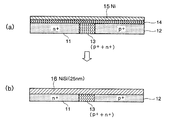
図3(a)に示すように、n+多結晶シリコン領域11とp+多結晶シリコン領域12の表層に、RTA(ラピッドサーマルアニーリング)により1000℃以上で10秒以下の活性化熱処理をほどこすことによって、不純物が高濃度で偏析した不純物偏析層14が形成される。またn+多結晶シリコン領域11とp+多結晶シリコン領域12の隣接する境界領域13では、n+不純物とp+不純物が両方ともlE20cm−3以上の高濃度でドープされ、特にこの領域の表層である不純物偏析層14にはBとP、BとAs+Pが高濃度でドープされた状態にある。
As shown in FIG. 3A, activation heat treatment is applied to the surface layers of the n +
この後、Niの金属材料膜15を7−15nmの厚さに成膜して300℃〜400℃で30秒間加熱する。この場合、図3(b)に示すように、両側の多結晶シリコン領域11,12上には、十分な厚さのNiSiの金属シリサイド膜16が形成されるものの、重複ドーピング領域となる境界領域13の表層部分には、NiSiの金属シリサイド膜の形成が十分に起きない金属シリサイド膜16aの領域が形成され、ゲート電極または配線のシート抵抗が著しく高くなるという問題がある。
Thereafter, a Ni
NiSi形成温度を600℃程度まで高くすれば、n+、p+に対してn+とp+の重なり部分でのNiSi膜厚は1.5倍程度に抑えられるが、温度が高いとNiSiが凝集して島状になったり、NiSi2というSiリッチのシリサイドに変化してSiに深く食い込んだり、孤立パターン部分では周辺のSTI上のNi膜がSi部分に集中的に入り込んでNiSiの厚みが設計以上に厚膜化するという問題がある。 If higher NiSi formation temperature to about 600 ° C., n +, NiSi film thickness in the n + and p + overlapping portion with respect to p + is suppressed to about 1.5 times, but NiSi and temperature is high Aggregates to form islands, changes to Si-rich silicide of NiSi 2 and penetrates deeply into the Si, or in the isolated pattern portion, the Ni film on the peripheral STI intensively enters the Si portion and the thickness of NiSi increases. There is a problem that the film becomes thicker than designed.
加えて、多結晶シリコンや多結晶シリコンGe表面の酸化膜を除去してからNi膜を成膜しても、この問題が解決できないことを本発明者は知得している。 In addition, the present inventor has known that this problem cannot be solved even if the Ni film is formed after removing the oxide film on the surface of polycrystalline silicon or polycrystalline silicon Ge.
これらの問題を解決するために、n+領域とp+領域が重ならないようにマスク設計上でn+とp+不純物をドープする領域をずらす方法があるが、SOCのように少量多品種の製品では、製品ごとに回路パターンが異なるため、CAD修正ワークが多くなり、場合によっては設計変更が非常に難しく対応できないという問題が生じる。 In order to solve these problems, there is a method of shifting the n + and p + impurity-doped regions in the mask design so that the n + region and the p + region do not overlap. Since products have different circuit patterns for each product, the number of CAD correction works increases, and in some cases, there is a problem that design changes are very difficult and cannot be handled.
本件発明者は、このような不具合につながる現象が、BとP、BとAs、Bと(As+P)というように、n型不純物とp型不純物が高濃度で存在する時に起こることを本発明者の行った実験により知得するに至った。 The present inventor has found that the phenomenon leading to such a failure occurs when n-type impurities and p-type impurities are present at a high concentration, such as B and P, B and As, and B and (As + P). It came to know by the experiment that the person performed.
図5、図6のグラフに、そのことを示す。 This is shown in the graphs of FIGS.
図5は6つの実験を行った結果を示しており、多結晶シリコンには総注入量として1E16cm−2を用いている。 FIG. 5 shows the results of six experiments. 1E16 cm −2 is used as the total implantation amount for polycrystalline silicon.
図からも明らかなように、B、P、Asが単独で1El6cm−2注入された多結晶シリコンの場合、シート抵抗値は約10Ω/□程度である。 As is apparent from the figure, in the case of polycrystalline silicon in which B, P, and As are independently implanted with 1E16 cm −2 , the sheet resistance value is about 10Ω / □.
これに対して、Bを5E15cm−2、Pを5El5cm−2で合計1E16cm−2注入した場合、Bを5El5cm−2、Asを5E15cm−2で合計1El6cm−2注入した場合、Bを5E15cm−2、Pを3El5cm−2、Asを2E15cm−2で合計1E16cm−2注入した場合には、いずれも30〜40Ω/□という結果になっていることを本発明者は知得した。 In contrast, the B 5E15 cm -2, if the sum 1E16 cm -2 implanted P in 5El5cm -2, the B 5El5cm -2, if the sum 1El6cm -2 implant As with 5E15 cm -2, 5E15 cm and B -2 The present inventor has found that when P is 3E15 cm −2 and As is 2E15 cm −2 and 1E16 cm −2 is injected in total, the result is 30 to 40 Ω / □.
また、総注入量を変えた実験では、図6のグラフに示すように、Si表層の総不純物濃度が4E20cm−3を超えるとNiシリサイドの厚みが薄くなり、シート抵抗値が高くなることを知得した。 Further, in the experiment in which the total implantation amount is changed, as shown in the graph of FIG. 6, it is known that when the total impurity concentration of the Si surface layer exceeds 4E20 cm −3 , the thickness of the Ni silicide is reduced and the sheet resistance value is increased. Got.
また多結晶シリコン表面には不純物が内部よりも高濃度に偏析していることも知得した。 It was also found that impurities were segregated at a higher concentration on the polycrystalline silicon surface than inside.
不純物ドーピングの後に表層に偏析した5nm以下の領域を除去するか、シリサイデーションに悪影響を与えない元素をイオン注入またはプラズマドーピングして、B−P、B−Asの結合を切れば、シリサイド形成金属がSiと反応しやすくなることも知得した。 Silicide formation is achieved by removing a region of 5 nm or less segregated on the surface layer after impurity doping, or by ion-implanting or plasma-doping an element that does not adversely affect silicidation to cut the bond of BP and B-As. It has also been found that metals easily react with Si.
本発明は上記に基づいてなされたものである。
本発明を実施するための最良の形態について、半導体基板上にMOSトランジスタ構造を形成する場合を例にとって、図面に基づき、いくつかの実施例を挙げながら説明する。ちなみに、下記実施例では、多結晶シリコンについて取り上げるが、多結晶シリコンGeを用いた実施の形態でも同様な結果が得られる。
The present invention has been made based on the above.
BEST MODE FOR CARRYING OUT THE INVENTION The best mode for carrying out the present invention will be described with reference to the accompanying drawings, taking as an example the case where a MOS transistor structure is formed on a semiconductor substrate. Incidentally, in the following examples, polycrystalline silicon is taken up, but similar results can be obtained also in an embodiment using polycrystalline silicon Ge.
また、図1(a)、図3(a)に、n+多結晶シリコン領域11、p+多結晶シリコン領域12、境界領域(p+不純物+n+不純物)13を示しているが、これらは、前述の図4で説明した工程等で製造したものである。つまり、PMOS FETとNMOS FETを並べて形成するため、n型不純物とp型不純物と交互に打ち込む。まず、n+不純物を打ち込むには、図4(b)に示すように、図中右側にマスクM1を形成しておき、p+不純物の打ち込むには、図4(c)に示すように、図中左側にマスクM2を形成しておき、この状態でそれぞれ打ち込む。これにより、マスクM1で被われていない図中左側の第1露呈部分に、n+の不純物が打ち込まれた多結晶シリコン領域12が形成され、図中右側の第2露呈部分に、p+の不純物が打ち込まれた多結晶シリコン領域11が形成され、図中中央部分としての重複露呈部分には、p+とn+の両方の不純物が打たれて、境界領域13が形成される。なお、p+とn+の打ち込む順序は、上述したのと逆に、p+を先にしても本発明は適用可能である。
FIG. 1A and FIG. 3A show an n +
(実施例1)
図1(a)、(b)、(c)は本発明の、実施例1の半導体装置の構造およびその製造方法を説明するための、断面模式図である。
Example 1
FIGS. 1A, 1B, and 1C are schematic cross-sectional views for explaining the structure of the semiconductor device of Example 1 and the manufacturing method thereof according to the present invention.
ちなみに、図1は、説明を簡単にするために、実際のトランジスタの製造に必要な、素子分離やソース・ドレイン、ウエル、チャネル、ゲート側壁スペーサーの形成プロセスを省略し、多結晶シリコンゲート電極・配線部分だけを抜き出して示しており、ゲート酸化膜も図示していない。 Incidentally, in order to simplify the explanation, FIG. 1 omits element isolation and the process of forming source / drain, well, channel, and gate sidewall spacers necessary for manufacturing an actual transistor. Only the wiring portion is extracted and shown, and the gate oxide film is not shown.
図1(a)に示すように、n+多結晶シリコン領域11とp+多結晶シリコン領域12の表層には、RTAにより、1000℃以上で10秒以下の活性化熱処理することによって、不純物が高濃度で偏析した不純物偏析層14が5nm程度の厚さに形成される。
As shown in FIG. 1A, the surface layers of the n +
またn+多結晶シリコン領域11とp+多結晶シリコン領域12が隣接する境界領域13では、n+不純物とp+不純物が両方とも、1E20cm−3以上の高濃度でドープされた状態にあり、特にこの領域の表層である不純物偏析層14(1−5nm)にはBとP、BとAs+Pが高濃度でドープされている。ここで、III族の元素としてはBの他にGa,Inを用いることができ、V族の元素としてP,Asの他にSbを用いることができる。後述の実施例2でも同様である。
In the
続いて、図1(b)に示すように、多結晶シリコン表層である不純物偏析層14を、ドライエッチングまたはウエットエッチングで除去する。
Subsequently, as shown in FIG. 1B, the
ドライエッチングではNF3+H2の混合ガスやSF6+H2の混合ガス、F2+H2の混合ガス、HFガスなどを、0.5気圧以下の圧力下で、Si基板に供給し多結晶シリコン表層である不純物偏析層14を除去する。ガス条件によってはSi基板を100℃〜300℃程度に加熱しながらガスを供給するか、ガス供給後に加熱する。
In dry etching, a mixed gas of NF 3 + H 2, a mixed gas of SF 6 + H 2, a mixed gas of F 2 + H 2 , HF gas, or the like is supplied to the Si substrate under a pressure of 0.5 atm or less. The
ウエットエッチングで行う場合には、コリンなどのアルカリ性液を用いるか、硫酸/過酸化水素水または塩酸/過酸化水素水またはアンモニア水/過酸化水素水の混合液で表層を酸化して、その酸化膜を希釈した弗酸または弗化アンモンで除去する。ウエットエッチング後のウエハの乾燥には、イソプロピルアルコールなどを用いて表層に水ガラス(Watermark)が残らないように注意する必要がある。 When performing wet etching, an alkaline solution such as choline is used, or the surface layer is oxidized with a mixed solution of sulfuric acid / hydrogen peroxide solution, hydrochloric acid / hydrogen peroxide solution, ammonia water / hydrogen peroxide solution, and the oxidation is performed. The membrane is removed with diluted hydrofluoric acid or ammonium fluoride. When drying the wafer after wet etching, care must be taken so that water glass does not remain on the surface using isopropyl alcohol or the like.
以上のように、エッチングにより、Si表層の5nm以下の厚みを除去することによって、Si表層の総不純物濃度を4E20cm−3以下に抑制できる。 As described above, the total impurity concentration of the Si surface layer can be suppressed to 4E20 cm −3 or less by removing the thickness of the Si surface layer of 5 nm or less by etching.
以上のような処理を加えることにより、Niシリサイドの厚みの薄膜化を抑制し、シート抵抗値上昇を抑制できることができる。 By applying the treatment as described above, it is possible to suppress the Ni silicide thickness from being reduced, and to suppress an increase in the sheet resistance value.
この後、Niの金属材料膜を7−15nmの厚さに成膜して、250−500℃、好ましくは、250−350℃で、30秒間の加熱を行うと、図1(c)に示すように、重複ドーピング領域となる境界領域13の表層部分でもNiSiの金属シリサイド膜16の形成が十分に起きて、所望のゲート電極または配線のシート抵抗を得ることができる。
Thereafter, a Ni metal material film having a thickness of 7 to 15 nm is formed and heated at 250 to 500 ° C., preferably 250 to 350 ° C. for 30 seconds, as shown in FIG. As described above, the NiSi
(実施例2)
図2(a)、(b)は本発明の、実施例2の半導体装置の構造およびその製造方法を説明するための、断面模式図である。
(Example 2)
2A and 2B are schematic cross-sectional views for explaining the structure of the semiconductor device of Example 2 and the manufacturing method thereof according to the present invention.
ちなみに、図2は、図1と同様に、説明の簡単のために、実際のトランジスタの製造に必要な、素子分離やソース・ドレイン、ウエル、チャネル、ゲート側壁スペーサーの形成プロセスを省略し、多結晶シリコンゲート電極・配線部分だけを抜き出して示しており、ゲート酸化膜も図示していない。 For simplicity, FIG. 2 omits the element isolation and the process of forming source / drain, well, channel, and gate sidewall spacers necessary for actual transistor fabrication, for simplicity of explanation. Only the crystalline silicon gate electrode / wiring portion is extracted, and the gate oxide film is not shown.
図2(a)で示すように、n+多結晶シリコン領域11とp+多結晶シリコン領域12の表層に、RTAにより、1000℃以上で0−10秒の活性化熱処理することによって、不純物が高濃度で偏析した不純物偏析層14を形成する。
As shown in FIG. 2A, the surface layer of the n +
またn+多結晶シリコン領域11とp+多結晶シリコン領域12の隣接する境界領域13には、n+不純物とp+不純物が、共に1E20cm−3以上の高濃度でドープされており、特にこの領域の表層である不純物偏析層14にはBとP、BとAs+Pが高濃度でドープされている。
In addition, an n + impurity and a p + impurity are both doped at a high concentration of 1E20 cm −3 or more in the
この多結晶シリコン表層にGeを10−20keVで5E14cm−2から5E15cm−2で注入する。しかる後にNiの金属材料膜15を、7−15nmの厚さに成膜して250−500℃、好ましくは、250−350℃で、30秒間の加熱を行う。これにより、図2(b)に示すように、重複ドーピング領域となる境界領域13の表層部分でも、NiSiの金属シリサイド膜16の形成が十分に起きて、所望のゲート電極または配線のシート抵抗を得ることができる。
Ge is implanted into the polycrystalline silicon surface layer at 10-20 keV at 5E14 cm −2 to 5E15 cm −2 . Thereafter, a Ni
この多結晶シリコン表層を破砕するイオン種としてはGe以外にSi、Snが有効である。 In addition to Ge, Si and Sn are effective as ion species for crushing the polycrystalline silicon surface layer.
なお、上記実施例は、半導体装置に適用されるMOSトランジスタの場合を例示したが、本発明は、トランジスタに限らず、半導体装置に組み込まれるその他の半導体素子においても同様に適用可能であることは言うまでもない。 In the above embodiment, the MOS transistor applied to the semiconductor device is exemplified. However, the present invention is not limited to the transistor, and may be applied to other semiconductor elements incorporated in the semiconductor device. Needless to say.
11 n型多結晶シリコン領域
12 p型多結晶シリコン領域
13 境界領域
14 不純物偏析層
15 金属材料膜
16、16a 金属シリサイド膜
11 n-type polycrystalline silicon region 12 p-type
Claims (5)
前記半導体層中に、不純物の導入により、p型不純物層及びn型不純物層を形成すると共にこれらの間に挟まれた位置に(p+n)型不純物層を形成し、
前記半導体層をRTAで熱処理することにより、前記p型、n型及び(p+n)型不純物層の表層に、不純物が前記半導体層内部よりも高濃度で偏析した不純物偏析層を形成し、
この不純物偏析層を除去することにより、前記半導体層の表層の総不純物濃度を低下させ、
この後、前記半導体層上に金属材料を成膜し、熱処理することによりシリサイド膜を形成する、
ことを特徴とする、半導体装置の製造方法。 A method of manufacturing a semiconductor device including forming a silicide film on a surface of a semiconductor layer,
In the semiconductor layer, by introducing impurities, a p-type impurity layer and an n-type impurity layer are formed, and a (p + n) -type impurity layer is formed at a position sandwiched therebetween,
By heat-treating the semiconductor layer with RTA, an impurity segregation layer in which impurities are segregated at a higher concentration than the inside of the semiconductor layer is formed on the surface layer of the p-type, n-type and (p + n) -type impurity layers,
By removing this impurity segregation layer, the total impurity concentration of the surface layer of the semiconductor layer is reduced,
Thereafter, a metal material is formed on the semiconductor layer, and a silicide film is formed by heat treatment.
A method for manufacturing a semiconductor device.
前記半導体層中に、不純物の導入により、p型不純物層及びn型不純物層を形成すると共にこれらの間に挟まれた位置に(p+n)型不純物層を形成し、
前記半導体層をRTAで熱処理することにより、前記p型、n型及び(p+n)型不純物層の表層に、不純物が前記半導体層内部よりも高濃度で偏析した不純物偏析層を形成し、
この後、Ge、SiまたはSnのいずれかの不純物を前記不純物偏析層中に導入することにより、前記半導体層の表層を破砕し、
この後、前記不純物偏析層上に金属材料を成膜し、熱処理することによりシリサイド膜を形成する、
ことを特徴とする、半導体装置の製造方法。 A method of manufacturing a semiconductor device including forming a silicide film on a surface of a semiconductor layer,
In the semiconductor layer, by introducing impurities, a p-type impurity layer and an n-type impurity layer are formed, and a (p + n) -type impurity layer is formed at a position sandwiched therebetween,
By heat-treating the semiconductor layer with RTA, an impurity segregation layer in which impurities are segregated at a higher concentration than the inside of the semiconductor layer is formed on the surface layer of the p-type, n-type and (p + n) -type impurity layers,
Thereafter, by introducing an impurity of Ge, Si, or Sn into the impurity segregation layer, the surface layer of the semiconductor layer is crushed,
Thereafter, a metal material is formed on the impurity segregation layer, and a silicide film is formed by heat treatment.
A method for manufacturing a semiconductor device.
前記半導体層の表面における一側を第1のマスクで被い、露呈する第1露呈部分に、前記p型及びn型の一方の不純物を導入し、次いで、前記半導体層の表面における他側を第2のマスクで被い、前記第1露呈部分と重なった重複露呈部分を含む第2露呈部分に、他方の不純物を導入することにより、
形成されることを特徴とする、請求項1又は2に記載の半導体装置の製造方法。 The p-type, n-type and (p + n) -type impurity layers are
One side of the surface of the semiconductor layer is covered with a first mask, one of the p-type and n-type impurities is introduced into the exposed first exposed portion, and then the other side of the surface of the semiconductor layer is covered By introducing the other impurity into the second exposed portion including the overlapping exposed portion that is covered with the second mask and overlapped with the first exposed portion,
The method of manufacturing a semiconductor device according to claim 1, wherein the semiconductor device is formed.
Priority Applications (5)
| Application Number | Priority Date | Filing Date | Title |
|---|---|---|---|
| JP2004381419A JP4969779B2 (en) | 2004-12-28 | 2004-12-28 | Manufacturing method of semiconductor device |
| TW094145936A TW200636860A (en) | 2004-12-28 | 2005-12-22 | Semiconductor device, wiring and their manufacturing method |
| US11/318,478 US20060160315A1 (en) | 2004-12-28 | 2005-12-28 | Semiconductor device manufacturing method, wiring and semiconductor device |
| US12/320,655 US7879723B2 (en) | 2004-12-28 | 2009-01-30 | Semiconductor device manufacturing method, wiring and semiconductor device |
| US13/340,109 US8497205B2 (en) | 2004-12-28 | 2011-12-29 | Semiconductor device manufacturing method, wiring and semiconductor device |
Applications Claiming Priority (1)
| Application Number | Priority Date | Filing Date | Title |
|---|---|---|---|
| JP2004381419A JP4969779B2 (en) | 2004-12-28 | 2004-12-28 | Manufacturing method of semiconductor device |
Related Child Applications (1)
| Application Number | Title | Priority Date | Filing Date |
|---|---|---|---|
| JP2010163016A Division JP2010267991A (en) | 2010-07-20 | 2010-07-20 | Semiconductor device and wiring |
Publications (2)
| Publication Number | Publication Date |
|---|---|
| JP2006186285A JP2006186285A (en) | 2006-07-13 |
| JP4969779B2 true JP4969779B2 (en) | 2012-07-04 |
Family
ID=36684475
Family Applications (1)
| Application Number | Title | Priority Date | Filing Date |
|---|---|---|---|
| JP2004381419A Expired - Lifetime JP4969779B2 (en) | 2004-12-28 | 2004-12-28 | Manufacturing method of semiconductor device |
Country Status (3)
| Country | Link |
|---|---|
| US (3) | US20060160315A1 (en) |
| JP (1) | JP4969779B2 (en) |
| TW (1) | TW200636860A (en) |
Families Citing this family (1)
| Publication number | Priority date | Publication date | Assignee | Title |
|---|---|---|---|---|
| JP3914114B2 (en) * | 2002-08-12 | 2007-05-16 | 株式会社東芝 | Semiconductor device and manufacturing method thereof |
Family Cites Families (41)
| Publication number | Priority date | Publication date | Assignee | Title |
|---|---|---|---|---|
| US4389257A (en) * | 1981-07-30 | 1983-06-21 | International Business Machines Corporation | Fabrication method for high conductivity, void-free polysilicon-silicide integrated circuit electrodes |
| US4803539A (en) * | 1985-03-29 | 1989-02-07 | International Business Machines Corporation | Dopant control of metal silicide formation |
| US4847213A (en) * | 1988-09-12 | 1989-07-11 | Motorola, Inc. | Process for providing isolation between CMOS devices |
| JP2895166B2 (en) * | 1990-05-31 | 1999-05-24 | キヤノン株式会社 | Method for manufacturing semiconductor device |
| JPH04119631A (en) * | 1990-09-10 | 1992-04-21 | Fujitsu Ltd | Manufacture of semiconductor device |
| JPH0590574A (en) * | 1991-09-25 | 1993-04-09 | Seiko Epson Corp | Semiconductor device |
| JP3395263B2 (en) * | 1992-07-31 | 2003-04-07 | セイコーエプソン株式会社 | Semiconductor device and manufacturing method thereof |
| JP2833468B2 (en) * | 1994-02-17 | 1998-12-09 | 日本電気株式会社 | Method for manufacturing semiconductor device |
| JP3249292B2 (en) * | 1994-04-28 | 2002-01-21 | 株式会社リコー | Complementary MIS semiconductor device with dual gate structure |
| JPH0897420A (en) * | 1994-09-29 | 1996-04-12 | Toshiba Corp | Semiconductor device and its manufacture |
| JPH09205203A (en) | 1995-03-24 | 1997-08-05 | Seiko Instr Inc | Semiconductor device and its manufacture |
| US6465295B1 (en) | 1995-03-24 | 2002-10-15 | Seiko Instruments Inc. | Method of fabricating a semiconductor device |
| JPH09199717A (en) | 1996-01-17 | 1997-07-31 | Toshiba Corp | Manufacture of semiconductor device |
| JP3734559B2 (en) * | 1996-03-15 | 2006-01-11 | 富士通株式会社 | Manufacturing method of semiconductor device |
| US6054353A (en) * | 1996-03-22 | 2000-04-25 | United Microelectronics Corporation | Short turn around time mask ROM process |
| JPH1050862A (en) | 1996-08-07 | 1998-02-20 | Mitsubishi Electric Corp | Semiconductor device |
| US6030861A (en) * | 1997-01-02 | 2000-02-29 | Texas Instruments Incorporated | Method for forming dual-gate CMOS for dynamic random access memory |
| KR100255134B1 (en) * | 1997-12-31 | 2000-05-01 | 윤종용 | Semiconductor device and method for manufacturing the same |
| JP2000068506A (en) * | 1998-08-24 | 2000-03-03 | Matsushita Electronics Industry Corp | Semiconductor device and manufacture thereof |
| TW419729B (en) | 1999-01-26 | 2001-01-21 | United Microelectronics Corp | Method of a salicide process in integrated circuit |
| JP3295931B2 (en) * | 1999-04-28 | 2002-06-24 | 日本電気株式会社 | Method for manufacturing semiconductor device |
| US20010052626A1 (en) * | 1999-09-14 | 2001-12-20 | Integrated Device Technology, Inc. | Method for fabricating dual-gate structure |
| US6800512B1 (en) * | 1999-09-16 | 2004-10-05 | Matsushita Electric Industrial Co., Ltd. | Method of forming insulating film and method of fabricating semiconductor device |
| KR100353551B1 (en) * | 2000-01-28 | 2002-09-27 | 주식회사 하이닉스반도체 | Method of forming silicide |
| US6331486B1 (en) * | 2000-03-06 | 2001-12-18 | International Business Machines Corporation | Method and structure for reduction of contact resistance of metal silicides using a metal-germanium alloy |
| JP3549193B2 (en) * | 2000-03-31 | 2004-08-04 | キヤノン販売株式会社 | Method for modifying surface on which film is formed and method for manufacturing semiconductor device |
| JP2001291780A (en) | 2000-04-06 | 2001-10-19 | Seiko Epson Corp | Method for manufacturing semiconductor device |
| JP2002076138A (en) * | 2000-08-28 | 2002-03-15 | Mitsubishi Electric Corp | Method of manufacturing semiconductor device having dual gate structure and semiconductor device manufactured by the method |
| TW558754B (en) | 2001-02-14 | 2003-10-21 | United Microelectronics Corp | Self-aligned silicide process method |
| US6812529B2 (en) * | 2001-03-15 | 2004-11-02 | Micron Technology, Inc. | Suppression of cross diffusion and gate depletion |
| JP4000256B2 (en) * | 2001-12-11 | 2007-10-31 | 富士通株式会社 | Semiconductor device and manufacturing method thereof |
| JP3607684B2 (en) | 2002-03-25 | 2005-01-05 | エルピーダメモリ株式会社 | Manufacturing method of semiconductor device |
| EP1411351A4 (en) * | 2002-06-05 | 2010-07-07 | Panasonic Corp | DEVICE FOR MEASURING AN EXTRACELLULAR POTENTIAL AND METHOD FOR MANUFACTURING THE SAME |
| US7449385B2 (en) * | 2002-07-26 | 2008-11-11 | Texas Instruments Incorporated | Gate dielectric and method |
| JP3914114B2 (en) * | 2002-08-12 | 2007-05-16 | 株式会社東芝 | Semiconductor device and manufacturing method thereof |
| JP4083507B2 (en) * | 2002-08-28 | 2008-04-30 | セイコーインスツル株式会社 | Manufacturing method of semiconductor device |
| US6787864B2 (en) * | 2002-09-30 | 2004-09-07 | Advanced Micro Devices, Inc. | Mosfets incorporating nickel germanosilicided gate and methods for their formation |
| JP3762378B2 (en) * | 2003-03-20 | 2006-04-05 | 株式会社東芝 | Semiconductor device and manufacturing method thereof |
| JP2004319592A (en) * | 2003-04-11 | 2004-11-11 | Nec Electronics Corp | Semiconductor device and its manufacturing method |
| JP2005203436A (en) * | 2004-01-13 | 2005-07-28 | Seiko Epson Corp | Semiconductor device manufacturing method and semiconductor device |
| US7338865B2 (en) * | 2004-07-23 | 2008-03-04 | Texas Instruments Incorporated | Method for manufacturing dual work function gate electrodes through local thickness-limited silicidation |
-
2004
- 2004-12-28 JP JP2004381419A patent/JP4969779B2/en not_active Expired - Lifetime
-
2005
- 2005-12-22 TW TW094145936A patent/TW200636860A/en unknown
- 2005-12-28 US US11/318,478 patent/US20060160315A1/en not_active Abandoned
-
2009
- 2009-01-30 US US12/320,655 patent/US7879723B2/en active Active
-
2011
- 2011-12-29 US US13/340,109 patent/US8497205B2/en not_active Expired - Lifetime
Also Published As
| Publication number | Publication date |
|---|---|
| TW200636860A (en) | 2006-10-16 |
| TWI304614B (en) | 2008-12-21 |
| JP2006186285A (en) | 2006-07-13 |
| US20060160315A1 (en) | 2006-07-20 |
| US7879723B2 (en) | 2011-02-01 |
| US20120164811A1 (en) | 2012-06-28 |
| US8497205B2 (en) | 2013-07-30 |
| US20090203181A1 (en) | 2009-08-13 |
Similar Documents
| Publication | Publication Date | Title |
|---|---|---|
| KR101608908B1 (en) | A transistor with embedded si/ge material having reduced offset to the channel region | |
| US6248637B1 (en) | Process for manufacturing MOS Transistors having elevated source and drain regions | |
| US7915131B2 (en) | Semiconductor device and method for fabricating the same | |
| CN100378965C (en) | Method for forming differential strain active region and strain active region thereof | |
| JP5578001B2 (en) | Manufacturing method of semiconductor device | |
| JP2007214208A (en) | Semiconductor device and manufacturing method thereof | |
| US7994591B2 (en) | Semiconductor device and method for manufacturing the same | |
| JP2002016246A (en) | Method of manufacturing MOS type semiconductor transistor | |
| JP2009111046A (en) | Semiconductor device and manufacturing method of semiconductor device | |
| JP4969779B2 (en) | Manufacturing method of semiconductor device | |
| JP3295931B2 (en) | Method for manufacturing semiconductor device | |
| CN108573873B (en) | Manufacturing method of semiconductor device | |
| JP2008047586A (en) | Semiconductor device, and its fabrication process | |
| JPH09199720A (en) | Mos type semiconductor device and its fabrication | |
| JP4167381B2 (en) | Manufacturing method of semiconductor device | |
| JPH10163130A (en) | Semiconductor device and manufacturing method thereof | |
| JP2010267991A (en) | Semiconductor device and wiring | |
| KR100549001B1 (en) | Manufacturing method of MOS transistor with complete silicide gate | |
| KR100576826B1 (en) | Nickel Salicide Process and Manufacturing Method of Semiconductor Device Using the Same | |
| JPH07153939A (en) | Semiconductor element and manufacture thereof | |
| JP2001094100A (en) | Fabrication method of semiconductor device | |
| KR100604046B1 (en) | Manufacturing Method of Semiconductor Device | |
| TWI480957B (en) | Method of fabricating n-channel metal-oxide semiconductor transistor | |
| JP3523627B2 (en) | Semiconductor device and manufacturing method thereof | |
| JPH07193235A (en) | Semiconductor device and its manufacture |
Legal Events
| Date | Code | Title | Description |
|---|---|---|---|
| A621 | Written request for application examination |
Free format text: JAPANESE INTERMEDIATE CODE: A621 Effective date: 20070927 |
|
| A977 | Report on retrieval |
Free format text: JAPANESE INTERMEDIATE CODE: A971007 Effective date: 20100127 |
|
| A131 | Notification of reasons for refusal |
Free format text: JAPANESE INTERMEDIATE CODE: A131 Effective date: 20100129 |
|
| A521 | Request for written amendment filed |
Free format text: JAPANESE INTERMEDIATE CODE: A523 Effective date: 20100330 |
|
| A02 | Decision of refusal |
Free format text: JAPANESE INTERMEDIATE CODE: A02 Effective date: 20100511 |
|
| A521 | Request for written amendment filed |
Free format text: JAPANESE INTERMEDIATE CODE: A523 Effective date: 20100720 |
|
| A911 | Transfer to examiner for re-examination before appeal (zenchi) |
Free format text: JAPANESE INTERMEDIATE CODE: A911 Effective date: 20100825 |
|
| A912 | Re-examination (zenchi) completed and case transferred to appeal board |
Free format text: JAPANESE INTERMEDIATE CODE: A912 Effective date: 20100917 |
|
| A521 | Request for written amendment filed |
Free format text: JAPANESE INTERMEDIATE CODE: A523 Effective date: 20120221 |
|
| A01 | Written decision to grant a patent or to grant a registration (utility model) |
Free format text: JAPANESE INTERMEDIATE CODE: A01 |
|
| A61 | First payment of annual fees (during grant procedure) |
Free format text: JAPANESE INTERMEDIATE CODE: A61 Effective date: 20120404 |
|
| FPAY | Renewal fee payment (event date is renewal date of database) |
Free format text: PAYMENT UNTIL: 20150413 Year of fee payment: 3 |
|
| R151 | Written notification of patent or utility model registration |
Ref document number: 4969779 Country of ref document: JP Free format text: JAPANESE INTERMEDIATE CODE: R151 |
|
| FPAY | Renewal fee payment (event date is renewal date of database) |
Free format text: PAYMENT UNTIL: 20150413 Year of fee payment: 3 |
|
| S111 | Request for change of ownership or part of ownership |
Free format text: JAPANESE INTERMEDIATE CODE: R313111 |
|
| R350 | Written notification of registration of transfer |
Free format text: JAPANESE INTERMEDIATE CODE: R350 |
|
| S111 | Request for change of ownership or part of ownership |
Free format text: JAPANESE INTERMEDIATE CODE: R313111 |
|
| R350 | Written notification of registration of transfer |
Free format text: JAPANESE INTERMEDIATE CODE: R350 |
|
| EXPY | Cancellation because of completion of term |