JP4942009B2 - Semiconductor device - Google Patents
Semiconductor device Download PDFInfo
- Publication number
- JP4942009B2 JP4942009B2 JP2004570847A JP2004570847A JP4942009B2 JP 4942009 B2 JP4942009 B2 JP 4942009B2 JP 2004570847 A JP2004570847 A JP 2004570847A JP 2004570847 A JP2004570847 A JP 2004570847A JP 4942009 B2 JP4942009 B2 JP 4942009B2
- Authority
- JP
- Japan
- Prior art keywords
- impurity concentration
- well
- transistor
- concentration distribution
- region
- Prior art date
- Legal status (The legal status is an assumption and is not a legal conclusion. Google has not performed a legal analysis and makes no representation as to the accuracy of the status listed.)
- Expired - Fee Related
Links
- 239000004065 semiconductor Substances 0.000 title claims abstract description 52
- 239000012535 impurity Substances 0.000 claims abstract description 89
- 238000009826 distribution Methods 0.000 claims abstract description 50
- 238000002955 isolation Methods 0.000 claims abstract description 13
- 239000000758 substrate Substances 0.000 claims description 31
- 238000000034 method Methods 0.000 abstract description 34
- 230000001747 exhibiting effect Effects 0.000 abstract 1
- 238000005468 ion implantation Methods 0.000 description 124
- 229920002120 photoresistant polymer Polymers 0.000 description 74
- 150000002500 ions Chemical class 0.000 description 42
- 238000004519 manufacturing process Methods 0.000 description 42
- 108091006146 Channels Proteins 0.000 description 41
- 230000001133 acceleration Effects 0.000 description 26
- 101000621511 Potato virus M (strain German) RNA silencing suppressor Proteins 0.000 description 12
- VYPSYNLAJGMNEJ-UHFFFAOYSA-N Silicium dioxide Chemical compound O=[Si]=O VYPSYNLAJGMNEJ-UHFFFAOYSA-N 0.000 description 10
- 229910052814 silicon oxide Inorganic materials 0.000 description 10
- 230000015572 biosynthetic process Effects 0.000 description 9
- 230000015556 catabolic process Effects 0.000 description 9
- 108010063256 HTLV-1 protease Proteins 0.000 description 7
- 229910052581 Si3N4 Inorganic materials 0.000 description 7
- 238000012986 modification Methods 0.000 description 7
- 230000004048 modification Effects 0.000 description 7
- HQVNEWCFYHHQES-UHFFFAOYSA-N silicon nitride Chemical compound N12[Si]34N5[Si]62N3[Si]51N64 HQVNEWCFYHHQES-UHFFFAOYSA-N 0.000 description 7
- 101000761576 Homo sapiens Serine/threonine-protein phosphatase 2A 55 kDa regulatory subunit B gamma isoform Proteins 0.000 description 6
- 101000831940 Homo sapiens Stathmin Proteins 0.000 description 6
- 102100024926 Serine/threonine-protein phosphatase 2A 55 kDa regulatory subunit B gamma isoform Human genes 0.000 description 6
- 102100024237 Stathmin Human genes 0.000 description 6
- 229910021420 polycrystalline silicon Inorganic materials 0.000 description 6
- 101710204573 Protein phosphatase PP2A regulatory subunit B Proteins 0.000 description 5
- 125000006850 spacer group Chemical group 0.000 description 5
- 108010075750 P-Type Calcium Channels Proteins 0.000 description 4
- 230000007423 decrease Effects 0.000 description 4
- 238000001020 plasma etching Methods 0.000 description 4
- 229920005591 polysilicon Polymers 0.000 description 4
- XUIMIQQOPSSXEZ-UHFFFAOYSA-N Silicon Chemical compound [Si] XUIMIQQOPSSXEZ-UHFFFAOYSA-N 0.000 description 3
- 238000005530 etching Methods 0.000 description 3
- 229910052710 silicon Inorganic materials 0.000 description 3
- 239000010703 silicon Substances 0.000 description 3
- 101100441251 Arabidopsis thaliana CSP2 gene Proteins 0.000 description 2
- ZOXJGFHDIHLPTG-UHFFFAOYSA-N Boron Chemical compound [B] ZOXJGFHDIHLPTG-UHFFFAOYSA-N 0.000 description 2
- 102100027557 Calcipressin-1 Human genes 0.000 description 2
- 101100247605 Homo sapiens RCAN1 gene Proteins 0.000 description 2
- 101001135826 Homo sapiens Serine/threonine-protein phosphatase 2A activator Proteins 0.000 description 2
- 101000614399 Homo sapiens Serine/threonine-protein phosphatase 2A regulatory subunit B'' subunit beta Proteins 0.000 description 2
- 108090000699 N-Type Calcium Channels Proteins 0.000 description 2
- 102000004129 N-Type Calcium Channels Human genes 0.000 description 2
- 102100036782 Serine/threonine-protein phosphatase 2A activator Human genes 0.000 description 2
- 102100040471 Serine/threonine-protein phosphatase 2A regulatory subunit B'' subunit beta Human genes 0.000 description 2
- 229910021417 amorphous silicon Inorganic materials 0.000 description 2
- 229910052796 boron Inorganic materials 0.000 description 2
- 101150064416 csp1 gene Proteins 0.000 description 2
- 230000006870 function Effects 0.000 description 2
- 238000002513 implantation Methods 0.000 description 2
- 239000010410 layer Substances 0.000 description 2
- 230000003647 oxidation Effects 0.000 description 2
- 238000007254 oxidation reaction Methods 0.000 description 2
- 230000003071 parasitic effect Effects 0.000 description 2
- 101100222091 Arabidopsis thaliana CSP3 gene Proteins 0.000 description 1
- OAICVXFJPJFONN-UHFFFAOYSA-N Phosphorus Chemical compound [P] OAICVXFJPJFONN-UHFFFAOYSA-N 0.000 description 1
- 229910052785 arsenic Inorganic materials 0.000 description 1
- RQNWIZPPADIBDY-UHFFFAOYSA-N arsenic atom Chemical compound [As] RQNWIZPPADIBDY-UHFFFAOYSA-N 0.000 description 1
- 230000003247 decreasing effect Effects 0.000 description 1
- 238000013461 design Methods 0.000 description 1
- 238000011161 development Methods 0.000 description 1
- 238000010438 heat treatment Methods 0.000 description 1
- 239000012212 insulator Substances 0.000 description 1
- 230000010354 integration Effects 0.000 description 1
- 239000011229 interlayer Substances 0.000 description 1
- 238000000059 patterning Methods 0.000 description 1
- 229910052698 phosphorus Inorganic materials 0.000 description 1
- 239000011574 phosphorus Substances 0.000 description 1
- 238000000206 photolithography Methods 0.000 description 1
- 238000005268 plasma chemical vapour deposition Methods 0.000 description 1
- 238000010561 standard procedure Methods 0.000 description 1
- 238000002230 thermal chemical vapour deposition Methods 0.000 description 1
Images


Classifications
-
- H—ELECTRICITY
- H10—SEMICONDUCTOR DEVICES; ELECTRIC SOLID-STATE DEVICES NOT OTHERWISE PROVIDED FOR
- H10D—INORGANIC ELECTRIC SEMICONDUCTOR DEVICES
- H10D84/00—Integrated devices formed in or on semiconductor substrates that comprise only semiconducting layers, e.g. on Si wafers or on GaAs-on-Si wafers
- H10D84/01—Manufacture or treatment
- H10D84/0123—Integrating together multiple components covered by H10D12/00 or H10D30/00, e.g. integrating multiple IGBTs
- H10D84/0126—Integrating together multiple components covered by H10D12/00 or H10D30/00, e.g. integrating multiple IGBTs the components including insulated gates, e.g. IGFETs
- H10D84/0128—Manufacturing their channels
-
- H—ELECTRICITY
- H10—SEMICONDUCTOR DEVICES; ELECTRIC SOLID-STATE DEVICES NOT OTHERWISE PROVIDED FOR
- H10D—INORGANIC ELECTRIC SEMICONDUCTOR DEVICES
- H10D84/00—Integrated devices formed in or on semiconductor substrates that comprise only semiconducting layers, e.g. on Si wafers or on GaAs-on-Si wafers
- H10D84/01—Manufacture or treatment
- H10D84/0123—Integrating together multiple components covered by H10D12/00 or H10D30/00, e.g. integrating multiple IGBTs
- H10D84/0126—Integrating together multiple components covered by H10D12/00 or H10D30/00, e.g. integrating multiple IGBTs the components including insulated gates, e.g. IGFETs
- H10D84/0135—Manufacturing their gate conductors
- H10D84/0142—Manufacturing their gate conductors the gate conductors having different shapes or dimensions
-
- H—ELECTRICITY
- H10—SEMICONDUCTOR DEVICES; ELECTRIC SOLID-STATE DEVICES NOT OTHERWISE PROVIDED FOR
- H10D—INORGANIC ELECTRIC SEMICONDUCTOR DEVICES
- H10D84/00—Integrated devices formed in or on semiconductor substrates that comprise only semiconducting layers, e.g. on Si wafers or on GaAs-on-Si wafers
- H10D84/01—Manufacture or treatment
- H10D84/0123—Integrating together multiple components covered by H10D12/00 or H10D30/00, e.g. integrating multiple IGBTs
- H10D84/0126—Integrating together multiple components covered by H10D12/00 or H10D30/00, e.g. integrating multiple IGBTs the components including insulated gates, e.g. IGFETs
- H10D84/0156—Manufacturing their doped wells
-
- H—ELECTRICITY
- H10—SEMICONDUCTOR DEVICES; ELECTRIC SOLID-STATE DEVICES NOT OTHERWISE PROVIDED FOR
- H10D—INORGANIC ELECTRIC SEMICONDUCTOR DEVICES
- H10D84/00—Integrated devices formed in or on semiconductor substrates that comprise only semiconducting layers, e.g. on Si wafers or on GaAs-on-Si wafers
- H10D84/01—Manufacture or treatment
- H10D84/0123—Integrating together multiple components covered by H10D12/00 or H10D30/00, e.g. integrating multiple IGBTs
- H10D84/0126—Integrating together multiple components covered by H10D12/00 or H10D30/00, e.g. integrating multiple IGBTs the components including insulated gates, e.g. IGFETs
- H10D84/0165—Integrating together multiple components covered by H10D12/00 or H10D30/00, e.g. integrating multiple IGBTs the components including insulated gates, e.g. IGFETs the components including complementary IGFETs, e.g. CMOS devices
- H10D84/0167—Manufacturing their channels
-
- H—ELECTRICITY
- H10—SEMICONDUCTOR DEVICES; ELECTRIC SOLID-STATE DEVICES NOT OTHERWISE PROVIDED FOR
- H10D—INORGANIC ELECTRIC SEMICONDUCTOR DEVICES
- H10D84/00—Integrated devices formed in or on semiconductor substrates that comprise only semiconducting layers, e.g. on Si wafers or on GaAs-on-Si wafers
- H10D84/01—Manufacture or treatment
- H10D84/0123—Integrating together multiple components covered by H10D12/00 or H10D30/00, e.g. integrating multiple IGBTs
- H10D84/0126—Integrating together multiple components covered by H10D12/00 or H10D30/00, e.g. integrating multiple IGBTs the components including insulated gates, e.g. IGFETs
- H10D84/0165—Integrating together multiple components covered by H10D12/00 or H10D30/00, e.g. integrating multiple IGBTs the components including insulated gates, e.g. IGFETs the components including complementary IGFETs, e.g. CMOS devices
- H10D84/0181—Manufacturing their gate insulating layers
-
- H—ELECTRICITY
- H10—SEMICONDUCTOR DEVICES; ELECTRIC SOLID-STATE DEVICES NOT OTHERWISE PROVIDED FOR
- H10D—INORGANIC ELECTRIC SEMICONDUCTOR DEVICES
- H10D84/00—Integrated devices formed in or on semiconductor substrates that comprise only semiconducting layers, e.g. on Si wafers or on GaAs-on-Si wafers
- H10D84/01—Manufacture or treatment
- H10D84/0123—Integrating together multiple components covered by H10D12/00 or H10D30/00, e.g. integrating multiple IGBTs
- H10D84/0126—Integrating together multiple components covered by H10D12/00 or H10D30/00, e.g. integrating multiple IGBTs the components including insulated gates, e.g. IGFETs
- H10D84/0165—Integrating together multiple components covered by H10D12/00 or H10D30/00, e.g. integrating multiple IGBTs the components including insulated gates, e.g. IGFETs the components including complementary IGFETs, e.g. CMOS devices
- H10D84/0188—Manufacturing their isolation regions
-
- H—ELECTRICITY
- H10—SEMICONDUCTOR DEVICES; ELECTRIC SOLID-STATE DEVICES NOT OTHERWISE PROVIDED FOR
- H10D—INORGANIC ELECTRIC SEMICONDUCTOR DEVICES
- H10D84/00—Integrated devices formed in or on semiconductor substrates that comprise only semiconducting layers, e.g. on Si wafers or on GaAs-on-Si wafers
- H10D84/01—Manufacture or treatment
- H10D84/0123—Integrating together multiple components covered by H10D12/00 or H10D30/00, e.g. integrating multiple IGBTs
- H10D84/0126—Integrating together multiple components covered by H10D12/00 or H10D30/00, e.g. integrating multiple IGBTs the components including insulated gates, e.g. IGFETs
- H10D84/0165—Integrating together multiple components covered by H10D12/00 or H10D30/00, e.g. integrating multiple IGBTs the components including insulated gates, e.g. IGFETs the components including complementary IGFETs, e.g. CMOS devices
- H10D84/0191—Manufacturing their doped wells
-
- H—ELECTRICITY
- H10—SEMICONDUCTOR DEVICES; ELECTRIC SOLID-STATE DEVICES NOT OTHERWISE PROVIDED FOR
- H10D—INORGANIC ELECTRIC SEMICONDUCTOR DEVICES
- H10D84/00—Integrated devices formed in or on semiconductor substrates that comprise only semiconducting layers, e.g. on Si wafers or on GaAs-on-Si wafers
- H10D84/01—Manufacture or treatment
- H10D84/02—Manufacture or treatment characterised by using material-based technologies
- H10D84/03—Manufacture or treatment characterised by using material-based technologies using Group IV technology, e.g. silicon technology or silicon-carbide [SiC] technology
- H10D84/038—Manufacture or treatment characterised by using material-based technologies using Group IV technology, e.g. silicon technology or silicon-carbide [SiC] technology using silicon technology, e.g. SiGe
Landscapes
- Metal-Oxide And Bipolar Metal-Oxide Semiconductor Integrated Circuits (AREA)
- Non-Volatile Memory (AREA)
- Semiconductor Memories (AREA)
Abstract
Description
本発明は、半導体装置とその製造方法に関し、特に複数の電圧で動作する半導体装置とその製造方法に関する。 The present invention relates to a semiconductor device and a manufacturing method thereof, and more particularly to a semiconductor device that operates at a plurality of voltages and a manufacturing method thereof.
半導体集積回路装置(IC)の高集積化と共にICの構成要素であるトランジスタは微細化される。トランジスタの微細化に伴って、動作電圧は低下する。システムオンチップにおいては、低電圧動作の論理回路と高電圧動作のフラッシュメモリ駆動回路を含むフラッシュメモリ回路のような異種回路を混載する要請も強い。これを実現するには、低電圧動作の論理回路と高電圧動作のフラッシュメモリ駆動回路とを同一半導体基板上に集積化することが必要となる。 As semiconductor integrated circuit devices (ICs) are highly integrated, transistors that are components of ICs are miniaturized. With the miniaturization of transistors, the operating voltage decreases. In a system-on-chip, there is a strong demand for mounting different types of circuits such as a flash memory circuit including a low-voltage operation logic circuit and a high-voltage operation flash memory drive circuit. In order to realize this, it is necessary to integrate a low-voltage operation logic circuit and a high-voltage operation flash memory drive circuit on the same semiconductor substrate.
CMOS回路を構成する場合は、高電圧および低電圧で動作するnチャネルトランジスタと高電圧および低電圧で動作するpチャネルトランジスタとを形成することとなる。 When a CMOS circuit is configured, an n-channel transistor that operates at a high voltage and a low voltage and a p-channel transistor that operates at a high voltage and a low voltage are formed.
FIG.11A〜11Fは、このような半導体装置の典形的な製造方法を示す。 FIG. Reference numerals 11A to 11F show typical manufacturing methods of such a semiconductor device.
FIG.11Aに示すように、半導体基板101の表面に、周知の方法により絶縁膜を埋め込んだ浅い素子分離溝102(シャロートレンチアイソレーション、STI)を形成する。図には、STIで画定された4つの活性領域が示されている。図中左側の2つの活性領域には、低電圧(LV)用の薄いゲート絶縁膜と高電圧(HV)用の厚いゲート絶縁膜とを有するnチャネルMOSトランジスタN−LV、N−HVを形成する。
FIG. As shown in FIG. 11A, a shallow element isolation trench 102 (shallow trench isolation, STI) in which an insulating film is embedded is formed on the surface of the
図中右側の2つの活性領域には、低電圧(LV)用の薄いゲート絶縁膜と高電圧(HV)用の厚いゲート絶縁膜を有する2つのpチャネルMOSトランジスタP−LV、P−HVを形成する。 In the two active regions on the right side of the figure, two p-channel MOS transistors P-LV and P-HV having a thin gate insulating film for low voltage (LV) and a thick gate insulating film for high voltage (HV) are provided. Form.
先ず、nチャネルMOSトランジスタ領域に開口を有するホトレジストマスクPR51を形成し、p型ウェルWPを形成するp型不純物のイオン注入、素子分離領域下にチャネルストップ領域CSPを形成するp型不純物のイオン注入、及び厚い絶縁膜を有するトランジスタの閾値Vtを所望の値に設定するためのp型不純物のイオン注入Vt1を行なう。その後、ホトレジストマスクPR51は除去する。 First, a photoresist mask PR51 having an opening in the n-channel MOS transistor region is formed, p-type impurity ion implantation for forming the p-type well WP, and p-type impurity ion implantation for forming the channel stop region CSP under the element isolation region. And p-type impurity ion implantation Vt1 for setting the threshold value Vt of the transistor having a thick insulating film to a desired value. Thereafter, the photoresist mask PR51 is removed.
FIG.11Bに示すように、pチャネルMOSトランジスタ領域に開口を有するホトレジストマスクPR52を形成し、pチャネルMOSトランジスタ領域にn型ウェルWNを形成するn型不純物のイオン注入、素子分離領域下方にチャネルストップ領域CSNを形成するためのn型不純物のイオン注入及び厚い絶縁膜を有するpチャネルMOSトランジスタの閾値Vtを制御するためのn型不純物のイオン注入Vt2を行なう。その後ホトレジストマスクPR52は除去する。 FIG. 11B, a photoresist mask PR52 having an opening in the p-channel MOS transistor region is formed, n-type impurity ions are implanted to form an n-type well WN in the p-channel MOS transistor region, and a channel stop region is formed below the element isolation region. N-type impurity ion implantation for forming CSN and n-type impurity ion implantation Vt2 for controlling the threshold value Vt of a p-channel MOS transistor having a thick insulating film are performed. Thereafter, the photoresist mask PR52 is removed.
以上のイオン注入では、厚いゲート絶縁膜を有するトランジスタ領域N−HV、P−HVでは閾値制御が行なわれたが、薄いゲート絶縁膜を有するトランジスタ領域N−LV、P−LVにおいては閾値制御用のイオン注入は不十分である。 In the above ion implantation, the threshold value control is performed in the transistor regions N-HV and P-HV having a thick gate insulating film, but the threshold value control is performed in the transistor regions N-LV and P-LV having a thin gate insulating film. The ion implantation is insufficient.
FIG.11Cに示すように、薄いゲート絶縁膜を有するnチャネルMOSトランジスタ領域N−LVに開口を有するホトレジストマスクPR53を形成し、薄いゲート絶縁膜を形成するnチャネルMOSトランジスタ領域N−LVの閾値電圧を調整するためp型不純物の追加イオン注入Vt3を行なう。その後ホトレジストマスクPR53は除去する。 FIG. 11C, a photoresist mask PR53 having an opening is formed in the n-channel MOS transistor region N-LV having a thin gate insulating film, and the threshold voltage of the n-channel MOS transistor region N-LV forming the thin gate insulating film is set. In order to adjust, additional ion implantation Vt3 of p-type impurities is performed. Thereafter, the photoresist mask PR53 is removed.
FIG.11Dに示すように、薄いゲート絶縁膜を形成するpチャネルMOSトランジスタ領域P−LVに開口を有するホトレジストマスクPR54を形成し、薄いゲート絶縁膜を形成するpチャネルMOSトランジスタ領域P−LVに閾値電圧を制御するためのn型不純物の追加イオン注入Vt4を行なう。その後ホトレジストマスクPR54は除去する。次に、半導体基板全面に厚いゲート絶縁膜GI1を形成する。 FIG. 11D, a photoresist mask PR54 having an opening is formed in the p-channel MOS transistor region P-LV for forming a thin gate insulating film, and a threshold voltage is applied to the p-channel MOS transistor region P-LV for forming a thin gate insulating film. An additional ion implantation Vt4 of n-type impurities for controlling the above is performed. Thereafter, the photoresist mask PR54 is removed. Next, a thick gate insulating film GI1 is formed on the entire surface of the semiconductor substrate.
FIG.11Eに示すように、成長したゲート絶縁膜の上に厚いゲート絶縁膜を有するトランジスタ領域を覆うホトレジストマスクPR55を形成し、薄いゲート絶縁膜を有するトランジスタ領域を露出する.ホトレジストマスクPR55をエッチングマスクとし、ゲート絶縁膜GI1を除去する。その後ホトレジストマスクPR55は除去する。 FIG. As shown in FIG. 11E, a photoresist mask PR55 covering the transistor region having the thick gate insulating film is formed on the grown gate insulating film, and the transistor region having the thin gate insulating film is exposed. The gate insulating film GI1 is removed using the photoresist mask PR55 as an etching mask. Thereafter, the photoresist mask PR55 is removed.
半導体基板上に薄いゲート絶縁膜を形成すると、厚いゲート絶縁膜が除去された領域に薄いゲート絶縁膜GI2が形成される。このようにして、厚いゲート絶縁膜GI1と薄いゲート絶縁膜GI2とが形成される。 When the thin gate insulating film is formed on the semiconductor substrate, the thin gate insulating film GI2 is formed in the region where the thick gate insulating film is removed. In this way, a thick gate insulating film GI1 and a thin gate insulating film GI2 are formed.
FIG.11Fに示すように、ゲート絶縁膜上に多結晶シリコンのゲート電極層を形成し、パターニングして、ゲート電極Gを形成する。ゲート電極をマスクとしてソース/ドレイン領域のエクステンション部のイオン注入を行なう。酸化シリコン等のサイドウォールスペーサを形成した後、高濃度ソース/ドレイン領域のイオン注入を行なう。nチャネルMOSトランジスタ及びpチャネルMOSトランジスタのイオン注入は、それぞれレジストマスクを用いて選択的に行なう。 FIG. As shown in FIG. 11F, a gate electrode layer of polycrystalline silicon is formed on the gate insulating film and patterned to form the gate electrode G. Using the gate electrode as a mask, ion implantation of the extension portion of the source / drain region is performed. After sidewall spacers such as silicon oxide are formed, high concentration source / drain regions are ion-implanted. Ion implantation of the n-channel MOS transistor and the p-channel MOS transistor is selectively performed using a resist mask.
このようにして、FIG.11Fに示すようなCMOS半導体装置が形成される。以上説明した製造方法によれば、ゲート絶縁膜の形成以外に、ウェルおよび閾値Vt制御のために4枚のマスクを用い、8回のイオン注入を行なっている。複雑な製造工程は、製造コストの増大及び歩留りの低下につながる。製造工程を簡略化することが望まれる。 In this way, FIG. A CMOS semiconductor device as shown in 11F is formed. According to the manufacturing method described above, in addition to the formation of the gate insulating film, ion implantation is performed 8 times using four masks for controlling the well and threshold value Vt. A complicated manufacturing process leads to an increase in manufacturing cost and a decrease in yield. It is desirable to simplify the manufacturing process.
特開平11−40004は、工程数を減少した半導体装置の製造方法を提案する。このような、工程数を減少させた半導体装置の製造方法を以下に説明する。 Japanese Patent Laid-Open No. 11-40004 proposes a method of manufacturing a semiconductor device with a reduced number of processes. A method for manufacturing such a semiconductor device with a reduced number of processes will be described below.
FIG.12Aに示すように、FIG.11A同様に、シリコン基板101に素子分離領域102により4つの活性領域N−LV、N−HV、P−LV、P−HVを画定する。nチャネルトランジスタ領域に開口を有するホトレジストマスクPR51を形成し、nチャネルMOSトランジスタ領域に3回のイオン注入を行ない、p型ウェルWP、p型チャネルストップ領域CSP、p型閾値調整領域VtPを形成する。
FIG. As shown in FIG. Similarly to 11A, four active regions N-LV, N-HV, P-LV, and P-HV are defined on the
閾値調整用のイオン注入の濃度は、薄いゲート絶縁膜を有するトランジスタN−LVに適した値とする。この濃度は、厚いゲート絶縁膜を有するnチャネルMOSトランジスタN−HVの閾値調整用不純物イオン注入としては高すぎる濃度である。その後ホトレジストマスクPR51は除去する。 The concentration of ion implantation for threshold adjustment is set to a value suitable for the transistor N-LV having a thin gate insulating film. This concentration is too high for the threshold ion adjusting impurity ion implantation of the n-channel MOS transistor N-HV having a thick gate insulating film. Thereafter, the photoresist mask PR51 is removed.
FIG.12Bに示すように、pチャネルMOSトランジスタ領域に開口を有するホトレジストマスクPR52を形成し、pチャネルMOSトランジスタ領域にn型ウェルWN、n型チャネルストップ領域CSN、n型閾値調整領域VtNを形成するためのn型不純物をイオン注入する。 FIG. As shown in FIG. 12B, a photoresist mask PR52 having an opening in the p-channel MOS transistor region is formed, and an n-type well WN, an n-type channel stop region CSN, and an n-type threshold adjustment region VtN are formed in the p-channel MOS transistor region. N-type impurities are ion-implanted.
閾値調整用イオン注入の濃度は、厚いゲート絶縁膜を有するpチャネルMOSトランジスタP−HVに適した濃度とする。この濃度は、薄いゲート絶縁膜を有するpチャネルMOSトランジスタP−LVには不足する濃度である。ホトレジストマスクPR52はその後除去する。 The concentration of the threshold adjustment ion implantation is set to a concentration suitable for the p-channel MOS transistor P-HV having a thick gate insulating film. This concentration is insufficient for a p-channel MOS transistor P-LV having a thin gate insulating film. Thereafter, the photoresist mask PR52 is removed.
FIG.12Cに示すように、厚いゲート絶縁膜を形成するnチャネルMOSトランジスタ領域N−HV及び薄いゲート絶縁膜を形成するpチャネルMOSトランジスタ領域P−LVに開口を有するホトレジストマスクPR56を形成し、n型不純物を追加的にイオン注入する。薄いゲート絶縁膜を形成するpチャネルMOSトランジスタ領域P−LVにおいては、2回のn型不純物のイオン注入により、所望の不純物濃度が得られ、閾値が適性に調整される。 FIG. As shown in FIG. 12C, a photoresist mask PR56 having an opening is formed in the n-channel MOS transistor region N-HV for forming a thick gate insulating film and the p-channel MOS transistor region P-LV for forming a thin gate insulating film. Impurities are additionally ion-implanted. In the p-channel MOS transistor region P-LV in which a thin gate insulating film is formed, a desired impurity concentration is obtained by ion implantation of n-type impurities twice, and the threshold value is adjusted appropriately.
厚いゲート絶縁膜を有するnチャネルMOSトランジスタ領域N−HVにおいては、始めにイオン注入された高すぎるp型不純物濃度が、追加的にイオン注入されたn型不純物のイオン注入により補償され、不純物濃度が低下する。その後ホトレジストマスクPR56は除去する。 In the n-channel MOS transistor region N-HV having a thick gate insulating film, the excessively high p-type impurity concentration initially ion-implanted is compensated by the ion implantation of the additionally ion-implanted n-type impurity. Decreases. Thereafter, the photoresist mask PR56 is removed.
FIG.12Dに示すように、厚いゲート絶縁膜GI1を形成する。厚いゲート絶縁膜を有するトランジスタを覆うホトレジストマスクPR55をエッチングマスクとし、薄いゲート絶縁膜を形成する領域の厚いゲート絶縁膜を除去する。その後ホトレジストマスクPR55を除去し、薄いゲート絶縁膜GI2を形成する。 FIG. As shown in 12D, a thick gate insulating film GI1 is formed. Using the photoresist mask PR55 covering the transistor having a thick gate insulating film as an etching mask, the thick gate insulating film in the region where the thin gate insulating film is formed is removed. Thereafter, the photoresist mask PR55 is removed, and a thin gate insulating film GI2 is formed.
FIG.12Eに示すように、公知の方法により、ゲート電極、ソース/ドレイン領域等を形成して半導体装置を完成する。 FIG. As shown in FIG. 12E, a gate electrode, source / drain regions, and the like are formed by a known method to complete the semiconductor device.
この方法によれば、ゲート絶縁膜の選択除去を除外すると、3回のマスク工程と7回のイオン注入によりウェル内の不純物濃度分布が形成されている。FIG.11A〜11Dに示す工程と比べ、マスクが1枚減少し、イオン注入が1回減少している。 According to this method, except for the selective removal of the gate insulating film, the impurity concentration distribution in the well is formed by three mask processes and seven ion implantations. FIG. Compared to the steps shown in 11A to 11D, the number of masks is reduced by one, and ion implantation is reduced by one time.
製造工程が簡略化されたが、厚いゲート絶縁膜を有するnチャネルMOSトランジスタN−HVの閾値Vtは独立に設定できるわけではない。閾値Vtの設定について一定限度の妥協が必要となる。又、開発段階で閾値設定を変更する場合には、他のトランジスタの閾値の設定も変更する必要が生じることがある。 Although the manufacturing process has been simplified, the threshold value Vt of the n-channel MOS transistor N-HV having a thick gate insulating film cannot be set independently. A certain limit of compromise is required for setting the threshold value Vt. In addition, when changing the threshold setting at the development stage, it may be necessary to change the threshold settings of other transistors.
このように、多電圧を扱う複数種類のトランジスタを製造しようとすると、工程数が多くなりやすい。工程数を削減する製造法を採用しようとすると、新たな問題が生じ易い。多電圧で動作し、かつ簡略化された製造方法で製造することのできる半導体装置が望まれる。 As described above, when a plurality of types of transistors that handle multiple voltages are to be manufactured, the number of processes tends to increase. If it is going to employ | adopt the manufacturing method which reduces the number of processes, a new problem will arise easily. A semiconductor device that operates at multiple voltages and can be manufactured by a simplified manufacturing method is desired.
本発明の目的は、少ない製造工程数で製造することのできる、所望の特性を果たす複数種類のトランジスタを有する半導体装置を提供することである。 An object of the present invention is to provide a semiconductor device having a plurality of types of transistors that can be manufactured with a small number of manufacturing steps and have desired characteristics.
本発明の一観点によれば、半導体基板の表面から第1の深さ位置に達するように形成された素子分離領域と、前記半導体基板に形成された第1導電型の第1および第2のウェルと、前記第1のウェルに形成され、第1の厚さのゲート絶縁膜と、前記第1導電型と逆の第2導電型のソース/ドレイン領域およびゲート電極とを有する第1のトランジスタと、前記第2のウェルに形成され、前記第1の厚さより薄い第2の厚さのゲート絶縁膜と、第2導電型のソース/ドレイン領域およびゲート電極とを有する第2のトランジスタと、前記半導体基板に形成された前記第1導電型の第3のウェルと、前記第3のウェルに形成され、前記第1の厚さのゲート絶縁膜と、前記第2導電型のソース/ドレイン領域およびゲート電極とを有する第3のトランジスタと、を有し、前記第1のウェルは、前記第1の深さ位置と同等又はより深い深さ位置にのみ極大値を有する第1の不純物濃度分布を有し、前記第2のウェルは、前記第1のウェルと同一の第1の不純物濃度分布に前記第1の深さ位置より浅い第2の深さ位置に極大値を有する不純物濃度分布を重ね合わせ、全体としても第2の深さ位置にも極大値を示す第2の不純物濃度分布を有し、前記第1の不純物濃度分布は、前記第1の深さ位置と同等又はより深い位置に極大値を有する第3の不純物濃度分布と、前記第1の深さ位置と同等の位置に極大値を有する第4の不純物濃度分布とを重ね合わせたものであり、前記第3のウェルは、前記第4の不純物濃度分布の極大値と等しい深さ位置に前記第4の不純物濃度分布の極大値よりも小さな極大値を有する第5の不純物濃度分布と、前記第3の不純物濃度分布とを重ね合わせた不純物濃度分布を有する半導体装置が提供される。
According to one aspect of the present invention, an element isolation region formed so as to reach a first depth position from the surface of a semiconductor substrate, and first and second conductivity types formed on the semiconductor substrate. A first transistor formed in the first well, having a first thickness gate insulating film, and a source / drain region and a gate electrode of a second conductivity type opposite to the first conductivity type; A second transistor formed in the second well and having a gate insulating film having a second thickness smaller than the first thickness, a source / drain region of a second conductivity type, and a gate electrode; A third well of the first conductivity type formed in the semiconductor substrate; a gate insulating film of the first thickness; and a source / drain region of the second conductivity type formed in the third well. And a third transistor having a gate electrode It includes a register, wherein the first well has a first impurity concentration distribution having only maximum values in the first depth position equal to or deeper than the depth position, the second well Superimposes an impurity concentration distribution having a maximum value at a second depth position shallower than the first depth position on the same first impurity concentration distribution as that of the first well, and the second as a whole. also have a second impurity concentration distribution indicating a maximum value at a depth position, wherein the first impurity concentration distribution, the third impurity having the maximum value in the first depth position equal to or deeper than A concentration distribution and a fourth impurity concentration distribution having a maximum value at a position equivalent to the first depth position are superimposed, and the third well has a fourth impurity concentration distribution. Smaller than the maximum value of the fourth impurity concentration distribution at a depth equal to the maximum value A fifth impurity concentration distribution of a semiconductor device having a third impurity concentration distribution obtained by superimposing a distribution of impurity concentration is provided having a maximum value.
FIG.1A〜1Dは、本発明の実施例による半導体装置の製造方法の主要工程を示す断面図である。 FIG. 1A to 1D are cross-sectional views illustrating main processes of a semiconductor device manufacturing method according to an embodiment of the present invention.
FIG2A〜2Dは、上述の実施例の変形例を示す断面図である。 FIGS. 2A to 2D are cross-sectional views showing modifications of the above-described embodiment.
FIG.3A〜3Eは、上述の実施例のさらに他の変形例を示す断面図である。 FIG. 3A to 3E are cross-sectional views showing still other modifications of the above-described embodiment.
FIG.4A〜4Dは、上述の実施例のさらに他の変形例を示す断面図である。 FIG. 4A to 4D are cross-sectional views showing still other modifications of the above-described embodiment.
FIG.5A〜5Fは、上述の実施例をCMOS半導体装置の製造方法に適用した半導体装置の製造方法の主要工程を示す断面図である。 FIG. 5A to 5F are cross-sectional views showing main steps of a semiconductor device manufacturing method in which the above-described embodiment is applied to a CMOS semiconductor device manufacturing method.
FIG.6A〜6Dは、FIG.5A〜5Fの製造方法により製造した各トランジスタの構成を示す平面図、表及びグラフである。 FIG. 6A-6D are shown in FIG. It is a top view, a table | surface, and a graph which show the structure of each transistor manufactured with the manufacturing method of 5A-5F.
FIG.7は、より多種類のトランジスタを有する半導体装置の構成を概略的に示す断面図である。 FIG. 7 is a cross-sectional view schematically showing a configuration of a semiconductor device having more types of transistors.
FIG.8A〜8ZCは、FIG.7に示す半導体装置の製造方法を示す断面図である。 FIG. 8A-8ZC are shown in FIG. 8 is a cross-sectional view showing a method for manufacturing the semiconductor device shown in FIG.
FIG.9A、9Bは、ポケット領域の作成を説明する断面図である。 FIG. 9A and 9B are cross-sectional views illustrating the creation of the pocket region.
FIG.10A〜10Jは、本発明の他の実施例による半導体装置の製造方法を示す断面図である。 FIG. 10A to 10J are cross-sectional views illustrating a method of manufacturing a semiconductor device according to another embodiment of the present invention.
FIG.11A〜11Fは、標準的技術により高電圧及び低電圧のCMOSトランジスタを製造する製造方法の主要工程を示す断面図である。 FIG. 11A to 11F are cross-sectional views showing the main steps of a manufacturing method for manufacturing high-voltage and low-voltage CMOS transistors using standard techniques.
FIG.12A〜12Eは、簡略化された工程で高電圧及び低電圧のCMOSトランジスタを製造する製造方法の例を示す断面図である。 FIG. 12A to 12E are cross-sectional views showing an example of a manufacturing method for manufacturing high-voltage and low-voltage CMOS transistors by a simplified process.
FIG.13は、低電圧動作の論理回路と、フラッシュメモリセル駆動用の高電圧トランジスタとを集積化した構成を概略的に示す断面図である。 FIG. 13 is a cross-sectional view schematically showing a configuration in which a logic circuit for low voltage operation and a high voltage transistor for driving a flash memory cell are integrated.
FIG.14A〜14Dは、FIG.13に示す複数種類のトランジスタを製造する製造方法の例を概略的に示す断面図である。 FIG. 14A-14D are shown in FIG. 14 is a cross-sectional view schematically showing an example of a manufacturing method for manufacturing a plurality of types of transistors shown in FIG.
FIG.15A〜15Cは、FIG.13に示す複数種類のトランジスタを製造する他の製造方法の例を示す断面図である。 FIG. 15A-15C are shown in FIG. 14 is a cross-sectional view showing an example of another manufacturing method for manufacturing a plurality of types of transistors shown in FIG.
FIG.16A〜16Cは、FIG.13に示す複数種類のトランジスタを製造するさらに他の製造方法の主要工程を示す断面図である。 FIG. 16A-16C are shown in FIG. 14 is a cross-sectional view showing the main steps of still another manufacturing method for manufacturing a plurality of types of transistors shown in FIG.
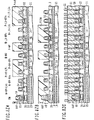
1.2V動作の論理回路に、フラッシュメモリセルを混載する場合を考察する。フラッシュメモリのプラグラム(書き込み)/消去及び読み出しには、高電圧が必要である。このような高電圧は、例えば外部から供給される1.2V電源電圧を内部回路で昇圧して発生させるのが通常である。このような低電圧から高電圧を発生させるためには、高電圧に耐えるトランジスタが必要である。さらに、リークを抑える高閾値のトランジスタと、効率良く昇圧するための低閾値のトランジスタの両方を備えることが望ましい。 Consider a case where flash memory cells are embedded in a logic circuit operating at 1.2V. High voltage is required for programming / erasing and reading of flash memory. Such a high voltage is normally generated by boosting, for example, a 1.2V power supply voltage supplied from the outside by an internal circuit. In order to generate a high voltage from such a low voltage, a transistor that can withstand the high voltage is required. Furthermore, it is desirable to include both a high threshold transistor for suppressing leakage and a low threshold transistor for efficient boosting.
FIG.13は、このような要請を反映して形成される3種類のトランジスタを示す。高電圧、低閾値トランジスタHV−LVtと、高電圧、高閾値トランジスタHV−HVtと、低電圧トランジスタLVが形成されている。高電圧トランジスタHV−LVt、HV−HVtは、例えば厚さ16nmのゲート酸化膜を有する。低電圧トランジスタLVは、例えば厚さ2nmのゲート酸化膜を有する。
FIG.
なお、高電圧トランジスタは5V動作するトランジスタに限らず、他の駆動電圧動作するトランジスタを含む場合もある。例えば、高電圧の入出力インターフェイスを備えた場合にも、待機時電流を低減する高閾値トランジスタと、動作スピードを重視する低閾値トランジスタの両方が望まれる。 Note that the high-voltage transistor is not limited to a transistor that operates at 5 V, and may include a transistor that operates at another driving voltage. For example, even when a high-voltage input / output interface is provided, both a high threshold transistor that reduces standby current and a low threshold transistor that emphasizes operating speed are desired.
このような、種々のトランジスタを集積化する場合にも適用できる簡略化された製造方法が望まれる。特に、例えば1.2V程度と動作電圧が低い場合、許容される閾値の範囲も非常に狭くなり、個々のトランジスタの閾値を独立に設定できない方法では、所望の性能を達成することが困難となる。以下、FIG.13に示すような3種類のトランジスタを製造する製造方法を検討する。 There is a desire for a simplified manufacturing method that can be applied to the integration of various transistors. In particular, when the operating voltage is as low as about 1.2 V, for example, the allowable threshold range becomes very narrow, and it is difficult to achieve the desired performance by a method in which the threshold value of each transistor cannot be set independently. . FIG. A manufacturing method for manufacturing three types of transistors as shown in FIG.
FIG.14A〜14Dは、最も標準的な製造方法の例を示す。 FIG. 14A to 14D show examples of the most standard manufacturing methods.
FIG.14Aに示すように、先ず高電圧、低閾値電圧のトランジスタHV−LVtを形成する活性領域を露出するホトレジストマスクPR61を形成し、ウェルWP1形成用p型不純物、p型チャネルストップ領域CSP1形成用p型不純物、閾値調整VtP1用p型不純物のイオン注入を計3回行なう。その後ホトレジストマスクPR61は除去する。 FIG. As shown in FIG. 14A, first, a photoresist mask PR61 that exposes an active region for forming a transistor HV-LVt having a high voltage and a low threshold voltage is formed, and a p-type impurity for forming a well WP1 and p for forming a p-type channel stop region CSP1 are formed. The ion implantation of the p-type impurity for the type impurity and the threshold adjustment VtP1 is performed three times in total. Thereafter, the photoresist mask PR61 is removed.
FIG.14Bに示すように、高電圧、高閾値電圧のトランジスタHV−HVtを形成する領域に開口を有するホトレジストマスクPR62を形成し、ウェルWP2形成用、チャネルストップ領域CSP2形成用及び閾値調整VtP2用の3種類のイオン注入を行なう。その後ホトレジストマスクPR62は除去する。 FIG. As shown in FIG. 14B, a photoresist mask PR62 having an opening in the region where the high-voltage, high-threshold-voltage transistor HV-HVt is formed is formed, and 3 for well WP2, formation of channel stop region CSP2, and threshold adjustment VtP2. Perform different types of ion implantation. Thereafter, the photoresist mask PR62 is removed.
FIG.14Cに示すように、低電圧トランジスタLV領域を露出するホトレジストマスクPR63を形成し、ウェルWP3形成用、チャネルストップ領域CSP3形成用、閾値調整VtP3用のp型不純物のイオン注入を行なう。その後ホトレジストマスクPR63は除去する。このようにして、各トランジスタ領域毎に3種類のイオン注入を行ない、その後厚いゲート酸化膜を形成し、薄いゲート酸化膜を形成する領域において一旦形成したゲート酸化膜を除去し、新たに薄いゲート酸化膜を形成する。その後、通常の方法に従い、多結晶シリコン等のゲート電極を形成する。 FIG. As shown in FIG. 14C, a photoresist mask PR63 exposing the low voltage transistor LV region is formed, and ion implantation of a p-type impurity for well WP3 formation, channel stop region CSP3 formation, and threshold adjustment VtP3 is performed. Thereafter, the photoresist mask PR63 is removed. In this way, three types of ion implantation are performed for each transistor region, and then a thick gate oxide film is formed. The gate oxide film once formed in the region where the thin gate oxide film is formed is removed, and a new thin gate is formed. An oxide film is formed. Thereafter, a gate electrode such as polycrystalline silicon is formed according to a normal method.
FIG.14Dは、このようにして形成された3種類のnチャネルMOSトランジスタを示す。3種類のトランジスタを形成するために、素子分離後ゲート絶縁膜形成前に3枚のマスクと9回のイオン注入を行なっている。工程数を減少することが望まれる。 FIG. 14D shows three types of n-channel MOS transistors formed in this manner. In order to form three types of transistors, three masks and nine ion implantations are performed after element isolation and before gate insulating film formation. It is desirable to reduce the number of steps.
FIG.15A〜15Cは、工程を簡略化した製造方法の例を示す。 FIG. 15A to 15C show examples of manufacturing methods with simplified processes.
FIG.15Aに示すように、高電圧トランジスタHV−LVt、HV−HVt領域を露出するホトレジストマスクPR71を形成し、2つのトランジスタ領域に共通に、ウェルWP1、チャネルストップ領域CSP1及び閾値調整領域VtP1形成用の3回のイオン注入を行なう。 FIG. As shown in FIG. 15A, a photoresist mask PR71 exposing the high voltage transistors HV-LVt and HV-HVt is formed, and the well WP1, the channel stop region CSP1 and the threshold adjustment region VtP1 are formed in common for the two transistor regions. Perform ion implantation three times.
なお、閾値調整用イオン注入は、低い閾値を有する高電圧トランジスタHV−LVtにおいて適正な閾値を生成する濃度である。高電圧、高閾値トランジスタHV−HVtでは、このままでは適正な閾値は得られない。 The threshold adjustment ion implantation is a concentration that generates an appropriate threshold in the high voltage transistor HV-LVt having a low threshold. In the high voltage, high threshold transistor HV-HVt, an appropriate threshold value cannot be obtained as it is.
FIG.15Bに示すように、高閾値、高電圧トランジスタHV−HVt領域を露出するレジストマスクPR62を形成し、閾値調整VtP2用の追加的イオン注入を行なう。追加されたイオン注入により閾値が適正な値まで高められる。その後、ホトレジストマスクPR62は除去する。 FIG. As shown in FIG. 15B, a resist mask PR62 exposing the high threshold voltage, high voltage transistor HV-HVt region is formed, and additional ion implantation for threshold adjustment VtP2 is performed. The threshold is raised to an appropriate value by the added ion implantation. Thereafter, the photoresist mask PR62 is removed.
FIG.15Cに示すように、低電圧トランジスタLV領域を露出するホトレジストマスクPR63を形成し、低電圧トランジスタ領域にウェルWP2、チャネルストップ領域CSP2及び閾値調整VtP3形成用の3回のイオン注入を行なう。 FIG. As shown in FIG. 15C, a photoresist mask PR63 exposing the low voltage transistor LV region is formed, and three times of ion implantation for forming the well WP2, the channel stop region CSP2, and the threshold adjustment VtP3 are performed in the low voltage transistor region.
この方法によれば、マスクは3枚と変わらないが、イオン注入の回数は7回と2回減少させることができる。 According to this method, the number of masks is not changed from three, but the number of ion implantations can be reduced to 7 times and 2 times.
FIG.16A〜16Cは、工程を簡略化した他の製造方法を示す。 FIG. 16A to 16C show other manufacturing methods with simplified processes.
FIG.16Aに示すように、3種類のトランジスタ領域を露出するホトレジストマスクPR81を形成し、全領域共通にウェルWP、チャネルストップ領域CSP及び閾値調整VtP1形成用のイオン注入を行なう。閾値調整用イオン注入は、低閾値、高電圧トランジスタHV−LVtに適合する様に調整した条件で行なう。その後ホトレジストマスクPR81は除去する。 FIG. As shown in 16A, a photoresist mask PR81 exposing three types of transistor regions is formed, and ion implantation for forming the well WP, the channel stop region CSP, and the threshold adjustment VtP1 is performed in common to all regions. Threshold adjustment ion implantation is performed under conditions adjusted to match the low threshold and high voltage transistor HV-LVt. Thereafter, the photoresist mask PR81 is removed.
FIG.16Bに示すように、高閾値、高電圧トランジスタHV−HVtを露出する開口を有するホトレジストマスクPR62を形成し、閾値調整VtP2用の追加イオン注入を行なう。レジストマスクPR62はその後除去する。 FIG. As shown in FIG. 16B, a photoresist mask PR62 having an opening exposing the high threshold voltage high voltage transistor HV-HVt is formed, and additional ion implantation for threshold adjustment VtP2 is performed. Thereafter, the resist mask PR62 is removed.
FIG.16Cに示すように、低電圧トランジスタ領域LVを露出するホトレジストマスクPR63を形成し、低電圧トランジスタの閾値調整VtP3用追加イオン注入を行なう。 FIG. As shown in 16C, a photoresist mask PR63 exposing the low voltage transistor region LV is formed, and additional ion implantation for threshold voltage adjustment VtP3 of the low voltage transistor is performed.
この方法によれば、マスクは3枚と変らないが、イオン注入の回数は5回とさらに2回減少させることができる。 According to this method, the number of masks is not changed to three, but the number of ion implantations can be further reduced to two times of five.
本発明者等の検討によれば、FIG.16A〜16Cの方法を用いた場合、1.2V動作トランジスタのための寄生トランジスタの閾値を高くするためにチャネルストップ領域形成用イオン注入濃度を大きくすると、それだけで5Vトランジスタ部の濃度が高くなりすぎる。この結果、低閾値、高電圧トランジスタHV−LVtを実現することができないことが判明した。従って、工程数の最も少ないFIG.16A−16Cの製造方法はそのままでは採用できない。 According to the study by the present inventors, FIG. When the method of 16A to 16C is used, if the ion implantation concentration for forming the channel stop region is increased in order to increase the threshold value of the parasitic transistor for the 1.2V operation transistor, the concentration of the 5V transistor portion becomes too high by itself. . As a result, it has been found that a low threshold, high voltage transistor HV-LVt cannot be realized. Therefore, the FIG. The manufacturing method of 16A-16C cannot be employed as it is.
以下、図面を参照して本発明の実施例を説明する。 Embodiments of the present invention will be described below with reference to the drawings.
FIG.1A〜1Dは、本発明の第1の実施例による半導体装置の製造方法の主要工程を示す断面図である。 FIG. 1A to 1D are cross-sectional views illustrating main processes of a method for manufacturing a semiconductor device according to a first embodiment of the present invention.
FIG.1Aに示すように、半導体基板11の1表面に、周知の方法によりシャロートレンチアイソレーション(STI)12を形成する。複数の活性領域がSTI12により画定される。以下、活性領域とそこに形成されるトランジスタとを同一の符号で示す。イオン注入とイオン注入された領域も同一符号で示す。
FIG. As shown in FIG. 1A, a shallow trench isolation (STI) 12 is formed on one surface of the
図中左の活性領域には高電圧、低閾値のトランジスタHV−LVtを形成する。図中中央の活性領域には、高電圧、高閾値のトランジスタHV−HVtを形成する。図中右側の活性領域には、低電圧トランジスタLVを形成する。 In the active region on the left in the figure, a high voltage, low threshold transistor HV-LVt is formed. In the central active region in the figure, a high voltage, high threshold transistor HV-HVt is formed. In the active region on the right side of the figure, a low voltage transistor LV is formed.
先ず、3つの活性領域を露出する開口を有するホトレジストマスクPR11を形成し、各領域でSTIと同等またはより深い深さ位置に極大値を有するウェルを形成するイオン注入14及びSTIと略同等の深さ位置に極大値を有するチャネルストップ領域を形成するイオン注入15を行なう。チャネルストップ領域15は、高電圧、低閾値トランジスタHV−LVtにおいて低閾値を生成する。その後ホトレジストマスクPR11は除去する。
First, a photoresist mask PR11 having an opening exposing three active regions is formed, and a depth substantially equal to that of STI and
なお、図においては各不純物濃度のピーク部分を領域で示したが、実際の不純物濃度分布は、より幅広い領域に広がっている。極大値の位置が多少変化しても半導体装置の動作にあまり影響しない場合も多い。「同等」、「略同等」は半導体装置の動作上同一と見なせる範囲を含む。 Although the peak portion of each impurity concentration is shown as a region in the figure, the actual impurity concentration distribution is spread over a wider region. In many cases, even if the position of the maximum value changes slightly, the operation of the semiconductor device is not significantly affected. “Equivalent” and “substantially equivalent” include ranges that can be regarded as identical in the operation of the semiconductor device.
FIG.1Bに示すように、高電圧、高閾値トランジスタHV−HVt及び低電圧トランジスタLVを露出する開口を有するホトレジストマスクPR12を形成し、高電圧、高閾値トランジスタHV−HVt又は低電圧トランジスタLVに対するフィールドトランジスタの閾値を達成するドーズ量の大きい方を追加イオン注入し、チャネルストップ領域15xを形成する。高電圧、高閾値トランジスタHV−HVtが0.5V以上であれば、通常前者を達成するドーズ量が大きく、高電圧、高閾値トランジスタHV−HVtは自由に設定できる。その後ホトレジストマスクPR12は除去する。
FIG. As shown in FIG. 1B, a photoresist mask PR12 having an opening exposing the high voltage, high threshold transistor HV-HVt and the low voltage transistor LV is formed, and a field transistor for the high voltage, high threshold transistor HV-HVt or low voltage transistor LV is formed. The ion with the larger dose amount that achieves the threshold is implanted by ion implantation to form the
FIG.1Cに示すように、低電圧トランジスタLVを開口するホトレジストマスクPR13を形成し、閾値調整用イオン注入16を行なう。その後ホトレジストマスクPR13は除去する。
FIG. As shown in FIG. 1C, a photoresist mask PR13 opening the low voltage transistor LV is formed, and threshold
以上の工程により、3枚のマスク及び4回のイオン注入により、3種類のトランジスタに対するウェル領域を形成することができる。この方法は、例えば低電圧トランジスタがゲート長0.13μm、動作電圧1.2Vというように微細化されたトランジスタであっても良好に行なうことができる。 Through the above steps, well regions for three types of transistors can be formed by three masks and four ion implantations. This method can be performed satisfactorily even if the low voltage transistor is a miniaturized transistor having a gate length of 0.13 μm and an operating voltage of 1.2 V.
なお、イオン注入する不純物をp型とすれば、nチャネルMOSトランジスタを形成することができ、イオン注入する不純物をn型とすれば、pチャネルMOSトランジスタを形成することができる。 An n-channel MOS transistor can be formed if the impurity to be ion-implanted is p-type, and a p-channel MOS transistor can be formed if the impurity to be ion-implanted is n-type.
FIG.1Dに示すように、周知の方法により、半導体基板表面上に厚いゲート酸化膜GI1及び薄いゲート酸化膜GI2を形成し、ポリシリコンによりゲート電極を形成し、エクステンション部のイオン注入を行なった後サイドウォールスペーサを形成し、高濃度ソース/ドレイン領域に対するイオン注入を行なって各トランジスタを完成する。高電圧トランジスタ17及び低電圧トランジスタ18が形成される。
FIG. As shown in FIG. 1D, after a thick gate oxide film GI1 and a thin gate oxide film GI2 are formed on the surface of the semiconductor substrate by a well-known method, a gate electrode is formed of polysilicon, and ion implantation is performed on the extension portion. Wall spacers are formed, and ions are implanted into the high concentration source / drain regions to complete each transistor. A
なお、上述の実施例においては、3つの活性領域に対し共通のウェル用イオン注入とチャネルストップ用イオン注入を行なった。ウェル用イオン注入の濃度を高く、及び/又は注入深さを浅くすることにより、高電圧、低閾値トランジスタ用のチャネルストップイオン注入を省略することも可能となる。FIG.2A〜2Dは、この変形例を示す。 In the above-described embodiment, common well ion implantation and channel stop ion implantation were performed on the three active regions. By increasing the concentration of well ion implantation and / or decreasing the implantation depth, channel stop ion implantation for a high voltage, low threshold transistor can be omitted. FIG. 2A to 2D show this modification.
FIG.2Aに示すように、3つの活性領域を露出する開口を有するホトレジストマスクPR11を形成し、3つの活性領域に対し共通のウェル領域のイオン注入14sを行なう。ウェル領域用イオン注入14sは、FIG.1Aのウェル領域用イオン注入14と比べ、深さが浅く、濃度が高く設定されている。
FIG. As shown in FIG. 2A, a photoresist mask PR11 having openings exposing the three active regions is formed, and common well region ion implantation 14s is performed on the three active regions. Well region ion implantation 14s is performed in FIG. Compared with the 1A well
このウェル用イオン注入14sにより、高電圧、低閾値トランジスタHV−LVtにおいては、チャネルストップ領域形成用イオン注入の役割が既に達成される。その後ホトレジストマスクPR11は除去する。 By this well ion implantation 14s, the role of ion implantation for forming the channel stop region is already achieved in the high voltage, low threshold transistor HV-LVt. Thereafter, the photoresist mask PR11 is removed.
FIG.2Bに示すように、高電圧、高閾値トランジスタHV−HVt及び低電圧トランジスタLVを露出する開口を有するホトレジストマスクPR12を形成、チャネルストップ領域形成用イオン注入15yを行なう。その後ホトレジストマスクPR12は除去する。
FIG. As shown in FIG. 2B, a photoresist mask PR12 having an opening exposing the high voltage, high threshold transistor HV-HVt and low voltage transistor LV is formed, and channel stop region forming
FIG.2Cに示すように、低電圧トランジスタLV領域を露出する開口を有するホトレジストマスクPR13を形成し、閾値調整用イオン注入16を行なう。その後ホトレジストマスクPR13は除去する。このようにして、3枚のマスク及び3回のイオン注入により、3種類のトランジスタを形成するウェル領域が形成される。
FIG. As shown in FIG. 2C, a photoresist mask PR13 having an opening exposing the low voltage transistor LV region is formed, and threshold
FIG.2Dに示すように、周知の方法により高電圧用絶縁ゲート電極17及び低電圧用絶縁ゲート電極18を形成する。
FIG. As shown in 2D, the high-voltage insulated
フラッシュメモリと論理回路とを混載する場合、高電圧(5V)のnチャネルMOSトランジスタは、マイナス電圧を処理するためにトリプルウェルに形成することがある。 When a flash memory and a logic circuit are mixedly mounted, a high voltage (5 V) n-channel MOS transistor may be formed in a triple well in order to process a negative voltage.
FIG.1A〜1Cの工程に、トリプルウェルを形成するイオン注入を加えた変形例を以下に説明する。 FIG. A modification in which ion implantation for forming a triple well is added to the steps 1A to 1C will be described below.
FIG.3Aに示すように、高電圧トランジスタHV−LVt、HV−HVtを露出する開口を有するホトレジストマスクPR14を形成し、n型不純物をイオン注入し、トリプルウェル用n型ウェル19を形成する。その後ホトレジストマスクPR14は除去する。 FIG. As shown in FIG. 3A, a photoresist mask PR14 having an opening exposing the high voltage transistors HV-LVt and HV-HVt is formed, and n-type impurities are ion-implanted to form an n-type well 19 for triple well. Thereafter, the photoresist mask PR14 is removed.
FIG.3Bに示すように、3種類のトランジスタ領域を露出する開口を有するホトレジストマスクPR11を形成し、3つのトランジスタ領域に対し、p型ウェルのイオン注入14、チャネルストップ領域のイオン注入15を行なう。その後ホトレジストマスクPR11は除去する。
FIG. As shown in FIG. 3B, a photoresist mask PR11 having openings for exposing three types of transistor regions is formed, and p-type
FIG.3Cに示すように、高電圧、高閾値トランジスタHV−HVt及び低電圧トランジスタLV領域を露出する開口を有するホトレジストマスクPR12を形成し、チャネルストップ領域形成用の追加イオン注入を行なう。チャネルストップ領域15xは、当初のチャネルストップ領域15よりも不純物濃度が高くなる。その後ホトレジストマスクPR12は除去する。
FIG. As shown in FIG. 3C, a photoresist mask PR12 having openings exposing the high voltage, high threshold transistor HV-HVt and low voltage transistor LV regions is formed, and additional ion implantation for forming a channel stop region is performed. The
FIG.3Dに示すように、低電圧用トランジスタLVを露出する開口を有するホトレジストマスクPR13を形成し、閾値調整用イオン注入16を行なう。その後ホトレジストマスクPR13は除去する。
FIG. As shown in 3D, a photoresist mask PR13 having an opening exposing the low voltage transistor LV is formed, and threshold
FIG.3Eに示すように、pチャネルMOSトランジスタのn型ウェル領域形成工程において用いるホトレジストマスクPR15に、nチャネルMOSトランジスタ領域の周辺に、先に形成したn型ウェル19の周辺と連続する領域に開口を形成する。 FIG. As shown in FIG. 3E, an opening is formed in the photoresist mask PR15 used in the n-type well region formation step of the p-channel MOS transistor in the region continuous with the periphery of the n-type well 19 formed in the periphery of the n-channel MOS transistor region. Form.
n型ウェルのイオン注入と共に、pチャネルトランジスタ領域のn型ウェル19の周辺部にn型領域20がイオン注入され、トリプルウェル用のn型ウェルが形成される。このようにして、トリプルウェルを有する半導体装置が形成される。
Along with the ion implantation of the n-type well, the n-
FIG.4A〜4Dは、トリプルウェルを形成する他の変形例を示す。 FIG. 4A to 4D show other modifications for forming a triple well.
FIG.4Aに示すように、高電圧トランジスタHV−LVt、HV−HVt領域を露出する開口を有するホトレジストマスクPR14を形成し、トリプルウェル用n型ウェル19、p型ウェル14H、チャネルストップ領域15Hのイオン注入を行なう。その後ホトレジストマスクPR14は除去する。
FIG. As shown in FIG. 4A, a photoresist mask PR14 having openings exposing the high voltage transistors HV-LVt and HV-HVt regions is formed, and ion implantation of the triple well n-
FIG.4Bに示すように、高電圧、高閾値トランジスタHV−HVt、低電圧トランジスタLV領域を露出する開口を有するホトレジストマスクPR12を形成し、ウェル領域用イオン注入14L及びチャネルストップ用イオン注入15Lを行なう。その後ホトレジストマスクPR12は除去する。
FIG. As shown in FIG. 4B, a photoresist mask PR12 having an opening exposing the high voltage, high threshold transistor HV-HVt and low voltage transistor LV regions is formed, and well
高電圧、高閾値トランジスタHV−HVt領域においては、2回のウェル領域用イオン注入が重畳され、不純物濃度の高いp型ウェル14Mが形成され、2回のチャネルストップ領域用イオン注入が重畳され、不純物濃度の高いチャネルストップ領域15Mが形成される。低電圧トランジスタLV用領域においては、今回のイオン注入のみにより、不純物濃度の低いウェル領域14Lと不純物濃度の低いチャネルストップ領域15Lが形成される。
In the high-voltage, high-threshold transistor HV-HVt region, two well region ion implantations are superimposed, a high impurity concentration p-
FIG.4Cに示すように、低電圧トランジスタLVを露出する開口を有するホトレジストマスクPR13を形成し、閾値調整用イオン注入16Lを行なう。低電圧トランジスタLVのみにおいて、閾値調整用イオン注入が行なわれる。
FIG. As shown in FIG. 4C, a photoresist mask PR13 having an opening exposing the low voltage transistor LV is formed, and threshold
FIG.4Dに示すように、n型ウェル形成工程において、ホトレジストマスクPR15にn型ウェル19周辺に連続するように開口を形成し、n型不純物のイオン注入20を行なう。トリプルウェルのn型ウェルが形成される。
FIG. As shown in FIG. 4D, in the n-type well formation step, an opening is formed in the photoresist mask PR15 so as to be continuous with the periphery of the n-
このようにして、FIG.3A〜3Eに比べて、マスク一枚を減少した工程数で所望の構成のウェルを有する半導体装置を形成することができる。なお、PチャネルMOS装置の場合も不純物の導電型を反転して同様の製造工程を採用することができる。 In this way, FIG. Compared to 3A to 3E, a semiconductor device having a well having a desired configuration can be formed with a reduced number of steps of one mask. In the case of a P-channel MOS device, the same manufacturing process can be adopted by inverting the impurity conductivity type.
FIG.5Aは、左側に3つのnチャネルトランジスタ領域、右側に3つのpチャネルトランジスタ領域を示す。FIG.1A−1Dに示した製造方法同様、nチャネルトランジスタ領域を露出するホトレジストマスクPR11を形成し、p型ウェル14、p型チャネルストップ15のイオン注入を行なう。
FIG. 5A shows three n-channel transistor regions on the left side and three p-channel transistor regions on the right side. FIG. Similar to the manufacturing method shown in 1A-1D, a photoresist mask PR11 exposing the n-channel transistor region is formed, and ion implantation of the p-
p型ウェル14のイオン注入は例えばB+イオンを加速エネルギ400keV、ドーズ量1.5×1013cm−2でイオン注入する。p型チャネルストップ15のイオン注入は、例えばB+イオンを加速エネルギ100keV、ドーズ量2×10¹²でイオン注入する。その後、ホトレジストマスクPR11は除去する。
In the ion implantation of the p-
FIG.5Bに示すように、高電圧、高閾値電圧nチャネルトランジスタN−HV−HVt領域及び低電圧nチャネルトランジスタN−LV領域を露出する開口を有するホトレジストマスクPR12を形成し、チャネルストップ領域形成用追加B+イオン注入を加速エネルギ100keV、ドーズ量6×1012cm−2で行なう。追加イオン注入が行なわれ、不純物濃度を増加したチャネルストップ領域15xが形成される。その後ホトレジストマスクPR12は除去する。
FIG. As shown in FIG. 5B, a photoresist mask PR12 having an opening exposing the high voltage, high threshold voltage n-channel transistor N-HV-HVt region and the low voltage n-channel transistor N-LV region is formed, and an additional channel stop region formation is formed. B + ion implantation is performed with an acceleration energy of 100 keV and a dose of 6 × 10 12 cm −2 . Additional ion implantation is performed to form a
FIG.5Cに示すように、pチャネルトランジスタ領域を露出する開口を有するホトレジストマスクPR21を形成し、n型ウェル24形成用イオン注入を行なう。P+イオンを加速エネルギ600keV、ドーズ量3.0×1013cm−2でイオン注入する。その後ホトレジストマスクPR21は除去する。
FIG. As shown in FIG. 5C, a photoresist mask PR21 having an opening exposing the p-channel transistor region is formed, and ion implantation for forming the n-
FIG.5Dに示すように、高電圧、高閾値電圧pチャネルトランジスタP−HV−HVt及び低電圧PチャネルトランジスタP−LV領域を露出する開口を有するホトレジストマスクPR22を形成し、チャネルストップ領域25形成用P+イオン注入を加速エネルギ240keV、ドーズ量5×1012cm−2で行なう。その後ホトレジストマスクPR22は除去する。
FIG. As shown in FIG. 5D, a photoresist mask PR22 having an opening exposing the high-voltage and high-threshold voltage p-channel transistors P-HV-HVt and the low-voltage P-channel transistor P-LV region is formed, and the
FIG.5Eに示すように、nチャネル低電圧トランジスタN−LVを露出する開口を有するホトレジストマスクPR13を形成し、閾値調整用p型不純物のB+イオン注入16を加速エネルギ10keV、ドーズ量4×1012cm−2で行なう。その後ホトレジストマスクPR13は除去する。
FIG. As shown in FIG. 5E, a photoresist mask PR13 having an opening exposing the n-channel low-voltage transistor N-LV is formed, B + ion implantation 16 of threshold adjustment p-type impurity is accelerated energy 10 keV, and
FIG.5Fに示すように、低電圧pチャネルトランジスタP−LVを露出する開口を有するホトレジストマスクPR23を形成し、閾値調整n型不純物のAs+イオン注入26を加速エネルギ100keV、ドーズ量5×1012cm−2で行なう。その後ホトレジストマスクPR23は除去する。
FIG. As shown in FIG. 5F, a photoresist mask PR23 having an opening exposing the low-voltage p-channel transistor P-LV is formed, the threshold adjustment n-type impurity As +
このように、6枚のマスク及び7回のイオン注入により、3種類のnチャネルMOSトランジスタ及び3種類のpチャネルMOSトランジスタのためのウェル領域を形成することができる。 In this manner, well regions for three types of n-channel MOS transistors and three types of p-channel MOS transistors can be formed by six masks and seven ion implantations.
FIG.6A−6Dは、FIG.5A〜5Fで形成されるトランジスタを説明するための図である.
FIG.6Aは、トランジスタの平面構成を概略的に示す。幅Wの矩形活性領域上に絶縁ゲート電極が形成される。絶縁ゲート電極Gの電流方向長さ(ゲート長)はLである。
FIG. 6A-6D is shown in FIG. It is a figure for demonstrating the transistor formed by 5A-5F.
FIG. 6A schematically shows a planar configuration of the transistor. An insulated gate electrode is formed on the rectangular active region having a width W. The length in the current direction (gate length) of the insulated gate electrode G is L.
FIG.6Bは、形成される各種トランジスタの特性を示す表である.低電圧nチャネルMOSトランジスタN−LVは、ゲート幅Wに対するゲート長の比L/W=0.11/1μmであり、閾値Vtは0.2Vである。nチャネル高電圧、高閾値MOSトランジスタN−HV−HVtは、L/Wが0.70/1μmであり、閾値Vtは0.6Vである。nチャネル高電圧、低閾値MOSトランジスタN−HV−LVtは、L/W比が0.70/1μmであり、閾値Vtは0.2Vである。 FIG. 6B is a table showing characteristics of various transistors formed. In the low voltage n-channel MOS transistor N-LV, the ratio of the gate length to the gate width W is L / W = 0.11 / 1 μm, and the threshold Vt is 0.2V. The n-channel high voltage, high threshold MOS transistor N-HV-HVt has an L / W of 0.70 / 1 μm and a threshold Vt of 0.6V. The n-channel high voltage, low threshold MOS transistor N-HV-LVt has an L / W ratio of 0.70 / 1 μm and a threshold Vt of 0.2V.
pチャネル低電圧MOSトランジスタP−LVは、L/Wが0.11/1μmであり、閾値Vtは−0.2Vである。pチャネル高電圧、高閾値MOSトランジスタP−HV−HVtは、L/W比が0.70/1μmであり、閾値Vtは−0.6Vである。pチャネル高電圧、低閾値MOSトランジスタP−HV−LVtは、L/W比が0.70/1μmであり、閾値Vtは−0.2Vである。 The p-channel low voltage MOS transistor P-LV has L / W of 0.11 / 1 μm and a threshold Vt of −0.2V. The p-channel high voltage, high threshold MOS transistor P-HV-HVt has an L / W ratio of 0.70 / 1 μm and a threshold Vt of −0.6V. The p-channel high voltage, low threshold MOS transistor P-HV-LVt has an L / W ratio of 0.70 / 1 μm and a threshold Vt of −0.2V.
FIG.6Cは、nチャネルMOSトランジスタ領域の不純物濃度分布を示す。横軸が基板表面からの深さ、縦軸がボロン濃度を示す。曲線N−LV、N−HV−HVt、N−HV−LVtは、それぞれnチャネル低電圧トランジスタ領域、nチャネル高電圧、高閾値トランジスタ領域、nチャネル高電圧、低閾値トランジスタ領域の不純物濃度分布を示す。 FIG. 6C shows the impurity concentration distribution of the n-channel MOS transistor region. The horizontal axis represents the depth from the substrate surface, and the vertical axis represents the boron concentration. Curves N-LV, N-HV-HVt, and N-HV-LVt show the impurity concentration distributions in the n-channel low voltage transistor region, n-channel high voltage, high threshold transistor region, n channel high voltage, and low threshold transistor region, respectively. Show.
ウェルのイオン注入は3種類のトランジスタ領域に対して共通である。素子分離領域と略同等深さのチャネルストップ領域のイオン注入はnチャネル高電圧、低閾値トランジスタ領域においては1回のみのイオン注入に対応して低く、nチャネル、高電圧、高閾値トランジスタ領域およびnチャネル低電圧トランジスタ領域においては2回のイオン注入に対応して高い。 Well ion implantation is common to the three types of transistor regions. The ion implantation of the channel stop region having a depth substantially equal to that of the element isolation region is low corresponding to one ion implantation in the n-channel high voltage, low threshold transistor region, and the n channel, high voltage, high threshold transistor region, and The n channel low voltage transistor region is high corresponding to two ion implantations.
基板のより浅い領域においては、低電圧トランジスタN−LV領域において閾値調整用イオン注入に対応して高いp型濃度ピークが形成されている。 In the shallower region of the substrate, a high p-type concentration peak is formed corresponding to the threshold adjustment ion implantation in the low-voltage transistor N-LV region.
FIG.6Dは、pチャネルMOSトランジスタ領域における不純物濃度分布を示すグラフである。横軸が基板表面からの深さ、縦軸がn型不純物濃度を示す。曲線P‐LV、P−HV−HVt、P−HV−LVtは、それぞれpチャネル低電圧トランジスタ、pチャネル高電圧、高閾値トランジスタ、pチャネル高電圧、低閾値トランジスタ領域の不純物濃度分布を示す。ウェルのイオン注入は共通である。 FIG. 6D is a graph showing an impurity concentration distribution in the p-channel MOS transistor region. The horizontal axis represents the depth from the substrate surface, and the vertical axis represents the n-type impurity concentration. Curves P-LV, P-HV-HVt, and P-HV-LVt indicate impurity concentration distributions of the p-channel low voltage transistor, the p-channel high voltage, the high threshold transistor, the p-channel high voltage, and the low threshold transistor region, respectively. Well ion implantation is common.
素子分離領域と略同等の深さのチャネルストップのイオン注入は、高電圧、高閾値トランジスタ領域、低電圧トランジスタ領域のみに行なわれ、ピーク左側の不純物濃度を高くしている。さらに浅い領域において、低電圧トランジスタ領域において閾値調整用イオン注入によりn型不純物のピークが形成されている。 Channel stop ion implantation having substantially the same depth as the element isolation region is performed only in the high voltage, high threshold transistor region, and low voltage transistor region, and the impurity concentration on the left side of the peak is increased. In the shallower region, an n-type impurity peak is formed by threshold adjustment ion implantation in the low-voltage transistor region.
次に、フラッシュメモリセルを混載した0.13μmロジックプロセスについてより詳細に説明する。 Next, a 0.13 μm logic process in which flash memory cells are embedded will be described in more detail.
FIG.7は、この半導体装置に集積化される11種類のトランジスタを列挙したものである。トランジスタFMは、フラッシュメモリセルを表わす。高電圧、低閾値トランジスタN−HV−LVtは、高耐圧で低い閾値を有するnチャネルMOSトランジスタである。高電圧、高閾値トランジスタN−HV−HVtは、高耐圧、高閾値のnチャネルMOSトランジスタである。高電圧、低閾値トランジスタP−HV−LVtは高耐圧、低閾値のpチャネルMOSトランジスタである。高電圧、高閾値トランジスタP−HV−HVtは、高耐圧、高閾値のpチャネルMOSトランジスタである。 FIG. Reference numeral 7 lists eleven types of transistors integrated in the semiconductor device. Transistor FM represents a flash memory cell. The high voltage, low threshold transistor N-HV-LVt is an n-channel MOS transistor having a high breakdown voltage and a low threshold. The high voltage, high threshold transistor N-HV-HVt is a high breakdown voltage, high threshold n-channel MOS transistor. The high voltage, low threshold transistor P-HV-LVt is a high breakdown voltage, low threshold p-channel MOS transistor. The high voltage, high threshold transistor P-HV-HVt is a high breakdown voltage, high threshold p-channel MOS transistor.
中耐圧トランジスタN−MVは、入出力インターフェイスに用いられる例えば2.5V動作のnチャネルMOSトランジスタである。中耐圧トランジスタP−MVは、入出力インターフェイスに用いられる例えば2.5V動作のpチャネルMOSトランジスタである。 The medium withstand voltage transistor N-MV is, for example, an n-channel MOS transistor operating at 2.5 V used for an input / output interface. The medium withstand voltage transistor P-MV is, for example, a 2.5-V operation p-channel MOS transistor used for an input / output interface.
低電圧、高閾値トランジスタN‐LV−HVtは、低耐圧、高閾値のnチャネルMOSトランジスタである。低電圧、低閾値トランジスタN−LV−LVtは、低耐圧、低閾値のnチャネルMOSトランジスタである。低電圧、高閾値トランジスタP‐LV‐HVtは、低耐圧、高閾値のpチャネルMOSトランジスタである。低電圧、低閾値トランジスタP−LV−LVtは、低耐圧、低閾値のpチャネルMOSトランジスタである。 The low voltage, high threshold transistor N-LV-HVt is a low breakdown voltage, high threshold n-channel MOS transistor. The low voltage, low threshold transistor N-LV-LVt is a low breakdown voltage, low threshold n-channel MOS transistor. The low voltage, high threshold transistor P-LV-HVt is a low breakdown voltage, high threshold p-channel MOS transistor. The low voltage, low threshold transistor P-LV-LVt is a low breakdown voltage, low threshold p-channel MOS transistor.
nチャネル高電圧トランジスタ及びフラッシュメモリセルは、n型ウェル19内のp型ウェル14内に形成される。nチャネルトランジスタはp型ウェル14内に形成され、pチャネルMOSトランジスタはn型ウェル24に形成される。高耐圧、低閾値pチャネルMOSトランジスタP−HV−LVt以外のトランジスタには、チャネルストップ領域15、25が形成されている。
The n-channel high voltage transistor and flash memory cell are formed in the p-type well 14 in the n-
低電圧、高閾値トランジスタN−LV−HVt、P−LV−HVtには、閾値調整用イオン注入16、26が形成されている。中電圧トランジスタN‐MV、P‐MVには、閾値調整用イオン注入37、38が形成されている。フラッシュメモリFMには、閾値調整用イオン注入36が形成されている。閾値調整用イオン注入とチャネルストップ領域とが協働してトランジスタの閾値を調整している。
Threshold
以下、FIG.7に示す半導体装置を製造する製造工程について説明する。 FIG. A manufacturing process for manufacturing the semiconductor device shown in FIG.
FIG.8Aに示すように、半導体基板11にSTI12を形成し、次いでシリコン基板表面を熱酸化し、例えば厚さ10nmの酸化シリコン膜13を形成する。
FIG. As shown in FIG. 8A, the
FIG.8Bに示すように、フラッシュメモリセルFM及び高電圧nチャネルMOSトランジスタN−HV領域を露出するホトレジストマスクPR14を形成し、n型ウェル形成用のP+イオンを加速エネルギ2MeV、ドーズ量2×1013cm−2でイオン注入する。その後レジストマスクPR14は除去する。 FIG. As shown in FIG. 8B, a photoresist mask PR14 exposing the flash memory cell FM and the high-voltage n-channel MOS transistor N-HV region is formed, and P + ions for forming an n-type well are accelerated energy 2 MeV and dose 2 × 10. Ion implantation is performed at 13 cm −2 . Thereafter, the resist mask PR14 is removed.
FIG.8Cに示すように、フラッシュメモリFM及びnチャネルMOSトランジスタ領域を露出する開口を有するホトレジストマスクPR11を形成し、p型ウェル形成用のB+イオンを加速エネルギ400keV、ドーズ量1.5×1013cm−2でイオン注入し、さらにチャネルストップ領域形成用のB+イオンを加速エネルギ100keV、ドーズ量2×1012cm−2でイオン注入する。その後レジストマスクPR11は除去する。このようにして、p型ウェル14及びチャネルストップ領域15が形成される。
FIG. As shown in FIG. 8C, a photoresist mask PR11 having an opening exposing the flash memory FM and the n-channel MOS transistor region is formed, and B + ions for forming a p-type well are accelerated at an energy of 400 keV and a dose of 1.5 × 10 13. Ion implantation is performed at cm −2 , and B + ions for forming a channel stop region are further implanted at an acceleration energy of 100 keV and a dose of 2 × 10 12 cm −2 . Thereafter, the resist mask PR11 is removed. In this way, the p-
FIG.8Dに示すように、フラッシュメモリFM及び高電圧、低閾値nチャネルトランジスタN−HV−LVtを除くnチャネルMOSトランジスタを露出するレジストマスクPR12を形成し、チャネルストップ領域形成用のB+イオンを加速エネルギ100keV、ドーズ量6×10¹²で追加的にイオン注入する。追加イオン注入をされたチャネルストップ領域15xが形成される。その後レジストマスクPR12は除去する。
FIG. As shown in FIG. 8D, a resist mask PR12 exposing the n-channel MOS transistors excluding the flash memory FM and the high-voltage, low-threshold n-channel transistors N-HV-LVt is formed, and B + ions for channel stop region formation are accelerated. Additional ion implantation is performed with an energy of 100 keV and a dose of 6 × 10 12 . A
FIG.8Eに示すように、pチャネルMOSトランジスタを露出するレジストマスクPR21を形成し、n型ウェル24形成用のP+イオンを加速エネルギ600keV、ドーズ量3.0×1013cm−2でイオン注入する。その後レジストマスクPR21は除去する。 FIG. As shown in FIG. 8E, a resist mask PR21 that exposes the p-channel MOS transistor is formed, and P + ions for forming the n-type well 24 are ion-implanted at an acceleration energy of 600 keV and a dose of 3.0 × 10 13 cm −2. . Thereafter, the resist mask PR21 is removed.
FIG.8Fに示すように、高電圧、低閾値トランジスタを除くpチャネルMOSトランジスタを露出するレジストマスクPR22を形成し、チャネルストップ領域25形成用のP+イオンを加速エネルギ240keV、ドーズ量5.0×1012cm−2でイオン注入する。その後レジストマスクPR22は除去する。
FIG. As shown in FIG. 8F, a resist mask PR22 that exposes the p-channel MOS transistor excluding the high-voltage and low-threshold transistors is formed, and P + ions for forming the
FIG.8Gに示すように、フラッシュメモリセルFMを露出するレジストマスクPR31を形成し、閾値調整用領域36を形成するB+イオンを加速エネルギ40keV、ドーズ量6×1013cm−2でイオン注入する。その後レジストマスクPR31は除去する。
FIG. As shown in FIG. 8G, a resist mask PR31 exposing the flash memory cell FM is formed, and B + ions forming the
FIG.8Hに示すように、半導体基板表面の酸化シリコン膜13をHF溶液により除去する。活性領域のシリコン表面が露出する。
FIG. As shown in 8H, the
FIG.8Iに示すように、半導体基板表面を熱酸化し、厚さ約10nmのトンネル酸化膜を成長する。トンネル酸化膜上に、厚さ約90nmの燐(P)をドープしたアモルファスシリコン膜をCVDにより堆積し、フローティングゲート31の形状にパターニングする。なお、アモルファスシリコン膜は、その後の熱処理によりポリシリコン膜に変換される。
FIG. As shown in FIG. 8I, the surface of the semiconductor substrate is thermally oxidized to grow a tunnel oxide film having a thickness of about 10 nm. On the tunnel oxide film, an amorphous silicon film doped with phosphorus (P) having a thickness of about 90 nm is deposited by CVD and patterned into the shape of the floating
フローティングゲート31を覆うように酸化シリコン膜及び窒化シリコン膜をそれぞれ5nm、10nm、CVDで堆積する。窒化シリコン膜表面を約5nm厚熱酸化して約10nm厚の酸化シリコン膜とし、全体として厚さ20nm程度のONO膜32を成長する。
A silicon oxide film and a silicon nitride film are deposited by CVD at 5 nm and 10 nm, respectively, so as to cover the floating
FIG.8Jに示すように、中電圧nチャネルMOSトランジスタN−MVを露出するレジストマスクPR32を形成し、閾値調整用領域37を形成するB+イオンを加速エネルギ30keV、ドーズ量5×1012cm−2でイオン注入する。その後レジストマスクPR32は除去する。
FIG. As shown in FIG. 8J, a resist mask PR32 exposing the medium voltage n-channel MOS transistor N-MV is formed, B + ions forming the
FIG.8Kに示すように、中電圧pチャネルMOSトランジスタP−MVを露出するレジストマスクPR33を形成し、閾値調整用領域38を形成するAs+イオンを加速エネルギ150keV、ドーズ量3×1012cm−2でイオン注入する。その後レジストマスクPR33は除去する。
FIG. As shown in FIG. 8K, a resist mask PR33 that exposes the medium voltage p-channel MOS transistor P-MV is formed, and As + ions that form the
FIG.8Lに示すように、低電圧、高閾値nチャネルトランジスタN−LV−HVt領域を露出するレジストマスクPR13を形成し、閾値調整用領域16を形成するB+イオンを加速エネルギ10keV、ドーズ量5×1012cm−2でイオン注入する。その後レジストマスクPR13は除去する。
FIG. As shown in FIG. 8L, a resist mask PR13 exposing the low-voltage, high-threshold n-channel transistor N-LV-HVt region is formed, B + ions forming the
FIG.8Mに示すように、低電圧、高閾値pチャネルMOSトランジスタP−LV−HVtを露出するホトレジストマスクPR23を形成し、閾値調整用領域26を形成するAs+イオンを加速エネルギ100keV、ドーズ量5×1012cm−2でイオン注入する。その後レジストマスクPR23は除去する。
FIG. As shown in FIG. 8M, a photoresist mask PR23 exposing the low-voltage, high-threshold p-channel MOS transistor P-LV-HVt is formed, and As + ions forming the
なお、低電圧トランジスタには、エクステンション形成用マスクを用いてポケット形成用イオン注入も行う。この条件によっても閾値は制御される。ここで、低電圧低閾値トランジスタには、閾値制御用イオン注入がされていないが、ポケット注入により0.1V程度の閾値になる。同様、低電圧、高閾値トランジスタの閾値は、0.2V程度になる.
FIG.8Nに示すように、フラッシュメモリセルFMを覆うレジストマスクPR34を形成し、FM以外の領域のONO膜32を除去する。その後、レジストマスクPR34は除去する。
Note that the low voltage transistor is also subjected to pocket forming ion implantation using an extension forming mask. The threshold value is also controlled by this condition. Here, although the threshold voltage control ion implantation is not performed on the low voltage low threshold transistor, the threshold voltage becomes about 0.1 V by pocket implantation. Similarly, the threshold of the low voltage, high threshold transistor is about 0.2V.
FIG. As shown in 8N, a resist mask PR34 covering the flash memory cell FM is formed, and the
FIG.8O示すように、基板表面を熱酸化し、厚さ13nmの酸化シリコン膜41を形成する。
FIG. As shown in FIG. 8O, the substrate surface is thermally oxidized to form a
FIG.8Pに示すように、フラッシュメモリセル及び高電圧トランジスタを覆うレジストマスクPR41を形成し、露出した領域上の酸化シリコン膜41を除去する。その後レジストマスクPR41は除去する。
FIG. As shown in 8P, a resist mask PR41 covering the flash memory cell and the high voltage transistor is formed, and the
FIG.8Qに示すように、露出した基板表面に例えば厚さ4.5nmの酸化シリコン膜42を熱酸化法により形成し、レジストマスクPR42を用いて低電圧トランジスタ領域の熱酸化膜42を除去する。
FIG. As shown in 8Q, a
FIG.8Rに示すように、さらに露出した基板表面に例えば厚さ2.2nmの酸化シリコン膜43を熱酸化法により形成する。
FIG. As shown in 8R, a
FIG.8Sに示すように、3種類のゲート絶縁膜を形成した基板表面上に、厚さ180nmのポリシリコン膜をCVDにより形成し、その上に厚さ30nmの窒化シリコン膜をプラズマCVDにより形成する。窒化シリコン膜は、反射防止膜として機能し、さらにエッチングマスクとして用いることができる。ホトリソグラフィとパターニングによりフラッシュメモリセルのゲート電極44Fをパターニングする。
FIG. As shown in 8S, a polysilicon film having a thickness of 180 nm is formed by CVD on a substrate surface on which three types of gate insulating films are formed, and a silicon nitride film having a thickness of 30 nm is formed thereon by plasma CVD. The silicon nitride film functions as an antireflection film and can be used as an etching mask. The
FIG.8Tに示すように、フラッシュメモリセルのゲート電極側面を熱酸化し、ソース/ドレイン領域のイオン注入を行なう。さらにフラッシュメモリセルのゲート電極を覆う窒化シリコン膜等の絶縁膜を熱CVD法により形成し、リアクティブイオンエッチング(RIE)を行なってゲート電極側壁上に窒化シリコン膜のサイドウォールスペーサ46を形成する。ポリシリコン膜上の窒化シリコン膜はRIEと同時に除去する。その後、論理回路領域のトランジスタに対し、ゲート電極44Lをパターニングする。
FIG. As shown in 8T, the side surface of the gate electrode of the flash memory cell is thermally oxidized to perform ion implantation of the source / drain regions. Further, an insulating film such as a silicon nitride film covering the gate electrode of the flash memory cell is formed by a thermal CVD method, and reactive ion etching (RIE) is performed to form a
FIG.8Uに示すように、低電圧pチャネルMOSトランジスタを露出するレジストマスクPR43を形成し、ソース/ドレインのエクステンションを形成するB+イオンを加速エネルギ0.5keV、ドーズ量3.6×1014cm−2でイオン注入する。さらに同一マスクを用いて、ポケットを形成するAs+イオンを加速エネルギ80keV、ドーズ量各6.5×1012cm−2で、法線から28度傾いた4方向からイオン注入する。 FIG. As shown in FIG. 8U, a resist mask PR43 exposing the low-voltage p-channel MOS transistor is formed, B + ions forming the source / drain extensions are accelerated by energy of 0.5 keV, and the dose amount is 3.6 × 10 14 cm −. 2 for ion implantation. Further, using the same mask, As + ions forming a pocket are ion-implanted from four directions inclined at 28 degrees from the normal line at an acceleration energy of 80 keV and a dose amount of 6.5 × 10 12 cm −2 .
ポケット付エクステンション47が形成される。エクステンションとポケットはどちらを先に作成してもよい.その後レジストマスクPR43は除去する。 A pocketed extension 47 is formed. Either extension or pocket can be created first. Thereafter, the resist mask PR43 is removed.
FIG.9A、9Bを参照し、ポケット領域形成工程をより詳細に説明する。レジストマスクPR43は、低電圧トランジスタ領域に開口を有する。この基板表面に対し、法線方向から所定角度傾いた方向から、不純物イオンをイオン注入する。このようにして、ポケット領域47Pが形成される。ポケット領域47Pは、ソース/ドレイン領域とは逆導電型の領域である。
FIG. The pocket region forming process will be described in more detail with reference to 9A and 9B. The resist mask PR43 has an opening in the low voltage transistor region. Impurity ions are implanted from a direction inclined by a predetermined angle from the normal direction with respect to the substrate surface. In this way, the
FIG.9Bに示すように、基板法線方向に沿って、高濃度ソース/ドレインと同導電型のエクステンション47E形成用のイオン注入を行なう。エクステンション部47Eは、少なくともその先端がポケット領域47Pに囲まれた形状となる。逆導電型のポケット領域を形成することにより、パンチスルーが防止されると共に、トランジスタの閾値電圧も調整される。
FIG. As shown in FIG. 9B, ion implantation for forming the extension 47E of the same conductivity type as the high concentration source / drain is performed along the substrate normal direction. The extension portion 47E has a shape in which at least the tip is surrounded by the
FIG.8Vに示すように、低電圧nチャネルMOSトランジスタを露出するレジストマスクPR44を形成し、低電圧nチャネルMOSトランジスタ領域にエクステンション領域及びポケット領域形成用のイオン注入を行なう。 FIG. As shown in 8V, a resist mask PR44 exposing the low-voltage n-channel MOS transistor is formed, and ion implantation for forming extension regions and pocket regions is performed in the low-voltage n-channel MOS transistor region.
例えば、エクステンション領域形成のため、As+イオンを加速エネルギ3keV、ドーズ1.1×1015cm−2でイオン注入し、ポケット領域形成用にBF2 +イオンを加速エネルギ35keV、ドーズ量各9.5×1012cm−2で法線方向より28度傾いた4方向からイオン注入する。このようにして、ポケット領域を備えたエクステンション48が形成される。その後レジストマスクPR44は除去する。
For example, As + ions are implanted at an acceleration energy of 3 keV and a dose of 1.1 × 10 15 cm −2 to form an extension region, and BF 2 + ions are implanted at an acceleration energy of 35 keV and a dose amount of 9. Ion implantation is performed from 4 directions inclined at 28 degrees from the normal direction at 5 × 10 12 cm −2 . In this way, an
FIG.8Wに示すように、中電圧pチャネルMOSトランジスタP−MVを露出するレジストマスクPR45を形成し、エクステンション49を形成するBF2 +を加速エネルギ10keV、ドーズ量7.0×1013cm−2でイオン注入する。その後レジストマスクPR45は除去する。
FIG. As shown in FIG. 8W, a resist mask PR45 that exposes the medium voltage p-channel MOS transistor P-MV is formed, and BF 2 + that forms the
FIG.8Xに示すように、中電圧nチャネルMOSトランジスタN−MVを露出するレジストマスクPR46を形成し、エクステンション50形成用のP+イオンを加速エネルギ10keV,ドーズ量3.0×1013cm−2でイオン注入する。さらに、As+イオンを加速エネルギ10keV、ドーズ量2.0×1013cm−2イオン注入する。Asは、ソースドレイン電流Idsを大きくするために追加注入されている。Pは、ホットキャリア耐性を高める機能も有する。Asイオン注入を除くと、寄生抵抗が増し、Idsは10%程度減少する。その後レジストマスクPR46は除去する。
FIG. As shown in FIG. 8X, a resist mask PR46 exposing the medium voltage n-channel MOS transistor N-MV is formed, and P + ions for forming the
FIG.8Yに示すように、高電圧pチャネルMOSトランジスタP−HVを露出するレジストマスクPR47を形成し、エクステンショ部51を形成するBF2 +イオンを加速エネルギ80keV、ドーズ量4.5×1013cm−2でイオン注入する。その後レジストマスクPR47は除去する。 FIG. As shown in FIG. 8Y, a resist mask PR47 exposing the high-voltage p-channel MOS transistor P-HV is formed, and BF 2 + ions forming the extension portion 51 are accelerated energy 80 keV, dose amount 4.5 × 10 13 cm −. 2 for ion implantation. Thereafter, the resist mask PR47 is removed.
FIG.8Zに示すように、高電圧nチャネルMOSトランジスタN−HVを露出するレジストマスクPR48を形成し、エクステンション52を形成するP+イオンを加速エネルギ35keV、ドーズ量4.0×1013cm−2でイオン注入する。その後レジストマスクPR48は除去する。
FIG. As shown in FIG. 8Z, a resist mask PR48 exposing the high-voltage n-channel MOS transistor N-HV is formed, and P + ions forming the
FIG.8ZAに示すように、基板全面に酸化シリコン膜を形成し、リアクティブイオンエッチングを行なってサイドウォールスペーサ54を形成する。nチャネルMOSトランジスタを露出するレジストマスクPR49を形成し、ソース/ドレイン領域55形成用のP+イオンを加速エネルギ10keV、ドーズ量6.0×1015cm−2でイオン注入する。なお、n型ソース/ドレイン領域55が形成されると共に、ゲート電極がn型にドーピングされる。その後レジストマスクPR49は除去する。
FIG. As shown in 8ZA, a silicon oxide film is formed on the entire surface of the substrate, and reactive ion etching is performed to form
FIG.8ZBに示すように、pチャネルMOSトランジスタを露出するレジストマスクPR50を形成し、ソース/ドレイン領域56形成用のB+イオンを加速エネルギ5keV、ドーズ量4.0×1015cm−2でイオン注入する。p型ソース/ドレイン領域56が形成されると共に、ゲート電極がp型にドーピングされる。その後レジストマスクPR50は除去する。
FIG.8ZCに示すように、ゲート電極を覆う層間絶縁膜60を形成し、コンタクトホールを形成する。コンタクトホールを埋め込む導電性プラグ61を形成し、さらに表面に配線62を形成する。その後、必要に応じて絶縁膜、配線を形成し、多層配線を形成して半導体装置を完成する。
FIG. As shown in 8ZB, a resist mask PR50 exposing the p-channel MOS transistor is formed, and B + ions for forming the source / drain region 56 are ion-implanted at an acceleration energy of 5 keV and a dose amount of 4.0 × 10 15 cm −2. To do. A p-type source / drain region 56 is formed and the gate electrode is doped p-type. Thereafter, the resist mask PR50 is removed.
FIG. As shown in 8ZC, an
FIG.10A〜10Jは、さらに工程数を減少することのできるCMOS半導体装置の製造方法を示す。 FIG. Reference numerals 10A to 10J denote CMOS semiconductor device manufacturing methods that can further reduce the number of processes.
FIG.10Aに示すように、nチャネルトランジスタ領域を露出するレジストマスクPR11を形成し、ウェル領域14を形成するB+イオンを加速エネルギ400keV、ドーズ量1.5×1013cm−2でイオン注入し、さらにチャネルストップ領域15を形成するB+イオンを加速エネルギ100keV、ドーズ量8×1012cm−2でイオン注入する。その後レジストマスクPR11は除去する。
FIG. 10A, a resist mask PR11 that exposes the n-channel transistor region is formed, and B + ions that form the
ドーズ量8×1012cm−2は、Figs.5A,5Bの2回のイオン注入のドーズ量の和に等しい。全nチャネルトランジスタ領域に同一ドーズ量のチャネルストップ領域を形成したため、高電圧、低閾値nチャネルMOSトランジスタN−HV−LVtにおいては閾値が所望の値よりも大きくなってしまう。 The dose amount 8 × 10 12 cm −2 is shown in FIGS. It is equal to the sum of the dose amounts of two ion implantations of 5A and 5B. Since channel stop regions having the same dose amount are formed in all n-channel transistor regions, the threshold value is higher than a desired value in the high-voltage, low-threshold n-channel MOS transistor N-HV-LVt.
FIG.10Bに示すように、pチャネルMOSトランジスタ領域を露出するレジストマスクPR21を形成し、n型ウェル領域24を形成するP+イオンを加速エネルギ600keV、ドーズ量3.0×1013cm−2でイオン注入する。その後レジストマスクPR21は除去する。
FIG. As shown in FIG. 10B, a resist mask PR21 exposing the p-channel MOS transistor region is formed, and P + ions forming the n-
FIG.10Cに示すように、高電圧、高閾値pチャネルトランジスタP−HV−HVt及び低電圧pチャネルトランジスタP−LVを露出するレジストマスクPR22を形成し、n型チャネルストップ領域25を形成するP+イオンを加速エネルギ240keV、ドーズ量5.0×1012cm−2でイオン注入する。その後レジストマスクPR22は除去する。
FIG. As shown in FIG. 10C, a resist mask PR22 exposing the high-voltage, high-threshold p-channel transistor P-HV-HVt and low-voltage p-channel transistor P-LV is formed, and P + ions forming the n-type
FIG.10Dに示すように、低電圧及び高電圧、低閾値nチャネルトランジスタN−LV、N−HV−LVtを露出するレジストマスクPR51を形成し、閾値調整領域16を形成するB+イオンを加速エネルギ10keV、ドーズ量2.5×1012cm−2でイオン注入する。このドーズ量は、例えばFIG.5Eのイオン注入のドーズ量4×1012cm−2より少ない。
その後レジストマスクPR51は除去する。
FIG. 10D, a resist mask PR51 exposing the low voltage and high voltage, low threshold n-channel transistors N-LV, N-HV-LVt is formed, and B + ions forming the
Thereafter, the resist mask PR51 is removed.
FIG10Eに示すように、高電圧、低閾値nチャネルトランジスタN−HV−LVt及び低電圧pチャネルトランジスタP−LVを露出するレジストマスクPR52を形成し、低電圧pチャネルMOSトランジスタの閾値調整領域26を形成するAs+イオンを加速エネルギ100keV、ドーズ量5×1012cm−2でイオン注入する。このドーズ量は、FIG.5Fのイオン注入のドーズ量と同一である。
As shown in FIG. 10E, a resist mask PR52 exposing the high voltage, low threshold n-channel transistor N-HV-LVt and the low voltage p-channel transistor P-LV is formed, and the
高電圧、低閾値nチャネルトランジスタN−HV−LVtにおいては、閾値調整用にボロン(B)と砒素(As)とがイオン注入されるが、分布が異なるため閾値は所望の値0.2Vとなる。その後レジストマスクPR52は除去する。 In the high-voltage, low-threshold n-channel transistor N-HV-LVt, boron (B) and arsenic (As) are ion-implanted for threshold adjustment. Become. Thereafter, the resist mask PR52 is removed.
その後、公知の方法により2種類の厚さを有するゲート絶縁膜を成長し、ゲート電極をその上に形成する。なお、低電圧nチャネルトランジスタN−LVにおいては、閾値調整領域16のドーズ量が不足して閾値が低くなっている。
Thereafter, a gate insulating film having two kinds of thickness is grown by a known method, and a gate electrode is formed thereon. In the low-voltage n-channel transistor N-LV, the threshold value is low because the dose of the
FIG.10Fに示すように、低電圧pチャネルトランジスタP−LVを露出するレジストマスクPR23を形成し、エクステンション及びポケットのイオン注入を行なう。エクステンションは、B+イオンを加速エネルギ0.5keV、ドーズ量3.6×1014cm−2でイオン注入する。ポケットは、As+イオンを加速エネルギ80keV、ドーズ量各6.5×1012cm−2で法線方向から28度傾いた4方向からイオン注入する。このイオン注入条件は、FIG.8Uのイオン注入条件と同一である。その後レジストマスクPR23は除去する。 FIG. As shown in FIG. 10F, a resist mask PR23 exposing the low-voltage p-channel transistor P-LV is formed, and extensions and pockets are ion-implanted. In the extension, B + ions are ion-implanted with an acceleration energy of 0.5 keV and a dose of 3.6 × 10 14 cm −2 . In the pocket, As + ions are implanted from four directions inclined at 28 degrees from the normal direction at an acceleration energy of 80 keV and a dose amount of 6.5 × 10 12 cm −2 . This ion implantation condition is shown in FIG. It is the same as the ion implantation condition of 8U. Thereafter, the resist mask PR23 is removed.
FIG.10Gに示すように、低電圧nチャネルトランジスタN−LVを露出するレジストマスクPR13を形成し、As+イオンを加速エネルギ3keV、ドーズ量1×1015cm−2でイオン注入し、エクステンションを形成する。BF2 +イオンを加速エネルギ35keV、ドーズ量各1.2×1013cm−2で法線方向から28度傾いた4方向からイオン注入し、ポケットを形成する。ポケットのドーズ量1.2×1013cm−2は、前述の実施例のFIG.8Vでポケットを形成するBF2のドーズ量9.5×1012cm−2よりも増加しており、結果として閾値を高める効果を有する。このようにして、低電圧nチャネルトランジスタの閾値が適正な値に調整される。その後レジストマスクPR13は除去する。 FIG. As shown in FIG. 10G, a resist mask PR13 exposing the low-voltage n-channel transistor N-LV is formed, and As + ions are ion-implanted with an acceleration energy of 3 keV and a dose of 1 × 10 15 cm −2 to form an extension. . BF 2 + ions are implanted from four directions inclined at 28 degrees from the normal direction at an acceleration energy of 35 keV and a dose amount of 1.2 × 10 13 cm −2 to form pockets. The pocket dose of 1.2 × 10 13 cm −2 is the same as the FIG. The dose is increased from 9.5 × 10 12 cm −2 of BF 2 that forms a pocket at 8 V, and as a result, the threshold is increased. In this way, the threshold value of the low voltage n-channel transistor is adjusted to an appropriate value. Thereafter, the resist mask PR13 is removed.
FIG.10Hに示すように、高電圧pチャネルトランジスタ領域を露出するレジストマスクPR24を形成し、エクステンションを形成するイオン注入を行なう。例えばBF2 +イオンを加速エネルギ80keV、ドーズ量4.5×1013cm−2でイオン注入する。FIG.8Yのイオン注入と同一条件である。その後レジストマスクPR24は除去する。 FIG. As shown at 10H, a resist mask PR24 exposing the high voltage p-channel transistor region is formed, and ion implantation for forming extensions is performed. For example, BF 2 + ions are implanted at an acceleration energy of 80 keV and a dose of 4.5 × 10 13 cm −2 . FIG. The conditions are the same as those for 8Y ion implantation. Thereafter, the resist mask PR24 is removed.
FIG.10Iに示すように、高電圧nチャネルMOSトランジスタを露出するレジストマスクPR14を形成し、エクステンションを形成するイオン注入を行なう。例えばP+イオンを加速エネルギ35keV、ドーズ量4.0×1013cm−2でイオン注入する。FIG.8Zのイオン注入条件と同一条件である。その後、サイドウォールスペーサの形成及び高濃度ソース/ドレイン領域のイオン注入を行なう。 FIG. As shown at 10I, a resist mask PR14 exposing the high-voltage n-channel MOS transistor is formed, and ion implantation for forming an extension is performed. For example, P + ions are ion-implanted with an acceleration energy of 35 keV and a dose of 4.0 × 10 13 cm −2 . FIG. The conditions are the same as the ion implantation conditions of 8Z. Thereafter, sidewall spacers are formed and high concentration source / drain regions are ion-implanted.
FIG.10Jがこのようにして形成された半導体装置の構成を概略的に示す。ポケットを備えたトランジスタにおいては、ポケットの不純物濃度によっても閾値を調整できる。 FIG. 10J schematically shows the configuration of the semiconductor device thus formed. In a transistor having a pocket, the threshold value can also be adjusted by the impurity concentration of the pocket.
以上実施例に沿って本発明を説明したが、本発明はこれらに制限されるものではない。例えば、イオン注入する不純物の加速エネルギ、ドーズ量等は設計に合わせて変更する。ハードマスク層として種々の絶縁物を用いることができる。その他種々の変更、改良、組み合せが可能なことは当業者に自明であろう。 Although the present invention has been described with reference to the embodiments, the present invention is not limited thereto. For example, the acceleration energy and dose amount of the impurities to be ion-implanted are changed according to the design. Various insulators can be used as the hard mask layer. It will be apparent to those skilled in the art that various other changes, modifications, and combinations are possible.
システムオンチップ等複数種類の半導体回路を混載した半導体装置に広く用いることができる。 The present invention can be widely used for a semiconductor device in which a plurality of types of semiconductor circuits such as a system-on-chip are mixedly mounted.
Claims (2)
前記半導体基板に形成された第1導電型の第1および第2のウェルと、
前記第1のウェルに形成され、第1の厚さのゲート絶縁膜と、前記第1導電型と逆の第2導電型のソース/ドレイン領域およびゲート電極とを有する第1のトランジスタと、
前記第2のウェルに形成され、前記第1の厚さより薄い第2の厚さのゲート絶縁膜と、第2導電型のソース/ドレイン領域およびゲート電極とを有する第2のトランジスタと、
前記半導体基板に形成された前記第1導電型の第3のウェルと、
前記第3のウェルに形成され、前記第1の厚さのゲート絶縁膜と、前記第2導電型のソース/ドレイン領域およびゲート電極とを有する第3のトランジスタと、
を有し、前記第1のウェルは、前記第1の深さ位置と同等又はより深い深さ位置にのみ極大値を有する第1の不純物濃度分布を有し、前記第2のウェルは、前記第1のウェルと同一の第1の不純物濃度分布に前記第1の深さ位置より浅い第2の深さ位置に極大値を有する不純物濃度分布を重ね合わせ、全体としても第2の深さ位置にも極大値を示す第2の不純物濃度分布を有し、
前記第1の不純物濃度分布は、前記第1の深さ位置と同等又はより深い位置に極大値を有する第3の不純物濃度分布と、前記第1の深さ位置と同等の位置に極大値を有する第4の不純物濃度分布とを重ね合わせたものであり、
前記第3のウェルは、前記第4の不純物濃度分布の極大値と等しい深さ位置に前記第4の不純物濃度分布の極大値よりも小さな極大値を有する第5の不純物濃度分布と、前記第3の不純物濃度分布とを重ね合わせた不純物濃度分布を有する半導体装置。An element isolation region formed so as to reach the first depth position from the surface of the semiconductor substrate;
First and second wells of a first conductivity type formed in the semiconductor substrate;
A first transistor formed in the first well and having a gate insulating film having a first thickness and a source / drain region and a gate electrode of a second conductivity type opposite to the first conductivity type;
A second transistor formed in the second well and having a gate insulating film having a second thickness smaller than the first thickness, a source / drain region of a second conductivity type, and a gate electrode;
A third well of the first conductivity type formed on the semiconductor substrate;
A third transistor formed in the third well and having the first thickness gate insulating film, the second conductivity type source / drain region, and a gate electrode;
And the first well has a first impurity concentration distribution having a maximum value only at a depth position equal to or deeper than the first depth position, and the second well has the An impurity concentration distribution having a maximum value is superimposed on a second depth position shallower than the first depth position on the same first impurity concentration distribution as that of the first well, so that the second depth position as a whole is overlapped. also have a second impurity concentration distribution indicating a maximum value at,
The first impurity concentration distribution includes a third impurity concentration distribution having a maximum value at a position equivalent to or deeper than the first depth position, and a maximum value at a position equivalent to the first depth position. And a fourth impurity concentration distribution which has
The third well has a fifth impurity concentration distribution having a maximum value smaller than a maximum value of the fourth impurity concentration distribution at a depth position equal to the maximum value of the fourth impurity concentration distribution; A semiconductor device having an impurity concentration distribution obtained by superimposing the three impurity concentration distributions .
前記半導体基板に形成された第1導電型の第1および第2のウェルと、
前記第1のウェルに形成され、第1の厚さのゲート絶縁膜と、前記第1導電型と逆の第2導電型のソース/ドレイン領域およびゲート電極とを有する第1のトランジスタと、
前記第2のウェルに形成され、前記第1の厚さより薄い第2の厚さのゲート絶縁膜と、第2導電型のソース/ドレイン領域およびゲート電極とを有する第2のトランジスタと、
前記半導体基板に形成された前記第2導電型の第4および第5のウェルと、
前記第4のウェルに形成され、前記第1の厚さのゲート絶縁膜と、前記第1導電型のソース/ドレイン領域およびゲート電極とを有する第4のトランジスタと、
前記第5のウェルに形成され、前記第2の厚さのゲート絶縁膜と、前記第1導電型のソース/ドレイン領域およびゲート電極とを有する第5のトランジスタと、
前記半導体基板に形成された前記第2導電型の第6のウェルと、
前記第6のウェルに形成され、前記第1の厚さのゲート絶縁膜と、前記第1導電型のソース/ドレイン領域およびゲート電極とを有する第6のトランジスタと、
を有し、
前記第1のウェルは、前記第1の深さ位置と同等又はより深い深さ位置にのみ極大値を有する第1の不純物濃度分布を有し、前記第2のウェルは、前記第1のウェルと同一の第1の不純物濃度分布に前記第1の深さ位置より浅い第2の深さ位置に極大値を有する不純物濃度分布を重ね合わせ、全体としても第2の深さ位置にも極大値を示す第2の不純物濃度分布を有し、
前記第4のウェルは、前記第1の深さ位置と同等、又はより深い深さ位置にのみ極大値を有する第6の不純物濃度分布を有し、前記第5のウェルは、前記第4のウェルと同一の第6の不純物濃度分布に、前記第1の深さ位置より浅い深さ位置に極大値を有する不純物濃度分布を重ね合わせた第7の不純物濃度分布を有し、
前記第6の不純物濃度分布は、前記第1の深さ位置と同等又はより深い位置に極大値を有する第8の不純物濃度分布と、前記第1の深さ位置と同等の位置に極大値を有する第9の不純物濃度分布とを重ね合わせたものであり、
前記第6のウェルは、前記第9の不純物濃度分布の極大値と等しい深さ位置に前記第9の不純物濃度分布の極大値よりも小さな極大値を有する第10の不純物濃度分布と、前記第8の不純物濃度分布とを重ね合わせた不純物濃度分布を有する半導体装置。 An element isolation region formed so as to reach the first depth position from the surface of the semiconductor substrate;
First and second wells of a first conductivity type formed in the semiconductor substrate;
A first transistor formed in the first well and having a gate insulating film having a first thickness and a source / drain region and a gate electrode of a second conductivity type opposite to the first conductivity type;
A second transistor formed in the second well and having a gate insulating film having a second thickness smaller than the first thickness, a source / drain region of a second conductivity type, and a gate electrode;
Fourth and fifth wells of the second conductivity type formed in the semiconductor substrate;
A fourth transistor formed in the fourth well and having the first thickness gate insulating film, the first conductivity type source / drain region, and a gate electrode;
A fifth transistor formed in the fifth well and having the second thickness gate insulating film, the first conductivity type source / drain region, and a gate electrode;
A sixth well of the second conductivity type formed on the semiconductor substrate;
A sixth transistor formed in the sixth well and having the first thickness gate insulating film, the first conductivity type source / drain region, and a gate electrode;
Have
The first well has a first impurity concentration distribution having a maximum value only at a depth position equal to or deeper than the first depth position, and the second well is the first well. An impurity concentration distribution having a maximum value at a second depth position shallower than the first depth position is superimposed on the same first impurity concentration distribution as in FIG. A second impurity concentration distribution indicating
The fourth well has a sixth impurity concentration distribution having a maximum value only at a depth position equivalent to or deeper than the first depth position, and the fifth well has the fourth well position. A sixth impurity concentration distribution in which the impurity concentration distribution having a maximum value at a depth position shallower than the first depth position is superimposed on a sixth impurity concentration distribution identical to the well;
The sixth impurity concentration distribution includes an eighth impurity concentration distribution having a maximum value at a position equivalent to or deeper than the first depth position, and a maximum value at a position equivalent to the first depth position. And a ninth impurity concentration distribution superimposed on each other.
The sixth well has a tenth impurity concentration distribution having a maximum value smaller than a maximum value of the ninth impurity concentration distribution at a depth position equal to the maximum value of the ninth impurity concentration distribution; 8 semiconductors devices that have a impurity concentration distribution obtained by superimposing a distribution of impurity concentration.
Applications Claiming Priority (1)
| Application Number | Priority Date | Filing Date | Title |
|---|---|---|---|
| PCT/JP2003/004589 WO2004093192A1 (en) | 2003-04-10 | 2003-04-10 | Semiconductor device and its manufacturing method |
Related Child Applications (1)
| Application Number | Title | Priority Date | Filing Date |
|---|---|---|---|
| JP2009218612A Division JP5110062B2 (en) | 2009-09-24 | 2009-09-24 | Manufacturing method of semiconductor device |
Publications (2)
| Publication Number | Publication Date |
|---|---|
| JPWO2004093192A1 JPWO2004093192A1 (en) | 2006-07-06 |
| JP4942009B2 true JP4942009B2 (en) | 2012-05-30 |
Family
ID=33193196
Family Applications (1)
| Application Number | Title | Priority Date | Filing Date |
|---|---|---|---|
| JP2004570847A Expired - Fee Related JP4942009B2 (en) | 2003-04-10 | 2003-04-10 | Semiconductor device |
Country Status (7)
| Country | Link |
|---|---|
| US (2) | US7323754B2 (en) |
| EP (1) | EP1612861B1 (en) |
| JP (1) | JP4942009B2 (en) |
| CN (1) | CN100514650C (en) |
| AU (1) | AU2003236078A1 (en) |
| TW (1) | TWI229450B (en) |
| WO (1) | WO2004093192A1 (en) |
Families Citing this family (78)
| Publication number | Priority date | Publication date | Assignee | Title |
|---|---|---|---|---|
| JP3911585B2 (en) * | 1999-05-18 | 2007-05-09 | 富士通株式会社 | Semiconductor device and manufacturing method thereof |
| JP4331690B2 (en) * | 2003-04-30 | 2009-09-16 | 富士通マイクロエレクトロニクス株式会社 | Manufacturing method of semiconductor device |
| WO2004112145A1 (en) * | 2003-06-10 | 2004-12-23 | Fujitsu Limited | Semiconductor integrated circuit device having improved punch-through resistance and its manufacturing method, and semiconductor integrated circuit device including low-voltage transistor and high-voltage transistor |
| JP4664631B2 (en) * | 2004-08-05 | 2011-04-06 | 株式会社東芝 | Semiconductor device and manufacturing method thereof |
| JP2006310602A (en) * | 2005-04-28 | 2006-11-09 | Toshiba Corp | Semiconductor device and manufacturing method thereof |
| KR100719219B1 (en) * | 2005-09-20 | 2007-05-16 | 동부일렉트로닉스 주식회사 | Manufacturing Method of Semiconductor Device |
| JP2007088054A (en) * | 2005-09-20 | 2007-04-05 | Nec Electronics Corp | Semiconductor device |
| KR100677998B1 (en) * | 2005-09-30 | 2007-02-02 | 동부일렉트로닉스 주식회사 | Shallow Trench Isolation Method for Semiconductor Devices |
| JP4825541B2 (en) * | 2006-02-23 | 2011-11-30 | ルネサスエレクトロニクス株式会社 | Manufacturing method of semiconductor device |
| JP4819548B2 (en) * | 2006-03-30 | 2011-11-24 | 富士通セミコンダクター株式会社 | Semiconductor device |
| EP2648220B1 (en) | 2006-06-30 | 2017-11-08 | Fujitsu Semiconductor Limited | Floating gate memory device with trench isolation and method for manufacturing thereof |
| US7750374B2 (en) * | 2006-11-14 | 2010-07-06 | Freescale Semiconductor, Inc | Process for forming an electronic device including a transistor having a metal gate electrode |
| US8390026B2 (en) | 2006-11-14 | 2013-03-05 | Freescale Semiconductor, Inc. | Electronic device including a heterojunction region |
| JP2008153621A (en) * | 2006-11-22 | 2008-07-03 | Matsushita Electric Ind Co Ltd | Semiconductor device and method of manufacturing same |
| JP5205779B2 (en) | 2007-03-20 | 2013-06-05 | 富士通セミコンダクター株式会社 | Semiconductor device manufacturing method and semiconductor device |
| US7737526B2 (en) * | 2007-03-28 | 2010-06-15 | Advanced Analogic Technologies, Inc. | Isolated trench MOSFET in epi-less semiconductor sustrate |
| JP2008300643A (en) * | 2007-05-31 | 2008-12-11 | Fujitsu Microelectronics Ltd | Manufacturing method of semiconductor device |
| JP2009176997A (en) * | 2008-01-25 | 2009-08-06 | Panasonic Corp | Semiconductor device and manufacturing method thereof |
| TWI358774B (en) | 2008-03-21 | 2012-02-21 | Vanguard Int Semiconduct Corp | Semiconductor device and fabrication method thereo |
| CN101552235B (en) * | 2008-04-03 | 2012-02-22 | 世界先进积体电路股份有限公司 | Semiconductor device and manufacturing method thereof |
| US20110079861A1 (en) * | 2009-09-30 | 2011-04-07 | Lucian Shifren | Advanced Transistors with Threshold Voltage Set Dopant Structures |
| US8421162B2 (en) | 2009-09-30 | 2013-04-16 | Suvolta, Inc. | Advanced transistors with punch through suppression |
| US8273617B2 (en) * | 2009-09-30 | 2012-09-25 | Suvolta, Inc. | Electronic devices and systems, and methods for making and using the same |
| US8530286B2 (en) | 2010-04-12 | 2013-09-10 | Suvolta, Inc. | Low power semiconductor transistor structure and method of fabrication thereof |
| DE112011101442B4 (en) * | 2010-04-26 | 2022-05-12 | Mitsubishi Electric Corporation | semiconductor device |
| US8569128B2 (en) | 2010-06-21 | 2013-10-29 | Suvolta, Inc. | Semiconductor structure and method of fabrication thereof with mixed metal types |
| US8759872B2 (en) * | 2010-06-22 | 2014-06-24 | Suvolta, Inc. | Transistor with threshold voltage set notch and method of fabrication thereof |
| US8377772B2 (en) * | 2010-08-17 | 2013-02-19 | Texas Instruments Incorporated | CMOS integration method for optimal IO transistor VT |
| US8377783B2 (en) | 2010-09-30 | 2013-02-19 | Suvolta, Inc. | Method for reducing punch-through in a transistor device |
| US8404551B2 (en) | 2010-12-03 | 2013-03-26 | Suvolta, Inc. | Source/drain extension control for advanced transistors |
| US8461875B1 (en) | 2011-02-18 | 2013-06-11 | Suvolta, Inc. | Digital circuits having improved transistors, and methods therefor |
| US8525271B2 (en) | 2011-03-03 | 2013-09-03 | Suvolta, Inc. | Semiconductor structure with improved channel stack and method for fabrication thereof |
| US8400219B2 (en) | 2011-03-24 | 2013-03-19 | Suvolta, Inc. | Analog circuits having improved transistors, and methods therefor |
| US8748270B1 (en) | 2011-03-30 | 2014-06-10 | Suvolta, Inc. | Process for manufacturing an improved analog transistor |
| US8796048B1 (en) | 2011-05-11 | 2014-08-05 | Suvolta, Inc. | Monitoring and measurement of thin film layers |
| US8999861B1 (en) | 2011-05-11 | 2015-04-07 | Suvolta, Inc. | Semiconductor structure with substitutional boron and method for fabrication thereof |
| US8811068B1 (en) | 2011-05-13 | 2014-08-19 | Suvolta, Inc. | Integrated circuit devices and methods |
| US8569156B1 (en) | 2011-05-16 | 2013-10-29 | Suvolta, Inc. | Reducing or eliminating pre-amorphization in transistor manufacture |
| US8735987B1 (en) | 2011-06-06 | 2014-05-27 | Suvolta, Inc. | CMOS gate stack structures and processes |
| US8995204B2 (en) | 2011-06-23 | 2015-03-31 | Suvolta, Inc. | Circuit devices and methods having adjustable transistor body bias |
| US8629016B1 (en) | 2011-07-26 | 2014-01-14 | Suvolta, Inc. | Multiple transistor types formed in a common epitaxial layer by differential out-diffusion from a doped underlayer |
| US8748986B1 (en) | 2011-08-05 | 2014-06-10 | Suvolta, Inc. | Electronic device with controlled threshold voltage |
| KR101891373B1 (en) | 2011-08-05 | 2018-08-24 | 엠아이이 후지쯔 세미컨덕터 리미티드 | Semiconductor devices having fin structures and fabrication methods thereof |
| US8614128B1 (en) | 2011-08-23 | 2013-12-24 | Suvolta, Inc. | CMOS structures and processes based on selective thinning |
| US8645878B1 (en) | 2011-08-23 | 2014-02-04 | Suvolta, Inc. | Porting a circuit design from a first semiconductor process to a second semiconductor process |
| US8713511B1 (en) | 2011-09-16 | 2014-04-29 | Suvolta, Inc. | Tools and methods for yield-aware semiconductor manufacturing process target generation |
| US9236466B1 (en) | 2011-10-07 | 2016-01-12 | Mie Fujitsu Semiconductor Limited | Analog circuits having improved insulated gate transistors, and methods therefor |
| US8895327B1 (en) | 2011-12-09 | 2014-11-25 | Suvolta, Inc. | Tipless transistors, short-tip transistors, and methods and circuits therefor |
| US8819603B1 (en) | 2011-12-15 | 2014-08-26 | Suvolta, Inc. | Memory circuits and methods of making and designing the same |
| US8883600B1 (en) | 2011-12-22 | 2014-11-11 | Suvolta, Inc. | Transistor having reduced junction leakage and methods of forming thereof |
| US8599623B1 (en) | 2011-12-23 | 2013-12-03 | Suvolta, Inc. | Circuits and methods for measuring circuit elements in an integrated circuit device |
| US8877619B1 (en) | 2012-01-23 | 2014-11-04 | Suvolta, Inc. | Process for manufacture of integrated circuits with different channel doping transistor architectures and devices therefrom |
| US8970289B1 (en) | 2012-01-23 | 2015-03-03 | Suvolta, Inc. | Circuits and devices for generating bi-directional body bias voltages, and methods therefor |
| US9093550B1 (en) | 2012-01-31 | 2015-07-28 | Mie Fujitsu Semiconductor Limited | Integrated circuits having a plurality of high-K metal gate FETs with various combinations of channel foundation structure and gate stack structure and methods of making same |
| US9406567B1 (en) | 2012-02-28 | 2016-08-02 | Mie Fujitsu Semiconductor Limited | Method for fabricating multiple transistor devices on a substrate with varying threshold voltages |
| US8863064B1 (en) | 2012-03-23 | 2014-10-14 | Suvolta, Inc. | SRAM cell layout structure and devices therefrom |
| US9299698B2 (en) * | 2012-06-27 | 2016-03-29 | Mie Fujitsu Semiconductor Limited | Semiconductor structure with multiple transistors having various threshold voltages |
| US8637955B1 (en) | 2012-08-31 | 2014-01-28 | Suvolta, Inc. | Semiconductor structure with reduced junction leakage and method of fabrication thereof |
| US9112057B1 (en) | 2012-09-18 | 2015-08-18 | Mie Fujitsu Semiconductor Limited | Semiconductor devices with dopant migration suppression and method of fabrication thereof |
| US9041126B2 (en) | 2012-09-21 | 2015-05-26 | Mie Fujitsu Semiconductor Limited | Deeply depleted MOS transistors having a screening layer and methods thereof |
| JP6024354B2 (en) * | 2012-10-02 | 2016-11-16 | 富士通セミコンダクター株式会社 | Semiconductor integrated circuit device and manufacturing method thereof |
| JP2016500927A (en) | 2012-10-31 | 2016-01-14 | 三重富士通セミコンダクター株式会社 | DRAM type device with low variation transistor peripheral circuit and associated method |
| US8816754B1 (en) | 2012-11-02 | 2014-08-26 | Suvolta, Inc. | Body bias circuits and methods |
| US9093997B1 (en) | 2012-11-15 | 2015-07-28 | Mie Fujitsu Semiconductor Limited | Slew based process and bias monitors and related methods |
| US9070477B1 (en) | 2012-12-12 | 2015-06-30 | Mie Fujitsu Semiconductor Limited | Bit interleaved low voltage static random access memory (SRAM) and related methods |
| US9112484B1 (en) | 2012-12-20 | 2015-08-18 | Mie Fujitsu Semiconductor Limited | Integrated circuit process and bias monitors and related methods |
| US9268885B1 (en) | 2013-02-28 | 2016-02-23 | Mie Fujitsu Semiconductor Limited | Integrated circuit device methods and models with predicted device metric variations |
| US8994415B1 (en) | 2013-03-01 | 2015-03-31 | Suvolta, Inc. | Multiple VDD clock buffer |
| US8988153B1 (en) | 2013-03-09 | 2015-03-24 | Suvolta, Inc. | Ring oscillator with NMOS or PMOS variation insensitivity |
| US9299801B1 (en) | 2013-03-14 | 2016-03-29 | Mie Fujitsu Semiconductor Limited | Method for fabricating a transistor device with a tuned dopant profile |
| US9112495B1 (en) | 2013-03-15 | 2015-08-18 | Mie Fujitsu Semiconductor Limited | Integrated circuit device body bias circuits and methods |
| US9449967B1 (en) | 2013-03-15 | 2016-09-20 | Fujitsu Semiconductor Limited | Transistor array structure |
| US9478571B1 (en) | 2013-05-24 | 2016-10-25 | Mie Fujitsu Semiconductor Limited | Buried channel deeply depleted channel transistor |
| US8976575B1 (en) | 2013-08-29 | 2015-03-10 | Suvolta, Inc. | SRAM performance monitor |
| US9710006B2 (en) | 2014-07-25 | 2017-07-18 | Mie Fujitsu Semiconductor Limited | Power up body bias circuits and methods |
| US9319013B2 (en) | 2014-08-19 | 2016-04-19 | Mie Fujitsu Semiconductor Limited | Operational amplifier input offset correction with transistor threshold voltage adjustment |
| US10340343B2 (en) | 2017-10-31 | 2019-07-02 | Taiwan Semiconductor Manufacturing Company Ltd. | Semiconductor device and method for manufacturing the same |
| US11114348B2 (en) * | 2017-12-04 | 2021-09-07 | Microsemi Soc Corp. | Hybrid high-voltage low-voltage FinFET device |
Citations (7)
| Publication number | Priority date | Publication date | Assignee | Title |
|---|---|---|---|---|
| JPH08204025A (en) * | 1995-01-20 | 1996-08-09 | Sanyo Electric Co Ltd | Manufacture of cmos semiconductor device |
| JPH08204022A (en) * | 1995-01-20 | 1996-08-09 | Sanyo Electric Co Ltd | Production of semiconductor device |
| JPH0945792A (en) * | 1995-07-31 | 1997-02-14 | Sanyo Electric Co Ltd | Manufacture of cmos semiconductor device |
| JPH11135750A (en) * | 1997-10-31 | 1999-05-21 | Sanyo Electric Co Ltd | Semiconductor device and its manufacture |
| JP2000216268A (en) * | 1999-01-27 | 2000-08-04 | Nec Corp | Method for manufacturing semiconductor device |
| JP2000323587A (en) * | 1999-05-10 | 2000-11-24 | Nikon Corp | Cmos semiconductor device and manufacture thereof |
| JP2001085533A (en) * | 1999-09-14 | 2001-03-30 | Denso Corp | Semiconductor device and manufactue thereof |
Family Cites Families (5)
| Publication number | Priority date | Publication date | Assignee | Title |
|---|---|---|---|---|
| KR100220252B1 (en) | 1996-12-28 | 1999-09-15 | 김영환 | Manufacturing method of semiconductor device |
| JPH11289061A (en) | 1998-04-02 | 1999-10-19 | Mitsubishi Electric Corp | Method for manufacturing semiconductor device |
| JP4304778B2 (en) | 1998-09-08 | 2009-07-29 | 株式会社デンソー | Semiconductor device |
| JP4068746B2 (en) * | 1998-12-25 | 2008-03-26 | 株式会社ルネサステクノロジ | Semiconductor integrated circuit device |
| KR100295685B1 (en) | 1999-05-10 | 2001-07-12 | 김영환 | Semiconductor memory device and fabricating method thereof |
-
2003
- 2003-04-10 WO PCT/JP2003/004589 patent/WO2004093192A1/en active Application Filing
- 2003-04-10 EP EP03816642.7A patent/EP1612861B1/en not_active Expired - Lifetime
- 2003-04-10 JP JP2004570847A patent/JP4942009B2/en not_active Expired - Fee Related
- 2003-04-10 CN CNB038253836A patent/CN100514650C/en not_active Expired - Fee Related
- 2003-04-10 AU AU2003236078A patent/AU2003236078A1/en not_active Abandoned
- 2003-04-17 TW TW092108945A patent/TWI229450B/en not_active IP Right Cessation
-
2005
- 2005-06-29 US US11/168,553 patent/US7323754B2/en not_active Expired - Lifetime
-
2007
- 2007-12-07 US US12/000,047 patent/US7605041B2/en not_active Expired - Fee Related
Patent Citations (7)
| Publication number | Priority date | Publication date | Assignee | Title |
|---|---|---|---|---|
| JPH08204025A (en) * | 1995-01-20 | 1996-08-09 | Sanyo Electric Co Ltd | Manufacture of cmos semiconductor device |
| JPH08204022A (en) * | 1995-01-20 | 1996-08-09 | Sanyo Electric Co Ltd | Production of semiconductor device |
| JPH0945792A (en) * | 1995-07-31 | 1997-02-14 | Sanyo Electric Co Ltd | Manufacture of cmos semiconductor device |
| JPH11135750A (en) * | 1997-10-31 | 1999-05-21 | Sanyo Electric Co Ltd | Semiconductor device and its manufacture |
| JP2000216268A (en) * | 1999-01-27 | 2000-08-04 | Nec Corp | Method for manufacturing semiconductor device |
| JP2000323587A (en) * | 1999-05-10 | 2000-11-24 | Nikon Corp | Cmos semiconductor device and manufacture thereof |
| JP2001085533A (en) * | 1999-09-14 | 2001-03-30 | Denso Corp | Semiconductor device and manufactue thereof |
Also Published As
| Publication number | Publication date |
|---|---|
| US20080090364A1 (en) | 2008-04-17 |
| EP1612861A1 (en) | 2006-01-04 |
| JPWO2004093192A1 (en) | 2006-07-06 |
| CN1701442A (en) | 2005-11-23 |
| EP1612861B1 (en) | 2018-10-03 |
| CN100514650C (en) | 2009-07-15 |
| TW200423398A (en) | 2004-11-01 |
| WO2004093192A1 (en) | 2004-10-28 |
| TWI229450B (en) | 2005-03-11 |
| AU2003236078A1 (en) | 2004-11-04 |
| US7605041B2 (en) | 2009-10-20 |
| EP1612861A4 (en) | 2008-09-17 |
| US7323754B2 (en) | 2008-01-29 |
| US20050230781A1 (en) | 2005-10-20 |
Similar Documents
| Publication | Publication Date | Title |
|---|---|---|
| JP4942009B2 (en) | Semiconductor device | |
| JP4850174B2 (en) | Semiconductor device and manufacturing method thereof | |
| EP0749165B1 (en) | Thin film transistor in insulated semiconductor substrate and manufacturing method thereof | |
| US6844578B2 (en) | Semiconductor integrated circuit device and manufacturing method therefor | |
| JPWO2004112139A1 (en) | Semiconductor device and manufacturing method thereof | |
| US6297082B1 (en) | Method of fabricating a MOS transistor with local channel ion implantation regions | |
| JP2012178592A (en) | Multiple operating voltage vertical replacement-gate (vrg) transistor | |
| JP2921468B2 (en) | Semiconductor memory device | |
| JP3227983B2 (en) | Semiconductor device and manufacturing method thereof | |
| US6342413B1 (en) | Method of manufacturing semiconductor device | |
| JP2006005294A (en) | Semiconductor device | |
| JPH08186179A (en) | Complementary semiconductor device | |
| JP5110062B2 (en) | Manufacturing method of semiconductor device | |
| JP5141667B2 (en) | Semiconductor device and manufacturing method thereof | |
| EP0716454A2 (en) | MOSFET device formed in epitaxial layer | |
| JPS62149163A (en) | Manufacturing method of complementary MOS integrated circuit | |
| JP2007227536A (en) | Semiconductor device and method for manufacturing the same | |
| KR100793672B1 (en) | Semiconductor device and its manufacturing method | |
| JP2003051552A (en) | Method for manufacturing semiconductor integrated circuit device | |
| JP2005142362A (en) | Semiconductor device and manufacturing method thereof | |
| JP2953915B2 (en) | Semiconductor integrated circuit device and method of manufacturing the same | |
| JP2001118935A (en) | Semiconductor device | |
| JPH08111511A (en) | Fabrication of semiconductor device | |
| JP2010056239A (en) | Semiconductor device, and method of manufacturing semiconductor device | |
| JPH10290004A (en) | Semiconductor device and its manufacture |
Legal Events
| Date | Code | Title | Description |
|---|---|---|---|
| A711 | Notification of change in applicant |
Free format text: JAPANESE INTERMEDIATE CODE: A712 Effective date: 20080729 |
|
| A131 | Notification of reasons for refusal |
Free format text: JAPANESE INTERMEDIATE CODE: A131 Effective date: 20081125 |
|
| A521 | Request for written amendment filed |
Free format text: JAPANESE INTERMEDIATE CODE: A523 Effective date: 20090123 |
|
| A131 | Notification of reasons for refusal |
Free format text: JAPANESE INTERMEDIATE CODE: A131 Effective date: 20090317 |
|
| A02 | Decision of refusal |
Free format text: JAPANESE INTERMEDIATE CODE: A02 Effective date: 20090623 |
|
| A521 | Request for written amendment filed |
Free format text: JAPANESE INTERMEDIATE CODE: A523 Effective date: 20090924 |
|
| A911 | Transfer to examiner for re-examination before appeal (zenchi) |
Free format text: JAPANESE INTERMEDIATE CODE: A911 Effective date: 20091009 |
|
| A912 | Re-examination (zenchi) completed and case transferred to appeal board |
Free format text: JAPANESE INTERMEDIATE CODE: A912 Effective date: 20091030 |
|
| A521 | Request for written amendment filed |
Free format text: JAPANESE INTERMEDIATE CODE: A523 Effective date: 20120111 |
|
| A01 | Written decision to grant a patent or to grant a registration (utility model) |
Free format text: JAPANESE INTERMEDIATE CODE: A01 |
|
| A61 | First payment of annual fees (during grant procedure) |
Free format text: JAPANESE INTERMEDIATE CODE: A61 Effective date: 20120223 |
|
| R150 | Certificate of patent or registration of utility model |
Ref document number: 4942009 Country of ref document: JP Free format text: JAPANESE INTERMEDIATE CODE: R150 Free format text: JAPANESE INTERMEDIATE CODE: R150 |
|
| FPAY | Renewal fee payment (event date is renewal date of database) |
Free format text: PAYMENT UNTIL: 20150309 Year of fee payment: 3 |
|
| S531 | Written request for registration of change of domicile |
Free format text: JAPANESE INTERMEDIATE CODE: R313531 |
|
| R350 | Written notification of registration of transfer |
Free format text: JAPANESE INTERMEDIATE CODE: R350 |
|
| LAPS | Cancellation because of no payment of annual fees |