JP4933051B2 - FIELD EFFECT TRANSISTOR, ITS MANUFACTURING METHOD, AND LAMINATE MANUFACTURING METHOD - Google Patents
FIELD EFFECT TRANSISTOR, ITS MANUFACTURING METHOD, AND LAMINATE MANUFACTURING METHOD Download PDFInfo
- Publication number
- JP4933051B2 JP4933051B2 JP2005046256A JP2005046256A JP4933051B2 JP 4933051 B2 JP4933051 B2 JP 4933051B2 JP 2005046256 A JP2005046256 A JP 2005046256A JP 2005046256 A JP2005046256 A JP 2005046256A JP 4933051 B2 JP4933051 B2 JP 4933051B2
- Authority
- JP
- Japan
- Prior art keywords
- layer
- field effect
- compound
- organic semiconductor
- effect transistor
- Prior art date
- Legal status (The legal status is an assumption and is not a legal conclusion. Google has not performed a legal analysis and makes no representation as to the accuracy of the status listed.)
- Expired - Fee Related
Links
- 230000005669 field effect Effects 0.000 title claims description 49
- 238000004519 manufacturing process Methods 0.000 title description 14
- 150000001875 compounds Chemical class 0.000 claims description 61
- 239000004065 semiconductor Substances 0.000 claims description 55
- -1 polysiloxane Polymers 0.000 claims description 49
- 238000010438 heat treatment Methods 0.000 claims description 28
- 229920001296 polysiloxane Polymers 0.000 claims description 20
- 238000002441 X-ray diffraction Methods 0.000 claims description 15
- 150000004032 porphyrins Chemical class 0.000 claims description 9
- 239000010410 layer Substances 0.000 description 173
- 239000000243 solution Substances 0.000 description 55
- 238000006243 chemical reaction Methods 0.000 description 53
- 239000010408 film Substances 0.000 description 52
- 238000000034 method Methods 0.000 description 51
- HEDRZPFGACZZDS-UHFFFAOYSA-N Chloroform Chemical compound ClC(Cl)Cl HEDRZPFGACZZDS-UHFFFAOYSA-N 0.000 description 47
- 239000000758 substrate Substances 0.000 description 44
- 238000000576 coating method Methods 0.000 description 35
- XLYOFNOQVPJJNP-UHFFFAOYSA-N water Substances O XLYOFNOQVPJJNP-UHFFFAOYSA-N 0.000 description 30
- 239000011248 coating agent Substances 0.000 description 27
- 238000002425 crystallisation Methods 0.000 description 22
- 230000008025 crystallization Effects 0.000 description 22
- LFQSCWFLJHTTHZ-UHFFFAOYSA-N Ethanol Chemical compound CCO LFQSCWFLJHTTHZ-UHFFFAOYSA-N 0.000 description 20
- XUIMIQQOPSSXEZ-UHFFFAOYSA-N Silicon Chemical compound [Si] XUIMIQQOPSSXEZ-UHFFFAOYSA-N 0.000 description 20
- 239000013078 crystal Substances 0.000 description 20
- 229910052710 silicon Inorganic materials 0.000 description 20
- 239000010703 silicon Substances 0.000 description 20
- LRHPLDYGYMQRHN-UHFFFAOYSA-N N-Butanol Chemical compound CCCCO LRHPLDYGYMQRHN-UHFFFAOYSA-N 0.000 description 18
- 239000000463 material Substances 0.000 description 18
- 239000000178 monomer Substances 0.000 description 18
- 230000001737 promoting effect Effects 0.000 description 18
- 229920005989 resin Polymers 0.000 description 18
- 239000011347 resin Substances 0.000 description 18
- IJGRMHOSHXDMSA-UHFFFAOYSA-N Atomic nitrogen Chemical compound N#N IJGRMHOSHXDMSA-UHFFFAOYSA-N 0.000 description 17
- 125000004432 carbon atom Chemical group C* 0.000 description 17
- BDAGIHXWWSANSR-UHFFFAOYSA-N methanoic acid Natural products OC=O BDAGIHXWWSANSR-UHFFFAOYSA-N 0.000 description 16
- QTBSBXVTEAMEQO-UHFFFAOYSA-N Acetic acid Chemical compound CC(O)=O QTBSBXVTEAMEQO-UHFFFAOYSA-N 0.000 description 15
- OKKJLVBELUTLKV-UHFFFAOYSA-N Methanol Chemical compound OC OKKJLVBELUTLKV-UHFFFAOYSA-N 0.000 description 15
- PMZURENOXWZQFD-UHFFFAOYSA-L Sodium Sulfate Chemical compound [Na+].[Na+].[O-]S([O-])(=O)=O PMZURENOXWZQFD-UHFFFAOYSA-L 0.000 description 15
- 125000000217 alkyl group Chemical group 0.000 description 15
- HPALAKNZSZLMCH-UHFFFAOYSA-M sodium;chloride;hydrate Chemical class O.[Na+].[Cl-] HPALAKNZSZLMCH-UHFFFAOYSA-M 0.000 description 15
- 239000002904 solvent Substances 0.000 description 14
- 239000002585 base Substances 0.000 description 13
- 230000015572 biosynthetic process Effects 0.000 description 13
- 125000001424 substituent group Chemical group 0.000 description 13
- UIIMBOGNXHQVGW-UHFFFAOYSA-M Sodium bicarbonate Chemical compound [Na+].OC([O-])=O UIIMBOGNXHQVGW-UHFFFAOYSA-M 0.000 description 12
- 239000000203 mixture Substances 0.000 description 12
- VLKZOEOYAKHREP-UHFFFAOYSA-N n-Hexane Chemical compound CCCCCC VLKZOEOYAKHREP-UHFFFAOYSA-N 0.000 description 12
- 125000001997 phenyl group Chemical group [H]C1=C([H])C([H])=C(*)C([H])=C1[H] 0.000 description 12
- WYURNTSHIVDZCO-UHFFFAOYSA-N Tetrahydrofuran Chemical compound C1CCOC1 WYURNTSHIVDZCO-UHFFFAOYSA-N 0.000 description 11
- 125000004435 hydrogen atom Chemical group [H]* 0.000 description 11
- 229910052757 nitrogen Inorganic materials 0.000 description 11
- XEEYBQQBJWHFJM-UHFFFAOYSA-N Iron Chemical compound [Fe] XEEYBQQBJWHFJM-UHFFFAOYSA-N 0.000 description 10
- 239000003054 catalyst Substances 0.000 description 10
- KPUWHANPEXNPJT-UHFFFAOYSA-N disiloxane Chemical group [SiH3]O[SiH3] KPUWHANPEXNPJT-UHFFFAOYSA-N 0.000 description 10
- 239000012044 organic layer Substances 0.000 description 10
- 239000002243 precursor Substances 0.000 description 10
- 238000004528 spin coating Methods 0.000 description 10
- 238000003786 synthesis reaction Methods 0.000 description 10
- HEMHJVSKTPXQMS-UHFFFAOYSA-M Sodium hydroxide Chemical compound [OH-].[Na+] HEMHJVSKTPXQMS-UHFFFAOYSA-M 0.000 description 9
- 125000003342 alkenyl group Chemical group 0.000 description 9
- 125000003118 aryl group Chemical group 0.000 description 9
- OSWFIVFLDKOXQC-UHFFFAOYSA-N 4-(3-methoxyphenyl)aniline Chemical compound COC1=CC=CC(C=2C=CC(N)=CC=2)=C1 OSWFIVFLDKOXQC-UHFFFAOYSA-N 0.000 description 8
- XEKOWRVHYACXOJ-UHFFFAOYSA-N Ethyl acetate Chemical compound CCOC(C)=O XEKOWRVHYACXOJ-UHFFFAOYSA-N 0.000 description 8
- 239000012153 distilled water Substances 0.000 description 8
- 235000019253 formic acid Nutrition 0.000 description 8
- SLIUAWYAILUBJU-UHFFFAOYSA-N pentacene Chemical compound C1=CC=CC2=CC3=CC4=CC5=CC=CC=C5C=C4C=C3C=C21 SLIUAWYAILUBJU-UHFFFAOYSA-N 0.000 description 8
- 239000010409 thin film Substances 0.000 description 8
- 238000007740 vapor deposition Methods 0.000 description 8
- VEXZGXHMUGYJMC-UHFFFAOYSA-N Hydrochloric acid Chemical compound Cl VEXZGXHMUGYJMC-UHFFFAOYSA-N 0.000 description 7
- 238000001035 drying Methods 0.000 description 7
- 125000000524 functional group Chemical group 0.000 description 7
- 230000008569 process Effects 0.000 description 7
- 239000007787 solid Substances 0.000 description 7
- WFDIJRYMOXRFFG-UHFFFAOYSA-N Acetic anhydride Chemical compound CC(=O)OC(C)=O WFDIJRYMOXRFFG-UHFFFAOYSA-N 0.000 description 6
- LYCAIKOWRPUZTN-UHFFFAOYSA-N Ethylene glycol Chemical compound OCCO LYCAIKOWRPUZTN-UHFFFAOYSA-N 0.000 description 6
- KWYUFKZDYYNOTN-UHFFFAOYSA-M Potassium hydroxide Chemical compound [OH-].[K+] KWYUFKZDYYNOTN-UHFFFAOYSA-M 0.000 description 6
- VYPSYNLAJGMNEJ-UHFFFAOYSA-N Silicium dioxide Chemical compound O=[Si]=O VYPSYNLAJGMNEJ-UHFFFAOYSA-N 0.000 description 6
- DTQVDTLACAAQTR-UHFFFAOYSA-N Trifluoroacetic acid Chemical compound OC(=O)C(F)(F)F DTQVDTLACAAQTR-UHFFFAOYSA-N 0.000 description 6
- PCHJSUWPFVWCPO-UHFFFAOYSA-N gold Chemical compound [Au] PCHJSUWPFVWCPO-UHFFFAOYSA-N 0.000 description 6
- 229910052737 gold Inorganic materials 0.000 description 6
- 239000010931 gold Substances 0.000 description 6
- 238000006460 hydrolysis reaction Methods 0.000 description 6
- 229910052751 metal Chemical group 0.000 description 6
- 239000002184 metal Chemical group 0.000 description 6
- 238000002360 preparation method Methods 0.000 description 6
- RMAQACBXLXPBSY-UHFFFAOYSA-N silicic acid Chemical compound O[Si](O)(O)O RMAQACBXLXPBSY-UHFFFAOYSA-N 0.000 description 6
- 229910000030 sodium bicarbonate Inorganic materials 0.000 description 6
- 235000017557 sodium bicarbonate Nutrition 0.000 description 6
- 238000003756 stirring Methods 0.000 description 6
- JOXIMZWYDAKGHI-UHFFFAOYSA-N toluene-4-sulfonic acid Chemical compound CC1=CC=C(S(O)(=O)=O)C=C1 JOXIMZWYDAKGHI-UHFFFAOYSA-N 0.000 description 6
- YMWUJEATGCHHMB-UHFFFAOYSA-N Dichloromethane Chemical compound ClCCl YMWUJEATGCHHMB-UHFFFAOYSA-N 0.000 description 5
- 125000005605 benzo group Chemical group 0.000 description 5
- 238000007598 dipping method Methods 0.000 description 5
- 230000000694 effects Effects 0.000 description 5
- 239000005457 ice water Substances 0.000 description 5
- 239000012046 mixed solvent Substances 0.000 description 5
- 125000000962 organic group Chemical group 0.000 description 5
- 125000005375 organosiloxane group Chemical group 0.000 description 5
- 229920000139 polyethylene terephthalate Polymers 0.000 description 5
- 239000005020 polyethylene terephthalate Substances 0.000 description 5
- 239000002244 precipitate Substances 0.000 description 5
- 229920006395 saturated elastomer Polymers 0.000 description 5
- 229910052814 silicon oxide Inorganic materials 0.000 description 5
- YRKCREAYFQTBPV-UHFFFAOYSA-N acetylacetone Chemical compound CC(=O)CC(C)=O YRKCREAYFQTBPV-UHFFFAOYSA-N 0.000 description 4
- 239000012298 atmosphere Substances 0.000 description 4
- 230000000052 comparative effect Effects 0.000 description 4
- 239000004020 conductor Substances 0.000 description 4
- 229920000547 conjugated polymer Polymers 0.000 description 4
- 238000007334 copolymerization reaction Methods 0.000 description 4
- 238000004132 cross linking Methods 0.000 description 4
- 230000018044 dehydration Effects 0.000 description 4
- 238000006297 dehydration reaction Methods 0.000 description 4
- 230000005684 electric field Effects 0.000 description 4
- 230000007062 hydrolysis Effects 0.000 description 4
- 229920000642 polymer Polymers 0.000 description 4
- 238000010992 reflux Methods 0.000 description 4
- 238000007789 sealing Methods 0.000 description 4
- 238000010898 silica gel chromatography Methods 0.000 description 4
- 238000005507 spraying Methods 0.000 description 4
- WGTYBPLFGIVFAS-UHFFFAOYSA-M tetramethylammonium hydroxide Chemical compound [OH-].C[N+](C)(C)C WGTYBPLFGIVFAS-UHFFFAOYSA-M 0.000 description 4
- GQHTUMJGOHRCHB-UHFFFAOYSA-N 2,3,4,6,7,8,9,10-octahydropyrimido[1,2-a]azepine Chemical compound C1CCCCN2CCCN=C21 GQHTUMJGOHRCHB-UHFFFAOYSA-N 0.000 description 3
- 238000005698 Diels-Alder reaction Methods 0.000 description 3
- 239000004642 Polyimide Substances 0.000 description 3
- BOTDANWDWHJENH-UHFFFAOYSA-N Tetraethyl orthosilicate Chemical compound CCO[Si](OCC)(OCC)OCC BOTDANWDWHJENH-UHFFFAOYSA-N 0.000 description 3
- YXFVVABEGXRONW-UHFFFAOYSA-N Toluene Chemical compound CC1=CC=CC=C1 YXFVVABEGXRONW-UHFFFAOYSA-N 0.000 description 3
- ZMANZCXQSJIPKH-UHFFFAOYSA-N Triethylamine Chemical compound CCN(CC)CC ZMANZCXQSJIPKH-UHFFFAOYSA-N 0.000 description 3
- 239000002253 acid Substances 0.000 description 3
- 125000004429 atom Chemical group 0.000 description 3
- 230000001588 bifunctional effect Effects 0.000 description 3
- 230000008859 change Effects 0.000 description 3
- 239000010949 copper Substances 0.000 description 3
- YIJOASXMXJOMPB-UHFFFAOYSA-N ctk0j9514 Chemical compound C1CC2C3=C(C(=O)OCC)NC=C3C1C=C2 YIJOASXMXJOMPB-UHFFFAOYSA-N 0.000 description 3
- 239000000428 dust Substances 0.000 description 3
- 238000003379 elimination reaction Methods 0.000 description 3
- 125000005678 ethenylene group Chemical class [H]C([*:1])=C([H])[*:2] 0.000 description 3
- 235000019439 ethyl acetate Nutrition 0.000 description 3
- PXHVJJICTQNCMI-UHFFFAOYSA-N nickel Substances [Ni] PXHVJJICTQNCMI-UHFFFAOYSA-N 0.000 description 3
- QJGQUHMNIGDVPM-UHFFFAOYSA-N nitrogen group Chemical group [N] QJGQUHMNIGDVPM-UHFFFAOYSA-N 0.000 description 3
- 239000003960 organic solvent Substances 0.000 description 3
- 229920001721 polyimide Polymers 0.000 description 3
- 238000007639 printing Methods 0.000 description 3
- 239000011541 reaction mixture Substances 0.000 description 3
- 230000006641 stabilisation Effects 0.000 description 3
- 238000011105 stabilization Methods 0.000 description 3
- YLQBMQCUIZJEEH-UHFFFAOYSA-N tetrahydrofuran Natural products C=1C=COC=1 YLQBMQCUIZJEEH-UHFFFAOYSA-N 0.000 description 3
- 238000001771 vacuum deposition Methods 0.000 description 3
- CVIZSRYBTFXZDT-UHFFFAOYSA-N 2,3-bis(benzenesulfonyl)bicyclo[2.2.2]oct-5-ene Chemical compound C=1C=CC=CC=1S(=O)(=O)C1C(C=C2)CCC2C1S(=O)(=O)C1=CC=CC=C1 CVIZSRYBTFXZDT-UHFFFAOYSA-N 0.000 description 2
- RXWOHFUULDINMC-UHFFFAOYSA-N 2-(3-nitrothiophen-2-yl)acetic acid Chemical compound OC(=O)CC=1SC=CC=1[N+]([O-])=O RXWOHFUULDINMC-UHFFFAOYSA-N 0.000 description 2
- MBXOOYPCIDHXGH-UHFFFAOYSA-N 3-butylpentane-2,4-dione Chemical compound CCCCC(C(C)=O)C(C)=O MBXOOYPCIDHXGH-UHFFFAOYSA-N 0.000 description 2
- BGBOHYIXUAXBRP-UHFFFAOYSA-N 4,7-dihydro-4,7-ethano-2h-isoindole Chemical compound C1CC2C3=CNC=C3C1C=C2 BGBOHYIXUAXBRP-UHFFFAOYSA-N 0.000 description 2
- XIXNQTGGBNDDMJ-UHFFFAOYSA-N 4-nitrohexan-3-ol Chemical compound CCC(O)C(CC)[N+]([O-])=O XIXNQTGGBNDDMJ-UHFFFAOYSA-N 0.000 description 2
- LWKNKHVVZLDUEM-UHFFFAOYSA-N 4-nitrohexan-3-yl acetate Chemical compound CC(=O)OC(CC)C(CC)[N+]([O-])=O LWKNKHVVZLDUEM-UHFFFAOYSA-N 0.000 description 2
- CSCPPACGZOOCGX-UHFFFAOYSA-N Acetone Chemical compound CC(C)=O CSCPPACGZOOCGX-UHFFFAOYSA-N 0.000 description 2
- XKRFYHLGVUSROY-UHFFFAOYSA-N Argon Chemical compound [Ar] XKRFYHLGVUSROY-UHFFFAOYSA-N 0.000 description 2
- IPWSQLFZSSITRX-UHFFFAOYSA-N C(C1=CC=CC=C1)C(=O)C=1C(=C(C(OC1)C(=O)CC=1NC(=C(C1C)C)CC(=O)C1OC=C(C(=C1CCCC)C)C(=O)CC1=CC=CC=C1)CCCC)C Chemical compound C(C1=CC=CC=C1)C(=O)C=1C(=C(C(OC1)C(=O)CC=1NC(=C(C1C)C)CC(=O)C1OC=C(C(=C1CCCC)C)C(=O)CC1=CC=CC=C1)CCCC)C IPWSQLFZSSITRX-UHFFFAOYSA-N 0.000 description 2
- RYGMFSIKBFXOCR-UHFFFAOYSA-N Copper Chemical group [Cu] RYGMFSIKBFXOCR-UHFFFAOYSA-N 0.000 description 2
- 239000004696 Poly ether ether ketone Substances 0.000 description 2
- 239000004697 Polyetherimide Substances 0.000 description 2
- 239000004734 Polyphenylene sulfide Substances 0.000 description 2
- NBBJYMSMWIIQGU-UHFFFAOYSA-N Propionic aldehyde Chemical compound CCC=O NBBJYMSMWIIQGU-UHFFFAOYSA-N 0.000 description 2
- 238000006742 Retro-Diels-Alder reaction Methods 0.000 description 2
- BLRPTPMANUNPDV-UHFFFAOYSA-N Silane Chemical group [SiH4] BLRPTPMANUNPDV-UHFFFAOYSA-N 0.000 description 2
- BQCADISMDOOEFD-UHFFFAOYSA-N Silver Chemical compound [Ag] BQCADISMDOOEFD-UHFFFAOYSA-N 0.000 description 2
- YTPLMLYBLZKORZ-UHFFFAOYSA-N Thiophene Chemical compound C=1C=CSC=1 YTPLMLYBLZKORZ-UHFFFAOYSA-N 0.000 description 2
- HCHKCACWOHOZIP-UHFFFAOYSA-N Zinc Chemical compound [Zn] HCHKCACWOHOZIP-UHFFFAOYSA-N 0.000 description 2
- 150000004703 alkoxides Chemical class 0.000 description 2
- 229910021417 amorphous silicon Inorganic materials 0.000 description 2
- 238000012661 block copolymerization Methods 0.000 description 2
- 229910052799 carbon Inorganic materials 0.000 description 2
- 238000005266 casting Methods 0.000 description 2
- MVPPADPHJFYWMZ-UHFFFAOYSA-N chlorobenzene Chemical compound ClC1=CC=CC=C1 MVPPADPHJFYWMZ-UHFFFAOYSA-N 0.000 description 2
- 238000001816 cooling Methods 0.000 description 2
- 229910052802 copper Inorganic materials 0.000 description 2
- 125000004122 cyclic group Chemical group 0.000 description 2
- MGNZXYYWBUKAII-UHFFFAOYSA-N cyclohexa-1,3-diene Chemical compound C1CC=CC=C1 MGNZXYYWBUKAII-UHFFFAOYSA-N 0.000 description 2
- 230000007423 decrease Effects 0.000 description 2
- 230000007547 defect Effects 0.000 description 2
- 238000007607 die coating method Methods 0.000 description 2
- JJQZDUKDJDQPMQ-UHFFFAOYSA-N dimethoxy(dimethyl)silane Chemical compound CO[Si](C)(C)OC JJQZDUKDJDQPMQ-UHFFFAOYSA-N 0.000 description 2
- 238000007606 doctor blade method Methods 0.000 description 2
- FPULFENIJDPZBX-UHFFFAOYSA-N ethyl 2-isocyanoacetate Chemical compound CCOC(=O)C[N+]#[C-] FPULFENIJDPZBX-UHFFFAOYSA-N 0.000 description 2
- MKUZPHYOCYYXJA-UHFFFAOYSA-N ethyl 3,4-diethyl-1h-pyrrole-2-carboxylate Chemical compound CCOC(=O)C=1NC=C(CC)C=1CC MKUZPHYOCYYXJA-UHFFFAOYSA-N 0.000 description 2
- 239000004744 fabric Substances 0.000 description 2
- 238000007429 general method Methods 0.000 description 2
- 229910052736 halogen Inorganic materials 0.000 description 2
- 150000002367 halogens Chemical class 0.000 description 2
- FFUAGWLWBBFQJT-UHFFFAOYSA-N hexamethyldisilazane Chemical compound C[Si](C)(C)N[Si](C)(C)C FFUAGWLWBBFQJT-UHFFFAOYSA-N 0.000 description 2
- 229910052739 hydrogen Inorganic materials 0.000 description 2
- 230000003301 hydrolyzing effect Effects 0.000 description 2
- APFVFJFRJDLVQX-UHFFFAOYSA-N indium atom Chemical compound [In] APFVFJFRJDLVQX-UHFFFAOYSA-N 0.000 description 2
- 229910052809 inorganic oxide Inorganic materials 0.000 description 2
- 239000012212 insulator Substances 0.000 description 2
- 230000010354 integration Effects 0.000 description 2
- 229910052742 iron Inorganic materials 0.000 description 2
- 239000007788 liquid Substances 0.000 description 2
- 239000011777 magnesium Substances 0.000 description 2
- 229910052749 magnesium Inorganic materials 0.000 description 2
- 239000012528 membrane Substances 0.000 description 2
- BFXIKLCIZHOAAZ-UHFFFAOYSA-N methyltrimethoxysilane Chemical compound CO[Si](C)(OC)OC BFXIKLCIZHOAAZ-UHFFFAOYSA-N 0.000 description 2
- 125000001624 naphthyl group Chemical group 0.000 description 2
- 229910052759 nickel Inorganic materials 0.000 description 2
- KBXJHRABGYYAFC-UHFFFAOYSA-N octaphenylsilsesquioxane Chemical compound O1[Si](O2)(C=3C=CC=CC=3)O[Si](O3)(C=4C=CC=CC=4)O[Si](O4)(C=5C=CC=CC=5)O[Si]1(C=1C=CC=CC=1)O[Si](O1)(C=5C=CC=CC=5)O[Si]2(C=2C=CC=CC=2)O[Si]3(C=2C=CC=CC=2)O[Si]41C1=CC=CC=C1 KBXJHRABGYYAFC-UHFFFAOYSA-N 0.000 description 2
- 239000011368 organic material Substances 0.000 description 2
- 150000001282 organosilanes Chemical group 0.000 description 2
- 230000001590 oxidative effect Effects 0.000 description 2
- IEQIEDJGQAUEQZ-UHFFFAOYSA-N phthalocyanine Chemical compound N1C(N=C2C3=CC=CC=C3C(N=C3C4=CC=CC=C4C(=N4)N3)=N2)=C(C=CC=C2)C2=C1N=C1C2=CC=CC=C2C4=N1 IEQIEDJGQAUEQZ-UHFFFAOYSA-N 0.000 description 2
- 229920003023 plastic Polymers 0.000 description 2
- 239000004033 plastic Substances 0.000 description 2
- BASFCYQUMIYNBI-UHFFFAOYSA-N platinum Chemical compound [Pt] BASFCYQUMIYNBI-UHFFFAOYSA-N 0.000 description 2
- 229920002492 poly(sulfone) Polymers 0.000 description 2
- 229920002312 polyamide-imide Polymers 0.000 description 2
- 229920001230 polyarylate Polymers 0.000 description 2
- 229920002530 polyetherether ketone Polymers 0.000 description 2
- 229920001601 polyetherimide Polymers 0.000 description 2
- 229920000069 polyphenylene sulfide Polymers 0.000 description 2
- 229920000123 polythiophene Polymers 0.000 description 2
- BWHMMNNQKKPAPP-UHFFFAOYSA-L potassium carbonate Chemical compound [K+].[K+].[O-]C([O-])=O BWHMMNNQKKPAPP-UHFFFAOYSA-L 0.000 description 2
- 239000000843 powder Substances 0.000 description 2
- 239000002994 raw material Substances 0.000 description 2
- 229910052709 silver Inorganic materials 0.000 description 2
- 239000004332 silver Substances 0.000 description 2
- LPXPTNMVRIOKMN-UHFFFAOYSA-M sodium nitrite Chemical compound [Na+].[O-]N=O LPXPTNMVRIOKMN-UHFFFAOYSA-M 0.000 description 2
- 239000002344 surface layer Substances 0.000 description 2
- UGNWTBMOAKPKBL-UHFFFAOYSA-N tetrachloro-1,4-benzoquinone Chemical compound ClC1=C(Cl)C(=O)C(Cl)=C(Cl)C1=O UGNWTBMOAKPKBL-UHFFFAOYSA-N 0.000 description 2
- LFQCEHFDDXELDD-UHFFFAOYSA-N tetramethyl orthosilicate Chemical compound CO[Si](OC)(OC)OC LFQCEHFDDXELDD-UHFFFAOYSA-N 0.000 description 2
- OGIDPMRJRNCKJF-UHFFFAOYSA-N titanium oxide Inorganic materials [Ti]=O OGIDPMRJRNCKJF-UHFFFAOYSA-N 0.000 description 2
- 229910052725 zinc Inorganic materials 0.000 description 2
- 239000011701 zinc Substances 0.000 description 2
- NAWXUBYGYWOOIX-SFHVURJKSA-N (2s)-2-[[4-[2-(2,4-diaminoquinazolin-6-yl)ethyl]benzoyl]amino]-4-methylidenepentanedioic acid Chemical compound C1=CC2=NC(N)=NC(N)=C2C=C1CCC1=CC=C(C(=O)N[C@@H](CC(=C)C(O)=O)C(O)=O)C=C1 NAWXUBYGYWOOIX-SFHVURJKSA-N 0.000 description 1
- UKDOTCFNLHHKOF-FGRDZWBJSA-N (z)-1-chloroprop-1-ene;(z)-1,2-dichloroethene Chemical group C\C=C/Cl.Cl\C=C/Cl UKDOTCFNLHHKOF-FGRDZWBJSA-N 0.000 description 1
- SCYULBFZEHDVBN-UHFFFAOYSA-N 1,1-Dichloroethane Chemical compound CC(Cl)Cl SCYULBFZEHDVBN-UHFFFAOYSA-N 0.000 description 1
- RELMFMZEBKVZJC-UHFFFAOYSA-N 1,2,3-trichlorobenzene Chemical compound ClC1=CC=CC(Cl)=C1Cl RELMFMZEBKVZJC-UHFFFAOYSA-N 0.000 description 1
- OCJBOOLMMGQPQU-UHFFFAOYSA-N 1,4-dichlorobenzene Chemical compound ClC1=CC=C(Cl)C=C1 OCJBOOLMMGQPQU-UHFFFAOYSA-N 0.000 description 1
- MPPPKRYCTPRNTB-UHFFFAOYSA-N 1-bromobutane Chemical compound CCCCBr MPPPKRYCTPRNTB-UHFFFAOYSA-N 0.000 description 1
- JSZOAYXJRCEYSX-UHFFFAOYSA-N 1-nitropropane Chemical compound CCC[N+]([O-])=O JSZOAYXJRCEYSX-UHFFFAOYSA-N 0.000 description 1
- BNCADMBVWNPPIZ-UHFFFAOYSA-N 2-n,2-n,4-n,4-n,6-n,6-n-hexakis(methoxymethyl)-1,3,5-triazine-2,4,6-triamine Chemical compound COCN(COC)C1=NC(N(COC)COC)=NC(N(COC)COC)=N1 BNCADMBVWNPPIZ-UHFFFAOYSA-N 0.000 description 1
- XMYRJQYUMXCUNX-UHFFFAOYSA-N 3,4-diethyl-1h-pyrrole Chemical compound CCC1=CNC=C1CC XMYRJQYUMXCUNX-UHFFFAOYSA-N 0.000 description 1
- GZEFZLXJPGMRSP-UHFFFAOYSA-N 37,38,39,40-tetrazanonacyclo[28.6.1.13,10.112,19.121,28.04,9.013,18.022,27.031,36]tetraconta-1(37),2,4,6,8,10,12(39),13,15,17,19,21,23,25,27,29,31,33,35-nonadecaene Chemical compound c1ccc2c3cc4[nH]c(cc5nc(cc6[nH]c(cc(n3)c2c1)c1ccccc61)c1ccccc51)c1ccccc41 GZEFZLXJPGMRSP-UHFFFAOYSA-N 0.000 description 1
- OOOQNKMJLOLMHC-UHFFFAOYSA-N 5-[[3,4-diethyl-5-[[5-formyl-3-(3-hydroxypropyl)-4-methyl-1h-pyrrol-2-yl]methyl]-1h-pyrrol-2-yl]methyl]-4-(3-hydroxypropyl)-3-methyl-1h-pyrrole-2-carbaldehyde Chemical compound N1C(CC2=C(C(C)=C(C=O)N2)CCCO)=C(CC)C(CC)=C1CC=1NC(C=O)=C(C)C=1CCCO OOOQNKMJLOLMHC-UHFFFAOYSA-N 0.000 description 1
- 229920003026 Acene Polymers 0.000 description 1
- 229920000178 Acrylic resin Polymers 0.000 description 1
- 239000004925 Acrylic resin Substances 0.000 description 1
- WOFAGNLBCJWEOE-UHFFFAOYSA-N Benzyl acetoacetate Chemical compound CC(=O)CC(=O)OCC1=CC=CC=C1 WOFAGNLBCJWEOE-UHFFFAOYSA-N 0.000 description 1
- FKNABVQEKITSKL-UHFFFAOYSA-N C(=O)C=1C(=C(C(OC1)C(=O)CN1C=C(C(=C1)CC)CC)CCCC)C Chemical compound C(=O)C=1C(=C(C(OC1)C(=O)CN1C=C(C(=C1)CC)CC)CCCC)C FKNABVQEKITSKL-UHFFFAOYSA-N 0.000 description 1
- OKTJSMMVPCPJKN-UHFFFAOYSA-N Carbon Chemical compound [C] OKTJSMMVPCPJKN-UHFFFAOYSA-N 0.000 description 1
- VEXZGXHMUGYJMC-UHFFFAOYSA-M Chloride anion Chemical compound [Cl-] VEXZGXHMUGYJMC-UHFFFAOYSA-M 0.000 description 1
- VYZAMTAEIAYCRO-UHFFFAOYSA-N Chromium Chemical compound [Cr] VYZAMTAEIAYCRO-UHFFFAOYSA-N 0.000 description 1
- 229920000742 Cotton Polymers 0.000 description 1
- VGGSQFUCUMXWEO-UHFFFAOYSA-N Ethene Chemical group C=C VGGSQFUCUMXWEO-UHFFFAOYSA-N 0.000 description 1
- 239000005977 Ethylene Substances 0.000 description 1
- DGAQECJNVWCQMB-PUAWFVPOSA-M Ilexoside XXIX Chemical compound C[C@@H]1CC[C@@]2(CC[C@@]3(C(=CC[C@H]4[C@]3(CC[C@@H]5[C@@]4(CC[C@@H](C5(C)C)OS(=O)(=O)[O-])C)C)[C@@H]2[C@]1(C)O)C)C(=O)O[C@H]6[C@@H]([C@H]([C@@H]([C@H](O6)CO)O)O)O.[Na+] DGAQECJNVWCQMB-PUAWFVPOSA-M 0.000 description 1
- FYYHWMGAXLPEAU-UHFFFAOYSA-N Magnesium Chemical compound [Mg] FYYHWMGAXLPEAU-UHFFFAOYSA-N 0.000 description 1
- GRYLNZFGIOXLOG-UHFFFAOYSA-N Nitric acid Chemical compound O[N+]([O-])=O GRYLNZFGIOXLOG-UHFFFAOYSA-N 0.000 description 1
- ISWSIDIOOBJBQZ-UHFFFAOYSA-N Phenol Chemical compound OC1=CC=CC=C1 ISWSIDIOOBJBQZ-UHFFFAOYSA-N 0.000 description 1
- 229920012266 Poly(ether sulfone) PES Polymers 0.000 description 1
- 229920001665 Poly-4-vinylphenol Polymers 0.000 description 1
- 239000004952 Polyamide Substances 0.000 description 1
- 239000004962 Polyamide-imide Substances 0.000 description 1
- 239000004698 Polyethylene Substances 0.000 description 1
- 229920000265 Polyparaphenylene Polymers 0.000 description 1
- 239000004721 Polyphenylene oxide Substances 0.000 description 1
- 239000004743 Polypropylene Substances 0.000 description 1
- 239000004793 Polystyrene Substances 0.000 description 1
- 229920000297 Rayon Polymers 0.000 description 1
- 229910052581 Si3N4 Inorganic materials 0.000 description 1
- VMHLLURERBWHNL-UHFFFAOYSA-M Sodium acetate Chemical compound [Na+].CC([O-])=O VMHLLURERBWHNL-UHFFFAOYSA-M 0.000 description 1
- UIIMBOGNXHQVGW-DEQYMQKBSA-M Sodium bicarbonate-14C Chemical compound [Na+].O[14C]([O-])=O UIIMBOGNXHQVGW-DEQYMQKBSA-M 0.000 description 1
- XBDYBAVJXHJMNQ-UHFFFAOYSA-N Tetrahydroanthracene Natural products C1=CC=C2C=C(CCCC3)C3=CC2=C1 XBDYBAVJXHJMNQ-UHFFFAOYSA-N 0.000 description 1
- ATJFFYVFTNAWJD-UHFFFAOYSA-N Tin Chemical compound [Sn] ATJFFYVFTNAWJD-UHFFFAOYSA-N 0.000 description 1
- GWEVSGVZZGPLCZ-UHFFFAOYSA-N Titan oxide Chemical compound O=[Ti]=O GWEVSGVZZGPLCZ-UHFFFAOYSA-N 0.000 description 1
- YGBXMKGCEHIWMO-VAWYXSNFSA-N [(e)-2-(benzenesulfonyl)ethenyl]sulfonylbenzene Chemical group C=1C=CC=CC=1S(=O)(=O)\C=C\S(=O)(=O)C1=CC=CC=C1 YGBXMKGCEHIWMO-VAWYXSNFSA-N 0.000 description 1
- ZOIORXHNWRGPMV-UHFFFAOYSA-N acetic acid;zinc Chemical compound [Zn].CC(O)=O.CC(O)=O ZOIORXHNWRGPMV-UHFFFAOYSA-N 0.000 description 1
- 239000003377 acid catalyst Substances 0.000 description 1
- 229920000122 acrylonitrile butadiene styrene Polymers 0.000 description 1
- 239000004676 acrylonitrile butadiene styrene Substances 0.000 description 1
- 125000003647 acryloyl group Chemical group O=C([*])C([H])=C([H])[H] 0.000 description 1
- 230000009471 action Effects 0.000 description 1
- 229910052783 alkali metal Inorganic materials 0.000 description 1
- 150000001340 alkali metals Chemical class 0.000 description 1
- 239000012670 alkaline solution Substances 0.000 description 1
- 125000005907 alkyl ester group Chemical group 0.000 description 1
- 229910045601 alloy Inorganic materials 0.000 description 1
- 239000000956 alloy Substances 0.000 description 1
- HSFWRNGVRCDJHI-UHFFFAOYSA-N alpha-acetylene Natural products C#C HSFWRNGVRCDJHI-UHFFFAOYSA-N 0.000 description 1
- 229910052782 aluminium Inorganic materials 0.000 description 1
- XAGFODPZIPBFFR-UHFFFAOYSA-N aluminium Chemical compound [Al] XAGFODPZIPBFFR-UHFFFAOYSA-N 0.000 description 1
- PNEYBMLMFCGWSK-UHFFFAOYSA-N aluminium oxide Inorganic materials [O-2].[O-2].[O-2].[Al+3].[Al+3] PNEYBMLMFCGWSK-UHFFFAOYSA-N 0.000 description 1
- 229910000147 aluminium phosphate Inorganic materials 0.000 description 1
- MWPLVEDNUUSJAV-UHFFFAOYSA-N anthracene Chemical class C1=CC=CC2=CC3=CC=CC=C3C=C21 MWPLVEDNUUSJAV-UHFFFAOYSA-N 0.000 description 1
- 125000005577 anthracene group Chemical group 0.000 description 1
- QQHJESKHUUVSIC-UHFFFAOYSA-N antimony lead Chemical compound [Sb].[Pb] QQHJESKHUUVSIC-UHFFFAOYSA-N 0.000 description 1
- 239000007864 aqueous solution Substances 0.000 description 1
- 229910052786 argon Inorganic materials 0.000 description 1
- 239000012300 argon atmosphere Substances 0.000 description 1
- 230000004888 barrier function Effects 0.000 description 1
- TYKSFFNBPONYLA-UHFFFAOYSA-N benzyl 5-(acetyloxymethyl)-4-butyl-3-methyl-1h-pyrrole-2-carboxylate Chemical compound N1C(COC(C)=O)=C(CCCC)C(C)=C1C(=O)OCC1=CC=CC=C1 TYKSFFNBPONYLA-UHFFFAOYSA-N 0.000 description 1
- GBPPYKCVWZEJBD-UHFFFAOYSA-N bicyclo[2.2.2]octa-1,3-diene Chemical group C1=C(CC2)CCC2=C1 GBPPYKCVWZEJBD-UHFFFAOYSA-N 0.000 description 1
- SXPLZNMUBFBFIA-UHFFFAOYSA-N butyl(trimethoxy)silane Chemical compound CCCC[Si](OC)(OC)OC SXPLZNMUBFBFIA-UHFFFAOYSA-N 0.000 description 1
- ZTQSAGDEMFDKMZ-UHFFFAOYSA-N butyric aldehyde Natural products CCCC=O ZTQSAGDEMFDKMZ-UHFFFAOYSA-N 0.000 description 1
- 239000012461 cellulose resin Substances 0.000 description 1
- 239000007795 chemical reaction product Substances 0.000 description 1
- 229910052804 chromium Inorganic materials 0.000 description 1
- 239000011651 chromium Substances 0.000 description 1
- HGCIXCUEYOPUTN-UHFFFAOYSA-N cis-cyclohexene Natural products C1CCC=CC1 HGCIXCUEYOPUTN-UHFFFAOYSA-N 0.000 description 1
- 238000004440 column chromatography Methods 0.000 description 1
- 238000009833 condensation Methods 0.000 description 1
- 230000005494 condensation Effects 0.000 description 1
- 238000006482 condensation reaction Methods 0.000 description 1
- 238000011109 contamination Methods 0.000 description 1
- 229920001577 copolymer Polymers 0.000 description 1
- 230000006837 decompression Effects 0.000 description 1
- 238000003795 desorption Methods 0.000 description 1
- 230000006866 deterioration Effects 0.000 description 1
- 238000011161 development Methods 0.000 description 1
- 125000000664 diazo group Chemical group [N-]=[N+]=[*] 0.000 description 1
- 125000004989 dicarbonyl group Chemical group 0.000 description 1
- 229940117389 dichlorobenzene Drugs 0.000 description 1
- 238000009792 diffusion process Methods 0.000 description 1
- AHUXYBVKTIBBJW-UHFFFAOYSA-N dimethoxy(diphenyl)silane Chemical compound C=1C=CC=CC=1[Si](OC)(OC)C1=CC=CC=C1 AHUXYBVKTIBBJW-UHFFFAOYSA-N 0.000 description 1
- 239000006185 dispersion Substances 0.000 description 1
- 230000005685 electric field effect Effects 0.000 description 1
- 239000007772 electrode material Substances 0.000 description 1
- 230000008030 elimination Effects 0.000 description 1
- 125000003700 epoxy group Chemical group 0.000 description 1
- 239000003822 epoxy resin Substances 0.000 description 1
- 150000002148 esters Chemical class 0.000 description 1
- NKSJNEHGWDZZQF-UHFFFAOYSA-N ethenyl(trimethoxy)silane Chemical compound CO[Si](OC)(OC)C=C NKSJNEHGWDZZQF-UHFFFAOYSA-N 0.000 description 1
- 125000001495 ethyl group Chemical group [H]C([H])([H])C([H])([H])* 0.000 description 1
- SBRXLTRZCJVAPH-UHFFFAOYSA-N ethyl(trimethoxy)silane Chemical compound CC[Si](OC)(OC)OC SBRXLTRZCJVAPH-UHFFFAOYSA-N 0.000 description 1
- 238000011156 evaluation Methods 0.000 description 1
- 239000000284 extract Substances 0.000 description 1
- 239000000706 filtrate Substances 0.000 description 1
- 239000010419 fine particle Substances 0.000 description 1
- 239000011888 foil Substances 0.000 description 1
- 229910052732 germanium Inorganic materials 0.000 description 1
- GNPVGFCGXDBREM-UHFFFAOYSA-N germanium atom Chemical compound [Ge] GNPVGFCGXDBREM-UHFFFAOYSA-N 0.000 description 1
- 239000011521 glass Substances 0.000 description 1
- 229910002804 graphite Inorganic materials 0.000 description 1
- 239000010439 graphite Substances 0.000 description 1
- 125000005843 halogen group Chemical group 0.000 description 1
- 239000001257 hydrogen Substances 0.000 description 1
- IXCSERBJSXMMFS-UHFFFAOYSA-N hydrogen chloride Substances Cl.Cl IXCSERBJSXMMFS-UHFFFAOYSA-N 0.000 description 1
- 229910000041 hydrogen chloride Inorganic materials 0.000 description 1
- 125000002887 hydroxy group Chemical group [H]O* 0.000 description 1
- 229910052738 indium Inorganic materials 0.000 description 1
- 229910003437 indium oxide Inorganic materials 0.000 description 1
- 229910003471 inorganic composite material Inorganic materials 0.000 description 1
- 229910010272 inorganic material Inorganic materials 0.000 description 1
- 239000011147 inorganic material Substances 0.000 description 1
- 229920000592 inorganic polymer Polymers 0.000 description 1
- 239000011810 insulating material Substances 0.000 description 1
- 238000005304 joining Methods 0.000 description 1
- 238000003475 lamination Methods 0.000 description 1
- JEHCHYAKAXDFKV-UHFFFAOYSA-J lead tetraacetate Chemical compound CC(=O)O[Pb](OC(C)=O)(OC(C)=O)OC(C)=O JEHCHYAKAXDFKV-UHFFFAOYSA-J 0.000 description 1
- 239000012280 lithium aluminium hydride Substances 0.000 description 1
- 238000005259 measurement Methods 0.000 description 1
- 229910044991 metal oxide Inorganic materials 0.000 description 1
- 150000004706 metal oxides Chemical class 0.000 description 1
- 150000002739 metals Chemical class 0.000 description 1
- 125000002496 methyl group Chemical group [H]C([H])([H])* 0.000 description 1
- 239000011259 mixed solution Substances 0.000 description 1
- 230000004048 modification Effects 0.000 description 1
- 238000012986 modification Methods 0.000 description 1
- 239000002105 nanoparticle Substances 0.000 description 1
- 238000006386 neutralization reaction Methods 0.000 description 1
- 229910017604 nitric acid Inorganic materials 0.000 description 1
- 150000004767 nitrides Chemical class 0.000 description 1
- 125000004433 nitrogen atom Chemical group N* 0.000 description 1
- 229920003986 novolac Polymers 0.000 description 1
- QTYUSOHYEPOHLV-UHFFFAOYSA-N octadiene group Chemical group C=CC=CCCCC QTYUSOHYEPOHLV-UHFFFAOYSA-N 0.000 description 1
- 230000003287 optical effect Effects 0.000 description 1
- 239000005416 organic matter Substances 0.000 description 1
- 229920000620 organic polymer Polymers 0.000 description 1
- TWNQGVIAIRXVLR-UHFFFAOYSA-N oxo(oxoalumanyloxy)alumane Chemical compound O=[Al]O[Al]=O TWNQGVIAIRXVLR-UHFFFAOYSA-N 0.000 description 1
- 125000005429 oxyalkyl group Chemical group 0.000 description 1
- 125000004430 oxygen atom Chemical group O* 0.000 description 1
- BPUBBGLMJRNUCC-UHFFFAOYSA-N oxygen(2-);tantalum(5+) Chemical compound [O-2].[O-2].[O-2].[O-2].[O-2].[Ta+5].[Ta+5] BPUBBGLMJRNUCC-UHFFFAOYSA-N 0.000 description 1
- 125000002080 perylenyl group Chemical class C1(=CC=C2C=CC=C3C4=CC=CC5=CC=CC(C1=C23)=C45)* 0.000 description 1
- CSHWQDPOILHKBI-UHFFFAOYSA-N peryrene Natural products C1=CC(C2=CC=CC=3C2=C2C=CC=3)=C3C2=CC=CC3=C1 CSHWQDPOILHKBI-UHFFFAOYSA-N 0.000 description 1
- 239000005011 phenolic resin Substances 0.000 description 1
- NBIIXXVUZAFLBC-UHFFFAOYSA-N phosphoric acid Substances OP(O)(O)=O NBIIXXVUZAFLBC-UHFFFAOYSA-N 0.000 description 1
- 229910052697 platinum Inorganic materials 0.000 description 1
- 229920000553 poly(phenylenevinylene) Chemical class 0.000 description 1
- 229920003050 poly-cycloolefin Polymers 0.000 description 1
- 229920001197 polyacetylene Polymers 0.000 description 1
- 229920000058 polyacrylate Polymers 0.000 description 1
- 229920002647 polyamide Polymers 0.000 description 1
- 229920006122 polyamide resin Polymers 0.000 description 1
- 229920000767 polyaniline Polymers 0.000 description 1
- 229920002577 polybenzoxazole Polymers 0.000 description 1
- 229920005668 polycarbonate resin Polymers 0.000 description 1
- 239000004431 polycarbonate resin Substances 0.000 description 1
- 229910021420 polycrystalline silicon Inorganic materials 0.000 description 1
- 229920000647 polyepoxide Polymers 0.000 description 1
- 229920000570 polyether Polymers 0.000 description 1
- 229920000573 polyethylene Polymers 0.000 description 1
- 239000011112 polyethylene naphthalate Substances 0.000 description 1
- 229920000193 polymethacrylate Polymers 0.000 description 1
- 229920001955 polyphenylene ether Polymers 0.000 description 1
- 229920001155 polypropylene Polymers 0.000 description 1
- 229920000128 polypyrrole Polymers 0.000 description 1
- 229920005591 polysilicon Polymers 0.000 description 1
- 229920002223 polystyrene Polymers 0.000 description 1
- 229910000027 potassium carbonate Inorganic materials 0.000 description 1
- LPNYRYFBWFDTMA-UHFFFAOYSA-N potassium tert-butoxide Chemical compound [K+].CC(C)(C)[O-] LPNYRYFBWFDTMA-UHFFFAOYSA-N 0.000 description 1
- 238000012545 processing Methods 0.000 description 1
- 239000000047 product Substances 0.000 description 1
- WGYKZJWCGVVSQN-UHFFFAOYSA-N propylamine Chemical group CCCN WGYKZJWCGVVSQN-UHFFFAOYSA-N 0.000 description 1
- 238000000746 purification Methods 0.000 description 1
- WRHZVMBBRYBTKZ-UHFFFAOYSA-N pyrrole-2-carboxylic acid Chemical compound OC(=O)C1=CC=CN1 WRHZVMBBRYBTKZ-UHFFFAOYSA-N 0.000 description 1
- 239000002964 rayon Substances 0.000 description 1
- 238000001953 recrystallisation Methods 0.000 description 1
- 238000011160 research Methods 0.000 description 1
- 239000011342 resin composition Substances 0.000 description 1
- 238000005070 sampling Methods 0.000 description 1
- 238000000926 separation method Methods 0.000 description 1
- 150000004819 silanols Chemical class 0.000 description 1
- HQVNEWCFYHHQES-UHFFFAOYSA-N silicon nitride Chemical compound N12[Si]34N5[Si]62N3[Si]51N64 HQVNEWCFYHHQES-UHFFFAOYSA-N 0.000 description 1
- 239000002893 slag Substances 0.000 description 1
- 229910052708 sodium Inorganic materials 0.000 description 1
- 239000011734 sodium Substances 0.000 description 1
- 239000001632 sodium acetate Substances 0.000 description 1
- 235000017281 sodium acetate Nutrition 0.000 description 1
- 235000010288 sodium nitrite Nutrition 0.000 description 1
- AKHNMLFCWUSKQB-UHFFFAOYSA-L sodium thiosulfate Chemical compound [Na+].[Na+].[O-]S([O-])(=O)=S AKHNMLFCWUSKQB-UHFFFAOYSA-L 0.000 description 1
- 235000019345 sodium thiosulphate Nutrition 0.000 description 1
- 238000004544 sputter deposition Methods 0.000 description 1
- 239000003381 stabilizer Substances 0.000 description 1
- 230000000087 stabilizing effect Effects 0.000 description 1
- 239000000126 substance Substances 0.000 description 1
- QAOWNCQODCNURD-UHFFFAOYSA-N sulfuric acid Substances OS(O)(=O)=O QAOWNCQODCNURD-UHFFFAOYSA-N 0.000 description 1
- 230000003746 surface roughness Effects 0.000 description 1
- 229910052715 tantalum Inorganic materials 0.000 description 1
- GUVRBAGPIYLISA-UHFFFAOYSA-N tantalum atom Chemical compound [Ta] GUVRBAGPIYLISA-UHFFFAOYSA-N 0.000 description 1
- 229910001936 tantalum oxide Inorganic materials 0.000 description 1
- 150000000000 tetracarboxylic acids Chemical class 0.000 description 1
- IFLREYGFSNHWGE-UHFFFAOYSA-N tetracene Chemical compound C1=CC=CC2=CC3=CC4=CC=CC=C4C=C3C=C21 IFLREYGFSNHWGE-UHFFFAOYSA-N 0.000 description 1
- 238000009210 therapy by ultrasound Methods 0.000 description 1
- 229920001187 thermosetting polymer Polymers 0.000 description 1
- 125000004001 thioalkyl group Chemical group 0.000 description 1
- 229930192474 thiophene Natural products 0.000 description 1
- 229910052718 tin Inorganic materials 0.000 description 1
- 239000011135 tin Substances 0.000 description 1
- XOLBLPGZBRYERU-UHFFFAOYSA-N tin dioxide Chemical compound O=[Sn]=O XOLBLPGZBRYERU-UHFFFAOYSA-N 0.000 description 1
- 229910001887 tin oxide Inorganic materials 0.000 description 1
- RCHUVCPBWWSUMC-UHFFFAOYSA-N trichloro(octyl)silane Chemical compound CCCCCCCC[Si](Cl)(Cl)Cl RCHUVCPBWWSUMC-UHFFFAOYSA-N 0.000 description 1
- DENFJSAFJTVPJR-UHFFFAOYSA-N triethoxy(ethyl)silane Chemical compound CCO[Si](CC)(OCC)OCC DENFJSAFJTVPJR-UHFFFAOYSA-N 0.000 description 1
- CPUDPFPXCZDNGI-UHFFFAOYSA-N triethoxy(methyl)silane Chemical compound CCO[Si](C)(OCC)OCC CPUDPFPXCZDNGI-UHFFFAOYSA-N 0.000 description 1
- QQQSFSZALRVCSZ-UHFFFAOYSA-N triethoxysilane Chemical compound CCO[SiH](OCC)OCC QQQSFSZALRVCSZ-UHFFFAOYSA-N 0.000 description 1
- ITMCEJHCFYSIIV-UHFFFAOYSA-N triflic acid Chemical compound OS(=O)(=O)C(F)(F)F ITMCEJHCFYSIIV-UHFFFAOYSA-N 0.000 description 1
- ZNOCGWVLWPVKAO-UHFFFAOYSA-N trimethoxy(phenyl)silane Chemical compound CO[Si](OC)(OC)C1=CC=CC=C1 ZNOCGWVLWPVKAO-UHFFFAOYSA-N 0.000 description 1
- 238000009281 ultraviolet germicidal irradiation Methods 0.000 description 1
- 238000005292 vacuum distillation Methods 0.000 description 1
- 229910052720 vanadium Inorganic materials 0.000 description 1
- 125000000391 vinyl group Chemical group [H]C([*])=C([H])[H] 0.000 description 1
- 239000004246 zinc acetate Substances 0.000 description 1
Images


Landscapes
- Thin Film Transistor (AREA)
Description
本発明は電界効果型トランジスタ、該電界効果型トランジスタの製造方法、積層体の製造方法に関する。 The present invention relates to a field effect transistor, a method for manufacturing the field effect transistor, and a method for manufacturing a stacked body.
有機半導体を用いた薄膜トランジスタの開発は、1980年代後半から徐々に活発になってきており、近年では基本性能としてアモルファスシリコンの薄膜トランジスタの特性を越えるに至っている。有機材料は加工が容易であり、薄膜FET(Field Effect Transistor)が形成されるプラスチック基板と親和性が高い場合が多いので、有機材料の薄膜デバイス内の半導体層としての使用は魅力的である。有機半導体に関する研究として、これまでに、特許文献1に開示されているペンタセンやテトラセンといったアセン類、特許文献2に開示されている鉛フタロシアニンを含むフタロシアニン類、ペリレンやそのテトラカルボン酸誘導体、といった低分子化合物、特許文献3に開示されているα−チエニールもしくはセクシチオフェンと呼ばれるチオフェン6量体を代表例とする芳香族オリゴマー、さらにはポリチオフェン、ポリチエニレンビニレン、ポリ−p−フェニレンビニレンといった高分子化合物、などが提案されている。また、これらの多くは非特許文献1に記載されている。 The development of thin film transistors using organic semiconductors has been gradually active since the late 1980s, and in recent years, the characteristics of amorphous silicon thin film transistors have been exceeded as basic performance. Since organic materials are easy to process and often have a high affinity with plastic substrates on which thin film FETs (Field Effect Transistors) are formed, the use of organic materials as semiconductor layers in thin film devices is attractive. As researches on organic semiconductors, there have so far been acenes such as pentacene and tetracene disclosed in Patent Document 1, phthalocyanines including lead phthalocyanine disclosed in Patent Document 2, and perylene and its tetracarboxylic acid derivatives. Molecular compounds, aromatic oligomers represented by thiophene hexamers called α-thienyl or sexualthiophene disclosed in Patent Document 3, and polymers such as polythiophene, polythienylene vinylene, poly-p-phenylene vinylene Compounds, etc. have been proposed. Many of these are described in Non-Patent Document 1.
これらの化合物を半導体層としてデバイス化する場合に必要となる非線形光学特性、導電性、半導電性などの特性は、材料の純度のみでなく結晶性や配向性に大きく依存する。π共役系が拡張された化合物は、通常溶媒に不溶もしくは難溶である。例えば、ペンタセンは結晶性が高く溶媒に不溶なため、ペンタセン薄膜は真空蒸着法を用いることにより製膜されている。真空蒸着法を用いることにより製膜されたペンタセン薄膜は、高い電界効果移動度を示す事がしられているが、大気中において不安定で酸化を受けやすく、劣化しやすいという課題があった。 Characteristics such as nonlinear optical characteristics, conductivity, and semiconductivity required when a device is formed from these compounds as a semiconductor layer greatly depend on crystallinity and orientation as well as material purity. A compound with an expanded π-conjugated system is usually insoluble or hardly soluble in a solvent. For example, since pentacene has high crystallinity and is insoluble in a solvent, a pentacene thin film is formed by using a vacuum evaporation method. Although the pentacene thin film formed by using the vacuum evaporation method has been shown to have a high field effect mobility, there has been a problem that it is unstable in the atmosphere, easily oxidized, and easily deteriorated.
一方、有機半導体膜としてπ共役系高分子を用いた有機半導体は、溶液塗布法等で容易に薄膜を形成できるなど成形性に優れることから応用開発が進められている(非特許文献2)。π共役系高分子の場合、分子鎖の配列状態が電気伝導性に大きな影響を及ぼすことが知られていて、同様にπ共役系高分子電界効果型トランジスタの電界効果移動度が半導体層中における分子鎖の配列状態に大きく依存することが報告されている(非特許文献3)。しかし、π共役系高分子の分子鎖の配列は溶液を塗布して乾燥するまでの間に行われるため、環境の変化や塗布方法の違いによって分子鎖の配列状態が大きく変化する可能性があった。 On the other hand, an organic semiconductor using a π-conjugated polymer as an organic semiconductor film is being developed for application because it has excellent moldability, such as being able to easily form a thin film by a solution coating method or the like (Non-patent Document 2). In the case of π-conjugated polymers, it is known that the arrangement state of molecular chains has a large effect on electrical conductivity. Similarly, the field-effect mobility of π-conjugated polymer field-effect transistors in the semiconductor layer It has been reported that it greatly depends on the arrangement state of molecular chains (Non-patent Document 3). However, since the molecular chains of the π-conjugated polymer are arranged between the application of the solution and the drying, there is a possibility that the arrangement of the molecular chains may change greatly due to changes in the environment and differences in the application method. It was.
また、ペンタセンの可溶性前駆体薄膜を塗布で形成し、熱処理によってペンタセンに変換した膜を用いたFETも報告されている(非特許文献4)。この場合、ペンタセンへの変換に高温処理が必要であったり、質量が大きい脱離成分を減圧によって取り除いたりしなくてはならなかった。 An FET using a film in which a soluble precursor thin film of pentacene is formed by coating and converted to pentacene by heat treatment has also been reported (Non-Patent Document 4). In this case, high-temperature treatment is required for the conversion to pentacene, and a desorbed component having a large mass must be removed by decompression.
さらに、かさ高いビシクロ[2.2.2]オクタジエン骨格が縮環したポルフィリンを210℃以上で加熱して得られるテトラベンゾポルフィリンが有機半導体として利用できる事が報告されている(非特許文献5、特許文献4、特許文献5)。しかしながら、これらの公報に示されたキャリア移動度は、決して優れているとはいえない。すなわち、有機半導体として十分な特性を得るためには、キャリア移動度を向上させるべく、最適な結晶配列を得るためのさらなる検討が必要であると考えられる。
以上述べたように、従来、有機半導体化合物を用いた電界効果型トランジスタは真空製膜などの工程を経ることで結晶性や配向性を有する半導体層を形成してきたが、その代表例であるアセン類などは酸化を受け劣化しやすいという課題があった。また、塗布法により簡便な方法がとられたものは、優れた配向性、結晶性を備えた膜を形成させるための手法の確立が課題となっていた。 As described above, a field effect transistor using an organic semiconductor compound has conventionally formed a semiconductor layer having crystallinity and orientation through a process such as vacuum film formation. There was a problem that the products were easily oxidized and deteriorated. In addition, in the case where a simple method is adopted by the coating method, establishment of a method for forming a film having excellent orientation and crystallinity has been an issue.
本発明は、この問題を解決するためになされたもので、結晶性や配向性の高い有機半導体層を形成でき、かつ高い電界効果移動度を示す電界効果型トランジスタを提供することにある。 The present invention has been made to solve this problem, and it is an object of the present invention to provide a field effect transistor that can form an organic semiconductor layer having high crystallinity and orientation and that exhibits high field effect mobility.
また、本発明は、上記の電界効果型トランジスタを簡便な方法で得ることができる電界効果型トランジスタの製造方法を提供することにある。 Moreover, this invention is providing the manufacturing method of the field effect transistor which can obtain said field effect transistor by a simple method.
本発明は、有機半導体層を有する電界効果型トランジスタであって、少なくともポルフィリンを含有する有機半導体層と、少なくともポリシロキサン化合物からなる層が密着して積層されており、
前記ポリシロキサン化合物は、メチルシルセスキオキサンを加熱して得られる化合物であり、
前記ポルフィリンはテトラベンゾポルフィリン銅錯体であり、
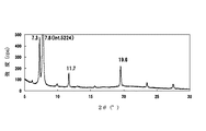
前記有機半導体層におけるCuKαX線回折のブラッグ角(2θ)が8.4°±0.2°、11.9°±0.2°、16.9°±0.2°にピークを有することを特徴とする電界効果型トランジスタを提供する。
The present invention is a field effect transistor having an organic semiconductor layer, wherein an organic semiconductor layer containing at least a porphyrin and a layer made of at least a polysiloxane compound are adhered and laminated ,
The polysiloxane compound is a compound obtained by heating methylsilsesquioxane,
The porphyrin is a tetrabenzoporphyrin copper complex,
The Bragg angle (2θ) of CuKα X-ray diffraction in the organic semiconductor layer has peaks at 8.4 ° ± 0.2 °, 11.9 ° ± 0.2 °, and 16.9 ° ± 0.2 °. A field effect transistor is provided.
本発明によれば、結晶性、配向性に優れ、電界効果移動度が大きい電界効果型トランジスタを提供することができる。
また、本発明によれば、上記の電界効果型トランジスタを簡便な方法で得ることができる電界効果型トランジスタの製造方法を提供することができる。
According to the present invention, a field effect transistor having excellent crystallinity and orientation and high field effect mobility can be provided.
In addition, according to the present invention, it is possible to provide a method for manufacturing a field effect transistor that can obtain the above-described field effect transistor by a simple method.
以下、本発明を詳細に説明する。
本実施の形態に係る電界効果型トランジスタは、有機半導体と、絶縁体と、導電体を少なくとも有する素子である。絶縁体は、電極である導電体を覆うための絶縁膜(層)である。有機半導体はそのような導電体(電極)が発生する刺激(電界)に対して応答する有機半導体層である。具体的には電界に対して電気的特性が変化する層である。更に具体的には導電率、つまり有機半導体層を流れる電流が電界の変化に応じて変化する層である。
Hereinafter, the present invention will be described in detail.
The field effect transistor according to this embodiment is an element having at least an organic semiconductor, an insulator, and a conductor. The insulator is an insulating film (layer) for covering a conductor as an electrode. An organic semiconductor is an organic semiconductor layer that responds to a stimulus (electric field) generated by such a conductor (electrode). Specifically, it is a layer whose electrical characteristics change with respect to an electric field. More specifically, it is a layer in which the conductivity, that is, the current flowing through the organic semiconductor layer changes in accordance with the change in the electric field.
図1(a)は本実施形態に係る電界効果型トランジスタを示す模式的な概略断面図である。8は基材、1はゲート電極、2はゲート絶縁層、4はソース電極、5はドレイン電極、6は有機半導体層、7は封止層である。この素子は、基材8の表面にゲート電極1が設けられ、その上にゲート絶縁層2が設けられ、絶縁層3の表面にソース電極4とドレイン電極5が間隔をおいて設けられている。そしてソース電極4とドレイン電極5の上とその離間領域である絶縁層2上に有機半導体層6が両電極4、5と接して設けられている。絶縁層2はゲート電極2を覆うように設けられている。さらに、有機半導体層6上を封止層7で覆われている。また、基材8と封止層7を入れ替えることもできる。
FIG. 1A is a schematic schematic cross-sectional view showing a field effect transistor according to this embodiment. 8 is a base material, 1 is a gate electrode, 2 is a gate insulating layer, 4 is a source electrode, 5 is a drain electrode, 6 is an organic semiconductor layer, and 7 is a sealing layer. In this element, a gate electrode 1 is provided on the surface of a substrate 8, a gate insulating layer 2 is provided thereon, and a source electrode 4 and a
本実施形態に係る電界効果型トランジスタは、ゲート電極1に電圧を印加すると、ゲート絶縁層2と有機半導体層6との界面に正または負の電荷が誘起される。さらにソース電極4とドレイン電極5の間に電圧を印加すると、電荷が両電極間を移動し、電流を得ることができる。それ故、ゲート電極1に電圧を印加した際に、ゲート絶縁層2と有機半導体層6との界面に均一に電荷が生じ、さらにソース電極4とドレイン電極5の間に電圧を印加した際に、障壁が少なく、効率良く電荷が移動することによって、高い電界効果移動度を示すことができる。
In the field effect transistor according to the present embodiment, when a voltage is applied to the gate electrode 1, positive or negative charges are induced at the interface between the gate insulating layer 2 and the organic semiconductor layer 6. Further, when a voltage is applied between the source electrode 4 and the
本発明者らは電荷が均一に発生し、かつ、発生した電荷が効率良く移動できる有機半導体層界面を形成するための方法を探すべく鋭意検討を重ねたところ、電荷が移動する界面(図1ではゲート絶縁層2と有機半導体層6の界面)を挟んで、特定の有機半導体材料と、結晶化を促進する層(結晶化促進層)とを積層することによって、その界面で連続的に均一で欠陥の少ない結晶が形成可能になり、高い電界効果移動度を示すことを見出すに至った。 The present inventors have intensively studied to find a method for forming an organic semiconductor layer interface in which charges are uniformly generated and the generated charges can efficiently move. Then, by sandwiching a specific organic semiconductor material and a layer for promoting crystallization (crystallization promoting layer) across the gate insulating layer 2 and the organic semiconductor layer 6), the interface is continuously uniform at the interface. Thus, a crystal with few defects can be formed, and it has been found that high field-effect mobility is exhibited.
本発明の電界効果型トランジスタは、有機半導体層を有する電界効果型トランジスタであって、好ましくは、少なくともポルフィリンを含有する有機半導体層と、少なくともポリシロキサン化合物からなる層が密着して積層されていることを特徴とする。ここで言う密着とは、有機半導体層とポリシロキサン化合物からなる層が他の層を介さずに接している状態を指す。 The field effect transistor of the present invention is a field effect transistor having an organic semiconductor layer, and preferably, an organic semiconductor layer containing at least a porphyrin and at least a layer made of a polysiloxane compound are closely adhered to each other. It is characterized by that. The adhesion mentioned here refers to a state in which the organic semiconductor layer and the layer made of the polysiloxane compound are in contact with each other without any other layer.
本発明において、ポリシロキサン化合物からなる層(以下A層とする)とポルフィリンを有する有機半導体層(以下B層とする)とが、素子内の一部又は全面において密着して積層されている電界効果型トランジスタは、高い電界効果移動度を示すため好ましい。また後述するが、ポルフィリンの前駆体を可溶性にすれば、A層、B層ともに塗布工程を用いて作製することができるために簡便なプロセスで素子を作製することが可能である。 In the present invention, an electric field in which a layer made of a polysiloxane compound (hereinafter referred to as A layer) and a porphyrin-containing organic semiconductor layer (hereinafter referred to as B layer) are laminated in close contact with each other in part or on the entire surface of the device. An effect transistor is preferable because it exhibits high field-effect mobility. As will be described later, if the porphyrin precursor is made soluble, both the A layer and the B layer can be prepared using a coating process, and thus the device can be manufactured by a simple process.
さらに、後述するように、A層に代えて、他の結晶化促進機能を有する結晶化促進層を用いることが可能であるし、B層に代えて、当該結晶化促進層によって結晶化が促進されるような有機半導体層を用いることが可能である。 Furthermore, as will be described later, it is possible to use another crystallization promoting layer having a crystallization promoting function instead of the A layer, and crystallization is promoted by the crystallization promoting layer instead of the B layer. It is possible to use such an organic semiconductor layer.
なお、本発明において、結晶化促進層が形成される下地の構造体(一般的には、基材、ゲート電極、ゲート絶縁層からなる構造体。ただし、ゲート絶縁層は省略可能な場合もあるし、積層順によっては、基材のみの場合もある。その他の層が形成されている場合もある。)を基体と呼ぶ場合もある。また、本発明において、結晶化促進機能とは、結晶粒の安定化(移動や回転を伴なう場合もある)及び/又は結晶粒同士の接合を促進する機能を言い、結晶化促進層とは、結晶粒の安定化(移動や回転を伴なう場合もある)及び/又は結晶粒同士の接合を促進する層である。 In the present invention, the underlying structure on which the crystallization promoting layer is formed (generally a structure comprising a base material, a gate electrode, and a gate insulating layer. However, the gate insulating layer may be omitted in some cases. Depending on the order of lamination, the substrate may be used alone, or other layers may be formed). In the present invention, the crystallization promoting function refers to a function of promoting stabilization of crystal grains (sometimes accompanied by movement or rotation) and / or joining of crystal grains, Is a layer that promotes the stabilization of crystal grains (sometimes accompanied by movement and rotation) and / or the bonding of crystal grains.
以下では、A層の上にB層が形成されるが、本発明はこれらに限定されない。もっとも、B層形成時にA層による影響力を与えるという観点からは、A層の上にB層を形成することが好ましい。 In the following, the B layer is formed on the A layer, but the present invention is not limited thereto. However, from the viewpoint of giving influence by the A layer when forming the B layer, it is preferable to form the B layer on the A layer.
本発明のポリシロキサン化合物は、シロキサン構造(−Si−O−)と有機シラン構造を有する重合体であり、その他の有機高分子や無機高分子との共重合体であっても構わない。他の高分子との重合体の場合、シロキサン構造と有機シラン構造を主鎖中に導入されていても、側鎖にグラフトされていても構わない。シロキサン構造(−Si−O−)と有機シラン構造との組み合わせの効果によって、B層の有機半導体層は結晶化の過程でA層からの束縛を受け難い為、結晶化が促進する。 The polysiloxane compound of the present invention is a polymer having a siloxane structure (—Si—O—) and an organic silane structure, and may be a copolymer with other organic polymer or inorganic polymer. In the case of a polymer with another polymer, the siloxane structure and the organosilane structure may be introduced into the main chain or may be grafted to the side chain. Due to the effect of the combination of the siloxane structure (—Si—O—) and the organic silane structure, the organic semiconductor layer of the B layer is less likely to be bound by the A layer during the crystallization process, and thus crystallization is promoted.
本発明のポリシロキサン化合物は直鎖状もしくは環状でも構わないが、高次に架橋もしくは分岐した構造を持つことがより好ましい。ここで述べる、高次に架橋もしくは分岐した構造とは、網状、梯子状、籠状、星状、樹状構造も含む。また、架橋もしくは分岐した構造は、必ずしもシロキサン構造を介して形成されなければならないわけではなく、ビニル基、アクリロイル基、エポキシ基、シンナモイル基などの有機基同士が架橋した構造や、3官能以上の有機基を介して分岐した構造を含んでも構わない。 The polysiloxane compound of the present invention may be linear or cyclic, but more preferably has a high-order crosslinked or branched structure. The higher-order bridged or branched structure described here includes a net-like, ladder-like, cage-like, star-like, and dendritic structure. In addition, the crosslinked or branched structure does not necessarily have to be formed via a siloxane structure, and a structure in which organic groups such as vinyl group, acryloyl group, epoxy group, cinnamoyl group are crosslinked with each other, or a trifunctional or more functional group. A structure branched via an organic group may be included.
本発明のポリシロキサン化合物の層は、高次に架橋もしくは分岐した構造を持つことによって、基材表面の活性基にオクチルトリクロロシランやヘキサメチルジシラザンなどを反応させてできる単分子層とは異なり、基体表面の状態や形状には依存されず、広い面積に非晶質な層を形成できる。そのため、少なくともチャネルを形成する領域以上の広い範囲において、A層とB層の界面は均一となり、前述したシロキサン構造と有機シラン構造との組み合わせの効果とも相まって、連続的に均一で欠陥の少ない結晶が形成される。 The polysiloxane compound layer of the present invention is different from a monomolecular layer formed by reacting octyltrichlorosilane or hexamethyldisilazane with an active group on the substrate surface by having a high-order crosslinked or branched structure. The amorphous layer can be formed over a wide area regardless of the state and shape of the substrate surface. For this reason, the interface between the A layer and the B layer is uniform at least in a wide range beyond the region where the channel is formed, and is combined with the above-described effect of the combination of the siloxane structure and the organosilane structure, so that the crystal is continuously uniform and has few defects. Is formed.
本発明のA層に用いられるポリシロキサン化合物は、例えば、下記一般式(1)に示される構造を有し、主鎖がシロキサンユニット、側鎖が水素原子又は炭素原子等の有機基を有する置換基である。 The polysiloxane compound used in the A layer of the present invention has, for example, a structure represented by the following general formula (1), a main chain having a siloxane unit, and a side chain having an organic group such as a hydrogen atom or a carbon atom. It is a group.

式中、R1 〜R4 は置換または非置換の炭素原子数1〜5のアルキル基、アルケニル基、置換または非置換のフェニル基またはシロキサンユニットのいずれかである。R1 〜R4 の各々は同じでも異なっていてもよい。nは1以上の整数である。 In the formula, each of R 1 to R 4 is a substituted or unsubstituted alkyl group having 1 to 5 carbon atoms, an alkenyl group, a substituted or unsubstituted phenyl group, or a siloxane unit. Each of R 1 to R 4 may be the same or different. n is an integer of 1 or more.
置換基R1 〜R4 は、下記に示すようなシロキサンユニットでも良い。 The substituents R 1 to R 4 may be siloxane units as shown below.
(式中、Rは置換または非置換の炭素原子数1〜5のアルキル基、アルケニル基、または置換または非置換のフェニル基または上記に表されているシロキサンユニットのいずれかであり、各々同じ官能基であっても違う官能基であっても良い。) (Wherein R is a substituted or unsubstituted alkyl group having 1 to 5 carbon atoms, an alkenyl group, a substituted or unsubstituted phenyl group, or a siloxane unit represented above, each having the same functionality. Or a different functional group.)
一般式(1)中の置換基の種類によってポリシロキサンの形状には直鎖状、環状、網状、梯子状、籠状構造等が存在するが、本発明に用いるポリシロキサンはそのいずれでも構わない。 Depending on the type of the substituent in the general formula (1), the polysiloxane may have a linear, cyclic, network, ladder, or cage structure, and any of the polysiloxanes used in the present invention may be used. .
本発明において、A層に用いられるポリシロキサン化合物として特に好ましいのは、少なくとも下記の一般式(2)に示すような特定のシルセスキオキサン骨格および/または下記の一般式(6)に示すような特定のオルガノシロキサン骨格を有するポリシロキサン化合物である。 In the present invention, particularly preferred as the polysiloxane compound used in the A layer is at least a specific silsesquioxane skeleton as shown in the following general formula (2) and / or as shown in the following general formula (6). It is a polysiloxane compound having a specific organosiloxane skeleton.
(式中、R7 〜R10は置換または非置換の炭素原子数1〜5のアルキル基、アルケニル基または置換または非置換のフェニル基のいずれかである。R7 〜R10の各々は同じでも異なっていてもよい。mおよびnは0以上の整数であり、mとnの和は1以上の整数である。共重合の形態はランダム共重合であってもブロック共重合であっても良い。) (Wherein R 7 to R 10 are any of substituted or unsubstituted alkyl groups having 1 to 5 carbon atoms, alkenyl groups, or substituted or unsubstituted phenyl groups. Each of R 7 to R 10 is the same. However, m and n are integers greater than or equal to 0, and the sum of m and n is an integer greater than or equal to 1. The form of copolymerization may be random copolymerization or block copolymerization. good.)
(式中、R21〜R24は置換または非置換の炭素原子数1〜5のアルキル基、アルケニル基、または置換または非置換のフェニル基のいずれかである。R21〜R24の各々は同じでも異なっていてもよい。rおよびpは0以上の整数であり、rとpの和は1以上の整数である。共重合の形態はランダム共重合であってもブロック共重合であっても良い。)
また、一般式(2)で示されるシルセスキオキサン骨格と一般式(6)で示されるオルガノシロキサン骨格とはいずれか一方を含んでも、両方を含んでも構わない。
(In the formula, each of R 21 to R 24 is a substituted or unsubstituted alkyl group having 1 to 5 carbon atoms, an alkenyl group, or a substituted or unsubstituted phenyl group. Each of R 21 to R 24 is R and p are integers greater than or equal to 0, and the sum of r and p is an integer greater than or equal to 1. The form of copolymerization is random copolymerization or block copolymerization, Is also good.)
The silsesquioxane skeleton represented by the general formula (2) and the organosiloxane skeleton represented by the general formula (6) may include either one or both.
また、上記シルセスキオキサン骨格およびオルガノシロキサン骨格の側鎖に相当する炭素原子を有する置換基R7 〜R10およびR21〜R24は置換または非置換の炭素原子数1〜5個のアルキル基、アルケニル基もしくは置換または非置換のフェニル基であり、箇所によって同じ官能基であっても違う官能基であっても良い。例えば、メチル基、エチル基のような非置換アルキル基/非置換のフェニル基/ジメチルフェニル基やナフチル基といった置換フェニル基などが挙げられる。また、置換基R7 〜R10には炭素原子、水素原子の他に酸素原子や窒素原子や金属原子など各種の原子が含まれていて良い。 The substituents R 7 to R 10 and R 21 to R 24 having carbon atoms corresponding to the side chains of the silsesquioxane skeleton and organosiloxane skeleton are substituted or unsubstituted alkyl having 1 to 5 carbon atoms. A group, an alkenyl group, or a substituted or unsubstituted phenyl group, which may be the same functional group or different functional groups depending on the position. For example, an unsubstituted alkyl group such as a methyl group or an ethyl group / an unsubstituted phenyl group / a substituted phenyl group such as a dimethylphenyl group or a naphthyl group. Further, the substituents R 7 to R 10 may contain various atoms such as oxygen atom, nitrogen atom and metal atom in addition to carbon atom and hydrogen atom.
以下、本発明に用いられる化合物のシルセスキオキサン骨格について説明する。一般式(2)では、置換基R7 、R8 を有するシルセスキオキサンユニット(以後、第一ユニット)がm個繰り返したものと、置換基R9 、R10を有するシルセスキオキサンユニット(以後、第二ユニット)がn個繰り返したものが接続した構造式が示されている(mおよびnは0以上の整数であり、m+nは1以上の整数である)が、これは第一ユニットの繰り返しと、第二ユニットの繰り返しが分離していることを意味するのではない。両ユニットは、分離して接続していてもランダムに入り交じって接続していても良い。 Hereinafter, the silsesquioxane skeleton of the compound used in the present invention will be described. In the general formula (2), m silsesquioxane units having substituents R 7 and R 8 (hereinafter referred to as first unit) are repeated, and silsesquioxane units having substituents R 9 and R 10. A structural formula is shown in which n (second unit) repeats are connected (m and n are integers greater than or equal to 0, and m + n is an integer greater than or equal to 1). It does not mean that the repetition of the unit and the repetition of the second unit are separated. Both units may be connected separately or may be connected randomly.
一般式(6)では、置換基R21、R22を有するジオルガノシロキサンユニット(以後、第一ユニット)がr個繰り返したものと、置換基R23、R24を有するジオルガノシロキサンユニット(以後、第二ユニット)がp個繰り返したものが接続した構造式が示されている(rおよびpは0以上の整数であり、r+pは1以上の整数である)が、これは第一ユニットの繰り返しと、第二ユニットの繰り返しが分離していることを意味するのではない。両ユニットは、分離して接続していてもランダムに入り交じって接続していても良い。 In the general formula (6), a diorganosiloxane unit having substituents R 21 and R 22 (hereinafter referred to as the first unit) and a diorganosiloxane unit having substituents R 23 and R 24 (hereinafter referred to as the first unit) are repeated. , The second unit) is a p-linked structure (r and p are integers greater than or equal to 0, and r + p is an integer greater than or equal to 1). It does not mean that the repetition and the repetition of the second unit are separated. Both units may be connected separately or may be connected randomly.
一般式(2)や一般式(6)に示すようなシルセスキオキサン骨格および/またはオルガノシロキサン骨格を有するポリシロキサン化合物を主体として含有する本発明におけるA層を形成するためには、例えば、下記の一般式(4)および一般式(5)もしくはいずれか一方に示すポリオルガノシルセスキオキサン化合物および/または下記の一般式(7)および一般式(8)もしくはいずれか一方に示すポリオルガノシロキサン化合物を含む溶液を基板上に塗布して、加熱乾燥させる方法と、ケイ素モノマーを加水分解して得られるゾルを基板上に塗布して、加熱乾燥させる方法とがある。 In order to form the layer A in the present invention mainly containing a polysiloxane compound having a silsesquioxane skeleton and / or an organosiloxane skeleton as shown in the general formula (2) or the general formula (6), for example, A polyorganosilsesquioxane compound represented by the following general formula (4) and / or general formula (5) and / or a polyorgano represented by the following general formula (7) and / or general formula (8) There are a method in which a solution containing a siloxane compound is applied on a substrate and heat-dried, and a method in which a sol obtained by hydrolyzing a silicon monomer is applied on a substrate and heat-dried.
前者の一般式(4)および一般式(5)もしくはいずれか一方に示すポリオルガノシルセスキオキサン化合物および/または下記の一般式(7)および一般式(8)もしくはいずれか一方に示すポリオルガノシロキサン化合物の塗膜を加熱乾燥させる方法では、加熱により化合物の末端同士が脱水もしくは脱アルコール反応により縮合することで、ポリオルガノシルセスキオキサン化合物はラダー状に接続され、一方、ポリオルガノシロキサン化合物は高分子量化して、緻密化する。ただしこの時、乾燥温度は有機物が完全に消失するほど高くないので原料化合物は完全なシリカ構造にまでにはならずに大部分の置換基が残存している一般式(2)や(6)に示すようなシルセスキオキサン骨格もしくはオルガノシロキサン骨格となる。 The polyorganosilsesquioxane compound represented by the general formula (4) and / or the general formula (5) and / or the polyorgano represented by the following general formula (7) and the general formula (8) or any one of the following: In the method of heating and drying the coating film of the siloxane compound, the polyorganosilsesquioxane compound is connected in a ladder form by condensing the ends of the compound by heating through dehydration or dealcoholization reaction, while the polyorganosiloxane compound Increases in molecular weight and densifies. However, at this time, the drying temperature is not so high that the organic matter is completely disappeared. A silsesquioxane skeleton or an organosiloxane skeleton as shown in FIG.
一般式(4)および一般式(5)に示すポリオルガノシルセスキオキサン化合物および一般式(7)および一般式(8)に示すポリオルガノシロキサン化合物は市販されたものを用いることができるが、一般的にポリオルガノシルセスキオキサン化合物やポリオルガノシロキサン化合物はそれぞれ下記反応式(11)および反応式(12)で示される反応によって合成される。 Commercially available polyorganosilsesquioxane compounds represented by general formula (4) and general formula (5) and polyorganosiloxane compounds represented by general formula (7) and general formula (8) can be used. Generally, a polyorganosilsesquioxane compound and a polyorganosiloxane compound are synthesized by the reactions shown in the following reaction formula (11) and reaction formula (12), respectively.
上記反応式(11)および(12)について説明する。有機基R’を有する3官能性有機ケイ素モノマーおよび/または2官能性有機ケイ素モノマーをアルコールなどの溶媒中、加水分解してシラノール化合物を生成する。上記式中に示すケイ素モノマーはアルコキシドであり、加水分解によってR’’OHが脱離するが、他にもクロライドをケイ素モノマーとして用いることができる。ただし、この場合の脱離成分として塩化水素が発生する。加水分解によって得られたシラノール化合物は、さらに加熱などによって脱水縮合し、ポリオルガノシルセスキオキサン化合物およびポリオルガノシロキサン化合物が生成する。溶媒や触媒などを除去することで、ポリオルガノシルセスキオキサン化合物およびポリオルガノシロキサン化合物が固体として単離される。得られる化合物の構造や分子量、末端基の種類などは反応の際の触媒、溶媒、pH、濃度などによって変化させることができる。 The reaction formulas (11) and (12) will be described. A trifunctional organosilicon monomer and / or a bifunctional organosilicon monomer having an organic group R ′ is hydrolyzed in a solvent such as alcohol to produce a silanol compound. The silicon monomer shown in the above formula is an alkoxide, and R ″ OH is eliminated by hydrolysis, but chloride can also be used as the silicon monomer. However, hydrogen chloride is generated as a desorbing component in this case. The silanol compound obtained by hydrolysis is further subjected to dehydration condensation by heating or the like to produce a polyorganosilsesquioxane compound and a polyorganosiloxane compound. By removing the solvent and the catalyst, the polyorganosilsesquioxane compound and the polyorganosiloxane compound are isolated as solids. The structure, molecular weight, type of terminal group, and the like of the resulting compound can be changed depending on the catalyst, solvent, pH, concentration, etc. during the reaction.
(式中、R7 、R8 は置換または非置換の炭素原子数1〜5のアルキル基、アルケニル基または置換または非置換のフェニル基のいずれかであり、R7 とR8 は同じ官能基であっても良い。R13〜R16は炭素原子数1〜4のアルキル基または水素原子であり、zは1以上の整数である。) (Wherein R 7 and R 8 are either substituted or unsubstituted alkyl groups having 1 to 5 carbon atoms, alkenyl groups or substituted or unsubstituted phenyl groups, and R 7 and R 8 are the same functional group. R 13 to R 16 are an alkyl group having 1 to 4 carbon atoms or a hydrogen atom, and z is an integer of 1 or more.)
(式中、R9 、R10は置換または非置換の炭素原子数1〜5のアルキル基、アルケニル基または置換または非置換のフェニル基のいずれかであり、R9 とR10は同じ官能基であっても良い。R17〜R20は炭素原子数1〜4のアルキル基または水素原子であり、yは1以上の整数である。) (In the formula, R 9 and R 10 are each a substituted or unsubstituted alkyl group having 1 to 5 carbon atoms, an alkenyl group, or a substituted or unsubstituted phenyl group, and R 9 and R 10 are the same functional group. R 17 to R 20 are each an alkyl group having 1 to 4 carbon atoms or a hydrogen atom, and y is an integer of 1 or more.)
(式中、R25、R26は置換または非置換の炭素原子数1〜5のアルキル基、アルケニル基、または置換または非置換のフェニル基いずれかであり、R25とR26は同じ官能基であっても良い。R27、R28は炭素原子数1〜4のアルキル基または水素原子であり、qは1以上の整数である。) (In the formula, R 25 and R 26 are either substituted or unsubstituted alkyl groups having 1 to 5 carbon atoms, alkenyl groups, or substituted or unsubstituted phenyl groups, and R 25 and R 26 are the same functional group. R 27 and R 28 are each an alkyl group having 1 to 4 carbon atoms or a hydrogen atom, and q is an integer of 1 or more.)
(式中、R29、R30は置換または非置換の炭素原子数1〜5のアルキル基、アルケニル基、または置換または非置換のフェニル基のいずれかであり、R29とR30は同じ官能基であっても良い。R31、R32は炭素原子数1〜4のアルキル基または水素原子であり、sは1以上の整数である。)
また、乾燥工程に際してオリゴマーであるシルセスキオキサン化合物が互いに架橋しあう反応を補助する目的で、塗布溶液にはギ酸などの酸を少量添加してもよい。
(Wherein R 29 and R 30 are either a substituted or unsubstituted alkyl group having 1 to 5 carbon atoms, an alkenyl group, or a substituted or unsubstituted phenyl group, and R 29 and R 30 have the same functionality. R 31 and R 32 may be an alkyl group having 1 to 4 carbon atoms or a hydrogen atom, and s is an integer of 1 or more.)
In addition, a small amount of acid such as formic acid may be added to the coating solution for the purpose of assisting the reaction in which the oligomeric silsesquioxane compounds cross-link each other during the drying step.
酸の添加量は特に限定されるものではないが、ギ酸の場合は、塗布溶液に含まれるポリオルガノシルセスキオキサン化合物の固形分重量に対して1重量%から30重量%の範囲で添加すると架橋反応が促進される。添加量が1重量%より少ないと架橋反応の促進効果が十分でなくなり、逆に添加量が30重量%より多いと乾燥後の膜化を阻害するおそれがある。 The amount of acid to be added is not particularly limited, but in the case of formic acid, it is added in the range of 1 to 30% by weight with respect to the solid weight of the polyorganosilsesquioxane compound contained in the coating solution. Cross-linking reaction is promoted. If the addition amount is less than 1% by weight, the effect of promoting the crosslinking reaction is not sufficient, and conversely if the addition amount is more than 30% by weight, film formation after drying may be hindered.
一方、ケイ素モノマーを加水分解して得られるゾルを基板上に塗布して、加熱乾燥させる方法について説明する。前記反応式(11)および反応式(12)に示した3官能ケイ素モノマーおよび/または2官能ケイ素モノマーを溶媒中で、水および触媒共存させて室温もしくは加熱しながら攪拌すると、反応式(11)および反応式(12)同様の加水分解、脱水縮合反応を経由してゾルを調製する。得られたゾルの塗膜を加熱すると、シラノールや未反応のアルコキシド同士が脱水もしくは脱アルコール反応により縮合し、緻密な一般式(2)や(6)に示すようなシルセスキオキサン骨格もしくはオルガノシロキサン骨格を形成する。 On the other hand, a method of applying a sol obtained by hydrolyzing a silicon monomer on a substrate and drying by heating will be described. When the trifunctional silicon monomer and / or the bifunctional silicon monomer shown in the reaction formula (11) and the reaction formula (12) are stirred in a solvent in the presence of water and a catalyst at room temperature or with heating, the reaction formula (11) And a sol is prepared through hydrolysis and dehydration condensation reaction similar to the reaction formula (12). When the obtained sol coating is heated, silanols and unreacted alkoxides are condensed by dehydration or dealcoholization reaction, resulting in a dense silsesquioxane skeleton or organo group as shown in general formulas (2) and (6). A siloxane skeleton is formed.
ゾルを調製するために使用できる代表的なケイ素モノマーとしては、メチルトリメトキシシラン、メチルトリエトキシシラン、エチルトリメトキシシラン、エチルトリエトキシシラン、ブチルトリメトキシシラン、ビニルトリメトキシシラン、3−アミノプロピルトリエトキシシランやフェニルトリメトキシシランなどの3官能ケイ素モノマー、ジメチルジメトキシシランやジフェニルジメトキシシランなどの2官能ケイ素モノマーが挙げられる。 Typical silicon monomers that can be used to prepare the sol include methyltrimethoxysilane, methyltriethoxysilane, ethyltrimethoxysilane, ethyltriethoxysilane, butyltrimethoxysilane, vinyltrimethoxysilane, 3-aminopropyl Examples thereof include trifunctional silicon monomers such as triethoxysilane and phenyltrimethoxysilane, and bifunctional silicon monomers such as dimethyldimethoxysilane and diphenyldimethoxysilane.
ゾルの調製には、モノマーの加水分解を促進するために、水と触媒を加えることができる。水の添加量は前記反応式(11)または反応式(12)中のモノマーのOR’’基に対し0.1〜20当量である。一方、触媒は酸または塩基触媒を用いることができる。酸触媒としては塩酸、硝酸、p−トルエンスルホン酸、トリフルオロメタンスルホン酸、酢酸、ギ酸、トリフルオロ酢酸、アルキル燐酸などを使用できるが、腐食性が低く、塗膜の加熱乾燥時に揮発して膜中に残存しないなどの点からギ酸がより好ましい。塩基触媒としては水酸化ナトリウム、水酸化カリウム、水酸化テトラメチルアンモニウムなどを使用できるが、ナトリウムなどのアルカリ金属の残存は素子としての電気特性を悪化させる原因になることから、水酸化テトラメチルアンモニウムが好ましい。触媒の添加量は、溶液に含まれるケイ素モノマーの固形分重量に対して1重量%から30重量%の範囲で添加すると加水分解反応が促進される。添加量が1重量%より少ないと架橋反応の促進効果が十分でなくなり、逆に添加量が30重量%より多いと乾燥後の膜性を悪化するおそれがある。 To prepare the sol, water and a catalyst can be added to promote hydrolysis of the monomer. The amount of water added is 0.1 to 20 equivalents relative to the OR ″ group of the monomer in the reaction formula (11) or the reaction formula (12). On the other hand, an acid or base catalyst can be used as the catalyst. Hydrochloric acid, nitric acid, p-toluenesulfonic acid, trifluoromethanesulfonic acid, acetic acid, formic acid, trifluoroacetic acid, alkyl phosphoric acid, etc. can be used as the acid catalyst, but it is low corrosive and volatilizes when the coating is heated and dried. Formic acid is more preferable because it does not remain in it. Sodium hydroxide, potassium hydroxide, tetramethylammonium hydroxide, etc. can be used as the base catalyst, but the remaining of alkali metals such as sodium causes deterioration of the electrical characteristics of the device, so tetramethylammonium hydroxide Is preferred. When the catalyst is added in an amount of 1 to 30% by weight based on the solid content weight of the silicon monomer contained in the solution, the hydrolysis reaction is promoted. If the addition amount is less than 1% by weight, the crosslinking reaction is not sufficiently promoted. Conversely, if the addition amount is more than 30% by weight, the film properties after drying may be deteriorated.
また、一般式(4)および一般式(5)に示すポリオルガノシルセスキオキサン化合物および一般式(7)および一般式(8)に示すポリオルガノシロキサン化合物と前記反応式(11)または反応式(12)中のケイ素モノマーを混合して用いることもできる。この場合、ゾルの調製と同様、水や触媒を加えることができる。水の添加量はモノマーのOR’’基に対し0.1〜20当量であり、触媒の添加量は、ポリオルガノシルセスキオキサン化合物および/またはポリオルガノシロキサン化合物とケイ素モノマーを加えた固形分重量に対して1重量%から30重量%であることが好ましい。 Further, the polyorganosilsesquioxane compound represented by the general formula (4) and the general formula (5) and the polyorganosiloxane compound represented by the general formula (7) and the general formula (8) and the above reaction formula (11) or the reaction formula The silicon monomer in (12) can also be mixed and used. In this case, water and a catalyst can be added similarly to preparation of sol. The amount of water added is 0.1 to 20 equivalents relative to the OR ″ group of the monomer, and the amount of catalyst added is the solid content of the polyorganosilsesquioxane compound and / or polyorganosiloxane compound and the silicon monomer. The content is preferably 1% by weight to 30% by weight based on the weight.
さらに、塗布性や加熱後の対溶剤性を高めるために、テトラメトキシシランやテトラエトキシシランなどの4官能ケイ素モノマーを併用することができる。
好ましい加熱処理温度は140℃以上、さらに好ましくは150〜230℃である。140℃未満で加熱すると加水分解反応が不十分となるおそれがある。
Furthermore, tetrafunctional silicon monomers such as tetramethoxysilane and tetraethoxysilane can be used in combination in order to improve the coating property and solvent resistance after heating.
A preferable heat treatment temperature is 140 ° C. or higher, and more preferably 150 to 230 ° C. If it is heated below 140 ° C., the hydrolysis reaction may be insufficient.
架橋反応、溶剤除去の過程において、系内にはその温度領域で蒸発、揮発、焼失しない安定剤は溶液系から極力除去する。
塗布溶液の溶媒にはアルコール類やエステル類など任意のものを使用できる。基板への濡れ性などを考慮して溶媒を選択すればよい。
In the process of cross-linking reaction and solvent removal, the stabilizer that does not evaporate, volatilize or burn out in the temperature region is removed from the solution system as much as possible.
Arbitrary things, such as alcohol and ester, can be used for the solvent of a coating solution. A solvent may be selected in consideration of wettability to the substrate.
A層の原料溶液の塗布方法は特に限定されるものではなく、慣用のコーティング方法、例えばスピンコーティング法、キャスト法、スプレー塗布法、ドクターブレード法、ダイコーティング法、ディッピング法、印刷法、インクジェット法、滴下法等により塗布する。これらの方法のうち、塗布量を制御して所望の膜厚の成膜ができるという点で好ましい方法はスピンコーティング法、ディッピング法、スプレー塗布法、インクジェット法である。また、得られた膜の絶縁性を保つためには塗布溶液に極力ゴミなどを混入させないことが重要であり、事前に原料溶液をメンブランフィルタで濾過することが望ましい。 The coating method of the raw material solution for the A layer is not particularly limited, and a conventional coating method such as a spin coating method, a casting method, a spray coating method, a doctor blade method, a die coating method, a dipping method, a printing method, or an ink jet method. Apply by a dropping method or the like. Among these methods, a preferable method is a spin coating method, a dipping method, a spray coating method, and an ink jet method in that a film thickness of a desired thickness can be formed by controlling the coating amount. Further, in order to maintain the insulating properties of the obtained film, it is important that dust and the like are not mixed in the coating solution as much as possible, and it is desirable to filter the raw material solution with a membrane filter in advance.
A層の膜厚は10nm以上、好ましくは15〜500nmになるように液濃度を調整することが好ましい。10nm未満になると、均一な膜が得られにくくなるからである。
A層を塗布する前に基板をアルカリ液による超音波処理やUV照射等で濡れ性向上のための表面改質を行ってもよい。
It is preferable to adjust the liquid concentration so that the thickness of the A layer is 10 nm or more, preferably 15 to 500 nm. This is because when the thickness is less than 10 nm, it is difficult to obtain a uniform film.
Before applying the A layer, the substrate may be subjected to surface modification for improving wettability by ultrasonic treatment with an alkaline solution or UV irradiation.
次に、本発明のB層の好ましい態様について説明する。B層は、好ましくは少なくとも下記の一般式(3)で表されるポルフィリン化合物を含有する。 Next, the preferable aspect of B layer of this invention is demonstrated. The B layer preferably contains at least a porphyrin compound represented by the following general formula (3).
式中、R11はそれぞれ水素原子、ハロゲン原子、水酸基、または炭素原子数1以上12以下のアルキル基、オキシアルキル基、チオアルキル基、アルキルエステル基より選ばれる少なくとも1種を示し、R11は同じ又は異なっていてよい。また、隣接するR11同士が、置換基を有していてもよい芳香環を形成していてもよい。また、隣接するR11同士が形成した芳香環を通して、置換基を有していてもよいポルフィリン環と連結していてもよい。R12は水素原子または置換基を有していてもよいアリール基より選ばれる少なくとも1種を示す。R12は同じ又は異なっていてよい。またXは水素原子または金属原子を示す。Xの一例として、H、Cu、Zn、Ni、Co、Mg、Fe等の各種金属や、AlCl、TiO、FeCl、SiCl2等の原子団などである。Xは特に限定されないが、水素原子または銅原子が特に好ましい。芳香環としては例えば、ベンゼン環、ナフタレン環、アントラセン環等が挙げられる。 In the formula, R 11 represents at least one selected from a hydrogen atom, a halogen atom, a hydroxyl group, or an alkyl group having 1 to 12 carbon atoms, an oxyalkyl group, a thioalkyl group, and an alkyl ester group, and R 11 is the same. Or it may be different. Further, adjacent R 11 may form an aromatic ring which may have a substituent. Further, through the aromatic ring between R 11 adjacent is formed, it may be linked with good porphyrin ring which may have a substituent. R 12 represents at least one selected from a hydrogen atom or an aryl group which may have a substituent. R 12 may be the same or different. X represents a hydrogen atom or a metal atom. Examples of X include various metals such as H, Cu, Zn, Ni, Co, Mg, and Fe, and atomic groups such as AlCl, TiO, FeCl, and SiCl 2 . X is not particularly limited, but is particularly preferably a hydrogen atom or a copper atom. Examples of the aromatic ring include a benzene ring, a naphthalene ring, and an anthracene ring.
これらポルフィリン化合物は、A層が形成されている基板上に、真空蒸着法、分散塗布法等の一般的な手法で製膜することができる。
以下にポルフィリン化合物の一例を示す。無置換、無金属体の構造を主体に示しているが、置換基、中心金属、中心原子団は限定されない。もちろん本発明の化合物はこれらに限定されない。
These porphyrin compounds can be formed on a substrate on which the A layer is formed by a general method such as a vacuum deposition method or a dispersion coating method.
An example of a porphyrin compound is shown below. Although the structure of an unsubstituted and metal-free body is mainly shown, the substituent, the central metal, and the central atomic group are not limited. Of course, the compound of this invention is not limited to these.
先に述べたように、前記一般式(3)で表されるポルフィリン化合物の少なくとも1組の隣接するR11同士が、芳香環を形成していることが好ましいが、この芳香環がビシクロ[2.2.2]オクタジエン骨格構造を有する前駆体(以下ビシクロ体)の溶剤塗布により得られる塗膜の加熱により得られるのであれば、ポルフィリン化合物の結晶化を促進するためさらに好ましい。なお、加熱に代えて、光照射などの他のエネルギー付加手段を用いることも可能である。より一般的に言えば、逆ディールスアルダー反応(レトロディールスアルダー反応)を用いることが、塗布プロセスの使用を容易にするという点で好ましい。 As described above, it is preferable that at least one pair of adjacent R 11 of the porphyrin compound represented by the general formula (3) forms an aromatic ring, and this aromatic ring is bicyclo [2 2.2.2] If it is obtained by heating a coating film obtained by solvent coating of a precursor having an octadiene skeleton structure (hereinafter referred to as bicyclo form), it is more preferable in order to promote crystallization of the porphyrin compound. In addition, it is also possible to use other energy addition means, such as light irradiation, instead of heating. More generally speaking, it is preferable to use a reverse Diels-Alder reaction (retro Diels-Alder reaction) in terms of facilitating use of the coating process.
ビシクロ体を前駆体に用いたときのB層の作製法としては、ビシクロ体を有機溶媒に溶解させてから、A層が形成されている基材に塗布し、その後に加熱することでポルフィリン化合物の結晶化膜を得る方法が好ましい。 As a method for producing the B layer when the bicyclo body is used as a precursor, the bicyclo body is dissolved in an organic solvent, and then applied to the base material on which the A layer is formed, and then heated to obtain a porphyrin compound. A method for obtaining a crystallized film is preferable.
A層とB層は少なくとも一部で密着していれば良く、A層とB層の間には一部電極などの他の素子構成要素が存在してもよい。
B層を塗布する前に必要に応じてA層の表面を一般的な手法を用いて改質を行ってもよい。
It is sufficient that the A layer and the B layer are in close contact with each other, and another element component such as a partial electrode may exist between the A layer and the B layer.
Before applying the B layer, the surface of the A layer may be modified using a general method as necessary.
ビシクロ体を溶解するために用いられる有機溶媒はビシクロ体が反応したり、析出しなければ特に限定されない。また、2種以上の有機溶媒を混合して用いてもよい。塗膜表面の平滑性や膜厚の均一性を考慮に入れるとハロゲン溶媒を使用することが好ましい。ハロゲン溶媒の例としては、クロロホルム、塩化メチレン、ジクロロエタン、クロロベンゼン、ジクロロベンゼン、トリクロロベンゼン、1,2−ジクロロエチレンなどが挙げられる。溶液の濃度は所望の膜厚によって任意に調節されるが、好ましくは0.01〜5重量%である。 The organic solvent used for dissolving the bicyclo form is not particularly limited as long as the bicyclo form does not react or precipitate. Two or more organic solvents may be mixed and used. In consideration of the smoothness of the coating film surface and the uniformity of the film thickness, it is preferable to use a halogen solvent. Examples of the halogen solvent include chloroform, methylene chloride, dichloroethane, chlorobenzene, dichlorobenzene, trichlorobenzene, 1,2-dichloroethylene, and the like. The concentration of the solution is arbitrarily adjusted depending on the desired film thickness, but is preferably 0.01 to 5% by weight.
ビシクロ体を用いたときのB層の塗布方法としてはA層と同様に特に限定されるものではなく、慣用のコーティング方法、例えばスピンコーティング法、キャスト法、スプレー塗布法、ドクターブレード法、ダイコーティング法、ディッピング法、印刷法、インクジェット法、滴下法等により塗布する。これらの方法のうち、塗布量を制御して所望の膜厚の成膜ができるという点で好ましい方法はスピンコーティング法、ディッピング法、スプレー塗布法、インクジェット法である。 The application method of the B layer when using a bicyclo compound is not particularly limited as in the case of the A layer. Conventional coating methods such as a spin coating method, a casting method, a spray coating method, a doctor blade method, and a die coating are used. It is applied by the method, dipping method, printing method, ink jet method, dropping method or the like. Among these methods, a preferable method is a spin coating method, a dipping method, a spray coating method, and an ink jet method in that a film thickness of a desired thickness can be formed by controlling the coating amount.
また、半導体層中に極力ゴミなどを混入させないために事前にメンブランフィルタで濾過することが望ましい。なぜならば、不溶分や外部からのゴミの混入は均一な配向を妨げ、OFF電流の増加やON/OFF比の低下を引き起こすからである。また、ビシクロ体の塗膜の際に130℃以下で予備乾燥することもできる。 Further, it is desirable to filter with a membrane filter in advance in order to prevent dust and the like from entering the semiconductor layer as much as possible. This is because insoluble matters and external dust contamination prevent uniform orientation and increase the OFF current and decrease the ON / OFF ratio. Moreover, it can also be pre-dried at 130 ° C. or lower during the bicyclo coating.
塗布形成されたビシクロ骨格は加熱によって逆ディールスアルダー反応(レトロディールスアルダー反応)を引き起こし、エチレン骨格の脱離に伴い芳香環(ベンゾ体)へ変換する。芳香環の生成と同時にポルフィリン環同士のスタッキングによる結晶成長を引き起こし、ポルフィリン化合物の結晶化膜が得られる。また、脱離反応は140℃以上で起こるが、より高い電界効果移動度を得るための加熱温度としては150〜280℃、好ましくは170〜230℃の範囲が望ましい。150℃未満では結晶生長が十分な結晶化膜が得られず、280℃を越えると急激な膜収縮のためにクラックが発生する。 The bicyclo skeleton formed by coating causes a reverse Diels-Alder reaction (retro Diels-Alder reaction) by heating, and is converted into an aromatic ring (benzo) with the elimination of the ethylene skeleton. Simultaneously with the formation of the aromatic ring, crystal growth is caused by stacking of the porphyrin rings, and a crystallized film of the porphyrin compound is obtained. The elimination reaction occurs at 140 ° C. or higher, and the heating temperature for obtaining higher field effect mobility is preferably 150 to 280 ° C., preferably 170 to 230 ° C. If the temperature is lower than 150 ° C., a crystallized film with sufficient crystal growth cannot be obtained. If the temperature exceeds 280 ° C., cracks occur due to rapid film shrinkage.
加熱はホットプレート上、熱風循環型オーブンや真空オーブン中等で行われるが加熱方法は限定されない。均一配向を得るためにはホットプレート上で瞬時に加熱する方法が好ましい。 Heating is performed on a hot plate, in a hot-air circulating oven or a vacuum oven, but the heating method is not limited. In order to obtain uniform alignment, a method of instantaneously heating on a hot plate is preferable.
また、より高い結晶性を得るためには加熱前の塗膜を布などで軽く擦るラビング処理を行うことができる。ラビング処理に使用する布はレーヨン、木綿、絹などが挙げられるが、これらに限定されない。 Further, in order to obtain higher crystallinity, a rubbing treatment in which the coating film before heating is lightly rubbed with a cloth or the like can be performed. The cloth used for the rubbing treatment includes, but is not limited to, rayon, cotton, silk and the like.
以下にビシクロ体の一例を示す。無置換、無金属体の構造を主体に示しているが、置換基、分子内のビシクロ環が存在する位置、中心金属、中心原子団は限定されない。もちろん本発明の化合物はこれらに限定されない。 An example of a bicyclo form is shown below. Although the structure of an unsubstituted and metal-free body is mainly shown, the substituent, the position where the bicyclo ring exists in the molecule, the central metal, and the central atomic group are not limited. Of course, the compound of this invention is not limited to these.
これらの操作によって得られる第B層の膜厚は10〜200nm、好ましくは20〜150nmである。膜厚は表面粗さ計や段差計などで測定できる。
またB層をフタロシアニン等の他の一般的な有機半導体化合物に置き換えることも考えられる。
The film thickness of the B layer obtained by these operations is 10 to 200 nm, preferably 20 to 150 nm. The film thickness can be measured with a surface roughness meter or a step gauge.
It is also conceivable to replace the B layer with another general organic semiconductor compound such as phthalocyanine.
また本発明で得られた有機膜は電界効果型トランジスタに用いることが最も好ましいが、他のデバイス等にも応用が可能である。
図1(b)は本発明の電界効果型トランジスタの一部を拡大して示す模式的な断面図である。本発明の電界効果型トランジスタは、ゲート電極1と絶縁層2とA層3(ポリシロキサン化合物層)、ソース電極4とドレイン電極5とB層6(有機半導体層)から構成される。図1(b)では省略しているが、ゲート電極1の絶縁層と反対側には基材8が存在する。
The organic film obtained in the present invention is most preferably used for a field effect transistor, but can be applied to other devices.
FIG. 1B is a schematic cross-sectional view showing an enlarged part of the field effect transistor of the present invention. The field effect transistor of the present invention comprises a gate electrode 1, an insulating layer 2, an A layer 3 (polysiloxane compound layer), a source electrode 4, a
ゲート電極、ソース電極、ドレイン電極としては、導電性材料であれば特に限定されず、白金、金、銀、ニッケル、クロム、銅、鉄、錫、アンチモン鉛、タンタル、インジウム、アルミニウム、亜鉛、マグネシウム、およびこれらの合金や、インジウム・錫酸化物等の導電性金属酸化物、あるいはドーピング等で導電率を向上させた無機および有機半導体、例えばシリコン単結晶、ポリシリコン、アモルファスシリコン、ゲルマニウム、グラファイト、ポリアセチレン、ポリパラフェニレン、ポリチオフェン、ポリピロール、ポリアニリン、ポリチエニレンビニレン、ポリパラフェニレンビニレン等が挙げられる。電極の作製方法としてはスパッタ法、蒸着法、溶液やペーストからの印刷法、インクジェット法、ディップ法などが挙げられる。また、電極材料としては、上に挙げた中でも半導体層との接触面において電気抵抗が少ないものが好ましい。 The gate electrode, source electrode, and drain electrode are not particularly limited as long as they are conductive materials. Platinum, gold, silver, nickel, chromium, copper, iron, tin, antimony lead, tantalum, indium, aluminum, zinc, magnesium , And alloys thereof, conductive metal oxides such as indium / tin oxide, or inorganic and organic semiconductors whose conductivity has been improved by doping, such as silicon single crystal, polysilicon, amorphous silicon, germanium, graphite, Examples include polyacetylene, polyparaphenylene, polythiophene, polypyrrole, polyaniline, polythienylene vinylene, polyparaphenylene vinylene, and the like. Examples of the method for producing the electrode include a sputtering method, a vapor deposition method, a printing method from a solution and a paste, an ink jet method, and a dipping method. Further, among the electrode materials mentioned above, those having low electric resistance at the contact surface with the semiconductor layer are preferable.
絶縁層としては、A層が均一に塗布できるものであれば何でもよいが、誘電率が高く、導電率が低いものが好ましい。例としては、酸化シリコン、窒化シリコン、酸化アルミニウム、酸化チタン、酸化タンタルなどの無機酸化物や窒化物、ポリアクリレート、ポリメタクリレート、ポリエチレンテレフタレート、ポリイミド、ポリエーテル、ポリアミド、ポリアミドイミド、ポリベンゾオキサゾール、ポリベンゾチアゾール、フェノール樹脂、ポリビニルフェノール、エポキシ樹脂等が挙げられる。上記絶縁材料の中でも、表面の平滑性の高いものが好ましい。またA層自身が絶縁性に優れている場合、絶縁性が発現する膜厚に調整してA層自体をゲート絶縁層としてもよい。この場合の構成は、前述した図1(a)と同様のものになる。 As the insulating layer, any material can be used as long as the A layer can be applied uniformly, but a material having a high dielectric constant and a low electrical conductivity is preferable. Examples include inorganic oxides and nitrides such as silicon oxide, silicon nitride, aluminum oxide, titanium oxide, tantalum oxide, polyacrylate, polymethacrylate, polyethylene terephthalate, polyimide, polyether, polyamide, polyamideimide, polybenzoxazole, Examples thereof include polybenzothiazole, phenol resin, polyvinyl phenol, and epoxy resin. Among the insulating materials, those having high surface smoothness are preferable. In the case where the A layer itself is excellent in insulating properties, the A layer itself may be used as a gate insulating layer by adjusting the film thickness so as to exhibit insulating properties. The configuration in this case is the same as that shown in FIG.
なお、前述したように、図1(b)では省略されているが、ゲート電極1の絶縁層と反対側には基材8が存在する。この点は図1(a)と同様である。
本発明に好適に用いられる基材8としてはシリコン、ガラス、金属、樹脂などを板状、ホイル状、フィルム状もしくはシート状に加工されたものが挙げられる。特に、柔軟性や加工性の観点から樹脂基材が好ましい。使用される樹脂基材の材質としては、ポリエチレンテレフタレート(PET)、ポリエチレンナフタレート(PEN)、ポリイミド(PI)、ポリエーテルイミド(PEI)、ポリエーテルスルホン(PES)、ポリスルホン(PSF)、ポリフェニレンスルフィド(PPS)、ポリエーテルエーテルケトン(PEEK)、ポリアリレート(PAR)、ポリアミドイミド(PAI)、ポリシクロオレフィン樹脂、アクリル樹脂、ポリスチレン、ABS、ポリエチレン、ポリプロピレン、ポリアミド樹脂、ポリカーボネート樹脂、ポリフェニレンエーテル樹脂、セルロース樹脂が挙げられる。これらの樹脂材料に無機酸化物微粒子を混合したり、無機素材を結合させたりした有機−無機複合材料基材などを用いても良い。
As described above, although omitted in FIG. 1B, the base material 8 exists on the opposite side of the insulating layer of the gate electrode 1. This is the same as in FIG.
Examples of the base material 8 suitably used in the present invention include those obtained by processing silicon, glass, metal, resin or the like into a plate shape, foil shape, film shape or sheet shape. In particular, a resin base material is preferable from the viewpoints of flexibility and processability. The resin base material used is polyethylene terephthalate (PET), polyethylene naphthalate (PEN), polyimide (PI), polyetherimide (PEI), polyethersulfone (PES), polysulfone (PSF), polyphenylene sulfide. (PPS), polyetheretherketone (PEEK), polyarylate (PAR), polyamideimide (PAI), polycycloolefin resin, acrylic resin, polystyrene, ABS, polyethylene, polypropylene, polyamide resin, polycarbonate resin, polyphenylene ether resin, A cellulose resin is mentioned. An organic-inorganic composite material base material in which inorganic oxide fine particles are mixed with these resin materials or an inorganic material is bonded may be used.
本発明における電界効果型トランジスタ構造はトップコンタクト電極型、ボトムコンタクト電極型、トップゲート電極型のいずれでも良い。また横型に限定されるものではなく、縦型でもよい。 The field effect transistor structure in the present invention may be any of a top contact electrode type, a bottom contact electrode type, and a top gate electrode type. Moreover, it is not limited to a horizontal type, A vertical type may be sufficient.
なお、本発明者らの詳細な検討によれば、A層上でビシクロ前駆体を加熱してB層を得る工程(すなわち、逆ディールスアルダー反応を用いてB層を形成する工程)が、A層がB層の結晶化促進層として機能する上で重要であると考えられる。 In addition, according to the present inventors' detailed examination, the step of obtaining the B layer by heating the bicyclo precursor on the A layer (that is, the step of forming the B layer using the reverse Diels-Alder reaction) It is considered that the layer is important for functioning as a crystallization promoting layer of the B layer.
すなわち、ビシクロ前駆体を過熱して脱離反応を生じさせた際に、得られた化合物からなる結晶粒間に隙間が生ずることが観察されるが、A層上でかかる反応を行なった場合には、B層の結晶粒間の隙間が埋まる現象が確認された。 That is, when a bicyclo precursor is overheated to cause an elimination reaction, it is observed that a gap is formed between crystal grains made of the obtained compound, but when such a reaction is performed on the A layer, This confirmed the phenomenon that the gaps between the crystal grains of the B layer were filled.
これは、A層がB層の結晶粒の安定化(移動や回転を伴なう場合もあり得る)や結晶粒同士の接合を促すからであると考えられる。
このようなA層の作用によって、B層の結晶性が向上することがA層が結晶化促進層として機能する所以であると、本発明者は、考えている。なお、結晶粒同士の接合が生じることが、特に好ましいと考えられる。
This is presumably because the A layer promotes the stabilization of crystal grains of the B layer (which may involve movement and rotation) and the bonding of crystal grains.
The present inventor believes that the crystallinity of the B layer is improved by such an action of the A layer is the reason that the A layer functions as a crystallization promoting layer. Note that it is particularly preferable that the crystal grains are bonded to each other.
本発明者のさらなる実験的検討によれば、B層を構成する化合物の前駆体を変換するのに必要なエネルギー以上のエネルギーを該前駆体あるいは変換済みの化合物に付与することで、かかる結晶化反応は促進される。前駆体からの変換(脱離)終了後も、加熱等のエネルギー付与を続けることにより、結晶化反応はさらに促進される。 According to a further experimental study by the present inventor, such crystallization is achieved by imparting to the precursor or the converted compound more energy than is necessary to convert the precursor of the compound constituting the B layer. The reaction is accelerated. Even after the conversion (desorption) from the precursor is completed, the crystallization reaction is further promoted by continuing to apply energy such as heating.
すなわち、これまで述べてきたような特定のポリシロキサン化合物からなる層(A層)の代わりに、上記したような結晶化促進機能(結晶粒の安定化機能や結晶粒同士の接合の促進機能)を有する層を本発明の結晶化促進層として用いることができる。 That is, instead of the layer (A layer) made of a specific polysiloxane compound as described above, the crystallization promoting function as described above (the function of stabilizing crystal grains and the function of promoting bonding of crystal grains). A layer having a slag can be used as the crystallization promoting layer of the present invention.
また、有機半導体層もポルフィリン化合物を有する層(B層)に限られず、前駆体からの変換を伴なう化合物からなる層であって、結晶化促進層によって上記したように結晶化が促進される層であればよい。有機半導体層に含まれる有機半導体材料としては、前駆体からの変換によって分子量が減少する化合物が好ましい。より具体的には、ジアゾ基やジカルボニル基を有するビシクロ体からこれらの基を脱離させることによって得られるペンタセンを含有する層も、本発明で好適に用いられる有機半導体層である。 Further, the organic semiconductor layer is not limited to a layer (B layer) having a porphyrin compound, and is a layer made of a compound accompanied by conversion from a precursor, and the crystallization promoting layer promotes crystallization as described above. Any layer can be used. As the organic semiconductor material contained in the organic semiconductor layer, a compound whose molecular weight decreases by conversion from the precursor is preferable. More specifically, a layer containing pentacene obtained by detaching these groups from a dicyclo group having a diazo group or a dicarbonyl group is also an organic semiconductor layer suitably used in the present invention.
なお、有機半導体層形成工程において、上述した結晶粒の移動、回転、接合の少なくとも一つが結晶化促進層が存在ことにより促進されていうること、結晶化促進層が存在していることにより電界効果移動度が増加していること、の2点が実験的に確認されるような有機電界効果型トランジスタ及びその製造方法であれば、本発明の範囲内であることが確認できる。 In the organic semiconductor layer forming step, at least one of the movement, rotation, and bonding of the crystal grains described above can be promoted by the presence of the crystallization promoting layer, and the electric field effect by the presence of the crystallization promoting layer. It can be confirmed that the organic field effect transistor and the manufacturing method thereof can be confirmed to be within the scope of the present invention if the mobility is increased.
さらに、本発明のコンセプトは、電界効果型トランジスタの製造方法のみならず、他の有機デバイスの製造方法、さらに広くは有機半導体層を有する積層体の製造方法全般において、有機半導体層の性能を向上させる上で有効なものであり、これらは全て本発明の範囲内である。 Furthermore, the concept of the present invention is to improve the performance of the organic semiconductor layer not only in the method of manufacturing the field effect transistor, but also in the manufacturing method of other organic devices, and more generally, the manufacturing method of the laminate having the organic semiconductor layer. These are all effective within the scope of the present invention.
以下に合成例および実施例を示すが、本発明はそれらの実施例に限られるものではない。
合成例1
工程1−1
1,3−シクロヘキサジエン3.16g(39.5mmol)、トランス−1,2−ビス(フェニルスルフォニル)エチレン10.5g(34.1mmol)、トルエン200mlの混合液を7時間還流させた後、冷却、減圧下濃縮することにより反応混合物を得た。この反応粗生成物を再結晶(クロロホルム/ヘキサン)することにより5,6−ビス(フェニルスルフォニル)−ビシクロ[2.2.2]オクタ−2−エン(13.8g、35.6mmol、収量90%)を得た。
Synthesis Examples and Examples are shown below, but the present invention is not limited to these Examples.
Synthesis example 1
Step 1-1
A mixture of 3.16 g (39.5 mmol) of 1,3-cyclohexadiene, 10.5 g (34.1 mmol) of trans-1,2-bis (phenylsulfonyl) ethylene and 200 ml of toluene was refluxed for 7 hours, and then cooled. The reaction mixture was obtained by concentration under reduced pressure. The crude reaction product was recrystallized (chloroform / hexane) to give 5,6-bis (phenylsulfonyl) -bicyclo [2.2.2] oct-2-ene (13.8 g, 35.6 mmol, yield 90). %).
工程1−2
得られた5,6−ビス(フェニルスルフォニル)−ビシクロ[2.2.2]オクタ−2−エン7.76g(20mmol)、無水テトラヒドロフラン50mlの混合液の反応系を窒素置換し、イソシアノ酢酸エチル2.425ml(22mmol)を加え0℃に冷却した。カリウムt−ブトキシド(50ml/1M THF(テトラヒドロフラン)溶液)を2時間かけて滴下した後、室温で3時間攪拌した。反応終了後、希塩酸を加えてから反応混合物を飽和炭酸水素ナトリウム水溶液、蒸留水、飽和食塩水の順で洗浄し無水硫酸ナトリウムで乾燥した。シリカゲルカラムクロマトグラフィー(クロロホルム)で精製し、エチル−4,7−ジヒドロ−4,7−エタノ−2H−イソインドール−1−カルボキシレートを得た(3.5g、16mmol、収率80%)。
Step 1-2
The reaction system of the resulting mixture of 5,6-bis (phenylsulfonyl) -bicyclo [2.2.2] oct-2-ene (7.76 g, 20 mmol) and anhydrous tetrahydrofuran (50 ml) was purged with nitrogen to obtain ethyl isocyanoacetate. 2.425 ml (22 mmol) was added and cooled to 0 ° C. Potassium t-butoxide (50 ml / 1 M THF (tetrahydrofuran) solution) was added dropwise over 2 hours, followed by stirring at room temperature for 3 hours. After completion of the reaction, dilute hydrochloric acid was added, and the reaction mixture was washed with a saturated aqueous sodium hydrogen carbonate solution, distilled water and saturated brine in that order, and dried over anhydrous sodium sulfate. Purification by silica gel column chromatography (chloroform) gave ethyl-4,7-dihydro-4,7-ethano-2H-isoindole-1-carboxylate (3.5 g, 16 mmol, 80% yield).
工程1−3
アルゴン雰囲気下、得られたエチル−4,7−ジヒドロ−4,7−エタノ−2H−イソインドール−1−カルボキシレート0.42g(1.92mmol)、無水THF50mlの混合溶液を0℃まで冷却し、水素化リチウムアルミニウム粉0.228g(6mmol)を加え、2時間攪拌した。その後、THFを除去し、クロロホルムで抽出し、飽和炭酸水素ナトリウム水溶液、蒸留水、飽和食塩水の順で洗浄し無水硫酸ナトリウムで乾燥した。この反応溶液を濾過、アルゴン置換、遮光し、p−トルエンスルホン酸10mgを加え12時間室温で攪拌した。さらにp−クロラニル0.11gを加え12時間室温で攪拌した。飽和炭酸水素ナトリウム水溶液、蒸留水、飽和食塩水の順で洗浄し無水硫酸ナトリウムで乾燥した。溶液を濃縮後、アルミナカラムクロマトグラフィー(クロロホルム)と再結晶(クロロホルム/メタノール)により下記の式(9)で表わされる無金属テトラビシクロ体を得た(0.060g、0.097mmol、収率20%)。
Step 1-3
Under an argon atmosphere, a mixed solution of the obtained ethyl-4,7-dihydro-4,7-ethano-2H-isoindole-1-carboxylate 0.42 g (1.92 mmol) and
工程1−4
得られた無金属テトラビシクロ体0.02g(0.032mmol)と酢酸銅(II)一水和物0.019g(0.1mmol)のクロロホルム30ml−メタノール3ml溶液を室温で3時間攪拌した。反応溶液を蒸留水と飽和食塩水とで洗浄後、無水硫酸ナトリウムで乾燥した。溶液を濃縮後、クロロホルム/メタノールで再結晶し、テトラビシクロ銅錯体を得た(0.022g,収率100%)。
Step 1-4
A solution of 0.02 g (0.032 mmol) of the obtained metal-free tetrabicyclo and 0.019 g (0.1 mmol) of copper (II) acetate monohydrate in 30 ml of chloroform and 3 ml of methanol was stirred at room temperature for 3 hours. The reaction solution was washed with distilled water and saturated brine, and then dried over anhydrous sodium sulfate. The solution was concentrated and recrystallized with chloroform / methanol to obtain a tetrabicyclocopper complex (0.022 g, yield 100%).
合成例2
工程2−1
2,4−ペンタンジオン205.4ml(2.0mol)、アセトン100ml、臭化n−ブチル54ml(0.5mol)、炭酸カリウム34.55g(0.25mol)を反応容器に入れ、窒素置換して48時間還流した。生成した固体をろ別し、エバポレーターで溶媒を留去した後、ダイアフラムで未反応の2,4−ペンタンジオンを減圧留去した。そして、真空蒸留することにより、3−n−ブチル2,4−ペンタンジオンを得た(43.25g,収率55%)。
Synthesis example 2
Step 2-1
2,4-pentanedione (205.4 ml, 2.0 mol), acetone (100 ml), n-butyl bromide (54 ml, 0.5 mol), potassium carbonate (34.55 g, 0.25 mol) were placed in a reaction vessel and purged with nitrogen. Refluxed for 48 hours. The produced solid was filtered off, the solvent was distilled off with an evaporator, and unreacted 2,4-pentanedione was distilled off under reduced pressure with a diaphragm. And 3-n-butyl 2,4-pentanedione was obtained by vacuum distillation (43.25 g, yield 55%).
工程2−2
アセト酢酸ベンジル97ml(560mmol)と酢酸81mlを反応容器に入れ、10℃以下で亜硝酸ナトリウム37.8gと水115mlの水溶液を滴下し、滴下後3時間室温で撹拌した。別の容器に工程2−1で得られた3−n−ブチル2,4−ペンタンジオン43.16g(280mmol)の酢酸45ml溶液に亜鉛粉末36.6gと酢酸ナトリウム25.9gの混合物と前述の溶液を60℃以下で加え、80℃で1時間撹拌後、氷水1.12L中に反応溶液を注ぎ、生じた沈殿を濾過し、水で洗浄した。この沈殿をクロロホルムに溶かし、水、飽和重曹水、飽和食塩水で洗浄、有機層を無水硫酸ナトリウムで乾燥、濃縮しダイアフラムで減圧蒸留することにより余分な液体を除いた。残留物をシリカゲルカラムクロマトグラフィー(EtOAc/Hexane)で精製し、さらに再結晶(MeOH)することにより、4−n−ブチル−3,5−ジメチルピロールベンジルエステルが得られた(22.92g,収率24%)。
Step 2-2
97 ml (560 mmol) of benzyl acetoacetate and 81 ml of acetic acid were placed in a reaction vessel, an aqueous solution of 37.8 g of sodium nitrite and 115 ml of water was added dropwise at 10 ° C. or less, and the mixture was stirred at room temperature for 3 hours. In a separate container, a solution of 43.16 g (280 mmol) of 3-n-butyl 2,4-pentanedione obtained in step 2-1 in 45 ml of acetic acid was mixed with a mixture of 36.6 g of zinc powder and 25.9 g of sodium acetate, The solution was added at 60 ° C. or lower and stirred at 80 ° C. for 1 hour, and then the reaction solution was poured into 1.12 L of ice water, and the resulting precipitate was filtered and washed with water. This precipitate was dissolved in chloroform, washed with water, saturated aqueous sodium hydrogen carbonate, and saturated brine, the organic layer was dried over anhydrous sodium sulfate, concentrated, and distilled under reduced pressure with a diaphragm to remove excess liquid. The residue was purified by silica gel column chromatography (EtOAc / Hexane) and further recrystallized (MeOH) to give 4-n-butyl-3,5-dimethylpyrrole benzyl ester (22.92 g, yield). Rate 24%).
工程2−3
反応容器に酢酸200mlと無水酢酸3.09mlを加えた。そして、そこに4−n−ブチル−3,5−ジメチルピロールベンジルエステル8.56g(30mmol)を溶解させ、その後ゆっくりと四酢酸鉛15.38g(31.5mmol)を加えた。2時間撹拌後、反応が終了していることをTLCにより確認し、反応容器を氷水に注ぎ、生成した沈殿を濾過して水でしっかりと洗った。この沈殿をクロロホルムに溶解させ、水、飽和重曹水、飽和食塩水で洗浄、有機層を無水硫酸ナトリウムで乾燥、減圧下濃縮し、ヘキサンでトリチュレーションすることによりベンジル5−アセトキシメチル−4−n−ブチル−3−メチルピロール−2−カルボキシレートが得られた(8.93g,収率87%)。
Step 2-3
To the reaction vessel, 200 ml of acetic acid and 3.09 ml of acetic anhydride were added. Then, 8.56 g (30 mmol) of 4-n-butyl-3,5-dimethylpyrrole benzyl ester was dissolved therein, and then 15.38 g (31.5 mmol) of lead tetraacetate was slowly added. After stirring for 2 hours, it was confirmed by TLC that the reaction was complete, the reaction vessel was poured into ice water, and the resulting precipitate was filtered and washed thoroughly with water. This precipitate was dissolved in chloroform, washed with water, saturated aqueous sodium hydrogen carbonate and saturated brine, the organic layer was dried over anhydrous sodium sulfate, concentrated under reduced pressure, and triturated with hexane to give benzyl 5-acetoxymethyl-4- n-Butyl-3-methylpyrrole-2-carboxylate was obtained (8.93 g, 87% yield).
工程2−4
反応容器を窒素置換し、1−ニトロプロパン8.93ml(100mmol)、dry−THF50mlを加えた。そして、DBU(1,8−ジアザビシクロ[5.4.0]−7−ウンデセン)1.5ml(10mmol)を加えた後、プロピオンアルデヒド4.68ml(100mmol)を氷浴で冷却しながら加えた。室温で10時間撹拌後、酢酸エチル100mlを加え、希塩酸、水、飽和食塩水で洗浄、有機層を無水硫酸ナトリウムで乾燥、減圧下濃縮することにより4−ヒドロキシ−3−ニトロヘキサンが得られた(12.33g,収率84%)。
Step 2-4
The reaction vessel was purged with nitrogen, and 8.93 ml (100 mmol) of 1-nitropropane and 50 ml of dry-THF were added. Then, 1.5 ml (10 mmol) of DBU (1,8-diazabicyclo [5.4.0] -7-undecene) was added, and then 4.68 ml (100 mmol) of propionaldehyde was added while cooling in an ice bath. After stirring at room temperature for 10 hours, 100 ml of ethyl acetate was added, washed with dilute hydrochloric acid, water and saturated brine, and the organic layer was dried over anhydrous sodium sulfate and concentrated under reduced pressure to obtain 4-hydroxy-3-nitrohexane. (12.33 g, 84% yield).
工程2−5
4−ヒドロキシ−3−ニトロヘキサン14.7g(100mmol)、無水酢酸14.8ml(157.3mmol)、クロロホルム50ml、濃硫酸数滴を反応容器に入れ、室温で10時間撹拌した。反応終了後、クロロホルム50mlを加え、水、5%重曹水、飽和食塩水で洗浄、有機層を無水硫酸ナトリウムで乾燥、減圧下濃縮することにより、4−アセトキシ−3−ニトロヘキサンが得られた(16.3g,収率86%)。
Step 2-5
4-hydroxy-3-nitrohexane (14.7 g, 100 mmol), acetic anhydride (14.8 ml, 157.3 mmol), chloroform (50 ml) and several drops of concentrated sulfuric acid were placed in a reaction vessel, and the mixture was stirred at room temperature for 10 hours. After completion of the reaction, 50 ml of chloroform was added, washed with water, 5% aqueous sodium hydrogen carbonate, and saturated brine, and the organic layer was dried over anhydrous sodium sulfate and concentrated under reduced pressure to obtain 4-acetoxy-3-nitrohexane. (16.3 g, 86% yield).
工程2−6
反応容器に4−アセトキシ−3−ニトロヘキサン11.34g(60mmol)を入れ、窒素置換して、dry−THF150ml、イソシアノ酢酸エチル7.28ml(66mmol)を加えた。そして、氷浴で冷却しながらDBU20.76ml(144mmol)をゆっくりと滴下し、室温で12時間撹拌した。反応終了後、1N塩酸を加え、クロロホルムで抽出、水、飽和食塩水で洗浄、有機層を無水硫酸ナトリウムで乾燥、減圧下濃縮した。その後、シリカゲルカラムクロマトグラフィーで精製することによりエチル3,4−ジエチルピロール−2−カルボキシレートが得られた(10.97g,収率94%)。
Step 2-6
To the reaction vessel, 11.34 g (60 mmol) of 4-acetoxy-3-nitrohexane was added, the atmosphere was replaced with nitrogen, and 150 ml of dry-THF and 7.28 ml (66 mmol) of ethyl isocyanoacetate were added. Then, while cooling in an ice bath, 20.76 ml (144 mmol) of DBU was slowly added dropwise and stirred at room temperature for 12 hours. After completion of the reaction, 1N hydrochloric acid was added, extracted with chloroform, washed with water and saturated brine, the organic layer was dried over anhydrous sodium sulfate and concentrated under reduced pressure. Then, ethyl 3,4-diethylpyrrole-2-carboxylate was obtained by purifying with silica gel column chromatography (10.97 g, yield 94%).
工程2−7
還流冷却器を取り付けて遮光した反応容器に、工程1−2で合成したエチル−4,7−ジヒドロ−4,7−エタノ−2H−イソインドール−1−カルボキシレート1.95g(9.6mmol)とエチレングリコール100mlと水酸化ナトリウム2.0gを加えた。そして窒素置換し、175℃で2時間撹拌した。その後、室温まで冷却した反応溶液を氷水に注ぎ、クロロホルムで抽出、飽和食塩水で洗浄、有機層を無水硫酸ナトリウムで乾燥、減圧下濃縮することにより4,7−ジヒドロ−4,7−エタノ−2H−イソインドールを得た(0.98g、収率70.4%)。
Step 2-7
1.95 g (9.6 mmol) of ethyl-4,7-dihydro-4,7-ethano-2H-isoindole-1-carboxylate synthesized in Step 1-2 was placed in a reaction vessel fitted with a reflux condenser and shielded from light. 100 ml of ethylene glycol and 2.0 g of sodium hydroxide were added. The atmosphere was replaced with nitrogen, and the mixture was stirred at 175 ° C. for 2 hours. Thereafter, the reaction solution cooled to room temperature was poured into ice water, extracted with chloroform, washed with saturated brine, and the organic layer was dried over anhydrous sodium sulfate and concentrated under reduced pressure to give 4,7-dihydro-4,7-ethano- 2H-isoindole was obtained (0.98 g, yield 70.4%).
工程2−8
還流冷却器を取り付けて遮光した反応容器に、工程2−6で得られたエチル3,4−ジエチルピロール−2−カルボキシレート2.056g(10.53mmol)とエチレングリコール100mlと水酸化カリウム3.5gを加えた。そして窒素置換し、160℃で2.5時間撹拌した。その後、室温まで冷却した反応溶液を氷水に注ぎ、酢酸エチルで抽出、重曹水、水、飽和食塩水で洗浄、有機層を無水硫酸ナトリウムで乾燥、減圧下濃縮した。再び還流冷却器を取り付けて遮光した反応容器に、この反応で得られた3,4−ジエチルピロールと工程2−3で得られたベンジル−5−アセトキシメチル−4−n−ブチル−3−メチルピロール−2−カルボキシレート7.21g(21mmol)、酢酸10ml、エタノール150mlを加え、18時間還流させた。還流後、室温まで冷却しエタノール50mlを加え0℃で5時間放置し、析出した結晶を濾過しエタノールでよく洗浄することで2,5−ビス(5−ベンジルカルボニル−3−n−ブチル−4−メチル−2−ピロイルメチル)−3,4−ジメチル−1H−ピロールが得られた(5.25g,収率72%)。
Step 2-8
In a reaction vessel fitted with a reflux condenser and shielded from light, 2.056 g (10.53 mmol) of ethyl 3,4-diethylpyrrole-2-carboxylate obtained in Step 2-6, 100 ml of ethylene glycol, and potassium hydroxide were added. 5 g was added. The mixture was purged with nitrogen and stirred at 160 ° C. for 2.5 hours. Thereafter, the reaction solution cooled to room temperature was poured into ice water, extracted with ethyl acetate, washed with aqueous sodium bicarbonate, water and saturated brine, and the organic layer was dried over anhydrous sodium sulfate and concentrated under reduced pressure. Again, a reflux condenser was attached to a light-shielded reaction vessel, and 3,4-diethylpyrrole obtained in this reaction and benzyl-5-acetoxymethyl-4-n-butyl-3-methyl obtained in Step 2-3 were used. Pyrrol-2-carboxylate (7.21 g, 21 mmol), acetic acid (10 ml) and ethanol (150 ml) were added and refluxed for 18 hours. After refluxing, the reaction mixture was cooled to room temperature, 50 ml of ethanol was added, and the mixture was allowed to stand at 0 ° C. for 5 hours. The precipitated crystals were filtered and washed thoroughly with ethanol, whereby 2,5-bis (5-benzylcarbonyl-3-n-butyl-4 -Methyl-2-pyroylmethyl) -3,4-dimethyl-1H-pyrrole was obtained (5.25 g, 72% yield).
工程2−9
3つ口フラスコにPd/C 0.5g、dry−THF20mlを加え水素置換し、30分間撹拌した。そこへ2,5−ビス(5−ベンジルカルボニル−3−n−ブチル−4−メチル−2−ピロイルメチル)−3,4−ジメチル−1H−ピロール2.09g(3.03mmol)をdry−THF30mlに溶かした溶液をゆっくり滴下し、そのまま室温で一晩撹拌した。撹拌後、溶液をセライト濾過し、ろ液を減圧下で濃縮し遮光して、窒素置換した後氷浴で冷却した。そのままTFA5mlを滴下し、10分間撹拌した後、CH(OMe)3 10mlをゆっくり滴下し、0℃のまま1時間撹拌した。その溶液を1M NaOH(MeOH/H2 O=1/1溶液)で中和した後、氷水へ注ぐと茶色の固体が析出した。その固体を濾過した後、水で洗浄し、ヘキサンでリンスすることにより2,5−ビス(5−ホルミル−3−n−ブチル−4−メチル−2−ピロイルメチル)−3,4−ジエチル−1H−ピロールが得られた(1.94g,収率60%)。
Step 2-9
To a three-necked flask, 0.5 g of Pd / C and 20 ml of dry-THF were added to replace with hydrogen, and the mixture was stirred for 30 minutes. 2,5-bis (5-benzylcarbonyl-3-n-butyl-4-methyl-2-pyroylmethyl) -3,4-dimethyl-1H-pyrrole (2.09 g, 3.03 mmol) was added to 30 ml of dry-THF. The dissolved solution was slowly added dropwise and the mixture was stirred at room temperature overnight. After stirring, the solution was filtered through Celite, and the filtrate was concentrated under reduced pressure, protected from light, purged with nitrogen, and then cooled in an ice bath. As it was, 5 ml of TFA was added dropwise and stirred for 10 minutes, and then 10 ml of CH (OMe) 3 was slowly added dropwise and stirred at 0 ° C. for 1 hour. The solution was neutralized with 1M NaOH (MeOH / H 2 O = 1/1 solution) and poured into ice water to precipitate a brown solid. The solid was filtered, washed with water and rinsed with hexane to give 2,5-bis (5-formyl-3-n-butyl-4-methyl-2-pyroylmethyl) -3,4-diethyl-1H. -Pyrrole was obtained (1.94 g, 60% yield).
工程2−10
遮光した反応容器に工程2−7で得られた4,7−ジヒドロ−4,7−エタノ−2H−イソインドール0.12g(0.84mmol)と、工程2−9で得られた2,5−ビス(5−ホルミル−3−n−ブチル−4−メチル−2−ピロイルメチル)−3,4−ジエチル−1H−ピロール0.40g(0.84mmol)、クロロホルム200mlを加え窒素置換した。その溶液へTFA10.0mlを加え、50℃で18時間撹拌した。撹拌後、トリエチルアミン18.0mlをゆっくり滴下し中和した後、クロラニル0.21g(0.84mmol)を加え一晩撹拌した。チオ硫酸ナトリウム水溶液でクエンチし、有機層を水と飽和食塩水で洗浄、無水硫酸ナトリウムで乾燥させた。そこへ酢酸亜鉛を加えて室温で2日間撹拌し、水、飽和食塩水で洗浄、無水硫酸ナトリウムで乾燥、減圧下濃縮し、シリカゲルカラムクロマトグラフィーで精製することによりモノビシクロ亜鉛錯体が得られた(0.17g,収率32%)。
Step 2-10
In a light-shielded reaction vessel, 0.12 g (0.84 mmol) of 4,7-dihydro-4,7-ethano-2H-isoindole obtained in Step 2-7 and 2,5 obtained in Step 2-9 -Bis (5-formyl-3-n-butyl-4-methyl-2-pyroylmethyl) -3,4-diethyl-1H-pyrrole (0.40 g, 0.84 mmol) and chloroform (200 ml) were added and the atmosphere was replaced with nitrogen. To the solution, 10.0 ml of TFA was added and stirred at 50 ° C. for 18 hours. After stirring, 18.0 ml of triethylamine was slowly added dropwise for neutralization, and then 0.21 g (0.84 mmol) of chloranil was added and stirred overnight. Quenched with aqueous sodium thiosulfate solution, the organic layer was washed with water and saturated brine, and dried over anhydrous sodium sulfate. Zinc acetate was added thereto, and the mixture was stirred at room temperature for 2 days, washed with water and saturated brine, dried over anhydrous sodium sulfate, concentrated under reduced pressure, and purified by silica gel column chromatography to obtain a monobicyclozinc complex ( 0.17 g, yield 32%).
工程2−11
得られたモノビシクロ亜鉛錯体0.052g(0.08mmol)を反応容器に入れ、窒素置換しクロロホルム10mlに溶解させた。そこへトリフルオロ酢酸4.5mlをゆっくりと加え1時間撹拌させた。反応溶液を水に注ぎ、クロロホルムで抽出、飽和食塩水で洗浄、有機層を無水硫酸ナトリウムで乾燥、減圧下濃縮することにより、下記の式(10)で表される無金属モノビシクロ体が得られた(0.038g,収率81%)。
Step 2-11
0.052 g (0.08 mmol) of the obtained monobicyclozinc complex was placed in a reaction vessel, purged with nitrogen, and dissolved in 10 ml of chloroform. Thereto was slowly added 4.5 ml of trifluoroacetic acid and allowed to stir for 1 hour. The reaction solution is poured into water, extracted with chloroform, washed with saturated brine, and the organic layer is dried over anhydrous sodium sulfate and concentrated under reduced pressure to obtain a metal-free monobicyclo compound represented by the following formula (10). (0.038 g, 81% yield).
工程2−12
得られた無金属モノビシクロ体0.041g(0.07mmol)を反応容器に入れ、窒素置換し、クロロホルム25mlに溶解させた。そこへ酢酸銅(II)1水和物0.028g(0.14mmol)を加え一晩撹拌した。反応溶液を水に注ぎ、クロロホルムで抽出、飽和食塩水で洗浄、有機層を無水硫酸ナトリウムで乾燥、減圧下濃縮することにより、モノビシクロ銅錯体を得た(0.038g,収率87%)。
Step 2-12
0.041 g (0.07 mmol) of the obtained metal-free monobicyclo compound was placed in a reaction vessel, purged with nitrogen, and dissolved in 25 ml of chloroform. Thereto was added 0.028 g (0.14 mmol) of copper (II) acetate monohydrate and stirred overnight. The reaction solution was poured into water, extracted with chloroform, washed with saturated brine, and the organic layer was dried over anhydrous sodium sulfate and concentrated under reduced pressure to obtain a monobicyclocopper complex (0.038 g, yield 87%).
樹脂溶液aの調製
エタノール49.5g、1−ブタノール49.5gよりなる混合溶媒に市販のフレーク状のメチルシルセスキオキサン(MSQ)(昭和電工製、商品名GR650)1.0gを溶解させることで、樹脂溶液aを調製した。
Preparation of Resin Solution a Dissolve 1.0 g of commercially available flaky methylsilsesquioxane (MSQ) (trade name GR650, manufactured by Showa Denko) in a mixed solvent consisting of 49.5 g of ethanol and 49.5 g of 1-butanol. Thus, a resin solution a was prepared.
樹脂溶液bの調製
エタノール49.4g、1−ブタノール49.5gよりなる混合溶媒に市販のフレーク状のメチルシルセスキオキサン(MSQ)(昭和電工製、商品名GR650)0.975gとテトラエトキシシラン0.025gを完全に溶解させた。この溶液に蒸留水0.02gと蟻酸0.05gを加え、室温で48時間攪拌し、樹脂溶液bを調製した。
Preparation of Resin Solution b 0.975 g of commercially available flake-shaped methylsilsesquioxane (MSQ) (trade name GR650, manufactured by Showa Denko) and tetraethoxysilane in a mixed solvent consisting of 49.4 g of ethanol and 49.5 g of 1-butanol 0.025 g was completely dissolved. To this solution, 0.02 g of distilled water and 0.05 g of formic acid were added and stirred at room temperature for 48 hours to prepare a resin solution b.
樹脂溶液cの調製
エタノール49.3g、1−ブタノール49.5gよりなる混合溶媒に市販のフレーク状のフェニルシルセスキオキサン(PSQ)(昭和電工製、商品名GR950)0.8gとテトラエトキシシラン0.2gを完全に溶解させた。この溶液に蒸留水0.14gと蟻酸0.05gを加え、室温で48時間攪拌し、樹脂溶液cを調製した。
Preparation of Resin Solution c 0.8 g of commercially available flaky phenylsilsesquioxane (PSQ) (trade name GR950, manufactured by Showa Denko) and tetraethoxysilane in a mixed solvent consisting of 49.3 g of ethanol and 49.5 g of 1-butanol 0.2 g was completely dissolved. To this solution, 0.14 g of distilled water and 0.05 g of formic acid were added and stirred at room temperature for 48 hours to prepare a resin solution c.
シリカゾルdの調製
エタノール49.5g、1−ブタノール49.5gよりなる混合溶媒にメチルトリメトキシシラン1.0gを完全に溶解させた。この溶液に蒸留水0.83gと蟻酸0.05gを加え、室温で48時間攪拌し、シリカゾルdを調製した。
Preparation of silica sol d 1.0 g of methyltrimethoxysilane was completely dissolved in a mixed solvent composed of 49.5 g of ethanol and 49.5 g of 1-butanol. To this solution, 0.83 g of distilled water and 0.05 g of formic acid were added and stirred at room temperature for 48 hours to prepare silica sol d.
シリカゾルeの調製
エタノール48.8g、1−ブタノール49.5gよりなる混合溶媒にジメチルジメトキシシラン0.8gとテトラメトキシシラン0.2gを完全に溶解させた。この溶液に蒸留水0.67gと蟻酸0.05gを加え、室温で48時間攪拌し、シリカゾルeを調製した。
Preparation of silica sol e 0.8 g of dimethyldimethoxysilane and 0.2 g of tetramethoxysilane were completely dissolved in a mixed solvent composed of 48.8 g of ethanol and 49.5 g of 1-butanol. To this solution, 0.67 g of distilled water and 0.05 g of formic acid were added and stirred at room temperature for 48 hours to prepare silica sol e.
実施例1
図1(b)に本実施例における電界効果型トランジスタの構造を示す。
まず、ハイドープN型のシリコン基板をゲート電極1とした。シリコン基板表層を熱酸化して得られる5000Åの酸化シリコン膜を絶縁層2とした。次に絶縁層の表面に樹脂溶液aをスピンコート法(回転数5000rpm)で塗布した。次にこの塗膜をホットプレート上に移して100℃で5分、200℃で20分加熱した。触針式段差計での測定によると膜厚は50nmであった。これをA層3(ポリシロキサン層)とした。
Example 1
FIG. 1B shows the structure of the field effect transistor in this example.
First, a highly doped N-type silicon substrate was used as the gate electrode 1. A 5000 シ リ コ ン silicon oxide film obtained by thermally oxidizing the surface layer of the silicon substrate was used as the insulating layer 2. Next, the resin solution a was applied to the surface of the insulating layer by spin coating (rotation speed: 5000 rpm). Next, this coating film was transferred onto a hot plate and heated at 100 ° C. for 5 minutes and at 200 ° C. for 20 minutes. The film thickness was 50 nm as measured by a stylus profilometer. This was designated as A layer 3 (polysiloxane layer).
次にこの基板の上に合成例(1)で合成した無金属テトラビシクロ体を粉末状態のまま、真空中200℃で加熱してベンゾ体に変換した後、拡散ポンプで真空排気を行う真空蒸着装置を用いで製膜した。これをB層6(有機半導体層)とした。蒸着膜の作製条件は以下の通りである。蒸着装置チャンバー内の真空度は1×10⁻⁶torr、基板の温度は220℃、蒸着温度は水晶振動子から算出される膜厚及び蒸着速度はそれぞれ100nm、0.5〜1.5Å/sであった。その後、マスクを用いて金ソース電極4、ドレイン電極5を作製した。電極の作製条件は以下の通りである。蒸着装置チャンバー内の真空度は1×10-6torr、基板の温度は室温、膜厚は100nmであった。
Next, the metal-free tetrabicyclo compound synthesized in Synthesis Example (1) on this substrate is converted into a benzo compound by heating at 200 ° C. in a vacuum in a powder state, and then vacuum evacuation is performed using a diffusion pump. A film was formed using the apparatus. This was designated as B layer 6 (organic semiconductor layer). The conditions for producing the deposited film are as follows. The degree of vacuum in the vapor deposition apparatus chamber is 1 × 10 −6 torr, the substrate temperature is 220 ° C., the vapor deposition temperature is calculated from the crystal oscillator, and the vapor deposition rate is 100 nm, 0.5 to 1.5 Å / s, respectively. Met. Then, the gold source electrode 4 and the
以上の手順でチャネル長L=50μm、チャネル幅W=3mmの電界効果型トランジスタを作成した。作成したトランジスタのVd −Id 、Vg −Id 曲線をAgilent社(製)のパラメーターアナライザー4156C(商品名)を用いて測定した。 A field effect transistor having a channel length L = 50 μm and a channel width W = 3 mm was produced by the above procedure. V d -I d and V g -I d curves of the prepared transistor were measured using a parameter analyzer 4156C (trade name) manufactured by Agilent.
移動度μ(cm2 /Vs)は以下の式(1)に従って算出した。 The mobility μ (cm 2 / Vs) was calculated according to the following formula (1).
ここで、Ciはゲート絶縁膜の単位面積あたりの静電容量(F/cm2 )、W、Lはそれぞれ実施例で示したチャネル幅(mm)、チャネル長(μm)である。またId 、Vg 、Vthはそれぞれドレイン電流(A)、ゲート電圧(V)、しきい値電圧(V)である。また、Vd =−80VにおけるVg =−80Vと0VのId の比をON/OFF比とした。結果を表1に示す。 Here, Ci is the capacitance per unit area of the gate insulating film (F / cm 2 ), and W and L are the channel width (mm) and channel length (μm) shown in the examples, respectively. I d , V g , and V th are a drain current (A), a gate voltage (V), and a threshold voltage (V), respectively. The ratio of V g = −80 V and I d of 0 V at V d = −80 V was defined as the ON / OFF ratio. The results are shown in Table 1.
実施例2
実施例1で用いた無金属テトラビシクロ体を合成例1で合成したテトラビシクロ銅錯体に変えた以外は実施例1と同様の操作で素子を作製し、電気特性評価を行った。結果を表1に示す。
Example 2
A device was prepared in the same manner as in Example 1 except that the metal-free tetrabicyclo compound used in Example 1 was changed to the tetrabicyclocopper complex synthesized in Synthesis Example 1, and electrical characteristics were evaluated. The results are shown in Table 1.
実施例3
A層を作製するところまでは実施例1と同様の操作で行った。この基板上に合成例1で合成した無金属テトラビシクロ体の1重量%クロロホルム溶液からスピンコート法により塗膜を形成した(回転数1000rpm)。さらに基板を220℃で加熱してベンゾ体からなるB層6を形成した。有機半導体層の膜厚は100nmであった。その上に金の蒸着を行い、ソース電極4、ドレイン電極5を形成した。
Example 3
The same operation as in Example 1 was performed until the layer A was produced. A coating film was formed on this substrate by spin coating from a 1 wt% chloroform solution of a metal-free tetrabicyclo synthesized in Synthesis Example 1 (rotation speed: 1000 rpm). Further, the substrate was heated at 220 ° C. to form a B layer 6 made of benzo. The film thickness of the organic semiconductor layer was 100 nm. A gold electrode was deposited thereon to form a source electrode 4 and a
以上の手順でチャネル長L=50μm、チャネル幅W=3mmの電界効果型トランジスタを作成し、同様の電気特性評価を行った。結果を表1に示す。
また下記の条件で、作製したトランジスタ基板のCuKαX線回折測定を行った。結果を図4に示す。
A field effect transistor having a channel length L = 50 μm and a channel width W = 3 mm was prepared by the above procedure, and the same electrical characteristics were evaluated. The results are shown in Table 1.
Further, CuKα X-ray diffraction measurement of the fabricated transistor substrate was performed under the following conditions. The results are shown in FIG.
使用機:理学電機社製RAD−RX広角X線回折装置
X線管球:Cu
管電圧:50KV
管電流:150mA
スキャン方法:2θ/θスキャン
スキャン速度:2deg./min.
サンプリング間隔:0.02deg.
積算時間:1s
積算回数:14回
測定温度:室温(20℃)
なお、θ=0°は基板平面に設定した。
Machine used: RAD-RX wide-angle X-ray diffractometer manufactured by Rigaku Corporation X-ray tube: Cu
Tube voltage: 50KV
Tube current: 150 mA
Scan method: 2θ / θ scan Scan speed: 2 deg. / Min.
Sampling interval: 0.02 deg.
Integration time: 1s
Integration count: 14 times Measurement temperature: Room temperature (20 ° C)
Note that θ = 0 ° was set on the substrate plane.
また本発明においてX線回折のピークの形状や位置は製造時の条件の相違によってわずかではあるが異なる場合がある。またピークの先端部がスプリットする場合もある。 Further, in the present invention, the shape and position of the peak of X-ray diffraction may be slightly different depending on the difference in manufacturing conditions. In addition, the peak tip may split.
実施例4
図2に本実施例における電界効果型トランジスタの構造を示す。
まず、ハイドープN型のシリコン基板をゲート電極1とした。シリコン基板表層を熱酸化して得られる5000Åの酸化シリコン膜を絶縁層2とした。その上に、実施例1と同様の操作で樹脂溶液aを塗膜した。膜厚は50nmであった。これをA層3とした。その上に実施例1と同様の操作で金蒸着を行い、ソース電極4、ドレイン電極5とした。この基板上に合成例1で合成した無金属テトラビシクロ体の1重量%クロロホルム溶液からスピンコート法により塗膜を形成した(回転数1000rpm)。さらに基板を220℃で加熱してベンゾ体からなるB層6を形成した。B層の膜厚は100nmであった。
Example 4
FIG. 2 shows the structure of the field effect transistor in this embodiment.
First, a highly doped N-type silicon substrate was used as the gate electrode 1. A 5000 シ リ コ ン silicon oxide film obtained by thermally oxidizing the surface layer of the silicon substrate was used as the insulating layer 2. A resin solution a was coated thereon in the same manner as in Example 1. The film thickness was 50 nm. This was designated as A layer 3. On top of that, gold vapor deposition was performed in the same manner as in Example 1 to obtain a source electrode 4 and a
以上の手順でチャネル長L=50μm、チャネル幅W=3mmの電界効果型トランジスタを作成した。
実施例1と同様の電気特性の評価を行った。結果を表1に示す。
A field effect transistor having a channel length L = 50 μm and a channel width W = 3 mm was produced by the above procedure.
The same electrical characteristics as in Example 1 were evaluated. The results are shown in Table 1.
実施例5
実施例3で用いた無金属テトラビシクロ体をテトラビシクロ銅錯体に変えた以外は実施例3と同様の操作で素子を作製し、電気特性評価を行った。結果を表1、図3に示す。また、実施例3同様の条件で、作製したトランジスタ基板のCuKαX線回折測定を行った。結果を図5に示す。
Example 5
A device was prepared in the same manner as in Example 3 except that the metal-free tetrabicyclo compound used in Example 3 was changed to a tetrabicyclocopper complex, and electrical characteristics were evaluated. The results are shown in Table 1 and FIG. Further, CuKα X-ray diffraction measurement of the fabricated transistor substrate was performed under the same conditions as in Example 3. The results are shown in FIG.
比較例1
実施例4においてA層を作製する工程を省き、酸化シリコン膜の膜厚を3000Å、無金属テトラビシクロ溶液を2重量%、基板の焼成を210℃、10分、チャネル長L=25μm、チャネル幅W=0.25mmに代えた以外は実施例4と同様の操作で行った。結果を表1に示す。
Comparative Example 1
In Example 4, the step of forming the A layer was omitted, the thickness of the silicon oxide film was 3000 mm, the metal-free tetrabicyclo solution was 2% by weight, the substrate was baked at 210 ° C. for 10 minutes, the channel length L = 25 μm, the channel width The same operation as in Example 4 was performed except that W was changed to 0.25 mm. The results are shown in Table 1.
実施例6
実施例3で用いた無金属テトラビシクロ体を合成例2で合成した無金属モノビシクロ体に変えた以外は実施例3と同様の操作で素子を作製し、電気特性評価を行った。結果を表1に示す。また、実施例3同様の条件で、作製したトランジスタ基板のCuKαX線回折測定を行った。結果を図6に示す。
Example 6
A device was prepared in the same manner as in Example 3 except that the metal-free tetrabicyclo isomer used in Example 3 was changed to the metal-free monobicyclo synthesized in Synthesis Example 2, and electrical characteristics were evaluated. The results are shown in Table 1. Further, CuKα X-ray diffraction measurement of the fabricated transistor substrate was performed under the same conditions as in Example 3. The results are shown in FIG.
実施例7
実施例3で用いた無金属テトラビシクロ体を合成例2で合成したモノビシクロ銅錯体に変えた以外は実施例3と同様の操作で素子を作製し、電気特性評価を行った。結果を表1に示す。また、実施例3同様の条件で、作製したトランジスタ基板のCuKαX線回折測定を行った。結果を図7に示す。
Example 7
A device was produced in the same manner as in Example 3 except that the metal-free tetrabicyclo compound used in Example 3 was changed to the monobicyclocopper complex synthesized in Synthesis Example 2, and electrical characteristics were evaluated. The results are shown in Table 1. Further, CuKα X-ray diffraction measurement of the fabricated transistor substrate was performed under the same conditions as in Example 3. The results are shown in FIG.
実施例8
実施例4と同様の酸化シリコン膜付きハイドープN型シリコン基板上に、実施例1と同様の操作で樹脂溶液bを塗膜した。膜厚は50nmであった。これをA層3とした。この基板上にテトラビシクロ銅錯体の1重量%クロロホルム溶液からスピンコート法により塗膜を形成した(回転数1000rpm)。さらに基板を220℃で加熱してベンゾ体からなるB層6を形成した。有機半導体層の膜厚は100nmであった。その上に実施例1と同様の操作で金蒸着を行い、ソース電極4、ドレイン電極5とした。結果を表1に示す。
Example 8
A resin solution b was coated on the highly doped N-type silicon substrate with a silicon oxide film as in Example 4 by the same operation as in Example 1. The film thickness was 50 nm. This was designated as A layer 3. A coating film was formed on this substrate by spin coating from a 1 wt% chloroform solution of a tetrabicyclocopper complex (rotation speed: 1000 rpm). Further, the substrate was heated at 220 ° C. to form a B layer 6 made of benzo. The film thickness of the organic semiconductor layer was 100 nm. On top of that, gold vapor deposition was performed in the same manner as in Example 1 to obtain a source electrode 4 and a
実施例9
樹脂溶液cを用いて膜厚50nmの塗膜を形成し、これをA層3とした以外は、実施例8と同様の操作で素子を作製し、電気特性評価を行った。結果を表1に示す。
Example 9
A device was prepared in the same manner as in Example 8 except that a coating film having a thickness of 50 nm was formed using the resin solution c and this was changed to the A layer 3, and electrical characteristics were evaluated. The results are shown in Table 1.
実施例10
シリカゾルdを用いて膜厚50nmの塗膜を形成し、これをA層3とした以外は、実施例8と同様の操作で素子を作製し、電気特性評価を行った。結果を表1に示す。
Example 10
A device was prepared in the same manner as in Example 8 except that a 50 nm-thick coating film was formed using silica sol d, and this was used as the A layer 3, and electrical characteristics were evaluated. The results are shown in Table 1.
実施例11
シリカゾルeを用いて膜厚50nmの塗膜を形成し、これをA層3とした以外は、実施例8と同様の操作で素子を作製し、電気特性評価を行った。結果を表1に示す。
Example 11
A device was produced in the same manner as in Example 8 except that a 50 nm-thick coating film was formed using silica sol e, and this was used as the A layer 3, and electrical characteristics were evaluated. The results are shown in Table 1.
実施例12
図8に本実施例における電界効果型トランジスタの構造を示す。
まず、基材表面に膜厚3μmの平坦化層を設けたPET基板9上に、銀ナノ粒子ペースト(日本ペイント(株)製、ファインスフェアSVE102)をコートし、180℃/30分間熱風循環オーブン中で加熱を行うことによって、膜厚130nmのゲート電極1を形成した。この上にフェノールノボラック樹脂/ヘキサメトキシメチルメラミン/p−トルエンスルホン酸/1−ブタノール/エタノール=10.5/4.5/0.075/59.5/25.5(重量比)の熱硬化性樹脂組成物をコートし、180℃/60分間熱風循環オーブン中で加熱を行うことによって、膜厚600nmの絶縁層2を形成した。
Example 12
FIG. 8 shows the structure of the field effect transistor in this embodiment.
First, a silver nanoparticle paste (Finesphere SVE102, manufactured by Nippon Paint Co., Ltd.) is coated on a PET substrate 9 provided with a 3 μm-thickness flattening layer on the substrate surface, and a hot air circulating oven at 180 ° C./30 minutes. By heating in the gate electrode 1 having a thickness of 130 nm was formed. On top of this, thermosetting of phenol novolac resin / hexamethoxymethylmelamine / p-toluenesulfonic acid / 1-butanol / ethanol = 10.5 / 4.5 / 0.075 / 59.5 / 25.5 (weight ratio) The insulating resin 2 having a film thickness of 600 nm was formed by coating the conductive resin composition and heating in a hot air circulating oven at 180 ° C./60 minutes.
次に絶縁層の表面に樹脂溶液bをスピンコート法(回転数3000rpm)で塗布した。次にこの塗膜を熱風循環オーブン中で180℃で20分加熱した。膜厚は60nmであった。これをA層3とした。この基板上に合成例1で合成した無金属テトラビシクロ体の1重量%クロロホルム溶液からスピンコート法により塗膜を形成した(回転数1000rpm)。さらに基板を220℃で加熱してベンゾ体からなるB層6を形成した。有機半導体層の膜厚は100nmであった。その上に実施例1と同様の操作で金蒸着を行い、ソース電極4、ドレイン電極5とした。結果を表1に示す。
Next, the resin solution b was applied to the surface of the insulating layer by spin coating (rotation speed: 3000 rpm). Next, this coating film was heated at 180 ° C. for 20 minutes in a hot air circulating oven. The film thickness was 60 nm. This was designated as A layer 3. A coating film was formed on this substrate by spin coating from a 1 wt% chloroform solution of a metal-free tetrabicyclo synthesized in Synthesis Example 1 (rotation speed: 1000 rpm). Further, the substrate was heated at 220 ° C. to form a B layer 6 made of benzo. The film thickness of the organic semiconductor layer was 100 nm. On top of that, gold vapor deposition was performed in the same manner as in Example 1 to obtain a source electrode 4 and a
実施例13
実施例12で用いた無金属テトラビシクロ体をテトラビシクロ銅錯体に変えた以外は実施例12と同様の操作で素子を作製し、電気特性評価を行った。結果を表1に示す。また、実施例3と同様の条件で、作製したトランジスタ基板のCuKαX線回折測定を行った。結果を図9に示す。
Example 13
A device was prepared in the same manner as in Example 12 except that the metal-free tetrabicyclo compound used in Example 12 was changed to a tetrabicyclocopper complex, and electrical characteristics were evaluated. The results are shown in Table 1. In addition, CuKα X-ray diffraction measurement was performed on the manufactured transistor substrate under the same conditions as in Example 3. The results are shown in FIG.
実施例14
テトラビシクロ銅錯体からB層6を形成する際の加熱時間を1、5、10分と変化させた以外は、実施例13と同様の操作で素子を作製し、電気特性評価を行った。結果を図10に示す。
Example 14
An element was produced in the same manner as in Example 13 except that the heating time for forming the B layer 6 from the tetrabicyclocopper complex was changed to 1, 5, and 10 minutes, and electrical characteristics were evaluated. The results are shown in FIG.
実施例15
テトラビシクロ銅錯体からB層6を形成する際の加熱を180℃の熱風循環オーブン中とし、加熱時間を30、60、90分と変化させた以外は、実施例5と同様の操作で素子を作製し、電気特性評価を行った。結果を図10に示す。また、実施例3と同様の条件で、90分加熱して作製したトランジスタ基板のCuKαX線回折測定を行った。結果を図11に示す。
Example 15
The element was fabricated in the same manner as in Example 5 except that the heating for forming the B layer 6 from the tetrabicyclocopper complex was performed in a hot air circulating oven at 180 ° C. and the heating time was changed to 30, 60, and 90 minutes. Fabricated and evaluated for electrical characteristics. The results are shown in FIG. Further, CuKα X-ray diffraction measurement was performed on a transistor substrate manufactured by heating for 90 minutes under the same conditions as in Example 3. The results are shown in FIG.
比較例2
A層3を形成する過程を省いた以外は、実施例14と同様の操作で素子を作製し、電気特性評価を行った。結果を図10に示す。
Comparative Example 2
Except for omitting the process of forming the A layer 3, an element was produced in the same manner as in Example 14, and the electrical characteristics were evaluated. The results are shown in FIG.
比較例3
A層3を形成する過程を省いた以外は、実施例15と同様の操作で素子を作製し、電気特性評価を行った。結果を図10に示す。
Comparative Example 3
Except for omitting the process of forming the A layer 3, an element was produced in the same manner as in Example 15, and the electrical characteristics were evaluated. The results are shown in FIG.
本発明の電界効果型トランジスタは、結晶性、配向性に優れ、電界効果移動度が大きいので、プラスチックICカード、情報タグ、ディスプレイなどの等に利用することができる。 Since the field effect transistor of the present invention is excellent in crystallinity and orientation and has a large field effect mobility, it can be used for plastic IC cards, information tags, displays, and the like.
1 ゲート電極
2 絶縁層
3 A層(結晶化促進層)
4 ソース電極
5 ドレイン電極
6 B層(有機半導体層)
7 封止層
8 基材
9 平坦化PET基板
1 Gate electrode 2 Insulating layer 3 A layer (crystallization promoting layer)
4
7 Sealing layer 8 Base material 9 Flattened PET substrate
Claims (2)
前記ポリシロキサン化合物は、メチルシルセスキオキサンを加熱して得られる化合物であり、
前記ポルフィリンはテトラベンゾポルフィリン銅錯体であり、
前記有機半導体層におけるCuKαX線回折のブラッグ角(2θ)が8.4°±0.2°、11.9°±0.2°、16.9°±0.2°にピークを有することを特徴とする電界効果型トランジスタ。 A field effect transistor having an organic semiconductor layer, wherein an organic semiconductor layer containing at least a porphyrin and a layer made of at least a polysiloxane compound are laminated in close contact ,
The polysiloxane compound is a compound obtained by heating methylsilsesquioxane,
The porphyrin is a tetrabenzoporphyrin copper complex,
The Bragg angle (2θ) of CuKα X-ray diffraction in the organic semiconductor layer has peaks at 8.4 ° ± 0.2 °, 11.9 ° ± 0.2 °, and 16.9 ° ± 0.2 °. A characteristic field-effect transistor.
Priority Applications (1)
| Application Number | Priority Date | Filing Date | Title |
|---|---|---|---|
| JP2005046256A JP4933051B2 (en) | 2004-03-10 | 2005-02-22 | FIELD EFFECT TRANSISTOR, ITS MANUFACTURING METHOD, AND LAMINATE MANUFACTURING METHOD |
Applications Claiming Priority (3)
| Application Number | Priority Date | Filing Date | Title |
|---|---|---|---|
| JP2004067671 | 2004-03-10 | ||
| JP2004067671 | 2004-03-10 | ||
| JP2005046256A JP4933051B2 (en) | 2004-03-10 | 2005-02-22 | FIELD EFFECT TRANSISTOR, ITS MANUFACTURING METHOD, AND LAMINATE MANUFACTURING METHOD |
Publications (2)
| Publication Number | Publication Date |
|---|---|
| JP2005294809A JP2005294809A (en) | 2005-10-20 |
| JP4933051B2 true JP4933051B2 (en) | 2012-05-16 |
Family
ID=35327345
Family Applications (1)
| Application Number | Title | Priority Date | Filing Date |
|---|---|---|---|
| JP2005046256A Expired - Fee Related JP4933051B2 (en) | 2004-03-10 | 2005-02-22 | FIELD EFFECT TRANSISTOR, ITS MANUFACTURING METHOD, AND LAMINATE MANUFACTURING METHOD |
Country Status (1)
| Country | Link |
|---|---|
| JP (1) | JP4933051B2 (en) |
Families Citing this family (4)
| Publication number | Priority date | Publication date | Assignee | Title |
|---|---|---|---|---|
| KR101179839B1 (en) | 2006-01-31 | 2012-09-04 | 삼성코닝정밀소재 주식회사 | Porphyrin-embedded SiOC thin film and method of preparing the same |
| WO2009034971A1 (en) | 2007-09-12 | 2009-03-19 | Fujifilm Corporation | Process for production of desubstituted compounds, organic semiconductor film and process for production of the film |
| JP2012195580A (en) * | 2011-03-03 | 2012-10-11 | Mitsubishi Chemicals Corp | Field effect transistor gate insulation layer composition, gate insulation layer, field effect transistor, and display panel |
| JP2013149861A (en) * | 2012-01-20 | 2013-08-01 | Sumitomo Chemical Co Ltd | Organic thin-film transistor insulating layer material |
Family Cites Families (3)
| Publication number | Priority date | Publication date | Assignee | Title |
|---|---|---|---|---|
| US6617609B2 (en) * | 2001-11-05 | 2003-09-09 | 3M Innovative Properties Company | Organic thin film transistor with siloxane polymer interface |
| JP2004006750A (en) * | 2002-03-27 | 2004-01-08 | Mitsubishi Chemicals Corp | Organic semiconductor material and organic electronic device |
| CN100594617C (en) * | 2002-07-31 | 2010-03-17 | 三菱化学株式会社 | field effect transistor |
-
2005
- 2005-02-22 JP JP2005046256A patent/JP4933051B2/en not_active Expired - Fee Related
Also Published As
| Publication number | Publication date |
|---|---|
| JP2005294809A (en) | 2005-10-20 |
Similar Documents
| Publication | Publication Date | Title |
|---|---|---|
| US8021915B2 (en) | Field effect transistor, method of producing the same, and method of producing laminated member | |
| US7435989B2 (en) | Semiconductor device with layer containing polysiloxane compound | |
| US8274075B2 (en) | Crosslinked polymeric dielectric materials and electronic devices incorporating same | |
| JP4736324B2 (en) | Semiconductor device and manufacturing method thereof | |
| US8222073B2 (en) | Fabricating TFT having fluorocarbon-containing layer | |
| JP5188048B2 (en) | Manufacturing method of semiconductor device | |
| EP2975649A1 (en) | Field effect transistor | |
| US20070085072A1 (en) | Production method of semiconductor device | |
| KR101890723B1 (en) | Semiconductor composition | |
| JP5335228B2 (en) | NOVEL COMPOUND AND METHOD FOR PRODUCING ORGANIC SEMICONDUCTOR DEVICE | |
| KR20100032654A (en) | Method for fabricating organic thin film transistor and organic thin film transistor using the same | |
| US9680112B2 (en) | Semiconductor composition | |
| JP5188046B2 (en) | Semiconductor element | |
| US20070181873A1 (en) | Organic-inorganic hybrid polymer and organic insulator composition having the same and methods thereof | |
| JP4933051B2 (en) | FIELD EFFECT TRANSISTOR, ITS MANUFACTURING METHOD, AND LAMINATE MANUFACTURING METHOD | |
| JP4401826B2 (en) | Field effect transistor and manufacturing method thereof | |
| US20100121004A1 (en) | Purification process for semiconducting monomers | |
| JP2010138395A (en) | Polythiophene and electronic device including polythiophene | |
| EP2887414A1 (en) | Organic semiconductor solution and organic semiconductor film | |
| JP5728908B2 (en) | Gate insulating material, gate insulating film, and field effect transistor. | |
| US8106387B2 (en) | Organic thin film transistors | |
| WO2010082414A1 (en) | Organic thin film transistor, method for manufacturing same, and device equipped with same | |
| Choe et al. | High-k and high-temperature-resistant polysilsesquioxane: potential for solution-processed metal oxide semiconductor transistors operating at low voltage | |
| JP2009278087A (en) | Organic thin film transistor | |
| JP5761841B2 (en) | Organic semiconductor device having insulating layer containing phenolic hydroxyl group-containing aromatic polyamide resin and method for producing the same |
Legal Events
| Date | Code | Title | Description |
|---|---|---|---|
| A621 | Written request for application examination |
Free format text: JAPANESE INTERMEDIATE CODE: A621 Effective date: 20070514 |
|
| RD01 | Notification of change of attorney |
Free format text: JAPANESE INTERMEDIATE CODE: A7421 Effective date: 20100621 |
|
| A131 | Notification of reasons for refusal |
Free format text: JAPANESE INTERMEDIATE CODE: A131 Effective date: 20110517 |
|
| A521 | Request for written amendment filed |
Free format text: JAPANESE INTERMEDIATE CODE: A523 Effective date: 20110719 |
|
| TRDD | Decision of grant or rejection written | ||
| A01 | Written decision to grant a patent or to grant a registration (utility model) |
Free format text: JAPANESE INTERMEDIATE CODE: A01 Effective date: 20120214 |
|
| A01 | Written decision to grant a patent or to grant a registration (utility model) |
Free format text: JAPANESE INTERMEDIATE CODE: A01 |
|
| A61 | First payment of annual fees (during grant procedure) |
Free format text: JAPANESE INTERMEDIATE CODE: A61 Effective date: 20120216 |
|
| FPAY | Renewal fee payment (event date is renewal date of database) |
Free format text: PAYMENT UNTIL: 20150224 Year of fee payment: 3 |
|
| LAPS | Cancellation because of no payment of annual fees |