JP4919139B2 - Method for producing release film for producing ceramic capacitor - Google Patents
Method for producing release film for producing ceramic capacitor Download PDFInfo
- Publication number
- JP4919139B2 JP4919139B2 JP2001296257A JP2001296257A JP4919139B2 JP 4919139 B2 JP4919139 B2 JP 4919139B2 JP 2001296257 A JP2001296257 A JP 2001296257A JP 2001296257 A JP2001296257 A JP 2001296257A JP 4919139 B2 JP4919139 B2 JP 4919139B2
- Authority
- JP
- Japan
- Prior art keywords
- film
- producing
- release
- release film
- ceramic capacitor
- Prior art date
- Legal status (The legal status is an assumption and is not a legal conclusion. Google has not performed a legal analysis and makes no representation as to the accuracy of the status listed.)
- Expired - Lifetime
Links
- 238000004519 manufacturing process Methods 0.000 title claims description 22
- 239000003985 ceramic capacitor Substances 0.000 title claims description 17
- 238000000034 method Methods 0.000 claims description 27
- 229920006267 polyester film Polymers 0.000 claims description 15
- 238000004804 winding Methods 0.000 claims description 11
- 239000004745 nonwoven fabric Substances 0.000 claims description 9
- 238000001035 drying Methods 0.000 claims description 8
- 238000005520 cutting process Methods 0.000 claims description 6
- 238000004140 cleaning Methods 0.000 description 22
- 239000000919 ceramic Substances 0.000 description 19
- 239000003795 chemical substances by application Substances 0.000 description 12
- 239000000428 dust Substances 0.000 description 12
- 230000007547 defect Effects 0.000 description 10
- ZWEHNKRNPOVVGH-UHFFFAOYSA-N 2-Butanone Chemical compound CCC(C)=O ZWEHNKRNPOVVGH-UHFFFAOYSA-N 0.000 description 9
- PXHVJJICTQNCMI-UHFFFAOYSA-N Nickel Chemical compound [Ni] PXHVJJICTQNCMI-UHFFFAOYSA-N 0.000 description 6
- YXFVVABEGXRONW-UHFFFAOYSA-N Toluene Chemical compound CC1=CC=CC=C1 YXFVVABEGXRONW-UHFFFAOYSA-N 0.000 description 6
- 238000003475 lamination Methods 0.000 description 5
- 238000007639 printing Methods 0.000 description 5
- 238000000576 coating method Methods 0.000 description 4
- 239000003973 paint Substances 0.000 description 4
- BASFCYQUMIYNBI-UHFFFAOYSA-N platinum Chemical compound [Pt] BASFCYQUMIYNBI-UHFFFAOYSA-N 0.000 description 4
- 238000002360 preparation method Methods 0.000 description 4
- RYGMFSIKBFXOCR-UHFFFAOYSA-N Copper Chemical compound [Cu] RYGMFSIKBFXOCR-UHFFFAOYSA-N 0.000 description 3
- YMWUJEATGCHHMB-UHFFFAOYSA-N Dichloromethane Chemical compound ClCCl YMWUJEATGCHHMB-UHFFFAOYSA-N 0.000 description 3
- 239000003990 capacitor Substances 0.000 description 3
- 239000011248 coating agent Substances 0.000 description 3
- 229910052802 copper Inorganic materials 0.000 description 3
- 239000010949 copper Substances 0.000 description 3
- 239000007788 liquid Substances 0.000 description 3
- 229910052759 nickel Inorganic materials 0.000 description 3
- CSCPPACGZOOCGX-UHFFFAOYSA-N Acetone Chemical compound CC(C)=O CSCPPACGZOOCGX-UHFFFAOYSA-N 0.000 description 2
- IJGRMHOSHXDMSA-UHFFFAOYSA-N Atomic nitrogen Chemical compound N#N IJGRMHOSHXDMSA-UHFFFAOYSA-N 0.000 description 2
- 229920002799 BoPET Polymers 0.000 description 2
- VTYYLEPIZMXCLO-UHFFFAOYSA-L Calcium carbonate Chemical compound [Ca+2].[O-]C([O-])=O VTYYLEPIZMXCLO-UHFFFAOYSA-L 0.000 description 2
- KDLHZDBZIXYQEI-UHFFFAOYSA-N Palladium Chemical compound [Pd] KDLHZDBZIXYQEI-UHFFFAOYSA-N 0.000 description 2
- BQCADISMDOOEFD-UHFFFAOYSA-N Silver Chemical compound [Ag] BQCADISMDOOEFD-UHFFFAOYSA-N 0.000 description 2
- MCMNRKCIXSYSNV-UHFFFAOYSA-N Zirconium dioxide Chemical compound O=[Zr]=O MCMNRKCIXSYSNV-UHFFFAOYSA-N 0.000 description 2
- 239000011230 binding agent Substances 0.000 description 2
- 230000015572 biosynthetic process Effects 0.000 description 2
- 238000007664 blowing Methods 0.000 description 2
- 239000003054 catalyst Substances 0.000 description 2
- 238000005524 ceramic coating Methods 0.000 description 2
- 239000011538 cleaning material Substances 0.000 description 2
- 239000003989 dielectric material Substances 0.000 description 2
- 238000010304 firing Methods 0.000 description 2
- 239000000463 material Substances 0.000 description 2
- 239000000203 mixture Substances 0.000 description 2
- 229910052697 platinum Inorganic materials 0.000 description 2
- -1 polydimethylsiloxane Polymers 0.000 description 2
- 229920000139 polyethylene terephthalate Polymers 0.000 description 2
- 239000005020 polyethylene terephthalate Substances 0.000 description 2
- 239000000843 powder Substances 0.000 description 2
- 229920005989 resin Polymers 0.000 description 2
- 239000011347 resin Substances 0.000 description 2
- 229920002050 silicone resin Polymers 0.000 description 2
- 229910052709 silver Inorganic materials 0.000 description 2
- 239000004332 silver Substances 0.000 description 2
- 239000007787 solid Substances 0.000 description 2
- 239000004925 Acrylic resin Substances 0.000 description 1
- 229920000178 Acrylic resin Polymers 0.000 description 1
- 229910004298 SiO 2 Inorganic materials 0.000 description 1
- VYPSYNLAJGMNEJ-UHFFFAOYSA-N Silicium dioxide Chemical compound O=[Si]=O VYPSYNLAJGMNEJ-UHFFFAOYSA-N 0.000 description 1
- WGLPBDUCMAPZCE-UHFFFAOYSA-N Trioxochromium Chemical compound O=[Cr](=O)=O WGLPBDUCMAPZCE-UHFFFAOYSA-N 0.000 description 1
- 238000007259 addition reaction Methods 0.000 description 1
- JRPBQTZRNDNNOP-UHFFFAOYSA-N barium titanate Chemical compound [Ba+2].[Ba+2].[O-][Ti]([O-])([O-])[O-] JRPBQTZRNDNNOP-UHFFFAOYSA-N 0.000 description 1
- 229910002113 barium titanate Inorganic materials 0.000 description 1
- AYJRCSIUFZENHW-DEQYMQKBSA-L barium(2+);oxomethanediolate Chemical compound [Ba+2].[O-][14C]([O-])=O AYJRCSIUFZENHW-DEQYMQKBSA-L 0.000 description 1
- 239000011324 bead Substances 0.000 description 1
- 229910000019 calcium carbonate Inorganic materials 0.000 description 1
- 238000006243 chemical reaction Methods 0.000 description 1
- 229910052804 chromium Inorganic materials 0.000 description 1
- 239000011651 chromium Substances 0.000 description 1
- 229910000423 chromium oxide Inorganic materials 0.000 description 1
- 230000000052 comparative effect Effects 0.000 description 1
- 150000001875 compounds Chemical class 0.000 description 1
- 239000000356 contaminant Substances 0.000 description 1
- 238000011109 contamination Methods 0.000 description 1
- 230000002950 deficient Effects 0.000 description 1
- 239000004205 dimethyl polysiloxane Substances 0.000 description 1
- 238000007606 doctor blade method Methods 0.000 description 1
- 230000000694 effects Effects 0.000 description 1
- 239000007789 gas Substances 0.000 description 1
- 238000010438 heat treatment Methods 0.000 description 1
- 239000001257 hydrogen Substances 0.000 description 1
- 229910052739 hydrogen Inorganic materials 0.000 description 1
- 125000004435 hydrogen atom Chemical class [H]* 0.000 description 1
- 229910052500 inorganic mineral Inorganic materials 0.000 description 1
- 238000009413 insulation Methods 0.000 description 1
- 239000011656 manganese carbonate Substances 0.000 description 1
- 229940093474 manganese carbonate Drugs 0.000 description 1
- 235000006748 manganese carbonate Nutrition 0.000 description 1
- 229910000016 manganese(II) carbonate Inorganic materials 0.000 description 1
- XMWCXZJXESXBBY-UHFFFAOYSA-L manganese(ii) carbonate Chemical compound [Mn+2].[O-]C([O-])=O XMWCXZJXESXBBY-UHFFFAOYSA-L 0.000 description 1
- 239000011707 mineral Substances 0.000 description 1
- 235000010755 mineral Nutrition 0.000 description 1
- 239000012046 mixed solvent Substances 0.000 description 1
- 238000002156 mixing Methods 0.000 description 1
- 229910052757 nitrogen Inorganic materials 0.000 description 1
- SIWVEOZUMHYXCS-UHFFFAOYSA-N oxo(oxoyttriooxy)yttrium Chemical compound O=[Y]O[Y]=O SIWVEOZUMHYXCS-UHFFFAOYSA-N 0.000 description 1
- 229910052763 palladium Inorganic materials 0.000 description 1
- SWELZOZIOHGSPA-UHFFFAOYSA-N palladium silver Chemical compound [Pd].[Ag] SWELZOZIOHGSPA-UHFFFAOYSA-N 0.000 description 1
- 239000002245 particle Substances 0.000 description 1
- 239000004014 plasticizer Substances 0.000 description 1
- 229920000435 poly(dimethylsiloxane) Polymers 0.000 description 1
- 229920001296 polysiloxane Polymers 0.000 description 1
- 238000003825 pressing Methods 0.000 description 1
- 238000005096 rolling process Methods 0.000 description 1
- 238000007650 screen-printing Methods 0.000 description 1
- 229910052814 silicon oxide Inorganic materials 0.000 description 1
- 239000002904 solvent Substances 0.000 description 1
- 235000015096 spirit Nutrition 0.000 description 1
- 125000000391 vinyl group Chemical group [H]C([*])=C([H])[H] 0.000 description 1
Images


Landscapes
- Application Of Or Painting With Fluid Materials (AREA)
- Fixed Capacitors And Capacitor Manufacturing Machines (AREA)
- Laminated Bodies (AREA)
Description
【0001】
【発明の属する技術分野】
本発明は剥離フィルムの製造方法に関し、詳しくは、セラミックコンデンサの製造に用いられる剥離フィルムの製造過程において混入するダストや異物を適切に排除することにより、不良の発生率が飛躍的に低減された剥離フィルムの製造方法に関する。
【0002】
【従来の技術】
セラミックコンデンサ等のセラミック電子部品は、例えば、可撓性支持体(剥離フィルム)上に、ドクターブレード法等によりセラミック粉、有機バインダー、可塑剤、溶剤等を含むセラミック塗料を塗布してグリーンシート(未焼成セラミック誘電体シート)を成形し、その上に、パラジウム、銀、ニッケル等の電極をスクリーン印刷により形成する工程により製造することができる。特に、積層構造を有するセラミックコンデンサを得る場合には、得られたグリーンシートを所望の積層構造になるように一枚ずつ積層し、プレス切断工程を経てセラミックグリーンチップを得る。このようにして得られたセラミックグリーンチップ中のバインダーをバーンアウトし、1000℃〜1400℃で焼成し、得られた焼成体に銀、銀−パラジウム、ニッケル、銅等の端子電極を形成して、セラミック電子部品を得る。
【0003】
また、セラミック電子部品を製造する別の技術として、グリーンシートを可撓性支持体が上になるように熱転写する方法や(特開昭63−188926号公報等)、可撓性支持体上で、グリーンシートを成形する工程と、グリーンシート上に電極を印刷する工程とを、必要な積層数だけ繰り返すことにより積層体を得る方法が提案されている。
【0004】
【発明が解決しようとする課題】
上記のように何工程もの積層工程を要するセラミック電子部品、特に、積層セラミックチップコンデンサの製造においては、ダストや異物等のコンタミの混入が大きな問題点の一つであり、かかるコンタミの混入防止が製造上の重要な注意点の一つとなる。積層チップコンデンサは、上述のように誘電体層と電極層とが交互に多層積層された積層構造を有し、また、縦・横共に数mm程度と非常に小さなサイズであることから、微小なダスト等が各層の間に混入した場合でも、不良品の発生率が非常に高くなってしまうためである。
【0005】
具体的には、剥離フィルム上にセラミック塗料を塗布して誘電体層を形成する工程や、その上に電極層を形成する工程において、剥離層上にダストや異物の付着が発生した場合に、それらが除去されないまま積層工程が繰り返されて得られたセラミックコンデンサでは、ショート不良の発生率が高くなってしまう。
【0006】
そこで本発明の目的は、上記問題を解消して、セラミックコンデンサの積層層間におけるダストや異物の混入を適切に防止することにより、不良の発生率を飛躍的に低減することができる剥離フィルムの製造方法を提供することにある。
【0007】
【課題を解決するための手段】
上記課題を解決するために、本発明のセラミックコンデンサを製造するための剥離フィルムの製造方法は、連続的に搬送されるポリエステルフィルムの少なくとも片面に剥離剤液を塗布した後、乾燥させ、ロール状に巻き取る工程を含む剥離フィルムの製造方法において、前記乾燥後、前記ロール状の巻き取り前に、前記ポリエステルフィルム剥離剤液塗布面を、不織布を用いてクリーニングすることを特徴とするものである。
【0008】
また、本発明の他のセラミックコンデンサを製造するための剥離フィルムの製造方法は、連続的に搬送されるポリエステルフィルムの少なくとも片面に剥離剤液を塗布した後、乾燥させ、ロール状に巻き取った後、所定幅に裁断する工程を含む剥離フィルムの製造方法において、前記所定幅の裁断後に、前記ポリエステルフィルムの剥離剤液塗布面をクリーニングすることを特徴とするものである。
【0009】
本発明のセラミックコンデンサを製造するための剥離フィルムの製造方法においては、前記ポリエステルフィルムの両面をクリーニングすることが好適である。
【0010】
本発明に従い、剥離層形成後に、少なくとも剥離剤液塗布面にクリーニングを施した剥離フィルムを使用して製造したセラミックコンデンサは、クリーニングなしの剥離フィルムを使用した場合と比較してコンデンサのショート不良の発生率を格段に低減することができる。
【0011】
【発明の実施の形態】
以下、本発明の具体的な実施の形態について詳細に説明する。
本発明においては、ポリエステルフィルム等の樹脂フィルム上にシリコーン樹脂等の剥離剤液を塗布、乾燥して剥離層を形成した後、ポリエステルフィルムの剥離剤液塗布面をクリーニングする。これにより、ショート不良の発生原因となり得る、製造時におけるセラミックコンデンサ内部へのダストや異物等の混入を確実に防止することができ、不良発生率を格段に低減することができる。
【0012】
クリーニングは、ポリエステルフィルムを連続的に搬送して、少なくとも片面に剥離層を形成し、ロール状に巻き取る剥離フィルムの製造工程において、剥離剤液を塗布し、乾燥、好適には乾燥・硬化させて剥離層を形成した後、ロール状に巻き取る前に行う。巻き取ったロールは、その後、別に設けられた工程に移されて、再度繰り出され、剥離層表面上に誘電体層および電極層を塗布および印刷により形成するセラミックコンデンサの製造工程に供される。従って、クリーニングは、剥離層形成後、巻き取る直前に行うことが最も好ましい。
【0013】
また、剥離フィルムを塗布する装置の幅が誘電体層を塗布する装置の幅よりも広い場合には、剥離フィルムを形成して巻き取った後に誘電体層の塗布幅に合うよう剥離フィルムを所定幅に裁断するスリット工程が行われるが、この場合には、スリット工程により所定幅に裁断した後にクリーニングを行う。ダストや異物の混入を確実に排除するためには、可能な限り誘電体層等の塗布工程の直前にクリーニングを行うことが好ましいからである。
【0014】
剥離層形成後のポリエステルフィルム(剥離フィルム)のクリーニングは、剥離剤液塗布側の面に対し行うことが必要であるが、好ましくは両面につき行う。即ち、両面に剥離層を形成する場合は当然に両面につきクリーニングを行う必要があるが、片面にしか剥離層を形成しない場合であっても両面をクリーニングすることが好ましい。片面の場合には剥離層を形成した面のみをクリーニングすればダスト等の混入は最低限防止できるが、剥離層を形成しない側にダストや異物等が付着していた場合には、巻き取り等の工程を経る間に再度剥離層上が汚染されるおそれがあるため、両面につき行うことが好適となる。
【0015】
セラミックコンデンサは、剥離フィルムの剥離層上に、セラミック塗料を塗布して誘電体層を形成し、この誘電体層上に電極層を印刷し、この二層の形成工程を少なくとも1回以上繰り返して、剥離フィルムの剥離層上に誘電体層および電極層を積層することにより製造するが、本発明においては、好ましくは前記のように、剥離層形成後、巻き取る直前に剥離層表面をクリーニングするため、効果的なクリーニングとなる。
【0016】
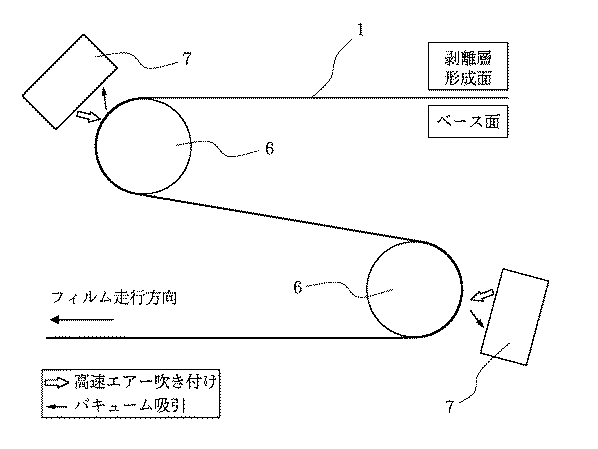
クリーニング方法としては、接触式、非接触式のいずれであってもよく、例えば、図1に示す接触式クリーニング法または図2に示す非接触式クリーニング法を用いることができる。図1および図2のいずれも上面側に剥離層が設けられたフィルムを搬送する様子を示している。図1に示すような接触式の場合、クリーニング材としては不織布が一般的であり、フィルムにキズが入らないよう注意して使用する。具体的には図示するように、不織布2をロール状に巻いた繰り出しロール3と、繰り出された不織布2を巻き取るための巻き取りロール4と、不織布2をフィルム1の表面に押し当てるためのガイドロール5とを有する装置を使用することが好ましい。この装置はフィルムの少なくとも剥離層形成側の面にのみ設置することが必要となるが、図1に示すように両面に設置することが好ましい。また、ガイドロール5はフィルム1に対する押し当て強さを調節可能なように位置を変えることができる構造であることが好ましく、位置を変えることにより、剥離層やポリエステルフィルム表面にキズが入らない範囲で、ダスト等を効率よく捕集することが容易となる。
【0017】
また、図2に示す非接触式の場合、図示するようにガイドロール6を介してフィルム1を搬送しつつ、例えば、ウェブクリーナー等のクリーニング装置7を用いてクリーニングを行う。図示するウェブクリーナーは高速エアー吹き付け機構とバキューム吸引機構とを備え、高速で空気を吹き付けてフィルム表面に付着した微粒子サイズのダストや異物を取り除き、これを吸引除去するタイプのクリーニング方法である。
【0018】
尚、図示するいずれのクリーニング方法も、積層チップコンデンサのように極めて小さいサイズで、しかも何層にも積層される製品の歩留まりの向上には極めて有効である。
【0019】
【実施例】
実施例1
〈剥離剤液の調製〉
以下に示す配合内容で、ビニル基を有するポリジメチルシロキサンとハイドロジェンシラン系化合物との混合物に白金系触媒を加えて付加反応させるタイプの硬化型シリコーン(信越化学工業(株)製・KS−847(H))をメチルエチルケトン(MEK)およびトルエンの混合溶剤中に溶解させ、全体の固形分濃度が3.0重量%の剥離剤液(シリコーン樹脂溶液)を調製した。
信越化学工業(株)製 商品名:KS−847H 300g
(固形分濃度30%、樹脂90g)
白金触媒CAT−PL−50T(信越化学工業(株)製) 3.0g
MEK/トルエン=50/50(重量比)溶液 2700g
【0020】
〈誘電体層塗料の調製〉
粒径0.1μm〜1.0μm程度のチタン酸バリウム、酸化クロム、酸化イットリウム、炭酸マンガン、炭酸バリウム、炭酸カルシウム、酸化硅素等の粉末を焼成した後、BaTiO3100モル%として、Cr2O3に換算して0.3モル%、MnOに換算して0.4モル%、BaOに換算して2.4モル%、CaOに換算して1.6モル%、SiO2に換算して4モル%、Y2O3に換算して0.1モル%の組成になるように混合し、ボールミルにより24時間混合して、乾燥後、誘電体原料を得た。この誘電体原料100重量部と、アクリル樹脂5重量部と、塩化メチレン40重量部と、アセトン25重量部と、ミネラルスピリット6重量部とを配合し、市販のφ10mmジルコニアビーズを用いてポット架台により24時間混合して、誘電体セラミック塗料(誘電体層塗料)を得た。
【0021】
〈剥離フィルムの作製〉
上記剥離剤液を、バーコーターにて、乾燥後の塗膜厚が0.15μmとなるように幅100mm、厚さ38μmの2軸延伸ポリエチレンテレフタレート(PET)フィルムに塗布し、加熱温度110℃で40秒間乾燥および硬化反応を行わせた。その後、図1に示す接触式クリーニング法にて不織布(富士紡績(株)製、POLYPAS)を使用してフィルムの両面のクリーニングを行ってから巻き取って、ロール状に巻回した剥離フィルムを得た。
【0022】
〈誘電体層の形成〉
次に、ドクターコート法を用いて、誘電体層塗料を、剥離フィルムの剥離剤液塗布面に乾燥後の誘電体層厚が8μmとなるように塗布し、70℃で20秒間乾燥した後ロール状に巻き取って、誘電体層(グリーンシート)を形成した。
【0023】
〈電極層の印刷〉
続いて、上記誘電体層上に、電極パターンを印刷した。電極には、ニッケル、銅を主成分とする材料を用いた。電極パターンは個々の電極が横方向及び縦方向に間隔を隔てて配列されているものとした。
【0024】
〈剥離・積層工程〉
以上の誘電体層形成工程および電極層印刷工程を実行した後、誘電体層および電極層を剥離フィルムから剥離した。このようにして得られた電極付きのグリーンシートを75枚作製して、これらを積層数75層にて積層した。
【0025】
〈積層セラミックチップ試料の作製〉
上述のようにして得られた積層グリーンシートを打ち抜き後プレスし、切断することにより、積層セラミックチップを得た。得られた積層セラミックチップを、280℃で12時間脱バインダし、還元雰囲気中で1300℃にて2時間焼成した。焼成後得られた積層体に端子電極を形成した。端子電極の材質は銅を主成分とした。これを窒素と水素の混合ガス雰囲気中で800℃にて30分間焼付けし、メッキを行って、積層セラミックチップ試料を得た。
【0026】
参考例1
接触式クリーニング法としての不織布の代わりに、図2に示す空気吹き付けタイプの非接触式クリーニング法(ウェブクリーナー)を用いた以外は実施例1と同様にして、積層セラミックチップ試料を作製した。
【0027】
実施例2
剥離層の形成工程において、1000mm幅のPETフィルムを用い、剥離層形成後一旦巻き取ったフィルムのロールをスリッターにて100mm幅に裁断した後、再度ロール状に巻き取る前に同様のクリーニングを行った以外は実施例1と同様にして、積層セラミックチップ試料を作製した。
【0028】
参考例2
剥離層の形成工程において、1000mm幅のPETフィルムを用い、剥離層形成後一旦巻き取ったフィルムのロールをスリッターにて100mm幅に裁断した後、再度ロール状に巻き取る前に同様のクリーニングを行った以外は参考例1と同様にして、積層セラミックチップ試料を作製した。
【0029】
比較例
クリーニングを全く行わなかった以外は実施例1と同様にして、積層セラミックチップ試料を作製した。
【0030】
ショート不良率
ヒューレットパッカード社製 高抵抗計HP−4329Aを用いて、20℃にて10V印加し、30秒後に抵抗値を測定した。絶縁抵抗が1000Ω以下のものをショート不良とし、各試料について、試験に供されたサンプル数に対するショート不良発生数の割合をショート不良率として表示した。この結果を下記の表1に示す。
【0031】
【表1】
【発明の効果】
以上説明してきたように、本発明の剥離フィルムの製造方法によれば、セラミックコンデンサの積層層間におけるダストや異物等の混入を適切に防止することにより、不良の発生率を飛躍的に低減することができる。
【図面の簡単な説明】
【図1】本発明に係る接触式クリーニング法の一実施例を示す概略図である。
【図2】本発明に係る非接触式クリーニング法の一実施例を示す概略図である。
【符号の説明】
1 フィルム
2 クリーニング材(不織布)
3 繰り出しロール
4 巻き取りロール
5,6 ガイドロール
7 クリーニング装置[0001]
BACKGROUND OF THE INVENTION
The present invention relates to a method for producing a release film, and more specifically, the occurrence rate of defects has been drastically reduced by appropriately removing dust and foreign matters mixed in the production process of a release film used for producing a ceramic capacitor. The present invention relates to a method for producing a release film.
[0002]
[Prior art]
A ceramic electronic component such as a ceramic capacitor is obtained by applying a ceramic coating containing ceramic powder, an organic binder, a plasticizer, a solvent, etc. on a flexible support (release film) by a doctor blade method or the like. A green ceramic dielectric sheet) is formed, and an electrode made of palladium, silver, nickel or the like is formed thereon by screen printing. In particular, when obtaining a ceramic capacitor having a laminated structure, the obtained green sheets are laminated one by one so as to have a desired laminated structure, and a ceramic green chip is obtained through a press cutting process. The binder in the ceramic green chip thus obtained was burned out and fired at 1000 ° C. to 1400 ° C., and terminal electrodes such as silver, silver-palladium, nickel, copper were formed on the obtained fired body. Get ceramic electronic parts.
[0003]
As another technique for manufacturing ceramic electronic components, a method of thermally transferring a green sheet so that the flexible support is on top (Japanese Patent Laid-Open No. 63-188926) or the like, There has been proposed a method for obtaining a laminate by repeating a step of forming a green sheet and a step of printing an electrode on the green sheet by a necessary number of laminations.
[0004]
[Problems to be solved by the invention]
As described above, contamination of contaminants such as dust and foreign matters is one of the major problems in the production of ceramic electronic components that require many steps of lamination, especially multilayer ceramic chip capacitors. This is one of the important precautions in manufacturing. A multilayer chip capacitor has a multilayer structure in which dielectric layers and electrode layers are alternately laminated as described above, and has a very small size of about several millimeters both vertically and horizontally. This is because even when dust or the like is mixed between the layers, the incidence of defective products becomes very high.
[0005]
Specifically, in the process of applying a ceramic paint on the release film to form a dielectric layer, and in the process of forming an electrode layer thereon, when dust or foreign matter adheres to the release layer, In a ceramic capacitor obtained by repeating the lamination process without removing them, the occurrence rate of short-circuit defects is increased.
[0006]
Accordingly, an object of the present invention is to produce a release film that can dramatically reduce the incidence of defects by eliminating the above-mentioned problems and appropriately preventing dust and foreign matter from being mixed between the multilayer layers of the ceramic capacitor. It is to provide a method.
[0007]
[Means for Solving the Problems]
In order to solve the above problems, a method for producing a release film for producing a ceramic capacitor according to the present invention comprises applying a release agent solution to at least one surface of a continuously conveyed polyester film, followed by drying and rolling. In the method for producing a release film including a step of winding the film, the polyester film release agent-coated surface is cleaned using a nonwoven fabric after the drying and before the roll-shaped winding. .
[0008]
Moreover, the manufacturing method of the peeling film for manufacturing the other ceramic capacitor | condenser of this invention applied the peeling agent liquid to at least one side of the polyester film conveyed continuously, it was made to dry, and it wound up in roll shape Then, in the manufacturing method of a peeling film including the process of cut | judging to predetermined width, after the said predetermined width | variety cutting, the release agent liquid application surface of the said polyester film is cleaned.
[0009]
In the method for producing a release film for producing the ceramic capacitor of the present invention, it is preferable to clean both surfaces of the polyester film.
[0010]
In accordance with the present invention, after the release layer is formed, the ceramic capacitor manufactured using a release film that has been cleaned at least on the surface to which the release agent solution is applied has a short circuit failure compared to the case of using the release film without cleaning. The occurrence rate can be significantly reduced.
[0011]
DETAILED DESCRIPTION OF THE INVENTION
Hereinafter, specific embodiments of the present invention will be described in detail.
In the present invention, a release agent solution such as a silicone resin is applied on a resin film such as a polyester film and dried to form a release layer, and then the release agent solution application surface of the polyester film is cleaned. As a result, it is possible to reliably prevent dust and foreign matter from entering the ceramic capacitor during manufacturing, which can cause a short-circuit defect, and to significantly reduce the defect occurrence rate.
[0012]
In the cleaning process, a polyester film is continuously conveyed, a release layer is formed on at least one side, and the release film is applied in a manufacturing process of a release film that is wound up in a roll, and is dried, preferably dried and cured. After forming the release layer, it is performed before winding into a roll. The wound roll is then transferred to a process provided separately, and is drawn out again, and used for a ceramic capacitor manufacturing process in which a dielectric layer and an electrode layer are formed on the release layer surface by coating and printing. Therefore, cleaning is most preferably performed immediately after winding after the release layer is formed.
[0013]
In addition, when the width of the device for applying the release film is wider than the width of the device for applying the dielectric layer, the release film is formed so as to match the application width of the dielectric layer after the release film is formed and wound. In this case, a slitting process for cutting to a width is performed. In this case, cleaning is performed after cutting to a predetermined width by the slitting process. This is because it is preferable to perform cleaning immediately before the coating process of the dielectric layer or the like as much as possible in order to surely eliminate the entry of dust and foreign matters.
[0014]
The polyester film (release film) after the release layer is formed needs to be cleaned on the surface on which the release agent solution is applied, but preferably on both sides. That is, when the release layer is formed on both sides, it is naturally necessary to clean both sides, but it is preferable to clean both sides even when the release layer is formed only on one side. In the case of one side, if only the surface on which the release layer is formed can be cleaned, dust and the like can be prevented to the minimum, but if dust or foreign matter adheres to the side where the release layer is not formed, take-up etc. Since the peeling layer may be contaminated again during the process, it is preferable to carry out both sides.
[0015]
A ceramic capacitor is formed by applying a ceramic coating on a release layer of a release film to form a dielectric layer, printing an electrode layer on the dielectric layer, and repeating this two-layer formation process at least once or more. The dielectric layer and the electrode layer are laminated on the release layer of the release film. In the present invention, preferably, as described above, after the release layer is formed, the surface of the release layer is cleaned immediately before winding. Therefore, it becomes effective cleaning.
[0016]
The cleaning method may be either a contact type or a non-contact type. For example, a contact type cleaning method shown in FIG. 1 or a non-contact type cleaning method shown in FIG. 2 can be used. Both FIG. 1 and FIG. 2 show how a film having a release layer provided on the upper surface side is conveyed. In the case of the contact type as shown in FIG. 1, a non-woven fabric is generally used as a cleaning material, and it is used with care so as not to scratch the film. Specifically, as shown in the figure, a
[0017]
In the case of the non-contact type shown in FIG. 2, cleaning is performed using a
[0018]
Note that any of the cleaning methods shown in the figure is extremely effective for improving the yield of a product having a very small size, such as a multilayer chip capacitor, and being stacked in layers.
[0019]
【Example】
Example 1
<Preparation of release agent solution>
A curable silicone of the type shown below, in which a platinum-based catalyst is added to a mixture of polydimethylsiloxane having a vinyl group and a hydrogensilane-based compound to cause an addition reaction (manufactured by Shin-Etsu Chemical Co., Ltd., KS-847) (H)) was dissolved in a mixed solvent of methyl ethyl ketone (MEK) and toluene to prepare a release agent solution (silicone resin solution) having a total solid content concentration of 3.0% by weight.
Product name: KS-847H 300g manufactured by Shin-Etsu Chemical Co., Ltd.
(Solid content concentration 30%, resin 90g)
Platinum catalyst CAT-PL-50T (manufactured by Shin-Etsu Chemical Co., Ltd.) 3.0 g
MEK / toluene = 50/50 (weight ratio) solution 2700 g
[0020]
<Preparation of dielectric layer paint>
After firing powders of barium titanate, chromium oxide, yttrium oxide, manganese carbonate, barium carbonate, calcium carbonate, silicon oxide and the like having a particle size of about 0.1 μm to 1.0 μm, BaTiO 3 is added as 100 mol% and Cr 2 O 0.3 mol% converted to 3 , 0.4 mol% converted to MnO, 2.4 mol% converted to BaO, 1.6 mol% converted to CaO, converted to SiO 2 4 mol%, Y 2 O 3 was converted to a composition of 0.1 mol%, mixed by a ball mill for 24 hours, and dried to obtain a dielectric material. 100 parts by weight of this dielectric material, 5 parts by weight of acrylic resin, 40 parts by weight of methylene chloride, 25 parts by weight of acetone, and 6 parts by weight of mineral spirits are blended with a commercially available φ10 mm zirconia bead. By mixing for 24 hours, a dielectric ceramic paint (dielectric layer paint) was obtained.
[0021]
<Preparation of release film>
The release agent solution was applied to a biaxially stretched polyethylene terephthalate (PET) film having a width of 100 mm and a thickness of 38 μm with a bar coater so that the coating thickness after drying was 0.15 μm, and the heating temperature was 110 ° C. The drying and curing reaction was performed for 40 seconds. Thereafter, the contact film cleaning method shown in FIG. 1 is used to clean the both surfaces of the film using a nonwoven fabric (Fujibo Co., Ltd., POLYPAS), and then wound up to obtain a release film wound into a roll. It was.
[0022]
<Formation of dielectric layer>
Next, using a doctor coat method, the dielectric layer coating is applied to the surface of the release film on which the release agent liquid is applied so that the thickness of the dielectric layer after drying is 8 μm, dried at 70 ° C. for 20 seconds, and then rolled. A dielectric layer (green sheet) was formed.
[0023]
<Printing the electrode layer>
Subsequently, an electrode pattern was printed on the dielectric layer. A material mainly composed of nickel and copper was used for the electrode. In the electrode pattern, the individual electrodes are arranged at intervals in the horizontal and vertical directions.
[0024]
<Peeling / Lamination process>
After performing the above dielectric layer forming step and electrode layer printing step, the dielectric layer and electrode layer were peeled from the release film. 75 green sheets with electrodes thus obtained were prepared, and these were laminated in a lamination number of 75 layers.
[0025]
<Preparation of multilayer ceramic chip sample>
The laminated green sheet obtained as described above was punched, pressed, and cut to obtain a laminated ceramic chip. The obtained multilayer ceramic chip was debindered at 280 ° C. for 12 hours and fired at 1300 ° C. for 2 hours in a reducing atmosphere. Terminal electrodes were formed on the laminate obtained after firing. The material of the terminal electrode was mainly copper. This was baked at 800 ° C. for 30 minutes in a mixed gas atmosphere of nitrogen and hydrogen, and plated to obtain a multilayer ceramic chip sample.
[0026]
Reference example 1
A multilayer ceramic chip sample was produced in the same manner as in Example 1 except that an air blowing type non-contact cleaning method (web cleaner) shown in FIG. 2 was used instead of the nonwoven fabric as the contact cleaning method.
[0027]
Example 2
In the step of forming the release layer, a 1000 mm width PET film was used, and after the release layer was formed, the roll of the film once wound was cut into a width of 100 mm with a slitter, and then the same cleaning was performed before winding it into a roll again. A multilayer ceramic chip sample was produced in the same manner as in Example 1 except that.
[0028]
Reference example 2
In the step of forming the release layer, a 1000 mm width PET film was used, and after the release layer was formed, the roll of the film once wound was cut into a width of 100 mm with a slitter, and then the same cleaning was performed before winding it into a roll again. A multilayer ceramic chip sample was produced in the same manner as in Reference Example 1 except for the above.
[0029]
Comparative example A multilayer ceramic chip sample was produced in the same manner as in Example 1 except that no cleaning was performed.
[0030]
Short-circuit defect rate Using a high resistance meter HP-4329A manufactured by Hewlett-Packard Company, 10V was applied at 20C, and the resistance value was measured after 30 seconds. Those having an insulation resistance of 1000Ω or less were regarded as short defects, and the ratio of the number of short defects occurring to the number of samples subjected to the test was displayed as the short defect rate for each sample. The results are shown in Table 1 below.
[0031]
[Table 1]
【Effect of the invention】
As described above, according to the method for producing a release film of the present invention, the occurrence rate of defects can be drastically reduced by appropriately preventing dust and foreign matters from being mixed between the laminated layers of ceramic capacitors. Can do.
[Brief description of the drawings]
FIG. 1 is a schematic view showing an embodiment of a contact cleaning method according to the present invention.
FIG. 2 is a schematic view showing an embodiment of a non-contact cleaning method according to the present invention.
[Explanation of symbols]
1
3 Feeding roll 4 Take-up rolls 5 and 6
Claims (3)
Priority Applications (2)
| Application Number | Priority Date | Filing Date | Title |
|---|---|---|---|
| JP2001296257A JP4919139B2 (en) | 2001-09-27 | 2001-09-27 | Method for producing release film for producing ceramic capacitor |
| TW91118445A TW542786B (en) | 2001-09-27 | 2002-08-15 | Method for manufacturing release film |
Applications Claiming Priority (1)
| Application Number | Priority Date | Filing Date | Title |
|---|---|---|---|
| JP2001296257A JP4919139B2 (en) | 2001-09-27 | 2001-09-27 | Method for producing release film for producing ceramic capacitor |
Publications (2)
| Publication Number | Publication Date |
|---|---|
| JP2003093964A JP2003093964A (en) | 2003-04-02 |
| JP4919139B2 true JP4919139B2 (en) | 2012-04-18 |
Family
ID=19117538
Family Applications (1)
| Application Number | Title | Priority Date | Filing Date |
|---|---|---|---|
| JP2001296257A Expired - Lifetime JP4919139B2 (en) | 2001-09-27 | 2001-09-27 | Method for producing release film for producing ceramic capacitor |
Country Status (2)
| Country | Link |
|---|---|
| JP (1) | JP4919139B2 (en) |
| TW (1) | TW542786B (en) |
Families Citing this family (5)
| Publication number | Priority date | Publication date | Assignee | Title |
|---|---|---|---|---|
| WO2006088758A2 (en) | 2005-02-14 | 2006-08-24 | Johnson & Johnson Vision Care, Inc. | A comfortable ophthalmic device and methods of its production |
| KR100983910B1 (en) | 2005-11-04 | 2010-09-28 | 도쿄 세이미츄 코퍼레이션 리미티드 | Film peeling method and film peeling apparatus |
| JP5423976B2 (en) * | 2010-03-29 | 2014-02-19 | Tdk株式会社 | Release film manufacturing method, ceramic component sheet manufacturing method, and ceramic component manufacturing method |
| JP2015228036A (en) * | 2015-07-24 | 2015-12-17 | 住友化学株式会社 | Foreign matter removal device |
| TWI651469B (en) | 2017-02-08 | 2019-02-21 | 吳樹木 | Air pumping device with automatic opening and closing air reservoir vent function |
Family Cites Families (4)
| Publication number | Priority date | Publication date | Assignee | Title |
|---|---|---|---|---|
| JPH05213506A (en) * | 1992-02-04 | 1993-08-24 | Mitsubishi Paper Mills Ltd | Dust removing method for web |
| JPH0991692A (en) * | 1995-09-26 | 1997-04-04 | Sony Corp | Surface treatment method and surface treatment apparatus for magnetic recording medium |
| JP2000006353A (en) * | 1998-06-25 | 2000-01-11 | Teijin Ltd | Mold release film |
| JP2000288483A (en) * | 1999-04-05 | 2000-10-17 | Fuji Photo Film Co Ltd | Dust removing method of long-length flexible sheet |
-
2001
- 2001-09-27 JP JP2001296257A patent/JP4919139B2/en not_active Expired - Lifetime
-
2002
- 2002-08-15 TW TW91118445A patent/TW542786B/en not_active IP Right Cessation
Also Published As
| Publication number | Publication date |
|---|---|
| TW542786B (en) | 2003-07-21 |
| JP2003093964A (en) | 2003-04-02 |
Similar Documents
| Publication | Publication Date | Title |
|---|---|---|
| US7518848B2 (en) | Electronic device and the production method | |
| KR100749792B1 (en) | Method for manufacturing multilayer unit for multilayer electronic component | |
| JP4919139B2 (en) | Method for producing release film for producing ceramic capacitor | |
| EP1612814A1 (en) | Production method for laminated ceramic electronic component | |
| WO2005117041A1 (en) | Electronic part, layered ceramic capacitor, and manufacturing method thereof | |
| KR100733141B1 (en) | Production method for laminated ceramic electronic component | |
| JP4354993B2 (en) | Manufacturing method of multilayer electronic component | |
| US7867349B2 (en) | Thick film green sheet slurry, production method of thick film green sheet slurry, production method of thick film green sheet and production methods of thick film green sheet and electronic device | |
| JP2003197457A (en) | Method for transferring metal film, and method for manufacturing electronic component having internal electrode | |
| KR20040078791A (en) | Film vapor deposition method | |
| CN114551101B (en) | Laminated electronic components | |
| JP2003071375A (en) | Producing method of strippable film | |
| CN100338153C (en) | Method for producing stripping thin film | |
| US20080257472A1 (en) | Method for manufacturing ceramic plates | |
| JP2005252039A (en) | Electronic component stack manufacturing device and manufacturing method of electronic component stack | |
| JP2004221304A (en) | Method for manufacturing electronic parts having internal electrode | |
| JP2002127117A (en) | Green sheet manufacturing method and electronic component manufacturing method | |
| JP4626455B2 (en) | Manufacturing method of multilayer electronic component | |
| JP2006278764A (en) | Manufacturing method of laminated ceramic electronic component | |
| KR100749796B1 (en) | Method for manufacturing multilayer unit for multilayer electronic component | |
| JPH01226132A (en) | Manufacture of electronic component of laminated ceramic | |
| JP4788446B2 (en) | Green sheet laminate and manufacturing method thereof, multilayer ceramic electronic component and manufacturing method thereof | |
| JP2003234241A (en) | Metal film transfer film for electronic parts | |
| JP2007123758A (en) | Manufacturing method for laminated electronic component | |
| JP2638044B2 (en) | Manufacturing method of multilayer ceramic electronic component |
Legal Events
| Date | Code | Title | Description |
|---|---|---|---|
| A621 | Written request for application examination |
Free format text: JAPANESE INTERMEDIATE CODE: A621 Effective date: 20080306 |
|
| A977 | Report on retrieval |
Free format text: JAPANESE INTERMEDIATE CODE: A971007 Effective date: 20101007 |
|
| A131 | Notification of reasons for refusal |
Free format text: JAPANESE INTERMEDIATE CODE: A131 Effective date: 20101015 |
|
| A521 | Written amendment |
Free format text: JAPANESE INTERMEDIATE CODE: A523 Effective date: 20101214 |
|
| A131 | Notification of reasons for refusal |
Free format text: JAPANESE INTERMEDIATE CODE: A131 Effective date: 20111014 |
|
| A521 | Written amendment |
Free format text: JAPANESE INTERMEDIATE CODE: A523 Effective date: 20111213 |
|
| TRDD | Decision of grant or rejection written | ||
| A01 | Written decision to grant a patent or to grant a registration (utility model) |
Free format text: JAPANESE INTERMEDIATE CODE: A01 Effective date: 20120106 |
|
| A01 | Written decision to grant a patent or to grant a registration (utility model) |
Free format text: JAPANESE INTERMEDIATE CODE: A01 |
|
| A61 | First payment of annual fees (during grant procedure) |
Free format text: JAPANESE INTERMEDIATE CODE: A61 Effective date: 20120119 |
|
| R150 | Certificate of patent or registration of utility model |
Ref document number: 4919139 Country of ref document: JP Free format text: JAPANESE INTERMEDIATE CODE: R150 Free format text: JAPANESE INTERMEDIATE CODE: R150 |
|
| FPAY | Renewal fee payment (event date is renewal date of database) |
Free format text: PAYMENT UNTIL: 20150210 Year of fee payment: 3 |