JP4906798B2 - Lens array, LED head, exposure apparatus, image forming apparatus, and reading apparatus - Google Patents
Lens array, LED head, exposure apparatus, image forming apparatus, and reading apparatus Download PDFInfo
- Publication number
- JP4906798B2 JP4906798B2 JP2008172823A JP2008172823A JP4906798B2 JP 4906798 B2 JP4906798 B2 JP 4906798B2 JP 2008172823 A JP2008172823 A JP 2008172823A JP 2008172823 A JP2008172823 A JP 2008172823A JP 4906798 B2 JP4906798 B2 JP 4906798B2
- Authority
- JP
- Japan
- Prior art keywords
- microlens
- light
- lens array
- lens
- optical axis
- Prior art date
- Legal status (The legal status is an assumption and is not a legal conclusion. Google has not performed a legal analysis and makes no representation as to the accuracy of the status listed.)
- Expired - Fee Related
Links
- 230000003287 optical effect Effects 0.000 claims description 87
- 239000011347 resin Substances 0.000 claims description 20
- 229920005989 resin Polymers 0.000 claims description 20
- 230000000712 assembly Effects 0.000 claims description 7
- 238000000429 assembly Methods 0.000 claims description 7
- 239000011247 coating layer Substances 0.000 claims description 2
- 239000000945 filler Substances 0.000 claims 3
- 239000011358 absorbing material Substances 0.000 claims 1
- 238000003384 imaging method Methods 0.000 description 18
- 238000012546 transfer Methods 0.000 description 16
- 239000000463 material Substances 0.000 description 10
- 230000015572 biosynthetic process Effects 0.000 description 8
- 238000010586 diagram Methods 0.000 description 8
- 238000001746 injection moulding Methods 0.000 description 8
- 230000031700 light absorption Effects 0.000 description 8
- 238000000465 moulding Methods 0.000 description 7
- 239000000654 additive Substances 0.000 description 6
- 230000000996 additive effect Effects 0.000 description 6
- 238000000034 method Methods 0.000 description 6
- 230000002093 peripheral effect Effects 0.000 description 6
- 230000032258 transport Effects 0.000 description 5
- 239000003365 glass fiber Substances 0.000 description 4
- 239000004734 Polyphenylene sulfide Substances 0.000 description 3
- 238000005520 cutting process Methods 0.000 description 3
- 230000000694 effects Effects 0.000 description 3
- 238000005259 measurement Methods 0.000 description 3
- 229920000069 polyphenylene sulfide Polymers 0.000 description 3
- 102100039856 Histone H1.1 Human genes 0.000 description 2
- 101001035402 Homo sapiens Histone H1.1 Proteins 0.000 description 2
- 230000007423 decrease Effects 0.000 description 2
- 238000007747 plating Methods 0.000 description 2
- 238000007740 vapor deposition Methods 0.000 description 2
- 230000000007 visual effect Effects 0.000 description 2
- 229920000049 Carbon (fiber) Polymers 0.000 description 1
- 102220616555 S-phase kinase-associated protein 2_E48R_mutation Human genes 0.000 description 1
- 239000004917 carbon fiber Substances 0.000 description 1
- 238000003486 chemical etching Methods 0.000 description 1
- 238000004140 cleaning Methods 0.000 description 1
- 239000011248 coating agent Substances 0.000 description 1
- 238000000576 coating method Methods 0.000 description 1
- 238000004891 communication Methods 0.000 description 1
- 150000001925 cycloalkenes Chemical class 0.000 description 1
- 238000011161 development Methods 0.000 description 1
- 238000009826 distribution Methods 0.000 description 1
- 238000011156 evaluation Methods 0.000 description 1
- 239000000835 fiber Substances 0.000 description 1
- 239000011521 glass Substances 0.000 description 1
- 239000010410 layer Substances 0.000 description 1
- 239000004973 liquid crystal related substance Substances 0.000 description 1
- 239000002184 metal Substances 0.000 description 1
- VNWKTOKETHGBQD-UHFFFAOYSA-N methane Chemical compound C VNWKTOKETHGBQD-UHFFFAOYSA-N 0.000 description 1
- 239000003973 paint Substances 0.000 description 1
- 239000000049 pigment Substances 0.000 description 1
- 239000004033 plastic Substances 0.000 description 1
- 238000007788 roughening Methods 0.000 description 1
- 238000012360 testing method Methods 0.000 description 1
Images


Classifications
-
- G—PHYSICS
- G02—OPTICS
- G02B—OPTICAL ELEMENTS, SYSTEMS OR APPARATUS
- G02B3/00—Simple or compound lenses
- G02B3/0006—Arrays
- G02B3/0037—Arrays characterized by the distribution or form of lenses
- G02B3/0056—Arrays characterized by the distribution or form of lenses arranged along two different directions in a plane, e.g. honeycomb arrangement of lenses
-
- B—PERFORMING OPERATIONS; TRANSPORTING
- B41—PRINTING; LINING MACHINES; TYPEWRITERS; STAMPS
- B41J—TYPEWRITERS; SELECTIVE PRINTING MECHANISMS, i.e. MECHANISMS PRINTING OTHERWISE THAN FROM A FORME; CORRECTION OF TYPOGRAPHICAL ERRORS
- B41J2/00—Typewriters or selective printing mechanisms characterised by the printing or marking process for which they are designed
- B41J2/435—Typewriters or selective printing mechanisms characterised by the printing or marking process for which they are designed characterised by selective application of radiation to a printing material or impression-transfer material
- B41J2/447—Typewriters or selective printing mechanisms characterised by the printing or marking process for which they are designed characterised by selective application of radiation to a printing material or impression-transfer material using arrays of radiation sources
- B41J2/45—Typewriters or selective printing mechanisms characterised by the printing or marking process for which they are designed characterised by selective application of radiation to a printing material or impression-transfer material using arrays of radiation sources using light-emitting diode [LED] or laser arrays
- B41J2/451—Special optical means therefor, e.g. lenses, mirrors, focusing means
-
- G—PHYSICS
- G02—OPTICS
- G02B—OPTICAL ELEMENTS, SYSTEMS OR APPARATUS
- G02B3/00—Simple or compound lenses
- G02B3/0006—Arrays
- G02B3/0037—Arrays characterized by the distribution or form of lenses
- G02B3/0062—Stacked lens arrays, i.e. refractive surfaces arranged in at least two planes, without structurally separate optical elements in-between
- G02B3/0068—Stacked lens arrays, i.e. refractive surfaces arranged in at least two planes, without structurally separate optical elements in-between arranged in a single integral body or plate, e.g. laminates or hybrid structures with other optical elements
-
- H—ELECTRICITY
- H04—ELECTRIC COMMUNICATION TECHNIQUE
- H04N—PICTORIAL COMMUNICATION, e.g. TELEVISION
- H04N1/00—Scanning, transmission or reproduction of documents or the like, e.g. facsimile transmission; Details thereof
- H04N1/024—Details of scanning heads ; Means for illuminating the original
- H04N1/028—Details of scanning heads ; Means for illuminating the original for picture information pick-up
- H04N1/03—Details of scanning heads ; Means for illuminating the original for picture information pick-up with photodetectors arranged in a substantially linear array
- H04N1/031—Details of scanning heads ; Means for illuminating the original for picture information pick-up with photodetectors arranged in a substantially linear array the photodetectors having a one-to-one and optically positive correspondence with the scanned picture elements, e.g. linear contact sensors
- H04N1/0311—Details of scanning heads ; Means for illuminating the original for picture information pick-up with photodetectors arranged in a substantially linear array the photodetectors having a one-to-one and optically positive correspondence with the scanned picture elements, e.g. linear contact sensors using an array of elements to project the scanned image elements onto the photodetectors
Landscapes
- Physics & Mathematics (AREA)
- Optics & Photonics (AREA)
- General Physics & Mathematics (AREA)
- Engineering & Computer Science (AREA)
- Toxicology (AREA)
- General Health & Medical Sciences (AREA)
- Health & Medical Sciences (AREA)
- Multimedia (AREA)
- Signal Processing (AREA)
- Facsimile Heads (AREA)
- Lens Barrels (AREA)
- Exposure Or Original Feeding In Electrophotography (AREA)
- Lenses (AREA)
- Printers Or Recording Devices Using Electromagnetic And Radiation Means (AREA)
Description
本発明は、画像形成装置や読取装置に具備されるレンズアレイ、該レンズアレイを具備する露光装置、該露光装置を具備するLEDヘッドおよび前記レンズアレイを具備する画像形成装置および読取装置に関する。 The present invention relates to a lens array included in an image forming apparatus or a reading apparatus, an exposure apparatus including the lens array, an LED head including the exposure apparatus, an image forming apparatus including the lens array, and a reading apparatus.
従来、複数のLED(発光ダイオード)をアレイ状に配列したLEDヘッドを使用する画像形成装置や、複数の受光素子をアレイ状に配列した受光部に原稿の像を結像させるスキャナやファクシミリ装置等の読取装置においては、光学系としてロッドレンズアレイが用いられている。ロッドレンズアレイは物体の正立等倍像をライン状に形成する光学系である。このような光学系では、解像度を高めるためにレンズの間に遮光手段を設けたものがあり、例えば、特開2005−122041号公報に開示されている。 Conventionally, an image forming apparatus using an LED head in which a plurality of LEDs (light emitting diodes) are arranged in an array, a scanner or a facsimile machine that forms an image of a document on a light receiving portion in which a plurality of light receiving elements are arranged in an array, etc. In this reading apparatus, a rod lens array is used as an optical system. The rod lens array is an optical system that forms an erecting equal-magnification image of an object in a line shape. In such an optical system, there is an optical system in which a light shielding unit is provided between lenses in order to increase resolution, and is disclosed in, for example, Japanese Patent Application Laid-Open No. 2005-122041.
一方、複数のマイクロレンズをアレイ状に配列し、物体の正立等倍像をライン状に形成する光学系を構成することができる。マイクロレンズによるレンズアレイにおいては、プラスチック射出成型により形状精度の高いレンズアレイを効率良く作成することができ、高い解像度を得ることができる。
しかしながら従来のレンズアレイにおいては、物体からの光線が結像として集光せずに結像面上に達する、いわゆるフレアが発生し、十分な解像度が得られなかった。このため従来のレンズアレイを用いた露光装置は十分なコントラストの結像が得られず、また画像形成装置においては、印刷画像にスジや濃淡ムラが発生していた。 However, in the conventional lens array, a so-called flare is generated in which light rays from an object reach the image plane without being condensed as an image, and sufficient resolution cannot be obtained. For this reason, the conventional exposure apparatus using the lens array cannot obtain an image with sufficient contrast, and in the image forming apparatus, streaks and shading unevenness occur in the printed image.
上記課題を解決するために本発明のレンズアレイは、複数のマイクロレンズが直線状に配列された複数のレンズ集合体と、絞りとしての開口部を複数有し、前記複数のレンズ集合体に対して該複数の開口部が前記複数のマイクロレンズにそれぞれ対向するように配設された遮光部材とを有し、前記レンズ集合体の各マイクロレンズの光軸はレンズ集合体間で対向するマイクロレンズの光軸に略一致するとともに各マイクロレンズの光軸は前記遮光部材の前記開口部を通過し、前記開口部に光を吸収する光吸収部を設け、前記光吸収部における可視光全域の全光反射率が0乃至3パーセントであり、前記レンズ集合体における前記マイクロレンズは、複数のレンズ列を形成するように配列され、前記レンズ列内の前記マイクロレンズの配列間隔をPY、前記レンズ列の配列間隔をPXとしたとき、PX<PYであり、
前記光吸収部は前記マイクロレンズの光軸方向に略平行な略帯状体であり、
前記マイクロレンズの焦点距離をFO、前記マイクロレンズと物体面との距離をLO、前記マイクロレンズの配列方向に略垂直で前記マイクロレンズの光軸に略垂直な方向における物体と前記光軸との距離をXO、前記マイクロレンズの配列方向に略垂直で前記光軸に略垂直な方向における物体と前記光吸収部との距離をXIとしたとき、
![]()
In order to solve the above problems, a lens array of the present invention has a plurality of lens assemblies in which a plurality of microlenses are arranged in a straight line, and a plurality of apertures as diaphragms, with respect to the plurality of lens assemblies. A plurality of openings are arranged so as to face the plurality of microlenses, and the optical axes of the microlenses of the lens assembly are opposed to each other between the lens assemblies. All of the optical axis of each microlens with substantially coincides with the optical axis passes through the opening of the shielding member, the light absorbing portion which absorbs light in the opening provided, the visible light region in the light-absorbing portion The light reflectance is 0 to 3%, and the microlenses in the lens assembly are arranged to form a plurality of lens rows, and the arrangement interval of the microlenses in the lens rows PY, when the PX an arrangement interval of the lens array, a PX <PY,
The light absorbing portion is a substantially strip-like body substantially parallel to the optical axis direction of the microlens,
The focal length of the microlens is FO, the distance between the microlens and the object plane is LO, and the object and the optical axis in a direction substantially perpendicular to the arrangement direction of the microlens and substantially perpendicular to the optical axis of the microlens. When the distance is XO and the distance between the object and the light absorbing portion in the direction substantially perpendicular to the arrangement direction of the microlenses and substantially perpendicular to the optical axis is XI,
![]()
上記構成の本発明によれば、遮光部材の開口部に光吸収部を設けたことにより、物体からの光線が結像として集光せずに結像面上に達する所謂フレアの発生を抑制することができ、解像度を向上させることができる。 According to the present invention having the above-described configuration, the light absorbing portion is provided in the opening of the light shielding member, thereby suppressing the generation of so-called flare that the light rays from the object reach the imaging plane without being condensed as the imaging. And the resolution can be improved.
以下、本発明の実施の形態を図面に従って説明する。なお各図面に共通する要素には同一の符号を付す。図1は本発明の実施例1に係る画像形成装置としての電子写真プリンタを示す概略構成図である。まず電子写真プリンタについて説明する。
Hereinafter, embodiments of the present invention will be described with reference to the drawings. In addition, the same code | symbol is attached | subjected to the element common to each drawing. FIG. 1 is a schematic configuration diagram showing an electrophotographic printer as an image forming apparatus according to
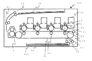
図1において、電子写真プリンタ100は、色材としての顔料を含む樹脂からなるトナーにより、画像データをもとに印字媒体上に画像を形成する。電子写真プリンタ100には、印字媒体としての用紙101を収納する給紙カセット60が装着され、用紙101を給紙カセット60から繰出す給紙ローラ61を備え、用紙101を搬送する搬送ローラ62、63が配置される。
In FIG. 1, an
実施例1における電子写真プリンタ100はカラー電子写真方式であり、電子写真プリンタ100内には、イエロー、マゼンダ、シアン、ブラックの各色の画像を形成する画像形成部が設けられている。各画像形成部は同様の構成をしており、画像形成部には、静電潜像担持体としての感光体ドラム41、感光体ドラム41の表面に電荷を供給して帯電させる帯電ローラ42、帯電された感光体ドラム41の表面に画像データをもとに選択的に光を照射して、静電潜像を形成する露光手段としてのLEDヘッド3、感光体ドラム41に形成された静電潜像をトナーにより現像し、トナー像を形成する現像器5、現像器5にトナーを供給するトナーカートリッジ51、さらに感光体ドラム41上に形成されたトナー像を用紙101上に転写する転写ローラ80および転写部を通過した後の感光体ドラム41の表面に残留したトナーを除去するクリーニングブレード43が配置される。
The
そして用紙101を搬送する転写ベルト81が画像形成部の下方に配設され、さらに用紙101上に転写されたトナー像を熱及び圧力で定着する定着器9が配置される。定着器9の左側には、定着器9を通過した用紙101を搬送する搬送ローラ64、画像が形成された印字媒体101が集積される排出部28に印字媒体101を排出する排出ローラ27が配置される。
A transfer belt 81 that conveys the
画像形成部の帯電ローラ42及び転写ローラ80には図示しない電源により所定の電圧が印加される。そして、転写ベルト81、感光体ドラム7及び各搬送用ローラはそれぞれ図示しないモータと図示しない駆動を伝えるギヤにより回転駆動される。さらに、現像器5、LEDヘッド3、定着器9及び図示しない各モータには、それぞれ電源及び制御装置が接続される。また電子写真プリンタ100には外部装置と通信を行い印刷データを受信する外部インターフェースが設けられ、さらに外部インターフェースから印刷データを受信し、電子写真プリンタ100全体の制御を行う制御部が設けられている。
A predetermined voltage is applied to the
次に本発明に係るLEDヘッドの構成について説明する。図2は本発明に係る露光装置としてのLEDヘッドを示す概略断面図である。図2において、LEDヘッド3にはレンズアレイ1が配置される。レンズアレイ1はホルダ34に固定されている。30は発光部としてのLED素子である。ドライバIC31はLED素子30の発光を制御する。LED素子30及びドライバIC31は配線基板33上に配置される。また、LED素子30は配列ピッチPD(mm)で1列の直線に配列される。LED素子30とドライバIC31はワイヤ32により結線される。41は静電潜像が形成される感光体ドラムである。
Next, the configuration of the LED head according to the present invention will be described. FIG. 2 is a schematic sectional view showing an LED head as an exposure apparatus according to the present invention. In FIG. 2, the
本実施例においては、LEDヘッド3は600dpi(dots per inch)の解像度を有し、LED素子30が1インチ当たり(1インチは約25.4mm)600個配置されている。すなわち、LED素子30の配列ピッチPDは0.0423mmである。
In the present embodiment, the
次に実施例1のレンズアレイの構成について説明する。図3は実施例1のレンズアレイを示す平面図、図4は実施例1のレンズアレイを示す断面図で、図3のA−Aで切断した断面図である。両図において、レンズアレイ1はレンズ集合体としての2個のレンズ板11a、11bと遮光部材13とからなる。図4に示すように、レンズアレイ1は、光軸が略一致するように配置されたレンズ板11aとレンズ板11bが、遮光部材13を間に挟んで配置した構成となっている。
Next, the configuration of the lens array of Example 1 will be described. 3 is a plan view showing the lens array of Example 1, and FIG. 4 is a cross-sectional view showing the lens array of Example 1. FIG. 3 is a cross-sectional view taken along line AA of FIG. In both figures, the
レンズ板11aには、図3に示すように、複数のマイクロレンズ12が間隔PYで配列され、さらにマイクロレンズ12の配列方向に直交する方向に間隔PXで2列に配列される。本実施例においては、PX<PYとなっている。マイクロレンズ12は半径RL、隣接する他の列のマイクロレンズ12との間隔はPNで、一部が隣接するマイクロレンズ12にオーバーラップするように配置される(PN<2RL)。マイクロレンズ12の面間隔すなわち両曲面の頂点間の距離はLT(図4に示す)である。レンズ板11aは発光部の光線を透過する素材により構成される。
On the lens plate 11a, as shown in FIG. 3, a plurality of
図5は遮光部材を示す平面図である。図4、図5において、遮光部材13は発光部の光線を遮光する素材により形成される。遮光部材13には絞りとしての開口部13aが筒状に形成されている。開口部13aの内壁部分は、全体が発光部の光線を吸収する光吸収部13bとして作用するように、日本工業規格(JIS B0601−1994)で定められた方法で測定した、マイクロレンズ12の光軸と略平行な方向で測定した算術平均粗さが所定の値となるように構成されている。
FIG. 5 is a plan view showing the light shielding member. 4 and 5, the
図6は開口部を示す平面図である。開口部13aの平面は、半径がRAの円筒形部分の軸より(PX−TB)/2の位置で軸に略平行な平面で仕切られた形状となっている。ここでTBは図5に示すように、2列の開口部13a間の間隔である。開口部13aの配列間隔は、図5に示すように、マイクロレンズ12の配列間隔に略一致して、間隔PYで形成され、さらにマイクロレンズ12の配列方向に直交する方向に間隔PXで2列に形成される。開口部13aの円筒形部分の軸がマイクロレンズ12の光軸と略一致するように配置される。遮光部材13の光軸方向の長さは図4に示すようにLSである。
FIG. 6 is a plan view showing the opening. The plane of the opening 13a has a shape partitioned by a plane substantially parallel to the axis at a position (PX-TB) / 2 from the axis of the cylindrical portion having a radius RA. Here, as shown in FIG. 5, TB is the distance between the two rows of
実施例1のレンズ板11a、11bは、シクロオレフィン系樹脂である光学樹脂(日本ゼオン社製、商品名;ZEONEX(ゼオネックス)E48R)を使用し、射出成形により複数のマイクロレンズ12を一体に成形した。マイクロレンズ12の各曲面は、下記数1で表される回転対称高次非球面で構成することにより、高い解像度を得ることができる。下記数1において、関数z(r)は、マイクロレンズ12の光軸に略平行な方向を軸とし、半径方向の座標をrとした回転座標系を示し、マイクロレンズ12の各曲面の頂点を原点とし、レンズアレイ1の物体面から結像面へ向かう方向を正の数で表す。Cは曲率半径、Aは非球面係数4次の係数、Bは非球面係数6次の係数を示す。
The lens plates 11a and 11b of Example 1 use an optical resin (trade name: ZEONEX E48R, manufactured by Nippon Zeon Co., Ltd.) which is a cycloolefin resin, and a plurality of

次にレンズアレイ1の詳細について図7を用いて説明する。図7はレンズアレイをマイクロレンズ12の配列方向に略平行で光軸を含む平面で切断した断面図であり、図面の左右方向はマイクロレンズ12の配列と平行な方向である。図7において、レンズアレイ1の物体面から距離LOだけ離れた位置に第1のマイクロレンズ(レンズ板11aに配設されたマイクロレンズ)12aが配置される。さらに、第2のマイクロレンズ(レンズ板11bに配設されたマイクロレンズ)12bが、第1のマイクロレンズ12aと光軸が略一致するように対向して、距離LSを隔てて配置される。レンズアレイ1の結像面は第2のマイクロレンズ12bから光軸方向に距離LI隔てた位置である。
Next, details of the
第1のマイクロレンズ12aは、厚みがLT1であり、前側焦点距離がFOであり、光軸方向に第1のマイクロレンズ12aから距離LO1の位置にある物体の像を、光軸方向に距離LI1離れた面に形成する。第2のマイクロレンズ12bは、後側焦点距離がFIであり、第2のマイクロレンズ12bから距離LO2の位置にある物体の像を、光軸方向に距離LI2隔てた位置に形成する。
The
レンズアレイ1の物体面(OP)から第1のマイクロレンズ12aまでの距離LOは距離LO1と等しく設定され、第1のマイクロレンズ12aと第2のマイクロレンズ12bの間隔LSは、LS=LI1+LO2に設定され、第2のマイクロレンズ12bからレンズアレイ1の結像面(IP)までの距離LIは、LI2と等しく設定される。
The distance LO from the object plane (OP) of the
なお、第1のマイクロレンズ12aと第2のマイクロレンズ12bを同じ構成のレンズとすることができる。この場合、第1のマイクロレンズ12aと第2のマイクロレンズ12bは、ともに厚みがLT1であり、前側焦点距離がFOであり、光軸方向に距離LO1の位置にある物体の像を、光軸方向に距離LI1離れた面に形成するとき、レンズアレイ1の物体面から第1のマイクロレンズ12aまでの距離LOは距離LO1と等しく設定され、第1のマイクロレンズ12aと第2のマイクロレンズ12bの間隔LSは、LS=2×LI1に設定され、第1のマイクロレンズ12aの物体面側の曲面と同じ形状の面が第2のマイクロレンズ12bの結像面側の曲面となるように対向して配置される。第2のマイクロレンズ12bからレンズアレイ1の結像面までの距離LIは、LO1と等しく設定され、LI=LOである。
The
次に実施例1の動作を説明する。まず画像形成装置としての電子写真プリンタ100の印刷動作を説明する。図1において、印刷動作が起動されると、感光体ドラム41の表面が図示しない電源装置により電圧が印加された帯電ローラ42により帯電される。続いて、感光体ドラム41が回転することによって、帯電された感光体ドラム41表面がLEDヘッド3の付近に到達すると、LEDヘッド3によって露光され、感光体ドラム41表面に静電潜像が形成される。静電潜像は現像器5により現像され、感光体ドラム41の表面にトナー像が形成される。
Next, the operation of the first embodiment will be described. First, the printing operation of the
一方、給紙カセット60に収納された用紙101が給紙ローラ61によって給紙カセット60から繰出され、搬送ローラ62、63により、転写ローラ80及び転写ベルト81の付近に搬送される。そして、感光体ドラム41が回転することによって、現像によって感光体ドラム41表面上に形成されたトナー像が転写ローラ80及び転写ベルト81の付近に到達すると、図示しない電源装置により電圧が印加されている転写ローラ80と転写ベルト81によって、感光体ドラム41表面上のトナー像が用紙101上に転写される。
On the other hand, the
各画像形成部においてトナー像が転写された用紙101は、転写ベルト81の回転によって、定着器9に搬送される。用紙101上のトナー像は定着器9により、加圧しながら過熱することにより溶融し、用紙101上に定着される。さらに用紙101は、搬送ローラ26及び排出ローラ27により、排出部28に排出され、電子写真プリンタ100の印刷動作が終了する。
The
次に、実施例1の露光装置の動作について図2を用いて説明する。図2において、画像データをもとに電子写真プリンタ100の制御部によりLEDヘッド3の制御信号が発信されると、図2のドライバIC31の制御信号により任意の光量でLED素子30が発光する。LED素子30からの光線はレンズアレイ1に入射し、感光体ドラム41上に結像が形成される。
Next, the operation of the exposure apparatus of Example 1 will be described with reference to FIG. In FIG. 2, when a control signal of the
次に、レンズアレイ1の動作について図7を用いて説明する。図7において、LED素子30の光線は第1のマイクロレンズ12aに入射し、第1のマイクロレンズ12aによって光軸27方向に距離LI1隔てた位置にある中間像面MIP上に中間像28が形成される。さらに第2のマイクロレンズ12bによって中間像の像が形成されることにより、結像面IP上にLED素子30の像が形成される。中間像はLED素子30の倒立縮小像であり、結像面上のLED素子30の像は中間像の第2のマイクロレンズ12bによる倒立拡大像である。また、第1のマイクロレンズ12aと第2のマイクロレンズ12bとの間では物体面上の各点からの光線の主光線25が略平行である、いわゆるテレセントリックになっている。このようにしてレンズアレイ1はLED素子30の正立等倍像を形成する。LED素子30からの光線のうち、結像に寄与しない光線は遮光部材13により遮断される。
Next, the operation of the
なお、第1のマイクロレンズ12aと第2のマイクロレンズ12bを同じ構成のレンズとした場合もレンズアレイ1はLED素子30の正立等倍像を形成する。この場合、LED素子30の光線は第1のマイクロレンズ12aに入射し、第1のマイクロレンズ12aによって光軸方向に距離(LS/2)隔てた位置の中間像面MIP上に中間像が形成される。さらに第2のマイクロレンズ12bによって中間像の像が形成されることにより、結像面上にLED素子30の像が形成される。また、第1のマイクロレンズ12aと第2のマイクロレンズ12bとの間ではテレセントリックになっている。
Even when the
次に、マイクロレンズ12の光学特性について、図8を用いて説明する。図8はレンズアレイをマイクロレンズ12の配列方向に略平行で光軸を含む平面で切断した断面図であり、図面の左右方向はマイクロレンズ12の配列と略平行な方向である。図8において、第1のマイクロレンズ12aの前側焦点距離はFOで、第1のマイクロレンズ12aの第1主平面H1−1から第1焦点面FP1−1までの距離がFOで、物体面までの距離はSOである。また、第2のマイクロレンズ12bの後側焦点距離はFIで、第2のマイクロレンズ12bの第2主平面H2−2から第2焦点面FP2−2までの距離がFIで、結像面までの距離はSIである。
Next, the optical characteristics of the
ここで、距離SOと距離LOの差は第1のマイクロレンズ12aの物体面側の曲面の曲率半径に反比例し、距離SIと距離LIの差は第2のマイクロレンズ12bの結像面側の曲面の曲率半径と反比例する。本実施例のレンズアレイ1においては、マイクロレンズ12の各曲面の曲率半径はともに大きく、距離SOと距離LOの差及び距離SIと距離LIの差はともに無視できて、SO≒LOかつSI≒LIである。
Here, the difference between the distance SO and the distance LO is inversely proportional to the radius of curvature of the curved surface on the object plane side of the
さらに、第1のマイクロレンズ12aと第2のマイクロレンズ12bとの間では物体面上の各点からの光線の主光線が光軸と略平行であり、特に遮光部材13の内壁の直近を通る光線(図8に示した光線20)の周辺光線は遮光部材13によって遮断されることと、図8に示した光線20と物体面と第1のマイクロレンズ12aの第1主平面の作る図形の相似関係とから、マイクロレンズ12の光軸27と遮光部材13の開口部13aの内壁との距離の最大値をRAとしたとき、第1のマイクロレンズ12aの視野半径RVは次式数2で示される。
Further, between the
![]()
![]()
次に従来のレンズアレイでの解像度低下について図11及び図12を用いて説明する。図11(a)と図11(b)は、それぞれ光軸の略一致する第1のマイクロレンズ12aと第2のマイクロレンズ12bと遮光部材13の開口部13aの一部と光軸から距離RVにあるLED素子30と光線を示した。図11(a)ではマイクロレンズ12の配列方向が図面左右の方向であり、光軸27が図面上下方向となっている。また、図11(b)では、マイクロレンズ12の配列方向が図面手前から奥の方向であり、光軸27が図面上下方向であり、レンズアレイ幅方向外側が図面右方向となっている。図11はマイクロレンズ12の視野内にあるLED素子30から光線が放射された場合を示す。
Next, resolution reduction in a conventional lens array will be described with reference to FIGS. 11A and 11B show the
図11(a)に示されたとおり、マイクロレンズ12の視野内にあるLED素子30から放射された光線の一部は、主光線25として第1焦点面FP1−1で光軸27と交差して第1のマイクロレンズ12aに入射し、光軸27に平行な光線として、開口部13aの内壁付近を通過して第2のマイクロレンズ12bに入射する。このとき、LED素子30から放射された光線の一部は、周辺光線26として第1のマイクロレンズ12aに入射し、中間像面MIPと開口部13aの交差する付近に像EGを形成する。
As shown in FIG. 11A, a part of the light beam emitted from the
また、図11(b)に示されたとおり、マイクロレンズ12の視野内にあるLED素子30から放射された光線の一部は、主光線25として第1焦点面FP1−1で光軸27と交差して第1のマイクロレンズ12aに入射し、光軸27に略平行な光線として、開口部13aの内壁付近を通過して第2のマイクロレンズ12bに入射する。このとき、LED素子30から放射された光線の一部は、周辺光線26として第1のマイクロレンズ12aに入射し、中間像面MIPと開口部13aの交差する付近であって、マイクロレンズ12の配列方向に略垂直でマイクロレンズ12の光軸27に略垂直な方向におけるLED素子30から距離XIの位置に像EGを形成する。
Further, as shown in FIG. 11B, a part of the light beam emitted from the
図12は、それぞれ光軸の略一致する第1のマイクロレンズ12aと第2のマイクロレンズ12bと開口部13aの一部と光軸から距離RVより遠方にある(マイクロレンズ12の視野外にある)LED素子30の光線を示した。図12(a)ではマイクロレンズ12の配列方向が図面左右の方向であり、光軸27が図面上下方向となっている。また、図12(b)では、マイクロレンズ12の配列方向が図面手前から奥の方向であり、光軸27が図面上下方向であり、レンズアレイ幅方向外側が図面右方向となっている。
In FIG. 12, the
図12(a)に示されたとおり、マイクロレンズ12の視野外にあるLED素子30から放射された光線の一部は、周辺光線26として第1のマイクロレンズ12aに入射し、中間像面MIPと第1のマイクロレンズ12aとに挟まれた領域の開口部13a上で像EGを形成する。
As shown in FIG. 12A, a part of the light beam emitted from the
また、図12(b)に示されたとおり、マイクロレンズ12の視野外にあるLED素子30から放射された光線の一部は、周辺光線26として第1のマイクロレンズ12aに入射し、中間像面MIPと第1のマイクロレンズ12aに挟まれた領域の開口部13a上であって、マイクロレンズ12の配列方向に略垂直でマイクロレンズ12の光軸27と略垂直な方向におけるLED素子30から距離XIの位置に像EGを形成する。主光線25はLED素子30の結像像を結像面上に形成する。従来のレンズアレイでは像EGの光線は開口部13a上で反射及び散乱して、第2のマイクロレンズ12bに入射し、結像面上に達し、LED素子30の結像と異なる結像面IP上の位置の光量を増加させ、レンズアレイの解像度を低下させるフレアとなっていた。
Further, as shown in FIG. 12B, a part of the light beam emitted from the
次に本実施例の光吸収部13bについて説明する。上述のように、本実施例では、遮光部材13の開口部13aの内壁に全面に渡って光吸収部13bが形成されている。本発明者らは、マイクロレンズ12の光軸27と略平行な方向における光吸収部13bの算術平均粗さがさまざまな値となるようにレンズアレイを形成し、評価したところ、算術平均粗さの値が2μm以上のときに、結像の解像度を低下させるフレアを十分抑制することができ、解像度の高いレンズアレイを構成することができた。就中、算術平均粗さの値が2μm乃至20μmとなるように形成したところ、フレアの光量を特に低く抑えることができ、レンズアレイによる結像の解像度を顕著に向上させることができた。
Next, the light absorption part 13b of a present Example is demonstrated. As described above, in this embodiment, the light absorbing portion 13b is formed over the entire inner wall of the
マイクロレンズ12の光軸27と略平行な方向における光吸収部13bの算術平均粗さがさまざまな値となるようにレンズアレイを形成し、評価したところ、算術平均粗さの値が2μm以上のときに、可視光全域の全光反射率がともに3%以下の値となった。さらに、算術平均粗さの値が2μm乃至20μmとなるように形成したところ、可視光全域の全光反射率がともに3%以下の値となった。すなわち、光吸収部13bの可視光全域の全光反射率が0乃至3%となるように構成することにより、像EGの光線の光吸収部13b上で反射が低く抑えられ、レンズアレイの解像度を低下させるほどにはフレアは発生しない。なお、可視光全域の全光反射率は、光吸収部13bを切り出し、光吸収部13b以外の面を、艶消し塗装して反射を無くし、光線入射角度45度の分光光度計(CM3700d、コニカミノルタ製)により可視光全域の全光線反射率を測定した。
When the lens array was formed and evaluated so that the arithmetic average roughness of the light absorbing portion 13b in the direction substantially parallel to the
図13には光吸収部材の算術平均粗さと可視光全域の全光反射率との関係が示され、図14には光吸収部材の算術平均粗さとレンズアレのMTFとの関係が示してある。ここでMTFとは、振幅伝達関数(Modulation Transfer Function)のことで、露光装置の解像度を示し、露光装置中で点灯しているLED素子の結像の光量のコントラストを示す。100%が結像のコントラストが最も大きく、露光装置としての解像度が高いことを示し、小さいほど光量のコントラストは小さく、露光装置としての解像度は低い。 FIG. 13 shows the relationship between the arithmetic average roughness of the light absorbing member and the total light reflectance over the entire visible light, and FIG. 14 shows the relationship between the arithmetic average roughness of the light absorbing member and the MTF of the lens array. Here, MTF is an amplitude transfer function (Modulation Transfer Function), which indicates the resolution of the exposure apparatus, and the contrast of the image formation light quantity of the LED elements that are lit in the exposure apparatus. 100% indicates that the imaging contrast is the highest and the resolution as the exposure apparatus is high. The smaller the contrast, the smaller the contrast of the light amount, and the lower the resolution as the exposure apparatus.
図13、図14からすると、(ア)算術平均粗さの値が2μm未満のとき、全光反射率が3%を超え、またレンズアレイのMTFが80%未満である。且つ、算術平均粗さの値を小さくするほど、全光反射率の値は大きくなり、またレンズアレイのMTFが小さくなることが分かる。(イ)算術平均粗さの値が2μm以上20μm以下の範囲では、算術平均粗さの値を大きくするほど、全光反射率の値は小さくなり、またレンズアレイのMTFは大きくなる。(ウ)算術平均粗さの値が20μmより大きい場合に、算術平均粗さの値の値を大きくするほど、全光反射率の値は小さくなり、レンズアレイのMTFは大きくなる傾向にあるが、算術平均粗さの値を20μmより大きくしようとすると、材料が金型内を流れず、射出成型で作成することができなかった。また、金型表面に粗面を形成して、遮光部材表面に転写しようとする場合には、算術平均粗さの値を20μmより大きくしようとすると、金型と遮光部材との離型抵抗が大きくなり、金型から遮光部材を取り出すことができなかった。従って、光吸収部材の算術平均粗さを2μm以上20μm以下の範囲にすることが望ましいことがわかる。 From FIG. 13 and FIG. 14, (a) when the value of arithmetic average roughness is less than 2 μm, the total light reflectance exceeds 3%, and the MTF of the lens array is less than 80%. It can also be seen that the smaller the arithmetic average roughness value, the larger the total light reflectance value and the smaller the MTF of the lens array. (A) In the range where the arithmetic average roughness value is 2 μm or more and 20 μm or less, the larger the arithmetic average roughness value, the smaller the total light reflectance value and the larger the MTF of the lens array. (C) When the arithmetic average roughness value is larger than 20 μm, the larger the arithmetic average roughness value, the smaller the total light reflectance value and the larger the MTF of the lens array. When trying to make the arithmetic mean roughness value larger than 20 μm, the material did not flow in the mold and could not be produced by injection molding. In addition, when a rough surface is formed on the mold surface and is to be transferred to the surface of the light shielding member, if the arithmetic average roughness value is made larger than 20 μm, the mold release resistance between the mold and the light shielding member is increased. It became large and the light shielding member could not be taken out from the mold. Therefore, it can be seen that the arithmetic average roughness of the light-absorbing member is preferably in the range of 2 μm to 20 μm.
一般に射出成型による樹脂の精密成型においては、添加剤の量や大きさによっては、金型内での樹脂の流動性が低下し、金型の細部に樹脂が流れ込まなかったり、成型後の樹脂の内部応力によって、成型後に大きく変形したりして、正確な形状で作成できないことがある。さらに、添加剤の量や大きさによっては、成型後にわずかに変形させただけで破壊されてしまう脆性が生ずる。 In general, in precision molding of resin by injection molding, depending on the amount and size of the additive, the fluidity of the resin in the mold decreases, and the resin does not flow into the details of the mold. Due to internal stress, it may be greatly deformed after molding, making it impossible to create an accurate shape. In addition, depending on the amount and size of the additive, brittleness may occur that can be destroyed by slight deformation after molding.
本実施例の遮光部材13に用いる樹脂に添加する添加剤としてのグラスファイバーの大きさを30μm乃至300μmとすると、遮光部材13の射出成型の工程において、金型内での樹脂の流動性が十分得られ、開口部13aの形状を正確に作成することができる。また、成型後の遮光部材13が脆性で無く強度が十分である。さらには、所望の算術平均粗さの値が得られ、フレアの光量を低く抑えることができ、レンズアレイによる結像の解像度を向上させることができる。
When the size of the glass fiber as an additive to be added to the resin used for the
また、本実施例の遮光部材13に用いる樹脂に添加する添加剤としてのグラスファイバーの添加量を樹脂100重量部に対し、グラスファイバー10重量部乃至100重量部とすると、金型内での樹脂の流動性が十分得られ、開口部13aの形状を正確に作成することができる。また、成型後の遮光部材13が脆性で無く強度が十分である。さらには、所望の算術平均粗さの値が得られ、フレアの光量を低く抑えることができ、レンズアレイによる結像の解像度を向上させることができる。さらには、添加剤としてグラスファイバーの他に同形状で同量の炭素繊維や樹脂を添加したところ、同様の効果が見られた。
Further, when the amount of glass fiber added as an additive to be added to the resin used in the
また、本実施例の遮光部材13を作成する金型を研削する工程で、金型表面の開口部13aの内壁に対応する箇所に凹凸を形成したところ、開口部13aの内壁の表面に粗面を形成することができ、光軸に略平行な方向の光吸収部13bの算術平均粗さの値が2μm以上のときに、結像の解像度を低下させるフレアを十分抑制することができ、解像度の高いレンズアレイを構成することができた。また、算術平均粗さの値が2μm乃至20μmとなるように形成したところ、フレアの光量を特に低く抑えることができ、レンズアレイによる結像の解像度を顕著に向上させることができた。
Further, in the step of grinding the mold for producing the
次にマイクロレンズ12の焦点距離FOの測定方法について説明する。図15はノーダルスライド法を用いた焦点距離測定器300を示す。焦点距離測定器300は、回転台301と顕微鏡302と光源303が配置される。回転台301は微小な角度で回転可能である。回転台301の回転中心301a位置は、顕微鏡302の光軸304上に配置される。回転台301は被検レンズ12を顕微鏡302の光軸304方向へ移動可能である。光源303は回転台301を挟んで、顕微鏡302の光軸304上に配置される。光源303は回転台301に対して略平行光線を照射する。
Next, a method for measuring the focal length FO of the
マイクロレンズ12の焦点距離の測定においては、まず最初に、図15(a)に示すように、顕微鏡302の物体面を回転台301の回転中心位置に合わせておく。測定するマイクロレンズ12を光軸27が顕微鏡302の光軸304に略一致するように回転台301上に配置する。顕微鏡302の物体面が光源303から遠ざかるように移動していくと、光源303の光線がマイクロレンズ12によって集光され、顕微鏡302の物体面にスポットを形成する。顕微鏡302の物体面上のマイクロレンズ12によって形成するスポットが最小であり、かつ回転台301を微小に回転させてもスポット径が変化しないような位置を探しながら、顕微鏡302の物体面とマイクロレンズ12とを各々の光軸方向へ移動する。
In measuring the focal length of the
顕微鏡302の物体面上のマイクロレンズ12によって形成するスポットが最小であり、かつ回転台301を微小に回転させてもスポット径が変化しないとき(図15(b)に示す場合)、回転台301の回転中心301aはマイクロレンズ12の主点28と略一致する。すなわち、マイクロレンズ12の第1主平面H1−1と光軸27の交点となる。また、顕微鏡302の物体面の位置はマイクロレンズ12の焦点位置Fである。従って、マイクロレンズ12の焦点距離FOは回転台301の回転中心301aと顕微鏡302の物体面との距離から求められる。
When the spot formed by the
本実施例のLEDヘッドについて、露光像の解像度を示すMTFを測定したところ、80%以上の値を示した。MTF(%)は露光像の光量の最大値EMAX、隣り合う2つの露光像の間の光量の最小値をEMINとしたとき、次式数7 のように定義される。 When the MTF indicating the resolution of the exposure image was measured for the LED head of this example, it showed a value of 80% or more. MTF (%) is defined by the following equation (7), where the maximum value EMAX of the light amount of the exposure image is EMAX and the minimum value of the light amount between two adjacent exposure images is EMIN.
![]()
![]()
次に実施例1のレンズアレイを用いたカラー電子写真プリンタを使用して得られた画像を評価したところ、筋や濃淡斑のない良好な画像が得られた。カラー電子写真プリンタの画像の評価は、印字領域全面に図16に示した全画素のうち1つおきにドットを形成する画像を形成し、画像品質の良否を評価した。図16において黒ドットは印字ドットを示し、白ドットは非印字ドットを示す。 Next, when an image obtained using a color electrophotographic printer using the lens array of Example 1 was evaluated, a good image free of streaks and shading was obtained. The image of the color electrophotographic printer was evaluated by forming an image in which every other pixel shown in FIG. 16 forms dots on the entire print area and evaluating the quality of the image. In FIG. 16, black dots indicate print dots, and white dots indicate non-print dots.
MTFの値が80%より大きいと筋や濃淡斑のない良好な印字ができたが、MTFの値が80%より小さいと筋や濃淡斑のあった画像ができてしまい、印字が良好でなくなり、その原因としては、本来、印刷画像でトナーが乗らない部分は、静電潜像においては電位が十分に高くなければならず、LEDヘッドで形成される像では暗くなければならないが、MTFの値が80%より小さいと、LEDヘッドで形成される像においては、暗くなければならない部分にも光線が入射し、静電潜像においては電位が十分に高くなければならないところの電位が下がり、トナーが付着してしまうためであると考えられる。 If the MTF value is greater than 80%, good printing without streaks and shading has been achieved, but if the MTF value is less than 80%, an image with streaks and shading will be produced, resulting in poor printing. The reason is that the portion of the printed image where the toner is not placed should have a sufficiently high potential in the electrostatic latent image and dark in the image formed by the LED head. If the value is less than 80%, in the image formed by the LED head, the light beam also enters the part that must be dark, and in the electrostatic latent image, the potential where the potential must be sufficiently high is lowered, This is probably because the toner adheres.
以上説明した実施例1においては、マイクロレンズ12を回転対称高次非球面で構成したが、マイクロレンズの形状はこれに限られない。例えば、アナモフィック非球面や放物面、楕円面、双曲面、コーニック面等の曲面を形成しても良い。また、レンズ板11a、11bは金型に作成された形状を樹脂に転写して形成されているが、樹脂を型に用いてもよく、切削加工により形成しても良い。さらに、レンズ板11a、11bの素材として樹脂を用いているが、ガラスを用いてもよい。また本実施例において、光吸収部13bの可視光全域の全光反射率が0乃至3%となるように構成したが、光吸収部13bにおける光源の光線の反射率を0乃至3%となるように設定してもよい。
In the first embodiment described above, the
また実施例1において、焦点距離FOの測定は、ノーダルスライド法を用いた焦点測定器を用いることに限定されない。さらに、焦点距離に換算可能な数値を測定しても良い。また遮光部材13はPPSを用いて作成したが、他の材料を用いてもよい。また、遮光部材13は射出成型により作成したが、その他の樹脂成型法を用いてもよく、さらには、切削加工や化学エッチングにより作成しても良い。また、光吸収部13bには、光線を吸収する材料で構成された塗料や鍍金や蒸着による被覆層を形成しても良い。また、発光部としてLED素子30を複数配置したLEDアレイを用いたが、例えば有機ELを発光部にしても良く、半導体レーザーを用いても良く、さらには蛍光灯やハロゲンランプ等の発光部に液晶素子で構成されたシャッターを併用した露光装置でも良い。
In the first embodiment, the measurement of the focal length FO is not limited to using a focus measuring device using the nodal slide method. Furthermore, a numerical value that can be converted into a focal length may be measured. The
以上のように実施例1によれば、レンズアレイ1の遮光部材13の開口部13aに光吸収部13bを設けたので、光源からの光線が結像として集光せずに結像面上に達する、いわゆるフレアの発生を抑えることができ、解像度を向上させることができる効果を奏する。
As described above, according to the first embodiment, since the light absorbing portion 13b is provided in the
次に実施例2について説明する。実施例2においては、光吸収部は、開口部13aの内壁の一部に形成される。図17は実施例2のレンズアレイの遮光部材を示す分解斜視図である。図17では、遮光部材13が開口部13aの円筒形部分の軸と略平行な平面で分解され、開口部13aの内壁上の一部に形成した光吸収部13cの形状及び位置が図示されている。光吸収部13cは開口部13aの円筒形部分の軸と略平行、すなわちマイクロレンズ12の光軸と略平行な略帯状である。
Next, Example 2 will be described. In the second embodiment, the light absorbing portion is formed on a part of the inner wall of the
図18は実施例2の遮光部材13に形成された開口部13aを示す平面図である。図18において、開口部13aの配列方向は図面上下方向であり、開口部13aは図面左右の方向に2列に配置される。マイクロレンズ12の光軸27方向は図面手前から奥の方向である。開口部13aの内側の2箇所に光吸収部13cが前記配列方向に対向するように設けられている。
FIG. 18 is a plan view showing the
図19は図18のC−C断面図、図20は図18のD−D断面図である。図19、図20に示したとおり、実施例2の光吸収部13cは、光軸方向には、開口部13aの第1のマイクロレンズ12a側の端部から中間像面MIPをやや通り過ぎた位置までに渡り、光軸方向に直交する方向には、LED素子30から距離XI離れた位置に配置される。本実施例の遮光部材13は、樹脂の射出成型により作成した。また光吸収部13cは、金型の一部に粗面化部を形成し、形状を樹脂に転写することにより、開口部13aの内壁の一部を粗面化し、光吸収部13cとした。
19 is a cross-sectional view taken along the line CC in FIG. 18, and FIG. 20 is a cross-sectional view taken along the line DD in FIG. As shown in FIGS. 19 and 20, the light absorbing portion 13 c of Example 2 is a position slightly passing through the intermediate image plane MIP from the end of the opening 13 a on the
実施例2のレンズアレイの動作は実施例1と同様である。
ここで実施例2の光吸収部13cが設けられる位置について、実施例1の図11を用いて説明する。図11(b)に示されたとおり、LED素子30から放射された光線の一部は、主光線25として第1焦点面FP1−1で光軸27と交差して第1のマイクロレンズ12aに入射し、光軸27に略平行な光線として、開口部13aの内壁付近を通過して第2のマイクロレンズ12bに入射する。このとき、LED素子30から放射された光線の一部は、周辺光線26として第1のマイクロレンズ12aに入射し、中間像面MIPと開口部13aの交差する付近であって、マイクロレンズ12の配列方向と略垂直でマイクロレンズ12の光軸27と略垂直な方向におけるLED素子30からXIの位置に像EGを形成する。
The operation of the lens array of the second embodiment is the same as that of the first embodiment.
Here, the position where the light absorbing portion 13c of the second embodiment is provided will be described with reference to FIG. 11 of the first embodiment. As shown in FIG. 11B, a part of the light beam emitted from the
図11(b)より、主光線25と光軸27と物体面OPと第1主平面H1−1に囲まれた2つの三角形の相似の関係と、SO≒LOとから、次式数8が得られる。
From FIG. 11B, from the similar relationship of two triangles surrounded by the
![]()
![]()
![]()
![]()
![]()
![]()
また、光吸収部13cを光線を吸収する材料を塗料として塗布したり、鍍金したり、蒸着するなどして光吸収層を形成することもできる。本実施例では、光吸収部13cを作成する領域を小さくできるので、効率よく作成できる。 The light absorbing layer 13c can also be formed by applying a material that absorbs light as a paint, plating, or vapor deposition. In the present embodiment, the area for creating the light absorbing portion 13c can be reduced, so that it can be created efficiently.
以上説明したように実施例2によれば、実施例1と同様に、物体からの光線が結像として集光せずに結像面上に達する、いわゆるフレアの発生を抑えることができ、解像度を向上させることができるという効果に加えて、光吸収部13cを作成する領域を小さくできるので、光吸収部を効率的に作成することができ、レンズアレイの生産性を向上させることができる。 As described above, according to the second embodiment, as in the first embodiment, it is possible to suppress the occurrence of so-called flare in which light rays from an object reach the image plane without focusing as an image. In addition to the effect that the light absorption part 13c can be made small, the light absorption part can be made efficiently and the productivity of the lens array can be improved.
次に実施例3について説明する。実施例3は読取装置におけるレンズアレイに係るものである。図21は実施例3のレンズアレイが適用される読取装置を示す概略構成図である。 Next, Example 3 will be described. Example 3 relates to a lens array in a reading apparatus. FIG. 21 is a schematic configuration diagram illustrating a reading device to which the lens array according to the third exemplary embodiment is applied.
図21において、500は、原稿の電子データを生成する読取装置としてのスキャナである。スキャナ500には、読取ヘッド400、原稿台502、レース503、滑車504、駆動ベルト505およびモータ506が設けられている。読取ヘッド400は原稿表面で反射した光線を取り込み電子データに変換する。読取ヘッド400はレール503上に移動可能に配置される。読み取りが行われる原稿507は原稿台502上に置かれる。原稿台502は可視光線を透過する素材で構成される。読取ヘッド400には照明装置としてのランプ501が設けられ、ランプ501で照射された光が原稿表面で反射し、読取ヘッド400内に取り込まれるよう配置される。また駆動ベルト505は、複数の滑車504により張架され、駆動ベルト505の一部は読取ヘッド400の一部に接続される。駆動ベルト505はモータ506により駆動され、読取ヘッド400を移動させる。
In FIG. 21, reference numeral 500 denotes a scanner as a reading device that generates electronic data of a document. The scanner 500 is provided with a
次に図22を用いて読取ヘッド400の構成を説明する。図22は読取ヘッドの構成を示す構成図である。図22において、402は原稿507で反射された光線の光路を折り曲げるミラーである。レンズアレイ403は原稿画像の結像を形成する。ラインセンサ401は複数の受光素子が間隔PRで直線状に配置されており、原稿画像の結像を電気信号に変換する。レンズアレイ403は遮光部材413と遮光部材413を挟んでその両側に配設されたマイクロレンズ412a、412bとにより構成される。
Next, the configuration of the
また実施例3の読取ヘッド400の構成と物体面(原稿)との配置を図23に示した。図23において、実施例3のレンズアレイ403の構成は実施例1及び実施例2のものと同様である。本実施例においては、ラインセンサ401は600dpiの解像度であり、受光素子が1インチ当たり(1インチは約25.4mm)600個配置されている。すなわち、受光素子の間隔PRが0.0423mmである。
FIG. 23 shows the configuration of the read
次に実施例3の動作を説明する。図21において、ランプ501が点灯し原稿507の表面を照射することにより、原稿表面で反射した光線が読取ヘッド400内に取り込まれる。モータ506により駆動ベルト505が駆動され、読取ヘッド400とランプ501が図面の左右方向に移動し、読取ヘッド400は、原稿507全面から反射した光線を取り込む。
Next, the operation of the third embodiment will be described. In FIG. 21, the
次に図22にしたがって読取ヘッド400の動作を説明する。原稿507で反射された光線は原稿台502を透過し、ミラー402により光路が折り曲げられ、レンズアレイ403に入射する。レンズアレイ403により結像された原稿画像の結像はラインセンサ401上に形成される。ラインセンサ401は形成された原稿画像の結像を電気信号に変換する。
Next, the operation of the read
実施例3のスキャナ500を用いて原稿507から画像データを形成したところ、原稿507と同一の良好な画像データが得られた。実施例3のスキャナ500を用いて読み取った原稿507は、図16におけるドットの間隔PD=0.0423mm、解像度600dpiとしたものである。つまり、PD=0.0423mm、解像度600dpiの全ドットのうち、1つおきにドットを形成した画像を媒体上の印字領域全面に形成した原稿を用いた。
When image data was formed from the
本実施例においては、原稿画像を電子データに変換する読取装置としてのスキャナを例に説明したが、光学的信号を電気的信号に変換するセンサやスイッチ、及びそれらを用いた入出力装置、生態認証装置、通信装置あるいは寸法測定器にも本発明は適用可能である。本実施例のレンズアレイを用いることにより、コントラストが高く、焦点深度が高く、十分な明るさの原稿画像の結像を形成することができる。また、本実施例の読取装置によって原稿と同一の画像データを得ることができた。 In this embodiment, a scanner as a reading device that converts an original image into electronic data has been described as an example. However, sensors and switches that convert optical signals into electric signals, input / output devices using them, The present invention can also be applied to an authentication device, a communication device, or a dimension measuring device. By using the lens array of this embodiment, it is possible to form an image of a document image with high contrast, high focal depth, and sufficient brightness. Also, the same image data as that of the original can be obtained by the reading apparatus of this embodiment.
1 レンズアレイ
3 LEDヘッド
11a、11b レンズ板
12a、12b マイクロレンズ
13 遮光部材
13a 開口部
13b、13c 光吸収部
30 LED素子
100 電子写真プリンタ
500 スキャナ
DESCRIPTION OF
Claims (15)
絞りとしての開口部を複数有し、前記複数のレンズ集合体に対して該複数の開口部が前記複数のマイクロレンズにそれぞれ対向するように配設された遮光部材とを有し、
前記レンズ集合体の各マイクロレンズの光軸はレンズ集合体間で対向するマイクロレンズの光軸に略一致するとともに各マイクロレンズの光軸は前記遮光部材の前記開口部を通過し、
前記開口部に光を吸収する光吸収部を設け、
前記光吸収部における可視光全域の全光反射率が0乃至3パーセントであり、
前記レンズ集合体における前記マイクロレンズは、複数のレンズ列を形成するように配列され、前記レンズ列内の前記マイクロレンズの配列間隔をPY、前記レンズ列の配列間隔をPXとしたとき、PX<PYであり、
前記光吸収部は前記マイクロレンズの光軸方向に略平行な略帯状体であり、
前記マイクロレンズの焦点距離をFO、前記マイクロレンズと物体面との距離をLO、前記マイクロレンズの配列方向に略垂直で前記マイクロレンズの光軸に略垂直な方向における物体と前記光軸との距離をXO、前記マイクロレンズの配列方向に略垂直で前記光軸に略垂直な方向における物体と前記光吸収部との距離をXIとしたとき、
A plurality of apertures as a diaphragm, and a plurality of lens aggregates, the plurality of apertures being arranged so as to face the plurality of microlenses, respectively,
The optical axis of each microlens of the lens assembly substantially coincides with the optical axis of the microlens facing between the lens assemblies, and the optical axis of each microlens passes through the opening of the light shielding member,
A light absorbing part that absorbs light is provided in the opening,
The total light reflectance of the entire visible light in the light absorbing portion is 0 to 3%,
The microlenses in the lens assembly are arranged so as to form a plurality of lens rows. When the arrangement interval of the microlenses in the lens row is PY and the arrangement interval of the lens rows is PX, PX < PY,
The light absorbing portion is a substantially strip-like body substantially parallel to the optical axis direction of the microlens,
The focal length of the microlens is FO, the distance between the microlens and the object plane is LO, and the object and the optical axis in a direction substantially perpendicular to the arrangement direction of the microlens and substantially perpendicular to the optical axis of the microlens. When the distance is XO and the distance between the object and the light absorbing portion in the direction substantially perpendicular to the arrangement direction of the microlenses and substantially perpendicular to the optical axis is XI,
絞りとしての開口部を複数有し、前記複数のレンズ集合体に対して該複数の開口部が前記複数のマイクロレンズにそれぞれ対向するように配設された遮光部材とを有し、
前記レンズ集合体の各マイクロレンズの光軸はレンズ集合体間で対向するマイクロレンズの光軸に略一致するとともに各マイクロレンズの光軸は前記遮光部材の前記開口部を通過し、
前記開口部に光を吸収する光吸収部を設け、
前記光吸収部における可視光全域の全光反射率が0乃至3パーセントであり、
前記レンズ集合体における前記マイクロレンズは、複数のレンズ列を形成するように配列され、前記レンズ列内の前記マイクロレンズの配列間隔をPY、前記レンズ列の配列間隔をPXとしたとき、PX<PYであり、
前記光吸収部は前記マイクロレンズの光軸方向に略平行な略帯状体であり、
前記マイクロレンズは該マイクロレンズの光軸に対して略垂直な方向に配列間隔PXで2列に配列され、前記マイクロレンズの焦点距離をFO、前記マイクロレンズと物体面との距離をLO、前記マイクロレンズの配列方向に略垂直で前記光軸に略垂直な方向における物体と前記光吸収部との距離をXIとしたとき、
A plurality of apertures as a diaphragm, and a plurality of lens aggregates, the plurality of apertures being arranged so as to face the plurality of microlenses, respectively,
The optical axis of each microlens of the lens assembly substantially coincides with the optical axis of the microlens facing between the lens assemblies, and the optical axis of each microlens passes through the opening of the light shielding member,
A light absorbing part that absorbs light is provided in the opening,
The total light reflectance of the entire visible light in the light absorbing portion is 0 to 3%,
The microlenses in the lens assembly are arranged so as to form a plurality of lens rows. When the arrangement interval of the microlenses in the lens row is PY and the arrangement interval of the lens rows is PX, PX < PY,
The light absorbing portion is a substantially strip-like body substantially parallel to the optical axis direction of the microlens,
The microlenses are arranged in two rows at an arrangement interval PX in a direction substantially perpendicular to the optical axis of the microlens, the focal length of the microlens is FO, the distance between the microlens and the object plane is LO, When the distance between the object and the light absorbing portion in the direction substantially perpendicular to the arrangement direction of the microlenses and substantially perpendicular to the optical axis is XI,
ンズアレイ。 The lens array according to claim 1, wherein a light beam reflectance of the light source in the light absorbing portion is 0 to 3 percent.
Priority Applications (2)
| Application Number | Priority Date | Filing Date | Title |
|---|---|---|---|
| JP2008172823A JP4906798B2 (en) | 2008-07-01 | 2008-07-01 | Lens array, LED head, exposure apparatus, image forming apparatus, and reading apparatus |
| US12/458,015 US7957067B2 (en) | 2008-07-01 | 2009-06-29 | Lens array, LED head, exposure device, image forming apparatus and reading apparatus |
Applications Claiming Priority (1)
| Application Number | Priority Date | Filing Date | Title |
|---|---|---|---|
| JP2008172823A JP4906798B2 (en) | 2008-07-01 | 2008-07-01 | Lens array, LED head, exposure apparatus, image forming apparatus, and reading apparatus |
Publications (2)
| Publication Number | Publication Date |
|---|---|
| JP2010014824A JP2010014824A (en) | 2010-01-21 |
| JP4906798B2 true JP4906798B2 (en) | 2012-03-28 |
Family
ID=41464158
Family Applications (1)
| Application Number | Title | Priority Date | Filing Date |
|---|---|---|---|
| JP2008172823A Expired - Fee Related JP4906798B2 (en) | 2008-07-01 | 2008-07-01 | Lens array, LED head, exposure apparatus, image forming apparatus, and reading apparatus |
Country Status (2)
| Country | Link |
|---|---|
| US (1) | US7957067B2 (en) |
| JP (1) | JP4906798B2 (en) |
Families Citing this family (9)
| Publication number | Priority date | Publication date | Assignee | Title |
|---|---|---|---|---|
| KR101728464B1 (en) * | 2010-05-11 | 2017-04-19 | 에스프린팅솔루션 주식회사 | Lens array, linear light exposure device, optical apparatus employing the linear light exposure unit |
| JP2012230252A (en) * | 2011-04-26 | 2012-11-22 | Oki Data Corp | Lens array, lens unit, exposure device, image forming apparatus, and reader |
| CN103975436B (en) | 2011-07-19 | 2019-05-10 | 新加坡恒立私人有限公司 | Methods of making passive optical devices and devices containing the same |
| US9461024B2 (en) * | 2013-08-01 | 2016-10-04 | Cree, Inc. | Light emitter devices and methods for light emitting diode (LED) chips |
| WO2016026680A1 (en) | 2014-08-20 | 2016-02-25 | Cassantec Ag | Malfunction prediction for components and units of technical entities |
| US10685288B2 (en) | 2014-08-20 | 2020-06-16 | Cassantec Ag | Configuration of malfunction prediction for components and units of technical entities |
| EP3286549A4 (en) | 2015-04-22 | 2019-04-17 | Shenzhen Genorivision Technology Co., Ltd. | BIOSENSOR |
| WO2021044573A1 (en) * | 2019-09-05 | 2021-03-11 | 三菱電機株式会社 | Image reading device |
| US11807220B1 (en) | 2023-05-30 | 2023-11-07 | Geotab Inc. | Method for capturing voltage-based events in motor vehicles |
Family Cites Families (9)
| Publication number | Priority date | Publication date | Assignee | Title |
|---|---|---|---|---|
| JPH06252450A (en) * | 1993-02-23 | 1994-09-09 | Kyocera Corp | Imaging device |
| US5796522A (en) * | 1996-12-20 | 1998-08-18 | Eastman Kodak Company | Lenslet array system with a baffle structure and a shutter |
| JPH10210213A (en) * | 1997-01-24 | 1998-08-07 | Fujitsu Ltd | Optical device |
| US6707613B2 (en) * | 2000-04-05 | 2004-03-16 | Rohm Co., Ltd. | Lens array unit and method of forming image |
| JP4495942B2 (en) | 2003-10-20 | 2010-07-07 | リコー光学株式会社 | Imaging optical system, image forming apparatus, printer and image reading apparatus |
| JP2006030722A (en) * | 2004-07-20 | 2006-02-02 | Alps Electric Co Ltd | Lens array for optical reading and its manufacturing method |
| US20100128353A1 (en) * | 2005-10-06 | 2010-05-27 | Nippon Sheet Glass Company, Limited | Imaging optical system, image reading apparatus and image reading apparatus using the imaging optical system |
| JP4402674B2 (en) * | 2006-09-29 | 2010-01-20 | 株式会社沖データ | Lens array, LED head, exposure apparatus and image forming apparatus |
| JP2010145821A (en) * | 2008-12-19 | 2010-07-01 | Oki Data Corp | Lens array, led head, exposure device, image forming apparatus and reader |
-
2008
- 2008-07-01 JP JP2008172823A patent/JP4906798B2/en not_active Expired - Fee Related
-
2009
- 2009-06-29 US US12/458,015 patent/US7957067B2/en not_active Expired - Fee Related
Also Published As
| Publication number | Publication date |
|---|---|
| US20100002307A1 (en) | 2010-01-07 |
| JP2010014824A (en) | 2010-01-21 |
| US7957067B2 (en) | 2011-06-07 |
Similar Documents
| Publication | Publication Date | Title |
|---|---|---|
| JP4906798B2 (en) | Lens array, LED head, exposure apparatus, image forming apparatus, and reading apparatus | |
| JP4856199B2 (en) | Lens unit, LED head, exposure apparatus, image forming apparatus, and reading apparatus | |
| JP5030828B2 (en) | Lens array and LED head, exposure apparatus, image forming apparatus and reading apparatus having the same | |
| JP5789499B2 (en) | Lens array, lens unit, LED head, exposure apparatus, image forming apparatus, and reading apparatus | |
| US8023205B2 (en) | Lens array, light emitting diode head, exposure device, image forming apparatus, and reading apparatus | |
| JP5584262B2 (en) | Lens unit, LED head, exposure apparatus, image forming apparatus, and reading apparatus | |
| US8000015B2 (en) | Lens unit, LED head, exposing unit, image forming apparatus, and scanning apparatus | |
| JP4714765B2 (en) | Lens array, LED print head, exposure apparatus, image forming apparatus, and reading apparatus | |
| JP2010164658A (en) | Lens array, lens unit, led head, exposing unit, image forming apparatus, and reading apparatus | |
| JP4402674B2 (en) | Lens array, LED head, exposure apparatus and image forming apparatus | |
| JP2008083576A (en) | Lens array, exposure apparatus, image forming apparatus, and reading apparatus | |
| JP2012230252A (en) | Lens array, lens unit, exposure device, image forming apparatus, and reader | |
| JP5709680B2 (en) | Lens array, lens unit, LED head, exposure apparatus, image forming apparatus, and reading apparatus | |
| JP4868612B2 (en) | Exposure apparatus, LED head, image forming apparatus, and reading apparatus | |
| JP5222161B2 (en) | Lens unit, LED head, exposure apparatus, image forming apparatus, and reading apparatus | |
| JP2010145821A (en) | Lens array, led head, exposure device, image forming apparatus and reader | |
| JP7003723B2 (en) | Lens unit, exposure device, LED head, image forming device, and reading device | |
| JP5797014B2 (en) | Lens unit, LED head, image forming apparatus, and reading apparatus | |
| JP5775389B2 (en) | Lens array, lens unit, LED head, exposure apparatus, image forming apparatus, and reading apparatus | |
| US7719553B2 (en) | Exposure apparatus and image forming apparatus | |
| JP5216109B2 (en) | Lens array and exposure apparatus, image forming apparatus and reading apparatus having the same | |
| JP5261220B2 (en) | Lens array, LED head, exposure apparatus, image forming apparatus, and reading apparatus | |
| JP2010210716A (en) | Lens unit, lens assembly member, led head, exposure device, image forming apparatus, reader, and method for manufacturing the lens assembly member | |
| JP2012247566A (en) | Lens array, lens unit, LED head, exposure apparatus, image forming apparatus, and reading apparatus | |
| JP2013226686A (en) | Exposure device, led head, image forming apparatus, and reading device |
Legal Events
| Date | Code | Title | Description |
|---|---|---|---|
| A621 | Written request for application examination |
Free format text: JAPANESE INTERMEDIATE CODE: A621 Effective date: 20100309 |
|
| A977 | Report on retrieval |
Free format text: JAPANESE INTERMEDIATE CODE: A971007 Effective date: 20100727 |
|
| A131 | Notification of reasons for refusal |
Free format text: JAPANESE INTERMEDIATE CODE: A131 Effective date: 20100810 |
|
| A521 | Written amendment |
Free format text: JAPANESE INTERMEDIATE CODE: A523 Effective date: 20101008 |
|
| A131 | Notification of reasons for refusal |
Free format text: JAPANESE INTERMEDIATE CODE: A131 Effective date: 20111004 |
|
| A521 | Written amendment |
Free format text: JAPANESE INTERMEDIATE CODE: A523 Effective date: 20111125 |
|
| TRDD | Decision of grant or rejection written | ||
| A01 | Written decision to grant a patent or to grant a registration (utility model) |
Free format text: JAPANESE INTERMEDIATE CODE: A01 Effective date: 20111213 |
|
| A01 | Written decision to grant a patent or to grant a registration (utility model) |
Free format text: JAPANESE INTERMEDIATE CODE: A01 |
|
| A61 | First payment of annual fees (during grant procedure) |
Free format text: JAPANESE INTERMEDIATE CODE: A61 Effective date: 20120110 |
|
| FPAY | Renewal fee payment (event date is renewal date of database) |
Free format text: PAYMENT UNTIL: 20150120 Year of fee payment: 3 |
|
| R150 | Certificate of patent or registration of utility model |
Ref document number: 4906798 Country of ref document: JP Free format text: JAPANESE INTERMEDIATE CODE: R150 Free format text: JAPANESE INTERMEDIATE CODE: R150 |
|
| LAPS | Cancellation because of no payment of annual fees |