JP4892188B2 - Image display device - Google Patents
Image display device Download PDFInfo
- Publication number
- JP4892188B2 JP4892188B2 JP2004371140A JP2004371140A JP4892188B2 JP 4892188 B2 JP4892188 B2 JP 4892188B2 JP 2004371140 A JP2004371140 A JP 2004371140A JP 2004371140 A JP2004371140 A JP 2004371140A JP 4892188 B2 JP4892188 B2 JP 4892188B2
- Authority
- JP
- Japan
- Prior art keywords
- light
- linearly polarized
- polarizer
- electric field
- vibration
- Prior art date
- Legal status (The legal status is an assumption and is not a legal conclusion. Google has not performed a legal analysis and makes no representation as to the accuracy of the status listed.)
- Expired - Fee Related
Links
Images


Landscapes
- Liquid Crystal (AREA)
- Projection Apparatus (AREA)
Description
本発明は画像表示装置に関し、詳細にはプロジェクタ装置における高画素数化、高品位な画質、低コスト化を可能とする技術に関する。 The present invention relates to an image display device, and more particularly to a technology that enables a projector device to have a high number of pixels, high image quality, and low cost.
現在のプロジェクタ装置において、画素数の増大(高精細化画像)、コントラスト比の向上、すなわち高品位の画質、また低コスト化が課題となっている。画素数の増大に関しては空間光変調素子の画素の作製、コントラスト比の向上に関しては、主として、光学素子及び投射光学系の設計、またコスト面に関しては、主として、用いる空間光変調素子の枚数が関係している。 In current projector apparatuses, increasing the number of pixels (high-definition image), improving the contrast ratio, that is, high-quality image quality, and cost reduction are problems. Regarding the increase in the number of pixels, the production of the pixels of the spatial light modulation elements, the improvement of the contrast ratio, mainly the design of the optical elements and the projection optical system, and the cost, mainly the number of spatial light modulation elements used. is doing.
プロジェクタ装置において用いる空間光変調素子の数によって方式が分けられる。赤(R)、緑(G)、青(B)の3色に対して、空間光変調素子を3枚用いる3板式方式、R、G、Bのうちの2色に対して空間光変調素子を1枚、残りの1色に対して空間光変調素子を1枚用いる2板式方式、R、G、Bを時分割(フィールドシーケンシャル)で照射し、空間光変調素子を1枚用いる単板式方式がある。用いる空間光変調素子の数が少ないほど低コスト化が図れる。しかし、用いる空間光変調素子の数が少ないほど低画質となる問題もある。よって、低コストである単板式方式において、高品位の画質を実現することが課題の一つである。
The system is divided according to the number of spatial light modulation elements used in the projector apparatus. A three-plate system using three spatial light modulators for three colors of red (R), green (G), and blue (B), and a spatial light modulator for two of R, G, and
反射型液晶空間光変調素子に、斜めから照明光を入射させるOff−Axis光学系(方式)と呼ばれる、光学系がある。この方式においては、偏光ビームスプリッター(PBS)の代わりに、既存の偏光子と検光子を用い、光源から入射する照明光と、反射型空間光変調素子から出射する映像光とを分離する。PBSの代わりに安価な偏光子、検光子を用いるため、低コスト化が図れる。この光学系においては、偏芯光学系の設計、更なる低コスト化が課題とされているが、低コスト化に有効な通常の光学系を用いた設計も非特許文献1に提案されている。しかしながら、この方式においても画素数の増大は、他の光学系とともに、共通の課題の一つである。
There is an optical system called an Off-Axis optical system (system) in which illumination light is incident on a reflective liquid crystal spatial light modulator from an oblique direction. In this system, an existing polarizer and analyzer are used instead of a polarizing beam splitter (PBS), and illumination light incident from a light source and video light emitted from a reflective spatial light modulator are separated. Since inexpensive polarizers and analyzers are used instead of PBS, the cost can be reduced. In this optical system, the design of a decentered optical system and further cost reduction are the issues, but a design using a normal optical system effective for cost reduction is also proposed in Non-Patent
一方、空間光変調素子の高画素数化には、画素を物理的に小さく作製する方法があるがコスト高となる。これに対して光学的な手法を用いて、画素数を見かけ上増大させる方法がある。プロジェクタ装置の光学系に、光路を偏向(シフト)させる素子を導入し、この偏向の切り換えを、空間光変調素子の画像の表示のスイッチングと同期させて、少なくとも観察者がフリッカを感じない周波数で行うことにより、スクリーン(観察面)上に、空間光変調素子が有する画素数よりも多い画素数の画像を映し出すものである。見かけ上の画素増大とは、観察者の目の残像を利用しているためである。このような光路偏向に関する技術が特許文献1〜3に開示されている。簡単に説明すると、液晶素子に入射する直線偏光を、電場の振動の方向に対して水平方向に偏向させ、この液晶素子を2つ用い、偏向させる方向を直交させて、縦横の2方向に画素ピッチ(画素と画素との距離)の半分に相当する量だけシフトさせ画素数を4倍増にするものである。
On the other hand, in order to increase the number of pixels of the spatial light modulator, there is a method in which the pixels are physically made small, but the cost increases. On the other hand, there is a method of apparently increasing the number of pixels using an optical method. An element that deflects (shifts) the optical path is introduced into the optical system of the projector apparatus, and the switching of the deflection is synchronized with the switching of the image display of the spatial light modulation element, at least at a frequency at which the observer does not feel flicker. By doing so, an image having a larger number of pixels than the number of pixels of the spatial light modulation element is projected on the screen (observation surface). The apparent increase in pixels is because an afterimage of the observer's eyes is used. Techniques relating to such optical path deflection are disclosed in
空間光変調素子は透過型と反射型との二つに大別される。反射型空間光変調素子は透過型空間光変調素子よりも、駆動回路などの電気回路を反射電極(画素)の下側に作製できるため、開口率を向上させることができ、画素サイズの小型化、画質の高品位化が図れる。 Spatial light modulation elements are roughly classified into two types, a transmission type and a reflection type. A reflective spatial light modulator can produce an electrical circuit such as a drive circuit below the reflective electrode (pixel) than a transmissive spatial light modulator, thus improving the aperture ratio and reducing the pixel size. High quality image quality can be achieved.
また、ウォブリング素子を用いて、画素をずらし、水平方向の解像度を向上させる駆動方法、表示装置に関する技術が特許文献4に提案されている。この特許文献4の装置は表示素子(p−Si TFT LCD)、λ/2板、また画素を斜めにずらすウォブリング素子から構成されている。また、ウォブリング素子は位相変調光学素子と水晶の複屈折媒体との組合せから成っている。ここで、表示素子は透過型空間光変調素子である。
Further,
更に、特許文献5によれば、画素ピッチの半分に相当する距離の光偏向により増大された画素間には、一部重なりが生じる。この重なりを低減し、より高品位な画質を実現する技術として画素縮小技術がある。これは画素を光学的に縮小して、その縮小した像(或は中空像)を投射レンズの物面として、スクリーンに投射するものである。用いる素子はマイクロレンズアレイ、或は微小凹面鏡であり、大きさは画素と同じである。
しかしながら、上記いずれの従来例によっても、低コストである単板式方式において高品位の画質を実現することができていない。 However, none of the above-described conventional examples can realize high-quality image quality in a low-cost single-plate system.
本発明はこの問題点を解決するためのものであり、低コストで、高画素数化、高精細画像、高コントラスト比が可能な、画像表示装置を提供することを目的とする。 The present invention has been made to solve this problem, and an object thereof is to provide an image display device capable of increasing the number of pixels, a high-definition image, and a high contrast ratio at low cost.
前記問題点を解決するために、本発明の画像表示装置は、光源と、電場の振動の方向が互いに異なる2つの直線偏光を分離する偏光分離機能を有する面を含む偏光分離素子と、電場の振動の方向が所定方向の直線偏光が入射したときにその直線偏光の偏向を制御可能な光偏向素子と、入射した直線偏光が反射するときの電場の振動の方向を90度回転させるように変調可能な複数の正方形状の画素がその画素の互いに直交する2辺それぞれに沿った2方向に配列された反射型空間光変調素子と、投射レンズとを少なくとも有している。そして、光源から偏光分離素子に入射した直線偏光が、偏光分離素子の偏光分離機能を有する面で反射されて偏光分離素子から出射し、その偏光分離素子から出射した直線偏光が偏向されずに光偏向素子を透過して反射型空間光変調素子に入射し、反射型空間光変調素子の各画素で反射された直線偏光が、反射型空間光変調素子への入射時とは逆方向から光偏向素子に入射し、光偏向素子と偏光分離素子の偏光分離機能を有する面とを透過し投射レンズを経て出射するように、光源、偏光分離素子、光偏向素子、反射型空間光変調素子及び投射レンズが配置されている。また、偏光分離素子は、偏向分離機能を有する面が、光源からの直線偏光の電場の振動の方向に対して平行であり、光源からの直線偏光を反射型空間光変調素子に向けて反射させ、光偏向素子を通過してきた直線偏光を投射レンズ側に通過させるように、設けられている。また、反射型空間光変調素子は、光偏向素子を透過して入射してきた直線偏光の電場の振動の方向に対して、正方形状の画素の互いに直交する2辺それぞれに沿った2方向が一致しないように設けられている。更に、光偏向素子は、偏光分離素子からの直線偏光を偏向しないで反射型空間光変調素子側に通過させ、反射型空間光変調素子で変調されて反射した直線偏光を、その直線偏光の入射方向と直線偏光の電場の振動の方向とに対して平行な面内で、印加電圧に応じて光路を偏向して偏光分離素子側に通過させるように設けられている。よって、反射型空間光変調素子からの反射光を画素に対して斜めにシフトすることにより、見かけ上の画素数の増大が可能となり、高コントラスト比が可能で、かつ単板式であるために低コストな画像表示装置を提供できる。 In order to solve the above problems, an image display device according to the present invention includes a light source , a polarization separation element including a plane having a polarization separation function for separating two linearly polarized lights having different directions of electric field vibration, and an electric field A light deflection element that can control the deflection of the linearly polarized light when the direction of vibration is incident and modulates the direction of vibration of the electric field when the incident linearly polarized light is reflected by 90 degrees. a plurality of square pixels reflective spatial light modulator elements arrayed in two directions along the two sides respectively orthogonal to each other of the pixel as possible, and a projection lens at least. Then, the linearly polarized light incident on the polarization separation element from the light source is reflected by the surface having the polarization separation function of the polarization separation element and is emitted from the polarization separation element, and the linearly polarized light emitted from the polarization separation element is light without being deflected. Linearly polarized light that is transmitted through the deflecting element and incident on the reflective spatial light modulator and reflected by each pixel of the reflective spatial light modulator is deflected from the opposite direction to that incident on the reflective spatial light modulator. A light source, a polarization separation element, a light deflection element, a reflective spatial light modulation element, and a projection so as to enter the element, pass through the surface having the polarization separation function of the light deflection element and the polarization separation element, and exit through the projection lens. A lens is placed. The polarization separation element has a surface having a deflection separation function parallel to the direction of vibration of the linearly polarized electric field from the light source, and reflects the linearly polarized light from the light source toward the reflective spatial light modulation element. The linearly polarized light that has passed through the light deflection element is provided so as to pass to the projection lens side . In addition, in the reflective spatial light modulator, the two directions along the two orthogonal sides of the square pixel coincide with the direction of vibration of the linearly polarized electric field that has been transmitted through the light deflecting element. It is provided not to. Furthermore, the light deflecting element passes the linearly polarized light from the polarization separating element to the reflective spatial light modulation element side without deflecting, and the linearly polarized light modulated and reflected by the reflective spatial light modulating element is incident on the linearly polarized light. In the plane parallel to the direction and the direction of vibration of the electric field of linearly polarized light, the optical path is deflected according to the applied voltage so as to pass through to the polarization separation element side . Therefore, by shifting the reflected light from the reflective spatial light modulation element obliquely with respect to the pixels, the apparent number of pixels can be increased, a high contrast ratio is possible, and the single plate type reduces the number of pixels. A costly image display device can be provided.
また、本発明の別の画像表示装置は、光源と、第1の偏光子と、電場の振動の方向が所定方向の直線偏光が入射したときにその直線偏光の偏向を制御可能な光偏向素子と、入射した直線偏光が反射するときの電場の振動の方向を90度回転させるように変調可能な複数の正方形状の画素がその画素の互いに直交する2辺それぞれに沿った2方向に配列された反射型空間光変調素子と、第2の偏光子と、投射レンズとを少なくとも有している。そして、光源からの光が、第1の偏光子を経て光偏向素子を透過し、反射型空間光変調素子に入射し、反射型空間光変調素子の各画素で反射された直線偏光が、光偏向素子と第2の偏光子とを透過し投射レンズを経て出射するように、光源、第1の偏光子、光偏向素子、反射型空間光変調素子、第2の偏光子及び投射レンズが配置されている。また、第1の偏光子は、その第1の偏光子が有する透過軸の方向に対して電場の振動方向が平行な振動方向の直線偏光を透過させる。また、反射型空間光変調素子は、第1の偏光子及び光偏向素子を透過して入射してきた直線偏光の電場の振動方向に対して、正方形状の画素の互いに直交する2辺それぞれに沿った2方向が一致しないように設けられている。更に、光偏向素子は、第1の偏光子からの直線偏光を偏向しないで反射型空間光変調素子側に通過させ、反射型空間光変調素子で変調されて反射した直線偏光を、その直線偏光の入射方向と直線偏光の電場の振動の方向とに対して平行な面内で、印加電圧に応じて光路を偏向して第2の偏光子側に通過させるように設けられている。また、第2の偏光子は、その第2の偏光子が有する透過軸が光偏向素子を通過した直線偏光の電場の振動方向と平行となるように設けられている。よって、従来の2つの偏光子、反射型空間光変調素子の設置と直線偏光の電場の振動の方向との関係を考慮し、また光偏向素子を用いることによる、画素ずらしが可能であり、このため見かけ上の画素数の増大が可能で、低コストな画像表示装置を提供できる。 Another image display apparatus according to the present invention includes a light source , a first polarizer, and an optical deflection element capable of controlling the deflection of linearly polarized light when the direction of vibration of an electric field is incident in a predetermined direction. And a plurality of square pixels that can be modulated so as to rotate the direction of vibration of the electric field when the incident linearly polarized light is reflected by 90 degrees are arranged in two directions along two orthogonal sides of the pixel. a reflective spatial light modulator element, a second polarizer, and has at least a projection lens. Then, the light from the light source passes through the light deflector through the first polarizer, enters the reflective spatial light modulator, and the linearly polarized light reflected by each pixel of the reflective spatial light modulator is converted into light. A light source, a first polarizer, a light deflection element, a reflective spatial light modulation element, a second polarizer, and a projection lens are arranged so as to pass through the deflection element and the second polarizer and exit through the projection lens. Has been. Further, the first polarizer, the first electric field vibration direction of the direction of the transmission axis of the polarizer has is transmitted through the linear polarization parallel vibration direction. Further, the reflective spatial light modulator, the first electric field vibration direction of the polarizer and linearly polarized light that the light deflecting element has been incident transmitted, along two sides respectively orthogonal to each other of square pixels The two directions are not aligned. Further, the light deflecting element passes the linearly polarized light from the first polarizer to the reflective spatial light modulation element side without deflecting, and the linearly polarized light modulated and reflected by the reflective spatial light modulator is reflected by the linearly polarized light. In the plane parallel to the incident direction of the linearly polarized light and the direction of vibration of the electric field of linearly polarized light, the optical path is deflected in accordance with the applied voltage so as to pass through to the second polarizer side. The second polarizer is provided such that the transmission axis of the second polarizer is parallel to the vibration direction of the electric field of linearly polarized light that has passed through the optical deflecting element . Therefore, it is possible to shift the pixels by considering the relationship between the installation of the two conventional polarizers, the reflective spatial light modulator and the direction of vibration of the electric field of linearly polarized light, and using the light deflector. Therefore, the apparent number of pixels can be increased, and a low-cost image display device can be provided.
また、1/4波長板である位相器を偏光分離素子と光偏向素子の光路間に設けることにより、位相補償を行い、より高いコントラスト比を実現できる。 Further, by providing 1/4-wave plate der Ru-position phase shifter to the optical path between the polarization separation element and a light deflecting element, it performs phase compensation, it is possible to realize a higher contrast ratio.
更に、反射型空間光変調素子に入射する直線偏光の電場の振動の方向と、反射型空間光変調素子における正方形状の画素の互いに直交する2辺それぞれに沿った2方向の成す角は、45°であることにより、画素数の増大が可能となり、より高品位な画質の画像表示装置を提供できる。 Furthermore, the angle formed by the direction of vibration of the linearly polarized electric field incident on the reflective spatial light modulator and the two directions along two mutually orthogonal sides of the square pixel in the reflective spatial light modulator is 45. By being at 0 °, the number of pixels can be increased, and an image display device with higher image quality can be provided.
更に、反射型空間光変調素子には、赤、緑、青の3色の光が時分割で入射され、光偏向素子は、3色の光のうち1つの光のみ光偏向する。よって、光偏向素子の切り換えが低速でよく、より低コスト化が図れる。また、光偏向素子は、3色の光のうち、比視感度最大の緑の光のみ光偏向することにより、より高品位な画像の画像表示装置を提供できる。 Further, red, green and blue light of three colors is incident on the reflective spatial light modulator in a time-sharing manner, and the light deflector deflects only one of the three colors of light. Therefore, switching of the light deflection element may be performed at a low speed, and the cost can be further reduced. In addition, the light deflection element can provide an image display device of a higher quality image by deflecting only the green light having the maximum specific visibility among the three colors of light.
また、反射型空間光変調素子はマイクロレンズを有することにより、画像を光学的に縮小するため、高精細な画像の画像表示装置を提供できる。 Further, since the reflective spatial light modulator has a microlens, the image is optically reduced, so that an image display device for a high-definition image can be provided.
更に、反射型空間光変調素子の正方形状の画素は凹面状であることにより、凹面鏡の収差の小さい特性を利用して、より高精細な画像の画像表示装置を提供できる。 Furthermore, since the square pixel of the reflective spatial light modulator is concave, an image display device for a higher definition image can be provided by utilizing the small aberration characteristic of the concave mirror.
更に、第1の偏光子の光進行方向の後段に、第1の偏光子が出射した後の直線偏光の電場の振動方向に対して、遅相軸が回転した状態に設定された位相器が設けられていることにより、高画素数、より高品位な画質、低コストが可能な画像表示装置を提供できる。 Further, downstream of the light traveling direction of the first polarizer, place phase shifter where the first polarizer with respect to the vibration direction of the electric field of the linearly polarized light after exiting the slow axis is set to a state of being rotated Is provided, it is possible to provide an image display device capable of high pixel count, higher quality image quality, and lower cost.
また、第1の偏光子、第2の偏光子又は偏光分離素子はワイヤグリッド偏光子であることにより、より一層高コントラスト比を実現できる。 Further, since the first polarizer, the second polarizer, or the polarization separation element is a wire grid polarizer, a higher contrast ratio can be realized.
更に、光偏向素子は、空間光変調素子と、第2の偏光子との光路間に設けられることにより、高コントラスト比、より低コストが可能な画像表示装置を提供できる。 Furthermore, the light deflection element is provided between the optical path between the spatial light modulation element and the second polarizer, so that an image display device capable of a high contrast ratio and a lower cost can be provided.
本発明によれば、偏光分離素子及び空間光変調素子の設置と直線偏光の電場の振動の方向との関係を考慮し、また光偏向素子を用いることによる、斜めの画素ずらしが可能であり、このため見かけ上の画素数の増大が可能で、単板式であるため低コストなプロジェクタ装置を提供できる。また、従来技術である水平方向の画素ずらし及び垂直方向の画素ずらしを行って斜めの画素ずらしを行う方式と比較して、従来2回の画素ずらしで斜め方向の画素ずらしを行っていたが本方式では1回の画素ずらしで斜め方向の画素ずらしが実現できる。1回の画素ずらしで斜め方向の画素ずらしが可能になったことに伴って、従来光偏向素子が2つ必要であったが、本方式では1つの光偏向素子でよくデバイスの簡素化が図れる。また、例えば、スクリーン上の表示を60Hzにするためには、光偏向素子を2つ設けた場合は240Hzの反射型空間光変調素子が必要なのに対して、光変調素子を1つしか設けない場合は120Hzの反射型空間光変調素子でよい。つまり低コストな反射型空間光変調素子を用いることができる。 According to the present invention, in consideration of the relationship between the installation of the polarization separation element and the spatial light modulation element and the direction of vibration of the electric field of linearly polarized light, and by using the light deflection element, diagonal pixel shift is possible, Therefore, the apparent number of pixels can be increased, and since it is a single plate type, a low-cost projector device can be provided. Compared to the conventional technique of performing pixel shift in the horizontal direction and pixel shift in the vertical direction to perform diagonal pixel shift, the conventional pixel shift in the diagonal direction is performed by two pixel shifts. In the method, pixel shift in an oblique direction can be realized by one pixel shift. In accordance with the fact that pixel shifting in an oblique direction can be performed with one pixel shift, two conventional optical deflection elements are required. In this method, one optical deflection element is sufficient, and the device can be simplified. . Further, for example, in order to set the display on the screen to 60 Hz, when two light deflection elements are provided, a 240 Hz reflection type spatial light modulation element is required, whereas only one light modulation element is provided. May be a 120 Hz reflective spatial light modulator. That is, a low-cost reflective spatial light modulator can be used.
図1は本発明の第1の実施の形態例に係る画像表示装置の概略を示す構成図である。同図に示す本実施の形態例の画像表示装置10は、光源11、偏光子12、偏光分離素子13、位相器としての1/4波長板14、光偏向素子15、反射型空間光変調素子16、投射レンズ17を含んで構成されている。また、スクリーン(観察面)19が投射レンズ17の光出射側にある。なお、光源11は例えば超高圧水銀ランプなどの白色光源であり、無偏光の白色光を放射する白色ランプである。光源11から出射した無偏光の白色光は、偏光子12により直線偏光にされる。図1に示した座標(y軸は図面に対して垂直とする)で、その直線偏光の電場の振動の方向はy軸に平行であるとする。また、光源11と偏光分離素子13との間には、白色光からR、G、Bの三原色を時分割で取り出す、後述するカラーホイール等の色分離光学系が入ってもよい。更に、偏光子12は、単一の偏光素子に限られず、複数の光学・偏光素子からなる偏光変換光学系であっても構わない。また、光源11の白色ランプには固有の配光分布が存在し、このまま空間光変調素子16に照射、スクリーン19に投射すると、その配光分布を反映した場所により明るさの異なる画像となる。これを低減するためのフライアイレンズ対、あるいはインテグレータロッドなどの均一照明光学系が、光源11と偏光分離素子13の間に入るのが望ましい。偏光分離素子13(PBS:ポーラリゼーションビームスプリッタ)は、異なる2つの偏向(p偏光とs偏光)を分離する偏光分離機能を有する面18を有し、その面18には無機材料の多層膜が形成されている。1/4波長板14は位相補償のためのものであり、より高いコントラスト比を実現するためのものである。直線偏光は、各光学素子を通過するときに、僅かな楕円偏光化、あるいは電場の振動面の回転といったことで、その消光比を低下し、プロジェクタ装置のコントラスト比を低下させる。この1/4波長板14はこれを解消するために用いる。また、偏光分離機能を有する面18はy軸に平行であり、入射する直線偏光の電場の振動の方向とも平行である。
FIG. 1 is a configuration diagram showing an outline of an image display apparatus according to a first embodiment of the present invention. The
ここで、図1の光偏向素子の構成を当該光偏向素子の概略断面図である図2を用いて説明する。図2に示す光偏向素子15は液晶素子を用いた光偏向素子である。この光偏向素子15は2枚の透明ガラス基板15−1、15−2を含んで構成され、この透明ガラス基板15−1、15−2の間に液晶分子15−3が配分されている。透明ガラス基板15−1、15−2には図示していない透明電極が形成されており、この透明電極を介して液晶分子15−3に電圧が印加される。よって、図2の(b)〜(c)に示すように、電圧の有無、高低により液晶分子の配向方向を変えることができる。この配向方向の違いにより、入射するx軸に電場の振動の方向が平行な直線偏光(p偏光)の光路を偏向することができる。また、この光偏向素子15は、y軸(紙面に垂直)方向に電場の振動の方向が平行な直線偏光(s偏光)に対して、図2の(c)に示すように、直進させる。よって、図1において、1/4波長板14を透過した直線偏光は、光偏向されずに空間光変調素子16に入射する。なお、光偏向素子の液晶分子15−3の材料は、高速な光偏向が求められるため、強誘電性液晶が好ましいが、光偏向の速度が遅くできれば従来のネマチック液晶等でもかまわない。
Here, the configuration of the light deflection element in FIG. 1 will be described with reference to FIG. 2 which is a schematic sectional view of the light deflection element. The
次に、図3は図1の空間光変調素子の構成を示す模式図である。同図において、空間光変調素子16は、正方形状の画素(画素電極)が配列しており、座標21は正方形状の画素の辺の方向により定めた座標であり、座標22は図1、2で用いたxyzの座標(z軸は図面に対して垂直とする)である。この座標21は座標22のz軸の周りの回転により得られる。また、入射する直線偏光23の電場の振動の方向は、y軸に平行であり、正方形状の画素の水平方向と垂直方向と一致していない。ここで、空間光変調素子16は液晶を用いた反射型であり、入射する直線偏光23は、液晶層を透過し、画素電極により反射して液晶層透過の光路をとる。この光路において、空間光変調素子16の液晶がオフのとき、入射する直線偏光23は、その電場の振動の方向が90°回転されて、出射され、オンのとき、電場の振動の方向は変らず、出射される。このようなスイッチングをする液晶を用いたものとする。また、液晶層の上下には液晶の配向を制御するためのラビング層が設けられている。このラビング層のうち一方のラビング方向は、例えばツイスト角45°のツイストネマチック液晶で、光偏向の方向と一致しており、他方のラビング方向は直交している。ここで、ラビング方向の一方を、入射する直線偏光の電場の振動面と揃えておくことが好ましい。空間光変調素子16の液晶がオンのとき直線偏光23の電場の振動の方向は変らずy軸に平行であるため、光偏向素子15を光偏向されることになしに透過し、次に1/4波長板14を透過して、偏光分離素子の偏光機能を有する面18で反射されて、光源の方に戻る。このためスクリーン19では黒表示となる。一方、空間光変調素子16の液晶がオフのとき、直線偏光23の電場の振動の方向はx軸に平行となり、光偏向素子15の印加電圧の有無、また高低により、光偏向され、1/4波長板14を透過して、次に偏光分離素子の偏光分離機能を透過した後、投射レンズ17を透過して、スクリーンで白(明)表示される。また、ここで光偏向素子15はその偏向方向が、直線偏光23の電場の振動の方向と一致するように設置されるものとする。また、光偏向の量としては、スクリーン上で、画素の半分のピッチ程度になるように図1の光偏向素子15の厚み及び印加電圧を調整する。
Next, FIG. 3 is a schematic diagram showing the configuration of the spatial light modulation element of FIG. In the figure, the spatial
よって、スクリーン上では、図4の(a)、(b)に示した、2つの投射場所の異なる画像が、時間をわずかにずらして(時分割)で表示されることになる。図4の(a)、(b)との表示の時間が非常に短ければ(例えば周波数で観察者がフリッカを感じない60Hz以上)、残像のため、観察者は図4の(c)のような画素数が2倍に増えた画像を見ることになる。また、上述した従来のウォブリング素子による画素ずらしは位相変調光学素子と水晶の複屈折媒体の2つの素子を用いているが、本発明においては液晶を用いた光偏向素子のみでよく、装置の小型化、そして低コスト化が図れる。 Therefore, on the screen, images different in two projection locations shown in FIGS. 4A and 4B are displayed with time shifted slightly (time division). If the display time of (a) and (b) in FIG. 4 is very short (for example, 60 Hz or more at which the observer does not feel flicker at the frequency), the observer is as shown in FIG. You will see an image with a doubled number of pixels. In addition, the pixel shifting by the above-described conventional wobbling element uses two elements, ie, a phase modulation optical element and a quartz birefringence medium. However, in the present invention, only an optical deflecting element using liquid crystal may be used, and the size of the apparatus can be reduced. And cost reduction.
次に、図5は本発明の第2の実施の形態例に係る画像表示装置の概略を示す構成図である。同図において、図1と同じ構成要素は同じ構成要素を示す。同図に示す本実施の形態例の画像表示装置30は、偏光分離素子にワイヤグリッド偏光子(グリッド偏光子)31を用いており、また図1の1/4波長板14を省いた構成である。ワイヤグリッド偏光子31は、複屈折偏光子や2色性を利用した偏光子よりも、消光比を高くすることが可能であり、1/4波長板を省いても高いコントラスト比を得ることができる。ここで、ワイヤグリッド偏光子31の模式的な図を図6の(a)、(b)に示すように、ワイヤグリッド偏光子31は、透光性の光学部材31−1に金属の細線31−2を等間隔で形成したものである。金属の細線31−2のピッチpは、用いる波長400nm〜650nm程度の数分の一である。高画素数化に関しては上記の第1の実施の形態例と同様でありここでは省略する。
Next, FIG. 5 is a block diagram showing an outline of an image display apparatus according to the second embodiment of the present invention. In the figure, the same components as those in FIG. 1 indicate the same components. The
次に、図7は図1の空間光変調素子の別の構成を示す模式図である。同図の(a)に示す空間光変調素子は、xyの座標において光偏向させる方向を、空間光変調素子の正方形状の画素41の対角方向であるとしたものである。直線偏光の電場の振動の方向はy軸に平行である。光偏向させる方向を45°でなく0°(水平)に近付けた場合、一方向の光偏向に近くなり、一方向しか画素数が向上しない。これに対して45°であれば、光偏向においては、x及びy軸ともに偏向量が同じであり、x、y方向の偏向を独立に行うのと近く、4倍の画素数増加に近い効果が得られると考えられる。また、図7の(b)は偏光ビームスプリッタ51と空間光変調素子の正方形状の画素配列52との、ねじれた位置関係を示したものである。直線偏光53はy軸に平行である。このとき空間光変調素子を除いた光学系がz軸(紙面に垂直)の周りに回転している必要がある。図7の(c)に示すように、逆に偏光ビームスプリッタ51と直線偏光53がz軸を中心に回転して、正方形状の画素の辺の水平・垂直がxy軸と一致していても、相対的な位置関係は同じことである。ただし、このようなねじれた位置関係にある光学素子をプロジェクタ装置の筐体に収まるように設計する必要がある。
Next, FIG. 7 is a schematic diagram showing another configuration of the spatial light modulator of FIG. In the spatial light modulation element shown in (a) of the figure, the direction of light deflection at the xy coordinates is assumed to be the diagonal direction of the
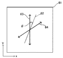
図8は本発明の第3の実施の形態例の画像表示装置の概念的な構成を示す図である。同図において、図1と同じ参照符号は同じ構成要素を示す。同図の(a)に示す画像表示装置60は、図1に示す第1の実施の形態例の画像表示装置10と異なる構成要素として1/2波長板61を設けている。1/4波長板14を出射した時点で直線偏光の電場の振動の方向はy軸に平行である。ここで第2の位相器である1/2波長板61の作用を図9に示すと、同図に示したxy座標(z軸は紙面に垂直方向)に対して1/2波長板61は図9のように配置されている。また、この1/2波長板61の遅相軸62を図9に示す。今、1/2波長板61に入射する直線偏光(1/4波長板出射後の)の電場の振動の方向は方向63であり、これと遅相軸62との成す角をθとする。入射する直線偏光の電場の振動の方向は1/2波長板61の作用によりθ回転させられ、1/2波長板61を出射するときには、入射時の直線偏光の電場の振動の方向からみると2θ回転している。この2θの角度でもって、空間光変調素子の画素に入射する。これ以降は第1の実施の形態例での説明と同様であり、画素数の増大効果が得られる。第1の実施の形態例においては、空間光変調素子の正方形状の画素配列と偏光ビームスプリッタとは、ねじれた位置関係にあったが(図6の(b)、(c)参照)、本実施の形態例においては、図10に示すように、偏光ビームスプリッタ71及び空間光変調素子の正方形状の画素の配列72とはねじれた位置関係にはなく、直線偏光の電場の振動の方向73がx(y)軸から傾いていることになる。この実施の形態例においては、従来の光学系に1/2波長板をその遅相軸を調整して設置するだけでよく、より低コスト化が図れる。
FIG. 8 is a diagram showing a conceptual configuration of an image display apparatus according to the third embodiment of the present invention. In the figure, the same reference numerals as those in FIG. 1 denote the same components. The
図11は本発明の第4の実施の形態例に係る画像表示装置の構成を示す図である。同図において、図5と同じ参照符号は同じ構成要素を示す。図11に示す第4の実施の形態例の画像表示装置80において、図5の第2の実施の形態例の画像表示装置30と異なる点は1/2波長板81を設けた点である。本実施の形態例でも、偏光分離素子にワイヤグリッド偏光子31を用いており、1/4波長板は省いている。ワイヤグリッド偏光子31を用いることにより高コントラスト比が可能となる。1/2波長板81の遅相軸と直線偏光の電場の振動の方向の、入射時に成す角度(図9におけるθ)を22.5°とし、出射時の角度(入射時の直線偏光の電場の振動方向からの)を45°とし、光偏向素子により光偏向の方向をx(y)軸からみて45°とするためのものである。これは、上述のようにx及びy軸からの偏向量が同じで最大の画素数増大の効果が得られる。また、スクリーン上での偏向量が画素ピッチの対角線の半分となるようになる。この効果は、x,y両方向に画素ピッチの半分を偏向した効果に近い。斜め一方向の偏向における最大の効果が得られ、より高精細な画像が可能となる。
FIG. 11 is a diagram showing the configuration of an image display apparatus according to the fourth embodiment of the present invention. In the figure, the same reference numerals as those in FIG. 5 denote the same components. The
次に、図12は色分離光学系の一例を示す概略図である。同図に示すように、色分離光学系の一例としては、回転軸95を中心に回転する赤、緑、赤のフィルタから成る円板を有するカラーホイール92である。光源91を出射した白色光94は、カラーホイール92により時分割で赤、青、緑の光の3原色に分離される。分離された3原色の各光96に対して、光偏向素子93は光偏向を行うが、高速な液晶のオフとオンとの切り換えが必要となる。3色のうち1色のみ光偏向をすることにより、光偏向素子93の切り換え速度が1/3に低減される。高速応答する液晶に、垂直配向型液晶があるが、液晶ディスプレイなどにおいても現状ではまだ使われていない。速度が1/3になれば、従来からのツイストネマチック液晶等でも対応でき、より低コスト化が図れる。ここで、光偏向する色を緑にするものである。これは、緑の光が観察者にとって比視感度が最大であり、他の2色よりも、光偏向した際に、画素数増大の効果が有利と考えられるためである。よって、図4の(c)において、光偏向により重ね合わされた画像には、画素間に重なりがあることが分かる。残像を用いているため、このままでも画素数増大の効果は得られる。しかし、図13の(a)に示すように画素を縮小してから、図13の(b)に示すように光偏向して重ね合わせると、さらに高精細な画像が得られる。このように画素を縮小する方法としては、空間光変調素子の画素配列に合わせてマイクロレンズアレイを設ける方法がある。
Next, FIG. 12 is a schematic diagram showing an example of a color separation optical system. As shown in the figure, an example of a color separation optical system is a color wheel 92 having a disk made of red, green, and red filters that rotate about a
その断面図を図14に示す。同図の(a)に示す反射型空間光変調素子100は、マイクロレンズアレイ101、樹脂(接着)層102、カバーガラス103、液晶層104、画素電極(画素)105、半導体基板106である。次に、図14の(b)に画素が縮小される原理を示す。入射する光107は、マイクロレンズ108により集光され、画素電極105で反射され、更にマイクロレンズ108により集光されて出射する。この過程において、光束が細くなる位置109が存在する。この位置109を投射レンズの物面とすれば、スクリーン上に図13の(a)に示した縮小した画素を投射することが可能となる。なお、ここでの位置109を光束が細くなる位置としたが、入射光は発散角を有し、また光源の配光分布もあるため、これからずれた位置を投射レンズの物面としたときに、適切な縮小画素が得られる場合もある。
A cross-sectional view thereof is shown in FIG. A reflective spatial
図15に示す反射型空間光変調素子110は、カバーガラス111、対となる透明電極112、114、液晶層113、半導体基板117、凹面状の反射画素116、凹面を充填する透明部材115を含んで構成されている。入射する光線は、凹面鏡により、集光される。画素を縮小する機能は図13に示すマイクロレンズの一例と同じであるが、凹面鏡を使うことに、色収差が低減でき、また曲率半径も大きくてよく、このため球面収差も低減でき、より高品位な画像を提供できる。
A reflective spatial
図16は本発明の第5の実施の形態例に係る画像表示装置の構成を示す図である。同図において、図1と同じ参照符号は同じ構成要素を示す。図16に示す第5の実施の形態例の画像表示装置120は、光源11、第1の偏光子121、光偏向素子15、反射型空間光変調素子16、第2の偏向子122、投射レンズ17を含んで構成されている。また、第1の偏光子121及び第2の偏光子122は所謂、偏光子と検光子である。光源11は上記各実施の形態例同様に白色ランプであり、無偏光光が出射される。
FIG. 16 is a diagram showing the configuration of an image display apparatus according to the fifth embodiment of the present invention. In the figure, the same reference numerals as those in FIG. 1 denote the same components. The
次に、図16に示す第5の実施の形態例における光学系の各素子また直線偏光の電場の振動方向の変化及び光路の偏向について、図17を用いて説明する。図17の(a)は第1の偏光子121であり、その透過軸121−1が、xyの座標(z軸は図面に対して垂直であり、この座標は図17の(b)、(c)、(d)においても共通とする)のy軸に平行である。図16の光源11からの光は、第1の偏光子121を透過した時点で、この透過軸の方向(y軸)と電場の振動方向が平行な直線偏光となっている。そして、図17の(b)は、光偏向素子15であり、その偏向方向を15−4(x軸と平行)とする。光偏向素子15は、この偏向方向15−4と平行な電場の振動方向の直線偏光がこの素子に入射したときには光路を偏向させることができ、一方偏向方向15−4と垂直な電場の振動方向の直線偏光が入射した場合には、上述したように、光路を偏向させ得ない。第1の偏光子121を透過した直線偏光の電場の振動方向は、光偏向素子15の偏向方向に対して垂直であるため、直線偏光は偏向されずに、光偏向素子を透過する。光偏向素子15を透過した後の、直線偏光の電場の振動方向はx軸に平行である。図17の(c)は図3と同様に反射型空間光変調素子16と、正方形状の画素配列を示している。正方形状の画素の辺の水平、垂直方向は、x軸、y軸の方向と一致している。画素に入射する直線偏光の電場の振動方向はy軸に平行、すなわち図17の(c)において方向16−1である。この直線偏光は、反射型空間光変調素子16の画素に入射し、反射画素電極で反射、光路を反転させて出射という過程を経る。この過程で、反射型空間光変調素子16の変調機能により、直線偏光の電場の振動方向を90°回転させて、図17の(c)の方向16−2の状態で、出射させる。また、変調させない場合は、入射時と変らない図17の(c)の方向16−1の状態で、出射される。反射型空間光変調素子16は画素毎にこの変調が可能であり、方向16−1、16−2のいずれかは、画素毎により異なり、またこれは表示させたい画像による。なお、ここでは1画素に関して説明している。図17の(d)は、第2の偏光子122であり、その透過軸122−1を有する。反射型空間光変調素子16を出射した直線偏光で電場の振動方向が方向16−2の場合、第2の偏光子122を透過し、図16の投射レンズ17を経て、スクリーン19に到達し、これが明状態(白表示)であり、一方電場の振動方向が方向16−1の場合、第2の偏光素子122を透過することができず、ここで吸収、反射され、スクリーン19に到達しない、これが暗状態(黒表示)である。
Next, changes in the vibration direction of the electric field of each optical system or linearly polarized electric field and optical path deflection in the fifth embodiment shown in FIG. 16 will be described with reference to FIG. 17A shows the
また、所定の電場の振動の方向と図16の第1の偏光子121の透過軸とが直交する配置である。所謂クロスニコルの配置であり、精度良く所定の電場の振動の直線偏光を取り出すことができる。更に、所定の電場の振動の方向と第1の偏光子121の透過軸が直交しない場合を図18に示す。このとき入射時に光偏向素子により偏向される場合があるが、画像の情報を持たないため、表示画像に問題はない。また、この場合第1の偏光子121と第2の偏光子122の透過軸が同じ方向であるため、この2つの偏光子を一体にした素子を用いても構わない。また、第1の偏光子121、122の偏向方向を90°回転させることにより、y軸方向のシフトも可能となる。
In addition, the vibration direction of the predetermined electric field and the transmission axis of the
次に、光偏向素子による画素数増大の効果を図19に示す。図19の(a)は画素を全部白表示させた場合を示している。上述したように、光偏向素子の偏向方向をx軸に平行として、図19の(a)の全白表を、偏向させた場合、図19の(b)のように、0の位置からx軸方向にずれた位置に、表示がずれる。このとき、光偏向素子の透明ガラスの屈折率、厚み、液晶の種類、また液晶の印加電圧の大小により、ずれる量がスクリーン上での1画素の半分の大きさになるように、偏向量を調節する。この図19の(a)、(b)の切り換えを高速で行うことにより、見かけ上、画素数が2倍に増大し、つまり2倍に増大して見える。見かけ上とは、観察者の残像によるためである。この表示の切り換えの速度は観察者がフリッカを感じない60Hz以上が好ましい。また光偏向素子に用いる液晶材料としては、高速な切り換えが可能な垂直配向型の液晶が好ましい。
Next, the effect of increasing the number of pixels by the optical deflection element is shown in FIG. FIG. 19A shows a case where all pixels are displayed in white. As described above, when the deflection direction of the optical deflecting element is parallel to the x-axis and the entire white table of FIG. 19A is deflected, the x position is shifted from the
次に、図16に示す第5の実施の形態例における光学系の各素子また直線偏光の電場の振動方向の別の変化及び別の光路の偏向について、図20を用いて説明する。図20の(a)は第1の偏光子121であり、その透過軸121−1が、xyの座標(z軸は図面に対して垂直であり、光路と一致し、またこの座標は図20の(b)、(c)、(d)においても共通とする)に対して、z軸を中心に回転している。光源からの光は、第1の偏光子121を透過した時点で、この透過軸の方向と電場の振動方向が平行な直線偏光になっている。次に、図20の(b)は、光偏向素子15を示しており、その偏向方向を15−4とする。この方向に平行な電場の振動方向の直線偏光がこの素子に入射したときに、光軸(z軸)に沿ってこの方向に光が偏向する。また、この方向と直交する電場の振動方向の直線偏光が入射したときには、光は偏向しない。ここで、第1の偏光子121を透過した直線偏光の電場の振動方向は方向121−1と平行であり、これは光偏向素子15の偏向方向15−4と直交するため、光は偏向されずに、光偏向素子15を透過する。図20の(c)は反射型空間光変調素子16を示したものであり、正方形状の画素が配列している。このとき正方形状の画素の辺の水平、垂直方向はxy座標と一致している。また、この正方形状の画素に入射する直線偏光の電場の振動方向は、この水平、垂直方向と一致していない。この説明において、入射する直線偏光の電場の振動方向は図20の(a)で示した方向121−1であった。反射型空間光変調素子16の変調機能により、入射した直線偏光の電場の振動方向は、図20の(c)において、入射時と変らない方向16−1、あるいは入射時から90度回転した方向16−2の2つのいずれかを取る。図20の(d)は、第2の偏光子(検光子)122を示しており、透過軸122−1を有し、これは図20の(a)の第1の偏光子121の透過軸121−1とは直交している。反射型空間光変調素子16を出射した直線偏光は、図20の(c)において、その電場の振動方向が方向16−2の場合、光偏向素子15及び第2の偏光子122を透過して(偏光子の透過軸と直線偏光の電場の振動方向が一致するため)、図16の投射レンズ17を経て、スクリーンに到達する。これが明状態である。また光偏向素子15の偏向機能により、光路が偏向され得る。一方、反射型空間光変調素子16を出射した直線偏光の電場の振動方向が方向16−1の場合、光偏向素子15を透過した後、検光子で、その透過軸と偏向方向が直交するため、検光子により吸収、反射され、投射レンズ17、スクリーンには到達しない。これが暗状態である。このように、図17ではxあるいはy軸方向の偏向であったが、図20では斜め方向の偏向が可能となる。また、光偏向素子の配置に関して図2におけるx軸(あるいはy軸)は図20の(b)における光偏向素子15の偏向方向15−4と一致しているものとする。なお、斜め方向の光偏向による画素数増加の効果については上述した図4によって説明しているのでここでは省略する。
Next, another change in the vibration direction of each element of the optical system or linearly polarized electric field and deflection of another optical path in the fifth embodiment shown in FIG. 16 will be described with reference to FIG. 20A shows the
また、光偏向させる方向を、空間光変調素子の正方形状の画素の対角方向(x軸あるいはy軸から45°)であるとしたものである。光偏向させる方向を45°でなく0°(水平)に近付けた場合、一方向の光偏向に近くなり、一方向しか画素数が向上しない。これに対して45°であれば、光偏向においては、x及びy軸ともに偏向量が同じであり、x、y方向の偏向を独立に行うのと近く、4倍の画素数増加に近い効果が得られると考えられる。また、正方形状の画素の対角方向であるため、45°と等価な135°、225°、315°方向の偏向であっても構わない。このとき、光学系の各構成要素は、その偏向方向に対応するように配置する。 In addition, the direction of light deflection is the diagonal direction of the square pixel of the spatial light modulator (45 ° from the x-axis or y-axis). When the light deflection direction is close to 0 ° (horizontal) instead of 45 °, it becomes close to light deflection in one direction, and the number of pixels is improved only in one direction. On the other hand, if the angle is 45 °, the amount of deflection in the x and y axes is the same in light deflection, and it is close to performing the deflection in the x and y directions independently, and an effect close to a four times increase in the number of pixels. Can be obtained. Further, since it is the diagonal direction of the square pixel, it may be deflected in the directions of 135 °, 225 °, and 315 ° equivalent to 45 °. At this time, each component of the optical system is arranged so as to correspond to the deflection direction.
図21は本発明の第6の実施の形態例に係る画像表示装置の構成を示す図である。同図において、図16と同じ参照符号は同じ構成要素を示す。図21に示す第6の実施の形態例の画像表示装置130は、光源11、第1の偏光子121、1/2波長板である位相器131、光偏向素子15、反射型空間光変調素子16、第2の偏向子122、投射レンズ17を含んで構成されている。
次に、図21に示す第6の実施の形態例における光学系の各素子また直線偏光の電場の振動方向の変化及び光路の偏向について、図22を用いて説明する。図22の(a)は、第1の偏光子121であり、透過軸121−1を有している。第1の偏光子121を透過した後の直線偏光の電場の振動方向はy軸と平行である。図22の(b)に示す位相器(1/2波長板)131は、遅相軸132を有している。1/2波長板に入射するときの直線偏光の電場の振動方向が方向133であり、1/2波長板を出射した後の直線偏光の電場の振動方向が方向134である。入射時の電場の振動方向133と遅相軸132との成す角をθとすると、入射時の電場の振動方向133と出射時の電場の振動方向134との成す角は2θである(1/2波長板の機能による)。図22の(c)は、光偏向素子15でありその光偏向方向が方向15−4である。1/2波長板を出射した直線偏光の電場の振動方向は方向134であり、光偏向方向15−4と直交するものとする。このとき光は偏向されない。図22の(d)は反射型空間光変調素子16とその正方形状の画素配列である。正方形状の画素の辺の水平、垂直方向とxy方向とは一致していない。反射型空間光変調素子16の画素に図22の(b)の方向134の電場の振動方向の直線偏光が入射すると、空間光変調素子15の変調機能により、直線偏光の電場の振動方向は図22の(d)の電場の振動方向16−1と電場の振動方向16−2との2つのうちいずれかとなる。このとき、電場の振動方向16−1と図22の(b)の方向134の方向は一致しているものとする。次に、図22の(d)の電場の振動方向16−1あるいは電場の振動方向16−2の電場の振動方向の直線偏光は、光偏向素子15を透過する。このとき、電場の振動方向16−2の直線偏光は、偏向され、電場の振動方向16−1の直線偏光は、偏向されない。次に、この2つの電場の振動方向の直線偏光は、1/2波長板である位相器131を通る。このとき、電場の振動方向が電場の振動方向16−1の直線偏光は、1/2波長板の機能により、電場の振動方向がy軸と平行な直線偏光となり、電場の振動方向が電場の振動方向16−2の直線偏光は、電場の振動方向がx軸と平行な直線偏光となる。図22の(e)は第2の偏光子122であり、その透過軸122−1でx軸に平行である。1/2波長板である位相器131を出射したx軸に平行な直線偏光は第2の偏光子122を透過、図21の投射レンズ17を経てスクリーン19へ到達(明状態)、一方1/2波長板である位相器131を出射したy軸に平行な直線偏光は第2の偏光子122により吸収、反射され、投射レンズ17、スクリーン19へは到達しない(暗状態)。
なお、1/2波長板である位相器131の遅相軸132と直線偏光の電場の振動の方向の、入射時に成す角度(図22の(b)におけるθ)を22.5°とし、出射時の角度(入射時の直線偏光の電場の振動方向からの)を45°とし、光偏向素子により光偏向の方向をx(y)軸からみて45°とするためのものである。これは、上述のようにx及びy軸からの偏向量が同じで最大の画素数増大の効果が得られる。また22.5°と等価な112.5°、202.5°、292.5°であっても構わない。
FIG. 21 is a diagram showing a configuration of an image display apparatus according to the sixth embodiment of the present invention. In the figure, the same reference numerals as those in FIG. 16 denote the same components. The
Next, changes in the vibration direction of the electric field of each optical system or linearly polarized electric field and deflection of the optical path in the sixth embodiment shown in FIG. 21 will be described with reference to FIG. FIG. 22A shows a
The angle (θ in FIG. 22B) between the
図23は本発明の第7の実施の形態例に係る画像表示装置の構成を示す図である。同図において、図16と同じ参照符号は同じ構成要素を示す。図23に示す第7の実施の形態例の画像表示装置140は、光偏向素子15を、空間光変調素子16と第2の偏光子122との光路(復路)にのみ設けるものである。本実施の形態例のようにすれば、光学系に余計な部材が入らず、それだけ消光比及びコントラスト比が向上するだけでなく、光偏向素子の大きさが、およそ半分の大きさですむため、さらに低コスト化が図れる。
FIG. 23 is a diagram showing the configuration of an image display apparatus according to the seventh embodiment of the present invention. In the figure, the same reference numerals as those in FIG. 16 denote the same components. In the
図24は本発明の第8の実施の形態例に係る画像表示装置の構成を示す図である。同図において、図21と同じ参照符号は同じ構成要素を示す。図24に示す第8の実施の形態例の画像表示装置150は、光偏向素子15を、反射型空間光変調素子16と位相器131との光路(復路)にのみ設けるものである。本実施の形態例のようにすれば、光学系に余計な部材が入らず、それだけ消光比及びコントラスト比が向上するだけでなく、光偏向素子の大きさが、およそ半分の大きさですむため、さらに低コスト化が図れる。
FIG. 24 is a diagram showing the configuration of an image display apparatus according to the eighth embodiment of the present invention. In the figure, the same reference numerals as those in FIG. 21 denote the same components. In the
図25は本発明の第9の実施の形態例に係る画像表示装置の構成を示す図である。同図において、図1と同じ参照符号は同じ構成要素を示す。図25に示す第9の実施の形態例の画像表示装置160は、光源11、偏光子12、偏光分離素子13、第1の光偏向素子161、位相器162、第2の光偏向素子163、反射型空間光変調素子16、投射レンズ17を含んで構成されている。このような構成を有する本実施の形態例の画像表示装置160によれば、光源11から出射した無偏光の白色光は、偏光子12により直線偏光(s偏光)にされ、当該s偏光が偏光分離素子13に入射される。そして偏光を分離する面18で反射され、偏光分離素子13を出射したs偏光は第1の光偏向素子161に入射し、偏向されずに出射し、位相器162に入射する。ここで、位相器162は1/2波長板であり、図9に示すように位相器162から出射する直線偏光は入射時から2θ、その電場の振動面が回転することなる。そして、第2の光偏向素子163は、その偏向面が出射する直線偏光の電場の振動面に対して垂直になるように設置され、よって位相器162を出射する直線偏光は第2の光偏向素子163に入射し、偏向されずに透過し、空間光変調素子16に入射する。そして、液晶により電場の振動面が変調されなかった直線偏光は、空間光変調素子16から出射後、第2の光偏向素子163に入射し、偏向されずに出射して、そして位相器162に入射する。この位相器162によりその電場の振動面を2θ、上記とは逆に回転させてs偏光となり、第1の光偏向素子161に入射する。第1の光偏向素子161の液晶の印加電圧によっては偏向されずに出射し、偏光分離素子13に入射する。そして、偏光分離素子13の偏光機能を有する面18で反射されて光源11へ戻る。このためスクリーン19に光が到達することは無く、よってスクリーン19上では暗(黒)表示となる。一方、液晶により電場の振動面が変調された直線偏光は、空間光変調素子16から出射後、第2の光偏向素子163に入射し、偏向されて出射して、そして位相器162に入射する。この位相器162によりその電場の振動面を2θ、上記とは逆に回転させてp偏光となり、第1の光偏向素子161に入射する。第1の光偏向素子161の液晶の印加電圧によっては偏向されて出射し、偏光分離素子13に入射する。そして、偏光分離素子13の偏光機能を有する面18を透過して投射レンズ17を経てスクリーン19に到達する。このためスクリーン19上では明(白)表示となる。
FIG. 25 is a diagram showing the configuration of an image display apparatus according to the ninth embodiment of the present invention. In the figure, the same reference numerals as those in FIG. 1 denote the same components. The
このように、直線偏光は、第1の光偏向素子161及び第2の光偏向素子162によって、液晶の印加電圧によって偏向される。2つの光偏向素子で偏向するとスクリーン19上では4つの異なる位置に光を到達させることができ、よって画素の像を投射させることができる。ここで明表示の9つの画素をスクリーンに投射した場合を一例にして説明すると、偏向されていないときの図26の(a)から、図26の(b)のように第2の光偏向素子により斜めに偏向されて偏向量はスクリーン上で画素ピッチの半分になる。または、図26の(c)のように第1の光偏向素子により横に偏向される。また、図26の(d)のように第2の光偏向素子により図26の(b)とは逆方向に斜めに偏向される。このように図26の(a)から図26の(d)までの一連の偏向を観察者がフリッカを感じない60Hz以上の高速で行えば、観察者は滑らかな画像を見ていると感じる。特に斜め線の画像を表示させたときに目立つジャギィの低減に効果がある。また、この場合の画素数において4倍増に相当する画像が期待できる。
Thus, the linearly polarized light is deflected by the applied voltage of the liquid crystal by the first
図27は第1、第2の偏向素子及び空間光変調素子の印加電圧の波形を示すタイミングチャートである。ここでは第1の光偏向素子は斜め方向の偏向、第2の光偏向素子は水平(左右)方向の偏向とする。2つの光偏向素子により、(斜め下、左)、(斜め上、左)、(斜め上、右)、(斜め上、右)の4つの異なる偏向が可能となる。この間に空間光変調素子は4回点滅する。図27の(c)に示すように、これが1フィールドであり、すなわち4サブフィールドから成る。これは4サブフィールド駆動と呼ばれる。また、これをスクリーン上に投射した1画素として表現したものが図28であり、周辺の画素をあわせて描くと図26のようになる。なお、図27において、2つの光偏向素子の印加電圧を矩形波に、空間光変調素子の印加電圧をδ関数的に表現しているが適宜的なものでこれに限定するものではない。 FIG. 27 is a timing chart showing waveforms of voltages applied to the first and second deflection elements and the spatial light modulation element. Here, it is assumed that the first light deflecting element is deflected in an oblique direction, and the second light deflecting element is deflected in a horizontal (left / right) direction. With the two light deflection elements, four different deflections are possible: (diagonally lower, left), (diagonally upper, left), (diagonally upper, right), (diagonally upper, right). During this time, the spatial light modulator flashes four times. As shown in FIG. 27C, this is one field, that is, four subfields. This is called 4-subfield driving. FIG. 28 represents this as one pixel projected on the screen, and FIG. 26 shows the surrounding pixels together. In FIG. 27, the applied voltage of the two light deflection elements is expressed as a rectangular wave, and the applied voltage of the spatial light modulation element is expressed as a δ function, but it is appropriate and not limited to this.
更に、図29は第1、第2の偏向素子及び空間光変調素子の印加電圧の別の波形を示すタイミングチャートである。同図は3サブフィールド駆動と呼ばれている。図27では、斜め上と斜め下の偏向、また右と左の偏向の電圧印加時間を等しくする駆動であったが、図29ではこれらを等しくしない駆動である。つまり図30に示すように、斜め方向の偏向は左にあるときのみ行う。このような偏向によってもスクリーン上を投射画素により隙間無く埋めることができ、画素の形状は三角形になるが、画素の高精細化が図れる。また、この3サブフィールド駆動によりだい1、第2の光偏向素子及び空間光変調素子の駆動周波数を4サブフィールド駆動の3/4に下げることができる。このため、より反応の遅い、従来の安価な液晶材料を用いることができ、低コスト化が図れ、また駆動周波数を下げることにより負荷が低減して耐久性が向上する。また、斜め方向の角度及び偏向の大きさを変えることにより、図30の(d)のように三角形の近い偏向も可能となる。 Further, FIG. 29 is a timing chart showing another waveform of the voltage applied to the first and second deflection elements and the spatial light modulation element. This figure is called three-subfield driving. In FIG. 27, the driving is performed such that the voltage application times of the diagonally upper and lower deflections, and the right and left deflections are equalized, but in FIG. 29, these are not equalized. That is, as shown in FIG. 30, the oblique deflection is performed only when it is on the left. Even with such deflection, the screen can be filled with projection pixels without gaps, and the shape of the pixels becomes a triangle, but high definition of the pixels can be achieved. In addition, the driving frequency of the first and second light deflection elements and the spatial light modulation element can be reduced to 3/4 of the four subfield driving by the three subfield driving. For this reason, it is possible to use a conventional inexpensive liquid crystal material that is slower in reaction, and the cost can be reduced, and the load is reduced and the durability is improved by lowering the driving frequency. Further, by changing the angle in the oblique direction and the magnitude of the deflection, it becomes possible to deflect the triangle as close as shown in FIG.
図31は本発明の第10の実施の形態例に係る画像表示装置の構成を示す図である。同図において、図25と同じ参照符号は同じ構成要素を示す。1/2波長板である位相器162は、第1の光偏向素子161と第2の光偏向素子163の間にあればよく図31のような配置も可能である。図31に示す第10の実施の形態例の画像表示装置170では、光偏光分離素子13が第2の光偏向素子163と、位相器162及び第1の光偏向素子161との間にある構成であるが、上述したように1/2波長板である位相器162は、第1の光偏向素子161と第2の光偏向素子163との間に配置されている。第9の実施の形態例と同様に、画像の高精細化の効果が得られる。
FIG. 31 is a diagram showing a configuration of an image display apparatus according to the tenth embodiment of the present invention. In the figure, the same reference numerals as those in FIG. 25 denote the same components. The
図32は空間光変調素子を光軸に回転させた配置にした様子を示す図である。図25及び図31に示す画像表示装置において反射型空間光変調素子のみを回転させ、この回転角を2θとする。この場合、画素に入射する直線偏光の電場の振動面が画素の辺と平行(又は垂直)となる。これは従来技術における画素の位置と入射する直線偏光との関係である。このため、従来の反射型空間光変調素子を、ラビング層等を変えることなく用いることができる。また、スクリーン上での画像は、図33のように、x,y軸から斜めになって投射されるようになる。しかし、これは装置全体を回転させる機構を持たせれば問題ない。なお、図33は1つの画素のみを示している。 FIG. 32 is a diagram showing a state in which the spatial light modulator is arranged around the optical axis. In the image display device shown in FIGS. 25 and 31, only the reflective spatial light modulator is rotated, and the rotation angle is 2θ. In this case, the vibration plane of the linearly polarized electric field incident on the pixel is parallel (or perpendicular) to the side of the pixel. This is the relationship between the position of the pixel and the incident linearly polarized light in the prior art. For this reason, the conventional reflective spatial light modulator can be used without changing the rubbing layer or the like. The image on the screen is projected obliquely from the x and y axes as shown in FIG. However, this is not a problem if a mechanism for rotating the entire apparatus is provided. FIG. 33 shows only one pixel.
図34は本発明の第11の実施の形態例に係る画像表示装置の構成を示す図である。同図において、図25と同じ参照符号は同じ構成要素を示す。同図に示す本実施の形態例の画像表示装置180は、偏光分離素子にワイヤグリッド偏光子(グリッド偏光子)181を用いた構成である。ワイヤグリッド偏光子181は、複屈折偏光子や2色性を利用した偏光子よりも、消光比を高くすることが可能である。
FIG. 34 is a diagram showing a configuration of an image display apparatus according to the eleventh embodiment of the present invention. In the figure, the same reference numerals as those in FIG. 25 denote the same components. The
図35は本発明の第12の実施の形態例に係る画像表示装置の構成を示す図である。同図において、図25と同じ参照符号は同じ構成要素を示す。同図に示す第12の実施の形態例の画像表示装置190は、光源11、第1の偏光子191、1/2波長板である位相器162、第1の光偏向素子161、反射型空間光変調素子16、第2の光偏向素子163、第2の偏光子192を含んで構成されている。第2の偏光子192は所謂検光子であり、第2の偏光子192の透過軸は第1の偏光子191の透過軸と直交している(クロスニコル)。この光学系はオフアクシス(Off-Axis)である。このような構成を有する第12の実施の形態例の画像表示装置によれば、光源11から無偏光の光が放射され、第1の偏光子191を透過したときは直線偏光となる。このとき、直線偏光の電場の振動面をy軸に平行とする。次に1/2波長板である位相器162の遅相軸はy軸からz軸周りに回転した位置にあり、x軸,y軸のどちらとも一致しないものとする。1/2波長板である位相器162に入射する直線偏光は、y軸から2θ回転した電場の振動面を有する直線偏光となり、第1の光偏向素子161を透過して、反射型空間光変調素子16に入射する。画素で反射された直線偏光が反射型空間光変調素子16で変調されない場合、第1の光偏向素子161を透過して位相器162で上記とは逆に2θ、電場の振動面を回転して、y軸に平行な直線偏光となる。そして、第2の光偏光素子163を透過し、第2の偏光子192で反射及び吸収される。この第2の偏光子192の透過軸の方向は、x軸に平行であり、電場の振動面がy軸に平行な直線偏光は透過できない。このときスクリーン上に光は到達できず、暗表示(黒表示)となる。一方、空間光変調素子16で電場の振動面が変調された直線偏光は、その電場の振動面が図9の方向64に対して垂直となる。この直線偏光は、第1の光偏向素子161を透過し、位相器162で上記と逆に2θ回転して、x軸に電場の振動面が平行な直線偏光となる。この直線偏光は、第2の光偏向素子163を透過した後、第2の偏光子192を透過してスクリーン19に到達し、明表示(黒表示)となる。また、この行程において、第1の光偏向素子161及び第2の光偏向素子163で偏向が可能となり、これを全て偏向した場合、上述したような4サブフィールド駆動、つまりスクリーン19上で4つの異なる位置をとり得られる。このため、見かけ上の画素数の増大による画質の向上が達成される。また、上述した3サブフィールド駆動も可能である。更に、このようなオフアクシスの光学系においては偏光子と検光子が用いられ、従来の偏光子を用いるため低コストとなる。また、この偏光子と検光子の構成においては、高い消光比が得られ、高コントラスト比が達成できる。また、1/2波長板である位相器162の遅相軸と、この位相器162に入射する直線偏光の電場の振動面との成す角を22.5°とするとき、正方形の画素の辺と、入射する直線偏光の電場の振動面との成す角は45°となり、これは正方形の対角線となって対角線上の光偏向となる。また、画素ピッチの対角線の半分に相当する距離にシフトさせれば、画素数を増大でき、高コントラストとなり、かつより高精細な画像が表示できる。
FIG. 35 is a diagram showing the configuration of an image display apparatus according to the twelfth embodiment of the present invention. In the figure, the same reference numerals as those in FIG. 25 denote the same components. The
また、図36は画素縮小を行い、斜め一方向と横方向の両偏向を行った場合の投射画素の様子を示す図である。同図に示すように、斜め一方向と横方向の両偏向を行うと、隙間無く画素の像を投射することが可能となり、実質4倍の画素数の増大となり、画素の縮小を1/2程度にしたときはさらに高精細な画像となる。 FIG. 36 is a diagram showing a state of a projection pixel when pixel reduction is performed and both deflection in one oblique direction and one lateral direction are performed. As shown in the figure, when both the oblique and lateral deflections are performed, it is possible to project a pixel image without a gap, which substantially increases the number of pixels by four times, and reduces the reduction of the pixels by 1/2. When it is set to about the level, a higher definition image is obtained.
なお、本発明は上記実施の形態例に限定されるものではなく、特許請求の範囲内の記載であれば多種の変形や置換可能であることは言うまでもない。 The present invention is not limited to the above-described embodiments, and it goes without saying that various modifications and substitutions are possible as long as they are described within the scope of the claims.
10;画像表示装置、11;光源、12;偏光子、
13;偏光分離素子、14;1/4波長板、15;光偏向素子、
16;空間光変調素子、17;投射レンズ、18;面、
19;スクリーン。
10; Image display device, 11; Light source, 12; Polarizer,
13; polarization separation element; 14; quarter wave plate; 15; light deflection element;
16; spatial light modulation element, 17; projection lens, 18; surface,
19; Screen.
Claims (12)
前記光源から前記偏光分離素子に入射した直線偏光が、前記偏光分離素子の偏光分離機能を有する面で反射されて前記偏光分離素子から出射し、その偏光分離素子から出射した直線偏光が偏向されずに前記光偏向素子を透過して前記反射型空間光変調素子に入射し、前記反射型空間光変調素子の各画素で反射された直線偏光が、前記反射型空間光変調素子への入射時とは逆方向から前記光偏向素子に入射し、前記光偏向素子と前記偏光分離素子の偏光分離機能を有する面とを透過し前記投射レンズを経て出射するように、前記光源、前記偏光分離素子、前記光偏向素子、前記反射型空間光変調素子及び前記投射レンズが配置され、
前記偏光分離素子は、前記偏向分離機能を有する面が、前記光源からの直線偏光の電場の振動の方向に対して平行であり、前記光源からの直線偏光を前記反射型空間光変調素子に向けて反射させ、前記光偏向素子を通過してきた直線偏光を前記投射レンズ側に通過させるように、設けられ、
前記反射型空間光変調素子は、前記光偏向素子を透過して入射してきた直線偏光の電場の振動の方向に対して、前記正方形状の画素の互いに直交する2辺それぞれに沿った2方向が一致しないように設けられ、
前記光偏向素子は、前記偏光分離素子からの直線偏光を偏向しないで前記反射型空間光変調素子側に通過させ、前記反射型空間光変調素子で変調されて反射した直線偏光を、その直線偏光の入射方向と該直線偏光の電場の振動の方向とに対して平行な面内で、印加電圧に応じて光路を偏向して前記偏光分離素子側に通過させるように設けられていることを特徴とする画像表示装置。 A polarization separation element including a light source, a surface having a polarization separation function that separates two linearly polarized lights having different directions of vibration of the electric field, and linearly polarized light when linearly polarized light having a predetermined direction of vibration of the electric field is incident And a plurality of square-shaped pixels that can be modulated so that the direction of vibration of the electric field when incident linearly polarized light is reflected is rotated by 90 degrees. A reflective spatial light modulator arranged in two directions along each of the projection spatial light modulator, and a projection lens;
The linearly polarized light incident on the polarization separation element from the light source is reflected by the surface having the polarization separation function of the polarization separation element and emitted from the polarization separation element, and the linearly polarized light emitted from the polarization separation element is not deflected. The linearly polarized light reflected by each pixel of the reflective spatial light modulator is transmitted through the light deflecting element and incident on the reflective spatial light modulator. Is incident on the light deflection element from the reverse direction, passes through the light deflection element and the surface having the polarization separation function of the polarization separation element, and exits through the projection lens, the light source, the polarization separation element, The light deflection element, the reflective spatial light modulation element and the projection lens are arranged,
The polarization separation element has a plane having the deflection separation function parallel to the direction of vibration of the linearly polarized electric field from the light source, and directs the linearly polarized light from the light source toward the reflective spatial light modulation element. The linearly polarized light that has been reflected and passed through the light deflection element is provided to pass to the projection lens side,
The reflective spatial light modulation element has two directions along two orthogonal sides of the square pixel with respect to the direction of vibration of the linearly polarized electric field transmitted through the light deflection element. Provided not to match,
The light deflection element passes the linearly polarized light from the polarization separation element without deflecting to the reflective spatial light modulation element side, and modulates and reflects the linearly polarized light that is modulated by the reflective spatial light modulation element. In the plane parallel to the direction of incidence of the linearly polarized electric field and the direction of vibration of the electric field of the linearly polarized light, the optical path is deflected according to the applied voltage so as to pass through to the polarization separation element side. An image display device.
前記光源からの光が、前記第1の偏光子を経て前記光偏向素子を透過し、前記反射型空間光変調素子に入射し、前記反射型空間光変調素子の各画素で反射された直線偏光が、前記光偏向素子と前記第2の偏光子とを透過し前記投射レンズを経て出射するように、前記光源、前記第1の偏光子、前記光偏向素子、前記反射型空間光変調素子、前記第2の偏光子及び前記投射レンズが配置され、
前記第1の偏光子は、その第1の偏光子が有する透過軸の方向に対して電場の振動方向が平行な振動方向の直線偏光を透過させ、
前記反射型空間光変調素子は、前記第1の偏光子及び前記光偏向素子を透過して入射してきた直線偏光の電場の振動方向に対して、前記正方形状の画素の互いに直交する2辺それぞれに沿った2方向が一致しないように設けられ、
前記光偏向素子は、前記第1の偏光子からの直線偏光を偏向しないで前記反射型空間光変調素子側に通過させ、前記反射型空間光変調素子で変調されて反射した直線偏光を、その直線偏光の入射方向と該直線偏光の電場の振動の方向とに対して平行な面内で、印加電圧に応じて光路を偏向して前記第2の偏光子側に通過させるように設けられ、
前記第2の偏光子は、その第2の偏光子が有する透過軸が前記光偏向素子を通過した直線偏光の電場の振動方向と平行となるように設けられていることを特徴とする画像表示装置。 A light source, a first polarizer, an optical deflection element capable of controlling the deflection of linearly polarized light when the direction of vibration of the electric field is incident, and an electric field when the incident linearly polarized light is reflected A reflective spatial light modulation element in which a plurality of square-shaped pixels that can be modulated so as to rotate the direction of vibration of 90 degrees are arranged in two directions along two mutually orthogonal sides of the pixel; Having at least a polarizer and a projection lens;
Light from the light source passes through the first polarizer, passes through the light deflecting element, enters the reflective spatial light modulator, and is reflected by each pixel of the reflective spatial light modulator. The light source, the first polarizer, the light deflection element, the reflective spatial light modulation element, so as to pass through the light deflection element and the second polarizer and exit through the projection lens, The second polarizer and the projection lens are disposed;
The first polarizer transmits linearly polarized light having a vibration direction in which the vibration direction of the electric field is parallel to the direction of the transmission axis of the first polarizer,
The reflective spatial light modulation element includes two sides of the square pixel that are orthogonal to each other with respect to the vibration direction of the electric field of linearly polarized light that has been transmitted through the first polarizer and the light deflection element. Are provided so that the two directions along
The light deflection element passes the linearly polarized light from the first polarizer to the reflective spatial light modulation element without deflecting the linearly polarized light, and modulates and reflects the linearly polarized light that is modulated by the reflective spatial light modulation element. In a plane parallel to the incident direction of the linearly polarized light and the direction of vibration of the electric field of the linearly polarized light, the optical path is deflected according to the applied voltage and passed to the second polarizer side,
The second polarizer is provided so that a transmission axis of the second polarizer is parallel to a vibration direction of an electric field of linearly polarized light that has passed through the light deflecting element. apparatus.
Priority Applications (1)
| Application Number | Priority Date | Filing Date | Title |
|---|---|---|---|
| JP2004371140A JP4892188B2 (en) | 2004-12-22 | 2004-12-22 | Image display device |
Applications Claiming Priority (1)
| Application Number | Priority Date | Filing Date | Title |
|---|---|---|---|
| JP2004371140A JP4892188B2 (en) | 2004-12-22 | 2004-12-22 | Image display device |
Publications (2)
| Publication Number | Publication Date |
|---|---|
| JP2006178174A JP2006178174A (en) | 2006-07-06 |
| JP4892188B2 true JP4892188B2 (en) | 2012-03-07 |
Family
ID=36732348
Family Applications (1)
| Application Number | Title | Priority Date | Filing Date |
|---|---|---|---|
| JP2004371140A Expired - Fee Related JP4892188B2 (en) | 2004-12-22 | 2004-12-22 | Image display device |
Country Status (1)
| Country | Link |
|---|---|
| JP (1) | JP4892188B2 (en) |
Cited By (1)
| Publication number | Priority date | Publication date | Assignee | Title |
|---|---|---|---|---|
| CN109147469A (en) * | 2018-07-09 | 2019-01-04 | 安徽慧视金瞳科技有限公司 | A kind of calligraphy exercising method |
Families Citing this family (1)
| Publication number | Priority date | Publication date | Assignee | Title |
|---|---|---|---|---|
| JP6819759B2 (en) * | 2019-10-01 | 2021-01-27 | ソニー株式会社 | Light source device and image projection device |
Family Cites Families (6)
| Publication number | Priority date | Publication date | Assignee | Title |
|---|---|---|---|---|
| JP2002268014A (en) * | 2001-03-13 | 2002-09-18 | Olympus Optical Co Ltd | Image display device |
| JP4707270B2 (en) * | 2001-06-27 | 2011-06-22 | 株式会社リコー | Image projection device |
| JP2003186015A (en) * | 2001-12-20 | 2003-07-03 | Victor Co Of Japan Ltd | Liquid crystal display device |
| JP4057320B2 (en) * | 2002-03-22 | 2008-03-05 | 株式会社リコー | Optical path deflecting device and image display device |
| JP4537664B2 (en) * | 2002-04-17 | 2010-09-01 | 株式会社リコー | Optical path deflecting element, optical path deflecting device, image display device, optical writing device, optical interconnection device, optical element and manufacturing method thereof |
| US6805445B2 (en) * | 2002-06-05 | 2004-10-19 | Eastman Kodak Company | Projection display using a wire grid polarization beamsplitter with compensator |
-
2004
- 2004-12-22 JP JP2004371140A patent/JP4892188B2/en not_active Expired - Fee Related
Cited By (1)
| Publication number | Priority date | Publication date | Assignee | Title |
|---|---|---|---|---|
| CN109147469A (en) * | 2018-07-09 | 2019-01-04 | 安徽慧视金瞳科技有限公司 | A kind of calligraphy exercising method |
Also Published As
| Publication number | Publication date |
|---|---|
| JP2006178174A (en) | 2006-07-06 |
Similar Documents
| Publication | Publication Date | Title |
|---|---|---|
| JP4059066B2 (en) | projector | |
| JP4661510B2 (en) | Projection display device and three-plate liquid crystal projector | |
| WO2007052402A1 (en) | Polarization switching liquid crystal element, and image display comprising same | |
| KR100478804B1 (en) | Optical shifter and optical display system | |
| JP4133460B2 (en) | Projection-type image display device | |
| JP4052803B2 (en) | Image display device | |
| US8162485B2 (en) | Intermediate image formation optical system, image formation device, and methods thereof | |
| US7106389B2 (en) | Optical shifter and projection type optical display system | |
| JP6107006B2 (en) | projector | |
| JP2003207747A (en) | Image display optical unit, image display, and image display method | |
| JP2008139700A (en) | Image display device | |
| US7834941B2 (en) | Image display device | |
| JP4892188B2 (en) | Image display device | |
| KR20080075211A (en) | Birefringent Compensation Liquid Crystal Display and Projection System Using the Same | |
| JP2012208216A (en) | Projection type display device | |
| JP2003005132A (en) | Image projection device | |
| JP2001255605A (en) | projector | |
| JP4147902B2 (en) | projector | |
| JP3973524B2 (en) | Image shift element and image display device | |
| JP2015145934A (en) | projector | |
| JP2004004502A (en) | Optical apparatus and display apparatus | |
| JP2006293341A (en) | Image display device | |
| JP4075297B2 (en) | Projection display | |
| JP2002357809A (en) | Picture display device | |
| JP2002350780A (en) | Display device and picture projecting device |
Legal Events
| Date | Code | Title | Description |
|---|---|---|---|
| A621 | Written request for application examination |
Free format text: JAPANESE INTERMEDIATE CODE: A621 Effective date: 20071213 |
|
| RD02 | Notification of acceptance of power of attorney |
Free format text: JAPANESE INTERMEDIATE CODE: A7422 Effective date: 20091207 |
|
| RD04 | Notification of resignation of power of attorney |
Free format text: JAPANESE INTERMEDIATE CODE: A7424 Effective date: 20100115 |
|
| A977 | Report on retrieval |
Free format text: JAPANESE INTERMEDIATE CODE: A971007 Effective date: 20110331 |
|
| A131 | Notification of reasons for refusal |
Free format text: JAPANESE INTERMEDIATE CODE: A131 Effective date: 20110506 |
|
| A521 | Written amendment |
Free format text: JAPANESE INTERMEDIATE CODE: A523 Effective date: 20110704 |
|
| A131 | Notification of reasons for refusal |
Free format text: JAPANESE INTERMEDIATE CODE: A131 Effective date: 20110819 |
|
| A521 | Written amendment |
Free format text: JAPANESE INTERMEDIATE CODE: A523 Effective date: 20111017 |
|
| TRDD | Decision of grant or rejection written | ||
| A01 | Written decision to grant a patent or to grant a registration (utility model) |
Free format text: JAPANESE INTERMEDIATE CODE: A01 Effective date: 20111209 |
|
| A01 | Written decision to grant a patent or to grant a registration (utility model) |
Free format text: JAPANESE INTERMEDIATE CODE: A01 |
|
| A61 | First payment of annual fees (during grant procedure) |
Free format text: JAPANESE INTERMEDIATE CODE: A61 Effective date: 20111219 |
|
| R150 | Certificate of patent or registration of utility model |
Free format text: JAPANESE INTERMEDIATE CODE: R150 |
|
| FPAY | Renewal fee payment (event date is renewal date of database) |
Free format text: PAYMENT UNTIL: 20141222 Year of fee payment: 3 |
|
| LAPS | Cancellation because of no payment of annual fees |