JP4889205B2 - Active matrix display device - Google Patents
Active matrix display device Download PDFInfo
- Publication number
- JP4889205B2 JP4889205B2 JP2004195030A JP2004195030A JP4889205B2 JP 4889205 B2 JP4889205 B2 JP 4889205B2 JP 2004195030 A JP2004195030 A JP 2004195030A JP 2004195030 A JP2004195030 A JP 2004195030A JP 4889205 B2 JP4889205 B2 JP 4889205B2
- Authority
- JP
- Japan
- Prior art keywords
- voltage
- data line
- line
- current
- data
- Prior art date
- Legal status (The legal status is an assumption and is not a legal conclusion. Google has not performed a legal analysis and makes no representation as to the accuracy of the status listed.)
- Expired - Lifetime
Links
- 239000011159 matrix material Substances 0.000 title claims description 25
- 238000006243 chemical reaction Methods 0.000 claims description 75
- 239000003990 capacitor Substances 0.000 claims description 41
- 239000010409 thin film Substances 0.000 claims description 5
- 238000000034 method Methods 0.000 description 21
- 229910021420 polycrystalline silicon Inorganic materials 0.000 description 13
- 229920005591 polysilicon Polymers 0.000 description 13
- 239000000872 buffer Substances 0.000 description 12
- 238000010586 diagram Methods 0.000 description 12
- 230000001276 controlling effect Effects 0.000 description 9
- 238000012937 correction Methods 0.000 description 8
- 230000003213 activating effect Effects 0.000 description 6
- 229910021417 amorphous silicon Inorganic materials 0.000 description 5
- 239000000758 substrate Substances 0.000 description 5
- 239000011521 glass Substances 0.000 description 3
- 230000007423 decrease Effects 0.000 description 2
- 230000000694 effects Effects 0.000 description 2
- 239000004973 liquid crystal related substance Substances 0.000 description 2
- 239000002184 metal Substances 0.000 description 2
- 238000004904 shortening Methods 0.000 description 2
- XUIMIQQOPSSXEZ-UHFFFAOYSA-N Silicon Chemical compound [Si] XUIMIQQOPSSXEZ-UHFFFAOYSA-N 0.000 description 1
- 238000013459 approach Methods 0.000 description 1
- 238000005401 electroluminescence Methods 0.000 description 1
- 239000010408 film Substances 0.000 description 1
- 230000014759 maintenance of location Effects 0.000 description 1
- 238000012986 modification Methods 0.000 description 1
- 230000004048 modification Effects 0.000 description 1
- 230000036278 prepulse Effects 0.000 description 1
- 238000012545 processing Methods 0.000 description 1
- 230000001105 regulatory effect Effects 0.000 description 1
- 239000004065 semiconductor Substances 0.000 description 1
- 229910052710 silicon Inorganic materials 0.000 description 1
- 239000010703 silicon Substances 0.000 description 1
- 238000012546 transfer Methods 0.000 description 1
Images


Classifications
-
- G—PHYSICS
- G09—EDUCATION; CRYPTOGRAPHY; DISPLAY; ADVERTISING; SEALS
- G09G—ARRANGEMENTS OR CIRCUITS FOR CONTROL OF INDICATING DEVICES USING STATIC MEANS TO PRESENT VARIABLE INFORMATION
- G09G3/00—Control arrangements or circuits, of interest only in connection with visual indicators other than cathode-ray tubes
- G09G3/20—Control arrangements or circuits, of interest only in connection with visual indicators other than cathode-ray tubes for presentation of an assembly of a number of characters, e.g. a page, by composing the assembly by combination of individual elements arranged in a matrix no fixed position being assigned to or needed to be assigned to the individual characters or partial characters
- G09G3/22—Control arrangements or circuits, of interest only in connection with visual indicators other than cathode-ray tubes for presentation of an assembly of a number of characters, e.g. a page, by composing the assembly by combination of individual elements arranged in a matrix no fixed position being assigned to or needed to be assigned to the individual characters or partial characters using controlled light sources
- G09G3/30—Control arrangements or circuits, of interest only in connection with visual indicators other than cathode-ray tubes for presentation of an assembly of a number of characters, e.g. a page, by composing the assembly by combination of individual elements arranged in a matrix no fixed position being assigned to or needed to be assigned to the individual characters or partial characters using controlled light sources using electroluminescent panels
- G09G3/32—Control arrangements or circuits, of interest only in connection with visual indicators other than cathode-ray tubes for presentation of an assembly of a number of characters, e.g. a page, by composing the assembly by combination of individual elements arranged in a matrix no fixed position being assigned to or needed to be assigned to the individual characters or partial characters using controlled light sources using electroluminescent panels semiconductive, e.g. using light-emitting diodes [LED]
- G09G3/3208—Control arrangements or circuits, of interest only in connection with visual indicators other than cathode-ray tubes for presentation of an assembly of a number of characters, e.g. a page, by composing the assembly by combination of individual elements arranged in a matrix no fixed position being assigned to or needed to be assigned to the individual characters or partial characters using controlled light sources using electroluminescent panels semiconductive, e.g. using light-emitting diodes [LED] organic, e.g. using organic light-emitting diodes [OLED]
- G09G3/3225—Control arrangements or circuits, of interest only in connection with visual indicators other than cathode-ray tubes for presentation of an assembly of a number of characters, e.g. a page, by composing the assembly by combination of individual elements arranged in a matrix no fixed position being assigned to or needed to be assigned to the individual characters or partial characters using controlled light sources using electroluminescent panels semiconductive, e.g. using light-emitting diodes [LED] organic, e.g. using organic light-emitting diodes [OLED] using an active matrix
- G09G3/3233—Control arrangements or circuits, of interest only in connection with visual indicators other than cathode-ray tubes for presentation of an assembly of a number of characters, e.g. a page, by composing the assembly by combination of individual elements arranged in a matrix no fixed position being assigned to or needed to be assigned to the individual characters or partial characters using controlled light sources using electroluminescent panels semiconductive, e.g. using light-emitting diodes [LED] organic, e.g. using organic light-emitting diodes [OLED] using an active matrix with pixel circuitry controlling the current through the light-emitting element
- G09G3/3241—Control arrangements or circuits, of interest only in connection with visual indicators other than cathode-ray tubes for presentation of an assembly of a number of characters, e.g. a page, by composing the assembly by combination of individual elements arranged in a matrix no fixed position being assigned to or needed to be assigned to the individual characters or partial characters using controlled light sources using electroluminescent panels semiconductive, e.g. using light-emitting diodes [LED] organic, e.g. using organic light-emitting diodes [OLED] using an active matrix with pixel circuitry controlling the current through the light-emitting element the current through the light-emitting element being set using a data current provided by the data driver, e.g. by using a two-transistor current mirror
- G09G3/325—Control arrangements or circuits, of interest only in connection with visual indicators other than cathode-ray tubes for presentation of an assembly of a number of characters, e.g. a page, by composing the assembly by combination of individual elements arranged in a matrix no fixed position being assigned to or needed to be assigned to the individual characters or partial characters using controlled light sources using electroluminescent panels semiconductive, e.g. using light-emitting diodes [LED] organic, e.g. using organic light-emitting diodes [OLED] using an active matrix with pixel circuitry controlling the current through the light-emitting element the current through the light-emitting element being set using a data current provided by the data driver, e.g. by using a two-transistor current mirror the data current flowing through the driving transistor during a setting phase, e.g. by using a switch for connecting the driving transistor to the data driver
-
- G—PHYSICS
- G09—EDUCATION; CRYPTOGRAPHY; DISPLAY; ADVERTISING; SEALS
- G09G—ARRANGEMENTS OR CIRCUITS FOR CONTROL OF INDICATING DEVICES USING STATIC MEANS TO PRESENT VARIABLE INFORMATION
- G09G3/00—Control arrangements or circuits, of interest only in connection with visual indicators other than cathode-ray tubes
- G09G3/20—Control arrangements or circuits, of interest only in connection with visual indicators other than cathode-ray tubes for presentation of an assembly of a number of characters, e.g. a page, by composing the assembly by combination of individual elements arranged in a matrix no fixed position being assigned to or needed to be assigned to the individual characters or partial characters
- G09G3/22—Control arrangements or circuits, of interest only in connection with visual indicators other than cathode-ray tubes for presentation of an assembly of a number of characters, e.g. a page, by composing the assembly by combination of individual elements arranged in a matrix no fixed position being assigned to or needed to be assigned to the individual characters or partial characters using controlled light sources
- G09G3/30—Control arrangements or circuits, of interest only in connection with visual indicators other than cathode-ray tubes for presentation of an assembly of a number of characters, e.g. a page, by composing the assembly by combination of individual elements arranged in a matrix no fixed position being assigned to or needed to be assigned to the individual characters or partial characters using controlled light sources using electroluminescent panels
- G09G3/32—Control arrangements or circuits, of interest only in connection with visual indicators other than cathode-ray tubes for presentation of an assembly of a number of characters, e.g. a page, by composing the assembly by combination of individual elements arranged in a matrix no fixed position being assigned to or needed to be assigned to the individual characters or partial characters using controlled light sources using electroluminescent panels semiconductive, e.g. using light-emitting diodes [LED]
- G09G3/3208—Control arrangements or circuits, of interest only in connection with visual indicators other than cathode-ray tubes for presentation of an assembly of a number of characters, e.g. a page, by composing the assembly by combination of individual elements arranged in a matrix no fixed position being assigned to or needed to be assigned to the individual characters or partial characters using controlled light sources using electroluminescent panels semiconductive, e.g. using light-emitting diodes [LED] organic, e.g. using organic light-emitting diodes [OLED]
- G09G3/3266—Details of drivers for scan electrodes
-
- G—PHYSICS
- G09—EDUCATION; CRYPTOGRAPHY; DISPLAY; ADVERTISING; SEALS
- G09G—ARRANGEMENTS OR CIRCUITS FOR CONTROL OF INDICATING DEVICES USING STATIC MEANS TO PRESENT VARIABLE INFORMATION
- G09G3/00—Control arrangements or circuits, of interest only in connection with visual indicators other than cathode-ray tubes
- G09G3/20—Control arrangements or circuits, of interest only in connection with visual indicators other than cathode-ray tubes for presentation of an assembly of a number of characters, e.g. a page, by composing the assembly by combination of individual elements arranged in a matrix no fixed position being assigned to or needed to be assigned to the individual characters or partial characters
- G09G3/22—Control arrangements or circuits, of interest only in connection with visual indicators other than cathode-ray tubes for presentation of an assembly of a number of characters, e.g. a page, by composing the assembly by combination of individual elements arranged in a matrix no fixed position being assigned to or needed to be assigned to the individual characters or partial characters using controlled light sources
- G09G3/30—Control arrangements or circuits, of interest only in connection with visual indicators other than cathode-ray tubes for presentation of an assembly of a number of characters, e.g. a page, by composing the assembly by combination of individual elements arranged in a matrix no fixed position being assigned to or needed to be assigned to the individual characters or partial characters using controlled light sources using electroluminescent panels
- G09G3/32—Control arrangements or circuits, of interest only in connection with visual indicators other than cathode-ray tubes for presentation of an assembly of a number of characters, e.g. a page, by composing the assembly by combination of individual elements arranged in a matrix no fixed position being assigned to or needed to be assigned to the individual characters or partial characters using controlled light sources using electroluminescent panels semiconductive, e.g. using light-emitting diodes [LED]
- G09G3/3208—Control arrangements or circuits, of interest only in connection with visual indicators other than cathode-ray tubes for presentation of an assembly of a number of characters, e.g. a page, by composing the assembly by combination of individual elements arranged in a matrix no fixed position being assigned to or needed to be assigned to the individual characters or partial characters using controlled light sources using electroluminescent panels semiconductive, e.g. using light-emitting diodes [LED] organic, e.g. using organic light-emitting diodes [OLED]
- G09G3/3275—Details of drivers for data electrodes
- G09G3/3283—Details of drivers for data electrodes in which the data driver supplies a variable data current for setting the current through, or the voltage across, the light-emitting elements
-
- G—PHYSICS
- G09—EDUCATION; CRYPTOGRAPHY; DISPLAY; ADVERTISING; SEALS
- G09G—ARRANGEMENTS OR CIRCUITS FOR CONTROL OF INDICATING DEVICES USING STATIC MEANS TO PRESENT VARIABLE INFORMATION
- G09G3/00—Control arrangements or circuits, of interest only in connection with visual indicators other than cathode-ray tubes
- G09G3/20—Control arrangements or circuits, of interest only in connection with visual indicators other than cathode-ray tubes for presentation of an assembly of a number of characters, e.g. a page, by composing the assembly by combination of individual elements arranged in a matrix no fixed position being assigned to or needed to be assigned to the individual characters or partial characters
- G09G3/22—Control arrangements or circuits, of interest only in connection with visual indicators other than cathode-ray tubes for presentation of an assembly of a number of characters, e.g. a page, by composing the assembly by combination of individual elements arranged in a matrix no fixed position being assigned to or needed to be assigned to the individual characters or partial characters using controlled light sources
- G09G3/30—Control arrangements or circuits, of interest only in connection with visual indicators other than cathode-ray tubes for presentation of an assembly of a number of characters, e.g. a page, by composing the assembly by combination of individual elements arranged in a matrix no fixed position being assigned to or needed to be assigned to the individual characters or partial characters using controlled light sources using electroluminescent panels
- G09G3/32—Control arrangements or circuits, of interest only in connection with visual indicators other than cathode-ray tubes for presentation of an assembly of a number of characters, e.g. a page, by composing the assembly by combination of individual elements arranged in a matrix no fixed position being assigned to or needed to be assigned to the individual characters or partial characters using controlled light sources using electroluminescent panels semiconductive, e.g. using light-emitting diodes [LED]
- G09G3/3208—Control arrangements or circuits, of interest only in connection with visual indicators other than cathode-ray tubes for presentation of an assembly of a number of characters, e.g. a page, by composing the assembly by combination of individual elements arranged in a matrix no fixed position being assigned to or needed to be assigned to the individual characters or partial characters using controlled light sources using electroluminescent panels semiconductive, e.g. using light-emitting diodes [LED] organic, e.g. using organic light-emitting diodes [OLED]
- G09G3/3275—Details of drivers for data electrodes
- G09G3/3291—Details of drivers for data electrodes in which the data driver supplies a variable data voltage for setting the current through, or the voltage across, the light-emitting elements
-
- G—PHYSICS
- G09—EDUCATION; CRYPTOGRAPHY; DISPLAY; ADVERTISING; SEALS
- G09G—ARRANGEMENTS OR CIRCUITS FOR CONTROL OF INDICATING DEVICES USING STATIC MEANS TO PRESENT VARIABLE INFORMATION
- G09G2300/00—Aspects of the constitution of display devices
- G09G2300/04—Structural and physical details of display devices
- G09G2300/0404—Matrix technologies
- G09G2300/0417—Special arrangements specific to the use of low carrier mobility technology
-
- G—PHYSICS
- G09—EDUCATION; CRYPTOGRAPHY; DISPLAY; ADVERTISING; SEALS
- G09G—ARRANGEMENTS OR CIRCUITS FOR CONTROL OF INDICATING DEVICES USING STATIC MEANS TO PRESENT VARIABLE INFORMATION
- G09G2300/00—Aspects of the constitution of display devices
- G09G2300/08—Active matrix structure, i.e. with use of active elements, inclusive of non-linear two terminal elements, in the pixels together with light emitting or modulating elements
- G09G2300/0809—Several active elements per pixel in active matrix panels
- G09G2300/0819—Several active elements per pixel in active matrix panels used for counteracting undesired variations, e.g. feedback or autozeroing
-
- G—PHYSICS
- G09—EDUCATION; CRYPTOGRAPHY; DISPLAY; ADVERTISING; SEALS
- G09G—ARRANGEMENTS OR CIRCUITS FOR CONTROL OF INDICATING DEVICES USING STATIC MEANS TO PRESENT VARIABLE INFORMATION
- G09G2300/00—Aspects of the constitution of display devices
- G09G2300/08—Active matrix structure, i.e. with use of active elements, inclusive of non-linear two terminal elements, in the pixels together with light emitting or modulating elements
- G09G2300/0809—Several active elements per pixel in active matrix panels
- G09G2300/0842—Several active elements per pixel in active matrix panels forming a memory circuit, e.g. a dynamic memory with one capacitor
- G09G2300/0852—Several active elements per pixel in active matrix panels forming a memory circuit, e.g. a dynamic memory with one capacitor being a dynamic memory with more than one capacitor
-
- G—PHYSICS
- G09—EDUCATION; CRYPTOGRAPHY; DISPLAY; ADVERTISING; SEALS
- G09G—ARRANGEMENTS OR CIRCUITS FOR CONTROL OF INDICATING DEVICES USING STATIC MEANS TO PRESENT VARIABLE INFORMATION
- G09G2300/00—Aspects of the constitution of display devices
- G09G2300/08—Active matrix structure, i.e. with use of active elements, inclusive of non-linear two terminal elements, in the pixels together with light emitting or modulating elements
- G09G2300/0809—Several active elements per pixel in active matrix panels
- G09G2300/0842—Several active elements per pixel in active matrix panels forming a memory circuit, e.g. a dynamic memory with one capacitor
- G09G2300/0861—Several active elements per pixel in active matrix panels forming a memory circuit, e.g. a dynamic memory with one capacitor with additional control of the display period without amending the charge stored in a pixel memory, e.g. by means of additional select electrodes
-
- G—PHYSICS
- G09—EDUCATION; CRYPTOGRAPHY; DISPLAY; ADVERTISING; SEALS
- G09G—ARRANGEMENTS OR CIRCUITS FOR CONTROL OF INDICATING DEVICES USING STATIC MEANS TO PRESENT VARIABLE INFORMATION
- G09G2310/00—Command of the display device
- G09G2310/02—Addressing, scanning or driving the display screen or processing steps related thereto
- G09G2310/0224—Details of interlacing
-
- G—PHYSICS
- G09—EDUCATION; CRYPTOGRAPHY; DISPLAY; ADVERTISING; SEALS
- G09G—ARRANGEMENTS OR CIRCUITS FOR CONTROL OF INDICATING DEVICES USING STATIC MEANS TO PRESENT VARIABLE INFORMATION
- G09G2310/00—Command of the display device
- G09G2310/02—Addressing, scanning or driving the display screen or processing steps related thereto
- G09G2310/0243—Details of the generation of driving signals
- G09G2310/0251—Precharge or discharge of pixel before applying new pixel voltage
-
- G—PHYSICS
- G09—EDUCATION; CRYPTOGRAPHY; DISPLAY; ADVERTISING; SEALS
- G09G—ARRANGEMENTS OR CIRCUITS FOR CONTROL OF INDICATING DEVICES USING STATIC MEANS TO PRESENT VARIABLE INFORMATION
- G09G2310/00—Command of the display device
- G09G2310/02—Addressing, scanning or driving the display screen or processing steps related thereto
- G09G2310/0264—Details of driving circuits
- G09G2310/0297—Special arrangements with multiplexing or demultiplexing of display data in the drivers for data electrodes, in a pre-processing circuitry delivering display data to said drivers or in the matrix panel, e.g. multiplexing plural data signals to one D/A converter or demultiplexing the D/A converter output to multiple columns
-
- G—PHYSICS
- G09—EDUCATION; CRYPTOGRAPHY; DISPLAY; ADVERTISING; SEALS
- G09G—ARRANGEMENTS OR CIRCUITS FOR CONTROL OF INDICATING DEVICES USING STATIC MEANS TO PRESENT VARIABLE INFORMATION
- G09G2310/00—Command of the display device
- G09G2310/06—Details of flat display driving waveforms
- G09G2310/061—Details of flat display driving waveforms for resetting or blanking
- G09G2310/062—Waveforms for resetting a plurality of scan lines at a time
-
- G—PHYSICS
- G09—EDUCATION; CRYPTOGRAPHY; DISPLAY; ADVERTISING; SEALS
- G09G—ARRANGEMENTS OR CIRCUITS FOR CONTROL OF INDICATING DEVICES USING STATIC MEANS TO PRESENT VARIABLE INFORMATION
- G09G2320/00—Control of display operating conditions
- G09G2320/02—Improving the quality of display appearance
- G09G2320/0233—Improving the luminance or brightness uniformity across the screen
-
- G—PHYSICS
- G09—EDUCATION; CRYPTOGRAPHY; DISPLAY; ADVERTISING; SEALS
- G09G—ARRANGEMENTS OR CIRCUITS FOR CONTROL OF INDICATING DEVICES USING STATIC MEANS TO PRESENT VARIABLE INFORMATION
- G09G2320/00—Control of display operating conditions
- G09G2320/04—Maintaining the quality of display appearance
- G09G2320/043—Preventing or counteracting the effects of ageing
Landscapes
- Engineering & Computer Science (AREA)
- Physics & Mathematics (AREA)
- Computer Hardware Design (AREA)
- General Physics & Mathematics (AREA)
- Theoretical Computer Science (AREA)
- Electroluminescent Light Sources (AREA)
- Control Of Indicators Other Than Cathode Ray Tubes (AREA)
- Control Of El Displays (AREA)
Description
本発明はアクティブマトリクス型表示装置に関し、特に表示素子として自己発光型のエレクトロルミネセンス素子(有機EL素子)を有する表示装置に関する。 The present invention relates to an active matrix display device, and more particularly to a display device having a self-luminous electroluminescent element (organic EL element) as a display element.
近年、情報化が進展し、携帯情報端末にもかつてのパーソナルコンピュータに匹敵する処理能力を要求されるようになってきている。これに伴い、映像表示装置にも高精細化、高品質化が要求され、薄型、軽量、高視野角、低消費電力が望まれている。この要求に応えるべく、ガラス基盤上にマトリクス状に薄膜能動素子(薄膜トランジスタ、Thin Film Transistor、または単にTFT)を形成し、その上に電気光学素子を形成した表示装置(ディスプレイ)の開発が行われている。 In recent years, computerization has progressed and portable information terminals have been required to have processing capabilities comparable to those of personal computers. Along with this, high definition and high quality are also demanded for video display devices, and thin, lightweight, high viewing angle and low power consumption are desired. In order to meet this demand, a display device (display) in which thin film active elements (thin film transistors, thin film transistors, or simply TFTs) are formed in a matrix on a glass substrate, and an electro-optic element is formed thereon has been developed. ing.
能動素子を形成する基盤はアモルファスシリコンやポリシリコン等の半導体膜を成膜後、これをパターニングし、さらにメタルで配線接続した形態が主流である。能動素子の電気的特性の違いから、前者のアモルファスシリコンでは駆動用のIC(Integrated Circuit)を必要とし、後者のポリシリコンでは駆動用の回路を基盤上に形成できるという特徴がある。現在、広く用いられている液晶ディスプレイ(Liquid Crystal Display、または単にLCD)では、大型なものに関しては、前者のアモルファスシリコンタイプが普及しているが、中・小型では後者の高精細化に向くポリシリコンタイプが主流になりつつある。自己発光型で、薄型、軽量、高視野角といった特長を有するエレクトロルミネセンス型(有機EL)ディスプレイでは、ポリシリコンタイプのみが量産されている。一般に、有機EL素子では、TFTと組み合わせることによってその電圧電流制御作用を用いて電流が制御される。「電流電圧制御作用」とは、TFTのゲート端子に電圧を印加して、ソース・ドレイン間の電流を制御する作用のことを言う。これにより、発光強度を調整して所望の階調を表示することが可能となる。 As a base for forming an active element, a form in which a semiconductor film such as amorphous silicon or polysilicon is formed, patterned, and further connected by metal wiring is the mainstream. Due to the difference in the electrical characteristics of the active elements, the former amorphous silicon requires a driving IC (Integrated Circuit), and the latter polysilicon has a characteristic that a driving circuit can be formed on a substrate. At present, the liquid crystal display (Liquid Crystal Display, or just LCD), which is widely used, is the former amorphous silicon type that is widely used for large-sized ones. Silicon type is becoming mainstream. Only the polysilicon type is mass-produced in the electroluminescence type (organic EL) display that is self-luminous and has features such as thinness, light weight, and high viewing angle. In general, in an organic EL element, a current is controlled using a voltage / current control action in combination with a TFT. “Current-voltage control action” refers to an action of applying a voltage to the gate terminal of the TFT to control the current between the source and the drain. Thereby, it is possible to display a desired gradation by adjusting the emission intensity.
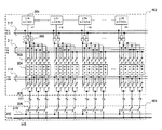
しかしながら、このような構成を採用しているため、有機EL素子の発光強度はTFTの特性に非常に敏感に影響を受ける。特に、ポリシリコンTFT、中でも低温ポリシリコンと呼ばれる低温プロセスで形成されるポリシリコンTFTは、隣接画素間においても比較的大きな電気的特性の違いが生じることが確認されており、有機ELディスプレイの表示品質、特に画面内の表示均一性を劣化させる大きな要因の一つとなっている。それを改善する従来技術が下記の特許文献に開示されている。この従来技術では、図12に示すように、有機EL素子290を電流駆動するTFT260が、データライン220に流す階調電流を流すように制御する手段を開示している。
However, since such a configuration is adopted, the light emission intensity of the organic EL element is very sensitively influenced by the characteristics of the TFT. In particular, it has been confirmed that polysilicon TFTs, especially polysilicon TFTs formed by a low-temperature process called low-temperature polysilicon, have a relatively large difference in electrical characteristics between adjacent pixels. This is one of the major factors that degrade the quality, particularly the display uniformity within the screen. Prior arts for improving this are disclosed in the following patent documents. As shown in FIG. 12, this prior art discloses means for controlling the TFT 260 that drives the
図12に示す従来技術の手段を用いると、データライン220に流す階調電流は、所定の手続きにより駆動TFT260に流されることで、駆動TFT260がデータライン220に流れた階調電流を流すことのできる電圧が生成されて保持容量280に電荷が蓄積される(電流を書き込む)。駆動TFT260は、次にアクセスされるまで有機EL素子290に前記階調電流を流し続けるため、所望の階調を得ることができる。
When the prior art means shown in FIG. 12 is used, the gradation current that flows through the data line 220 is caused to flow through the driving TFT 260 according to a predetermined procedure, so that the driving TFT 260 causes the gradation current that flows through the data line 220 to flow. A voltage that can be generated is generated, and electric charge is accumulated in the storage capacitor 280 (current is written). The driving TFT 260 continues to pass the gradation current through the
ところで、データライン220に流す階調電流は、R、B、Gのビデオ信号を入力しこれを電圧電流変換する電圧電流回路を有するデータドライバによってデータラインに供給されるが、電圧電流変換回路内のTFTを低温ポリシリコンプロセスで形成すると、均一な電圧電流変換特性を得ることが困難であり、特性不均一による画質劣化を生じる問題がある。 By the way, the gray-scale current flowing through the data line 220 is supplied to the data line by a data driver having a voltage-current circuit that inputs R, B, and G video signals and converts them into voltage-current. When the TFT is formed by a low-temperature polysilicon process, it is difficult to obtain uniform voltage-current conversion characteristics, and there is a problem that image quality is deteriorated due to non-uniform characteristics.
本発明の目的は、データラインにデータ信号を供給する電圧電流変換回路の特性バラツキを抑制することができる表示装置を提供することにある。 An object of the present invention is to provide a display device that can suppress variation in characteristics of a voltage-current conversion circuit that supplies a data signal to a data line.
本発明は、電流駆動されるダイオード型発光素子と前記ダイオード型発光素子を制御する薄膜トランジスタとを1つの画素回路として、前記画素回路をマトリクス状に配置したアクティブマトリクス型表示アレイと、前記マトリクスの各列に対応して設けられ、対応する列の画素回路にデータ信号を供給するデータラインと、前記データラインへの前記データ信号の供給を制御するデータドライバと、前記マトリクスの各行に対応して設けられ、対応する行の画素回路に選択信号を供給するゲートラインと、前記ゲートラインに選択信号を供給するゲートドライバと、前記データドライバ及びゲートドライバを制御する制御回路とを有するアクティブマトリクス型表示装置であって、前記データドライバは、入力されたビデオ信号を電圧電流変換して前記データ信号として前記データラインに出力する電圧電流変換回路を有し、前記電圧電流変換回路はビデオ信号に対して複数系統設けられ、前記複数系統の電圧電流変換回路をフレーム毎あるいはライン毎の少なくともいずれかで切り替えられ、前記電圧電流変換回路に入力される前記ビデオ信号は複数系統設けられ、前記複数系統のビデオ信号は前記データライン毎に切り替えられ、前記画素回路は、一端の電位が所定電位に固定された保持容量と、前記保持容量の非固定電位端子に一方の非制御端子が接続され、他方の非制御端子が前記データラインに接続され、制御端子が前記ゲートラインに接続されたゲートトランジスタと、制御端子が前記保持容量の非固定電位端子に接続され、一方の非制御端子が電源ラインに接続されて前記ダイオード型発光素子への駆動電流を制御する駆動トランジスタと、制御端子が点灯ラインに接続され、一方の非制御端子が前記駆動トランジスタの他方の非制御端子に接続され、他方の非制御端子が前記ダイオード型発光素子に接続されて前記ダイオード型発光素子の駆動電流のオンオフを制御する点灯制御トランジスタとを有し、画素回路の駆動時に、前記駆動トランジスタのゲート端子に前記データラインに流れた階調電流を前記駆動トランジスタが流すためのゲート電位が生成され、安定化した後、前記点灯制御トランジスタをオンし、前記ダイオードトランジスタも逆バイアスが印加され、前記データラインからの階調電流が前記駆動トランジスタを経由して流れなくなり、その後、前記ゲートトランジスタをオフすることで、前記保持容量に、前記データラインに流れた階調電流を前記駆動トランジスタが流すための電位が書き込まれ、次のアクセスまで保持するようにしたことを特徴とする。
The present invention relates to an active matrix display array in which a pixel-type light-emitting element driven by current and a thin-film transistor that controls the diode-type light-emitting element are used as one pixel circuit, and the pixel circuits are arranged in a matrix. A data line that is provided corresponding to the column and supplies a data signal to the pixel circuit in the corresponding column; a data driver that controls the supply of the data signal to the data line; and a data line that corresponds to each row of the matrix Active matrix type display device comprising: a gate line that supplies a selection signal to the pixel circuit in the corresponding row; a gate driver that supplies the selection signal to the gate line; and a control circuit that controls the data driver and the gate driver. The data driver converts the input video signal into a voltage current. In other words, a voltage-current conversion circuit that outputs the data signal to the data line is provided. The voltage-current conversion circuit is provided in a plurality of systems for a video signal, and the plurality of systems of voltage-current conversion circuits are arranged for each frame or line. The video signals that are switched at least at any one of them and input to the voltage-current conversion circuit are provided in a plurality of systems, the video signals of the plurality of systems are switched for each data line , and the pixel circuit has a potential at one end. Is connected to the storage capacitor, the non-fixed potential terminal of the storage capacitor is connected to one non-control terminal, the other non-control terminal is connected to the data line, and the control terminal is connected to the gate line. And the control terminal is connected to the non-fixed potential terminal of the storage capacitor, and one non-control terminal is connected to the power supply line. A drive transistor for controlling a drive current to the diode-type light emitting element, a control terminal is connected to the lighting line, one non-control terminal is connected to the other non-control terminal of the drive transistor, and the other non-control terminal And a lighting control transistor connected to the diode-type light-emitting element and controlling on / off of the drive current of the diode-type light-emitting element, and flows to the data line at the gate terminal of the drive transistor when the pixel circuit is driven A gate potential for causing the driving current to flow through the driving transistor is generated and stabilized, and then the lighting control transistor is turned on, the diode transistor is also applied with a reverse bias, and the gradation current from the data line is No longer flows through the drive transistor, then turn off the gate transistor Thus, the storage capacitor is written with a potential for causing the driving transistor to pass the gradation current that has flowed to the data line, and is held until the next access .
本発明における切替の態様は、フレーム毎の切り替え、ライン毎の切り替え、フレーム毎かつライン毎の切り替え、の3態様である。また、本発明において、R信号、G信号、B信号の少なくともいずれかに対して複数系統設けることが好適である。1つの態様は、R信号、G信号、B信号それぞれに対して2系統の電圧電流変換回路を設けるものである。複数の電圧電流変換回路を第1系統及び第2系統とした場合、奇数フレームにおいては奇数ラインのデータラインは前記第1系統で駆動するとともに偶数ラインのデータラインは前記第2系統で駆動制御し、偶数フレームにおいては奇数ラインのデータラインは前記第2系統で駆動するとともに偶数ラインのデータラインは前記第1系統で駆動制御することが好適である。もちろん、電圧電流変換回路を3系統あるいはそれ以上設けてもよい。本発明において、電圧電流変換回路に入力されるビデオ信号自体を複数系統設け、これらのビデオ信号をデータライン毎に切り替えてもよく、さらにフレーム毎あるいはライン毎の少なくともいずれかで切り替えてもよい。複数系統設けられたビデオ信号と電圧電流変換回路の組合せで多様な特性が実現できる。 The mode of switching in the present invention is three modes: switching for each frame, switching for each line, and switching for each frame and each line. In the present invention, it is preferable to provide a plurality of systems for at least one of the R signal, the G signal, and the B signal. In one embodiment, two voltage-current conversion circuits are provided for each of the R signal, the G signal, and the B signal. When the plurality of voltage-current conversion circuits are the first system and the second system, in odd frames, the odd-numbered data lines are driven by the first system and the even-numbered data lines are driven and controlled by the second system. In an even frame, it is preferable that the odd-numbered data lines are driven by the second system and the even-numbered data lines are driven and controlled by the first system. Of course, three or more voltage-current conversion circuits may be provided. In the present invention, a plurality of video signals input to the voltage-current conversion circuit may be provided, and these video signals may be switched for each data line, and may be switched for each frame or for each line. Various characteristics can be realized by a combination of video signals and voltage-current conversion circuits provided in a plurality of systems.
本発明によれば、データラインにデータ信号を供給する電圧電流変換回路を複数系統設け、これらを切り替えてデータ信号を供給するため、電圧電流変換回路の特性バラツキを低減できる。 According to the present invention, since a plurality of voltage-current conversion circuits that supply data signals to the data lines are provided and the data signals are supplied by switching them, variation in characteristics of the voltage-current conversion circuits can be reduced.
以下、図面を用いて本発明の実施の形態を詳細に説明する。 Hereinafter, embodiments of the present invention will be described in detail with reference to the drawings.
(1)第1実施形態
<全体構成>
図1には、本実施形態における有機ELディスプレイの全体構成図が示されている。有機ELディスプレイ1は、画素に有機EL素子とTFTを配置したアクティブマトリクス型表示アレイ101、データドライバ102、ゲートドライバ103、プリチャージ回路104、データ制御バス112を介してデータドライバ102にビデオ信号と制御信号を供給するとともにゲート制御バス113を介してゲートドライバ103に制御信号を供給する制御回路106、データドライバ102からの階調データ電流もしくはプリチャージ回路104からのプリチャージ電圧を画素に供給するデータライン107、ゲートドライバ103からのゲート選択電位を供給するゲートライン108、ゲートドライバ103から有機EL素子を点灯制御する制御電圧を供給する点灯ライン109、及びRGBの映像データ及びクロック等が入力される入力バス111を有して構成される。表示アレイ101、データドライバ102、ゲートドライバ103、プリチャージ回路104で表示デバイスが構成され、低温ポリシリコンプロセスを適用すれば、これらの回路はガラス基板上に形成できる。
(1) First Embodiment <Overall Configuration>
FIG. 1 shows an overall configuration diagram of an organic EL display according to the present embodiment. The
<画素回路構成>
次に、図2を用いて、アクティブマトリクス型表示アレイ101内にマトリクス状に配置されている本実施形態の画素回路の回路構成を説明する。
<Pixel circuit configuration>
Next, the circuit configuration of the pixel circuit of this embodiment arranged in a matrix in the active
画素回路は、有機EL素子201、有機EL素子201を電流駆動する駆動TFT202、駆動TFT202のゲート端子とドレイン端子を接続するダイオードTFT203、有機EL素子201を点灯するか否か(電流を流すか流さないか)を制御する点灯制御TFT204、データライン107からの階調電流を画素内へ供給制御するゲートTFT205、保持容量206、有機EL素子201に電流を供給する電流供給ライン211、保持容量206の一方の端子電位を所定値に固定する固定電位ライン212を有して構成される。固定電位ライン212は電流供給ライン211に接続されていてもよい。
The pixel circuit includes an
駆動TFT202のソース端子は電流供給ライン211に、ドレイン端子は点灯制御TFT204のソース端子とダイオードTFT203のソース端子に、ゲート端子は保持容量206の固定電位ライン212に接続されていない片方の端子とゲートTFT205のソース端子、ダイオードTFT203のドレイン端子にそれぞれ接続される。点灯制御TFT204のゲート端子は点灯ライン109に接続され、点灯制御TFT204のドレイン端子は有機EL素子201のアノードに接続される。ゲートTFT205のゲート端子はゲートライン108に、ドレイン端子はデータライン107に接続される。電流供給ライン211、固定電位ライン212、有機EL素子201のカソード電極はすべての画素で共有されている。
The source terminal of the driving TFT 202 is connected to the
データドライバ102、ゲートドライバ103、プリチャージ回路104を用いて図2の画素回路を制御する方法に関しては後述するが、以下に図2の画素を用いて有機EL素子を駆動する方法を説明する。
A method for controlling the pixel circuit in FIG. 2 using the
<駆動方法>
A.プリチャージ
まず、ゲートTFT205をオンし、保持容量206にプリチャージ電位を書き込む。このプリチャージ電位は有機EL素子201が消灯するレベル、つまり電流が流れないレベルとする。そうすると、有機EL素子201に流れていた電流は徐々に減少し、やがて流れなくなる。図2の画素回路は階調電流を書き込む直前は常にこの初期状態となるように制御する。つまり、有機EL素子201は消灯、駆動TFT202のゲート電位とデータライン107の電位はプリチャージ電位となるようにする。
<Driving method>
A. Precharge First, the
B.駆動
次に、点灯制御TFT204をオフし、駆動TFT202のドレイン端子をハイインピーダンスにする。そして、ゲートTFT205をオンし、データライン107に階調電流を流すと、その電流は、電流供給ライン211から駆動TFT202のソース端子からドレイン端子を通り、ダイオードTFT203の順方向を経由し、ゲートTFT205を通ってデータライン107に流れる。これにより、駆動TFT202のゲート端子には、データライン107に流した階調電流を駆動TFT202が流すためのゲート電位が生成される。この電位が安定した後、点灯制御TFT204をオンすると、ダイオードTFT203に逆バイアスが印加され、データライン107からの階調電流が駆動TFT202を経由して流れなくなる。その後、ゲートTFT205をオフすることで、保持容量206には、データライン107に流された階調電流を駆動TFT202が流すための電位が書き込まれ、次にアクセスされるまで保持される。ここで、ダイオードTFT203に逆バイアスが印加される理由について説明する。駆動TFT202は通常飽和領域で用いられるため、駆動TFT202のドレイン・ソース間電圧Vdsは、点灯制御TFT204がオンする、すなわち有機EL素子201と接続されると、駆動TFT202のゲート・ソース間電圧Vgsに対して、十分大きく、|Vds|>|Vgs|が成立する。そのため、ダイオードTFT203には逆バイアスが印加され、データライン107への電流経路が絶たれることになる。以降、図2の画素回路は再び前記初期状態に戻され、階調電流が書き込まれるという上記動作を繰り返す。
B. Driving Next, the
<データドライバ及びプリチャージ回路>
次に、図2の画素回路がマトリクス状に配置された表示アレイ101を前述のように駆動するために用いるデータドライバ102、プリチャージ回路104について、図3を用いてその内部構成を説明する。
<Data driver and precharge circuit>
Next, the internal configuration of the
データドライバ102は、シフトレジスタ301、イネーブル回路302、ビデオスイッチ303、電圧電流変換回路304、データスイッチ305、RGBのビデオ信号ライン311、ドライバセレクトライン312(EA、EB)、アウトプットイネーブルライン313(OA、OB)を有して構成される。また、プリチャージ回路104は、プリチャージスイッチ306、プリチャージイネーブルライン314(PRE)、プリチャージ電位供給ライン315を有して構成される。図3はRGBそれぞれ1系統の入力を有するデータドライバ構成、プリチャージ回路構成を示している。
The
シフトレジスタ301は入力パルスをクロックに同期して順次シフトレジスタ1からnまでシフトする。出力端子Hi(i=1〜n)には入力パルスをシフトしたパルスが出力され、それぞれのパルスイネーブル回路302に入力される。
The
パルスイネーブル回路302はドライバセレクトライン312のEA、EBによってシフトレジスタ出力をイネーブルする。
The pulse enable
ビデオスイッチ303、電圧電流変換回路304、データスイッチ305は、RGBそれぞれ系統A及び系統Bの2系統用意されている。まず、ドライバセレクト信号ラインEA、EBにより、パルスイネーブル回路302を介してイネーブルされたシフトレジスタのシフトパルスによって、系統A、系統Bいずれかのビデオスイッチ303がオンし、ビデオ信号ライン311がA、Bいずれかの電圧電流変換回路304に接続される。例えば、シフトレジスタ1の出力H1が“High”、EAを“High”、EBを“Low”とすると、シフトレジスタ1のパルスイネーブル回路302はシフトレジスタのシフトパルスを系統Aのビデオスイッチ303へ伝播し、その系統Aのビデオスイッチは、系統Aの電圧電流変換回路RA1、GA1、BA1の入力を、ビデオ信号ラインR、G、Bと接続し、ビデオデータをそれぞれの電圧電流変換回路内へ取り込む。シフトパルスが最後のシフトレジスタnまで行き渡り、水平ラインのデータが系統A及び系統Bいずれかの電圧電流変換回路304にサンプルされると、サンプルした系統のOAもしくはOBのアウトプットイネーブルラインをアクティブにし、データライン107とアクティブにされた系統の電圧電流変換回路304の出力を接続し、データライン107を駆動する。EAを“High”とした上記の例に従えば、シフトレジスタnまでシフトパルスが行き渡ったのち、OAをアクティブとすることで、データライン107を系統Aの電圧電流変換回路304で駆動することになる。
The
ビデオ信号ライン311に着目すると、ビデオ信号ライン311はビデオスイッチ303によって電圧電流変換回路304に接続される。したがって、ビデオ信号ライン311の配線負荷は、ビデオスイッチ303によって接続された電圧電流変換回路304の入力インピーダンスに等しく、非常に小さい。これはビデオ信号ライン311上の信号をより高速に電圧電流変換回路304に転送できることを意味し、より高解像度なパネルを駆動するのに適している。
Focusing on the
電圧電流変換回路304は、図2のように駆動TFT202をPチャネル型TFTで構成した場合、例えば図15に示すNチャネル型TFTで構成するのが望ましい。最も簡単な回路は図15(a)に示す例である。Nチャネル型の電圧電流変換TFT1501、及び保持容量1502で構成される。
When the driving
再び図3に戻り、電圧電流変換TFT1501は、シフトレジスタ301のシフトパルスと、ドライバセレクトラインEA、EBで制御されるビデオスイッチ303により順次データバス311上のデータをサンプルし、サンプルした電圧レベルに応じて電流値を決定する。一ライン分のデータをサンプルし終えると、アウトプットイネーブルラインOA、OBにより制御されるデータスイッチ305により、データライン107に接続され、保持容量1502に保持されている階調電圧に対応する階調電流でデータライン107を駆動する。
Returning to FIG. 3 again, the voltage-
電圧電流変換回路1501は例えば低温ポリシリコンTFTプロセスで形成されると、均一な電圧電流変換特性を得ることが困難であるため、図15(b)に示すように、リセットTFT1503、1504及びリセット容量1505を追加し、電圧電流変換TFT1501の閾値電圧Vth補正を行うことでより電圧電流変換特性の均一性を向上できる。
When the voltage-
<閾値電圧Vthの補正>
リセットTFT1503、1504及びリセット容量1505を用いて電圧電流変換TFT1501のVthを補正する手順について説明する。
<Correction of threshold voltage Vth>
A procedure for correcting Vth of the voltage-
まず、シフトレジスタに入力パルスを入力する前、すなわちビデオスイッチ303をオフとし、データスイッチ305をオフして、リセットTFT1503、1504をオンすると、TFT1501に流れていた電流はやがてゼロに近づく。すなわち、リセット容量1505に電圧電流変換TFT1501のVthが書き込まれる。
First, before an input pulse is input to the shift register, that is, when the
次いで、リセットTFT1503、1504をオフし、シフトレジスタに入力パルスを入力し、順次データバス311上の階調電圧データを1502に取り込むことで電圧電流変換TFT1501のゲート電位Vgsは、階調電圧をVdとすると、Vgs=Vth+Vdに設定される。
Next, the
このように電圧電流変換回路304に補正回路を付加することで電圧電流変換のばらつきを低減できる。なお電圧電流変換TFT1501は変換特性の均一性を向上させるため、リセットTFT1503、1504などと比較してより大きく設計することが望ましい。
Thus, by adding a correction circuit to the voltage /
一方、プリチャージ回路104は、プリチャージスイッチ306を含み、プリチャージイネーブルライン314であるPREをアクティブにすることでデータライン107をプリチャージ電位供給ライン315に接続し、所定のプリチャージ電位VPREにデータライン107をプリチャージする。
On the other hand, the
データライン107はデータドライバ102とプリチャージ回路104によって駆動されるため、データライン107がプリチャージを行っている間、電圧電流変換回路のVthリセットを行えばよい。
Since the
このデータドライバ102は以上の説明で述べた機能、もしくはそれに準ずる機能を有するデータドライバICを代わりに用いることもできる。
As the
<ゲートドライバ>
次に図4を用いてゲートドライバ103の内部構成を説明する。ゲートドライバ103は、シフトレジスタ401、ゲートイネーブル回路402、点灯イネーブル回路403、ゲートバッファ404、点灯バッファ405を有して構成される。図において、E1、E2はそれぞれ奇数ライン、偶数ラインのゲートイネーブル制御ライン、LEは点灯イネーブル制御ラインである。
<Gate driver>
Next, the internal configuration of the
奇数ラインのゲートイネーブル回路402の1入力はゲートイネーブル制御ラインE1に接続され、偶数ラインのゲートイネーブル回路402の1入力はゲートイネーブル制御ラインE2に接続されている。全ラインの点灯イネーブル回路403の1入力は点灯イネーブル制御ラインLEに接続されている。
One input of the odd-numbered gate enable
また各ラインのイネーブル回路402、403のもう1入力は各シフトレジスタ出力Vi(i=0〜n)に接続され、シフトレジスタ出力ViとE1、E2、LEにより、各ゲートライン108、点灯ライン109の状態を制御する。
The other inputs of the
<フレーム期間の表示状態>
図5には、横軸に時間、縦軸に表示ラインをとり、本実施形態のフレーム期間の表示状態が示されている。各ラインは、1フレーム期間を、映像データを表示する表示期間と、有機EL素子201及び駆動TFT202をリセットするリセット期間に分割される。ここで「リセットする」とは、駆動TFT202のゲート端子に、電流が流れない電位(プリチャージ電位VPRE)を設定して有機EL素子201を消灯する動作を言う。また、「リセット期間」とは、その電位が保持容量206に書き込まれることで、次に表示データのためのアクセスが行われるまで、前記リセット状態が維持される期間を言う。
<Display status of frame period>
FIG. 5 shows the display state of the frame period of the present embodiment, with time on the horizontal axis and display lines on the vertical axis. Each line is divided into one frame period into a display period for displaying video data and a reset period for resetting the
このように表示期間を分割した理由は、表示期間を短縮することで書き込み電圧の保持期間も同様に短縮でき、TFTのリーク電流の影響が低減されること、さらにブラウン管のような発光特性を擬似的に行うことができ、動画視認性を向上させられるためである。 The reason for dividing the display period in this way is that the retention period of the write voltage can be shortened by shortening the display period, the influence of the leakage current of the TFT is reduced, and the light emission characteristics such as a cathode ray tube are simulated. This is because the visibility of the moving image can be improved.
まず第1ラインから映像データを順次書き込み、ある期間を置いて、全ラインの映像データの書き込みを終える前に、すでに映像データに応じた電流を流している駆動TFT202のリセットを複数回に分けて第1ラインから順次行う。図5において、X−X’区間に着目すると、第k0ラインは映像データの書き込みが行われ、第k1ラインは第1のリセット動作、第k2ラインは第2のリセット動作が行われている。
First, the video data is sequentially written from the first line, and after a certain period of time, before completing the writing of the video data of all the lines, the resetting of the driving
図6、図7を用いて、データドライバ102、ゲートドライバ103、プリチャージ回路104を制御して図5の表示を行う方法についてさらに説明する。
A method for performing the display of FIG. 5 by controlling the
図6において、ゲートドライバ103のシフトレジスタ401に入力する入力パルス601、入力パルス601をシフトするためのクロック602、シフトレジスタ出力V1のシフトパルス603が示されており、このパルスが順次シフトされ、Viに出力されていく。また、第k0ラインのシフトレジスタ出力パルス604、第k1ラインのシフトレジスタ出力パルス605、第k2ラインのシフトレジスタ出力パルス606が示され、X−X’区間ではいずれもアクティブである。
In FIG. 6, an
図7において、X−X’区間におけるシフトレジスタ出力Vk0、Vk1、Vk2の出力パルス701、同区間におけるシフトレジスタ出力Vk0+1、Vk1+1、Vk2+1の出力パルス702、イネーブル制御ラインE1のパルス703、イネーブル制御ラインE2のパルス704、点灯イネーブル制御ラインLEのパルス705、プリチャージ制御ラインPREのパルス706、データドライバ102のシフトレジスタに入力する入力パルス707、系統Aドライバセレクトラインのパルス708、系統Bドライバセレクトラインのパルス709、系統AアウトプットイネーブルOAのパルス710、系統BアウトプットイネーブルOBのパルス711、データライン107のデータ電位712がそれぞれ示されている。
In FIG. 7, shift register outputs Vk0, Vk1, and
図7ではk0は奇数、k1、k2は偶数となるように、入力パルス601を入力しているものとすると、X−X’区間の前半であるX−Y区間は、E1が“H”、LEが“H”、プリチャージがイネーブルされていることから、k0ラインはプリチャージされる。同時にE2も“H”であるから、k1、k2ラインもプリチャージされる。この間、データライン107はプリチャージ電位VPREにプリチャージされ、ゲートTFT205がオンすることから、保持容量206にはプリチャージ電位VPREが書き込まれる。このプリチャージ電位VPREは駆動TFT202をオフするレベル、つまり電流供給ライン211の電位レベルに近い電位である。
In FIG. 7, assuming that the
X−X’区間の後半であるY−X’区間は、LEが“H”、E1が“H”、E2が“L”、プリチャージがディスエーブル、OAが“H”であるから、k0のみデータドライバ102の系統Aの電圧電流変換回路により電流データ書き込みを行う。
In the YX ′ section which is the latter half of the XX ′ section, LE is “H”, E1 is “H”, E2 is “L”, precharge is disabled, and OA is “H”. Only current data is written by the voltage-current conversion circuit of the system A of the
このように、X−X’区間ではk0ラインはリセット後データを書き込み、k1、k2ラインはリセットのみ行われている。ここで、データライン107に供給される階調電流データは、各水平期間に入力される入力パルス707がシフトレジスタ301により順次シフトされ、データバス311上のデータをセレクトラインEA、EBが選択する系統の電圧電流変換回路304に取り込まれた後、データを取り込んだ系統を選択するアウトプットイネーブルOA、OBで選択される電圧電流変換回路304で出力された電流データである。つまり、YX’区間にデータライン107に出力される電流データは、この場合、一水平期間前に系統Aに順次取り込まれたデータに対応する。YX’区間のデータ書き込み区間にデータライン107に階調電流が供給されると、第k0ラインの画素内の駆動TFT202には、ゲートTFT205がオン、点灯制御TFT204がオフであるため、電流供給ライン211から駆動TFT202のソース、ドレインを通り、ダイオードTFT203を経由し、ゲートTFT205を通ってデータドライバへ階調電流が流れる。
Thus, in the X-X 'interval, the k0 line is written with data after reset, and the k1 and k2 lines are only reset. Here, in the gradation current data supplied to the
保持容量206にはあらかじめプリチャージ電位VPREが書き込まれているため、駆動TFT202に階調電流が流れ始めると、徐々に駆動TFT202のゲート電位はプリチャージ電位からデータライン107に流れる階調電流を駆動TFT202が流すことのできる電位へ変化する。その後、点灯制御TFT204をオンすると、前記理由により、ダイオードTFT203には逆バイアスが印加されるため、データライン107に流れていた電流の経路が遮断され、その後、ゲートTFT205をオフすることで、保持容量206にデータライン107に流れていた階調電流を駆動TFT202が流す電圧が保持される。
Since the precharge potential VPRE is written in the
次に、X’−Y’区間に入ると、第k0ラインはVk0が”L”となるため、書き込まれたデータの表示を維持し、次のシフトパルスが入力されるまで、書き込まれた階調電流で有機EL素子201に電流を流し続ける。第k1ラインは点灯が終了し、消灯期間に入る。この際、有機EL素子201に流れていた電流は徐々に減少し、ある時間を経てゼロになる。第k2ラインはすでに消灯期間に入っており、引き続き有機EL素子201の消灯を続ける。ここで、第k2ラインのように複数回リセットする理由は、プリチャージ期間XY、あるいはX’−Y’期間が十分に確保できない場合、より確実にリセット可能とするためである。したがって、さらに何度もリセット書き込みを行ってもよい。
Next, when entering the section X′-Y ′, Vk0 becomes “L” in the k0th line, so that the display of the written data is maintained and the written level is kept until the next shift pulse is input. The current continues to flow through the
X’−X’’区間では、偶数ラインのk0+1ライン、奇数ラインのk1+1、k2+1は、その前半X’−Y’で、両者ともリセット期間となり、後半Y’−X’’でk0+1ラインのみ電流データを書き込む。ここで、データライン107上の電流データは、X’−X’’区間の1水平期間前、つまりX−X’区間で系統Bの電圧電流変換回路にサンプルした電圧データが電流データに変換されたデータであり、アウトプットイネーブルOBをアクティブにすることで系統B電流電圧変換回路がデータライン107を駆動したものである。
In the interval X′−X ″, the k0 + 1 line of the even line and the k1 + 1 and k2 + 1 of the odd line are both in the first half X′−Y ′, and both are in the reset period, and only the k0 + 1 line is in the second half Y′−X ″. Write data. Here, the current data on the
このように電流電圧変換回路304は、系統Aと系統Bで交互にデータライン107を駆動する。しかし、系統Aと系統Bの電圧電流変換回路には図15のようなVth補正を施しても、系統間で電流出力に違いが生じる可能性がある。
Thus, the current-
そこで、系統の切り替えをフレーム毎に変化させる。例えば、奇数フレームで奇数ラインを系統Aが駆動することに決めると、偶数ラインは系統Bで駆動することになる。次の偶数フレームでは偶数ラインを系統Aで駆動し、奇数ラインを系統Bで駆動するように制御すれば、すべての画素がフレーム毎にどちらの電圧電流変換回路でも駆動されるため電流出力ばらつきの表示に対する影響を低減できる。あるいは、系統A、Bいずれかの系統のみ、つまり1系統の電圧電流変換回路304で駆動することも可能である。前述したように、データドライバ102は、ビデオ信号ライン311上のビデオデータを高速に電圧電流変換回路304にデータ転送可能である。そのため、図7におけるXY区間のプリチャージ期間に1ライン分のデータを電圧電流変換回路304へ転送し、残りのYX’区間で出力をイネーブルして電流データを書き込むという駆動が可能である。このような駆動をする場合、複数の系統を設けることは、冗長な構成となるが、回路不良や、電圧電流変換特性の不均一等に起因するドライバ不良による歩留まり低下を抑制することができる。
Therefore, the system switching is changed for each frame. For example, if the system A decides to drive the odd lines in the odd frame, the even lines are driven by the system B. In the next even frame, if the even lines are driven by the system A and the odd lines are driven by the system B, all the pixels are driven by either voltage-current conversion circuit every frame, so that the current output variation The influence on the display can be reduced. Alternatively, it is possible to drive only one of the systems A and B, that is, the voltage /
もちろん、系統の切り替えの態様は、上記に限定されるものではない。例えば単に奇数フレームでは系統Aで駆動し、偶数フレームでは系統Bで駆動することも可能である。フレームによらず、奇数ラインは系統Aで駆動し、偶数ラインは系統Bで駆動してもよい。また、R信号、G信号、B信号それぞれに系統A、系統Bを設けるのではなく、いずれか1つ又は2つの色信号のみに系統A、系統Bを設けてもよい。例えば、B信号のみを系統A、系統Bにしてフレーム毎あるいはライン毎に切り替える等である。特性のバラツキを特に特定したい色信号に着目し、当該色信号を複数系統にすればよい。 Of course, the mode of system switching is not limited to the above. For example, it is possible to simply drive with the system A in the odd frame and drive with the system B in the even frame. The odd lines may be driven by the system A and the even lines may be driven by the system B regardless of the frame. In addition, the system A and the system B may not be provided for the R signal, the G signal, and the B signal, but the system A and the system B may be provided for only one or two color signals. For example, only the B signal is changed to the system A and the system B and switched for each frame or each line. Focusing on the color signal for which the characteristic variation is particularly desired to be specified , the color signal may be made into a plurality of systems.
また、電圧電流変換回路304を複数系統設けるとともに、電圧電流変換回路304に供給されるビデオ信号自体も複数系統設け、これらを適宜切り替えるように構成してもよい。すなわち、図3の例では、一つのビデオ信号を分けて系統Aと系統Bに供給しているが、ビデオ信号自体を第1のビデオ信号(R1、G1、B1)と第2のビデオ信号(R2、G2、B2)を有する2系統のビデオ信号とする。これらの第1ビデオ信号及び第2のビデオ信号は、シフトレジスタ301からの信号により、2系統のビデオ信号ラインの3つずつ(合計6ライン)を電圧電流変換回路304に供給する。これにより、シフトレジスタ301の1パルスで2倍の画素のビデオ信号をサンプルホールドできるため、より高解像度のパネルを駆動することができる。第1ビデオ信号と第2ビデオ信号は、データライン毎に切り換えることができ、例えばあるデータラインを第1ビデオ信号で駆動するものとすると、そのデータラインに隣接する同色のデータライン(隣接する同色画素:R画素であれば隣接する次のR画素)は第2ビデオ信号で駆動する。第1ビデオ信号あるいは第2ビデオ信号のいずれを電圧電流変換回路304で電流変換するかは、フレーム毎あるいはライン毎に切り替え制御することができる。その一つの例は以下の通りである。すなわち、第1ビデオ信号と第2ビデオ信号をデータライン毎に切り替え、しかもフレーム毎かつライン毎に切り替えるものとし、第1データライン及び第2データラインを互いに隣接する同色のデータラインであるとして、
<奇数フレーム>
奇数ライン→第1データラインは第1ビデオ信号、第2データラインは第2ビデオ信号
偶数ライン→第1データラインは第2ビデオ信号、第2データラインは第1ビデオ信号
<偶数フレーム>
奇数ライン→第1データラインは第2ビデオ信号、第2データラインは第1ビデオ信号
偶数ライン→第1データラインは第1ビデオ信号、第2データラインは第2ビデオ信号
がそれぞれ電圧電流変換回路304に供給されるものとする。このような切り替え制御に対し、上記のように電圧電流変換回路304自体も系統Aと系統Bとがフレーム毎あるいはライン毎に切り替え制御されるから、両者の組合せにより、例えば以下のような切り替えが行われる。
In addition, a plurality of voltage /
<Odd frame>
Odd line → first data line is first video signal, second data line is second video signal even line → first data line is second video signal, second data line is first video signal <even frame>
The odd number line → the first data line is the second video signal, the second data line is the first video signal, the even number → the first data line is the first video signal, and the second data line is the second video signal. Suppose that it is supplied to 304. For such switching control, the voltage-
<奇数フレーム>
奇数ライン→第1データラインは第1ビデオ信号を系統Aで駆動し、第2データライン は第2ビデオ信号を系統Aで駆動
偶数ライン→第1データラインは第2ビデオ信号を系統Bで駆動し、第2データライン は第1ビデオ信号を系統Bで駆動
<偶数フレーム>
奇数ライン→第1データラインは第2ビデオ信号を系統Bで駆動し、第2データライン は第1ビデオ信号を系統Bで駆動
偶数ライン→第1データラインは第1ビデオ信号を系統Aで駆動し、第2データライン は第2ビデオ信号を系統Aで駆動
もちろん、これら以外にも任意の組合せが可能であり、例示すると、
<奇数フレーム>
奇数ライン→第1データラインは第2ビデオ信号を系統Aで駆動し、第2データライン は第1ビデオ信号を系統Aで駆動
偶数ライン→第1データラインは第1ビデオ信号を系統Bで駆動し、第2データライン は第2ビデオ信号を系統Bで駆動
<偶数フレーム>
奇数ライン→第1データラインは第1ビデオ信号を系統Bで駆動し、第2データライン は第2ビデオ信号を系統Bで駆動
偶数ライン→第1データラインは第2ビデオ信号を系統Aで駆動し、第2データライン は第1ビデオ信号を系統Aで駆動
あるいは、
<奇数フレーム>
奇数ライン→第1データラインは第1ビデオ信号を系統Aで駆動し、第2データライン は第2ビデオ信号を系統Aで駆動
偶数ライン→第1データラインは第2ビデオ信号を系統Bで駆動し、第2データライン は第1ビデオ信号を系統Bで駆動
<偶数フレーム>
奇数ライン→第1データラインは第1ビデオ信号を系統Bで駆動し、第2データライン は第2ビデオ信号を系統Bで駆動
偶数ライン→第1データラインは第2ビデオ信号を系統Aで駆動し、第2データライン は第1ビデオ信号を系統Aで駆動
あるいは、
<奇数フレーム>
奇数ライン→第1データラインは第2ビデオ信号を系統Aで駆動し、第2データライン は第1ビデオ信号を系統Aで駆動
偶数ライン→第1データラインは第1ビデオ信号を系統Bで駆動し、第2データライン は第2ビデオ信号を系統Bで駆動
<偶数フレーム>
奇数ライン→第1データラインは第2ビデオ信号を系統Bで駆動し、第2データライン は第1ビデオ信号を系統Bで駆動
偶数ライン→第1データラインは第1ビデオ信号を系統Aで駆動し、第2データライン は第2ビデオ信号を系統Aで駆動
等である。これらの組合せのいずれかを選択して切り替え制御すればよい。
<Odd frame>
Odd line → first data line drives the first video signal with system A, second data line drives the second video signal with system A Even line → first data line drives the second video signal with system B The second data line drives the first video signal with system B. <Even number frame>
Odd line → first data line drives second video signal by system B, second data line drives first video signal by system B even line → first data line drives first video signal by system A In addition, the second data line can drive the second video signal by the system A. Of course, any other combination is possible. For example,
<Odd frame>
Odd line → first data line drives second video signal by system A, second data line drives first video signal by system A Even line → first data line drives first video signal by system B The second data line drives the second video signal with system B. <Even number frame>
Odd line → first data line drives the first video signal by system B, second data line drives the second video signal by system B Even line → first data line drives the second video signal by system A And the second data line drives the first video signal in system A, or
<Odd frame>
Odd line → first data line drives the first video signal with system A, second data line drives the second video signal with system A Even line → first data line drives the second video signal with system B The second data line drives the first video signal with system B. <Even number frame>
Odd line → first data line drives the first video signal by system B, second data line drives the second video signal by system B Even line → first data line drives the second video signal by system A And the second data line drives the first video signal in system A, or
<Odd frame>
Odd line → first data line drives second video signal by system A, second data line drives first video signal by system A Even line → first data line drives first video signal by system B The second data line drives the second video signal with system B. <Even number frame>
Odd line → first data line drives second video signal by system B, second data line drives first video signal by system B even line → first data line drives first video signal by system A The second data line is driven by the system A for the second video signal. Any one of these combinations may be selected and switched.
このように、ビデオ信号を複数系統用意し、かつ、電圧電流変換回路304も複数系統用意することで、高解像度にも対応でき、しかもバラツキの少ない駆動特性が得られる。
In this manner, by preparing a plurality of systems of video signals and also preparing a plurality of systems of voltage /
さらに、入力パルス601のパルス間隔を制御することで、表示期間とリセット期間の割合を可変とすることが可能である。図13には、リセット期間を25%、50%、75%と変化させた場合のドライバ入力データ電圧Vdと輝度との関係が示されている。リセット期間の割合を増加すると表示期間が短くなるため、同じ入力データ電圧Vd(Vdに対応する電流Id)でより暗く制御することができる。同じ輝度を維持するためには駆動TFT202により多くの電流を流すため、ドライバ入力データのダイナミックレンジを大きくするか、もしくは電圧電流変換TFTのコンダクタンスを増加させればよい。一般に、このような電流プログラム方式では、微小電流の書き込み不足が指摘されているが、これは上記本発明の駆動方法で以下のようにその改善が期待できる。
Furthermore, by controlling the pulse interval of the
まず、現在のプログラミングの前にデータライン107を常にプリチャージ電圧にプリチャージしているため、データラインに以前のデータ電位が残らず、書き込み不足が表示に現れにくい。
First, because of the constantly precharged to the precharge voltage of
また、表示期間とリセット期間の割合を可変することができるため、リセット期間を増加することで、プログラム電流を増加させ、微小電流プログラムを回避することができる。 Further, since the ratio between the display period and the reset period can be changed, the program current can be increased and the minute current program can be avoided by increasing the reset period.
しかしながら、将来、有機EL素子の発光効率の向上により、所望の輝度を生じさせる電流値が少なくて済むようになると、上記手段でも微小電流をプログラムする必要が生じてくる。 However, in the future, when the light emission efficiency of the organic EL element is improved to reduce the current value that produces the desired luminance, it becomes necessary to program a minute current using the above means.
そこで、有機EL素子のカソード電極を図18のように構成する。図18は有機EL素子のカソード電極の構成例であり、図18(a)はカソード電極1801の例、図18(b)はカソード電極1803の例である。
Therefore, the cathode electrode of the organic EL element is configured as shown in FIG. 18A and 18B are configuration examples of the cathode electrode of the organic EL element. FIG. 18A shows an example of the
図18(a)のカソード電極1801は平面構成であり、有機EL素子201からの電流は2次元的に流れ、共通端子COMに流れ出ることができる。一方、図18(b)のカソード電極1803は、有機EL素子201が配列されている領域(表示領域)では、データライン107に垂直な方向、つまり1次元的にしか電流が流れない点で異なる。データライン107とカソード電極1801、1803は、異なるメタルレイヤーで積層され、例えば誘電率εの絶縁層を介して絶縁されている。そのため、一般に交差容量C=ε*S/dの静電容量を持っている。ここでSは交差面積、dは絶縁層の厚さである。
The
電圧電流変換回路304からの微小電流は、データライン107を経由して、駆動TFT202に流されるが、電流が微小であるため、その経路であるデータライン107とカソード電極の交差容量に流れる電流が無視できず、限られた水平期間内に十分に駆動TFT202に流すことができない。
A minute current from the voltage-
そこで、図18(a)では、抵抗素子1802を平面カソード電極1801と外部の共通端子COMとの間に配置し、データライン107からの微小電流の外部への流出を抑制し、駆動TFT202へ効果的に流れるようにした。この電極構成は、従来同様、カソードを低精細度のマスクで形成することができるため、安価である。
Therefore, in FIG. 18A, the
図18(b)は、より精細度の高いマスクで形成した例で、データライン107とカソードの交差面積が低減されている。すなわち交差容量が小さいため、交差容量を介しての微小電流の流出も少なく、駆動TFT202に電圧電流変換回路からの微小電流をより効果的に流すことができる。図18(b)においてもカソード端子1803と外部共通端子COMの間に抵抗素子を配置してもよい。図18(b)は精細度の高いマスクを使用するため、コストを要するが、微小電流の流出抑制効果は図18(a)よりも高い。
FIG. 18B shows an example in which a mask with higher definition is formed, and the cross area of the
さらに、本実施形態では、スイッチTFTの逆バイアスリーク電流、外光によるリーク電流の対策も施されている。 Furthermore, in this embodiment, countermeasures against reverse bias leakage current of the switch TFT and leakage current due to external light are taken.
つまり、ゲートTFT205の逆バイアス及び外光リークに関しては、保持容量206に保持される電位が、リセット期間を挿入することで、1フレーム期間必要とせず、リーク電流の影響は表示に現れにくい。また、複数回リセット動作を行うため、プリチャージ電位がリークにより不十分でも補うことができる。
That is, regarding the reverse bias of the
またダイオードTFT203は逆バイアス時、ドレイン端子とゲート端子は常に同電位であるため、リーク電流はソース・ゲート(ドレイン)電圧のみに影響する。これはダイオードTFT203が3端子を有するスイッチTFTである場合と比較するとリーク電流が低減されることを意味する。
Further, when the
このように、本実施形態の画素回路、駆動回路、駆動方法を用いれば、リーク電流の影響が少なく、より良好な表示が可能となる。 As described above, when the pixel circuit, the drive circuit, and the drive method of the present embodiment are used, the influence of the leakage current is small and a better display can be achieved.
(2)第2実施形態
<画素回路>
図16には、本実施形態の画素回路が示されている。図16の画素回路は図2のダイオードTFT203をダイオード223としている以外、図2の画素回路と同じである。ダイオード223のアノードは駆動TFT202のドレイン端子、点灯制御TFT204のソース端子に、カソードは駆動TFT202のゲート端子、保持容量206の電位固定されてない側の端子、ゲートTFT205のソース端子に接続されている。駆動方法は第1実施形態と同一であるため説明は省略する。
(2) Second Embodiment <Pixel Circuit>
FIG. 16 shows the pixel circuit of this embodiment. The pixel circuit in FIG. 16 is the same as the pixel circuit in FIG. 2 except that the
図17には、通常のポリシリコンプロセスでダイオード223を作成した例が示されている。ポリシリコンパターンにP+ドープする端子がダイオードのアノード、N+ドープする端子がカソードである。Xはイントリンシック(何もドープしない)でもよいし、P−ドープ、N−ドープ状態としてもよい。図中、ダイオードの幅W、X領域の長さLはダイオードの特性、例えば逆バイアス時のリーク電流、順方向電圧等を考慮して決定される。
FIG. 17 shows an example in which the
図16の画素回路は、機能に関しては第1実施形態と同様であるが、TFTによるダイオードではなく、図17のダイオードを用いるため、回路の面積を縮小でき、画素回路の開口率を向上させることができる。 The pixel circuit of FIG. 16 is similar in function to that of the first embodiment. However, since the diode of FIG. 17 is used instead of the diode by TFT, the circuit area can be reduced and the aperture ratio of the pixel circuit can be improved. Can do.
図20には、ゲートTFT205をN型とし、そのゲート端子が点灯制御TFT204のゲート端子とともにゲートライン108へ接続することにより、点灯制御ライン109を略した例である。但し、ダイオード223はダイオードTFT203でもよい。図20のように構成することで、制御配線の数を低減でき、開口率を向上することができる。また、ゲートドライバ103を構成する回路を略することができるため、回路の故障率も低減できる。
FIG. 20 shows an example in which the
(3)第3実施形態
<画素回路>
図19には、本実施形態の画素回路が示されている。図19の画素回路はアモルファスシリコンTFTでも構成可能なようにN型TFTのみで構成している。有機EL素子1901、駆動TFT1902、ダイオードTFT1903、点灯制御TFT1904、ゲートTFT1905が設けられる。それぞれの機能は第1実施形態1のP型TFTと同じである。簡単に説明すると、ゲートTFT1905のソース端子が保持容量1906の一端に接続され、ドレイン端子がデータライン107に接続され、ゲート端子がゲートライン108に接続される。また、駆動TFT1902のゲート端子が保持容量1906の一端及びゲートTFT1905のソース端子に接続され、ソース端子が有機EL素子1901及び保持容量1906の他端に接続される。駆動TFT1902のゲート端子とドレイン端子間にはダイオードTFT1903が接続される。ダイオードTFT1903のゲート端子とドレイン端子が接続(短絡)される。また、点灯制御TFT1904のゲート端子が点灯ライン109に接続され、ソース端子が駆動TFT1902のドレイン端子に接続され、ドレイン端子が電源ライン1911に接続されて有機EL素子1901のオンオフを制御する。
(3) Third Embodiment <Pixel Circuit>
FIG. 19 shows a pixel circuit of this embodiment. The pixel circuit of FIG. 19 is composed of only N-type TFTs so that it can be composed of amorphous silicon TFTs. An
データドライバ102、プリチャージ回路104、ゲートドライバ103を用いた駆動方法は第1実施形態と同じであるが、電流を流す経路、及び方向が異なるため、以下この点について説明する。
The driving method using the
第1実施形態と同様な手順を経ると、電流プログラム開始時点では、有機EL素子1901は図5のリセット期間にリセットされ、点灯制御TFT1904がオフ、ゲートTFT1905がオンとなっており、データライン107、及び駆動TFT1902のゲート電位はプリチャージ電位(有機EL素子1901が消灯する電圧レベル)である。データライン107のプリチャージが解除され、データドライバから階調電流が流されると、電流はゲートTFT1905を通り、ダイオードTFT1903を経由した後、駆動TFT1902のドレイン端子からソース端子を通り、有機EL素子1901に流れる。駆動TFT1902のゲート・ソース間には駆動TFT1902がデータライン107から供給される電流を流す電圧が生成される。その後、点灯制御TFT1904をオンすると、ダイオードTFT1903は逆バイアスされるため、駆動TFT1902への電流経路が遮断され、電流供給ライン1911からの電流経路に切り替わる。その後、ゲートTFT1905をオフすることで、保持容量1906に前記電位が保持され、次にアクセスされるまで、有機EL素子1901にその電流が流れ続ける。
Through the same procedure as in the first embodiment, at the start of current programming, the
図19(a)のダイオードTFT1903をダイオード1923とすると図19(b)に示す画素回路となる。ダイオード1923のアノードは駆動TFT1902のゲート端子と、保持容量1906の、駆動TFT1902のソース端子に接続されていない端子と、ゲートTFT1905のソース端子に接続され、ダイオード1923のカソードは、駆動TFT1902のドレイン端子と点灯制御TFT1904のソース端子に接続されている。駆動方法、電流経路は図19(a)と同じである。
When the
本実施形態のようにN型TFTで画素回路を構成することで、ポリシリコンTFTだけではなく、より安価なアモルファスシリコン基盤を用いることができるため、より低価格な大型有機ELパネルを作ることができる。 By configuring the pixel circuit with an N-type TFT as in this embodiment, not only the polysilicon TFT but also a cheaper amorphous silicon substrate can be used, so that a large-scale organic EL panel can be made at a lower price. it can.
(4)第4実施形態
<基本構成>
図9には、本実施形態における有機ELディスプレイ2の全体構成図が示されている。有機ELディスプレイ2は、画素に有機EL素子とTFTを配置したアクティブマトリクス型表示アレイ901、データドライバ902、ゲートドライバ903、プリチャージ回路904、データドライバ902からの階調電圧、もしくはプリチャージ回路904からのプリチャージ電圧を画素に供給するデータライン907、ゲートドライバからのゲート選択電位を供給するゲートライン908、ゲートドライバ903からリセットパルスを供給するリセットライン909、ゲートドライバ903から有機EL素子を点灯制御する制御電圧を供給する点灯ライン910、データ制御バス912を介してデータドライバ902にビデオ信号と制御信号を供給するとともにゲート制御バス913を介してゲートドライバ903に制御信号を供給する制御回路906、入力バス911を有して構成される。
(4) Fourth Embodiment <Basic Configuration>
FIG. 9 shows an overall configuration diagram of the
低温ポリシリコンプロセスを適用すれば、これらの回路はガラス基板上に構成でき、表示デバイス905を形成することが可能である。
If a low-temperature polysilicon process is applied, these circuits can be formed on a glass substrate, and a
<画素回路>
図10には、アクティブマトリクス表示アレイ901に配置されるVth補正回路を含む画素回路が示されており、図10(a)と図10(b)の補正動作の基本はほとんど同じである。
<Pixel circuit>
FIG. 10 shows a pixel circuit including a Vth correction circuit arranged in the active
図10(a)において、有機EL素子1001、1002は有機EL素子1001に流す電流を制御する駆動TFT1002、駆動TFT1002をリセットするための第1リセットダイオード1003、有機EL素子1001に電流を流すか否かを制御する点灯制御TFT1004、データライン907上の階調電圧を取り込む制御を行うゲートTFT1005、前記階調電圧を保持する保持容量1006、駆動TFT1002のVthを書き込むリセット容量1007、駆動TFT1002をリセットするための第2リセットダイオード1008、有機EL素子1001に電流を供給する電流供給ライン1011、保持容量の一端を固定電位とする固定電位ライン1012である。図10(b)はリセットTFT1009で、図10(a)の第2リセットダイオード1008の代わりに用いられる。
In FIG. 10A, the
<データドライバ及びプリチャージ回路>
図11には、図9のデータドライバ902とプリチャージ回路904の内部構成が示されている。データドライバ902は、シフトレジスタ1101、ビデオスイッチ1102、RGBのビデオ信号バス1111を有する。プリチャージ回路904は、プリチャージスイッチ1103、プリチャージ制御ライン1112、プリチャージ電位ライン1113を有する。
<Data driver and precharge circuit>
FIG. 11 shows the internal configuration of the
シフトレジスタ1101は外部からの入力パルスをクロックに応じてシフトし、ビデオスイッチ1102がビデオ信号バス1111上の階調電位をデータライン907に取り込むパルスを順に生成する。
The
プリチャージスイッチ1103はプリチャージ信号ライン1112のプリチャージを行うか否かを制御する信号に応じて、データライン907をプリチャージ電位ライン1113に接続し、データライン907をプリチャージ電位VPREにプリチャージする。このデータドライバ902は以上の説明で述べた機能、もしくはそれに準ずる機能を有するデータドライバICを代わりに用いることもできる。
The
<ゲートドライバ>
図14には、図9のゲートドライバ903の内部構成が示されている。ゲートドライバ903は、シフトレジスタ1401、ゲートライン908をアクティブにするためのゲートイネーブル回路1402、リセットライン909をアクティブにするためのリセットイネーブル回路1403、点灯ライン910をアクティブにする点灯イネーブル回路1404、ゲートイネーブル回路1402の出力をバッファするゲートバッファ1405、リセットイネーブル回路1403の出力をバッファするリセットバッファ1406、点灯イネーブル回路1404の出力をバッファする点灯バッファ1407を有する。
<Gate driver>
FIG. 14 shows an internal configuration of the
奇数ラインのゲートイネーブル回路1402の1入力はイネーブル制御ラインE1に、偶数ラインのゲートイネーブル回路1402はイネーブル制御ラインE2に接続されている。またすべてのラインのリセットイネーブル回路1403と点灯イネーブル回路1404の1入力はそれぞれリセットイネーブル制御ラインRE、点灯イネーブル制御ラインLEに接続されている。そして、これらゲートイネーブル回路1402、リセットイネーブル回路1403、点灯イネーブル回路1404のもう1入力は各ラインのシフトレジスタ出力Viに接続されている。
One input of the odd-numbered gate enable
<駆動方法>
図8を用いて図10のVth補正回路動作及び有機EL素子の駆動方法について説明する。
<Driving method>
The operation of the Vth correction circuit of FIG. 10 and the driving method of the organic EL element will be described with reference to FIG.
本実施形態の有機EL素子の点灯制御は図5に示すように、1フレーム期間を表示期間とリセット期間に分割する。これは、表示期間を短縮することでデータ電圧保持期間も同様に短縮でき、TFTのリーク電流の影響が低減されること、さらにブラウン管のような発光特性を擬似的に行うことができ、動画視認性を向上させることを意図している。 In the lighting control of the organic EL element of this embodiment, as shown in FIG. 5, one frame period is divided into a display period and a reset period. This is because the data voltage holding period can be shortened by shortening the display period, the influence of the leakage current of the TFT can be reduced, and the light emission characteristics like a cathode ray tube can be simulated, and the video can be viewed. It is intended to improve sex.
また、ゲートドライバ903に入力される入力パルス及びシフトレジスタ1401の出力Vi(ただしiは自然数)の出力パルスのタイミングチャートは図6に示すものと同じである。
The timing chart of the input pulse input to the
図8は、図6に示す区間XX’の部分拡大期間におけるタイミングチャートである。第k0、k1、k2ラインを選択する信号を保持するシフトレジスタ出力Vk0、Vk1、Vk2のパルス801、シフトレジスタ出力Vk0+1、Vk1+1、Vk+2のパルス802、イネーブル信号ラインE1、E2のパルス803、804、リセットイネーブル制御ラインREのパルス805、点灯イネーブル制御ラインLEのパルス806、データドライバ902に入力する入力パルス807、プリチャージ制御ラインPREのパルス808、データライン上のデータ電位809が示されている。
FIG. 8 is a timing chart in the partial expansion period of the section XX ′ shown in FIG. Shift register outputs Vk0, Vk1, and
k0を奇数、k1、k2を偶数となるように入力パルス601をゲートドライバ903に入力しているものとすると、図8のXY区間では、データライン907にはプリチャージ電位VPREが供給され、図10の画素回路において、点灯制御TFT1004がオフ、ゲートTFT1005がオンしているため、保持容量1006にプリチャージ電位VPREがプリチャージされる。
Assuming that the
図8によると、この期間にリセットイネーブル制御ラインREが“High”となる期間が存在する。つまり、ゲートバッファ1406によりリセットライン909は“Low”となるため、図10(a)の画素回路において、この“Low”レベルが第2リセットダイオード1008を順方向にオンする、すなわち第2リセットダイオード1008のアノードよりも十分低い電位であると、この期間に電流供給ライン1011から駆動TFT1002のソース・ドレインを通り、第1リセットダイオード1003、第2リセットダイオード1008の経路で電流が流れる。
According to FIG. 8, there is a period during which the reset enable control line RE is “High”. That is, since the
図10(b)の画素回路では、リセットTFT1009がオンするため、固定電位ライン1012が第1リセットダイオード1003のアノードより十分低い電位であると、この期間に電流供給ライン1011から駆動TFT1002のソース・ドレインを通り、第1リセットダイオード1003、リセットTFT1009、固定電位ライン1012という経路で電流が流れる。
In the pixel circuit of FIG. 10B, since the
リセットイネーブル制御ラインREはすぐに“Low”、すなわちリセットライン909は“High”となるため、この“High”レベルが図10(a)の場合、第2リセットダイオードに逆バイアスを与える、すなわち第2リセットダイオード1008のアノードよりも高い電位の場合、一度駆動TFT1002に流れた電流は経路を失い、ある電位に収束する。この収束電位は駆動TFT1002が流していた電流がゼロになる電位であり、すなわちそれは駆動TFT1002のVthである。
Since the reset enable control line RE immediately becomes “Low”, that is, the
図10(b)の場合も同様に電流経路が絶たれるため、駆動TFT1002のゲート電位はVthとなる。
In the case of FIG. 10B as well, since the current path is cut off similarly, the gate potential of the driving
区間XYが終わる頃に点灯制御ラインを“Low”とする、すなわち点灯制御TFT1004をオンすると、リセット容量1007にはVPRE−Vthの電圧が保持される。なぜなら、駆動TFT1002は飽和領域で動作するため、駆動TFT1002のソース・ドレイン電圧Vdsは十分大きく、そのゲート・ソース電圧Vgsに対し、|Vds|>|Vgs|が成立し、第1リセットダイオードに逆バイアスが印加されるためである。したがって、駆動TFT1002のゲート・ソース電位VgsはVthに維持される。
When the lighting control line is set to “Low” at the end of the interval XY, that is, when the
区間YX’に入ると、E2が“Low”となり、奇数ラインのみデータ書き込みが行われる。保持容量1006に階調電圧Vdを書き込んだとすると、駆動TFT1002のゲート・ソース電圧Vgs=Vd−(VPRE−Vth)となり、Vthのオフセットが常に印加され、駆動TFT1002のVthが補正される。
When the section YX 'is entered, E2 becomes "Low", and data writing is performed only on odd lines. When the gradation voltage Vd is written in the
区間X’Y’では、k0+1、k1+1、k2+1がリセット状態であり、リセットイネーブル制御ラインREにパルス805を与えることにより、前述した同じ経路で駆動TFT1002に電流が短い期間流れた後、駆動TFT1002のゲート・ソース電位VgsがVthに収束し、点灯制御ライン910を“High”として、VPRE−Vthの電圧をリセット容量1007に書き込む。
In the section X′Y ′, k0 + 1, k1 + 1, and k2 + 1 are in a reset state, and by applying a
区間Y’X’’で第k0+1ラインの保持容量1006にデータライン907のデータ電位Vdを書き込み、Vthが補正された電位が駆動TFTのゲート端子に与えられる。第1リセットダイオード、第2リセットダイオードは図2や図19に示されるようなP型、もしくはN型のMOSダイオードで構成してもよいし、図17に示すダイオードでもよい。図17に示すダイオードを用いると、回路面積を比較的消費しないため、本実施形態のVth補正回路を含む画素回路は、有機EL素子の開口率を大きくできる利点がある。
In the section Y′X ″, the data potential Vd of the
また、図10のダイオード素子を用いたVth補正回路は第1実施形態で用いたデータドライバ102内の図15(b)に示す電圧電流変換回路としても用いることができる。
Further, the Vth correction circuit using the diode element of FIG. 10 can also be used as the voltage-current conversion circuit shown in FIG. 15B in the
101,901 アクティブマトリクスアレイ、102,902 データドライバ、103,903 ゲートドライバ、104,904 プリチャージ回路、105,905 表示デバイス、106,906 制御回路、107,907 データライン、108,908 ゲートライン、109,910 点灯ライン、111,911 入力バス、112,912 データ制御バス、113,913 ゲート制御バス、201,1001,1901 有機EL素子、202,1002,1902 駆動TFT、203,1903 ダイオードTFT、204,1004,1904 点灯制御TFT、205,1005,1905 ゲートTFT、206,1006,1906 保持容量、211,1011,1911 電流供給ライン、212,1012 固定電位ライン、223,1923 ダイオード、301,401,1101,1401 シフトレジスタ、302 イネーブル回路、303,1102 ビデオスイッチ、304 電圧電流変換回路、305 データスイッチ、306,1103 プリチャージスイッチ、311 ビデオ信号バス、312 セレクトライン、313 アウトプットイネーブルライン、314,1112 プリチャージイネーブルライン、315,1113 プリチャージ電位ライン、402,1402 ゲートイネーブル回路、403,1404 点灯イネーブル回路、404,1405 ゲートバッファ、405,1407 点灯バッファ、909 リセットライン、1003 第1リセットダイオード、1007 リセット容量、1008 第2リセットダイオード、1009 リセットTFT、1403 リセットイネーブル回路、1406 リセットバッファ、1501 電圧電流変換TFT、1502 保持容量、1503,1504 リセットTFT、1505 リセット容量。 101, 901 Active matrix array, 102, 902 Data driver, 103, 903 Gate driver, 104, 904 Precharge circuit, 105, 905 Display device, 106, 906 Control circuit, 107, 907 Data line, 108, 908 Gate line, 109, 910 lighting line, 111, 911 input bus, 112, 912 data control bus, 113, 913 gate control bus, 201, 1001, 1901 organic EL element, 202, 1002, 1902 drive TFT, 203, 1903 diode TFT, 204 , 1004, 1904 Lighting control TFT, 205, 1005, 1905 Gate TFT, 206, 1006, 1906 Holding capacity, 211, 1011, 1911 Current supply line, 212, 1012 Fixed potential line, 223, 1923 diode, 301, 401, 1101, 1401 shift register, 302 enable circuit, 303, 1102 video switch, 304 voltage-current conversion circuit, 305 data switch, 306, 1103 precharge switch, 311 video signal bus , 312 select line, 313 output enable line, 314, 1112 precharge enable line, 315, 1113 precharge potential line, 402, 1402 gate enable circuit, 403, 1404 lighting enable circuit, 404, 1405 gate buffer, 405, 1407 Lighting buffer, 909 reset line, 1003 first reset diode, 1007 reset capacitor, 1008 second reset diode , 1009 Reset TFT, 1403 Reset enable circuit, 1406 Reset buffer, 1501 Voltage-current conversion TFT, 1502 Holding capacitor, 1503, 1504 Reset TFT, 1505 Reset capacitor.
Claims (6)
前記マトリクスの各列に対応して設けられ、対応する列の画素回路にデータ信号を供給するデータラインと、
前記データラインへの前記データ信号の供給を制御するデータドライバと、
前記マトリクスの各行に対応して設けられ、対応する行の画素回路に選択信号を供給するゲートラインと、
前記ゲートラインに選択信号を供給するゲートドライバと、
前記データドライバ及びゲートドライバを制御する制御回路と、
を有するアクティブマトリクス型表示装置であって、
前記データドライバは、
入力されたビデオ信号を電圧電流変換して前記データ信号として前記データラインに出力する電圧電流変換回路
を有し、前記電圧電流変換回路はビデオ信号に対して複数系統設けられ、前記複数系統の電圧電流変換回路はフレーム毎あるいはライン毎の少なくともいずれかで切り替えられ、
前記電圧電流変換回路に入力される前記ビデオ信号は複数系統設けられ、前記複数系統のビデオ信号は前記データライン毎に切り替えられ、
前記画素回路は、
一端の電位が所定電位に固定された保持容量と、
前記保持容量の非固定電位端子に一方の非制御端子が接続され、他方の非制御端子が前記データラインに接続され、制御端子が前記ゲートラインに接続されたゲートトランジスタと、
制御端子が前記保持容量の非固定電位端子に接続され、一方の非制御端子が電源ラインに接続されて前記ダイオード型発光素子への駆動電流を制御する駆動トランジスタと、
制御端子が点灯ラインに接続され、一方の非制御端子が前記駆動トランジスタの他方の非制御端子に接続され、他方の非制御端子が前記ダイオード型発光素子に接続されて前記ダイオード型発光素子の駆動電流のオンオフを制御する点灯制御トランジスタと、
を有し、
画素回路の駆動時に、前記駆動トランジスタのゲート端子に前記データラインに流れた階調電流を前記駆動トランジスタが流すためのゲート電位が生成され、安定化した後、前記点灯制御トランジスタをオンし、前記ダイオードトランジスタも逆バイアスが印加され、前記データラインからの階調電流が前記駆動トランジスタを経由して流れなくなり、その後、前記ゲートトランジスタをオフすることで、前記保持容量に、前記データラインに流れた階調電流を前記駆動トランジスタが流すための電位が書き込まれ、次のアクセスまで保持するようにした
ことを特徴とするアクティブマトリクス型表示装置。 An active matrix display array in which the pixel circuits are arranged in a matrix, with a current-driven diode-type light-emitting element and a thin-film transistor that controls the diode-type light-emitting element as one pixel circuit;
A data line provided corresponding to each column of the matrix and supplying a data signal to the pixel circuit of the corresponding column;
A data driver for controlling the supply of the data signal to the data line;
A gate line provided corresponding to each row of the matrix and supplying a selection signal to the pixel circuit of the corresponding row;
A gate driver for supplying a selection signal to the gate line;
A control circuit for controlling the data driver and the gate driver;
An active matrix display device having
The data driver is
A voltage-current conversion circuit that converts an input video signal into a voltage-current and outputs the data signal to the data line, the voltage-current conversion circuit being provided in a plurality of systems for the video signal, The current conversion circuit is switched at least either for each frame or for each line,
The video signal input to the voltage-current conversion circuit is provided with a plurality of systems, and the video signals of the plurality of systems are switched for each data line ,
The pixel circuit includes:
A holding capacitor in which the potential at one end is fixed to a predetermined potential;
A gate transistor having one non-control terminal connected to the non-fixed potential terminal of the storage capacitor, the other non-control terminal connected to the data line, and a control terminal connected to the gate line;
A drive transistor for controlling a drive current to the diode-type light emitting element by connecting a control terminal to a non-fixed potential terminal of the storage capacitor and one non-control terminal connected to a power supply line;
The control terminal is connected to the lighting line, one non-control terminal is connected to the other non-control terminal of the drive transistor, and the other non-control terminal is connected to the diode-type light-emitting element to drive the diode-type light-emitting element A lighting control transistor for controlling on / off of the current;
Have
At the time of driving the pixel circuit, a gate potential for causing the driving transistor to flow the grayscale current flowing in the data line to the gate terminal of the driving transistor is generated and stabilized, and then the lighting control transistor is turned on, A reverse bias is also applied to the diode transistor, so that the gradation current from the data line stops flowing through the driving transistor, and then the gate transistor is turned off to flow to the storage capacitor and the data line. An active matrix display device in which a potential for causing the drive transistor to pass gray-scale current is written and held until the next access .
前記複数系統のビデオ信号はフレーム毎あるいはライン毎の少なくともいずれかで切り替えられる
ことを特徴とするアクティブマトリクス型表示装置。 The apparatus of claim 1, further comprising:
The active matrix display device characterized in that the plurality of video signals are switched at least either for each frame or for each line.
前記ビデオ信号は第1系統及び第2系統を有し、
前記電圧電流変換回路は第1系統及び第2系統を有し、
奇数フレームにおいては奇数ラインのデータラインは前記第1系統及び第2系統のビデオ信号を前記第1系統の電圧電流変換回路に入力して駆動するとともに偶数ラインのデータラインは前記第1系統及び第2系統のビデオ信号を前記第2系統の電圧電流変換回路に入力して駆動し、偶数フレームにおいては奇数ラインのデータラインは前記第1系統及び第2系統のビデオ信号を前記第2系統の電圧電流変換回路に入力して駆動するとともに偶数ラインのデータラインは前記第1系統及び第2系統のビデオ信号を前記第1系統の電圧電流変換回路に入力して駆動する
ことを特徴とするアクティブマトリクス型表示装置。 The apparatus of claim 2.
The video signal has a first system and a second system,
The voltage-current conversion circuit has a first system and a second system,
In the odd-numbered frame, the odd-numbered data lines are driven by inputting the video signals of the first system and the second system to the voltage-current conversion circuit of the first system, and the data lines of the even-numbered lines are driven by the first system and the second system. Two systems of video signals are inputted to and driven by the second system voltage-current converter circuit, and in even frames, the odd lines of data lines convert the first system and second systems of video signals to the voltages of the second system. An active matrix which is driven by being input to a current conversion circuit and the data lines of even lines are driven by inputting the video signals of the first system and the second system to the voltage / current conversion circuit of the first system. Type display device.
奇数フレームにおいては奇数ラインの第1データラインは前記第1系統のビデオ信号を前記第1系統の電圧電流変換回路に入力して駆動するとともに前記第1データラインに隣接する同色の第2データラインは前記第2系統のビデオ信号を前記第1系統の電圧電流変換回路に入力して駆動し、偶数ラインの前記第1データラインは前記第2系統のビデオ信号を前記第2系統の電圧電流変換回路に入力して駆動するとともに前記第2データラインは前記第1系統のビデオ信号を前記第2系統の電圧電流変換回路に入力して駆動し、
偶数フレームにおいては奇数ラインの第1データラインは前記第2系統のビデオ信号を前記第2系統の電圧電流変換回路に入力して駆動するとともに前記第2データラインは前記第1系統のビデオ信号を前記第2系統の電圧電流変換回路に入力して駆動し、偶数ラインの前記第1データラインは前記第1系統のビデオ信号を前記第1系統の電圧電流変換回路に入力して駆動するとともに前記第2データラインは前記第2系統のビデオ信号を前記第1系統の電圧電流変換回路に入力して駆動する
ことを特徴とするアクティブマトリクス型表示装置。 The apparatus of claim 3.
In an odd frame, the first data line of the odd number line is driven by inputting the first system video signal to the voltage / current converter circuit of the first system and the second data line of the same color adjacent to the first data line. Is driven by inputting the second system video signal to the voltage / current converter circuit of the first system, and the even-numbered first data line converts the second system video signal to the second system voltage / current converter. The second data line is input to the circuit and driven, and the second data line is input to the voltage / current converter circuit of the second system and driven.
In the even frame, the first data line of the odd number line is driven by inputting the second system video signal to the voltage / current converter circuit of the second system and the second data line receives the video signal of the first system. The second system voltage-current conversion circuit is inputted and driven, and the even-numbered first data line is inputted by driving the first system video signal to the first system voltage-current conversion circuit and is driven. An active matrix display device, wherein the second data line is driven by inputting the second system video signal to the voltage / current converter circuit of the first system.
奇数フレームにおいては奇数ラインの第1データラインは前記第1系統のビデオ信号を前記第1系統の電圧電流変換回路に入力して駆動するとともに前記第1データラインに隣接する同色の第2データラインは前記第2系統のビデオ信号を前記第1系統の電圧電流変換回路に入力して駆動し、偶数ラインの前記第1データラインは前記第2系統のビデオ信号を前記第2系統の電圧電流変換回路に入力して駆動するとともに前記第2データラインは前記第1系統のビデオ信号を前記第2系統の電圧電流変換回路に入力して駆動し、
偶数フレームにおいては奇数ラインの第1データラインは前記第1系統のビデオ信号を前記第2系統の電圧電流変換回路に入力して駆動するとともに前記第2データラインは前記第2系統のビデオ信号を前記第2系統の電圧電流変換回路に入力して駆動し、偶数ラインの前記第1データラインは前記第2系統のビデオ信号を前記第1系統の電圧電流変換回路に入力して駆動するとともに前記第2データラインは前記第1系統のビデオ信号を前記第1系統の電圧電流変換回路に入力して駆動する
ことを特徴とするアクティブマトリクス型表示装置。 The apparatus of claim 3.
In an odd frame, the first data line of the odd number line is driven by inputting the first system video signal to the voltage / current converter circuit of the first system and the second data line of the same color adjacent to the first data line. Is driven by inputting the second system video signal to the voltage / current converter circuit of the first system, and the even-numbered first data line converts the second system video signal to the second system voltage / current converter. The second data line is input to the circuit and driven, and the second data line is input to the voltage / current converter circuit of the second system and driven.
In the even frame, the first data line of the odd number line is driven by inputting the first system video signal to the voltage / current converter circuit of the second system, and the second data line receives the video signal of the second system. The second system voltage / current converter circuit inputs and drives, and the even-numbered first data line inputs and drives the second system video signal to the first system voltage / current converter circuit and drives the second system video / current converter circuit. An active matrix display device, wherein the second data line is driven by inputting the first system video signal to the voltage / current converter circuit of the first system.
前記ダイオード型発光素子は有機EL素子であることを特徴とするアクティブマトリクス型表示装置。 In the apparatus in any one of Claims 1-5 ,
An active matrix type display device, wherein the diode type light emitting element is an organic EL element.
Priority Applications (3)
| Application Number | Priority Date | Filing Date | Title |
|---|---|---|---|
| JP2004195030A JP4889205B2 (en) | 2004-06-30 | 2004-06-30 | Active matrix display device |
| PCT/US2005/021072 WO2006011998A1 (en) | 2004-06-30 | 2005-06-15 | Active matrix display device |
| US11/570,430 US7839363B2 (en) | 2004-06-30 | 2005-06-15 | Active matrix display device |
Applications Claiming Priority (1)
| Application Number | Priority Date | Filing Date | Title |
|---|---|---|---|
| JP2004195030A JP4889205B2 (en) | 2004-06-30 | 2004-06-30 | Active matrix display device |
Publications (2)
| Publication Number | Publication Date |
|---|---|
| JP2006017967A JP2006017967A (en) | 2006-01-19 |
| JP4889205B2 true JP4889205B2 (en) | 2012-03-07 |
Family
ID=34993025
Family Applications (1)
| Application Number | Title | Priority Date | Filing Date |
|---|---|---|---|
| JP2004195030A Expired - Lifetime JP4889205B2 (en) | 2004-06-30 | 2004-06-30 | Active matrix display device |
Country Status (3)
| Country | Link |
|---|---|
| US (1) | US7839363B2 (en) |
| JP (1) | JP4889205B2 (en) |
| WO (1) | WO2006011998A1 (en) |
Families Citing this family (10)
| Publication number | Priority date | Publication date | Assignee | Title |
|---|---|---|---|---|
| JP4558391B2 (en) * | 2004-06-30 | 2010-10-06 | グローバル・オーエルイーディー・テクノロジー・リミテッド・ライアビリティ・カンパニー | Active matrix display device |
| JP5245195B2 (en) | 2005-11-14 | 2013-07-24 | ソニー株式会社 | Pixel circuit |
| JP3848358B1 (en) * | 2006-02-15 | 2006-11-22 | 株式会社日出ハイテック | Multi-channel drive circuit |
| KR101310912B1 (en) * | 2006-06-30 | 2013-09-25 | 엘지디스플레이 주식회사 | OLED display and drive method thereof |
| EP2040248A3 (en) * | 2007-09-20 | 2010-07-28 | LG Display Co., Ltd. | Pixel driving method and apparatus for organic light emitting device |
| JP5639514B2 (en) | 2011-03-24 | 2014-12-10 | 株式会社東芝 | Display device |
| CN102646389B (en) * | 2011-09-09 | 2014-07-23 | 京东方科技集团股份有限公司 | Organic light emitting diode (OLED) panel and OLED panel driving method |
| JP6079115B2 (en) * | 2012-10-09 | 2017-02-15 | 株式会社デンソー | Organic EL display device and drive control method thereof |
| CN109285502B (en) * | 2018-11-14 | 2020-06-16 | 武汉华星光电半导体显示技术有限公司 | OLED display panel |
| CN114822370A (en) * | 2021-01-19 | 2022-07-29 | 郑锦池 | Light emitting assembly and light emitting device comprising same |
Family Cites Families (18)
| Publication number | Priority date | Publication date | Assignee | Title |
|---|---|---|---|---|
| JP3369875B2 (en) * | 1996-11-12 | 2003-01-20 | 株式会社東芝 | LCD drive circuit |
| US6229506B1 (en) * | 1997-04-23 | 2001-05-08 | Sarnoff Corporation | Active matrix light emitting diode pixel structure and concomitant method |
| JP4092857B2 (en) * | 1999-06-17 | 2008-05-28 | ソニー株式会社 | Image display device |
| JP3481166B2 (en) * | 1999-07-16 | 2003-12-22 | 松下電器産業株式会社 | Liquid crystal drive |
| JP4556354B2 (en) * | 2001-07-09 | 2010-10-06 | セイコーエプソン株式会社 | Drive circuit, device, and electronic device |
| JP4498669B2 (en) * | 2001-10-30 | 2010-07-07 | 株式会社半導体エネルギー研究所 | Semiconductor device, display device, and electronic device including the same |
| US6963336B2 (en) * | 2001-10-31 | 2005-11-08 | Semiconductor Energy Laboratory Co., Ltd. | Signal line driving circuit and light emitting device |
| US7006072B2 (en) * | 2001-11-10 | 2006-02-28 | Lg.Philips Lcd Co., Ltd. | Apparatus and method for data-driving liquid crystal display |
| KR100870004B1 (en) | 2002-03-08 | 2008-11-21 | 삼성전자주식회사 | Organic electroluminescent display and its driving method |
| CN100517441C (en) * | 2002-06-19 | 2009-07-22 | 三菱电机株式会社 | Display device |
| JP3875594B2 (en) * | 2002-06-24 | 2007-01-31 | 三菱電機株式会社 | Current supply circuit and electroluminescence display device including the same |
| JP3970110B2 (en) * | 2002-06-27 | 2007-09-05 | カシオ計算機株式会社 | CURRENT DRIVE DEVICE, ITS DRIVE METHOD, AND DISPLAY DEVICE USING CURRENT DRIVE DEVICE |
| JP4416456B2 (en) * | 2002-09-02 | 2010-02-17 | キヤノン株式会社 | Electroluminescence device |
| US7193593B2 (en) * | 2002-09-02 | 2007-03-20 | Semiconductor Energy Laboratory Co., Ltd. | Liquid crystal display device and method of driving a liquid crystal display device |
| JP4637467B2 (en) * | 2002-09-02 | 2011-02-23 | 株式会社半導体エネルギー研究所 | Liquid crystal display device and driving method of liquid crystal display device |
| JP2005128476A (en) * | 2003-04-17 | 2005-05-19 | Sanyo Electric Co Ltd | Display device |
| JP4843203B2 (en) * | 2004-06-30 | 2011-12-21 | グローバル・オーエルイーディー・テクノロジー・リミテッド・ライアビリティ・カンパニー | Active matrix display device |
| JP4558391B2 (en) * | 2004-06-30 | 2010-10-06 | グローバル・オーエルイーディー・テクノロジー・リミテッド・ライアビリティ・カンパニー | Active matrix display device |
-
2004
- 2004-06-30 JP JP2004195030A patent/JP4889205B2/en not_active Expired - Lifetime
-
2005
- 2005-06-15 US US11/570,430 patent/US7839363B2/en active Active
- 2005-06-15 WO PCT/US2005/021072 patent/WO2006011998A1/en active Application Filing
Also Published As
| Publication number | Publication date |
|---|---|
| JP2006017967A (en) | 2006-01-19 |
| US20070216315A1 (en) | 2007-09-20 |
| US7839363B2 (en) | 2010-11-23 |
| WO2006011998A1 (en) | 2006-02-02 |
Similar Documents
| Publication | Publication Date | Title |
|---|---|---|
| US10733933B2 (en) | Pixel driving circuit and driving method thereof, display panel and display device | |
| US8599109B2 (en) | Display device and driving method thereof | |
| JP4398413B2 (en) | Pixel drive circuit with threshold voltage compensation | |
| US8665186B2 (en) | Image display device and method of driving the same | |
| US8791883B2 (en) | Organic EL display device and control method thereof | |
| CN100412932C (en) | Electro-optical devices and electronic equipment | |
| US8344975B2 (en) | EL display device with voltage variation reduction transistor | |
| US8115705B2 (en) | Display device | |
| US9472140B2 (en) | Drive circuit, optoelectronic device, electronic device, and drive method | |
| JP4855652B2 (en) | Display device | |
| JP2004170815A (en) | El display device and method for driving the same | |
| CN109979394A (en) | Pixel circuit and its driving method, array substrate and display device | |
| JP2018105917A (en) | Display panel and display device | |
| JP4843203B2 (en) | Active matrix display device | |
| US20060066254A1 (en) | Organic EL pixel circuit | |
| US20080007546A1 (en) | Active Matrix Display Device | |
| JP4889205B2 (en) | Active matrix display device | |
| JP4558391B2 (en) | Active matrix display device | |
| JP4958392B2 (en) | Display device | |
| US10482814B2 (en) | Display device and method for driving same | |
| JP2005181975A (en) | Pixel circuit, electro-optical device, and electronic apparatus | |
| US20060001616A1 (en) | Active matrix organic light emitting diode (AMOLED) display, a pixel driving circuit, and a driving method thereof | |
| JP4797555B2 (en) | Display device and driving method thereof | |
| JP5792520B2 (en) | Active matrix display device | |
| JP2006053347A (en) | Display apparatus |
Legal Events
| Date | Code | Title | Description |
|---|---|---|---|
| A621 | Written request for application examination |
Free format text: JAPANESE INTERMEDIATE CODE: A621 Effective date: 20070618 |
|
| RD03 | Notification of appointment of power of attorney |
Free format text: JAPANESE INTERMEDIATE CODE: A7423 Effective date: 20100319 |
|
| RD04 | Notification of resignation of power of attorney |
Free format text: JAPANESE INTERMEDIATE CODE: A7424 Effective date: 20100511 |
|
| A711 | Notification of change in applicant |
Free format text: JAPANESE INTERMEDIATE CODE: A711 Effective date: 20100520 |
|
| A131 | Notification of reasons for refusal |
Free format text: JAPANESE INTERMEDIATE CODE: A131 Effective date: 20101005 |
|
| A521 | Request for written amendment filed |
Free format text: JAPANESE INTERMEDIATE CODE: A523 Effective date: 20101222 |
|
| A131 | Notification of reasons for refusal |
Free format text: JAPANESE INTERMEDIATE CODE: A131 Effective date: 20111004 |
|
| A521 | Request for written amendment filed |
Free format text: JAPANESE INTERMEDIATE CODE: A523 Effective date: 20111118 |
|
| TRDD | Decision of grant or rejection written | ||
| A01 | Written decision to grant a patent or to grant a registration (utility model) |
Free format text: JAPANESE INTERMEDIATE CODE: A01 Effective date: 20111206 |
|
| A01 | Written decision to grant a patent or to grant a registration (utility model) |
Free format text: JAPANESE INTERMEDIATE CODE: A01 |
|
| A61 | First payment of annual fees (during grant procedure) |
Free format text: JAPANESE INTERMEDIATE CODE: A61 Effective date: 20111213 |
|
| R150 | Certificate of patent or registration of utility model |
Free format text: JAPANESE INTERMEDIATE CODE: R150 Ref document number: 4889205 Country of ref document: JP Free format text: JAPANESE INTERMEDIATE CODE: R150 |
|
| FPAY | Renewal fee payment (event date is renewal date of database) |
Free format text: PAYMENT UNTIL: 20141222 Year of fee payment: 3 |
|
| R250 | Receipt of annual fees |
Free format text: JAPANESE INTERMEDIATE CODE: R250 |
|
| R250 | Receipt of annual fees |
Free format text: JAPANESE INTERMEDIATE CODE: R250 |
|
| R250 | Receipt of annual fees |
Free format text: JAPANESE INTERMEDIATE CODE: R250 |
|
| R250 | Receipt of annual fees |
Free format text: JAPANESE INTERMEDIATE CODE: R250 |
|
| R250 | Receipt of annual fees |
Free format text: JAPANESE INTERMEDIATE CODE: R250 |
|
| R250 | Receipt of annual fees |
Free format text: JAPANESE INTERMEDIATE CODE: R250 |
|
| R250 | Receipt of annual fees |
Free format text: JAPANESE INTERMEDIATE CODE: R250 |
|
| R250 | Receipt of annual fees |
Free format text: JAPANESE INTERMEDIATE CODE: R250 |
|
| R250 | Receipt of annual fees |
Free format text: JAPANESE INTERMEDIATE CODE: R250 |
|
| R250 | Receipt of annual fees |
Free format text: JAPANESE INTERMEDIATE CODE: R250 |
|
| EXPY | Cancellation because of completion of term |