JP4883131B2 - Electronic component mounting method - Google Patents
Electronic component mounting method Download PDFInfo
- Publication number
- JP4883131B2 JP4883131B2 JP2009100520A JP2009100520A JP4883131B2 JP 4883131 B2 JP4883131 B2 JP 4883131B2 JP 2009100520 A JP2009100520 A JP 2009100520A JP 2009100520 A JP2009100520 A JP 2009100520A JP 4883131 B2 JP4883131 B2 JP 4883131B2
- Authority
- JP
- Japan
- Prior art keywords
- electronic component
- substrate
- bonding material
- resin
- mounting
- Prior art date
- Legal status (The legal status is an assumption and is not a legal conclusion. Google has not performed a legal analysis and makes no representation as to the accuracy of the status listed.)
- Active
Links
Images


Classifications
-
- H—ELECTRICITY
- H05—ELECTRIC TECHNIQUES NOT OTHERWISE PROVIDED FOR
- H05K—PRINTED CIRCUITS; CASINGS OR CONSTRUCTIONAL DETAILS OF ELECTRIC APPARATUS; MANUFACTURE OF ASSEMBLAGES OF ELECTRICAL COMPONENTS
- H05K3/00—Apparatus or processes for manufacturing printed circuits
- H05K3/30—Assembling printed circuits with electric components, e.g. with resistor
- H05K3/303—Surface mounted components, e.g. affixing before soldering, aligning means, spacing means
- H05K3/305—Affixing by adhesive
-
- H—ELECTRICITY
- H01—ELECTRIC ELEMENTS
- H01L—SEMICONDUCTOR DEVICES NOT COVERED BY CLASS H10
- H01L2224/00—Indexing scheme for arrangements for connecting or disconnecting semiconductor or solid-state bodies and methods related thereto as covered by H01L24/00
- H01L2224/01—Means for bonding being attached to, or being formed on, the surface to be connected, e.g. chip-to-package, die-attach, "first-level" interconnects; Manufacturing methods related thereto
- H01L2224/10—Bump connectors; Manufacturing methods related thereto
- H01L2224/15—Structure, shape, material or disposition of the bump connectors after the connecting process
- H01L2224/16—Structure, shape, material or disposition of the bump connectors after the connecting process of an individual bump connector
- H01L2224/161—Disposition
- H01L2224/16151—Disposition the bump connector connecting between a semiconductor or solid-state body and an item not being a semiconductor or solid-state body, e.g. chip-to-substrate, chip-to-passive
- H01L2224/16221—Disposition the bump connector connecting between a semiconductor or solid-state body and an item not being a semiconductor or solid-state body, e.g. chip-to-substrate, chip-to-passive the body and the item being stacked
- H01L2224/16225—Disposition the bump connector connecting between a semiconductor or solid-state body and an item not being a semiconductor or solid-state body, e.g. chip-to-substrate, chip-to-passive the body and the item being stacked the item being non-metallic, e.g. insulating substrate with or without metallisation
-
- H—ELECTRICITY
- H01—ELECTRIC ELEMENTS
- H01L—SEMICONDUCTOR DEVICES NOT COVERED BY CLASS H10
- H01L2224/00—Indexing scheme for arrangements for connecting or disconnecting semiconductor or solid-state bodies and methods related thereto as covered by H01L24/00
- H01L2224/80—Methods for connecting semiconductor or other solid state bodies using means for bonding being attached to, or being formed on, the surface to be connected
- H01L2224/81—Methods for connecting semiconductor or other solid state bodies using means for bonding being attached to, or being formed on, the surface to be connected using a bump connector
-
- H—ELECTRICITY
- H01—ELECTRIC ELEMENTS
- H01L—SEMICONDUCTOR DEVICES NOT COVERED BY CLASS H10
- H01L2924/00—Indexing scheme for arrangements or methods for connecting or disconnecting semiconductor or solid-state bodies as covered by H01L24/00
- H01L2924/0001—Technical content checked by a classifier
- H01L2924/00011—Not relevant to the scope of the group, the symbol of which is combined with the symbol of this group
-
- H—ELECTRICITY
- H01—ELECTRIC ELEMENTS
- H01L—SEMICONDUCTOR DEVICES NOT COVERED BY CLASS H10
- H01L2924/00—Indexing scheme for arrangements or methods for connecting or disconnecting semiconductor or solid-state bodies as covered by H01L24/00
- H01L2924/0001—Technical content checked by a classifier
- H01L2924/00014—Technical content checked by a classifier the subject-matter covered by the group, the symbol of which is combined with the symbol of this group, being disclosed without further technical details
-
- H—ELECTRICITY
- H05—ELECTRIC TECHNIQUES NOT OTHERWISE PROVIDED FOR
- H05K—PRINTED CIRCUITS; CASINGS OR CONSTRUCTIONAL DETAILS OF ELECTRIC APPARATUS; MANUFACTURE OF ASSEMBLAGES OF ELECTRICAL COMPONENTS
- H05K2201/00—Indexing scheme relating to printed circuits covered by H05K1/00
- H05K2201/10—Details of components or other objects attached to or integrated in a printed circuit board
- H05K2201/10613—Details of electrical connections of non-printed components, e.g. special leads
- H05K2201/10621—Components characterised by their electrical contacts
- H05K2201/10734—Ball grid array [BGA]; Bump grid array
-
- H—ELECTRICITY
- H05—ELECTRIC TECHNIQUES NOT OTHERWISE PROVIDED FOR
- H05K—PRINTED CIRCUITS; CASINGS OR CONSTRUCTIONAL DETAILS OF ELECTRIC APPARATUS; MANUFACTURE OF ASSEMBLAGES OF ELECTRICAL COMPONENTS
- H05K2203/00—Indexing scheme relating to apparatus or processes for manufacturing printed circuits covered by H05K3/00
- H05K2203/05—Patterning and lithography; Masks; Details of resist
- H05K2203/0502—Patterning and lithography
- H05K2203/0545—Pattern for applying drops or paste; Applying a pattern made of drops or paste
-
- H—ELECTRICITY
- H05—ELECTRIC TECHNIQUES NOT OTHERWISE PROVIDED FOR
- H05K—PRINTED CIRCUITS; CASINGS OR CONSTRUCTIONAL DETAILS OF ELECTRIC APPARATUS; MANUFACTURE OF ASSEMBLAGES OF ELECTRICAL COMPONENTS
- H05K3/00—Apparatus or processes for manufacturing printed circuits
- H05K3/30—Assembling printed circuits with electric components, e.g. with resistor
- H05K3/32—Assembling printed circuits with electric components, e.g. with resistor electrically connecting electric components or wires to printed circuits
- H05K3/34—Assembling printed circuits with electric components, e.g. with resistor electrically connecting electric components or wires to printed circuits by soldering
- H05K3/341—Surface mounted components
- H05K3/3431—Leadless components
- H05K3/3436—Leadless components having an array of bottom contacts, e.g. pad grid array or ball grid array components
-
- H—ELECTRICITY
- H05—ELECTRIC TECHNIQUES NOT OTHERWISE PROVIDED FOR
- H05K—PRINTED CIRCUITS; CASINGS OR CONSTRUCTIONAL DETAILS OF ELECTRIC APPARATUS; MANUFACTURE OF ASSEMBLAGES OF ELECTRICAL COMPONENTS
- H05K3/00—Apparatus or processes for manufacturing printed circuits
- H05K3/30—Assembling printed circuits with electric components, e.g. with resistor
- H05K3/32—Assembling printed circuits with electric components, e.g. with resistor electrically connecting electric components or wires to printed circuits
- H05K3/34—Assembling printed circuits with electric components, e.g. with resistor electrically connecting electric components or wires to printed circuits by soldering
- H05K3/3494—Heating methods for reflowing of solder
-
- Y—GENERAL TAGGING OF NEW TECHNOLOGICAL DEVELOPMENTS; GENERAL TAGGING OF CROSS-SECTIONAL TECHNOLOGIES SPANNING OVER SEVERAL SECTIONS OF THE IPC; TECHNICAL SUBJECTS COVERED BY FORMER USPC CROSS-REFERENCE ART COLLECTIONS [XRACs] AND DIGESTS
- Y02—TECHNOLOGIES OR APPLICATIONS FOR MITIGATION OR ADAPTATION AGAINST CLIMATE CHANGE
- Y02P—CLIMATE CHANGE MITIGATION TECHNOLOGIES IN THE PRODUCTION OR PROCESSING OF GOODS
- Y02P70/00—Climate change mitigation technologies in the production process for final industrial or consumer products
- Y02P70/50—Manufacturing or production processes characterised by the final manufactured product
Landscapes
- Engineering & Computer Science (AREA)
- Manufacturing & Machinery (AREA)
- Microelectronics & Electronic Packaging (AREA)
- Electric Connection Of Electric Components To Printed Circuits (AREA)
- Supply And Installment Of Electrical Components (AREA)
- Non-Metallic Protective Coatings For Printed Circuits (AREA)
Description
本発明は、複数の電子部品実装用装置より構成された電子部品実装システムによって、基板に電子部品を実装する電子部品実装方法に関するものである。 The present invention relates to an electronic component mounting method for mounting an electronic component on a substrate by an electronic component mounting system including a plurality of electronic component mounting apparatuses.
半導体装置などの電子部品を基板に実装する方法として、半田などの接合材料によって半導体装置に形成されたバンプなどの接続用端子を半田などの接合材料によって基板の電極に接合して導通させる方法が広く用いられている。接続用端子と電極との接合のみによっては、電子部品を基板に保持させる保持力が不十分である場合が多いため、通常は電子部品と基板とをエポキシ樹脂などの熱硬化性樹脂によって補強することが行われる。 As a method for mounting an electronic component such as a semiconductor device on a substrate, there is a method in which connection terminals such as bumps formed on the semiconductor device with a bonding material such as solder are bonded to an electrode of the substrate with a bonding material such as solder and made conductive. Widely used. Since the holding force for holding the electronic component on the substrate is often insufficient depending on only the connection between the connection terminal and the electrode, the electronic component and the substrate are usually reinforced with a thermosetting resin such as an epoxy resin. Is done.
従来より、この樹脂補強については電子部品が実装された後に基板と電子部品との隙間にアンダーフィル樹脂を充填する方法が広く用いられていた。しかしながら近年の電子部品の微細化に伴って、基板と電子部品との隙間に樹脂を充填させることが困難となっている。このため、実装後の電子部品の樹脂補強の方法として、電子部品の搭載前に半田ペーストなどの接合材料とともに補強樹脂を塗布する、いわゆる「樹脂先塗り」が用いられるようになっている(特許文献1参照)。この特許文献例においては、半田接合により基板に実装される電子部品を基板に接着して保持力を補強するため、基板に半田を印刷した後に、半田接合におけるセルフアライメントを阻害しないような特性を有する電子部品用の接着剤(補強樹脂)を、基板の所定位置に塗布しておく例が示されている。 Conventionally, for this resin reinforcement, a method of filling an underfill resin in a gap between a substrate and an electronic component after the electronic component is mounted has been widely used. However, with recent miniaturization of electronic components, it has become difficult to fill the gap between the substrate and the electronic component with resin. For this reason, so-called “resin pre-coating”, in which a reinforcing resin is applied together with a bonding material such as a solder paste before mounting an electronic component, is used as a method for resin reinforcement of the electronic component after mounting (patent) Reference 1). In this patent document example, in order to reinforce the holding power by bonding an electronic component mounted on a substrate by solder bonding to the substrate, it has characteristics that do not hinder self-alignment in solder bonding after printing solder on the substrate. An example in which an adhesive (reinforcing resin) for electronic components is applied to a predetermined position of a substrate is shown.
しかしながら上述の特許文献1に示す先行技術を含め、従来技術においては、部品搭載前に実行される半田の印刷における印刷位置精度と、補強樹脂の塗布における塗布位置精度との相互の関係に起因して、次のような問題が生じていた。すなわち半田の印刷においては、基板の電極を目標印刷位置として印刷作業が実行されるが、印刷工程における種々の誤差要因によって、実際には半田は必ずしも電極の位置に正しく印刷されるとは限らず、通常は一定の位置ずれ傾向を示す。
However, in the prior art including the prior art disclosed in
しかしながら半田の印刷に後続して実行される補強樹脂の塗布においては、同様に電極の位置を基準として塗布動作が制御されるため、半田の印刷における印刷位置の位置ずれ傾向と、補強樹脂の塗布における塗布位置の位置ずれ傾向とが相反する方向であったような場合には、印刷された半田に極めて近接した位置に補強樹脂が塗布されてしまい、その程度によっては両者が重なって部分的に混ざり合うという結果を招く。そしてこのような接合材料としての半田と補強樹脂との混合は、半田接合性に悪影響を及ぼし、ひいては実装品質の低下を招くこととなっていた。 However, in the application of the reinforcing resin executed after the solder printing, the application operation is similarly controlled based on the position of the electrode. In such a case, the reinforcing resin is applied at a position very close to the printed solder, and depending on the degree, both overlap and partly overlap. The result is a mix. Such mixing of the solder and the reinforcing resin as the bonding material has an adverse effect on the solder bondability, and as a result, deteriorates the mounting quality.
そこで本発明は、接合材料と併せて補強樹脂を用いる実装形態において、接合材料と補強樹脂との混合を防止して、実装品質を確保することができる電子部品実装方法を提供することを目的とする。 SUMMARY OF THE INVENTION Accordingly, an object of the present invention is to provide an electronic component mounting method capable of preventing the mixing of the bonding material and the reinforcing resin and ensuring the mounting quality in the mounting form using the reinforcing resin together with the bonding material. To do.
本発明の電子部品実装方法は、複数の電子部品実装用装置より構成された電子部品実装システムによって、基板に電子部品を接合材料によって接合して実装基板を製造する電子部品実装方法であって、印刷装置によって前記基板に形成された電子部品接合用の電極に前記接合材料を供給する接合材料供給工程と、前記接合材料供給工程において供給された接合材料の位置を印刷検査装置によって検出して、この位置検出結果を接合材料位置データとして出力する接合材料位置検出工程と、前記接合材料位置検出工程後の前記基板に、前記電子部品が実装された状態においてこの電子部品を前記基板に保持させる保持力を補強する補強樹脂を、樹脂塗布部によって塗布する樹脂塗布工程と、搭載ヘッドによって部品供給部から前記電子部品を取り出し、前記接合材料が供給されてさらに前記補強樹脂が塗布された前記基板に搭載する搭載工程と、半田接合手段によって前記基板を加熱することにより、前記搭載された電子部品を前記接合材料によって前記基板に接合するとともに、前記補強樹脂を熱硬化させて前記電子部品を基板に保持させる加熱工程とを含み、前記樹脂塗布工程において、前記接合材料位置データに基づいて前記樹脂塗布部を制御する制御パラメータを更新することにより、前記接合材料が供給されるべき正規位置に対して位置ずれして前記電極に供給された基板に対して前記補強樹脂を塗布する際、前記補強樹脂が塗布されるべき正規位置に対して前記接合材料の位置ずれ量に基づいて前記補強樹脂の塗布位置を補正する。 The electronic component mounting method of the present invention is an electronic component mounting method for manufacturing a mounting substrate by bonding an electronic component to a substrate with a bonding material by an electronic component mounting system configured by a plurality of electronic component mounting apparatuses, A bonding material supply step of supplying the bonding material to an electrode for bonding electronic components formed on the substrate by the printing device; and a position of the bonding material supplied in the bonding material supply step is detected by a printing inspection device; A bonding material position detecting step for outputting the position detection result as bonding material position data, and a holding for holding the electronic component on the substrate in a state where the electronic component is mounted on the substrate after the bonding material position detecting step. A resin application step of applying a reinforcing resin for reinforcing the force by the resin application unit, and the electronic component is removed from the component supply unit by the mounting head. A mounting step of mounting the substrate on the substrate to which the bonding material is supplied and the reinforcing resin is applied; and heating the substrate by a solder bonding means, thereby mounting the mounted electronic component by the bonding material. A heating step of bonding the substrate to the substrate and thermosetting the reinforcing resin to hold the electronic component on the substrate, and controlling the resin coating unit based on the bonding material position data in the resin coating step When the reinforcing resin is applied to the substrate supplied to the electrode at a position shifted from the normal position where the bonding material is to be supplied by updating the parameters, the reinforcing resin should be applied. The application position of the reinforcing resin is corrected based on the positional deviation amount of the bonding material with respect to the normal position .
本発明によれば、接合材料供給工程において電極に供給された接合材料の位置を検出して位置検出結果を接合材料位置データとして出力し、電子部品を基板に保持させる保持力を補強する補強樹脂を樹脂塗布部によって塗布する樹脂塗布工程において、接合材料位置データに基づいて樹脂塗布部を制御する制御パラメータを更新することにより、接合材料が供給されるべき正規位置に対して位置ずれして電極に供給された基板に対して補強樹脂を塗布する際、補強樹脂が塗布されるべき正規位置に対して接合材料の位置ずれ量に基づいて補強樹脂の塗布位置を補正することで、接合材料と併せて補強樹脂を用いる実装形態において、接合材料と補強樹脂との混合を防止して、実装品質を確保することができる。 According to the present invention, the reinforcing resin that reinforces the holding force for detecting the position of the bonding material supplied to the electrode in the bonding material supply step, outputting the position detection result as bonding material position data, and holding the electronic component on the substrate In the resin application process in which the resin application part is applied, by updating the control parameter for controlling the resin application part based on the bonding material position data, the electrode is displaced from the normal position where the bonding material is to be supplied. When the reinforcing resin is applied to the substrate supplied to the substrate, the application position of the reinforcing resin is corrected based on the positional deviation amount of the bonding material with respect to the normal position where the reinforcing resin is to be applied. In addition, in the mounting form using the reinforcing resin, mixing of the bonding material and the reinforcing resin can be prevented, and the mounting quality can be ensured.
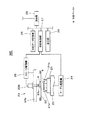
まず図1を参照して電子部品実装システムについて説明する。この電子部品実装システムは、複数の電子部品実装用装置である基板検査装置M1、印刷装置M2、印刷検査装置M3、塗布装置M4、電子部品搭載装置M5、搭載状態検査装置M6、リフロー装置M7
および実装状態検査装置M8の複数の電子部品実装用装置を連結して成る電子部品実装ライン1を通信ネットワーク2によって接続し、全体を管理コンピュータ3によって制御する構成となっている。
First, an electronic component mounting system will be described with reference to FIG. This electronic component mounting system includes a substrate inspection device M1, a printing device M2, a printing inspection device M3, a coating device M4, an electronic component mounting device M5, a mounting state inspection device M6, and a reflow device M7, which are a plurality of electronic component mounting devices.
In addition, an electronic
この電子部品実装システムによる電子部品実装方法においては、上面側の実装面4bに電極5が形成された基板4(図8(a)参照)に、半田粒子をフラックス成分に含有させた半田ペーストなどの接合材料によって電子部品を接合して実装基板を製造する。ここでは電子部品として,BGAなど平面視して矩形形状を有し、下面に接続用端子としてのバンプが複数形成されたバンプ付の電子部品8(図8参照)を基板4に半田接合により実装する例を示している。
In the electronic component mounting method by this electronic component mounting system, a solder paste in which solder particles are contained in a flux component on the substrate 4 (see FIG. 8A) on which the
基板検査装置M1は、基板4に形成された電極の検査を行う。印刷装置M2は、図8(b)に示すように、基板4に形成された電子部品接合用の電極5に半田ペースト6をスクリーン印刷により供給する。印刷検査装置M3は、印刷後の基板4における印刷状態を検査する。すなわち印刷装置M2によって供給された半田ペースト6の位置を検出して、この位置検出結果を半田ペースト(接合材料)位置データとして出力する。塗布装置M4は樹脂塗布部であり、図8(c)に示すように、半田ペースト6が印刷された後の基板4に、電子部品8が実装された状態において電子部品8を基板4に保持させる保持力を補強する補強樹脂7を塗布する。本実施の形態においては、矩形形状の電子部品8のコーナ部を補強対象部位とする例を示しており、補強樹脂7としてはエポキシ樹脂などの熱硬化性樹脂を主成分とするものが用いられる。
The substrate inspection apparatus M1 inspects the electrodes formed on the
電子部品搭載装置M5は、図8(d)に示すように、半田ペースト6が印刷されてさらに補強樹脂7が塗布された後の基板4に、下面にバンプ9が形成された電子部品8を搭載ヘッドによって搭載する。これにより、バンプ9が半田ペースト6を介して電極5の上面に着地するとともに、電子部品8の各コーナ部は予め基板4に塗布された補強樹脂7に接触する。搭載状態検査装置M6(第2の検査装置)は、部品搭載後の基板4上における電子部品8の有無や位置ずれを検査する。リフロー装置M7(半田接合手段)は部品搭載後の基板を加熱して、図8(e)に示すように、電子部品8を基板4に半田接合する。これにより、バンプ9は半田ペースト6が溶融固化した半田接合部6*を介して電極5に半田接合されるとともに、電子部品8のコーナ部において補強樹脂7が熱硬化した樹脂補強部7*によって電子部品8は基板4に保持される。実装状態検査装置M8(第3の検査装置)は、半田接合後の基板4上における電子部品8の実装状態を検査する。
As shown in FIG. 8D, the electronic component mounting apparatus M5 has the
次に各装置の構成について説明する。まず図2を参照して、基板検査装置M1、印刷検査装置M3、搭載状態検査装置M6および実装状態検査装置M8として用いられる検査装置について説明する。図2において、位置決めテーブル10上には基板保持部11が配置されており、基板保持部11には基板4が保持されている。基板保持部11の上方にはカメラ13が撮像方向を下向きにして配設されており、周囲に設けられた照明部12を点灯した状態で、カメラ13は基板4を撮像する。このとき、テーブル駆動部14を制御して位置決めテーブル10を駆動することにより、基板4の任意位置をカメラ13の直下に位置させて撮像することができる。
Next, the configuration of each device will be described. First, with reference to FIG. 2, an inspection apparatus used as the board inspection apparatus M1, the print inspection apparatus M3, the mounting state inspection apparatus M6, and the mounting state inspection apparatus M8 will be described. In FIG. 2, a
撮像によって取得した画像データは画像認識部17によって画像処理され、所定の認識結果が出力される。検査処理部16は、認識結果に基づいて検査対象項目ごとに合否判定を行うとともに、所定項目については検出値をフィードバックデータ、フィードフォワードデータとして出力する。出力されたデータは通信部18、通信ネットワーク2を介して、管理コンピュータ3や他装置に転送される。検査制御部15は、テーブル駆動部14、カメラ13、照明部12を制御することにより、検査動作を制御する。
Image data acquired by imaging is subjected to image processing by the
次に図3を参照して印刷装置M2の構成について説明する。図3において、位置決めテーブル20上には基板保持部21が配設されている。基板保持部21は基板4をクランパ21aによって両側から挟み込んで保持する。基板保持部21の上方には、マスクプレート22が配設されており、マスクプレート22には基板4の印刷部位に対応したパターン孔(図示せず)が設けられている。テーブル駆動部24によって位置決めテーブル20を駆動することにより、基板4はマスクプレート22に対して水平方向および垂直方向に相対移動する。
Next, the configuration of the printing apparatus M2 will be described with reference to FIG. In FIG. 3, a
マスクプレート22の上方にはスキージ部23が配置されている。スキージ部23は、スキージ23cをマスクプレート22に対して昇降させるとともにマスクプレート22に対して所定押圧力(印圧)で押し付ける昇降押圧機構23b、スキージ23cを水平移動させるスキージ移動機構23aより成る。昇降押圧機構23b、スキージ移動機構23aは、スキージ駆動部25により駆動される。基板4をマスクプレート22の下面に当接させた状態で、半田ペースト6が供給されたマスクプレート22の表面に沿ってスキージ23cを所定速度で水平移動させることにより、半田ペースト6は図示しないパターン孔を介して基板4の上面に印刷される。
A
この印刷動作は、テーブル駆動部24、スキージ駆動部25を印刷制御部27によって制御することによって行われる。この制御に際しては、印刷データ記憶部26に記憶された印刷データに基づいて、スキージ23cの動作や基板4とマスクプレート22との位置合わせが制御される。表示部29は印刷装置の稼動状態を示す各種の指標データや、印刷動作状態の異常を示す異常報知を表示する。通信部28は通信ネットワーク2を介して管理コンピュータ3や電子部品実装ライン1を構成する他装置との間でのデータ授受を行う。
This printing operation is performed by controlling the
次に図4を参照して塗布装置M4の構成について説明する。図4において位置決めテーブル30上には基板保持部31が配設されており、基板保持部31は印刷検査装置M3から搬送された基板4を保持する。基板保持部31の上方には、ヘッド駆動機構33によって移動する塗布ヘッド32が配設されている。塗布ヘッド32には補強樹脂7を貯留するシリンジ32aが昇降自在に装着されている。シリンジ32aは下端部に塗布ノズル32bを備えており、シリンジ32aを基板4の塗布対象部位に下降させて塗布ノズル32bから補強樹脂7を吐出することにより、基板4における塗布対象部位(搭載後の電子部品8のコーナ部に相当する部位)には、補強樹脂7が塗布される。
Next, the configuration of the coating apparatus M4 will be described with reference to FIG. In FIG. 4, a
補強樹脂7は前述のように熱硬化性樹脂を主成分としており、リフロー装置M7による加熱工程において熱硬化する。本実施の形態にて用いられる補強樹脂7としては、半田ペースト6が加熱によって溶融した状態において未だ熱硬化が完了せずに流動性を有しているような特性のものが選定される。これにより、半田ペースト6が溶融固化するリフロー過程において、電子部品8が補強樹脂7に接触した状態にあっても、補強樹脂7の流動性により電子部品8の水平方向の移動が許容される。したがって半田ペースト6中の半田成分が溶融した溶融半田の表面張力によって、電子部品8のバンプ9の電極5に対する相対的な位置ずれを補正するセルフアライメント作用を阻害しないようになっている。このような特性を有する補強樹脂は、電子部品用接着剤として既に公知である(例えば特開2005−26502号公報参照)。
The reinforcing
ヘッド駆動機構33、位置決めテーブル30はそれぞれ塗布ヘッド駆動部35、テーブル駆動部34によって駆動される。前記塗布動作において、塗布データ記憶部36に記憶された塗布データ、すなわち基板4における塗布対象部位の平面位置を示す塗布座標に基づいて、塗布制御部37によってテーブル駆動部34、塗布ヘッド駆動部35を制御することにより、塗布ヘッド32による基板4への補強樹脂の塗布位置を制御することができ
る。すなわち、塗布制御部37からの制御指令値が、塗布位置を制御する制御パラメータとなっている。表示部39は塗布装置M4の各種の稼動状態を表す指標データや塗布動作状態の異常を示す異常報知を表示する。通信部38は通信ネットワーク2を介して管理コンピュータ3や電子部品実装ライン1を構成する他装置との間でデータ授受を行う。
The
次に図5を参照して電子部品搭載装置M5の構成について説明する。図5において位置決めテーブル40上には基板保持部41が配設されており、基板保持部41は塗布装置M4から搬送された基板4を保持する。基板保持部41の上方には、ヘッド駆動機構43によって移動する搭載ヘッド42が配設されている。搭載ヘッド42は電子部品を吸着するノズル42aを備えており、搭載ヘッド42は部品供給部(図示省略)から電子部品8をノズル42aによって吸着保持して取り出す。そして搭載ヘッド42を基板4上に移動させて、基板4に対して下降させることにより、ノズル42aに保持した電子部品を基板4に搭載する。
Next, the configuration of the electronic component mounting apparatus M5 will be described with reference to FIG. In FIG. 5, a
ヘッド駆動機構43、位置決めテーブル40はそれぞれ搭載ヘッド駆動部45、テーブル駆動部44によって駆動される。前記搭載動作において、搭載データ記憶部46に記憶された搭載データ、すなわち基板4上での電子部品の実装座標に基づいて、搭載制御部47によってテーブル駆動部44、搭載ヘッド駆動部45を制御することにより、搭載ヘッド42による基板4への電子部品搭載位置を制御することができる。すなわち、搭載制御部47からの制御指令値が、搭載位置を制御する制御パラメータとなっている。表示部49は電子部品搭載装置M5の各種の稼動状態を表す指標データや搭載動作状態の異常を示す異常報知を表示する。通信部48は通信ネットワーク2を介して管理コンピュータ3や電子部品実装ライン1を構成する他装置との間でデータ授受を行う。
The
次に図6を参照してリフロー装置M7の構成について説明する。図6において、基台50上に設けられた加熱室52内には、基板4を搬送する搬送路51が水平に配設されている。加熱室52内は複数の加熱ゾーンに仕切られており、各加熱ゾーンは、それぞれ温調機能を有する加熱手段53を備えている。加熱手段53を駆動して各加熱ゾーンを所定の温度条件に加熱した状態で、半田ペースト6上に電子部品8が搭載された基板4を上流側から順次加熱ゾーンを通過させることにより、半田ペースト6中の半田成分が加熱溶融する。これにより電子部品8は基板4に半田接合される。
Next, the configuration of the reflow apparatus M7 will be described with reference to FIG. In FIG. 6, a
このリフロー過程において、加熱データ記憶部56に記憶された加熱データ、すなわちリフロー過程における温度プロファイルを実現するための制御パラメータである温度指令値に基づいて加熱制御部57によって各加熱手段53を制御することにより、所望の温度プロファイルが設定される。表示部59はリフロー装置M7の稼動状態を表す指標データや、所定の温度条件からの偏差が許容範囲を超え加熱動作状態が異常であることを示す異常報知を表示する。通信部58は通信ネットワーク2を介して管理コンピュータ3や電子部品実装ライン1を構成する他装置との間でデータ授受を行う。
In this reflow process, each heating means 53 is controlled by the
次に図7を参照して電子部品実装システムの制御系の構成について説明する。ここでは、電子部品実装過程における品質管理を目的としたデータ授受機能を説明する。図7において、全体制御部60(全体制御手段)は管理コンピュータ3によって実行される制御処理範囲のうちの品質管理機能を担うものであり、通信ネットワーク2を介して電子部品実装ラインを構成する各装置から転送されるデータを受信し、予め定められた判定アルゴリズムに基づいて必要な判定処理を行い、処理結果を各装置に指令データとして通信ネットワーク2を介して出力する。
Next, the configuration of the control system of the electronic component mounting system will be described with reference to FIG. Here, a data transfer function for the purpose of quality control in the electronic component mounting process will be described. In FIG. 7, the overall control unit 60 (overall control means) is responsible for the quality management function in the control processing range executed by the
すなわち図2に示す検査装置を用いた基板検査装置M1、印刷検査装置M3、搭載状態検査装置M6および実装状態検査装置M8にそれぞれ備えられた基板検査処理部16A、
印刷検査処理部16B、搭載状態検査処理部16Cおよび実装状態検査処理部16Dは、それぞれ通信部18A、18B、18Cおよび18Dを介して通信ネットワーク2に接続されている。また印刷装置M2、塗布装置M4、電子部品搭載装置M5およびリフロー装置M7に備えられた各部(図3、図4、図5、図6参照)は、それぞれ通信部28、38、48、58を介して通信ネットワーク2と接続されている。
That is, the board
The print
これにより、いずれかの検査工程において抽出されたデータに基づいて上流側装置の制御パラメータを修正・更新するフィードバック処理や、下流側装置の制御パラメータを修正、更新するフィードフォワード処理が、各装置の稼動中に随時可能な構成となっている。 As a result, feedback processing for correcting / updating the control parameters of the upstream device based on data extracted in one of the inspection processes and feedforward processing for correcting and updating the control parameters of the downstream device are performed by each device. The configuration is possible at any time during operation.
この電子部品実装システムは上記の様に構成されており、以下電子部品実装方法および実装過程において行われるキャリブレーション、すなわち制御パラメータの修正・更新処理について説明する。まず図示しない基板供給部から供給される基板4は、基板検査装置M1(図2参照)に搬入される。ここで基板4をカメラ13によって撮像して画像認識することにより、図9(a)に示すように基板4に形成された各電極5が認識される。ここでは、1つの電子部品8の各バンプ9に対応する複数の電極5を部品単位で括った電極群105を1つの認識対象とする例を示している。これにより、電極群105毎に各電極5(図10(a)に示す(1)〜(9)参照)の重心位置を示す位置データ(電極位置データ)が、基板4の認識マーク4aを基準とした座標値xL(i),yL(i)として求められ、基板検査処理部16Aに送られる。
This electronic component mounting system is configured as described above. Hereinafter, calibration performed in the electronic component mounting method and the mounting process, that is, control parameter correction / update processing will be described. First, the
基板検査処理部16Aは各電極5ごとに求められた複数の座標値に基づいて検査処理を行う。すなわち求められた座標値を統計処理することにより、当該基板4が使用可能か否かの合否判断を行うとともに、電極群105毎に電極5の位置ずれ傾向を判断する。そして図10(a)に示すように、実際の電極位置の設計データ上の正規位置に対する位置ずれ量が、許容範囲のばらつき範囲内で特定方向に偏っている場合には、この偏りを示す偏差Δ1を電極群105毎に数値データ(X方向偏差成分Δ1(x)、Y方向偏差成分Δ1(y))として求める。
The substrate
そして下流側装置においてこの偏差分だけ制御パラメータを修正するフィードフォワード処理を行う。このフィードフォワード処理のための偏差データは、通信部18Aを介して通信ネットワーク2に転送され、全体制御部60によって下流側の印刷装置M2、塗布装置M4、電子部品搭載装置M5に対して補正指令値として出力される。なお、ここでは電極位置データの統計処理の方法として、電極5を部品単位で括った電極群105を1つの対象とする例を示しているが、基板4全体の電極5を対象として統計処理を行うようにしてもよい。
Then, in the downstream apparatus, a feedforward process for correcting the control parameter by this deviation is performed. Deviation data for this feedforward process is transferred to the
次に、基板4は印刷装置M2に搬入されて基板保持部21に保持され、この基板4に対して半田ペースト6が印刷される。このとき、上述のフィードフォワード処理によって印刷データ記憶部26には電極位置の偏差データに基づく補正指令値が記憶されており、位置決めテーブル20を駆動して基板4をマスクプレート22に対して位置合わせする際には、この補正指令値に基づいて位置決めテーブル20の移動量が補正される。これにより、電極5が基板4の認識マーク4aに対する正規位置から位置ずれを生じている場合にあっても、印刷装置M2においては電極5上の正しい位置に半田ペースト6が印刷される。
Next, the
次に、半田ペースト印刷後の基板4は印刷検査装置M3に搬入される。ここでは、同様の検査装置によって、図9(b)に示すように各電極5ごとに、電極5上に印刷された半田ペースト6の重心位置を示す位置データ(半田位置データ)が、認識マーク4aを基準とした座標値xS(i),yS(i)として画像認識によって求められる。ここでも同様
に1つの電子部品8の各バンプ9に対応して印刷された複数の半田ペースト6を部品単位で括った印刷半田群106を1つの認識対象とする例を示している。そして認識結果は印刷検査処理部16Bによって同様に検査処理され、印刷結果の合否判断および印刷位置の位置ずれ傾向が判断される。そして図10(b)に示すように、正規位置に対する位置ずれ量の偏差Δ2を印刷半田群106毎に数値データ(X方向偏差成分Δ2(x)、Y方向偏差成分Δ2(y))として求める。
Next, the
ここで印刷検査によって得られた偏差データは、フィードバック処理およびフィードフォワード処理の双方に用いられる。すなわち、印刷装置M2において当該基板4への印刷動作に用いられた制御パラメータと、検査によって検出された印刷位置とを比較することにより、印刷装置M2に起因して生じた位置ずれを求めることができる。そしてこの位置ずれ分だけ印刷装置M2の制御パラメータを修正するキャリブレーションを行うことにより、印刷動作における位置ずれ量を減少させることができる。また印刷位置の偏差データは、下流側の塗布装置M4および電子部品搭載装置M5にフィードフォワードされる。
Here, the deviation data obtained by the print inspection is used for both feedback processing and feedforward processing. That is, the positional deviation caused by the printing apparatus M2 can be obtained by comparing the control parameter used for the printing operation on the
さらに、各電極5上に印刷された半田ペーストの撮像データに基づいて、各電極部位ごとに半田部分(図9(b)に示す電極5上のハッチング部分)の面積を演算することにより、各電極部位ごとの半田印刷量が検出される。そして検出された半田印刷量が許容範囲を超えてばらついている場合には、印刷条件の設定が不良であると判定され、その旨表示される。印刷条件には、スキージ23cをマスクプレート22上で移動させるスキージ速度やスキージ23cをマスクプレート22に押し付ける印圧値、さらにはスキージング後に基板4をマスクプレート22の下面から引き離す版離れ速度などがあり、これらの印刷動作制御上の数値データが、制御パラメータとして設定される。
Further, based on the imaging data of the solder paste printed on each
次に、半田印刷後の基板4は、塗布装置M4に搬入され、補強樹脂7の塗布が行われる。すなわち、図11(a)に示すように、1つの電子部品8に対応した複数の電極5より構成される電極群105の各コーナ位置には、補強樹脂7A,7B,7C,7Dが塗布される。このとき、電極5は平均的にΔ1x、Δ1yだけ正規位置に対して位置ずれしており、半田ペースト6は平均的にΔ2x、Δ2yだけ正規位置に対して位置ずれしている。したがって、半田ペースト6は電極5に対してΔ2x−Δ1x、Δ2y−Δ1yだけ相対的に位置ずれした状態となっている。なお、ここでは、位置ずれ方向が、正規位置に対してX方向(−)側、Y方向(−)側である例を示している。
Next, the
このような位置ずれ状態の電極群105に対して補強樹脂7を塗布する際には、補強樹脂7A,7B,7C,7DをそれぞれΔ2x、Δ2yだけ、正規位置に対してX方向(−)側、Y方向(−)側にずらすように位置補正する(矢印a)。すなわち塗布後の補強樹脂7A,7B,7C,7Dと直近のコーナ部の電極5に印刷された半田ペースト6の端部とのX方向、Y方向の間隔x1,y1が、ほぼ等しくなるように、テーブル駆動部34および塗布ヘッド駆動部35に指令される制御パラメータを補正する。
When applying the reinforcing
これにより、印刷された半田ペースト6が正規位置に対して位置ずれを生じた状態において、補強樹脂7を正規位置に塗布した場合に生じる可能性のある不具合、すなわち先に印刷された半田ペースト6に後から塗布された補強樹脂7が接触して部分的に混合することに起因する半田ペースト6の半田接合性の低下などの不具合を防止することができる。なお補強樹脂7の塗布位置の補正においては、塗布された補強樹脂7A,7B,7C,7Dが、コーナ部に位置する電極5に重ならないよう、データ上で確認した上で位置補正量を設定する。すなわち上述例において、Δ2x、Δ2yだけそのまま位置補正すると、補強樹脂7A,7B,7C,7Dのいずれかが電極5と重なる場合には、位置補正量を電極5との相対位置との兼ね合いで再設定する。
As a result, in a state where the printed
次に半田印刷後に補強樹脂7が塗布された基板4は、電子部品搭載装置M5に搬入され、ここで部品搭載作業が実行される。すなわち部品供給部から搭載ヘッド42によって電子部品8を取り出し、電極5上に半田ペースト6を介してバンプ9を着地させるとともに、電子部品8のコーナ部を、基板4上に予め先塗りされた補強樹脂7に接触させる。このとき、搭載ヘッド42によって基板4に電子部品を搭載する際には、テーブル駆動部44および搭載ヘッド駆動部45に指令される制御パラメータを、フィードフォワードされた偏差Δ2x、Δ2yだけ補正した上で搭載動作を行う。これにより、半田ペースト6の印刷位置が全体的に偏っている場合においても、図11(b)に示すように、電子部品8のバンプ9は印刷された半田ペースト6に対して位置ずれを生じることなく搭載される。この状態においては、バンプ9は電極5に対しては、位置ずれを生じている。
Next, the
次に、電子部品が搭載された基板4は搭載状態検査装置M6に搬送され、ここで電子部品の搭載状態を検査するための外観検査が行われる。すなわち図9(c)に示すように、基板4上の各電子部品8(i)ごとに、電子部品8の重心位置を示す位置データ(部品位置データ)を、認識マーク4aを基準とした座標値xP(i),yP(i)として求める。そして認識結果は搭載状態検査処理部16Cによって検査処理され、搭載状態の合否判断および搭載位置の位置ずれ傾向が判断される。すなわち図10(c)に示すように、正規位置に対する位置ずれ量の偏差Δ3が電子部品8毎に数値データ(X方向偏差成分Δ3(x)、Y方向偏差成分Δ3(y))として求められる。そしてこの偏差データは同様に通信ネットワーク2に転送される。ここでは、搭載位置の偏差データは電子部品搭載装置M5にフィードバックされ、偏差Δ3だけ制御パラメータを修正するキャリブレーションが行われる。また、電極5上に電子部品8が搭載されていない場合や、搭載されていても正常な姿勢でなく立ち姿勢となっている場合や、回転方向が大きくずれているような場合には、画像認識時にその状態が検出され、搭載動作状態の異常と判定されてその旨表示される。
Next, the
この後、電子部品が搭載された基板4はリフロー装置M7に搬入され、ここで所定の温度プロファイルに従って基板4を加熱することにより、半田ペースト6中の半田成分が溶融し、これにより、バンプ9は半田ペースト6が溶融固化した半田接合部6*を介して電極5に半田接合されるとともに、補強樹脂7が熱硬化した樹脂補強部7*によって電子部品8はコーナ部において基板4に保持される。
Thereafter, the
このリフロー過程において、電子部品8の各バンプ9は、図11(b)に示す状態では位置ずれしている場合にあっても、半田ペースト6中の半田成分が溶融した溶融半田が表面張力により電極5の上面の全範囲に亘って濡れ広がることにより、バンプ9を電極5の上面に均一に位置合わせしようとするセルフアライメント作用が働く。この結果、各バンプ9は図11(c)に示すように、それぞれ電極5のほぼ中心に正しく位置合わせされた状態で、半田接合部6*を介して電極5に半田接合される。
In this reflow process, even if each
このとき、補強樹脂7は前述のように半田ペースト6中の半田成分が溶融した状態では未だ熱硬化が完了せずに流動性を有しているため、上述のセルフアライメント効果を阻害することなく、電子部品8の各コーナ部は補強樹脂7A,7B,7C,7Dに対して水平方向に相対移動する。すなわちセルフアライメント後の補強樹脂7A,7B,7C,7Dの電子部品8の各コーナ部に対する相対位置は、コーナ部によって幾分異なったものとなるが、その相違量は僅かであり、補強樹脂7A,7B,7C,7Dが熱硬化して形成された樹脂補強部7A*,7B*,7C*,7D*による補強効果を阻害することはない。
At this time, since the reinforcing
なお、図11(a)に示す例においては、電子部品8の各コーナ部に対応する補強樹脂7A,7B,7C,7Dを一律に同一方向、同一補正量で位置補正する例を示しているが、補強樹脂7の塗布位置を位置補正する目的を鑑みれば、補強樹脂7A,7B,7C,7
Dを必ずしも一律に位置補正する必要はない。すなわち、位置補正の目的は、既に印刷された半田ペースト6と塗布される補強樹脂7の重なりを防ぐことであり、正規位置に塗布しても半田ペースト6と補強樹脂7の重なりが生じないコーナ部については補強樹脂7の塗布位置を補正する必要はない。
In the example shown in FIG. 11A, the position of the reinforcing
It is not always necessary to correct the position of D uniformly. That is, the purpose of the position correction is to prevent the already printed
例えば、図12(a)に示すように、半田ペースト6がX方向,Y方向についていずれも(−)側に位置ずれしているような場合には、右上のコーナ部に近接する補強樹脂7Aはそのまま塗布しても、半田ペースト6と補強樹脂7の重なりが生じないことから、正規位置に塗布すればよい。これに対し、補強樹脂7Bについては、半田ペースト6がY方向の(−)側に位置ずれしていることから、Y方向の(−)側(矢印b)についてのみ位置補正する。また、補強樹脂7Dについては、半田ペースト6がX方向の(−)側に位置ずれしていることから、X方向の(−)側(矢印d)についてのみ位置補正する。
For example, as shown in FIG. 12A, when the
そして補強樹脂7Cについては、半田ペースト6がX方向、Y方向の双方について(−)側に位置ずれしていることから、X方向,Y方向の双方について(−)側(矢印c)に位置補正する。すなわち、図12(a)に示す例では、既に印刷された半田ペースト6と塗布される補強樹脂7の重なりを防ぐという目的を達成する上で必要なコーナ部についてのみ位置補正を行い、補強樹脂7の塗布位置補正を必要最小限に抑える例を示している。印刷検査装置M3によって検出した接合材料位置データに基づいて塗布装置M4を制御する制御パラメータを更新する際には、半田ペースト6、補強樹脂7の近接が許容される度合いや、位置ずれが発生する傾向に応じて、予め補正目的に即した適正な更新パターンを設定しておくことが望ましい。
With respect to the reinforcing
次いで補強樹脂7が塗布された基板4に対して、図11(b)に示す例と同様に、電子部品8の搭載が実行される。このとき、電子部品8のバンプ9が半田ペースト6に対して位置ずれを生じないように位置補正した上で、電子部品8の位置補正が行われる。そしてこの後、基板4はリフロー装置M7に搬入され、図11(c)に示す例と同様に、バンプ9を半田ペースト6が溶融固化した半田接合部6*を介して電極5に半田接合するとともに、補強樹脂7が熱硬化した樹脂補強部7*によって電子部品8を基板4に保持させる。このとき、電子部品8の各バンプ9は、同様に溶融半田のセルフアライメント作用によって、図12(c)に示すように、それぞれ電極5に正しく位置合わせされた状態で、半田接合部6*を介して電極5に半田接合される。
Next, as in the example shown in FIG. 11B, the
このとき、位置補正の目的を達成する上で補強樹脂7の塗布位置の補正を必要最小限に抑えるようにしていることから、電子部品8の各コーナ部が補強樹脂7A,7B,7C,7Dに対して水平方向に位置ずれする度合いは、図11(c)に示す例と比較して、より小さくなっている。したがって、補強樹脂7A,7B,7C,7Dが熱硬化して形成された樹脂補強部7A*,7B*,7C*,7D*による補強効果を阻害することなく、位置補正の目的を達成することが可能となっている。
At this time, since the correction of the application position of the reinforcing
リフロー後の基板4は、実装状態検査装置M8に搬入され、ここで最終的な電子部品8の実装状態が検査される。すなわち外観検査によって電子部品8の有無や姿勢・位置の異常の有無が検査される。ここで検出される項目のうち、リフロー過程における加熱状態の不良に起因するものについては、リフロー装置M7にフィードバックされ、加熱データ記憶部56の制御パラメータの修正が行われる。
The
上記説明したように、本実施の形態に示す電子部品実装方法は、印刷装置M2によって基板4に形成された電子部品接合用の電極5に接合材料である半田ペースト6を供給する接合材料供給工程と、接合材料供給工程において供給された半田ペースト6の位置を、印刷検査装置M3によって検出して、この位置検出結果を接合材料位置データとして出力す
る接合材料位置検出工程と、さらに接合材料位置検出工程後の基板4に、電子部品8が実装された状態においてこの電子部品8を基板4に保持させる保持力を補強する補強樹脂7を、樹脂塗布部としての塗布装置M4によって塗布する樹脂塗布工程と、電子部品搭載装置M5の搭載ヘッド42によって部品供給部から電子部品8を取り出し、半田ペースト6が供給されてさらに補強樹脂7が塗布された基板4に搭載する搭載工程と、半田接合手段としてのリフロー装置M7によって基板4を加熱することにより、搭載された電子部品8を半田ペースト6によって基板4に接合するとともに、補強樹脂7を熱硬化させて電子部品8を基板4に保持させる加熱工程とを含んだ形態となっている。
As described above, in the electronic component mounting method shown in the present embodiment, the bonding material supply step of supplying the
そして樹脂塗布工程において、接合材料位置検出工程において出力された接合材料位置データに基づいて、塗布装置M4を制御する制御パラメータを更新するようにしている。これにより、接合材料である半田ペースト6と併せて補強樹脂7を用いる実装形態において、半田ペースト6と補強樹脂7との混合を防止して、実装品質を確保することができる。
In the resin coating process, control parameters for controlling the coating apparatus M4 are updated based on the bonding material position data output in the bonding material position detection process. Thereby, in the mounting form using the reinforcing
なお上記実施の形態においては、補強樹脂7が下面にバンプ9が設けられた電子部品8のコーナ部を補強する場合について本発明を適用した例を示しているが、両端部に接続端子を有するチップ型部品など、矩形小型部品の中央部を接着剤によって固定するために補強樹脂7が塗布される場合についても、本発明を適用することができる。すなわち、この場合においても接続端子に対応する電極上に印刷された半田ペースト6の位置ずれ状態に応じて補強樹脂の塗布位置を補正することにより、半田ペースト6と補強樹脂7との混合を防止することができる。
In the above embodiment, the example in which the present invention is applied to the case where the reinforcing
また上記実施の形態では、図1に示すように、複数の電子部品実装用装置を直列に配列した電子部品実装ライン1によって電子部品実装システムを構成した例を示しているが、本発明の部品実装システムの構成例は図1に示す実施例には限定されず、多様なバリエーションが設定可能である。例えば、図13に示す電子部品実装ライン1Aのように、印刷装置M2の下流側からリフロー装置M7の上流側までを構成する電子部品実装用装置を、中央部にライン方向に配設された基板搬送機構70の両側部に作業機構を配設した構成としてもよい。ここでは、印刷検査装置M3、塗布装置M4を基板搬送機構70を夾んで対向配置し、さらに電子部品搭載装置M5、搭載状態検査装置M6を基板搬送機構70を夾んで対向配置した構成例を示している。もちろん、請求項1に示す工程順序を実現可能な設備構成であれば、図13に示す構成例以外の設備構成であっても、本発明を適用することが可能である。
In the above embodiment, as shown in FIG. 1, an example in which an electronic component mounting system is configured by an electronic
本発明の電子部品実装方法は、接合材料と併せて補強樹脂を用いる実装形態において、接合材料と補強樹脂との混合を防止して、実装品質を確保することができるという効果を有し、基板に電子部品を半田ペーストなどの接合材料によって接合して実装基板を製造する分野において有用である。 The electronic component mounting method of the present invention has an effect of preventing the mixing of the bonding material and the reinforcing resin in the mounting form using the reinforcing resin together with the bonding material, thereby ensuring the mounting quality, and the substrate. It is useful in the field of manufacturing a mounting substrate by bonding electronic components to each other with a bonding material such as solder paste.
1 電子部品実装ライン
2 通信ネットワーク
3 管理コンピュータ
4 基板
5 電極
6 半田ペースト(接合材料)
7 補強樹脂
8 電子部品
M1 基板検査装置
M2 印刷装置
M3 印刷検査装置
M4 塗布装置(樹脂塗布部)
M5 電子部品搭載装置
M6 搭載状態検査装置
M7 リフロー装置(半田接合手段)
M8 実装状態検査装置
DESCRIPTION OF
7 Reinforcing
M5 Electronic component mounting device M6 Mounting state inspection device M7 Reflow device (solder bonding means)
M8 mounting state inspection device
Claims (3)
印刷装置によって前記基板に形成された電子部品接合用の電極に前記接合材料を供給する接合材料供給工程と、前記接合材料供給工程において供給された接合材料の位置を印刷検査装置によって検出して、この位置検出結果を接合材料位置データとして出力する接合材料位置検出工程と、前記接合材料位置検出工程後の前記基板に、前記電子部品が実装された状態においてこの電子部品を前記基板に保持させる保持力を補強する補強樹脂を、樹脂塗布部によって塗布する樹脂塗布工程と、
搭載ヘッドによって部品供給部から前記電子部品を取り出し、前記接合材料が供給されてさらに前記補強樹脂が塗布された前記基板に搭載する搭載工程と、半田接合手段によって前記基板を加熱することにより、前記搭載された電子部品を前記接合材料によって前記基板に接合するとともに、前記補強樹脂を熱硬化させて前記電子部品を基板に保持させる加熱工程とを含み、
前記樹脂塗布工程において、前記接合材料位置データに基づいて前記樹脂塗布部を制御する制御パラメータを更新することにより、
前記接合材料が供給されるべき正規位置に対して位置ずれして前記電極に供給された基板に対して前記補強樹脂を塗布する際、前記補強樹脂が塗布されるべき正規位置に対して前記接合材料の位置ずれ量に基づいて前記補強樹脂の塗布位置を補正することを特徴とする電子部品実装方法。 An electronic component mounting method for manufacturing a mounting substrate by bonding an electronic component to a substrate with a bonding material by an electronic component mounting system composed of a plurality of electronic component mounting apparatuses,
A bonding material supply step of supplying the bonding material to an electrode for bonding electronic components formed on the substrate by the printing device; and a position of the bonding material supplied in the bonding material supply step is detected by a printing inspection device; A bonding material position detecting step for outputting the position detection result as bonding material position data, and a holding for holding the electronic component on the substrate in a state where the electronic component is mounted on the substrate after the bonding material position detecting step. A resin application step of applying a reinforcing resin to reinforce the force by a resin application part;
By taking out the electronic component from the component supply unit by a mounting head, mounting the substrate on the substrate to which the bonding material is supplied and further applying the reinforcing resin, and heating the substrate by solder bonding means, A heating step of bonding the mounted electronic component to the substrate with the bonding material, and thermosetting the reinforcing resin to hold the electronic component on the substrate,
In the resin application step, by updating a control parameter for controlling the resin application part based on the bonding material position data ,
When the reinforcing resin is applied to the substrate supplied to the electrodes with a displacement from the normal position where the bonding material is to be supplied, the bonding is performed with respect to the normal position where the reinforcing resin is to be applied. An electronic component mounting method, wherein the application position of the reinforcing resin is corrected based on a positional deviation amount of the material .
Priority Applications (3)
| Application Number | Priority Date | Filing Date | Title |
|---|---|---|---|
| JP2009100520A JP4883131B2 (en) | 2009-04-17 | 2009-04-17 | Electronic component mounting method |
| US12/761,578 US20100264196A1 (en) | 2009-04-17 | 2010-04-16 | Electronic component mounting method |
| CN201010164722.2A CN101868126B (en) | 2009-04-17 | 2010-04-19 | Electronic component mounting method |
Applications Claiming Priority (1)
| Application Number | Priority Date | Filing Date | Title |
|---|---|---|---|
| JP2009100520A JP4883131B2 (en) | 2009-04-17 | 2009-04-17 | Electronic component mounting method |
Publications (2)
| Publication Number | Publication Date |
|---|---|
| JP2010251579A JP2010251579A (en) | 2010-11-04 |
| JP4883131B2 true JP4883131B2 (en) | 2012-02-22 |
Family
ID=42959618
Family Applications (1)
| Application Number | Title | Priority Date | Filing Date |
|---|---|---|---|
| JP2009100520A Active JP4883131B2 (en) | 2009-04-17 | 2009-04-17 | Electronic component mounting method |
Country Status (3)
| Country | Link |
|---|---|
| US (1) | US20100264196A1 (en) |
| JP (1) | JP4883131B2 (en) |
| CN (1) | CN101868126B (en) |
Families Citing this family (15)
| Publication number | Priority date | Publication date | Assignee | Title |
|---|---|---|---|---|
| JP5482605B2 (en) * | 2010-09-27 | 2014-05-07 | パナソニック株式会社 | Electronic component mounting method |
| JP2012199476A (en) * | 2011-03-23 | 2012-10-18 | Panasonic Corp | Adhesive coating device |
| US9439335B2 (en) | 2011-12-08 | 2016-09-06 | Panasonic Intellectual Property Management Co., Ltd. | Electronic component mounting line and electronic component mounting method |
| JP5603496B2 (en) * | 2011-12-08 | 2014-10-08 | パナソニック株式会社 | Electronic component mounting line and electronic component mounting method |
| WO2013094098A1 (en) * | 2011-12-22 | 2013-06-27 | パナソニック株式会社 | Electronic component mounting line and electronic component mounting method |
| JP6135892B2 (en) * | 2012-01-25 | 2017-05-31 | パナソニックIpマネジメント株式会社 | Electronic component mounting method and electronic component mounting line |
| JP5963129B2 (en) * | 2012-02-03 | 2016-08-03 | Jukiオートメーションシステムズ株式会社 | Print inspection apparatus, print inspection system, inspection data statistical method, program, and substrate manufacturing method |
| JP6450923B2 (en) * | 2013-12-20 | 2019-01-16 | パナソニックIpマネジメント株式会社 | Electronic component mounting system, electronic component mounting method, and electronic component mounting apparatus |
| US20150373845A1 (en) * | 2014-06-24 | 2015-12-24 | Panasonic Intellectual Property Management Co., Ltd. | Electronic component mounting structure and method of manufacturing electronic component mounting structure |
| EP3223594B1 (en) | 2014-11-20 | 2021-03-24 | Koh Young Technology Inc. | Component inspection apparatus and component mounting system having same |
| JP6535755B2 (en) * | 2015-04-15 | 2019-06-26 | エクスロン インターナショナル ゲゼルシャフト ミット ベシュレンクテル ハフツングYxlon International Gmbh | How to test electronic components |
| JP6915981B2 (en) * | 2016-11-17 | 2021-08-11 | ハンファ精密機械株式会社 | Electronic component mounting system and electronic component mounting method |
| US11477927B2 (en) * | 2017-02-20 | 2022-10-18 | Fuji Corporation | Component mounting system and component mounting method |
| CN106658987A (en) * | 2017-02-28 | 2017-05-10 | 深圳天珑无线科技有限公司 | Part surface mount position adjustment method and part surface mount position detection method and device |
| CN108882550A (en) * | 2018-08-27 | 2018-11-23 | 郑州云海信息技术有限公司 | A method of it improving PCBA and manufactures AOI yield |
Family Cites Families (8)
| Publication number | Priority date | Publication date | Assignee | Title |
|---|---|---|---|---|
| US5573602A (en) * | 1994-12-19 | 1996-11-12 | Motorola, Inc. | Solder paste |
| JP3552422B2 (en) * | 1996-10-04 | 2004-08-11 | 株式会社デンソー | Ball grid array semiconductor device and its mounting method |
| JPH11220250A (en) * | 1998-02-02 | 1999-08-10 | Matsushita Electric Ind Co Ltd | Application method and device of electronic component adhesive material |
| DE10152408A1 (en) * | 2000-10-25 | 2002-05-16 | Matsushita Electric Ind Co Ltd | System for automatic mounting of electronic components onto a circuit board uses camera scanning of board |
| JP2002271014A (en) * | 2001-03-09 | 2002-09-20 | Hitachi Kokusai Electric Inc | Method of mounting electronic component |
| JP4413543B2 (en) * | 2003-07-03 | 2010-02-10 | パナソニック株式会社 | Electronic component adhesive and electronic component mounting method |
| JP4381795B2 (en) * | 2003-12-19 | 2009-12-09 | パナソニック株式会社 | Electronic component mounting method |
| JP2007287779A (en) * | 2006-04-13 | 2007-11-01 | Matsushita Electric Ind Co Ltd | System and method for mounting electronic component, and mounted state inspection apparatus |
-
2009
- 2009-04-17 JP JP2009100520A patent/JP4883131B2/en active Active
-
2010
- 2010-04-16 US US12/761,578 patent/US20100264196A1/en not_active Abandoned
- 2010-04-19 CN CN201010164722.2A patent/CN101868126B/en active Active
Also Published As
| Publication number | Publication date |
|---|---|
| CN101868126B (en) | 2014-10-08 |
| US20100264196A1 (en) | 2010-10-21 |
| JP2010251579A (en) | 2010-11-04 |
| CN101868126A (en) | 2010-10-20 |
Similar Documents
| Publication | Publication Date | Title |
|---|---|---|
| JP4883131B2 (en) | Electronic component mounting method | |
| KR101292635B1 (en) | Electronic component mounting system and electronic component mounting method | |
| KR101260429B1 (en) | Electronic component mounting system, electronic component mounting device and electronic component mounting method | |
| WO2014076968A1 (en) | Electronic component mounting system | |
| JP4367524B2 (en) | Electronic component mounting system and electronic component mounting method | |
| JP4289381B2 (en) | Electronic component mounting system and electronic component mounting method | |
| JP2007287779A (en) | System and method for mounting electronic component, and mounted state inspection apparatus | |
| JP3685035B2 (en) | Electronic component mounting system and electronic component mounting method | |
| US20150163969A1 (en) | Electronic component mounting system and electronic component mounting method | |
| CN104798456A (en) | Electronic-component-mounting system and electronic-component mounting method | |
| JP3873757B2 (en) | Electronic component mounting system and electronic component mounting method | |
| JP2008199070A (en) | Method for mounting electronic component | |
| JP4595857B2 (en) | Electronic component mounting system and electronic component mounting method | |
| JP5927431B2 (en) | Component mounting apparatus and component mounting method | |
| JP4541216B2 (en) | Electronic component mounting method | |
| JP2014041892A (en) | Screen printing system and screen printing method | |
| JP5990775B2 (en) | Electronic component mounting system, electronic component mounting apparatus, and electronic component mounting method | |
| JP4702237B2 (en) | Electronic component mounting apparatus and electronic component mounting method | |
| JP4743059B2 (en) | Electronic component mounting system and electronic component mounting method | |
| WO2021106056A1 (en) | Component mounting method, and component mounting system | |
| JP5857203B2 (en) | Printing inspection apparatus and printing inspection method |
Legal Events
| Date | Code | Title | Description |
|---|---|---|---|
| A621 | Written request for application examination |
Free format text: JAPANESE INTERMEDIATE CODE: A621 Effective date: 20110107 |
|
| A131 | Notification of reasons for refusal |
Free format text: JAPANESE INTERMEDIATE CODE: A131 Effective date: 20110301 |
|
| A521 | Written amendment |
Free format text: JAPANESE INTERMEDIATE CODE: A523 Effective date: 20110411 |
|
| TRDD | Decision of grant or rejection written | ||
| A01 | Written decision to grant a patent or to grant a registration (utility model) |
Free format text: JAPANESE INTERMEDIATE CODE: A01 Effective date: 20111108 |
|
| A01 | Written decision to grant a patent or to grant a registration (utility model) |
Free format text: JAPANESE INTERMEDIATE CODE: A01 |
|
| A61 | First payment of annual fees (during grant procedure) |
Free format text: JAPANESE INTERMEDIATE CODE: A61 Effective date: 20111121 |
|
| FPAY | Renewal fee payment (event date is renewal date of database) |
Free format text: PAYMENT UNTIL: 20141216 Year of fee payment: 3 |
|
| R151 | Written notification of patent or utility model registration |
Ref document number: 4883131 Country of ref document: JP Free format text: JAPANESE INTERMEDIATE CODE: R151 |
|
| FPAY | Renewal fee payment (event date is renewal date of database) |
Free format text: PAYMENT UNTIL: 20141216 Year of fee payment: 3 |