JP4857815B2 - Memory system - Google Patents
Memory system Download PDFInfo
- Publication number
- JP4857815B2 JP4857815B2 JP2006053118A JP2006053118A JP4857815B2 JP 4857815 B2 JP4857815 B2 JP 4857815B2 JP 2006053118 A JP2006053118 A JP 2006053118A JP 2006053118 A JP2006053118 A JP 2006053118A JP 4857815 B2 JP4857815 B2 JP 4857815B2
- Authority
- JP
- Japan
- Prior art keywords
- memory
- signal
- bus
- memory module
- termination resistor
- Prior art date
- Legal status (The legal status is an assumption and is not a legal conclusion. Google has not performed a legal analysis and makes no representation as to the accuracy of the status listed.)
- Expired - Fee Related
Links
- 230000015654 memory Effects 0.000 title claims description 270
- 238000010586 diagram Methods 0.000 description 5
- 239000004065 semiconductor Substances 0.000 description 4
- 230000000694 effects Effects 0.000 description 2
- 230000006870 function Effects 0.000 description 2
- 102100037354 Ectodysplasin-A Human genes 0.000 description 1
- 101000880080 Homo sapiens Ectodysplasin-A Proteins 0.000 description 1
- 238000010521 absorption reaction Methods 0.000 description 1
- 239000000470 constituent Substances 0.000 description 1
- 230000007257 malfunction Effects 0.000 description 1
- 238000012986 modification Methods 0.000 description 1
- 230000004048 modification Effects 0.000 description 1
- 230000001360 synchronised effect Effects 0.000 description 1
Images


Classifications
-
- Y—GENERAL TAGGING OF NEW TECHNOLOGICAL DEVELOPMENTS; GENERAL TAGGING OF CROSS-SECTIONAL TECHNOLOGIES SPANNING OVER SEVERAL SECTIONS OF THE IPC; TECHNICAL SUBJECTS COVERED BY FORMER USPC CROSS-REFERENCE ART COLLECTIONS [XRACs] AND DIGESTS
- Y02—TECHNOLOGIES OR APPLICATIONS FOR MITIGATION OR ADAPTATION AGAINST CLIMATE CHANGE
- Y02D—CLIMATE CHANGE MITIGATION TECHNOLOGIES IN INFORMATION AND COMMUNICATION TECHNOLOGIES [ICT], I.E. INFORMATION AND COMMUNICATION TECHNOLOGIES AIMING AT THE REDUCTION OF THEIR OWN ENERGY USE
- Y02D10/00—Energy efficient computing, e.g. low power processors, power management or thermal management
Landscapes
- Memory System (AREA)
- Dram (AREA)
Description
本発明は、メモリコントローラによってメモリ(メモリモジュールを含む。)の書き込み/読み出しを行うメモリシステムに関する。 The present invention relates to a memory system in which a memory (including a memory module) is written / read by a memory controller.
近年、パーソナルコンピュータ(PC)の半導体メモリは、DRAM(Dynamic Random Access Memory)からなるDDR(Double Data Rate)1メモリから、更に高速なDDR2SDRAM(Synchronous DRAM)へ移行しつつある。このDDR2SDRAMには、ODT(On Die Termination)と呼ばれる機能が設けられている。このODTは、DRAM内に終端抵抗を設け、1つのDRAMがアクティブにあるとき、同一バス上にあるアクセスされていないDRAMのODTをアクティブにして反射信号を吸収し、アクティブ中のメモリの信号波形の劣化防止を図り、これによりDRAMの誤動作の低減及び高速化を可能にしている。 In recent years, the semiconductor memory of a personal computer (PC) is shifting from a DDR (Double Data Rate) 1 memory consisting of a DRAM (Dynamic Random Access Memory) to a higher speed DDR2 SDRAM (Synchronous DRAM). This DDR2 SDRAM is provided with a function called ODT (On Die Termination). This ODT provides a terminating resistor in the DRAM, and when one DRAM is active, activates the ODT of an unaccessed DRAM on the same bus to absorb the reflected signal, and the signal waveform of the active memory As a result, the malfunction of the DRAM can be reduced and the operation speed can be increased.
DRAM内に終端抵抗を有するメモリモジュールとして、例えば、複数のDRAMをランク1とランク2の2つのメモリ群に分け、このメモリ群との接続が最短になるようにしてT型分岐のバスを配線し、このT型分岐点にコマンドアドレスレジスタ(CAR)のバスを接続した構成とし、T型分岐の一方のDRAMがアクセスされているときには、他方のDRAMの終端抵抗をオンにして波形の乱れを抑制できるようにした構成が知られている(例えば、特許文献1参照。)。
As a memory module having a terminating resistor in the DRAM, for example, a plurality of DRAMs are divided into two memory groups of rank 1 and
なお、メモリモジュールからメモリコントローラ(MC)に送信された信号のMCの信号入出力部における反射信号に対しては、MC内またはMCの近傍に外付けした終端抵抗により上記信号入出力部からの反射信号を吸収している。
しかし、従来のメモリモジュールによると、メモリコントローラ内またはその近傍に終端抵抗を設けた構成では、一般にメモリバスが数十〜数百本になるため、バスのそれぞれに終端抵抗を設けることは困難であり、更に、それらのON/OFFを電気的にコントロールすることも現実的ではなく、可能であっても消費電力が増大するため、ノート型PC等には使用できない。 However, according to the conventional memory module, in the configuration in which the termination resistor is provided in the memory controller or in the vicinity thereof, there are generally several tens to several hundreds of memory buses. Therefore, it is difficult to provide a termination resistor for each bus. Furthermore, it is not realistic to electrically control the ON / OFF of these, and even if possible, the power consumption increases, so it cannot be used for a notebook PC or the like.
更に、特許文献1によると、メモリモジュールをランク1とランク2に分け、一対のメモリモジュールの相互間のバスをT型分岐にする必要があり、T型分岐が多数になるために配線パターンに制約が生じ、配線等の構成が複雑になる。また、コマンドレジスタへ漏れ出た反射信号は、抑制することができない。
Furthermore, according to Patent Document 1, it is necessary to divide the memory modules into rank 1 and
従って、本発明の目的は、反射信号吸収素子をメモリコントローラの内部や外部に設けることなく、低消費電力化を図り、かつ構成の簡略化を可能にしたメモリシステムを提供することにある。 Therefore, an object of the present invention is to provide a memory system that can reduce power consumption and simplify the configuration without providing a reflection signal absorbing element inside or outside the memory controller.
本発明の一態様は、上記目的を達成するため、以下のメモリシステムを提供する。 In order to achieve the above object, one aspect of the present invention provides the following memory system.
[1]メモリコントローラと、前記メモリコントローラから導出されて複数に分岐された複数のバス配線を有するバスと、前記複数のバス配線にそれぞれ1つ以上のメモリを接続してなるメモリ群とを備え、前記メモリ群は、前記複数のバス配線の、少なくとも前記メモリコントローラから最も離れた位置にそれぞれ接続されたメモリが反射信号吸収素子を有し、前記メモリコントローラは、前記メモリ群のうちいずれかのメモリがアクティブになったとき、そのアクティブになったメモリのバス配線以外の他のバス配線の前記メモリが有する前記反射信号吸収素子をオンにすることを特徴とするメモリシステム。 [1] A memory controller, a bus having a plurality of bus lines derived from the memory controller and branched into a plurality of branches, and a memory group each including one or more memories connected to the plurality of bus lines. In the memory group, the memories connected to at least the positions of the plurality of bus wirings at least far from the memory controller each include a reflected signal absorbing element, and the memory controller is one of the memory groups. When the memory is activated, the reflected signal absorbing element included in the memory of another bus wiring other than the bus wiring of the activated memory is turned on.
上記メモリシステムによれば、アクティブとなったメモリのバス配線以外の他のバス配線のメモリの反射吸収素子をオンにすることにより、アクティブとなったメモリへの書き込み信号、またはアクティブとなったメモリから読み出した読み出し信号を反射信号吸収素子で吸収するので、書き込み信号または読み出し信号が反射してアクティブとなったメモリに戻ってデータ信号に影響を与えるのを防ぐことができる。 According to the memory system described above, by turning on the reflection / absorption element of the memory of the bus wiring other than the bus wiring of the activated memory, the write signal to the activated memory or the activated memory Since the read signal read from is absorbed by the reflection signal absorbing element, it is possible to prevent the write signal or the read signal from being reflected and returned to the active memory to affect the data signal.
上記メモリには、DRAM、DDR2SDRAM等の高速メモリや、複数の半導体メモリチップからなるメモリモジュールが含まれる。上記バスには、データバスが含まれる。 The memory includes a high-speed memory such as DRAM and DDR2 SDRAM and a memory module including a plurality of semiconductor memory chips. The bus includes a data bus.
[2]前記バスは、2つに分岐された2つのバス配線から構成された前記[1]に記載のメモリシステム。インピーダンスコントロールのなされた2分岐の構成についてもアクティブとなったメモリを含むバス配線と反対側のバス配線に属するメモリの反射信号吸収素子をオンにすることにより、反射信号がデータ信号に影響を与えるのを防ぐことができる。 [2] The memory system according to [1], wherein the bus is configured by two bus wires branched into two. The reflected signal affects the data signal by turning on the reflected signal absorbing element of the memory belonging to the bus wiring on the opposite side to the bus wiring including the active memory in the two-branch configuration in which impedance control is performed. Can be prevented.
[3]前記バスは、3つ以上に分岐された3つ以上のバス配線から構成された前記[1]に記載のメモリシステム。インピーダンスコントロールのなされた3分岐以上の構成についてもアクティブとなったメモリを含むバス配線以外のバス配線に属するメモリの反射信号吸収素子をオンにすることにより同様の機能を実現することができる。 [3] The memory system according to [1], wherein the bus includes three or more bus lines branched into three or more. The same function can be realized by turning on the reflected signal absorbing element of the memory belonging to the bus wiring other than the bus wiring including the active memory even in the configuration of three or more branches subjected to impedance control.
[4]前記メモリ群を構成する全てのメモリは、前記反射信号吸収素子を備えたことを特徴とする前記[1]に記載のメモリシステム。 [4] The memory system according to [1], wherein all memories constituting the memory group include the reflected signal absorbing element.
[5]前記反射信号吸収素子は、終端抵抗であることを特徴とする前記[1]に記載のメモリシステム。 [5] The memory system according to [1], wherein the reflected signal absorbing element is a termination resistor.
本発明によれば、反射信号吸収素子をメモリコントローラの内部や外部に設けることなく、低消費電力化を図り、かつ構成を簡略化することができる。 According to the present invention, the power consumption can be reduced and the configuration can be simplified without providing the reflection signal absorbing element inside or outside the memory controller.
[第1の実施の形態]
(メモリシステムの構成)
図1は、本発明の第1の実施の形態に係るメモリシステムを示す。このメモリシステム1は、メモリコントローラ2と、メモリコントローラ2から導出されて複数に分岐されたバス3とを有する。
[First Embodiment]
(Memory system configuration)
FIG. 1 shows a memory system according to a first embodiment of the present invention. The memory system 1 includes a
バス3は、メモリコントローラ2に接続されたバス配線3Aと、バス配線3Aの端部の両側にT字型を成すように一直線上に延伸されたバス配線3B,3Cとから構成されている。
The
バス配線3Bには、第1のメモリ群40を構成する複数のメモリモジュール4A,4B,4C,4Dが接続され、バス配線3Cには、第2のメモリ群50を構成する複数のメモリモジュール5A,5B,5C,5Dが接続されている。
A plurality of
なお、メモリモジュールの数は、全体で8個としたが、任意の数にすることができる。また、メモリモジュール4A〜4D,5A〜5Dは、図示を省略しているが、電源回路等から電源供給が行われている。
Although the total number of memory modules is eight, the number can be any number. The
バス配線3A,3B,3Cは、図では1本で表しているが、実際には、それぞれが複数本からなるデータバス、アドレスバス及びコントロールバスを含んでいる。また、バス配線3A〜3CのT字型部分は、バス配線3Aが最短になるようにメモリコントローラ2の近傍に形成される。すなわち、バス配線3Aは、アクティブにあるメモリモジュールからの読み出し信号が、メモリコントローラ2の信号入出力端で反射するのを最小限にとどめるために、可能な限り短く配線されていることが望ましい。
Although the
メモリコントローラ2は、例えば、XILINX社のFPGA(Field Programmable Gate Array)による「Spartan−3」(登録商標)を用いることができる。「Spartan−3」の場合、プログラムの書き込まれた図示せぬROMが接続され、そのプログラムに従ってメモリモジュール4A〜5Dを動作させる構成になっている。また、メモリコントローラ2は、メモリモジュールの反射信号吸収素子をオン/オフ制御するODT信号(ODT、ODT1)23を出力するODT制御端子20を備えている。ODT制御端子20には、ODT信号線21が接続されている。そして、ODT信号線21は、メモリモジュール4A〜4D,5A〜5DのそれぞれのODT制御端子に接続されている。
As the
メモリモジュール4A〜4D,5A〜5Dは、例えば、DDR2SDRAMからなる半導体メモリを用いて構成されている。メモリモジュール4A〜4D,5A〜5Dは、反射信号吸収素子である終端抵抗(例えば、50〜150Ω)及びその終端抵抗をオン/オフするための駆動手段を内蔵している。なお、第1,第2のメモリ群40,50の最も外側に位置するメモリモジュール4A,5Aのみが、終端抵抗及びその終端抵抗をオン/オフするための駆動手段を内蔵していてもよい。
The
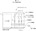
(メモリモジュールの内部構成)
図2は、メモリモジュール4Aの内部構成を示す。なお、メモリモジュール4B〜4D、5A〜5Dは、メモリモジュール4Aと同一構成であるので、以下においては説明を省略する。
(Internal configuration of memory module)
FIG. 2 shows an internal configuration of the
メモリモジュール4Aは、メモリ回路11と、メモリ回路11の信号入出力部18のライン17に接続されたバス接続部12と、メモリ回路11の信号入出力部18のライン17に一端が接続された純抵抗からなる複数の終端抵抗13と、各終端抵抗13をオンにするときにスイッチングされる複数のスイッチ14と、終端抵抗13に電源供給を行うI/O(入出力)電源端子15と、スイッチ14をオン/オフ制御するODT信号23がODT信号線21を介してメモリコントローラ2から付与されるODT制御端子16とを備えている。
図2において、メモリ回路11の信号入出力部18のライン17は、バス配線3Bに対応して、それぞれが複数本からなるデータ線、アドレス線、及びコントロール線を有している。なお、各終端抵抗13は、ライン17の各データ線に一端が接続されている。
In FIG. 2, the line 17 of the signal input / output unit 18 of the
(メモリシステムの動作)
次に、メモリシステム1の動作を図3および図4を参照して説明する。図3(a)は、メモリモジュール4Bへの書み込み動作を示し、図3(b)はメモリモジュール4Aへの書き込み動作を示し、図4(a)は、メモリモジュール4Bからの読み出し動作を示し、図4(b)はメモリモジュール4Aからの読み出し動作を示す。
(Memory system operation)
Next, the operation of the memory system 1 will be described with reference to FIGS. 3A shows a write operation to the
(1)メモリモジュール4Bへの書き込み
図3(a)において、書き込み前は、メモリモジュール4A〜5Dがスタンバイ(待機状態)にあり、それぞれの信号入出力部18は、ハイインピーダンスになっている。ここで、例えば、メモリコントローラ2からメモリモジュール4Bにデータを書き込むとすると、メモリコントローラ2は、バス配線3A,3Bを介してメモリモジュール4Bにチップセレクト信号を出力するとともに、メモリモジュール4A,5AにODT信号線21を介してODT信号23を出力する。ODT信号23は、例えば、データ入出力、データストローブ、ライトデータマスク等の信号に同期して出力される。更に、メモリコントローラ2は、メモリモジュール4A〜5Dに向けて、書き込み信号30をバス配線3Aへ出力する。
(1) Writing to
メモリコントローラ2からのチップセレクト信号を受信したメモリモジュール4Bのみがアクティブ(動作状態)になり、他のメモリモジュール4A,4C,4D,5A〜5Dは、スタンバイ状態を維持する。アクティブになったメモリモジュール4Bは、メモリコントローラ2からの書き込み信号30をメモリ回路11に書き込む動作を開始する。
Only the
一方、メモリモジュール4A,5Aでは、スタンバイ状態を維持しながら、メモリコントローラ2からのODT信号23によってスイッチ14がオンになり、これにより終端抵抗13がオン、すなわち終端抵抗13がアクティブになり、メモリモジュール4A,5Aの信号入出力部18はローインピーダンスになる。
On the other hand, in the
この結果、バス配線3B,3Cを介してメモリモジュール4A,5Aに到達した書き込み信号30は、終端抵抗13に吸収され、反射信号は信号入出力部18から発生せず、或いは抑制される。なお、終端抵抗13で吸収しきれずに信号入出力部18で反射して、メモリモジュール4A,5Aからバス配線3B,3Cへ進行した反射信号は、バス配線3B,3Cを往復する過程でメモリモジュール4A,5Aの終端抵抗13で吸収されるので、メモリモジュール4Bの書き込み信号30に影響を及ぼすことはない。
As a result, the
なお、終端抵抗13がオフのメモリモジュール4C,4D,5A〜5Cは、ハイインピーダンスにあるため、それぞれの信号入出力部18で書き込み信号30を反射する可能性があるが、反射信号が発生したとしても、その反射信号はメモリモジュール4A,5Aの終端抵抗13で吸収されるので問題は生じない。
Note that the
また、電力消費の増大は避けられないが、メモリモジュール4A,5Aと同時に、メモリモジュール4C,4D,5B〜5Dの全ての終端抵抗をオンにすることも可能であり、これによって反射信号を完全に抑制することができる。
Although increase in power consumption is inevitable, it is also possible to turn on all termination resistors of the
(2)外側のメモリモジュール4Aへの書き込み
図3(b)は、第1のメモリ群40の最も外側のメモリモジュール4Aにデータ書き込みを行うときの信号の経路を示す。この場合、メモリコントローラ2は、バス配線3A,3Bを介してメモリモジュール4Aにチップセレクト信号を出力するとともに、メモリモジュール5AにODT信号線21を介してODT信号23を出力する。更に、メモリコントローラ2は、メモリモジュール4A〜5Dに向けて、書き込み信号30をバス配線3Aへ出力する。このとき、メモリモジュール4AのODT制御端子16にはODT信号23を印加しない。これにより、メモリモジュール5Aの終端抵抗13がオンになり、メモリモジュール4Aはスイッチ14がオフになるので終端抵抗13はオープンになる。
(2) Writing to
メモリコントローラ2からのチップセレクト信号を受信したメモリモジュール4Aのみがアクティブ(動作状態)になり、他のメモリモジュール4B,4C,4D,5A〜5Dは、スタンバイ状態を維持する。アクティブになったメモリモジュール4Aは、メモリコントローラ2からの書き込み信号30をメモリ回路11に書き込む動作を開始する。
Only the
メモリコントローラ2からバス配線3Cを経てメモリモジュール5Aに向かった書き込み信号30は、メモリモジュール5Aの終端抵抗13に到達して吸収される。これにより、メモリモジュール5Aからメモリモジュール4Aに向かう反射信号は発生せず、或いは抑制され、メモリモジュール4Aの信号波形に影響を及ぼすことが無くなる。
The
なお、図3(b)において、反対側のメモリモジュール5Aにデータ書き込みを行う場合は、メモリコントローラ2によってメモリモジュール4Aの終端抵抗13をオンにし、メモリモジュール5Aの終端抵抗13をオープンにすればよい。
In FIG. 3B, when data is written to the
(3)メモリモジュール4Bからの読み出し
図4(a)は、メモリモジュール4Bからのデータ読み出し時の信号の経路を示す。例えば、メモリコントローラ2がメモリモジュール4Bからデータ信号(読み出し信号31)を読み出す場合、メモリコントローラ2は、チップセレクト信号をメモリモジュール4Bへ出力するとともに、ODT信号線21を介してメモリモジュール4A,5AのODT制御端子16にODT信号23を印加してスイッチ14をオンにし、メモリモジュール4A,5Aのそれぞれの終端抵抗13をアクティブにする。
(3) Reading from
アクティブになったメモリモジュール4Bからメモリコントローラ2によって読み出された読み出し信号31は、バス配線3B,3Aを経てメモリコントローラ2に取り込まれる。一方、メモリモジュール4Bからメモリモジュール4Aへ進行した読み出し信号31は、メモリモジュール4Aの終端抵抗13で吸収される。また、メモリモジュール4Bからバス配線3B,3Cを経てメモリモジュール5Aへ進行した読み出し信号31は、メモリモジュール5Aの終端抵抗13で吸収され、反射信号を発生せず、或いは反射信号を抑制する。
A
なお、終端抵抗13がオフのメモリモジュール4C,4D,5B〜5Dは、ハイインピーダンスにあるため、それぞれの信号入出力部18で読み出し信号31を反射する可能性があるが、反射信号が発生したとしても、その反射信号はメモリモジュール4A,5Aの終端抵抗13で吸収されるので問題は生じない。
Note that the
(4)外側のメモリモジュール4Aからの読み出し
図4(b)は、外側のメモリモジュール4Aからデータをメモリコントローラ2により読み出したときの信号の経路を示す。この場合、メモリコントローラ2は、バス配線3A,3Bを介してメモリモジュール4Aにチップセレクト信号を出力するとともに、一方の外側のメモリモジュール5AにODT信号線21を介してODT信号23を出力する。このとき、メモリモジュール4AのODT制御端子16にはODT信号23を印加しない。これにより、メモリモジュール5Aの終端抵抗13がオンになり、メモリモジュール4Aの終端抵抗13はオープンになる。
(4) Reading from
メモリモジュール4Aからメモリコントローラ2によって読み出された読み出し信号31は、バス配線3B,3Aを経てメモリコントローラ2に取り込まれる。一方、バス配線3B,3Cを経てメモリモジュール5Aに到達した読み出し信号31は、メモリモジュール5Aの終端抵抗13によって吸収され、反射信号を発生せず、或いは反射信号を抑制する。
A
メモリモジュール4Aがアクティブにあるとき、メモリモジュール4C,4D,5B〜5Dは、ハイインピーダンスにあるため、それぞれの信号入出力部18で読み出し信号31を反射する可能性があるが、反射信号が発生したとしても、その反射信号はメモリモジュール5Aの終端抵抗13で吸収されるので問題は生じない。
When the
なお、図4(b)において、反対側のメモリモジュール5Aからメモリコントローラ2によりデータを読み出す場合は、メモリコントローラ2によってメモリモジュール4Aの終端抵抗13をオンにし、メモリモジュール5Aの終端抵抗13をオープンにすればよい。
In FIG. 4B, when data is read by the
以上は、メモリモジュール4A,4B,5Aを動作させた場合であったが、その他のメモリモジュール4C,5B〜5Dのいずれかによる書き込み/読み出し時にも、両側のメモリモジュール4A,5Aの終端抵抗13をオンにすることで、メモリモジュール4A,5Aから反射信号が生じるのを抑制することができる。
The above is the case where the
(第1の実施の形態の効果)
本実施の形態によれば、下記の効果を奏する。
(イ)従来必要としたメモリコントローラ2の内部や外部に終端抵抗を設ける必要がないため、コスト低減が図れ、かつ終端抵抗による電力消費を低減することができる。
(ロ)メモリコントローラ2の近傍でバス配線をT字型にし、その両側に第1,第2のメモリ群40,50を配置し、それぞれの外側に終端抵抗13を有するメモリモジュール4A,5Aを配置した構成により、アクティブ状態にあるメモリモジュールの動作に起因する反射信号は、両側のメモリモジュール4A,5Aの終端抵抗13で吸収されるので、信号品質の向上及びメモリアクセスの高速化を図ることができる。
(ハ)バス配線3Aの長さを最短にすることにより、メモリコントローラ2の信号入出力部18における反射信号の発生を抑制することができる。
(ニ)メモリモジュール4A〜5Dからなるメモリ群の中間にメモリコントローラ2を配設したことにより、メモリコントローラ2からバス配線3A,3Bの両端のメモリモジュール4A,5Aの終端処理を自由に制御することができる。
(ホ)メモリモジュール4A,5Aは、同一バス配線に接続されている他のメモリモジュールと同等の仕様であるため、精度の良い終端処理をすることができ、それによって信号品質が向上し、メモリアクセスを高速化することができる。
(ヘ)メモリモジュール4A,5Aに接続するODT信号23用の信号線は、1つのメモリモジュールに対して2本程度であるため、配線を簡略化できるとともに配線コストを低減することができる。
(Effects of the first embodiment)
According to the present embodiment, the following effects are obtained.
(A) Since it is not necessary to provide a termination resistor inside or outside the
(B) The bus wiring is made T-shaped near the
(C) By making the length of the
(D) Since the
(E) Since the
(F) Since there are about two signal lines for the
[第2の実施の形態]
図5は、本発明の第2の実施の形態に係るメモリシステムを示す。このメモリシステム1は、第1の実施の形態において、第1のメモリ群40を終端抵抗13を備えた1つのメモリモジュール4Aで構成したものであり、他は第1の実施の形態と同様に構成されている。この構成によっても、アクティブ状態にあるメモリモジュールの動作に起因する反射信号を両側のメモリモジュール4A,5Aの終端抵抗13で吸収するので、信号品質の向上及びメモリアクセスの高速化を図ることができる。
[Second Embodiment]
FIG. 5 shows a memory system according to the second embodiment of the present invention. In the memory system 1, the
[第3の実施の形態]
図6は、本発明の第3の実施の形態に係るメモリシステムを示す。このメモリシステム1は、第1の実施の形態において、第1のメモリ群40および第2のメモリ群50をそれぞれ終端抵抗13を備えた1つのメモリモジュール4A,5Aで構成したものであり、他は第1の実施の形態と同様に構成されている。この構成によっても、アクティブ状態にあるメモリモジュールの動作に起因する反射信号をメモリモジュール4A,5Aの終端抵抗13で吸収するので、信号品質の向上及びメモリアクセスの高速化を図ることができる。
[Third Embodiment]
FIG. 6 shows a memory system according to the third embodiment of the present invention. This memory system 1 is configured by configuring the
[第4の実施の形態]
図7は、本発明の第4の実施の形態に係るメモリシステムを示す。第1の実施の形態では、バス配線を2つに分岐したが、本実施の形態は、3つに分岐したものであり、分岐されたバス配線3B,3C,3Dにそれぞれ3つのメモリモジュール4A〜4C、5A〜5C、6A〜6Cからなる第1のメモリ群40、第2のメモリ群50、第3のメモリ群60を接続したものであり、他は第1の実施の形態と同様に構成されている。この構成によっても、アクティブ状態にあるメモリモジュールの動作に起因する反射信号をメモリモジュール4A,5A,6Aの終端抵抗13で吸収するので、信号品質の向上及びメモリアクセスの高速化を図ることができる。
[Fourth Embodiment]
FIG. 7 shows a memory system according to the fourth embodiment of the present invention. In the first embodiment, the bus wiring is branched into two. However, in the present embodiment, the bus wiring is branched into three, and each of the branched
なお、第4の実施の形態において、各バス配線3B,3C,3Dのいずれか、あるいは全てのバス配線に接続するメモリモジュールは、1つでもよい。
In the fourth embodiment, one memory module may be connected to any or all of the
[他の実施の形態]
なお、本発明は、上記実施の形態に限定されず、本発明の要旨を変更しない範囲内で種々な変形が可能である。また、各実施の形態の構成要素を本発明の要旨を変更しない範囲内で任意に組合わせることが可能である。
[Other embodiments]
The present invention is not limited to the above embodiment, and various modifications can be made without departing from the scope of the present invention. In addition, the constituent elements of the respective embodiments can be arbitrarily combined within a range that does not change the gist of the present invention.
上記実施の形態では、メモリモジュールの代わりに単一の半導体メモリをバス配線に接続してもよい。 In the above embodiment, a single semiconductor memory may be connected to the bus wiring instead of the memory module.
上記実施の形態では、反射信号吸収素子は、純抵抗による終端抵抗を用いたが、誘導性及び容量性を有せず、かつ抵抗成分のみを示す素子であれば、抵抗以外の素子であってもよい。 In the above-described embodiment, the reflection signal absorbing element uses a termination resistor based on a pure resistance. However, any element other than a resistor may be used as long as it is an element that does not have inductivity and capacitance and exhibits only a resistance component. Also good.
1 メモリシステム
2 メモリコントローラ
3A,3B,3C バス配線
4A〜4D,5A〜5D メモリモジュール
11 メモリ回路
12 バス接続部
13 終端抵抗
14 スイッチ
15 I/O電源端子
16,20 ODT制御端子
17 ライン
18 信号入出力部
21 ODT信号線
23 ODT信号
30 書き込み信号
31 読み出し信号
40 第1のメモリ群
50 第2のメモリ群
DESCRIPTION OF SYMBOLS 1
Claims (5)
前記メモリコントローラから導出されて複数に分岐された複数のバス配線を有するバスと、
前記複数のバス配線にそれぞれ1つ以上のメモリを接続してなるメモリ群とを備え、
前記メモリ群に属する前記メモリのうち、前記複数のバス配線の、少なくとも前記メモリコントローラから最も離れた位置にそれぞれ接続された前記メモリは、前記反射信号吸収素子を有し、
前記メモリコントローラは、前記メモリ群の中間に配設され、前記メモリ群のうちいずれかの前記メモリがアクティブになったとき、そのアクティブになった前記メモリのバス配線以外の他のバス配線に接続された前記メモリ群に属する前記メモリのうち前記メモリコントローラから最も離れた位置に接続された前記メモリが有する前記反射信号吸収素子をオンにすることを特徴とするメモリシステム。 A memory controller having no reflected signal absorbing element ;
A bus having a plurality of bus lines derived from the memory controller and branched into a plurality of branches;
A memory group formed by connecting one or more memories to each of the plurality of bus lines,
Among the memory belonging to the memory group, said plurality of bus lines, said memory connected respectively farthest from at least the memory controller has the reflection signal absorbing element,
The memory controller is disposed in the middle of the memory group, when one of said memory of said memory group is activated, connected to the other bus lines other than the bus lines of the memory became the active A memory system comprising: turning on the reflection signal absorbing element of the memory connected to a position farthest from the memory controller among the memories belonging to the memory group .
Priority Applications (1)
| Application Number | Priority Date | Filing Date | Title |
|---|---|---|---|
| JP2006053118A JP4857815B2 (en) | 2006-02-28 | 2006-02-28 | Memory system |
Applications Claiming Priority (1)
| Application Number | Priority Date | Filing Date | Title |
|---|---|---|---|
| JP2006053118A JP4857815B2 (en) | 2006-02-28 | 2006-02-28 | Memory system |
Publications (2)
| Publication Number | Publication Date |
|---|---|
| JP2007233589A JP2007233589A (en) | 2007-09-13 |
| JP4857815B2 true JP4857815B2 (en) | 2012-01-18 |
Family
ID=38554138
Family Applications (1)
| Application Number | Title | Priority Date | Filing Date |
|---|---|---|---|
| JP2006053118A Expired - Fee Related JP4857815B2 (en) | 2006-02-28 | 2006-02-28 | Memory system |
Country Status (1)
| Country | Link |
|---|---|
| JP (1) | JP4857815B2 (en) |
Families Citing this family (3)
| Publication number | Priority date | Publication date | Assignee | Title |
|---|---|---|---|---|
| JP5019573B2 (en) | 2006-10-18 | 2012-09-05 | キヤノン株式会社 | Memory control circuit, memory system, memory control method thereof, and integrated circuit |
| JP5430880B2 (en) * | 2008-06-04 | 2014-03-05 | ピーエスフォー ルクスコ エスエイアールエル | Memory module, method of using the same, and memory system |
| JP5445072B2 (en) * | 2009-11-27 | 2014-03-19 | セイコーエプソン株式会社 | System comprising a plurality of storage devices and data transfer method therefor |
Family Cites Families (3)
| Publication number | Priority date | Publication date | Assignee | Title |
|---|---|---|---|---|
| JPH08272501A (en) * | 1995-03-31 | 1996-10-18 | Takaoka Electric Mfg Co Ltd | Termination circuit of memory module |
| JP3799251B2 (en) * | 2001-08-24 | 2006-07-19 | エルピーダメモリ株式会社 | Memory device and memory system |
| JP3821678B2 (en) * | 2001-09-06 | 2006-09-13 | エルピーダメモリ株式会社 | Memory device |
-
2006
- 2006-02-28 JP JP2006053118A patent/JP4857815B2/en not_active Expired - Fee Related
Also Published As
| Publication number | Publication date |
|---|---|
| JP2007233589A (en) | 2007-09-13 |
Similar Documents
| Publication | Publication Date | Title |
|---|---|---|
| JP4389228B2 (en) | Memory module | |
| JP3742051B2 (en) | Memory module, memory chip, and memory system | |
| KR100389928B1 (en) | Semiconductor memory system for controlling active termination | |
| US20140293671A1 (en) | Configurable Width Memory Modules | |
| JP5019573B2 (en) | Memory control circuit, memory system, memory control method thereof, and integrated circuit | |
| KR20230153531A (en) | Apparatuses and methods for configurable memory array bank architectures | |
| US9076500B2 (en) | Memory module including plural memory devices and data register buffer | |
| KR20080106328A (en) | Dynamically varying the memory agent and end impedances of the memory system and the memory agent. | |
| US9558806B1 (en) | Electronic device | |
| JP4982711B2 (en) | Memory chip structure for high-speed operation | |
| JP5599969B2 (en) | Multi-port memory and computer system including the multi-port memory | |
| US10318464B1 (en) | Memory system and method for accessing memory system | |
| JP2008234818A (en) | Semiconductor memory device | |
| JP2002109884A (en) | Memory device | |
| KR100711100B1 (en) | Memory module and memory system having same | |
| US20170110174A1 (en) | Device having multiple switching buffers for data paths controlled based on io configuration modes | |
| JP2010272168A (en) | Semiconductor device | |
| EP0847058B1 (en) | Improvements in or relating to integrated circuits | |
| US7405992B2 (en) | Method and apparatus for communicating command and address signals | |
| JP5412032B2 (en) | Semiconductor memory device | |
| JP4857815B2 (en) | Memory system | |
| JP6054017B2 (en) | Semiconductor memory device | |
| US10579280B2 (en) | On-die termination control for memory systems | |
| US7466619B2 (en) | Semiconductor memory device | |
| JP4197285B2 (en) | Memory controller |
Legal Events
| Date | Code | Title | Description |
|---|---|---|---|
| A621 | Written request for application examination |
Free format text: JAPANESE INTERMEDIATE CODE: A621 Effective date: 20081225 |
|
| A131 | Notification of reasons for refusal |
Free format text: JAPANESE INTERMEDIATE CODE: A131 Effective date: 20110712 |
|
| A521 | Written amendment |
Free format text: JAPANESE INTERMEDIATE CODE: A523 Effective date: 20110831 |
|
| RD03 | Notification of appointment of power of attorney |
Free format text: JAPANESE INTERMEDIATE CODE: A7423 Effective date: 20110831 |
|
| TRDD | Decision of grant or rejection written | ||
| A01 | Written decision to grant a patent or to grant a registration (utility model) |
Free format text: JAPANESE INTERMEDIATE CODE: A01 Effective date: 20111004 |
|
| A01 | Written decision to grant a patent or to grant a registration (utility model) |
Free format text: JAPANESE INTERMEDIATE CODE: A01 |
|
| A61 | First payment of annual fees (during grant procedure) |
Free format text: JAPANESE INTERMEDIATE CODE: A61 Effective date: 20111017 |
|
| R150 | Certificate of patent or registration of utility model |
Free format text: JAPANESE INTERMEDIATE CODE: R150 |
|
| FPAY | Renewal fee payment (event date is renewal date of database) |
Free format text: PAYMENT UNTIL: 20141111 Year of fee payment: 3 |
|
| LAPS | Cancellation because of no payment of annual fees |