JP4845598B2 - Signal detection method and noise removal method - Google Patents
Signal detection method and noise removal method Download PDFInfo
- Publication number
- JP4845598B2 JP4845598B2 JP2006155997A JP2006155997A JP4845598B2 JP 4845598 B2 JP4845598 B2 JP 4845598B2 JP 2006155997 A JP2006155997 A JP 2006155997A JP 2006155997 A JP2006155997 A JP 2006155997A JP 4845598 B2 JP4845598 B2 JP 4845598B2
- Authority
- JP
- Japan
- Prior art keywords
- signal
- point
- voltage
- noise
- waveform
- Prior art date
- Legal status (The legal status is an assumption and is not a legal conclusion. Google has not performed a legal analysis and makes no representation as to the accuracy of the status listed.)
- Expired - Fee Related
Links
Images


Landscapes
- Digital Transmission Methods That Use Modulated Carrier Waves (AREA)
Description
本発明の属する技術分野は、ディジタル信号を高周波変調し、電波としてそのディジタル信号を送信し、その電波を受信してディジタル信号を復調した時に、復調したディジタル信号が高周波変調前のディジタル信号との同一性を高める為の信号修正方法の技術分野に属する。特に、無線信号の電界強度が弱い場合や、機械が密集してノイズや同一周波数の電波が多数発射されている場合に用いられるディジタル信号の復調方法である。 The technical field to which the present invention belongs is that when a digital signal is modulated at a high frequency, the digital signal is transmitted as a radio wave, the radio signal is received and the digital signal is demodulated, the demodulated digital signal is compared with the digital signal before the high frequency modulation. It belongs to the technical field of signal correction methods for increasing the identity. In particular, this is a method for demodulating a digital signal used when the electric field strength of a radio signal is weak or when machines are crowded and many noises and radio waves of the same frequency are emitted.
ディジタル信号を高周波で変調してデータ転送を行う無線通信は、近年無線センサーネットワークの普及と共に一般化してきている。無線通信に於けるノイズ除去方法について、古くはモールス通信を行う際にフィルター特性をシャープにし、通過帯域を狭くして混信やノイズ成分を除去する方法がある。また、近年では中間周波数帯や低周波帯に於いて、A/D変換器を用いて信号波をアナログ信号からディジタル信号に置き換え、DSP(ディジタル・シグナル・プロセッサー)素子を用いて変換したディジタル信号の不要部分やノイズを除去し、更にその信号をA/D変換器を用いてアナログ信号に変換する方法が具現化されている。しかし、これらの2方法は構造が複雑であり、従って装置が大型化する為に小型装置での応用が難しく、また多くの素子を用いることから消費電流も多くなることから、コイン電池などの小電源で駆動する小型の装置には使えないとの欠点があった。 In recent years, wireless communication that performs data transfer by modulating a digital signal at a high frequency has become common with the spread of wireless sensor networks. As a method for removing noise in wireless communication, there is a method of removing interference and noise components by sharpening filter characteristics and narrowing a pass band when performing Morse communication. In recent years, in the intermediate frequency band and the low frequency band, a digital signal converted from an analog signal to a digital signal using an A / D converter and converted using a DSP (digital signal processor) element. A method of removing unnecessary portions and noise and further converting the signal into an analog signal using an A / D converter is realized. However, these two methods are complicated in structure, so that the size of the device is large, so that it is difficult to apply in a small device, and since many elements are used, the current consumption increases. There was a disadvantage that it could not be used for a small device driven by a power source.
更に、これらの2方法に於いて問題となるのは、素子特性からある特定周波数又は周波数範囲に信号波の周波数に周波数調整をしなければならない為に、水晶発振回路等で発生させた電気信号を信号波に混合して、用いる前記素子の特性に合わせた信号波の周波数を生成し、更に高調波をフィルターする機構、即ちスーパーヘテロダイン方式の機構が必要となる。従って、装置規模並びに消費電流共に増大する欠点を持つ。一方、無線装置の小型化や省電力化に伴いディスクリートの素子を用いて無線回路を組むよりもパッケージ・イン型の無線モジュール又は無線ICを用いて無線回路を組む方が調整等の点に於いても有利である。
本発明が目的とするところは、受信した信号を復調する際に受信信号の正解率を上げることであるが、本発明で用いている無線部はディジタル信号、つまりベースバンドの入力及び出力以降の無線処理、つまり信号を高周波変調してアンテナから送信し、又はアンテナで受信した高周波信号を復調してベースバンドの信号波に直す処理は全てパッケージ型の無線モジュールで行われている。即ち無線モジュール自体にハード的又はソフト的な変更を加えると無線モジュールの性能に影響を与える可能性がある為、当該無線モジュールから出力されたベースバンドの信号波に対して処理を行う必要があり、これが課題となる。 The purpose of the present invention is to increase the accuracy rate of the received signal when demodulating the received signal. However, the radio unit used in the present invention is a digital signal, that is, baseband input and output and subsequent. Wireless processing, that is, processing for high-frequency modulation of a signal and transmission from an antenna, or processing for demodulating a high-frequency signal received by the antenna and converting it to a baseband signal wave is all performed by a package-type wireless module. That is, if hardware or software changes are made to the wireless module itself, it may affect the performance of the wireless module, so it is necessary to process the baseband signal wave output from the wireless module. This is a challenge.
近年は稼働電力が著しく低いが処理速度の速い中央処理装置が登場しており、これらの中央処理装置を用いることでベースバンドの信号波形を整形することが可能となった。 In recent years, central processing devices that have a remarkably low operating power but a high processing speed have appeared, and it has become possible to shape a baseband signal waveform by using these central processing devices.
本発明の信号検知方法は、カップリング・コンデンサーを検波回路に用いる無線装置に於いて、無線で送られたディジタル信号を復調する場合に、受信波形の特徴から、本来あるべき信号位置を検出し、信号とノイズを見分ける。 The signal detection method of the present invention detects the signal position that should be originally detected from the characteristics of the received waveform when demodulating a digital signal transmitted wirelessly in a wireless device using a coupling capacitor in a detection circuit. Distinguish between signal and noise.
本発明の受信ノイズ除去方法は、カップリング・コンデンサーを検波回路に用いる無線装置に於いて、受信波形の特徴からデータの通信速度を判定する方法と前記判定方法を用いたものである。 The reception noise elimination method of the present invention uses a method for determining a data communication speed from the characteristics of a received waveform and the determination method in a radio apparatus using a coupling capacitor in a detection circuit.
本発明の号検知方法は、前記本来あるべき信号の位置と、判定された前記通信速度から、次の信号が立ち上がる時間軸上の位置を割り出し、その前後をスライスし、信号電圧を測定することで信号の立ち上がりを検知する。 The number detection method of the present invention calculates the position on the time axis where the next signal rises from the position of the signal that should be originally determined and the determined communication speed, slices before and after, and measures the signal voltage. To detect the rising edge of the signal.
また、本発明の信号検知方法は、前記信号の立ち上がりが検知されなかった場合に、信号入力がないことを判定する。 The signal detection method of the present invention determines that there is no signal input when the rising edge of the signal is not detected.
本発明で用いられた無線装置の主要部分は、ハードウエア的には前記無線モジュールを中心として構成された無線部と、その制御及び通信制御を行う中央処理装置、及び電源で構成されている。信号復調に於ける正解率を上げる為には、無線部から出力されたベースバンドの信号波を中央処理装置で希望する信号であるのか、混信信号やノイズ成分であるのかを判定する手段が用いられる。 The main part of the wireless device used in the present invention is composed of a wireless unit mainly composed of the wireless module in hardware, a central processing unit that controls and controls communication, and a power source. In order to increase the accuracy rate in signal demodulation, means to determine whether the baseband signal wave output from the radio unit is a signal desired by the central processing unit, an interference signal or a noise component is used. It is done.
また既知の方法として、通信距離に合わせたデータ転送速度、即ち通信距離を長く取る場合は通信速度を下げる方法やマンチェスター法、即ち、ディジタル信号の1(一)を送る時にディジタル信号の1とディジタル信号の0(零)を送る方法がある。無線通信に於いて、側波帯の幅を極力一定に保つ事は受信効率を上げるのに役立つが、この無線装置が環境ノイズやスパークノイズが多い環境で仕様される場合は、本来存在しない信号を除去しないと受信効率を上げることは難しい。 Further, as a known method, the data transfer speed according to the communication distance, that is, when the communication distance is long, the communication speed is reduced or the Manchester method, that is, when the digital signal 1 (one) is sent, There is a method of sending 0 (zero) of the signal. In wireless communications, keeping the sideband width as constant as possible helps to improve reception efficiency, but if this wireless device is specified in an environment with a lot of environmental noise or spark noise, it is a signal that does not exist originally. It is difficult to improve the reception efficiency without removing.
ディジタル信号による無線通信は、データの転送速度が異なる場合が多くあり、また、ある一定の速度で送ったとしても、データの送出に係わる中央処理装置で用いられる水晶発振子の周波数は個々の偏差がある為に、数値で指定された周波数と全く一致する場合は少ない。また、水晶発振子は温度に敏感な為、温度保証機能を持たない水晶振動子では、温度による周波数ドリフトがデータ転送速度に影響を与える。従って、データ通信の速度を正しく見分ける必要が先ずは出てくる。データ転送速度の見分け方として、プリアンブルを用いて計測する方法が一般的である。通常の無線通信では、プリアンブルと呼ばれる信号を送ってから、本来電送したいデータを電送する方法をとる。プリアンブルは通常1と0を交互に送る場合が多く、本発明で用いた通信でも1と0を交互に32ビット送ってからデータを送る方法をとっている。 Wireless communication using digital signals often has different data transfer speeds, and even if the data is sent at a certain speed, the frequency of the crystal oscillator used in the central processing unit related to data transmission varies from one individual to another. Therefore, there are few cases where the frequency exactly matches the frequency specified by the numerical value. In addition, since the crystal oscillator is sensitive to temperature, in a crystal resonator that does not have a temperature guarantee function, frequency drift due to temperature affects the data transfer rate. Therefore, it is first necessary to correctly identify the speed of data communication. As a method of identifying the data transfer rate, a method of measuring using a preamble is common. In normal wireless communication, a method called transmitting a signal called a preamble and then transmitting data to be originally transmitted is adopted. In many cases, 1 and 0 are sent alternately in the preamble, and even in the communication used in the present invention, data is sent after sending 1 and 0 alternately in 32 bits.
本発明は、無線装置の使用環境に於いて、環境ノイズやスパークノイズが多い場合に環境の影響を極力抑えて、本来の信号を復調する事に役立ち、よって通信の信頼性を高めることができる。また、当該無線装置を室内等干渉が多く、信号波によるアンテナ起電力が著しく下がる場合や、遠距離の通信で信号波がノイズレベルに非常に近い場合等に受信信号の正解率を上げることに役立つ。 INDUSTRIAL APPLICABILITY The present invention is useful for demodulating an original signal by minimizing the influence of the environment when there is a lot of environmental noise and spark noise in the usage environment of the wireless device, and thus can improve communication reliability. . In addition, when the radio device has a lot of interference such as indoors and the antenna electromotive force due to the signal wave is remarkably reduced, or when the signal wave is very close to the noise level in long-distance communication, the accuracy of the received signal is increased. Useful.
ディジタル通信に於けるプリアンブルは、通常1及び0の信号を交互に送るものが多い。これは受信機の検波回路を安定させる目的があり、特にカップリング・コンデンサーを検波回路に用いている場合は当該コンデンサーの電位を安定させ、信号に対しての応答を早くする効果がある。 Many preambles in digital communication usually send 1 and 0 signals alternately. This has the purpose of stabilizing the detection circuit of the receiver. In particular, when a coupling capacitor is used in the detection circuit, it has the effect of stabilizing the potential of the capacitor and speeding up the response to the signal.
カップリング・コンデンサーを用いたディジタル信号の検波回路の出力波形は、コンデンサー出力の性質をもった波形であり、この性質を生かして信号の速度を測定することが可能であり、プリアンブルが送られている間に信号波の波形から信号の長さ、つまりデータの転送速度を割り出し、これを基に本来あるべき信号をノイズと分離して行くことで、信号の判読を容易にすることができる。 The output waveform of a digital signal detection circuit using a coupling capacitor is a waveform with the characteristics of a capacitor output, and it is possible to measure the speed of the signal by utilizing this characteristic, and the preamble is sent. In the meantime, the length of the signal, that is, the data transfer rate is determined from the waveform of the signal wave, and based on this, the signal that should originally be separated from the noise can be easily read.
本発明の実験に用いられた無線装置は、OOKの信号を送受信するトランシーバモジュールにフラッシュメモリー搭載型のマイクロプロセッサーを使用した。OOK変調とは、ベースバンドの入力信号が1の時に高周波出力を出し、0の時は出力を出さない振幅変調方式の一種である。主搬送波の周波数は315MHzを用い、信号波はディジタル信号をOOK変調したものを用いた。 In the wireless device used in the experiment of the present invention, a microprocessor equipped with a flash memory is used as a transceiver module for transmitting and receiving an OOK signal. OOK modulation is a type of amplitude modulation method that outputs a high-frequency output when the baseband input signal is 1 and does not output when the input signal is 0. The frequency of the main carrier was 315 MHz, and the signal wave was a digital signal obtained by OOK modulation.
実施の方法として、プリアンブル送信時のカップリング・コンデンサーの出力電圧を用いてベースバンドのデータ転送速度を割り出す方法を実施例1に、信号波が1から0に移り、更に0から1に変化した場合の信号の立ち上がり時のピーク判定方法を実施例2に、同様に信号波が1から0に移り、更に次の信号が0だった場合のピーク判定方法を実施例3に記載する。 As an implementation method, the method of calculating the baseband data transfer rate using the output voltage of the coupling capacitor at the time of preamble transmission is changed to the first embodiment, and the signal wave is changed from 1 to 0 and further changed from 0 to 1. A peak determination method when the signal rises in this case is described in the second embodiment, and similarly, a peak determination method when the signal wave shifts from 1 to 0 and the next signal is 0 is described in the third embodiment.
本実施例では、バランスデータを用いたプリアンブルからデータ転送速度を割り出す方法について説明する。カップリング・コンデンサーを用いた検波回路に於いて、コンデンサーが示す電圧値は、信号波によってコンデンサーに蓄積された電荷が徐々に放電する為、当該検波回路からの出力波形が送信側で送ったデータの波形と異なる場合が多い。 In this embodiment, a method for determining a data transfer rate from a preamble using balance data will be described. In the detection circuit using a coupling capacitor, the voltage value indicated by the capacitor is the data that the output waveform from the detection circuit is sent on the transmission side because the charge accumulated in the capacitor is gradually discharged by the signal wave. It is often different from the waveform.
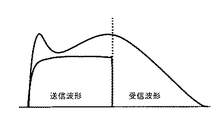
図1は、データが0から1へ、そして0に変化した時のベースバンド波形100、送信波形110及びカップリング・コンデンサーを検波回路に使用した場合の受信波形120を示す。信号が0から1に変化した時に、尖塔電圧が発生し、受信波形120に大きなピークが現れる。尖塔電圧とコンデンサーに電荷が貯まって行く課程で、一度谷間ができ、最大電圧値が見られる。ここで、送信波形110が1から0へと変化すると、電圧はコンデンサーの放電波形に従って降下していく。 FIG. 1 shows a baseband waveform 100, a transmission waveform 110, and a reception waveform 120 when a coupling capacitor is used in the detection circuit when data changes from 0 to 1 and then to 0. When the signal changes from 0 to 1, a spire voltage is generated and a large peak appears in the received waveform 120. In the process of accumulating charges in the steeple voltage and capacitor, a valley is formed once and the maximum voltage value is seen. Here, when the transmission waveform 110 changes from 1 to 0, the voltage drops according to the discharge waveform of the capacitor.
図2は送信波形と受信波形との時間的関係を表したものである。受信信号をある一定の時間毎にスライスしてその電圧を測定し、ノイズ閾値及びこの閾値を越えた信号電圧を信号電圧1とし、受信信号がノイズ閾値未満に下がった最初の信号電圧を信号電圧Nとする。その様子を図3に示す。 FIG. 2 shows a temporal relationship between the transmission waveform and the reception waveform. The received signal is sliced at certain time intervals and the voltage is measured. The noise threshold and the signal voltage exceeding the threshold are set as the signal voltage 1, and the first signal voltage when the received signal falls below the noise threshold is set as the signal voltage. N. This is shown in FIG.
次に信号電圧1から信号電圧Nの間において特異点、つまり接線の傾きが0の点が3点存在する。3点の内、信号電圧の一番低い点を図4に示す特異点Bとする。特異点Bは、他の2点の中間にあることが条件となる。特異点Bの信号電圧1側にある特異点をP1とし、土曜に特異点Bの信号電圧N側にある特異点を特異点P2とする。具体的に特異点を探す方法としては、信号電圧1から信号電圧Nまでの間で、隣り合う二つの信号電圧から傾きを測定し、傾きの符号が変わる点を特異点として取られる方法が一般的である。 Next, between the signal voltage 1 and the signal voltage N, there are three singular points, that is, points where the slope of the tangent is zero. Of the three points, the lowest point of the signal voltage is defined as a singular point B shown in FIG. The singular point B is required to be in the middle of the other two points. The singular point on the signal voltage 1 side of the singular point B is set as P1, and the singular point on the signal voltage N side of the singular point B on Saturday is set as the singular point P2. As a specific method for searching for a singular point, a method in which a slope is measured from two adjacent signal voltages between signal voltage 1 and signal voltage N, and a point where the sign of the slope changes is taken as a singular point is generally used. Is.
ノイズの閾値は数値を入力するか、信号の無い状態である一定の時間ノイズ成分を連続受信して、積算した電圧の平均値を計算したものが一般的に用いられる。 As the noise threshold value, a value obtained by inputting a numerical value or continuously receiving a noise component for a certain time in a state where there is no signal and calculating an average value of integrated voltages is generally used.
特異点P1は信号が0から1に変化した時の尖塔電圧であり、特異点P2は信号が1から0に切り替わった点である。信号波が1である状態ではコンデンサーに電荷が貯まり、電圧が上昇するが、信号波が1から0に切り替わると、コンデンサーに貯まる電荷が供給されなくなり、放電に変わるので、信号電圧が降下することになる。従って、ベースバンドの信号の長さ、時間T、は、信号電圧1から特異点P2の差にサンプリング間隔を掛け合わせたものである。図4に時間Tを示す。 The singular point P1 is the spire voltage when the signal changes from 0 to 1, and the singular point P2 is the point at which the signal switches from 1 to 0. When the signal wave is 1, the charge is stored in the capacitor and the voltage rises. However, when the signal wave is switched from 1 to 0, the charge stored in the capacitor is not supplied and changes to discharge, so the signal voltage drops. become. Therefore, the length of the baseband signal, time T, is obtained by multiplying the difference between the signal voltage 1 and the singular point P2 by the sampling interval. FIG. 4 shows time T.
本実施例では時間精度を上げる為に、32回のプリアンブルについて、最初の8回を除く24回について時間測定を行って、その結果を平均値とした。 In this example, in order to improve time accuracy, time measurement was performed for 24 times except for the first 8 times for 32 preambles, and the result was taken as an average value.
実際の受信信号をスペクトル・アナライザー等でその形状を見てみると、その形は基本的には図1〜図5に示す形状をしているものの、変形した波形も多く見受けられる。特に、尖塔電圧が特異点P2の電圧よりもかなり高い場合が多くあり、従来の様にテーブルに設定した数値を用いて0又は1の判断をした場合は、2つの異なった信号と取られる可能性があり、スパイクノイズに様にシャープな信号でなくとも、信号の誤認の恐れがあることが判った。従って、本実施例に示す方法を用いてデータ転送速度を割り出すことは、このような場合にも有効と実験的に証明された。 When the shape of an actual received signal is viewed with a spectrum analyzer or the like, the shape is basically the shape shown in FIGS. 1 to 5, but many deformed waveforms can be seen. In particular, the pinnacle voltage is often much higher than the voltage at the singular point P2, and when a value of 0 or 1 is determined using a numerical value set in a table as in the past, it can be taken as two different signals. Even if the signal is not as sharp as spike noise, it has been found that the signal may be misidentified. Therefore, it has been experimentally proved that it is effective to determine the data transfer rate by using the method shown in this embodiment.
本実施例は、実際のデータを受信する場合に於いて信号波が0から1になり、更に1から0になった後について、次の信号が1なのか0なのかを判定する場合の方法について説明する。本実施例では次の信号が1であった場合について説明する。 This embodiment is a method for determining whether the next signal is 1 or 0 after the signal wave is changed from 0 to 1 and further changed from 1 to 0 when actual data is received. Will be described. In this embodiment, a case where the next signal is 1 will be described.
前実施例で判明した特異点P2及び時間Tを用いて、信号の立ち上がりを探査する位置を決定する。信号立ち上がり探査の基点となるのが、図5の探査開始基準点である。この点は、特異点P2から時間Tだけ経過した位置にある。時間Tはベースバンドのデータ転送時間に相当する値であるから、特異点P2、つまり信号が1から0に変化した点と推測される点、から時間Tだけ経過した点の近傍で、信号波が0から1に変化する可能性がある。 Using the singular point P2 and time T found in the previous embodiment, the position for searching for the rising edge of the signal is determined. The search start reference point in FIG. 5 is the base point for signal rise search. This point is at a position after time T from the singular point P2. Since the time T is a value corresponding to the baseband data transfer time, the signal wave is near the singular point P2, that is, the point where the signal is assumed to have changed from 1 to 0, and the point after the time T has elapsed. May change from 0 to 1.
しかし、データ転送用のクロックには周波数誤差があるため、誤差分を加味した時間帯で信号の立ち上がりを探査する必要がある。 However, since there is a frequency error in the data transfer clock, it is necessary to search for the rising edge of the signal in a time zone that takes into account the error.
図6に於いて、探査開始点及び探査終了点について説明する。探査開始点は、探査基準点からある一定の時間T2だけ前に行った点にあり、ここから適当な一定間隔で信号をスライスし、その電圧を測定する。信号波のスライス及び電圧測定は、図7に示す様に探査終了点まで行う。探査終了点は、探査開始基準点より時間T2だけ遅れた位置にある。時間T2に付いては高周波の精度を決める水晶発信子の安定度に依存するので、本実施例では水晶振動子の精度をレンジで、つまり水晶振動子の精度が±10PPMだったので、主搬送波に対しレンジで20PPM前の時間軸上の位置に探査開始点を設定した。信号波が立ち上がるかの判定は、スライスした電圧値がノイズの閾値を越えることで立ち上がりが確認できるが、スパイクノイズ等の影響を考えると、少なくても2電圧測定値がノイズの閾値を越えていることが好ましい。本実施例では連続する3つのスライス測定電圧がノイズの閾値を越えることを条件とした。 In FIG. 6, the search start point and the search end point will be described. The search start point is at a point that is a certain time T2 before the search reference point. From this point, the signal is sliced at an appropriate fixed interval, and the voltage is measured. The slice of the signal wave and the voltage measurement are performed until the end of the search as shown in FIG. The search end point is at a position delayed by time T2 from the search start reference point. Since the time T2 depends on the stability of the crystal oscillator that determines the accuracy of the high frequency, in this embodiment, the accuracy of the crystal resonator is a range, that is, the accuracy of the crystal resonator is ± 10 PPM. On the other hand, the search start point is set at a position on the time axis 20PPM before the range. Whether the signal wave rises can be confirmed by the sliced voltage value exceeding the noise threshold, but considering the effects of spike noise etc., at least two voltage measurements exceed the noise threshold. Preferably it is. In this embodiment, the condition is that three consecutive slice measurement voltages exceed the noise threshold.
本発明の実施条件ではマンチェスター法を使用しており、この方法では信号波は0が2つ以上又は1が2つ以上連続することがない。従って、1が2つ連続した場合はその次に必ず0がくるはずであるので、基点となる最初の信号波の立ち上がりから時間Tを3倍した時点から図7で示す作業を行うことで、その次にくる信号が0なのか1なのか判断することができる。 In the implementation condition of the present invention, the Manchester method is used. In this method, the signal wave does not have two or more 0s or two or more consecutive 1s. Accordingly, when two 1s are consecutive, 0 is sure to come next, so by performing the operation shown in FIG. 7 from the time when the time T is tripled from the rise of the first signal wave as the base point, It can be determined whether the next signal is 0 or 1.
本実施例は、実際のデータを受信する場合に於いて信号波が0から1になり、更に1から0になった後について、次の信号が0だった場合について説明する。信号の立ち上がりを探査する方法においては、実施例2に準じる方法を用いる。 In the present embodiment, the case where the next signal is 0 after the signal wave is changed from 0 to 1 and further changed from 1 to 0 when actual data is received will be described. In the method of searching for the rising edge of the signal, a method according to the second embodiment is used.
図8を用いて信号波のピークが存在しないことを確認する方法を説明する。図7同様、信号波の立ち上がり位置と想定される場所を、時間軸に沿って探査開始点から探査終了点までスライスし、各スライス地点の信号電圧を測定する。しかし、信号が0の場合は、1の場合と異なって信号波としての入力がない為、ノイズレベルが出力される。従って、スライス電圧値が連続してノイズレベルを超えることはない。しかし、スパイクノイズの可能性も考えられる為、本来はスライス電圧値が最高となる探査開始時間から時間Tだけ時間軸を下った点、図7で言うピーク確認地点、に於いて再度、信号波をスライスし、その位置でのスライス電流値を測定する。測定したスライス電流値が、ここに於いてもスライス電流値がノイズ閾値を下回る場合には入力信号がないと判定できる。但し、ピーク確認地点でのスライス電圧値がスパークノイズ等でノイズ閾値を越え、且つ、図3のピーク閾値の70%を越えていない場合も、信号入力がないと判定する。その他の場合は、ピーク確認地点の近傍をスライスし、その値を持って判断する必要がある。近傍点をスライス値がノイズ閾値を越えていなければ、信号入力がないと判定し、ノイズ閾値を越え、且つ、図3のピーク閾値の70%を越えている場合は信号入力があると判定する。 A method for confirming that no signal wave peak exists will be described with reference to FIG. Similarly to FIG. 7, the place assumed to be the rising position of the signal wave is sliced along the time axis from the search start point to the search end point, and the signal voltage at each slice point is measured. However, when the signal is 0, unlike the case of 1, since there is no input as a signal wave, a noise level is output. Therefore, the slice voltage value does not continuously exceed the noise level. However, since there is a possibility of spike noise, the signal wave is again transmitted at the point where the time axis is lowered by the time T from the exploration start time when the slice voltage value is highest, at the peak confirmation point as shown in FIG. And slice current value at that position is measured. If the slice current value measured here is below the noise threshold value, it can be determined that there is no input signal. However, if the slice voltage value at the peak confirmation point exceeds the noise threshold due to spark noise or the like and does not exceed 70% of the peak threshold in FIG. 3, it is determined that there is no signal input. In other cases, it is necessary to slice the vicinity of the peak confirmation point and determine the value. If the slice value of the neighboring point does not exceed the noise threshold value, it is determined that there is no signal input, and if the noise threshold value is exceeded and 70% of the peak threshold value in FIG. .
本発明はノイズの多い環境下又は信号が減衰し、ノイズレベルに近づいた時にノイズと信号を識別する方法として有効である。ノイズレベルが高い場所として、工場など機械類が多い場所や電力線の近傍などが上げられる。信号が減衰した場合としては通信距離が長い場合や送信電力が低い場合などが上げられる。 The present invention is effective as a method for discriminating noise from a signal in a noisy environment or when a signal is attenuated and approaches a noise level. As a place with a high noise level, a place with a lot of machinery such as a factory, a vicinity of a power line, etc. can be raised. Examples of cases where the signal is attenuated include cases where the communication distance is long and transmission power is low.
100 ベースバンド波形
110 送信波形
120 受信波形
100 Baseband waveform 110 Transmission waveform 120 Reception waveform
Claims (3)
Priority Applications (1)
| Application Number | Priority Date | Filing Date | Title |
|---|---|---|---|
| JP2006155997A JP4845598B2 (en) | 2006-06-05 | 2006-06-05 | Signal detection method and noise removal method |
Applications Claiming Priority (1)
| Application Number | Priority Date | Filing Date | Title |
|---|---|---|---|
| JP2006155997A JP4845598B2 (en) | 2006-06-05 | 2006-06-05 | Signal detection method and noise removal method |
Publications (2)
| Publication Number | Publication Date |
|---|---|
| JP2007325184A JP2007325184A (en) | 2007-12-13 |
| JP4845598B2 true JP4845598B2 (en) | 2011-12-28 |
Family
ID=38857556
Family Applications (1)
| Application Number | Title | Priority Date | Filing Date |
|---|---|---|---|
| JP2006155997A Expired - Fee Related JP4845598B2 (en) | 2006-06-05 | 2006-06-05 | Signal detection method and noise removal method |
Country Status (1)
| Country | Link |
|---|---|
| JP (1) | JP4845598B2 (en) |
Family Cites Families (8)
| Publication number | Priority date | Publication date | Assignee | Title |
|---|---|---|---|---|
| JPH0918461A (en) * | 1995-06-26 | 1997-01-17 | Atsumi Electron Corp Ltd | Data receiver |
| JP4006889B2 (en) * | 1999-06-14 | 2007-11-14 | 株式会社デンソー | Receiver |
| JP2001292183A (en) * | 2000-04-06 | 2001-10-19 | Nippon Telegr & Teleph Corp <Ntt> | Ask-demodulation circuit |
| EP1413104A1 (en) * | 2001-07-20 | 2004-04-28 | Koninklijke Philips Electronics N.V. | Data rate acquisition using signal edges |
| JP2003125012A (en) * | 2001-10-16 | 2003-04-25 | Matsushita Electric Ind Co Ltd | Ask demodulator with agc |
| JP2003198645A (en) * | 2001-12-27 | 2003-07-11 | Sharp Corp | Transmitter and communication system using the same |
| JP3908643B2 (en) * | 2002-10-18 | 2007-04-25 | 東芝マイクロエレクトロニクス株式会社 | Digital signal demodulation circuit |
| JP2004362617A (en) * | 2004-09-10 | 2004-12-24 | Matsushita Electric Ind Co Ltd | Ic card connection device and its connection method |
-
2006
- 2006-06-05 JP JP2006155997A patent/JP4845598B2/en not_active Expired - Fee Related
Also Published As
| Publication number | Publication date |
|---|---|
| JP2007325184A (en) | 2007-12-13 |
Similar Documents
| Publication | Publication Date | Title |
|---|---|---|
| CN102047576B (en) | Reception device | |
| US8204099B2 (en) | Signal processing unit and wireless communication device | |
| CN1883121B (en) | Method and apparatus for accurately detecting validity of a received signal | |
| EP2241013B1 (en) | Power supply control in a wireless receiver | |
| JP4845598B2 (en) | Signal detection method and noise removal method | |
| JP4755077B2 (en) | Transmission mode, guard length detection circuit and method | |
| US9094265B1 (en) | Receiving apparatus and demodulation method | |
| US8909145B2 (en) | Wireless telemetry auto for torque measurement system | |
| US10142143B2 (en) | Receiving apparatus and demodulation method | |
| EP2124349A1 (en) | Wireless communication device | |
| EP2839245B1 (en) | Method and system for energy efficient measurement of sensor signals | |
| GB2532491A (en) | AM demodulation | |
| US9225567B2 (en) | Receiving apparatus and demodulation method | |
| JP2007013406A (en) | Fsk receiving device | |
| JP2007292613A (en) | Circuit for receiving standard electric wave | |
| US9191189B2 (en) | Method and apparatus for detecting a preamble in a received radio signal | |
| US8233519B2 (en) | Signal processing unit and wireless communication device | |
| CN110235379B (en) | Method for performing clear channel assessment and radio receiver | |
| EP3393050B1 (en) | Wireless receiver | |
| US9595984B2 (en) | Concept for transmitting and receiving an information symbol | |
| CN116112042B (en) | Demodulation circuit, electronic tag and electronic tag system | |
| JP2019021963A (en) | Demodulator and demodulation method | |
| CN112688892B (en) | Subcarrier detection method, carrier signal demodulation method and demodulation device | |
| KR101037431B1 (en) | Analog front-end filter for dual mode modulation and demodulation of ook and fsk modulated signals | |
| JP5840378B2 (en) | Wireless transmission device and wireless reception device |
Legal Events
| Date | Code | Title | Description |
|---|---|---|---|
| A621 | Written request for application examination |
Free format text: JAPANESE INTERMEDIATE CODE: A621 Effective date: 20090220 |
|
| RD01 | Notification of change of attorney |
Free format text: JAPANESE INTERMEDIATE CODE: A7421 Effective date: 20091105 |
|
| RD01 | Notification of change of attorney |
Free format text: JAPANESE INTERMEDIATE CODE: A7421 Effective date: 20091113 |
|
| RD01 | Notification of change of attorney |
Free format text: JAPANESE INTERMEDIATE CODE: A7421 Effective date: 20091118 |
|
| A977 | Report on retrieval |
Free format text: JAPANESE INTERMEDIATE CODE: A971007 Effective date: 20110304 |
|
| A131 | Notification of reasons for refusal |
Free format text: JAPANESE INTERMEDIATE CODE: A131 Effective date: 20110712 |
|
| A521 | Written amendment |
Free format text: JAPANESE INTERMEDIATE CODE: A523 Effective date: 20110905 |
|
| TRDD | Decision of grant or rejection written | ||
| A01 | Written decision to grant a patent or to grant a registration (utility model) |
Free format text: JAPANESE INTERMEDIATE CODE: A01 Effective date: 20111004 |
|
| A01 | Written decision to grant a patent or to grant a registration (utility model) |
Free format text: JAPANESE INTERMEDIATE CODE: A01 |
|
| A61 | First payment of annual fees (during grant procedure) |
Free format text: JAPANESE INTERMEDIATE CODE: A61 Effective date: 20111011 |
|
| FPAY | Renewal fee payment (event date is renewal date of database) |
Free format text: PAYMENT UNTIL: 20141021 Year of fee payment: 3 |
|
| R150 | Certificate of patent or registration of utility model |
Free format text: JAPANESE INTERMEDIATE CODE: R150 |
|
| R250 | Receipt of annual fees |
Free format text: JAPANESE INTERMEDIATE CODE: R250 |
|
| LAPS | Cancellation because of no payment of annual fees |