JP4842942B2 - Wireless receiver - Google Patents
Wireless receiver Download PDFInfo
- Publication number
- JP4842942B2 JP4842942B2 JP2007522258A JP2007522258A JP4842942B2 JP 4842942 B2 JP4842942 B2 JP 4842942B2 JP 2007522258 A JP2007522258 A JP 2007522258A JP 2007522258 A JP2007522258 A JP 2007522258A JP 4842942 B2 JP4842942 B2 JP 4842942B2
- Authority
- JP
- Japan
- Prior art keywords
- frequency
- signal
- unit
- digital
- band
- Prior art date
- Legal status (The legal status is an assumption and is not a legal conclusion. Google has not performed a legal analysis and makes no representation as to the accuracy of the status listed.)
- Expired - Fee Related
Links
Images


Classifications
-
- H—ELECTRICITY
- H04—ELECTRIC COMMUNICATION TECHNIQUE
- H04B—TRANSMISSION
- H04B1/00—Details of transmission systems, not covered by a single one of groups H04B3/00 - H04B13/00; Details of transmission systems not characterised by the medium used for transmission
- H04B1/005—Details of transmission systems, not covered by a single one of groups H04B3/00 - H04B13/00; Details of transmission systems not characterised by the medium used for transmission adapting radio receivers, transmitters andtransceivers for operation on two or more bands, i.e. frequency ranges
-
- H—ELECTRICITY
- H03—ELECTRONIC CIRCUITRY
- H03D—DEMODULATION OR TRANSFERENCE OF MODULATION FROM ONE CARRIER TO ANOTHER
- H03D3/00—Demodulation of angle-, frequency- or phase- modulated oscillations
- H03D3/007—Demodulation of angle-, frequency- or phase- modulated oscillations by converting the oscillations into two quadrature related signals
-
- H—ELECTRICITY
- H03—ELECTRONIC CIRCUITRY
- H03J—TUNING RESONANT CIRCUITS; SELECTING RESONANT CIRCUITS
- H03J1/00—Details of adjusting, driving, indicating, or mechanical control arrangements for resonant circuits in general
- H03J1/0008—Details of adjusting, driving, indicating, or mechanical control arrangements for resonant circuits in general using a central processing unit, e.g. a microprocessor
- H03J1/0041—Details of adjusting, driving, indicating, or mechanical control arrangements for resonant circuits in general using a central processing unit, e.g. a microprocessor for frequency synthesis with counters or frequency dividers
- H03J1/005—Details of adjusting, driving, indicating, or mechanical control arrangements for resonant circuits in general using a central processing unit, e.g. a microprocessor for frequency synthesis with counters or frequency dividers in a loop
-
- H—ELECTRICITY
- H03—ELECTRONIC CIRCUITRY
- H03L—AUTOMATIC CONTROL, STARTING, SYNCHRONISATION OR STABILISATION OF GENERATORS OF ELECTRONIC OSCILLATIONS OR PULSES
- H03L7/00—Automatic control of frequency or phase; Synchronisation
- H03L7/06—Automatic control of frequency or phase; Synchronisation using a reference signal applied to a frequency- or phase-locked loop
- H03L7/08—Details of the phase-locked loop
- H03L7/099—Details of the phase-locked loop concerning mainly the controlled oscillator of the loop
-
- H—ELECTRICITY
- H03—ELECTRONIC CIRCUITRY
- H03L—AUTOMATIC CONTROL, STARTING, SYNCHRONISATION OR STABILISATION OF GENERATORS OF ELECTRONIC OSCILLATIONS OR PULSES
- H03L7/00—Automatic control of frequency or phase; Synchronisation
- H03L7/06—Automatic control of frequency or phase; Synchronisation using a reference signal applied to a frequency- or phase-locked loop
- H03L7/08—Details of the phase-locked loop
- H03L7/10—Details of the phase-locked loop for assuring initial synchronisation or for broadening the capture range
-
- H—ELECTRICITY
- H03—ELECTRONIC CIRCUITRY
- H03L—AUTOMATIC CONTROL, STARTING, SYNCHRONISATION OR STABILISATION OF GENERATORS OF ELECTRONIC OSCILLATIONS OR PULSES
- H03L7/00—Automatic control of frequency or phase; Synchronisation
- H03L7/06—Automatic control of frequency or phase; Synchronisation using a reference signal applied to a frequency- or phase-locked loop
- H03L7/16—Indirect frequency synthesis, i.e. generating a desired one of a number of predetermined frequencies using a frequency- or phase-locked loop
- H03L7/18—Indirect frequency synthesis, i.e. generating a desired one of a number of predetermined frequencies using a frequency- or phase-locked loop using a frequency divider or counter in the loop
-
- H—ELECTRICITY
- H03—ELECTRONIC CIRCUITRY
- H03J—TUNING RESONANT CIRCUITS; SELECTING RESONANT CIRCUITS
- H03J2200/00—Indexing scheme relating to tuning resonant circuits and selecting resonant circuits
- H03J2200/10—Tuning of a resonator by means of digitally controlled capacitor bank
Landscapes
- Engineering & Computer Science (AREA)
- Computer Hardware Design (AREA)
- Microelectronics & Electronic Packaging (AREA)
- Computer Networks & Wireless Communication (AREA)
- Signal Processing (AREA)
- Power Engineering (AREA)
- Superheterodyne Receivers (AREA)
Description
本発明は、移動体端末に用いられる無線受信装置に関し、より特定的には、マルチバンド、またはマルチモードの無線受信装置に関する。 The present invention relates to a radio reception apparatus used for a mobile terminal, and more particularly to a multiband or multimode radio reception apparatus.
近年、移動体通信は全世界レベルで発展している。地域、データ量、人口密度などに関わらず、1つの端末によって通信を実現するために、当該端末内の無線回路には、異なる通信方式をサポートできるマルチモード(マルチレート、またはマルチキャリアともいう)および/または異なる周波数帯をサポートできるマルチバンドの機能が要求されている。 In recent years, mobile communication has been developed at the world level. Multi-mode (also referred to as multi-rate or multi-carrier) capable of supporting different communication methods in a wireless circuit in the terminal in order to realize communication by one terminal regardless of region, data amount, population density, etc. There is a need for multiband capabilities that can support different frequency bands.
当然、モード毎、またはバンド毎に、複数の無線回路を用意すれば、このような機能は実現できる。しかし、複数の無線回路を1つの端末に内蔵することは、部品点数の増加、電流を供給するための配線の増加につながり、端末の大きさが携帯するには大きくなりすぎる。同時に、コストが高くなる。そのため、1つの無線回路でこのような機能を実現することが必須となる。 Naturally, such a function can be realized if a plurality of wireless circuits are prepared for each mode or for each band. However, incorporating a plurality of wireless circuits in one terminal leads to an increase in the number of parts and an increase in wiring for supplying current, and the size of the terminal becomes too large to carry. At the same time, the cost is high. Therefore, it is essential to realize such a function with one wireless circuit.
特許文献1には、従来のマルチバンド受信回路が開示されている。特許文献1のマルチバンド受信回路は、バンド選択用の局部発振器とチャネル選択用の局部発振器とを備える。当該マルチバンド受信回路は、両発振器の出力をミキシングした信号を、RFミキサのローカル信号として用いる。特許文献1のような構成をとることによって、バンド選択用の局部発振器は、ループ帯域を広く取ることが可能となる。そのため、C/Nが改善し、その分低消費電力化が可能となる。また、発振周波数が低いため、チャネル選択用局部発振器の消費電力は、RFチャネル選択用発振器と比べると小さい。結果、特許文献1の従来のマルチバンド受信回路は、1つのRFチャネル選択用発振器を用いるよりも、トータルとして低消費電力化を実現することができる。
特許文献2には、従来のマルチバンド/マルチレート受信回路が開示されている。特許文献2の従来のマルチバンド/マルチレート受信回路では、複数チャネルの受信信号が全て1つのIFフィルタを通過するように、第1局部発振器が選ばれている。そして、複数の直交復調器を用いて、復調結果を選択することによって、マルチレート化を実現している。また、特許文献2では、バンドの異なる複数の受信信号によるマルチレート化に対しては、第1局部発振器を複数個用意することによって、受信信号がすべてIFフィルタの通過帯域となるようにしている。
特許文献3には、従来のマルチキャリア受信回路が開示されている。特許文献3の従来のマルチキャリア受信回路では、複数チャネルの受信信号は、RFミキサでIF周波数にダウンコンバートされた後、複数個の経路に分けられる。各経路には、異なる周波数のフィルタが設けられ、当該フィルタが、各チャネルの信号のみを通過する。フィルタを通過した信号が復調される。このような構成にすることによって、1つのRFの経路でマルチキャリアの受信回路が実現できる。
しかし、特許文献1に記載の従来のマルチバンド受信回路には、アナログの発振器が2つ必要であるという問題が存在する。さらに2つの発振器の出力信号を混合するアナログのミキサが必要となる。アナログ回路は、補正の必要性などを考えると低消費電力化には限界がある。さらに、近年のマルチモード、またはマルチバンドのシステムでは、バンドが大きく変化するので、特許文献1に記載の従来のマルチバンド受信回路では、対応が困難である。
However, the conventional multiband receiving circuit described in
特許文献2に記載の従来のマルチバンド/マルチレート受信回路は、同一バンド内のある受信チャネルから他の受信チャネルへ切り換えるときに、第1局部発振器の周波数を変化させる必要がある。そのため、第1局部発振器の周波数をチャネル間隔のステップで変化させる必要ある。そのような細かいステップの切換のためには、多くの消費電力が必要となる。また、異なるバンド用に複数個の発振器を用いているため、小型化が困難となる。
The conventional multiband / multirate receiving circuit described in
特許文献3に記載の従来のマルチキャリア受信回路では、複数のIFの回路が必要となる。そのため、受信回路が大きくなる。また、受信バンド内に、IFの回路が対応可能なチャネル以外のチャネルが存在する場合、そもそも、特許文献3に記載の従来のマルチキャリア受信回路では、対応が不可能であるので、マルチバンドのシステムには、対応が困難である。
In the conventional multicarrier receiving circuit described in
一般に、RFアナログの局部発振器には、製造バラツキが存在する。したがって、RFアナログの局部発振器を用いて、マルチモードまたはマルチバンドに対応するためには、製造バラツキを補償しておく必要がある。製造バラツキを補償して、各モードまたは各バンドに適切な局部発振信号を得るためには、局部発振信号の帯域幅にゆとり(マージン)を持たせておく必要がある。そのため、従来構成では、局部発振周波数を適切な値にロックするために、このようなマージンの分だけ発振周波数範囲の広い局部発振器が必要となる。したがって、多くの消費電力が必要となっていた。 Generally, there are manufacturing variations in RF analog local oscillators. Therefore, it is necessary to compensate for manufacturing variations in order to support multimode or multiband using an RF analog local oscillator. In order to compensate for manufacturing variations and obtain a local oscillation signal suitable for each mode or each band, it is necessary to allow a margin (margin) in the bandwidth of the local oscillation signal. Therefore, in the conventional configuration, in order to lock the local oscillation frequency to an appropriate value, a local oscillator having a wide oscillation frequency range corresponding to such a margin is required. Therefore, much power consumption has been required.
それゆえ、本発明の目的は、RFアナログの局部発振器の消費電力を低減しながらも、マルチバンドおよびマルチモードを実現することができる無線受信装置を提供することである。 SUMMARY OF THE INVENTION Therefore, an object of the present invention is to provide a wireless receiver capable of realizing multiband and multimode while reducing power consumption of an RF analog local oscillator.
上記課題を解決するために、本発明は、以下のような特徴を有する。本発明は、受信した無線周波数信号を、中間周波数信号に変換して復調する無線受信装置であって、受信すべき無線周波数信号の周波数帯に対応する局部発振信号のバンドを、周波数帯に応じて不連続に切り換えて、局部発振信号を出力する局部発振器と、局部発振器から出力される局部発振信号によって、無線周波数信号を中間周波数信号に変換して出力する周波数変換器と、周波数変換器から出力される中間周波数信号を復調する復調器とを備える。局部発振器は、周波数帯における局部発振信号の周波数変化幅を検出し、周波数変化幅の周波数の中から、シンボルレートの整数倍となる周波数を求め、中間周波数信号における受信すべきチャネルの中心周波数をシンボルレートの整数倍の周波数にさせるための局部発振周波数を有する局部発振信号を出力する。 In order to solve the above problems, the present invention has the following features. The present invention is a radio receiving apparatus that converts a received radio frequency signal into an intermediate frequency signal and demodulates it, and determines a local oscillation signal band corresponding to the frequency band of the radio frequency signal to be received according to the frequency band. A local oscillator that outputs a local oscillation signal, a frequency converter that converts a radio frequency signal into an intermediate frequency signal by a local oscillation signal that is output from the local oscillator, and a frequency converter And a demodulator that demodulates the output intermediate frequency signal. The local oscillator detects the frequency change width of the local oscillation signal in the frequency band, obtains a frequency that is an integral multiple of the symbol rate from the frequency change width, and determines the center frequency of the channel to be received in the intermediate frequency signal. A local oscillation signal having a local oscillation frequency for making the frequency an integer multiple of the symbol rate is output.
本発明によれば、局部発振器は、中間周波数をシンボルレートの整数倍にするような周波数を有する局部発振信号を出力することとなる。中間周波数をシンボルレートの整数倍とすることによって、復調器は、アナログデジタル変換を容易に実行することができ、かつ、所望のチャネルを容易に選択することができる。復調器において所望のチャネルが選択されるので、復調器の前段においては、バンドを選択するだけでよい。中間周波数をシンボルレートの整数倍にすることができる局部発振周波数は複数存在する。したがって、局部発振器にバラツキがあったとしても、そのような局部発振周波数を選択することは可能である。よって、局部発振器は、バンドに対応して、不連続にバンドを切り替えることができ、かつ、制御電圧に対して、緩やかに局部発振周波数が変化する特性を有してさえいればよい。そのような電圧制御発振器116は、消費電力が従来に比べて少なくてよい。したがって、RFアナログの局部発振器の消費電力を低減しながらも、マルチバンドおよびマルチモードを実現することができる無線受信装置が提供されることとなる。
According to the present invention, the local oscillator outputs a local oscillation signal having a frequency that makes the intermediate frequency an integer multiple of the symbol rate. By setting the intermediate frequency to an integral multiple of the symbol rate, the demodulator can easily perform analog-to-digital conversion and can easily select a desired channel. Since a desired channel is selected in the demodulator, it is only necessary to select a band in the preceding stage of the demodulator. There are a plurality of local oscillation frequencies that can make the intermediate frequency an integer multiple of the symbol rate. Therefore, even if there are variations in the local oscillator, it is possible to select such a local oscillation frequency. Therefore, the local oscillator only needs to have a characteristic that the band can be switched discontinuously corresponding to the band and the local oscillation frequency changes gently with respect to the control voltage. Such a voltage-controlled
好ましくは、局部発振器は、バンド切り換え機能を有する電圧制御発振器から出力される信号を局部発振信号として固定するためのPLL(Phase Locked Loop)回路と、局部発振信号のバンドが切り換えられたら、電圧制御発振器から出力される信号をスイープさせる周波数制御部と、周波数制御部によるスイープの結果に基づいて、周波数変化幅を検出する検出部と、検出部によって検出された周波数変化幅の中から、シンボルレートの整数倍となる周波数を判定する判定部とを含む。周波数制御部は、判定部によって判定されたシンボルレートの整数倍の周波数に基づいて、PLL回路から出力される局部発振信号の局部発振周波数を制御する。 Preferably, the local oscillator includes a PLL (Phase Locked Loop) circuit for fixing a signal output from the voltage controlled oscillator having a band switching function as a local oscillation signal, and voltage control when the band of the local oscillation signal is switched. A frequency control unit that sweeps a signal output from the oscillator, a detection unit that detects a frequency change width based on a result of the sweep by the frequency control unit, and a symbol rate from among the frequency change widths detected by the detection unit And a determination unit that determines a frequency that is an integer multiple of. The frequency control unit controls the local oscillation frequency of the local oscillation signal output from the PLL circuit based on a frequency that is an integer multiple of the symbol rate determined by the determination unit.
これにより、電圧制御発振器の特性がばらついていたとしても、周波数変化幅を求めることができ、当該周波数変化幅の中から、適切な局部発振周波数を求めることができる。 Thereby, even if the characteristics of the voltage controlled oscillator vary, the frequency change width can be obtained, and an appropriate local oscillation frequency can be obtained from the frequency change width.
一実施形態として、周波数制御部は、PLL回路に含まれる可変分周器の分周数を制御することによって、局部発振周波数を制御し、検出部は、PLL回路に含まれるチャージポンプの電圧に基づいて、周波数変化幅を検出する。 As one embodiment, the frequency control unit controls the local oscillation frequency by controlling the frequency division number of the variable frequency divider included in the PLL circuit, and the detection unit controls the voltage of the charge pump included in the PLL circuit. Based on this, the frequency change width is detected.
これにより、基本的な回路構成によって、適切な局部発振周波数を求めることができる。 Thereby, an appropriate local oscillation frequency can be obtained by a basic circuit configuration.
一実施形態として、電圧制御発振器は、キャパシタの接続数を切り換えることによって、局部発振信号のバンドを切り換えるためのスイッチ回路と、局部発振信号の周波数を周波数変化幅の範囲で変化させるためのバラクタダイオード有する可変容量回路とを含む。 As one embodiment, a voltage-controlled oscillator includes a switch circuit for switching a band of a local oscillation signal by switching the number of capacitors connected, and a varactor diode for changing the frequency of the local oscillation signal within a range of frequency change width Having a variable capacitance circuit.
このように、本発明には、一般的な電圧制御発振器を用いることができ、電圧制御発振器に特別な精度は要求されない。よって、量産性に優れ、安価な無線受信装置を提供することができる。 Thus, a general voltage controlled oscillator can be used in the present invention, and no special accuracy is required for the voltage controlled oscillator. Therefore, it is possible to provide an inexpensive wireless reception device that is excellent in mass productivity.
一実施形態として、電圧制御発振器は、キャパシタの接続数を切り換えることによって、局部発振信号のバンドを切り換えるための第1のスイッチ回路と、キャパシタの接続数を切り換えることによって、局部発振信号の周波数を周波数変化幅の範囲で変化させるための第2のスイッチ回路とを有する。 As one embodiment, the voltage controlled oscillator includes a first switch circuit for switching a band of the local oscillation signal by switching the number of connections of the capacitor, and a frequency of the local oscillation signal by switching the number of connections of the capacitor. And a second switch circuit for changing the frequency change range.
これにより、第2のスイッチ回路の高速切り換えによって、2つの容量の中間の値を等価的に実現できる。このように、本発明には、一般的な電圧制御発振器を用いることができ、電圧制御発振器に特別な精度は要求されない。よって、量産性に優れ、安価な無線受信装置を提供することができる。 Thereby, an intermediate value between the two capacitors can be equivalently realized by high-speed switching of the second switch circuit. Thus, a general voltage controlled oscillator can be used in the present invention, and no special accuracy is required for the voltage controlled oscillator. Therefore, it is possible to provide an inexpensive wireless reception device that is excellent in mass productivity.
好ましくは、局部発振器は、中心周波数をシンボルレートの整数倍とさせる局部発振周波数が複数ある場合、複数の局部発振周波数の内、当該可変周波数範囲の真ん中の局部発振周波数を選択するとよい。 Preferably, when there are a plurality of local oscillation frequencies that cause the center frequency to be an integral multiple of the symbol rate, the local oscillator may select the local oscillation frequency in the middle of the variable frequency range among the plurality of local oscillation frequencies.
これにより、温度変化や電圧変化でIF周波数を変更する可能性が小さい無線受信装置が実現できる。 As a result, it is possible to realize a wireless reception device that is less likely to change the IF frequency due to temperature changes or voltage changes.
好ましくは、復調器は、受信したいバンドに対応する中間周波数信号を全て通過させる帯域通過フィルタと、シンボルレートの整数倍のサンプリング周波数を有するサンプリング用クロック信号に基づいて、帯域通過フィルタを通過した中間周波数信号をデジタル信号に変換するアナログデジタル変換部と、アナログデジタル変換部によって得られたデジタル信号から所望のチャネルを選択するチャネル選択部とを含む。 Preferably, the demodulator uses a band-pass filter that passes all intermediate frequency signals corresponding to a band to be received and a sampling clock signal that has a sampling frequency that is an integer multiple of the symbol rate, and that has passed through the band-pass filter. An analog-to-digital converter that converts the frequency signal into a digital signal and a channel selector that selects a desired channel from the digital signal obtained by the analog-to-digital converter.
中間周波数信号の中心周波数は、シンボルレートの整数倍としているので、このような構成の復調器を用いることによって、容易にデジタル信号を得ることができ、かつ容易に所望のチャネルを選択することができる。 Since the center frequency of the intermediate frequency signal is an integer multiple of the symbol rate, a digital signal can be easily obtained and a desired channel can be easily selected by using the demodulator having such a configuration. it can.
一実施形態として、チャネル選択部は、アナログデジタル変換部から出力されるデジタル信号の内、所望のチャネルをベースバンドにダウンコンバートするためのチャネル選択用クロック信号を生成するクロック生成部と、クロック生成部によって生成されたチャネル選択用クロック信号とアナログデジタル変換部によって得られたデジタル信号とをミキシングして、所望のチャンネルをベースバンド帯域にダウンコンバートするミキシング部と、ミキシング部によるミキシング後のデジタル信号から、所望のチャンネルのみを通過させるチャネル選択用フィルタ部とを含む。 As one embodiment, the channel selection unit includes a clock generation unit that generates a channel selection clock signal for down-converting a desired channel to a baseband among digital signals output from the analog-digital conversion unit, and a clock generation unit A mixing unit that mixes the channel selection clock signal generated by the unit and the digital signal obtained by the analog-to-digital conversion unit to down-convert a desired channel to the baseband, and a digital signal after mixing by the mixing unit To a channel selection filter section that allows only a desired channel to pass therethrough.
中間周波数信号の中心周波数は、シンボルレートの整数倍としているので、このような構成の復調器を用いることによって、容易にデジタル信号を得ることができ、かつ容易に所望のチャネルを選択することができる。 Since the center frequency of the intermediate frequency signal is an integer multiple of the symbol rate, a digital signal can be easily obtained and a desired channel can be easily selected by using the demodulator having such a configuration. it can.
一実施形態として、チャネル選択部は、サンプリング用クロック信号に基づいて、アナログデジタル変換部によって得られたデジタル信号から、所望のチャネルを選択するチャネル選択用フィルタ部と、チャネル選択用フィルタ部によって選択された所望のチャネルのデジタル信号をベースバンド帯域にダウンコンバートするためのチャネル選択用クロック信号を生成するクロック生成部と、クロック生成部によって生成されたチャネル選択用クロック信号とアナログデジタル変換部によって得られたデジタル信号とをミキシングして、所望のチャンネルをベースバンドにダウンコンバートするミキシング部とを含む。 As one embodiment, the channel selection unit is selected by the channel selection filter unit that selects a desired channel from the digital signal obtained by the analog-digital conversion unit based on the sampling clock signal, and the channel selection filter unit A clock generation unit that generates a channel selection clock signal for down-converting the digital signal of the desired channel to a baseband band, a channel selection clock signal generated by the clock generation unit, and an analog-to-digital conversion unit. And a mixing unit that mixes the received digital signal and down-converts a desired channel into a baseband.
中間周波数信号の中心周波数は、シンボルレートの整数倍としているので、このような構成の復調器を用いることによって、容易にデジタル信号を得ることができ、かつ容易に所望のチャネルを選択することができる。 Since the center frequency of the intermediate frequency signal is an integer multiple of the symbol rate, a digital signal can be easily obtained and a desired channel can be easily selected by using the demodulator having such a configuration. it can.
一実施形態として、チャネル選択部は、アナログデジタル変換部によって得られたデジタル信号をデジタルフーリエ変換するためのデジタルフーリエ変換部と、デジタルフーリエ変換部によって得られた周波数成分を少なくとも1つ選択する周波数成分選択部と、周波数選択部によって選択された少なくとも1つの周波数成分をベースバンド帯域にシフトする周波数シフト部と、周波数シフト部によって周波数シフトされた少なくとも1つの周波数成分を逆デジタルフーリエ変換することによって、所望のチャネルを選択する逆デジタルフーリエ変換部とを含む。 As an embodiment, the channel selection unit selects at least one frequency component obtained by the digital Fourier transform unit for digital Fourier transforming the digital signal obtained by the analog-digital conversion unit and the digital Fourier transform unit. A component selection unit, a frequency shift unit that shifts at least one frequency component selected by the frequency selection unit to a baseband, and an inverse digital Fourier transform on at least one frequency component frequency-shifted by the frequency shift unit And an inverse digital Fourier transform unit for selecting a desired channel.
中間周波数信号の中心周波数は、シンボルレートの整数倍としているので、このような構成の復調器を用いることによって、容易にデジタル信号を得ることができ、かつ容易に所望のチャネルを選択することができる。 Since the center frequency of the intermediate frequency signal is an integer multiple of the symbol rate, a digital signal can be easily obtained and a desired channel can be easily selected by using the demodulator having such a configuration. it can.
一実施形態として、サンプリング周波数は、中間周波数信号における受信すべきチャネルの中心周波数の2倍未満であり、アナログデジタル変換部は、帯域通過フィルタを通過した中間周波数信号の全てを、サンプリング周波数の2分の1の周波数を有するデジタル信号に変換する。 In one embodiment, the sampling frequency is less than twice the center frequency of the channel to be received in the intermediate frequency signal, and the analog-to-digital converter converts all of the intermediate frequency signal that has passed through the bandpass filter to 2 of the sampling frequency. Convert to a digital signal with a fraction of the frequency.
これにより、アナログデジタル変換部から出力されたデジタル信号をサンプリング周波数の2分の1の周波数にまでダウンコンバートすることができるので、デジタル信号をベースバンド帯域にまでダウンコンバートするためのクロック周波数を下げることができる。よって、低消費電力化が図られる。 As a result, the digital signal output from the analog-to-digital converter can be down-converted to half the sampling frequency, so the clock frequency for down-converting the digital signal to the baseband is lowered. be able to. Therefore, power consumption can be reduced.
一実施形態として、サンプリング周波数は、中間周波数における受信すべきチャネルの中間周波数の2倍未満であり、中間周波数信号は、サンプリング周波数の2分の1のN倍(Nは1以上の整数)以上、サンプリング周波数の2分の1の(N+1)倍以下の周波数を有する。 In one embodiment, the sampling frequency is less than twice the intermediate frequency of the channel to be received at the intermediate frequency, and the intermediate frequency signal is N times half the sampling frequency (N is an integer greater than or equal to 1). , Having a frequency equal to or lower than (N + 1) times half of the sampling frequency.
これにより、アナログデジタル変換部から出力されたデジタル信号をサンプリング周波数の2分の1の周波数にまでダウンコンバートすることができるので、デジタル信号をベースバンド帯域にまでダウンコンバートするためのクロック周波数を下げることができる。よって、低消費電力化が図られる。 As a result, the digital signal output from the analog-to-digital converter can be down-converted to half the sampling frequency, so the clock frequency for down-converting the digital signal to the baseband is lowered. be able to. Therefore, power consumption can be reduced.
好ましくは、復調器は、通過帯域幅が1チャネルの帯域幅よりも大きくかつ無線周波数信号の1バンド当たりの帯域幅よりも小さく、通過帯域の中心周波数が可変な中心周波数可変帯域通過フィルタと、シンボルレートの整数倍のサンプリング周波数を有するサンプリング用クロック信号に基づいて、中心周波数可変帯域通過フィルタを通過した中間周波数信号をデジタル信号に変換するアナログデジタル変換部と、アナログデジタル変換部によって得られたデジタル信号から所望のチャネルを選択するチャネル選択部とを含む。 Preferably, the demodulator has a center frequency variable bandpass filter whose passband width is larger than the bandwidth of one channel and smaller than the bandwidth per band of the radio frequency signal, and the center frequency of the passband is variable; Based on a sampling clock signal having a sampling frequency that is an integer multiple of the symbol rate, an analog-to-digital conversion unit that converts an intermediate frequency signal that has passed through the center frequency variable bandpass filter into a digital signal, and an analog-to-digital conversion unit And a channel selector that selects a desired channel from the digital signal.
このように、中心周波数可変帯域通過フィルタを用いることで、アナログデジタル変換部に入力される妨害波のレベルを、中心周波数可変帯域通過フィルタによって、低減することができる。したがって、アナログデジタル変換部のダイナミックレンジが低減し、低消費電力化を図ることができる。さらに、所望チャネルのみを通過させる従来の受信回路装置のIFフィルタと異なり、中心周波数のばらつきの許容範囲が大きくなるため、フィルタの中心周波数の調整回路が簡易化できる。 As described above, by using the center frequency variable bandpass filter, the level of the interference wave input to the analog-digital conversion unit can be reduced by the center frequency variable bandpass filter. Therefore, the dynamic range of the analog-digital conversion unit is reduced, and power consumption can be reduced. Further, unlike the IF filter of the conventional receiving circuit device that passes only the desired channel, the tolerance range of the variation of the center frequency is increased, so that the adjustment circuit for the center frequency of the filter can be simplified.
好ましくは、復調器は、さらに、中心周波数可変帯域通過フィルタからの出力信号の電力レベルを検出するレベル検出部と、レベル検出部の検出結果に基づいて、中心周波数可変帯域通過フィルタのオフセットを制御するオフセット制御部とを含む。オフセット制御部は、中心周波数可変帯域通過フィルタからの出力信号のレベルが最大となるように、オフセットを制御する。 Preferably, the demodulator further controls the offset of the center frequency variable bandpass filter based on the level detection unit for detecting the power level of the output signal from the center frequency variable bandpass filter and the detection result of the level detection unit. And an offset control unit. The offset control unit controls the offset so that the level of the output signal from the center frequency variable bandpass filter is maximized.
これにより、固定の寄生成分の影響等によって、中心周波数がずれたとしても、オフセットを制御することによって、中心周波数のずれを補正(キャリブレーション)することができる。 Thus, even if the center frequency is shifted due to the influence of a fixed parasitic component, the shift of the center frequency can be corrected (calibrated) by controlling the offset.
一実施形態として、中心周波数可変帯域通過フィルタは、バラクタダイオードの容量値とオペアンプの電流値とを変化させて通過帯域の中心周波数を変化させる。 As one embodiment, the center frequency variable band pass filter changes the center frequency of the pass band by changing the capacitance value of the varactor diode and the current value of the operational amplifier.
これにより、中心周波数可変帯域通過フィルタを簡易に提供することができる。 Thereby, a center frequency variable bandpass filter can be provided easily.
一実施形態として、中心周波数可変帯域通過フィルタは、少なくとも2つのスイッチング素子と少なくとも1つのキャパシタとを有するスイッチドキャパシタ回路であって、一方のスイッチング素子の切り換え周期を変化させることによって、中心周波数を変化させる。 In one embodiment, the center frequency variable bandpass filter is a switched capacitor circuit having at least two switching elements and at least one capacitor, and the center frequency is changed by changing a switching period of one switching element. Change.
このような構成により、離散時間のアナログチューナブルフィルタとして、中心周波数制御部を実現することができる。中心周波数制御部は、主にスイッチとキャパシタとで構成されるので、素子の非線形性の影響を受けにくいフィルタが実現できる。 With such a configuration, a center frequency control unit can be realized as a discrete-time analog tunable filter. Since the center frequency control unit is mainly composed of a switch and a capacitor, it is possible to realize a filter that is not easily affected by the nonlinearity of the element.
好ましくは、周波数変換器は、局部発振器から出力される局部発振信号の位相を0度回転させて第1の信号とし、90回転させて第2の信号とする第1の移相器と、第1の信号に基づいて、無線周波数信号をダウンコンバートする第1のダウンコンバータと、第2の信号に基づいて、無線周波数信号をダウンコンバートする第2のダウンコンバータと、第1のダウンコンバータの位相を0度回転させて、第2のダウンコンバータの位相を90度回転させて、得られる2つの信号を合成して、復調器に入力する第2の移相器とを含む。 Preferably, the frequency converter includes a first phase shifter that rotates the phase of the local oscillation signal output from the local oscillator by 0 degrees to become the first signal, and rotates the phase by 90 to make the second signal; A first down-converter that down-converts the radio frequency signal based on the first signal, a second down-converter that down-converts the radio frequency signal based on the second signal, and the phase of the first down-converter And a second phase shifter which combines the two signals obtained by rotating the phase of the second down converter by 90 degrees and inputs the resultant signal to the demodulator.
これにより、ハートレー方式の構成が得られるので、イメージ妨害を抑圧することができる。 As a result, a Hartley configuration can be obtained, so that image interference can be suppressed.
好ましくは、周波数変換器は、局部発振器から出力される局部発振信号の位相を0度回転させて第1の信号とし、90回転させて第2の信号とする移相器と、第1の信号に基づいて、無線周波数信号をダウンコンバートして復調器に入力する第1のダウンコンバータと、第2の信号に基づいて、無線周波数信号をダウンコンバートして復調器に入力する第2のダウンコンバータとを含む。復調器は、イメージ周波数を除去するための構成を有する。 Preferably, the frequency converter includes a phase shifter that rotates the phase of the local oscillation signal output from the local oscillator by 0 degrees to be the first signal, and rotates by 90 degrees to be the second signal; And a second down converter for down-converting the radio frequency signal and inputting it to the demodulator based on the second signal. Including. The demodulator has a configuration for removing the image frequency.
これにより、イメージ周波数の抑圧がデジタル部で行われるため、イメージ周波数の抑圧の精度が向上する。 Thereby, since the suppression of the image frequency is performed by the digital unit, the accuracy of the suppression of the image frequency is improved.
一実施形態として、復調器は、第1のダウンコンバータからの出力信号の内、受信したいバンドに対応する中間周波数信号を全て通過させる第1の帯域通過フィルタと、シンボルレートの整数倍のサンプリング周波数を有するサンプリング用クロック信号に基づいて、第1の帯域通過フィルタを通過した中間周波数信号をデジタル信号に変換する第1のアナログデジタル変換部と、第1のアナログデジタル変換部によって得られたデジタル信号から所望のチャネルを選択する第1のチャネル選択フィルタと、第2のダウンコンバータからの出力信号の内、受信したいバンドに対応する中間周波数信号を全て通過させる第2の帯域通過フィルタと、シンボルレートの整数倍のサンプリング周波数を有するサンプリング用クロック信号に基づいて、第2の帯域通過フィルタを通過した中間周波数信号をデジタル信号に変換する第2のアナログデジタル変換部と、第2のアナログデジタル変換部によって得られたデジタル信号から所望のチャネルを選択する第2のチャネル選択フィルタと、所望のチャネルをベースバンドにダウンコンバートするための第1および第2のチャネル選択用クロック信号を生成するチャネル選択用クロック生成部と、第1のチャネル選択用クロック信号の位相を0度回転させて出力すると共に、90度回転させて出力する第3の移相器と、第2のチャネル選択用クロック信号の位相を−90度回転させて出力すると共に、0度回転させて出力する第4の移相器と、第1のチャネル選択フィルタからの出力と第3の移相器からの0度回転した第1のチャネル選択用クロック信号とをミキシングすると共に、第2のチャネル選択フィルタからの出力と第3の移相器からの90度回転した第1のチャネル選択用クロック信号とをミキシングして、ミキシングによって得られた2つの信号を合成する第1の合成部と、第2のチャネル選択フィルタからの出力と第4の移相器からの0度回転した第2のチャネル選択用クロック信号とをミキシングすると共に、第1のチャネル選択フィルタからの出力と第4の移相器からの−90度回転した第2のチャネル選択用クロック信号とをミキシングして、ミキシングによって得られた2つの信号を合成する第2の合成部とを含む。
In one embodiment, the demodulator includes a first band-pass filter that passes all intermediate frequency signals corresponding to a band to be received among output signals from the first down converter, and a sampling frequency that is an integral multiple of the symbol rate. A first analog-to-digital converter that converts the intermediate frequency signal that has passed through the first band-pass filter into a digital signal based on a sampling clock signal having a digital signal obtained by the first analog-to-digital converter A first channel selection filter that selects a desired channel from the second band-pass filter that passes all intermediate frequency signals corresponding to a band to be received among output signals from the second down converter, and a symbol rate Based on a sampling clock signal having a sampling frequency that is an integer multiple of A second analog-to-digital converter that converts the intermediate frequency signal that has passed through the second band-pass filter into a digital signal; and a second channel that selects a desired channel from the digital signal obtained by the second analog-to-digital converter. A channel selection filter, a channel selection clock generator for generating first and second channel selection clock signals for down-converting a desired channel to baseband, and a phase of the first channel selection clock signal The third phase shifter that outputs by rotating it by 0 degrees and outputs it by rotating it by 90 degrees and outputs the phase of the second channel selection clock signal by rotating by -90 degrees and by rotating it by 0 degrees Output fourth phase shifter, output from first channel selection filter, and first channel selection rotated by 0 degrees from
これにより、イメージ周波数の抑圧がデジタル部で行われるため、イメージ周波数の抑圧の精度が向上する。 Thereby, since the suppression of the image frequency is performed by the digital unit, the accuracy of the suppression of the image frequency is improved.
一実施形態として、復調器は、第1のダウンコンバータからの出力信号の内、受信したいバンドに対応する中間周波数信号を全て通過させる第1の帯域通過フィルタと、シンボルレートの整数倍のサンプリング周波数を有するサンプリング用クロック信号に基づいて、第1の帯域通過フィルタを通過した中間周波数信号をデジタル信号に変換する第1のアナログデジタル変換部と、第1のアナログデジタル変換部によって得られたデジタル信号から所望のチャネルを選択する第1のチャネル選択フィルタと、第2のダウンコンバータからの出力信号の内、受信したいバンドに対応する中間周波数信号を全て通過させる第2の帯域通過フィルタと、シンボルレートの整数倍のサンプリング周波数を有するサンプリング用クロック信号に基づいて、第2の帯域通過フィルタを通過した中間周波数信号をデジタル信号に変換する第2のアナログデジタル変換部と、第2のアナログデジタル変換部によって得られたデジタル信号から所望のチャネルを選択する第2のチャネル選択フィルタと、所望のチャネルをベースバンドにダウンコンバートするためのチャネル選択用クロック信号を生成するチャネル選択用クロック生成部と、第1のチャネル選択用フィルタからの出力の移相を−90度回転させる第3の移相器と、第2のチャネル選択用フィルタからの出力の移相を90度回転させる第4の移相器と、第3の移相器からの出力と第2のチャネル選択フィルタからの出力とを合成する第1の合成部と、第4の移相器からの出力と第1のチャネル選択フィルタからの出力とを合成する第2の合成部と、第2の合成部からの出力をチャネル選択用クロック信号によってダウンコンバートする第3のダウンコンバータと、第1の合成部からの出力をチャネル選択用クロック信号によってダウンコンバートする第4のダウンコンバータとを備える。 In one embodiment, the demodulator includes a first band-pass filter that passes all intermediate frequency signals corresponding to a band to be received among output signals from the first down converter, and a sampling frequency that is an integral multiple of the symbol rate. A first analog-to-digital converter that converts the intermediate frequency signal that has passed through the first band-pass filter into a digital signal based on a sampling clock signal having a digital signal obtained by the first analog-to-digital converter A first channel selection filter that selects a desired channel from the second band-pass filter that passes all intermediate frequency signals corresponding to a band to be received among output signals from the second down converter, and a symbol rate Based on a sampling clock signal having a sampling frequency that is an integer multiple of A second analog-to-digital converter that converts the intermediate frequency signal that has passed through the second band-pass filter into a digital signal; and a second channel that selects a desired channel from the digital signal obtained by the second analog-to-digital converter. A channel selection filter, a channel selection clock generation unit that generates a channel selection clock signal for down-converting a desired channel to baseband, and a phase shift of an output from the first channel selection filter is −90 degrees. A third phase shifter for rotation, a fourth phase shifter for rotating the phase shift of the output from the second channel selection filter by 90 degrees, an output from the third phase shifter and the second channel A first combining unit that combines the output from the selection filter, and a second combining unit that combines the output from the fourth phase shifter and the output from the first channel selection filter. And a third down converter that down-converts the output from the second synthesis unit with a channel selection clock signal, and a fourth down converter that down-converts the output from the first synthesis unit with a channel selection clock signal. And a down converter.
これにより、イメージ周波数の抑圧がデジタル部で行われるため、イメージ周波数の抑圧の精度が向上する。 Thereby, since the suppression of the image frequency is performed by the digital unit, the accuracy of the suppression of the image frequency is improved.
一実施形態として、復調器は、第1のダウンコンバータからの出力信号の内、受信したいバンドに対応する中間周波数信号を全て通過させる第1の帯域通過フィルタと、シンボルレートの整数倍のサンプリング周波数を有するサンプリング用クロック信号に基づいて、第1の帯域通過フィルタを通過した中間周波数信号をデジタル信号に変換する第1のアナログデジタル変換部と、第1のアナログデジタル変換部によって得られたデジタル信号をデジタルフーリエ変換する第1のデジタルフーリエ変換部と、第2のダウンコンバータからの出力信号の内、受信したいバンドに対応する中間周波数信号を全て通過させる第2の帯域通過フィルタと、シンボルレートの整数倍のサンプリング周波数を有するサンプリング用クロック信号に基づいて、第2の帯域通過フィルタを通過した中間周波数信号をデジタル信号に変換する第2のアナログデジタル変換部と、第2のアナログデジタル変換部によって得られたデジタル信号をデジタルフーリエ変換する第2のデジタルフーリエ変換部と、第1のデジタルフーリエ変換部によって得られた複数の周波数成分から、少なくとも1つの周波数成分を選択する第1の周波数成分選択部と、第1の周波数成分選択部によって選択された少なくとも1つの周波数成分に対して、−j(jは虚数)を乗算する第1の乗算部と、第2のデジタルフーリエ変換部によって得られた複数の周波数成分から、少なくとも1つの周波数成分を選択する第2の周波数成分選択部と、第2の周波数成分選択部によって選択された少なくとも1つの周波数成分に対して、j(jは虚数)を乗算する第2の乗算部と、第1の乗算部の乗算結果と第2の周波数成分選択部によって選択された少なくとも1つの周波数成分とを合成する第1の合成部と、第2の乗算部の乗算結果と第1の周波数成分選択部によって選択された少なくとも1つの周波数成分とを合成する第2の合成部と、第1の合成部による合成結果をベースバンド帯域にシフトする第1の周波数シフト部と、第2の合成部による合成結果をベースバンド帯域にシフトする第2の周波数シフト部と、第1の周波数シフト部によって周波数シフトされた少なくとも1つの周波数成分を逆デジタルフーリエ変換することによって、所望のチャネルを選択する第1の逆デジタルフーリエ変換部と、第2の周波数シフト部によって周波数シフトされた少なくとも1つの周波数成分を逆デジタルフーリエ変換することによって、所望のチャネルを選択する第2の逆デジタルフーリエ変換部とを含む。 In one embodiment, the demodulator includes a first band-pass filter that passes all intermediate frequency signals corresponding to a band to be received among output signals from the first down converter, and a sampling frequency that is an integral multiple of the symbol rate. A first analog-to-digital converter that converts the intermediate frequency signal that has passed through the first band-pass filter into a digital signal based on a sampling clock signal having a digital signal obtained by the first analog-to-digital converter A first digital Fourier transform unit for digital Fourier transform, a second band pass filter that passes all intermediate frequency signals corresponding to a band to be received among output signals from the second down converter, and a symbol rate Based on sampling clock signal with an integer multiple sampling frequency A second analog-to-digital converter that converts the intermediate frequency signal that has passed through the second band-pass filter into a digital signal; and a second digital Fourier that performs a digital Fourier transform on the digital signal obtained by the second analog-to-digital converter. A first frequency component selection unit that selects at least one frequency component from a plurality of frequency components obtained by the conversion unit, the first digital Fourier transform unit, and at least selected by the first frequency component selection unit; At least one frequency component is selected from a plurality of frequency components obtained by a first multiplier that multiplies one frequency component by -j (j is an imaginary number) and a second digital Fourier transform unit. For at least one frequency component selected by the second frequency component selector and the second frequency component selector a second multiplier that multiplies j (j is an imaginary number), and a first combiner that combines the multiplication result of the first multiplier and at least one frequency component selected by the second frequency component selector A second synthesis unit for synthesizing the multiplication result of the second multiplication unit and at least one frequency component selected by the first frequency component selection unit, and the synthesis result by the first synthesis unit as a baseband band A first frequency shift unit that shifts to a baseband, a second frequency shift unit that shifts a synthesis result by the second synthesis unit to a baseband, and at least one frequency component frequency-shifted by the first frequency shift unit Are subjected to inverse digital Fourier transform to select a desired channel, and at least 1 frequency-shifted by the first inverse digital Fourier transform unit and the second frequency shift unit. And a second inverse digital Fourier transform unit that selects a desired channel by performing inverse digital Fourier transform on the two frequency components.
これにより、イメージ周波数の抑圧がデジタル部で行われるため、イメージ周波数の抑圧の精度が向上する。 Thereby, since the suppression of the image frequency is performed by the digital unit, the accuracy of the suppression of the image frequency is improved.
好ましくは、周波数変換器は、第1のスイッチと、第2のスイッチと、第3のスイッチと、第1のキャパシタと、第2のキャパシタとを備え、無線周波数信号は、第1のスイッチに入力され、第1のスイッチの出力信号は、第2のスイッチに入力され、第2のスイッチの出力信号は、復調器に入力され、第1のキャパシタは、第1のスイッチと第2のスイッチとの接続端と、接地との間に挿入され、第2のキャパシタと第3のスイッチとは、第1のスイッチと第2のスイッチとの接続端と、接地との間に直列に挿入され、第1のスイッチは、局部発振器の出力信号の周波数に応じてオンオフし、第2のスイッチは、第1のスイッチがオンのときオフ、オフのときオンとなり、第3のスイッチは、無線周波数信号の周波数帯に対応してオンオフする。 Preferably, the frequency converter includes a first switch, a second switch, a third switch, a first capacitor, and a second capacitor, and the radio frequency signal is transmitted to the first switch. The output signal of the first switch is input to the second switch, the output signal of the second switch is input to the demodulator, and the first capacitor includes the first switch and the second switch. The second capacitor and the third switch are inserted in series between the connection end of the first switch and the second switch and the ground. The first switch is turned on / off according to the frequency of the output signal of the local oscillator, the second switch is turned off when the first switch is turned on, turned on when turned off, and the third switch is turned on by radio frequency. ON / OFF corresponding to signal frequency band That.
好ましくは、第3のスイッチは、無線周波数信号の周波数帯が低い周波数帯のときオンし、無線周波数信号の周波数帯が高い周波数帯のときオフする。 Preferably, the third switch is turned on when the frequency band of the radio frequency signal is a low frequency band, and turned off when the frequency band of the radio frequency signal is a high frequency band.
これにより、低い周波数で大きな容量値をホールドすることができ、高い周波数で小さな容量値をホールドすることができる。 Thereby, a large capacitance value can be held at a low frequency, and a small capacitance value can be held at a high frequency.
好ましくは、第1〜第3のスイッチ、ならびに第1および第2のキャパシタと同じ構成を有する回路を複数備え、複数の回路は、並列に接続されており、複数の第3のスイッチは、無線周波数信号の周波数帯に対応して同時にオンオフする。 Preferably, the first to third switches and a plurality of circuits having the same configuration as the first and second capacitors are provided, the plurality of circuits are connected in parallel, and the plurality of third switches are wireless Turns on and off at the same time corresponding to the frequency band of the frequency signal.
このような構成にすることによって、ホールドすべき容量値をバンドに応じて切り換えることができるので、周波数変換回路の広帯域化が実現される。 With such a configuration, the capacitance value to be held can be switched according to the band, so that the frequency conversion circuit can be widened.
以上、本発明によれば、RFアナログの局部発振器の消費電力を低減しながらも、マルチバンドおよびマルチモードを実現することができる無線受信装置が提供されることとなる。 As described above, according to the present invention, it is possible to provide a radio receiving apparatus capable of realizing multiband and multimode while reducing power consumption of an RF analog local oscillator.
(第1の実施形態)
図1Aは、本発明の第1の実施形態に係る無線受信装置100の構成を示すブロック図である。図1Aにおいて、無線受信装置100は、局部発振器101と、周波数変換器102と、復調器103とを備える。無線受信装置100は、無線受信信号(以下、RF信号という)を受信する。図1Bは、RF信号の周波数スペクトルを示す図である。このように、RF信号には、複数のチャネルが含まれている。ここでは、1〜3の3つのチャネルが含まれている例を示しているが、本発明は、3つのチャネルに限定されるものではない。
(First embodiment)
FIG. 1A is a block diagram illustrating a configuration of a
無線受信装置100は、RF信号を、中間周波数信号(以下、IF信号という)に変換して、復調し、同相成分のI(in−phase)および直交成分のQ(quadrature)を得る。無線受信装置100は、マルチモードおよび/またはマルチバンドのシステムに適用されるものとする。したがって、受信したRF信号には、各モードおよび/または各バンドの周波数帯が混在している。しかし、ある瞬間においては、無線受信装置100は、あるモードおよび/またはあるバンドの周波数帯のRF信号のみを復調しなければならない。このようなRF信号を受信すべきRF信号ということにする。
The
局部発振器101は、受信すべきRF信号の周波数帯に対応する周波数を有する局部発振信号を出力するために、バンド切り換え機能を有している。局部発振器101は、受信すべきRF信号の周波数帯に応じて、局部発振信号のバンドを不連続に切り換えることができる。局部発振器101は、受信すべきバンドにおける局部発振信号の周波数変化幅を検出する。局部発振器101は、検出した周波数変化幅の周波数の中から、シンボルレートの整数倍となる周波数を求める。局部発振器101は、受信すべきチャネルにおけるIF信号の中心周波数を当該シンボルレートの整数倍の周波数にさせるための局部発振周波数を求め、当該局部発振周波数を有する局部発振信号を出力する。
The
周波数変換器102は、局部発振器101から出力される局部発振信号によって、RF信号をダウンコンバートし、IF信号を出力する。図1Cは、周波数変換器102から出力されるIF信号の周波数スペクトルを示す図である。
The
復調器103は、周波数変換器102が出力するIF信号をデジタル信号に変換して、当該デジタル信号から、受信すべきチャネルを選択し、IおよびQを出力する。図1Dは、復調器103によって、チャネルが選択された様子を示す図である。図1Dに示すように、復調器103は、受信すべきチャネルのいずれか1つ選択する。復調器103は、復調の処理をシンボルレート毎に行う。従って、IF信号の中心周波数がシンボルレートの整数倍の周波数となっていれば、復調器103は、シンボルレートとIF信号との間の同期をとるための処理を少ない演算量で行うことができる。よって、復調器103は、容易に、IF信号をデジタル信号へ変換することができ、かつ、所望のチャネルを選択することができる。
The
たとえば、RF信号として、2GHz帯の信号を受信し、復調する場合を考える。RF信号をIF信号に変換した際、2GHz帯のバンド幅(W−CDMAの場合は2110−2170MHzの60MHz)が、DCで折り返され、IF信号の周波数帯に重ならないように、局部発振周波数は選ばれていなければならない。しかし、IF信号の周波数(以下、中間周波数という)があまりに高すぎると、サンプリングレートを早くしなければならない等の理由から、復調器の消費電力が増大する。したがって、中間周波数は、DC折り返しが重ならなく、かつ必要以上に高くないように選ばれていなければならない。上述のように、本発明では、中間周波数は、シンボルレート(W−CDMAの場合3.84MHz)の整数倍に選ばれている。上記、DC折り返しが重ならなく、かつ必要以上に高くないという条件を満たし、シンボルレートの整数倍となる中間周波数は、複数存在する。従って、局部発振器に製造上のバラツキがあったとしても、このような中間周波数を有するIF信号を得るための局部発振信号を選択することは可能である。 For example, consider a case where a 2 GHz band signal is received and demodulated as an RF signal. When the RF signal is converted to the IF signal, the local oscillation frequency is set so that the bandwidth of 2 GHz band (60 MHz of 2110-2170 MHz in the case of W-CDMA) is folded back by DC and does not overlap the frequency band of the IF signal. Must be chosen. However, if the frequency of the IF signal (hereinafter referred to as the intermediate frequency) is too high, the power consumption of the demodulator increases because the sampling rate must be increased. Thus, the intermediate frequency must be chosen so that the DC wraps do not overlap and are not higher than necessary. As described above, in the present invention, the intermediate frequency is selected to be an integral multiple of the symbol rate (3.84 MHz for W-CDMA). There are a plurality of intermediate frequencies that satisfy the above condition that the DC aliases do not overlap and are not higher than necessary, and become an integral multiple of the symbol rate. Therefore, even if there is a manufacturing variation in the local oscillator, it is possible to select a local oscillation signal for obtaining an IF signal having such an intermediate frequency.
なお、第1の実施形態において、イメージ妨害に対しては、アンテナ(図示せず)と周波数変換器102との間に、バンド選択用のRFフィルタ(図示せず)を設け、イメージ周波数帯を抑圧する。たとえば、W−CDMAの場合、バンド幅は、60MHzであるので、60MHz全ての信号を上記条件を満たしてダウンコンバートした場合、中間周波数は、約70〜500MHzとなる。したがって、受信周波数帯とイメージ周波数帯とが、当該周波数帯の倍以上の周波数だけ離れることとなるので、中間周波数がチャネル間隔オーダのLoW−IF方式の受信機と比べて、上記バンド選択用のRFフィルタを用いて、比較的容易にイメージ妨害波を抑圧することができる。
In the first embodiment, for image disturbance, an RF filter (not shown) for band selection is provided between an antenna (not shown) and the
図2は、局部発振器101の構成を示すブロック図である。図2において、局部発振器101は、PLL回路110と、検出部120と、判定部130と、周波数制御部140とを含む。PLL回路110は、TCXO(Temperature Compensated Crystal Oscillator:温度補償型水晶発振器)111と、分周器112と、位相比較器(PD:Phase Detector)113と、チャージポンプ(CP)114と、ローパスフィルタ115と、電圧制御発振器(VCO:Voltage Controlled Oscillator)116と、プリスケーラ117と、可変分周器118とを有する。PLL回路110は、電圧制御発振器116の出力する局部発振信号をロックするように動作する。
FIG. 2 is a block diagram showing the configuration of the
電圧制御発振器は、後述の図3や図9に示すように、バンド切り換え機能を有している。 The voltage controlled oscillator has a band switching function as shown in FIGS.
可変分周器118は、周波数制御部140によって、分周数が制御される。
The
バンドが切り換えられたら、周波数制御部140は、電圧制御発振器から出力される局部発振信号の周波数がスイープするように、検出部120からの指示に応じて、可変分周器118の分周数を制御する。
When the band is switched, the
検出部120は、チャージポンプ114の電圧を検出して、PLL回路110がロックしているか否かを判断する。検出部120は、PLL回路110がロックした場合、次の分周数に変更するように、周波数制御部140に指示すると共に、ロックしたときの局部発振信号の周波数を可変分周器118の分周数から求める。このようにして、ロックする度に、分周数が変更される。検出部120は、分周数がスイープしている間、現在のバンドにおける局部発振周波数の最大値と最小値とを検出する。検出部120は、当該最大値と最小値との変化範囲を、局部発振信号の周波数変化幅として、検出する。
The
判定部130は、検出部120によって検出された当該周波数変化幅において、シンボルレートの整数倍となる周波数を判定し、判定結果を周波数制御部140に入力する。
The
周波数制御部140は、現在のバンドにおいて受信したいチャネルの中心周波数を予め知ることができる。周波数制御部140は、当該チャネルの中心周波数に、判定部130が判定した周波数を加えることによって、中間周波数をシンボルレートの整数倍にすることができる局部発振信号の周波数を求めることができる。局部発振周波数が求まれば、分周数が求まるので、周波数制御部140は、判定部130によって判定されたシンボルレートの整数倍となる周波数をIF信号が有するような分周数で動作するように、可変分周器118を制御する。その後、PLL回路110から出力される局部発振信号は、収束していく。これによって、IF信号の中心周波数が、シンボルレートの整数倍の周波数を有するようになる。なお、可変分周器118は分数分周方式を用いるので、PLL回路110は、位相比較周波数の整数倍以外の周波数も発振できる。
The
図3は、電圧制御発振器116の一例を示す回路図である。図3に示すように、電圧制御発振器116は、差動回路構成であって、それぞれ並列に接続されたインダクタ回路1161と、可変容量回路1162と、負性抵抗回路1163と、バンド切り換え用スイッチ回路1164と、システム切換制御回路とを含む。
FIG. 3 is a circuit diagram showing an example of the voltage controlled
バンド切り換え用スイッチ回路1164は、複数のスイッチと、各スイッチに直列に接続されたキャパシタとを含む。バンド切り換え用スイッチ回路1164は、局部発振信号の疎調用の可変容量である。システム切換制御回路は、バンド切り換え用スイッチ回路1164のスイッチをオンオフして、可変容量回路1162に接続されるキャパシタの接続数を切り換えることによって、局部発振信号を不連続に変化させることができ、バンドを切り換えることができる。
The band switching
可変容量回路1162は、並列に接続されたバラクタダイオード1162a,1162bを有する。可変容量回路1162は、局部発振信号の微調整用の可変容量である。バラクタダイオード1162a,1162bに印加する制御電圧Vcontを制御することによって、局部発振周波数を周波数変化幅の範囲で連続的に変化させることができる。制御電圧Vcontは、図2におけるローパスフィルタ115から入力される。
The
従来の電圧制御発振器では、所望のバンドおよびチャネルのための局部発振信号を得るために、バラクタダイオードの数を増やして微調整用の可変容量へ入力する制御電圧に対する周波数変化率を大きくとり、疎調用の可変容量のスイッチ切換数を多くして選択可能なバンドの数を多くしていた。それによって、必ず、所望のバンドおよびチャネルのための局部発振信号を従来の電圧制御発振器が出力するようにしていた。しかし、微調用の可変容量へ入力する制御電圧に加わる雑音が発振周波数の変化として現れ、疎調用の可変容量のQ値がスイッチの数が増えたことにより劣化する。そのため、従来の電圧制御発振器では、C/Nが劣化するので、それを改善するため多くの消費電力が必要となっていた。 In a conventional voltage controlled oscillator, in order to obtain a local oscillation signal for a desired band and channel, the number of varactor diodes is increased to increase the frequency change rate with respect to the control voltage input to the variable capacitor for fine adjustment. The number of selectable bands has been increased by increasing the number of switchable variable capacitors for adjustment. Accordingly, the conventional voltage controlled oscillator always outputs a local oscillation signal for a desired band and channel. However, noise added to the control voltage input to the fine tuning variable capacitor appears as a change in the oscillation frequency, and the Q value of the sparse tuning variable capacitor deteriorates as the number of switches increases. For this reason, in the conventional voltage controlled oscillator, C / N deteriorates, so that a large amount of power consumption is required to improve it.
しかし、本発明では、中間周波数をシンボルレートの整数倍とすることによって、復調器103での復調を容易にする構成を採用している。したがって、従来の電圧制御発振器のように、微調整用の可変容量の変化率を大きくする必要も無いし、疎調用の可変容量のスイッチ切換数を多くする必要もない。よって、C/Nが劣化しないので、C/N劣化の改善のために、多くの消費電力を必要としない。
However, the present invention employs a configuration that facilitates demodulation by the
上記のことを、図4を用いて説明する。図4は、電圧制御発振器116に入力する制御電圧と局部発振周波数との関係を示すグラフである。図3に示すように、バンド切り換え用スイッチ回路1164におけるスイッチ数は、従来に比べて少ないので、電圧制御発振器116が取り扱えるバンドは、図4に示すように、不連続に、大きく間隔を空けて配置される。図4では、3つのバンドを例示している。当然、使用すべきバンドは決まっているので、局部発振周波数は、ある一定のバンド幅に収まっていなければならない。しかし、製造上のバラツキや温度変化によるバラツキによって、局発振周波数は、当該バンド幅内をばらつく。図3に示すように、可変容量回路1162内のバラクタダイオードの数を従来に比べ少なくすることによって、図4に示すように、制御電圧に対する局部発振周波数の変化率は、緩やかとなる。制御電圧に対する局部発振周波数の最大値と最小値との変化範囲が、周波数変化幅となる。ただし、当該周波数変化幅の中に、中間周波数をシンボルレートの整数倍とするような局部発振信号が存在する程度には、制御電圧に対する局部発振周波数の変化率を設定しなければならない。
The above will be described with reference to FIG. FIG. 4 is a graph showing the relationship between the control voltage input to the voltage controlled
このように、本発明では、中間周波数をシンボルレートの整数倍として、復調器において、チャネル選択を行う構成を採用しているので、電圧制御発振器116におけるバンドは、不連続に配置されていてもよく、さらに、制御電圧に対する局部発振周波数の変化率も緩やかであってよい。そのため、局部発振器101における消費電力は従来に比べ低減される。
Thus, in the present invention, a configuration is employed in which the intermediate frequency is set to an integral multiple of the symbol rate and channel selection is performed in the demodulator. Therefore, even if the bands in the voltage controlled
その理由は、以下のようである。バンドを連続的に変化させるするためには、バンド切り換え用スイッチ回路1164におけるスイッチの数を増加させなければならない。スイッチの数の増加によって、共振回路のQ値が劣化し、出力信号のレベルが下がる。そのため、相対的に雑音が大きくなり、C/N比が劣化する。そのため、バンドが連続的である場合、C/N比を改善するために、信号レベルを大きくしなければならず、結果、消費電力が増大する。また、制御電圧に対する発振周波数の感度が大きい場合を考える。この場合、制御電圧に対する周波数変化率が大きくなる。したがって、制御電圧に重畳する熱雑音に対する周波数変化率も大きくなる。熱雑音による周波数変化は、結局のところ雑音である。したがって、雑音が大きくなり、C/N比が劣化する。そのため、制御電圧に対する発振周波数の感度が大きい場合、C/N比を改善するために、信号レベルを大きくしなければならず、結果、消費電力が増大する。
The reason is as follows. In order to change the band continuously, the number of switches in the band switching
なお、あるバンドの可変周波数範囲内に、中心周波数信号をシンボルレートの整数倍とさせる局部発振周波数が複数ある場合、複数の局部発振周波数の内、当該可変周波数範囲の真ん中の局部発振周波数が選ばれるとよい。このとき、温度変化や電圧変化でIF周波数を変更する可能性が小さい無線受信装置が実現できる。 If there are multiple local oscillation frequencies that make the center frequency signal an integer multiple of the symbol rate within the variable frequency range of a certain band, the local oscillation frequency in the middle of the variable frequency range is selected from the multiple local oscillation frequencies. It is good to be. At this time, it is possible to realize a wireless reception device that is less likely to change the IF frequency due to temperature change or voltage change.
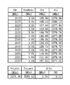
本発明者は、サンプルとして、二つの電圧制御発振器を選び、周波数変化幅を求め、2GHz帯のWCDMAにおいて、中間周波数をシンボルレートの整数倍にさせる局部発振周波数を求めてみた。図5Aは、第1のサンプルにおける周波数関係を示す表である。図5Bは、第2のサンプルにおける周波数関係を示す表である。図5Cは、第1および第2のサンプルについて、RF信号の受信周波数(RF受信周波数)と局部発振周波数との関係を示すグラフである。 The present inventor has selected two voltage controlled oscillators as samples, obtained a frequency change width, and obtained a local oscillation frequency that makes an intermediate frequency an integer multiple of a symbol rate in 2 GHz band WCDMA. FIG. 5A is a table showing the frequency relationship in the first sample. FIG. 5B is a table showing the frequency relationship in the second sample. FIG. 5C is a graph showing the relationship between the RF signal reception frequency (RF reception frequency) and the local oscillation frequency for the first and second samples.
2GHz帯のWCDMAにおいて、RF受信周波数fRFは、2110〜2170MHzである。シンボルレートSymRateは、3.84MHzである。第1のサンプルの電圧制御発振器の発振周波数fLOが、バラツキのため、2240MHz付近であったとする。このとき、局部発振周波数の最小値(fLo_min)が2237.96MHzであり、最大値(fLo_max)が2241.72MHzであったとする。したがって、周波数変化幅ΔfLOは、3.76MHzである。この周波数変化幅ΔfLoの中で、中間周波数fIFをシンボルレートの整数倍にすることができる局部発振周波数は、図5Aの上段の表に示すように、存在する。図5Aの上段の表に示すように、中間周波数fIFは、69.12〜130.56MHzの値をとる。このように、電圧制御発振器に要求される周波数範囲は、RF受信周波数fRFの中心周波数(2140MHz)の約0.17%で十分である。 In the 2 GHz band WCDMA, the RF reception frequency f RF is 2110 to 2170 MHz. The symbol rate SymRate is 3.84 MHz. It is assumed that the oscillation frequency f LO of the voltage controlled oscillator of the first sample is around 2240 MHz due to variations. At this time, it is assumed that the minimum value (f Lo — min) of the local oscillation frequency is 2237.96 MHz and the maximum value (f Lo — max) is 2241.72 MHz. Therefore, the frequency change width Δf LO is 3.76 MHz. Within this frequency change width Δf Lo , there are local oscillation frequencies that allow the intermediate frequency f IF to be an integral multiple of the symbol rate, as shown in the upper table of FIG. 5A. As shown in the upper table of FIG. 5A, the intermediate frequency f IF takes a value of 69.12 to 130.56 MHz. Thus, the frequency range required for the voltage controlled oscillator is sufficient in about 0.17% of the RF reception frequency f RF center frequency (2140 MHz).
第2のサンプルの電圧制御発振器の発振周波数fLOが、バラツキのため、2280MHz付近であったとする。このとき、局部発振周波数の最小値(fLo_min)が2276.36MHzであり、最大値(fLo_max)が2280.12MHzであったとする。したがって、周波数変化幅ΔfLOは、3.76MHzである。この周波数変化幅ΔfLoの中で、中間周波数fIFをシンボルレートの整数倍にすることができる局部発振周波数は、図5Bの上段の表に示すように、存在する。図5Aの上段の表に示すように、中間周波数fIFは、107.52〜168.96MHzの値をとる。このように、電圧制御発振器に要求される周波数範囲は、RF受信周波数fRFの中心周波数(2140MHz)の約0.17%で十分である。 It is assumed that the oscillation frequency f LO of the voltage-controlled oscillator of the second sample is around 2280 MHz due to variations. At this time, it is assumed that the minimum value (f Lo — min) of the local oscillation frequency is 2276.36 MHz and the maximum value (f Lo — max) is 2280.12 MHz. Therefore, the frequency change width Δf LO is 3.76 MHz. Within this frequency change width Δf Lo , there are local oscillation frequencies that allow the intermediate frequency f IF to be an integral multiple of the symbol rate, as shown in the upper table of FIG. 5B. As shown in the upper table of FIG. 5A, the intermediate frequency f IF has a value of 107.52 to 168.96 MHz. Thus, the frequency range required for the voltage controlled oscillator is sufficient in about 0.17% of the RF reception frequency f RF center frequency (2140 MHz).
ここで、比帯域が約0.17%であることの効果について説明しておく。通常、たとえば、2140MHzの発振周波数に対して、帯域幅は、60MHz+マージン分が必要である。したがって、比帯域としては、2.8%+αが必要である。従って、電圧制御発振器は、バンド数を増やして、制御電圧に対する周波数変化率の傾きを急にしなければならない。そのため、C/Nが劣化することとなるので、結果、消費電力が増大することとなる。しかし、本実施形態のように、比帯域が、約0.17%であれば、制御電圧に対する周波数変化率の傾きが緩やかでよい。そのため、C/Nが劣化が防止でき、結果、消費電力を低減することができる。 Here, the effect of the specific bandwidth being about 0.17% will be described. Usually, for example, for an oscillation frequency of 2140 MHz, the bandwidth needs 60 MHz + margin. Accordingly, 2.8% + α is necessary as the specific band. Therefore, the voltage-controlled oscillator has to increase the number of bands to make the slope of the frequency change rate with respect to the control voltage steep. For this reason, C / N deteriorates, and as a result, power consumption increases. However, if the ratio band is about 0.17% as in this embodiment, the slope of the frequency change rate with respect to the control voltage may be gentle. Therefore, deterioration of C / N can be prevented, and as a result, power consumption can be reduced.
RF受信周波数fRFが2110〜2170MHzのRF信号を受信する場合であっても、図5Cに示すように、約2240MHz〜約2280MHzの局部発振周波数を使用することができることが分かる。 As shown in FIG. 5C, it can be seen that a local oscillation frequency of about 2240 MHz to about 2280 MHz can be used even when an RF signal having an RF reception frequency f RF of 2110 to 2170 MHz is received.
このように、第1および第2のサンプルからも分かるように、本発明の構成では、電圧制御発振器は、周波数可変範囲が従来に比べ狭くてもよく、さらに、バラツキを有する局部発振周波数を有していたとしてもよい。したがって、局部発振周波数をバンド毎に不連続にすることができるので、局部発振器の低消費電力化が実現される。 Thus, as can be seen from the first and second samples, in the configuration of the present invention, the voltage-controlled oscillator may have a narrower frequency variable range than the conventional one, and further has a local oscillation frequency with variations. You may have done it. Therefore, since the local oscillation frequency can be made discontinuous for each band, the power consumption of the local oscillator can be reduced.
図6は、周波数変換器102の回路例を示す図である。図6に示すように、周波数変換器102は、ギルバートセルを用いたダブルバランスミキサをベースにして構成されている。キャパシタと抵抗とを並列に接続した帰還回路102A,102BをRF側に設けることによって、位相を補償した負帰還増幅器となるため、周波数変換可能な帯域を広帯域にすることができる。さらに、IF側に抵抗回路102Cを用いることによって、インダクタとは異なり、インピーダンスの周波数依存性のない負荷となるため、周波数変換可能な帯域を広帯域にすることができる。
FIG. 6 is a diagram illustrating a circuit example of the
図7Aは、復調器103の構成を示すブロック図である。図7Aにおいて、復調器103は、帯域通過フィルタ150と、アナログデジタル変換部(ADC:Analog Digital Converter)160と、チャネル選択部170とを含む。チャネル選択部170は、ミキシング部171と、チャネル選択用フィルタ部172と、クロック生成部173とを有する。ミキシング部171は、第1のデジタルミキサ174と、第2のデジタルミキサ175と、移相器176とを有する。チャネル選択用フィルタ部172は、第1のローパスフィルタ177と、第2のローパスフィルタ178とを有する。
FIG. 7A is a block diagram showing a configuration of
図7Bは、帯域通過フィルタ150に入力されるIF信号の周波数スペクトルを示す図である。図7Bでは、1〜3のチャネルがIF信号に含まれていると例示している。帯域通過フィルタ150は、受信したいバンドに対応するIF信号を全て通過させる。これによって、後段のアナログデジタル変換部160において、所望のIF信号の周波数と同じ周波数にエリアジングで折り返してくる雑音を低減することができる。図7Cは、帯域通過フィルタ150が通過させる帯域を示す図である。
FIG. 7B is a diagram illustrating a frequency spectrum of the IF signal input to the
アナログデジタル変換部160は、外部または内部からのサンプリング用クロック信号に基づいて、帯域通過フィルタ150が通過したIF信号をデジタル信号に変換する。ここで、サンプリング用クロック信号の周波数(サンプリング周波数)をfsと表記する。サンプリング周波数fsは、ナイキストのサンプリング定理よって、IF信号の周波数(中間周波数)の2倍以上の周波数でなければならない。さらに、サンプリング周波数fsは、シンボルレートの整数倍である。このように、中間周波数およびサンプリング周波数をシンボルレートの整数倍とすることによって、アナログデジタル変換部160は、容易に、IF信号をデジタル信号に変換することができる。
The analog-
チャネル選択部170は、アナログデジタル変換部160によって得られた当該デジタル信号から所望のチャネルを選択する。具体的には、チャネル選択部170において、当該デジタル信号は、2分岐され、第1および第2のデジタルミキサ174,175に入力される。クロック生成部173は、チャネル選択用クロック信号を出力する。クロック生成部173から出力されたチャネル選択用クロック信号は、移相器176において、0度位相が回転され、第1のデジタルミキサ174に入力されると共に、90度位相が回転され、第2のデジタルミキサ175に入力される。第1のデジタルミキサ174は、当該デジタル信号と0度位相が回転したチャネル選択用クロック信号とをミキシングして、所望のチャネルのIをベースバンドにダウンコンバートする。第2のデジタルミキサ175は、当該デジタル信号と90度位相が回転したチャネル選択用クロック信号とをミキシングして、所望のチャネルのQをベースバンドにダウンコンバートする。図7Dは、ミキシング部171によって、所望のチャネルがベースバンドにダウンコンバートされたときの様子を示す図である。そして、第1のローパスフィルタ177は、所望のチャネルのIのみを通過する。第2のローパスフィルタ178は、所望のチャネルのQのみを通過する。図7Eは、所望のチャネルのみが通過される様子を示す図である。なお、第1および第2のデジタルミキサ174,175、クロック生成部173、移相器176、ならびに第1および第2のローパスフィルタ177,178は、サンプリング用クロック信号に同期して動作する。
The
図8は、チャネル選択用のクロック生成部173の構成例を示すブロック図である。図8において、チャネル選択用クロック生成部173は、割り算部173−1〜173−7と、SPDT(single pole double throw)173−8〜173−14と、ミキシング部173−15〜173−20と、DPDT(double pole double throw)173−21〜173−26とを含む。ミキシング部173−15〜173−20は、それぞれ、f1およびf2が入力された場合、f1+f2を出力し、f1のみが入力された場合、f1のみを出力する。SPDT173−8〜173−14は、入力側端子が1つであり、出力側端子が2つであり、スイッチを切り換えることによって、1つの入力側端子と1つの出力側端子との接続を切り換えることができる。DPDT173−21〜173−26は、入力側端子が2つであり、出力側端子が2つであり、スイッチを切り換えることによって、ある1つの入力側端子とある1つの出力側端子とを接続することができる。
FIG. 8 is a block diagram illustrating a configuration example of the
サンプリング周波数fsは、シンボルレートの整数倍であるので、SPDT173−8〜173−14およびDPDT173−21〜173−26におけるスイッチの切り換えを適切に行うことによって、クロック生成部173は、シンボルレートの整数倍の周波数を有するチャネル選択用クロック信号を出力することができる。なお、たとえば、図5Aおよび図5Bに示すように、実際に使用する中間周波数は、狭い範囲となる(たとえば、約60MHz〜170MHz)ので、図8に示す回路構成は、さらに簡略化できる。なお、中間周波数が2倍のシンボルレートの整数倍であれば、さらに、回路を簡略化できる。同様に、中間周波数が、3倍、…、N倍のシンボルレートの整数倍であれば、回路を簡略化できる。
Since the sampling frequency fs is an integer multiple of the symbol rate, the
このように、第1の実施形態によれば、局部発振器101は、中間周波数をシンボルレートの整数倍にするような周波数を有する局部発振信号を出力する。中間周波数をシンボルレートの整数倍とすることによって、復調器103は、アナログデジタル変換を容易に実行することができ、かつ、所望のチャネルを容易に選択することができる。復調器において所望のチャネルが選択されるので、復調器の前段においては、バンドを選択するだけでよい。中間周波数をシンボルレートの整数倍にすることができる局部発振周波数は複数存在する。したがって、局部発振器101内の電圧制御発振器116にバラツキがあったとしても、そのような局部発振周波数を選択することは可能である。よって、電圧制御発振器116は、バンドに対応して、不連続にバンドを切り替えることができ、かつ、制御電圧に対して、緩やかに局部発振周波数が変化する特性を有してさえいればよい。先述したように、そのような電圧制御発振器116は、消費電力が従来に比べて少なくてよい。したがって、RFアナログの局部発振器の消費電力を低減しながらも、マルチバンドおよびマルチモードを実現することができる無線受信装置が提供されることとなる。
Thus, according to the first embodiment, the
(第1の実施形態における電圧制御発振器の変形例)
図9は、電圧制御発振器116の他の例を示す回路図である。図9において、図3に示す回路と同様の機能を有する部分については、同一の参照符号を付し、説明を省略する。図9に示す電圧制御発振器116は、可変容量回路1162の代わりに、微調整用スイッチ回路1162cを含む。微調整用スイッチ回路1162cは、複数のキャパシタのそれぞれにスイッチング素子が接続され、当該スイッチング素子のオンオフが制御されることによって、局部発振周波数を微調整する。図9に示す構成によって、微調整用の可変容量のQ値を高くできるので、電圧制御発振器116の低消費電力化を実現することができる。
(Modification of the voltage controlled oscillator in the first embodiment)
FIG. 9 is a circuit diagram showing another example of the voltage controlled
ここで、微調整用スイッチ回路1162cを用いて、シンボルレートの整数倍に中間周波数を合わせることができる理由について説明する。たとえば、周波数f0およびf0+Δfの2つをΔf/2の周期で切り換える場合を考える。この場合、出力信号S(t)は、以下のように表される。
S(t)=A(Δf/2)・cos2π(f0)t+B(Δf/2)・cos2π(f0+Δf)t
ここで、A(Δf/2)は、時刻1/Δf〜2/Δfまでが0で、それ以外が1の関数である。B(Δf/2)は、時刻1/Δf〜2/Δfまでが1で、それ以外が0の関数である。S(t)を計算すると、必ず、cos2π(f0+Δf/2)tの成分が現れてくる。したがって、適切にスイッチを切り換えることによって、2つの容量の中間の値を等価的に実現でき、連続的な周波数変化が可能となる。ゆえに、当該変形例を用いても、シンボルレートの整数倍に中間周波数を合わせることができる。
Here, the reason why the intermediate frequency can be adjusted to an integral multiple of the symbol rate by using the fine adjustment switch circuit 1162c will be described. For example, consider a case where two frequencies f0 and f0 + Δf are switched at a period of Δf / 2. In this case, the output signal S (t) is expressed as follows.
S (t) = A (Δf / 2) · cos2π (f0) t + B (Δf / 2) · cos2π (f0 + Δf) t
Here, A (Δf / 2) is a function of 0 from
(第1の実施形態における周波数変換器の変形例)
図10Aは、周波数変換器102の他の例を示す回路図である。図10Aに示す周波数変換器102は、サンプルホールド回路を用いたダウンコンバータである。ここでは、経路が4つの場合を示しているが、それに限られない。図10Aに示すダウンコンバータは、局部発振器101からの局部発振信号の局部発振周波数の4分の1のタイミングでサンプリングを行う。サンプリングが行われるタイミングは、4つの経路上で時間的にずれている。図10Bは、4つの経路に入力されるサンプリングのためのクロックLO/4_1,LO/4_2,LO/4_3,LO/4_4を示す図である。これにより、1つのスイッチの切換時間のスペックが緩和される。この構成により、時間方向にデジタル的にダウンコンバートが行われるため、比較的ばらつきが小さく、帯域の広いダウンコンバータが実現できる。
(Modification of the frequency converter in the first embodiment)
FIG. 10A is a circuit diagram illustrating another example of the
(第1の実施形態における復調器の第1の変形例)
図11Aは、復調器103の他の構成を示すブロック図である。図11Aにおいて、図7Aに示す構成と同様の機能を有する部分については、同一の参照符号を付し、詳しい説明を省略する。図11Aにおいて、復調器103は、帯域通過フィルタ150と、アナログデジタル変換部160と、チャネル選択部180とを含む。チャネル選択部180は、ミキシング部171と、チャネル選択用フィルタ181と、クロック生成部173とを有する。図11Bは、IF信号のスペクトルを示す図である。図11Cは、帯域通過フィルタ150による帯域通過の様子を示す図である。
(First Modification of Demodulator in First Embodiment)
FIG. 11A is a block diagram showing another configuration of the
図11Dは、チャネル選択用フィルタ181によるチャネル選択の様子を示す図である。チャネル選択用フィルタ181は、チャネル選択用のチューナブルバンドパスフィルタであって、所望のチャネルを通過することができる。チャネル選択用フィルタ181は、チューナブルバンドパスフィルタとして、FIRフィルタやIIRフィルタ等を用いる。これによって、タップの値を変更することによって、所望のチャネルを通過させることができる。特に、本発明では、中間周波数がシンボルレートの整数倍であるので、サンプリング周波数fsと入力されるデジタル信号との間の同期がとりやすい。したがって、比較的容易な回路構成で、精度の良いバンドパスフィルタを提供することができる。なお、この場合も、チャネル選択用のクロック生成部173として、図8に示す構成を適用することができる。
FIG. 11D is a diagram illustrating a state of channel selection by the
図11Eは、ミキシング部によって、所望のチャネルがベースバンドにダウンコンバートされたときの様子を示す図である。このように、図11Aに示す構成を用いても、所望のチャネルを選択することができる。 FIG. 11E is a diagram illustrating a state in which a desired channel is down-converted to baseband by the mixing unit. Thus, a desired channel can be selected even using the configuration shown in FIG. 11A.
(第1の実施形態における復調器の第2の変形例)
図12は、復調器103の他の構成を示すブロック図である。図12において、図7Aに示す構成と同様の機能を有する部分については、同一の参照符号を付し、詳しい説明を省略する。図12において、復調器103は、帯域通過フィルタ150と、アナログデジタル変換部160と、チャネル選択部190とを含む。チャネル選択部190は、デジタルフーリエ変換(DFT)部191と、周波数成分選択部192と、周波数シフト部193と、逆デジタルフーリエ変換部194とを含む。逆デジタルフーリエ変換部194は、実部虚部分岐部195と、第1の逆デジタルフーリエ変換部196と、第2の逆デジタルフーリエ変換部197と有する。
(Second Modification of Demodulator in First Embodiment)
FIG. 12 is a block diagram showing another configuration of the
デジタルフーリエ変換部191は、アナログデジタル変換部によって得られたデジタル信号をデジタルフーリエ変換して、f1〜fNの周波数成分に分解する。周波数成分選択部192は、所望のチャネルの再生に必要な周波数成分を少なくとも1つ選択する。当該選択は、パラレルに行われても良いし、シリアルに行われてもよい。周波数シフト部193は、周波数成分選択部192によって選択された周波数成分をベースバンド帯域にシフトする。実部虚部分岐部195は、周波数シフト部193からの出力を実数部と虚数部とに分岐する。実数部は、第1の逆デジタルフーリエ変換部196によって逆デジタルフーリエ変換されて、所望のチャネルのIが出力される。虚数部は、第2の逆デジタルフーリエ変換部197によって逆デジタルフーリエ変換されて、所望のチャネルのQが出力される。このように、逆デジタルフーリエ変換部194は、周波数成分選択部192によって選択され、周波数シフト部193によって周波数シフトされた1つの周波数成分を逆フーリエ変換することによって、所望のチャネルを選択する。
The digital
中間周波数は、シンボルレートの整数倍であるので、デジタル信号のデジタルフーリエ変換を容易に行うことができる。なぜなら、デジタル信号とシンボルレートとの同期がとりやすくなるからである。 Since the intermediate frequency is an integer multiple of the symbol rate, digital Fourier transform of the digital signal can be easily performed. This is because the digital signal and the symbol rate can be easily synchronized.
(第2の実施形態)
上記第1の実施形態では、イメージ妨害をRFのバンドパスフィルタで低減することとしたが、アプリケーションによっては、さらに、イメージ妨害を実現する必要がある。そこで、第2の実施形態を提案する。第2の実施形態では、周波数変換器の構成が第1の実施形態と異なる。
(Second Embodiment)
In the first embodiment, the image disturbance is reduced by the RF band-pass filter. However, depending on the application, it is necessary to further realize the image disturbance. Therefore, a second embodiment is proposed. In the second embodiment, the configuration of the frequency converter is different from that of the first embodiment.
図13は、本発明の第2の実施形態に係る周波数変換器202の構成を示すブロック図である。周波数変換器202以外は、第1の実施形態と同様である。図13において、周波数変換器202は、第1の移相器212と、第2の移相器222と、第1のダウンコンバータ232と、第2のダウンコンバータ242とを備える。
FIG. 13 is a block diagram showing the configuration of the
第1の移相器212は、局部発振器101から出力される局部発振信号の位相を0度回転させて第1のダウンコンバータ232に入力すると共に、90度回転させて第2のダウンコンバータ242に入力する。第1のダウンコンバータ232は、0度位相が回転した局部発振信号に基づいて、RF信号をダウンコンバートする。第2のダウンコンバータ242は、90度位相が回転した局部発振信号に基づいて、RF信号をダウンコンバートする。第2の移相器222は、第1のダウンコンバータ232の出力の位相を0度回転させ、第2のダウンコンバータ242の出力の位相を90度回転させて、得られる2つの信号を合成して、復調器103に入力する。
The
このように、第2の実施形態によれば、周波数変換器202は、ハートレー方式となるので、イメージ妨害を抑圧することができる。
As described above, according to the second embodiment, the
なお、局部発振器101は、所望の局部発振周波数の2N倍の周波数を有する局部発振信号を出力するようにして、分周器を用いて、0度・90度位相差を作ってもよい。
The
(第3の実施形態)
図14は、本発明の第3の実施形態に係る周波数変換器302の構成を示すブロック図である。図14において、第2の実施形態と同様の機能を有する部分については、同一の参照符号を付し、詳しい説明を省略する。周波数変換器302は、第1の移相器212と、第1のダウンコンバータ232と、第2のダウンコンバータ242とを含む。図14に示すように、0度・90度位相差を有する局部発振信号によって、RF信号はダウンコンバートされ、後述の図15Aに示す復調器403に入力される。
(Third embodiment)
FIG. 14 is a block diagram showing a configuration of a
図15Aは、復調器403の構成を示すブロック図である。復調器403は、第1の帯域通過フィルタ410と、第1のアナログデジタル変換部411と、第1のチャネル選択フィルタ412と、第1の合成部413と、第1のチャネル選択用クロック生成部416と、第3の移相器415と、第2の帯域通過フィルタ425と、第2のアナログデジタル変換部424と、第2のチャネル選択フィルタ423と、第2の合成部422と、第2のチャネル選択用クロック生成部419と、第4の移相器420とを含む。第1の合成部413は、第1のデジタルミキサ414と、第2のデジタルミキサ417とを有する。第2の合成部422は、第3のデジタルミキサ418と、第4のデジタルミキサ421とを有する。
FIG. 15A is a block diagram showing a configuration of
第1の帯域通過フィルタ410は、第1のダウンコンバータ232からの出力信号の内、受信したいバンドに対応する前記中間周波数信号を全て通過させる。第1のアナログデジタル変換部411は、シンボルレートの整数倍のサンプリング周波数を有するサンプリング用クロック信号に基づいて、第1の帯域通過フィルタ410通過したIF信号をデジタル信号に変換する。第2の帯域通過フィルタ425は、第2のダウンコンバータ242からの出力信号の内、受信したいバンドに対応する前記中間周波数信号を全て通過させる。第2のアナログデジタル変換部424は、シンボルレートの整数倍のサンプリング周波数を有するサンプリング用クロック信号に基づいて、第2の帯域通過フィルタ425通過したIF信号をデジタル信号に変換する。図15Bは、IF信号の周波数スペクトルを示す図である。図15Cは、第1および第2の帯域通過フィルタ410,425における帯域通過の様子を示す図である。
The first
第1のチャネル選択フィルタ412は、第1のアナログデジタル変換部411によって得られたデジタル信号から所望のチャネルの周波数を通過させる。第2のチャネル選択フィルタ423は、第2のアナログデジタル変換部424によって得られたデジタル信号から所望のチャネルの周波数を通過させる。図15Dは、第1および第2のチャネル選択フィルタ412,423によって所望のチャネルが通過する様子を示す図である。
The first
第1および第2のチャネル選択用クロック生成部416,419は、所望のチャネルをベースバンドにダウンコンバートするための第1および第2のチャネル選択用クロック信号を生成する。
First and second channel
第3の移相器415は、第1のチャネル選択用クロック生成部416からのチャネル選択用クロック信号の位相を0度回転させて出力すると共に、90度回転させて出力する。
The
第4の移相器420は、第2のチャネル選択用クロック生成部419からのチャネル選択用クロック信号の位相を−90度回転させて出力すると共に、0度回転させて出力する。
The
第1の合成部413は、第1のチャネル選択フィルタ412からの出力と第3の移相器415からの0度回転したチャネル選択用クロック信号とを第1のデジタルミキサ414によってミキシングすると共に、第2のチャネル選択フィルタ423からの出力と第3の移相器415からの90度回転したチャネル選択用クロック信号とを第2のデジタルミキサ417によってミキシングして、ミキシングによって得られた2つの信号を合成して、Iとして出力する。
The
第2の合成部422は、第2のチャネル選択フィルタ423からの出力と第4の移相器420からの0度回転したチャネル選択用クロック信号とを第4のデジタルミキサ421によってミキシングすると共に、第1のチャネル選択フィルタ412からの出力と第4の移相器420からの−90度回転したチャネル選択用クロック信号とを第3のデジタルミキサによってミキシングして、ミキシングによって得られた2つの信号を合成して、Qとして出力する。図15Eは、第1および第2の合成部413,422におけるベースバンドへのダウンコンバートの様子を示す図である。
The second synthesis unit 422 mixes the output from the second
このように、第3の実施形態では、イメージ周波数の抑圧がデジタル部で行われるため、イメージ周波数の抑圧の精度が向上する。また、合成を行う前に信号の振幅、位相の補正を行うことでさらにイメージ抑圧を改善することができる。 As described above, in the third embodiment, since image frequency suppression is performed by the digital unit, the accuracy of image frequency suppression is improved. Further, image suppression can be further improved by correcting the amplitude and phase of the signal before synthesis.
(第3の実施形態の復調器の第1の変形例)
図16は、第3の実施形態に係る復調器403の第1の変形例の構成を示すブロック図である。図16において、図15Aに示す部分と同様の機能を有する部分については、同一の参照符号を付し、詳しい説明を省略する。図16において、復調器403は、第1の帯域通過フィルタ410と、第1のアナログデジタル変換部411と、第1のチャネル選択フィルタ412と、第2の帯域通過フィルタ425と、第2のアナログデジタル変換部424と、第2のチャネル選択フィルタ423と、チャネル選択用クロック生成部430と、第1のデジタルダウンコンバータ431と、第2のデジタルダウンコンバータ432と、第3の移相器433と、第4の移相器434と、第1の合成部435と、第2の合成部436とを含む。
(First Modification of Demodulator of Third Embodiment)
FIG. 16 is a block diagram illustrating a configuration of a first modification of the
チャネル選択用クロック生成部430は、所望のチャネルをベースバンドにダウンコンバートするためのチャネル選択用クロック信号を生成する。第3の移相器433は、第1のチャネル選択フィルタ412からの出力の移相を−90度回転させる。第4の移相器434は、第2のチャネル選択用フィルタからの出力の移相を90度回転させる。第1の合成部435は、第3の移相器433からの出力と第2のチャネル選択フィルタ423からの出力とを合成する。第2の合成部436は、第4の移相器434からの出力と第1のチャネル選択フィルタ412からの出力とを合成する。第1のデジタルダウンコンバータ431は、第2の合成部436からの出力をチャネル選択用クロック信号によってダウンコンバートして、Iとして出力する。第2のデジタルダウンコンバータ432は、第1の合成部435からの出力をチャネル選択用クロック信号によってダウンコンバートして、Qとして出力する。
The channel selection
図16に示す構成によって、第1および第2の合成部435,436において、イメージ周波数が除去されることとなる。
With the configuration shown in FIG. 16, the image frequency is removed in the first and
(第3の実施形態における復調器の第2の変形例)
図17は、第3の実施形態における復調器403の第2の変形例の構成を示すブロック図である。図17において、図15Aに示す部分と同様の機能を有する部分については、同一の参照符号を付し、詳しい説明を省略する。図17において、復調器403は、第1の帯域通過フィルタ410と、第1のアナログデジタル変換部411と、第2の帯域通過フィルタ425と、第2のアナログデジタル変換部424と、第1のデジタルフーリエ変換部441と、第1の周波数成分選択部442と、第1の合成部443と、第1の乗算部445と、第1の周波数シフト部446と、第1の逆デジタルフーリエ変換部447と、第2のデジタルフーリエ変換部448と、第2の周波数成分選択部449と、第2の合成部451と、第2の乗算部450と、第2の周波数シフト部452と、第2の逆デジタルフーリエ変換部453とを含む。
(Second Modification of Demodulator in Third Embodiment)
FIG. 17 is a block diagram illustrating a configuration of a second modification of the
第1のデジタルフーリエ変換部441は、第1のアナログデジタル変換部411によって得られたデジタル信号をデジタルフーリエ変換する。第2のデジタルフーリエ変換部448は、第2のアナログデジタル変換部424によって得られたデジタル信号をデジタルフーリエ変換する。
The first digital
第1の周波数成分選択部442は、第1のデジタルフーリエ変換部によって得られた複数の周波数成分から、所望のチャネルを再生するのに必要な少なくとも1つの周波数成分を選択する。
The first frequency
第1の乗算部は、第1の周波数成分選択部442によって選択された少なくとも1つの周波数成分に対して、−j(jは虚数)を乗算する。
The first multiplier multiplies at least one frequency component selected by the first
第2の周波数成分選択部449は、第2のデジタルフーリエ変換部448によって得られた複数の周波数成分から、所望のチャネルを再生するのに必要な少なくとも1つの周波数成分を選択する。
The second frequency
第2の乗算部450は、第2の周波数成分選択部449によって選択された少なくとも1つの周波数成分に対して、j(jは虚数)を乗算する。
The
第1の合成部443は、第1の乗算部445の乗算結果と第2の周波数成分選択部449によって選択された少なくとも1つの周波数成分とを合成する。
The
第2の合成部451は、第2の乗算部450の乗算結果と第1の周波数成分選択部442によって選択された少なくとも1つの周波数成分とを合成する。
The
第1の周波数シフト部446は、第1の合成部443による合成結果をベースバンド帯域にシフトする。
The first
第2の周波数シフト部452は、第2の合成部451による合成結果をベースバンド帯域にシフトする。
The second
第1の逆デジタルフーリエ変換部447は、第1の周波数シフト部446によって周波数シフトされた少なくとも1つの周波数成分を逆デジタルフーリエ変換することによって、所望のチャネルを選択する。
The first inverse digital
第2の逆デジタルフーリエ変換部453は、第2の周波数シフト部452によって周波数シフトされた少なくとも1つの周波数成分を逆デジタルフーリエ変換することによって、所望のチャネルを選択する。
The second inverse digital
このように、第2の変形例では、第1および第2の合成部443,451において、イメージ周波数が除去されるので、イメージ妨害を抑圧する復調器が提供されることとなる。
As described above, in the second modification, the image frequency is removed in the first and
なお、復調器403は、イメージ周波数を除去するための構成を有していればよく、上記の構成に限定されるものではない。
The
(第4の実施形態)
第4の実施形態において、復調器の構成以外は、第1の実施形態と同様であるとする。図18Aは、本発明の第4の実施形態に係る復調器503の構成を示すブロック図である。図18Aにおいて、復調器503は、中心周波数可変帯域通過フィルタ513と、アナログデジタル変換部523と、チャネル選択部533とを含む。チャネル選択部533は、チャネル選択用クロック生成部543と、移相器553と、第1のデジタルミキサ563と、第2のデジタルミキサ573と、第1のローパスフィルタ583と、第2のローパスフィルタ593とを有する。図18Bは、1〜9のチャネルを含むIF信号の周波数スペクトルを示す図である。
(Fourth embodiment)
The fourth embodiment is the same as the first embodiment except for the configuration of the demodulator. FIG. 18A is a block diagram showing a configuration of a
中心周波数可変帯域通過フィルタ513は、通過帯域幅が1チャネルの帯域幅よりも大きくかつRF信号の1バンド当たりの帯域幅よりも小さく、通過帯域の中心周波数が可変なフィルタである。中心周波数可変帯域通過フィルタ513は、所望のチャネルが変わったら、通過帯域の中心周波数も変化させる。図18Cは、所望のチャネルが変わったときの通過帯域の中心周波数が変化する様子を示す図である。
The center frequency
アナログデジタル変換部523は、シンボルレートの整数倍のサンプリング周波数を有するサンプリング用クロック信号に基づいて、中心周波数可変帯域通過フィルタを通過したIF信号をデジタル信号に変換する。
The analog-to-
チャネル選択部533は、アナログデジタル変換部523によって得られたデジタル信号から所望のチャネルを選択する。図18Dは、チャネル選択部によって、所望のチャネルがベースバンドにダウンコンバートされたときの様子を示す図である。図18Eは、チャネル選択部によって、所望のチャネルが取り出されたときの様子を示す図である。チャネル選択部533の構成は、図7Aに示すように、第1の実施形態と同様であるので、詳しい動作説明を省略する。
The
このように、中心周波数可変帯域通過フィルタ513を用いることで、アナログデジタル変換部523に入力される妨害波のレベルを、中心周波数可変帯域通過フィルタ513によって、低減することができる。したがって、アナログデジタル変換部523のダイナミックレンジが低減し、低消費電力化を図ることができる。さらに、所望チャネルのみを通過させる従来の受信回路装置のIFフィルタと異なり、中心周波数のばらつきの許容範囲が大きくなるため、フィルタの中心周波数の調整回路が簡易化できる。
Thus, by using the center frequency
図19は、中心周波数可変帯域通過フィルタ513の構成例を示す図である。図19に示すように、中心周波数可変帯域通過フィルタ513は、可変容量および可変インダクタが並列に接続された並列共振器である。可変容量は、バラクタダイオードによって構成されている。可変インダクタは、オペアンプによって構成されている。バラクタダイオードの容量値とオペアンプの電流値とを変化させることによって、中心周波数可変帯域通過フィルタ513の中心周波数を制御することができる。
FIG. 19 is a diagram illustrating a configuration example of the center frequency
図20は、中心周波数可変帯域通過フィルタ513の中心周波数を調整するための構成を示す図である。復調器503は、さらに、中心周波数制御部601と、スイッチ回路602と、レベル検出部603と、オフセット制御部604とを含む。
FIG. 20 is a diagram illustrating a configuration for adjusting the center frequency of the center frequency
中心周波数制御部601は、所望のチャネルに応じて、中心周波数可変帯域通過フィルタ513の中心周波数を制御する。スイッチ回路602は、所定のタイミングに応じて、中心周波数可変帯域通過フィルタ513からの出力をレベル検出部603に入力するようにスイッチングする。レベル検出部603は、中心周波数可変帯域通過フィルタ513からの出力信号の電力レベルを検出する。
The center frequency control unit 601 controls the center frequency of the center frequency
オフセット制御部604は、いくつかのIF信号を用いて、中心周波数可変帯域通過フィルタ513の中心周波数のオフセットのキャリブレーションをとる。キャリブレーションをとる方法として、たとえば、無線受信装置は、未送信時に、送信回路605から、スイッチ回路606を介してIF信号を周波数変換器102に入力し、IF信号を作って、レベル検出部603の検出電力が最大となるようにオフセットを制御する。最初のキャリブレーションをとるとき以外、オフセット制御部604は、レベル検出部603の検出結果に基づいて、中心周波数可変帯域通過フィルタ513のオフセットを制御する。オフセット制御部604は、中心周波数可変帯域通過フィルタ513からの出力信号のレベルが最大となるように、オフセットを制御する。
The offset
以上により、固定の寄生成分の影響等によって、中心周波数がずれたとしても、オフセットを制御することによって、中心周波数のずれを補正(キャリブレーション)することができる。 As described above, even if the center frequency shifts due to the influence of a fixed parasitic component, the center frequency shift can be corrected (calibrated) by controlling the offset.
(第4の実施形態における中心周波数制御部の変形例)
図21Aは、第4の実施形態における中心周波数可変帯域通過フィルタ513の変形例を示す回路図である。図21Aに示すように、中心周波数可変帯域通過フィルタ513は、少なくとも2つのスイッチング素子と少なくとも1つのキャパシタとを有するスイッチドキャパシタ回路であって、一方のスイッチング素子の切り換え周期を変化させることによって、中心周波数を変化させることができる。
(Modification of the center frequency control unit in the fourth embodiment)
FIG. 21A is a circuit diagram showing a modification of the center frequency
図21Bは、図21Aにおける主要部の信号の時間変化を示す図である。図21Bに示すように、周波数の異なる2つの信号signal1(点線)とsignal2(実線)とが入力端子INに入力されたとする。signal1の周波数の信号が入力された場合、出力端子OUTにsignal1の信号が現れる。一方、signal2の周波数の信号が入力された場合、出力端子OUTには信号が現れない。clock2の周波数を変えることにより、通過周波数は変化する。
FIG. 21B is a diagram showing a time change of signals of main parts in FIG. 21A. As shown in FIG. 21B, it is assumed that two signals signal1 (dotted line) and signal2 (solid line) having different frequencies are input to the input terminal IN. When a signal having the frequency of signal1 is input, the signal of signal1 appears at the output terminal OUT. On the other hand, when a signal having a frequency of
以上のような構成により、離散時間のアナログチューナブルフィルタとして、中心周波数可変帯域通過フィルタ513を実現することができる。中心周波数可変帯域通過フィルタ513は、主にスイッチとキャパシタとで構成されるので、素子の非線形性の影響を受けにくいフィルタが実現できる。
With the above configuration, the center frequency
(第5の実施形態)
第1の実施形態では、サンプリング周波数fsは、IF信号の周波数の2倍以上であるとしていた。第5の実施形態では、サンプリング周波数fsが、IF信号の2倍未満の復調器を提案する。なお、第1の実施形態同様、サンプリング周波数fsは、シンボルレートの整数倍である。
(Fifth embodiment)
In the first embodiment, the sampling frequency fs is twice or more the frequency of the IF signal. In the fifth embodiment, a demodulator having a sampling frequency fs less than twice the IF signal is proposed. Note that the sampling frequency fs is an integer multiple of the symbol rate, as in the first embodiment.
図22Aは、本発明の第5の実施形態における復調器703の構成を示すブロック図である。第5の実施形態に係る無線受信装置において、復調器703以外は、第1の実施形態と同様の構成を有する。図22Aにおいて、復調器703は、帯域通過フィルタ710と、アナログデジタル変換部720と、チャネル選択部730とを含む。チャネル選択部730の構成は、第1の実施形態におけるチャネル選択部170と同様である。
FIG. 22A is a block diagram showing a configuration of a
アナログデジタル変換部720は、入力されたIF信号全てを、0〜fs/2Hzの間に折り返しながら、デジタル信号に変換する。したがって、周波数変換器102によってダウンコンバートされたIF信号の全てのチャネルが、N×fs/2以上、(N+1)×fs/2以下の周波数範囲に入るように、局部発振器101は、局部発振周波数を選ぶ。このように、アンダーサンプリングのために適切な局部発振周波数を選ぶと、アナログデジタル変換部720は、入力されたIF信号全てを、0〜fs/2Hzの間に折り返しながら、デジタル信号に変換することができる。
The analog-to-
図22Bは、帯域通過フィルタ710の通過特性を示す図である。帯域通過フィルタ710は、N×fs/2未満および(N+1)×fs/2を超える周波数帯域を十分に低減できる通過特性を有する。
FIG. 22B is a diagram illustrating a pass characteristic of the
図22Cは、アナログデジタル変換部720から出力されるデジタル信号のスペクトルを示す図である。図22Cに示すように、アナログデジタル変換部720から出力されるデジタル信号は、0〜fs/2Hzの周波数帯にダウンコンバートされている。したがって、チャネル選択部において、ベースバンド帯域にデジタル信号をダウンコンバートするためのクロック周波数を下げることができる。図22Dは、所望のチャネルをチャネル選択部730において、バースバンド帯域にダウンコンバートしたときの様子を示す図である。図22Eは、チャネル選択部730において、所望のチャネルを通過させる様子を示す図である。
FIG. 22C is a diagram illustrating a spectrum of a digital signal output from the analog-
以上、第5の実施形態では、ベースバンド帯域にデジタル信号をダウンコンバートするためのクロック周波数を下げることができるので、低消費電力化が図られる。 As described above, in the fifth embodiment, since the clock frequency for down-converting the digital signal to the baseband band can be lowered, the power consumption can be reduced.
(第6の実施形態)
図23Aは、本発明の第6の実施形態に係る周波数変換器102の構成を示す回路図である。図23Bは、図23Aに示す端子LO/4_1〜LO/4_4に入力されるクロックを示す図である。
(Sixth embodiment)
FIG. 23A is a circuit diagram showing a configuration of a
周波数変換器102は、第1のスイッチ102aと、第2のスイッチ102bと、第3のスイッチ102cと、第1のキャパシタ102dと、第2のキャパシタ102eとを1単位の回路として、当該回路を4つ備える。複数の第3のスイッチ102cは、同時にオンオフされるように接続されている。RF信号は、入力端子INから、第1のスイッチ102aに入力される。第1のスイッチ102aの出力信号は、第2のスイッチ102bに入力される。第2のスイッチ102bの出力信号は、復調器に入力される。第1のキャパシタ102dは、第1のスイッチ102aと第2のスイッチ102bとの接続端と、接地との間に挿入されている。第2のキャパシタ102eと第3のスイッチ102cとは、第1のスイッチ102aと第2のスイッチ102bとの接続端と、接地との間に直列に挿入されている。図23Bに示すように、第1のスイッチ102aは、局部発振器101の出力信号の周波数に応じてオンオフする。NOT回路によって、第2のスイッチ102bは、第1のスイッチがオンのときオフ、オフのときオンとなる。第3のスイッチ102cは、無線周波数信号の周波数帯に対応してオンオフする。
The
本発明の無線受信装置は、マルチバンドに対応しなければならないので、周波数変換器102にも、広帯域特性が要求される。図10Aに示した周波数変換器102では、電荷をホールドする容量値が固定となっている。しかし、ホールドすべき容量値は、周波数に応じて、適切な値に決められる。そこで、図23Aに示す周波数変換器102では、使用するバンド、f1(たとえば800MHz)またはf2(たとえば2GHz)に応じて、複数の第3のスイッチ102cを同時にオンオフすることによって、ホールドすべき容量値を変更することができる。周波数の低いf1では、容量値を大きくするために、複数の第3のスイッチ102cは、オンされる。周波数が高いf2では、容量値を小さくするために、複数の第3のスイッチ102cは、オフされる。このような構成にすることによって、ホールドすべき容量値をバンドに応じて切り換えることができるので、周波数変換回路102の広帯域化が実現される。
Since the radio reception apparatus of the present invention must support multiband, the
なお、ここでは、切り換えられるバンドが2つであるとしたが、3つ以上であてもよい。その場合、バンドに対応してスイッチの数が増加する回路構成となる。 Here, although two bands are switched, three or more bands may be used. In that case, the circuit configuration increases the number of switches corresponding to the band.
(第7の実施形態)
図24Aは、本発明の第7の実施形態に係る復調器103の構成を示すブロック図である。図24Aにおいて、第7の実施形態に係る復調器103は、帯域通過フィルタ150の構成に特徴がある。図24Bは、図24Aに示す帯域通過フィルタ150の構成を示す回路図である。図24Bにおいて、帯域通過フィルタ150は、複数のスイッチドキャパシタが並列に接続された離散時間フィルタによって構成される。図24Bにおいては、スイッチドキャパシタは、9並列に接続されている。
(Seventh embodiment)
FIG. 24A is a block diagram showing a configuration of the
図25は、帯域通過フィルタ150の周波数レスポンスを表す図である。図25において、横軸は周波数軸であり、fclockは、帯域通過フィルタ150をオン、オフする周波数を示し、fsumplingは、アナログデジタル変換部160のサンプリング周波数を示す。fsumplingとfclockとの間には、(式1)の関係が成り立つ。図25に示すように、帯域通過フィルタ150は、スイッチ1から順にオン、オフを繰り返すことで、後段のアナログデジタル変換部160から、所望のIF信号の周波数と同じ周波数にエリアジングで折り返してくる周波数を抑圧する。
fsumpling=1/2・fclock ・・・(式1)
FIG. 25 is a diagram illustrating a frequency response of the
f sumpling = 1/2 · f clock (Formula 1)
なお、帯域通過フィルタ150は、9並列の構成に限定されるわけでなく、受信したいバンドに対応するIF信号を通過させ、所望のIF信号の周波数と同じ周波数にエリアジングで折り返してくる周波数を抑圧するように構成すればよい。
The band-
このように、第7の実施形態では、帯域通過フィルタ150を最適に設計された離散時間フィルタによって構成することで、所望のIF信号の周波数と同じ周波数にエリアジングで折り返してくる周波数を効果的に抑圧することができる。
As described above, in the seventh embodiment, the band-
本発明の無線受信装置は、移動体端末、特にマルチモード、マルチバンドの移動体端末等への利用に適している。 The radio reception apparatus of the present invention is suitable for use in mobile terminals, in particular, multimode and multiband mobile terminals.
100 無線受信装置
101 局部発振器
102 周波数変換器
102A,102B 帰還回路
102C 抵抗回路
102a 第1のスイッチ
102b 第2のスイッチ
102c 第3のスイッチ
102d 第1のキャパシタ
102e 第2のキャパシタ
103 復調器
104 逆デジタルフーリエ変換部
105 帯域通過フィルタ
110 PLL回路
112 分周器
114 チャージポンプ
115 ローパスフィルタ
116 電圧制御発振器
117 プリスケーラ
118 可変分周器
120 検出部
130 判定部
140 周波数制御部
150 帯域通過フィルタ
160 アナログデジタル変換部
170 チャネル選択部
171 ミキシング部
172 チャネル選択用フィルタ部
173 クロック生成部
174 第1のデジタルミキサ
175 第2のデジタルミキサ
176 移相器
177 第1のローパスフィルタ
178 第2のローパスフィルタ
180 チャネル選択部
181 チャネル選択用フィルタ
190 チャネル選択部
191 デジタルフーリエ変換部
192 周波数成分選択部
193 周波数シフト部
194 逆デジタルフーリエ変換部
195 実部虚部分岐部
196 第1の逆デジタルフーリエ変換部
197 第2の逆デジタルフーリエ変換部
202 周波数変換器
212 第1の移相器
222 第2の移相器
232 第1のダウンコンバータ
242 第2のダウンコンバータ
302 周波数変換器
403 復調器
410 第1の帯域通過フィルタ
411 第1のアナログデジタル変換部
412 第1のチャネル選択フィルタ
413 第1の合成部
414 第1のデジタルミキサ
415 第3の移相器
416 第1のチャネル選択用クロック生成部
417 第2のデジタルミキサ
418 第3のデジタルミキサ
419 第2のチャネル選択用クロック生成部
420 第4の移相器
421 第4のデジタルミキサ
422 第2の合成部
423 第2のチャネル選択フィルタ
424 第2のアナログデジタル変換部
425 第2の帯域通過フィルタ
430 チャネル選択用クロック生成部
431 第1のデジタルダウンコンバータ
432 第2のデジタルダウンコンバータ
433 第3の移相器
434 第4の移相器
435 第1の合成部
436 第2の合成部
441 第1のデジタルフーリエ変換部
442 第1の周波数成分選択部
443 第1の合成部
445 第1の乗算部
446 第1の周波数シフト部
447 第1の逆デジタルフーリエ変換部
448 第2のデジタルフーリエ変換部
449 第2の周波数成分選択部
450 第2の乗算部
451 第2の合成部
452 第2の周波数シフト部
453 第2の逆デジタルフーリエ変換部
503 復調器
513 中心周波数可変帯域通過フィルタ
523 アナログデジタル変換部
533 チャネル選択部
543 チャネル選択用クロック生成部
553 移相器
563 第1のデジタルミキサ
573 第2のデジタルミキサ
583 第1のローパスフィルタ
593 第2のローパスフィルタ
601 中心周波数制御部
602 スイッチ回路
603 レベル検出部
604 オフセット制御部
605 送信回路
606 スイッチ回路
703 復調器
710 帯域通過フィルタ
720 アナログデジタル変換部
730 チャネル選択部
1161 インダクタ回路
1162 可変容量回路
1162a,1162b バラクタダイオード
1162c 微調整用スイッチ回路
1163 負性抵抗回路
1164 バンド切り換え用スイッチ回路
100 wireless receiver 101 local oscillator 102 frequency converter 102A, 102B feedback circuit 102C resistance circuit 102a first switch 102b second switch 102c third switch 102d first capacitor 102e second capacitor 103 demodulator 104 inverse digital Fourier transform unit 105 Band pass filter 110 PLL circuit 112 Frequency divider 114 Charge pump 115 Low pass filter 116 Voltage controlled oscillator 117 Prescaler 118 Variable frequency divider 120 Detection unit 130 Determination unit 140 Frequency control unit 150 Band pass filter 160 Analog to digital conversion unit 170 Channel selection unit 171 Mixing unit 172 Channel selection filter unit 173 Clock generation unit 174 First digital mixer 175 Second digital mixer 176 Phase shifter 17 First low-pass filter 178 Second low-pass filter 180 Channel selection unit 181 Channel selection filter 190 Channel selection unit 191 Digital Fourier transform unit 192 Frequency component selection unit 193 Frequency shift unit 194 Inverse digital Fourier transform unit 195 Real part Imaginary part branching unit 196 first inverse digital Fourier transform unit 197 second inverse digital Fourier transform unit 202 frequency converter 212 first phase shifter 222 second phase shifter 232 first down converter 242 second down converter 302 frequency Converter 403 Demodulator 410 First bandpass filter 411 First analog-to-digital converter 412 First channel selection filter 413 First combiner 414 First digital mixer 415 Third phase shifter 416 First Channel selection clock generator 4 7 Second digital mixer 418 Third digital mixer 419 Second channel selection clock generation section 420 Fourth phase shifter 421 Fourth digital mixer 422 Second synthesis section 423 Second channel selection filter 424 second 2 analog-digital conversion unit 425 second band pass filter 430 channel selection clock generation unit 431 first digital down converter 432 second digital down converter 433 third phase shifter 434 fourth phase shifter 435 first 1 synthesis unit 436 second synthesis unit 441 first digital Fourier transform unit 442 first frequency component selection unit 443 first synthesis unit 445 first multiplication unit 446 first frequency shift unit 447 first inverse Digital Fourier transform unit 448 Second digital Fourier transform unit 449 Second frequency component selection unit 45 Second multiplication unit 451 Second synthesis unit 452 Second frequency shift unit 453 Second inverse digital Fourier transform unit 503 Demodulator 513 Center frequency variable bandpass filter 523 Analog digital conversion unit 533 Channel selection unit 543 For channel selection Clock generation unit 553 Phase shifter 563 First digital mixer 573 Second digital mixer 583 First low pass filter 593 Second low pass filter 601 Center frequency control unit 602 Switch circuit 603 Level detection unit 604 Offset control unit 605 Transmission circuit 606 Switch circuit 703 Demodulator 710 Band pass filter 720 Analog to digital converter 730 Channel selector 1161 Inductor circuit 1162 Variable capacitance circuits 1162a and 1162b Varactor diode 1162c Fine adjustment switch times 1163 negative resistance circuit 1164 band switching switch circuit
Claims (24)
受信すべき前記無線周波数信号の周波数帯に対応する局部発振信号のバンドを、前記周波数帯に応じて不連続に切り換えて、前記局部発振信号を出力する局部発振器と、
前記局部発振器から出力される前記局部発振信号によって、前記無線周波数信号を前記中間周波数信号に変換して出力する周波数変換器と、
前記周波数変換器から出力される前記中間周波数信号を復調する復調器とを備え、
前記局部発振器は、前記周波数帯における前記局部発振信号の周波数変化幅を検出し、前記周波数変化幅の周波数の中から、シンボルレートの整数倍となる周波数を求め、前記中間周波数信号における受信すべきチャネルの中心周波数を前記シンボルレートの整数倍の周波数にさせるための局部発振周波数を有する前記局部発振信号を出力する、無線受信装置。A radio receiving apparatus that converts a received radio frequency signal into an intermediate frequency signal and demodulates the signal,
A local oscillator that switches the band of the local oscillation signal corresponding to the frequency band of the radio frequency signal to be received discontinuously according to the frequency band, and outputs the local oscillation signal;
A frequency converter that converts the radio frequency signal into the intermediate frequency signal by the local oscillation signal output from the local oscillator;
A demodulator that demodulates the intermediate frequency signal output from the frequency converter,
The local oscillator detects a frequency change width of the local oscillation signal in the frequency band, obtains a frequency that is an integral multiple of a symbol rate from the frequencies of the frequency change width, and should receive the intermediate frequency signal A radio receiving apparatus that outputs the local oscillation signal having a local oscillation frequency for making a center frequency of a channel an integer multiple of the symbol rate.
バンド切り換え機能を有する電圧制御発振器から出力される信号を前記局部発振信号として固定するためのPLL(Phase Locked Loop)回路と、
前記局部発振信号のバンドが切り換えられたら、前記電圧制御発振器から出力される信号をスイープさせる周波数制御部と、
前記周波数制御部によるスイープの結果に基づいて、前記周波数変化幅を検出する検出部と、
前記検出部によって検出された前記周波数変化幅の中から、シンボルレートの整数倍となる周波数を判定する判定部とを含み、
前記周波数制御部は、前記判定部によって判定された前記シンボルレートの整数倍の周波数に基づいて、前記PLL回路から出力される前記局部発振信号の前記局部発振周波数を制御する、請求項1に記載の無線受信装置。The local oscillator is
A PLL (Phase Locked Loop) circuit for fixing a signal output from a voltage controlled oscillator having a band switching function as the local oscillation signal;
When the band of the local oscillation signal is switched, a frequency control unit that sweeps the signal output from the voltage controlled oscillator;
Based on the result of the sweep by the frequency control unit, a detection unit for detecting the frequency change width,
A determination unit that determines a frequency that is an integral multiple of a symbol rate from the frequency change width detected by the detection unit;
The frequency control unit controls the local oscillation frequency of the local oscillation signal output from the PLL circuit based on a frequency that is an integral multiple of the symbol rate determined by the determination unit. Wireless receiver.
前記検出部は、前記PLL回路に含まれるチャージポンプの電圧に基づいて、前記周波数変化幅を検出する、請求項2に記載の無線受信装置。The frequency control unit controls the local oscillation frequency by controlling a frequency dividing number of a variable frequency divider included in the PLL circuit;
The radio reception apparatus according to claim 2, wherein the detection unit detects the frequency change width based on a voltage of a charge pump included in the PLL circuit.
キャパシタの接続数を切り換えることによって、前記局部発振信号のバンドを切り換えるためのスイッチ回路と、
前記局部発振信号の周波数を前記周波数変化幅の範囲で変化させるためのバラクタダイオード有する可変容量回路とを含む、請求項2に記載の無線受信装置。The voltage controlled oscillator is:
A switch circuit for switching the band of the local oscillation signal by switching the number of capacitors connected;
The wireless reception device according to claim 2, further comprising: a variable capacitance circuit having a varactor diode for changing the frequency of the local oscillation signal within a range of the frequency change width.
キャパシタの接続数を切り換えることによって、前記局部発振信号のバンドを切り換えるための第1のスイッチ回路と、
キャパシタの接続数を切り換えることによって、前記局部発振信号の周波数を前記周波数変化幅の範囲で変化させるための第2のスイッチ回路とを有する、請求項2に記載の無線受信装置。The voltage controlled oscillator is:
A first switch circuit for switching a band of the local oscillation signal by switching the number of capacitors connected;
The radio receiving apparatus according to claim 2, further comprising: a second switch circuit configured to change a frequency of the local oscillation signal in a range of the frequency change width by switching a number of capacitors connected.
受信したいバンドに対応する前記中間周波数信号を全て通過させる帯域通過フィルタと、
前記シンボルレートの整数倍のサンプリング周波数を有するサンプリング用クロック信号に基づいて、前記帯域通過フィルタを通過した前記中間周波数信号をデジタル信号に変換するアナログデジタル変換部と、
前記アナログデジタル変換部によって得られた前記デジタル信号から所望のチャネルを選択するチャネル選択部とを含む、請求項1に記載の無線受信装置。The demodulator
A bandpass filter that passes all the intermediate frequency signals corresponding to the band to be received;
An analog-to-digital converter that converts the intermediate frequency signal that has passed through the band-pass filter into a digital signal based on a sampling clock signal having a sampling frequency that is an integer multiple of the symbol rate;
The radio reception apparatus according to claim 1, further comprising: a channel selection unit that selects a desired channel from the digital signal obtained by the analog-digital conversion unit.
前記アナログデジタル変換部から出力される前記デジタル信号の内、所望のチャネルをベースバンドにダウンコンバートするためのチャネル選択用クロック信号を生成するクロック生成部と、
前記クロック生成部によって生成された前記チャネル選択用クロック信号と前記アナログデジタル変換部によって得られた前記デジタル信号とをミキシングして、所望のチャンネルをベースバンド帯域にダウンコンバートするミキシング部と、
前記ミキシング部によるミキシング後の前記デジタル信号から、所望のチャンネルのみを通過させるチャネル選択用フィルタ部とを含む、請求項6に記載の無線受信装置。The channel selector
A clock generation unit that generates a channel selection clock signal for down-converting a desired channel to a baseband among the digital signals output from the analog-digital conversion unit;
Mixing the channel selection clock signal generated by the clock generation unit and the digital signal obtained by the analog-to-digital conversion unit, and down-converting a desired channel to a baseband;
The radio reception apparatus according to claim 6, further comprising: a channel selection filter unit that allows only a desired channel to pass from the digital signal after mixing by the mixing unit.
前記サンプリング用クロック信号に基づいて、前記アナログデジタル変換部によって得られた前記デジタル信号から、所望のチャネルを選択するチャネル選択用フィルタ部と、
前記チャネル選択用フィルタ部によって選択された前記所望のチャネルの前記デジタル信号をベースバンド帯域にダウンコンバートするためのチャネル選択用クロック信号を生成するクロック生成部と、
前記クロック生成部によって生成された前記チャネル選択用クロック信号と前記アナログデジタル変換部によって得られた前記デジタル信号とをミキシングして、所望のチャンネルをベースバンドにダウンコンバートするミキシング部とを含む、請求項6に記載の無線受信装置。The channel selector
A channel selection filter unit that selects a desired channel from the digital signal obtained by the analog-to-digital conversion unit based on the sampling clock signal;
A clock generation unit that generates a channel selection clock signal for down-converting the digital signal of the desired channel selected by the channel selection filter unit into a baseband band;
A mixing unit that mixes the clock signal for channel selection generated by the clock generation unit and the digital signal obtained by the analog-to-digital conversion unit, and down-converts a desired channel to a baseband. Item 7. The wireless receiving device according to Item 6.
前記アナログデジタル変換部によって得られた前記デジタル信号をデジタルフーリエ変換するためのデジタルフーリエ変換部と、
前記デジタルフーリエ変換部によって得られた周波数成分を少なくとも1つ選択する周波数成分選択部と、
前記周波数成分選択部によって選択された前記少なくとも1つの周波数成分をベースバンド帯域にシフトする周波数シフト部と、
前記周波数シフト部によって周波数シフトされた前記少なくとも1つの周波数成分を逆デジタルフーリエ変換することによって、所望のチャネルを選択する逆デジタルフーリエ変換部とを含む、請求項6に記載の無線受信装置。The channel selector
A digital Fourier transform unit for digital Fourier transforming the digital signal obtained by the analog-digital conversion unit;
A frequency component selection unit that selects at least one frequency component obtained by the digital Fourier transform unit;
A frequency shift unit that shifts the at least one frequency component selected by the frequency component selection unit to a baseband;
The radio reception apparatus according to claim 6, further comprising: an inverse digital Fourier transform unit that selects a desired channel by performing an inverse digital Fourier transform on the at least one frequency component frequency-shifted by the frequency shift unit.
前記アナログデジタル変換部は、帯域通過フィルタを通過した前記中間周波数信号の全てを、サンプリング周波数の2分の1の周波数を有するデジタル信号に変換する、請求項6に記載の無線受信装置。The sampling frequency is less than twice the center frequency of the channel to be received in the intermediate frequency signal;
The radio reception apparatus according to claim 6, wherein the analog-to-digital conversion unit converts all of the intermediate frequency signals that have passed through a band-pass filter into digital signals having a frequency that is half of a sampling frequency.
前記中間周波数信号は、サンプリング周波数の2分の1のN倍(Nは1以上の整数)以上、サンプリング周波数の2分の1の(N+1)倍以下の周波数を有する、請求項6に記載の無線受信装置。The sampling frequency is less than twice the center frequency of the channel to be received in the intermediate frequency signal,
7. The intermediate frequency signal according to claim 6, wherein the intermediate frequency signal has a frequency not less than N times half of the sampling frequency (N is an integer of 1 or more) and not more than half (N + 1) times of the sampling frequency. Wireless receiver.
通過帯域幅が1チャネルの帯域幅よりも大きくかつ前記無線周波数信号の1バンド当たりの帯域幅よりも小さく、通過帯域の中心周波数が可変な中心周波数可変帯域通過フィルタと、
前記シンボルレートの整数倍のサンプリング周波数を有するサンプリング用クロック信号に基づいて、前記中心周波数可変帯域通過フィルタを通過した前記中間周波数信号をデジタル信号に変換するアナログデジタル変換部と、
前記アナログデジタル変換部によって得られた前記デジタル信号から所望のチャネルを選択するチャネル選択部とを含む、請求項1に記載の無線受信装置。The demodulator
A center frequency variable bandpass filter having a passband width larger than the bandwidth of one channel and smaller than the bandwidth per band of the radio frequency signal, and the center frequency of the passband being variable;
An analog-to-digital converter that converts the intermediate frequency signal that has passed through the center frequency variable bandpass filter into a digital signal based on a sampling clock signal having a sampling frequency that is an integer multiple of the symbol rate;
The radio reception apparatus according to claim 1, further comprising: a channel selection unit that selects a desired channel from the digital signal obtained by the analog-digital conversion unit.
前記中心周波数可変帯域通過フィルタからの出力信号の電力レベルを検出するレベル検出部と、
前記レベル検出部の検出結果に基づいて、前記中心周波数可変帯域通過フィルタのオフセットを制御するオフセット制御部とを含み、
前記オフセット制御部は、前記中心周波数可変帯域通過フィルタからの出力信号のレベルが最大となるように、前記オフセットを制御する、請求項12に記載の無線受信装置。The demodulator further comprises:
A level detector for detecting the power level of the output signal from the center frequency variable bandpass filter;
An offset control unit that controls an offset of the center frequency variable bandpass filter based on a detection result of the level detection unit,
The radio reception apparatus according to claim 12, wherein the offset control unit controls the offset so that a level of an output signal from the center frequency variable bandpass filter is maximized.
前記局部発振器から出力される前記局部発振信号の位相を0度回転させて第1の信号とし、90回転させて第2の信号とする第1の移相器と、
前記第1の信号に基づいて、前記無線周波数信号をダウンコンバートする第1のダウンコンバータと、
前記第2の信号に基づいて、前記無線周波数信号をダウンコンバートする第2のダウンコンバータと、
前記第1のダウンコンバータの位相を0度回転させて、前記第2のダウンコンバータの位相を90度回転させて、得られる2つの信号を合成して、前記復調器に入力する第2の移相器とを含む、請求項1に記載の無線受信装置。The frequency converter is
A first phase shifter that rotates the phase of the local oscillation signal output from the local oscillator by 0 degrees to become a first signal and rotates by 90 degrees to become a second signal;
A first downconverter that downconverts the radio frequency signal based on the first signal;
A second downconverter for downconverting the radio frequency signal based on the second signal;
The phase of the first down-converter is rotated by 0 degrees, the phase of the second down-converter is rotated by 90 degrees, the two obtained signals are combined, and the second shift input to the demodulator. The wireless receiver according to claim 1, comprising a phaser.
前記局部発振器から出力される前記局部発振信号の位相を0度回転させて第1の信号とし、90回転させて第2の信号とする移相器と、
前記第1の信号に基づいて、前記無線周波数信号をダウンコンバートして前記復調器に入力する第1のダウンコンバータと、
前記第2の信号に基づいて、前記無線周波数信号をダウンコンバートして前記復調器に入力する第2のダウンコンバータとを含み、
前記復調器は、イメージ周波数を除去するための構成を有する、請求項1に記載の無線受信装置。The frequency converter is
A phase shifter that rotates the phase of the local oscillation signal output from the local oscillator by 0 degrees to be the first signal, and rotates by 90 degrees to be the second signal;
A first downconverter that downconverts the radio frequency signal based on the first signal and inputs the signal to the demodulator;
A second down-converter that down-converts the radio frequency signal based on the second signal and inputs the signal to the demodulator;
The radio receiver according to claim 1, wherein the demodulator has a configuration for removing an image frequency.
前記第1のダウンコンバータからの出力信号の内、受信したいバンドに対応する前記中間周波数信号を全て通過させる第1の帯域通過フィルタと、
前記シンボルレートの整数倍のサンプリング周波数を有するサンプリング用クロック信号に基づいて、前記第1の帯域通過フィルタを通過した前記中間周波数信号をデジタル信号に変換する第1のアナログデジタル変換部と、
前記第1のアナログデジタル変換部によって得られた前記デジタル信号から所望のチャネルを選択する第1のチャネル選択フィルタと、
前記第2のダウンコンバータからの出力信号の内、受信したいバンドに対応する前記中間周波数信号を全て通過させる第2の帯域通過フィルタと、
前記シンボルレートの整数倍のサンプリング周波数を有するサンプリング用クロック信号に基づいて、前記第2の帯域通過フィルタを通過した前記中間周波数信号をデジタル信号に変換する第2のアナログデジタル変換部と、
前記第2のアナログデジタル変換部によって得られた前記デジタル信号から所望のチャネルを選択する第2のチャネル選択フィルタと、
所望のチャネルをベースバンドにダウンコンバートするための第1および第2のチャネル選択用クロック信号を生成するチャネル選択用クロック生成部と、
前記第1のチャネル選択用クロック信号の位相を0度回転させて出力すると共に、90度回転させて出力する第3の移相器と、
前記第2のチャネル選択用クロック信号の位相を−90度回転させて出力すると共に、0度回転させて出力する第4の移相器と、
前記第1のチャネル選択フィルタからの出力と前記第3の移相器からの0度回転した前記第1のチャネル選択用クロック信号とをミキシングすると共に、前記第2のチャネル選択フィルタからの出力と前記第3の移相器からの90度回転した前記第1のチャネル選択用クロック信号とをミキシングして、ミキシングによって得られた2つの信号を合成する第1の合成部と、
前記第2のチャネル選択フィルタからの出力と前記第4の移相器からの0度回転した前記第2のチャネル選択用クロック信号とをミキシングすると共に、前記第1のチャネル選択フィルタからの出力と前記第4の移相器からの−90度回転した前記第2のチャネル選択用クロック信号とをミキシングして、ミキシングによって得られた2つの信号を合成する第2の合成部とを含む、請求項17に記載の無線受信装置。The demodulator
A first band pass filter that passes all of the intermediate frequency signals corresponding to the band to be received among the output signals from the first down converter;
A first analog-to-digital converter that converts the intermediate frequency signal that has passed through the first bandpass filter into a digital signal based on a sampling clock signal having a sampling frequency that is an integer multiple of the symbol rate;
A first channel selection filter that selects a desired channel from the digital signal obtained by the first analog-digital converter;
A second bandpass filter that passes all of the intermediate frequency signal corresponding to the band to be received among the output signals from the second downconverter;
A second analog-to-digital converter that converts the intermediate frequency signal that has passed through the second bandpass filter into a digital signal based on a sampling clock signal having a sampling frequency that is an integer multiple of the symbol rate;
A second channel selection filter for selecting a desired channel from the digital signal obtained by the second analog-digital converter;
A channel selection clock generation unit for generating first and second channel selection clock signals for downconverting a desired channel to baseband;
A third phase shifter that outputs the first channel selection clock signal rotated by 0 degrees and rotated by 90 degrees;
A fourth phase shifter that rotates the phase of the second channel selection clock signal by -90 degrees and outputs it, and rotates and outputs it by 0 degrees;
Mixing the output from the first channel selection filter and the first channel selection clock signal rotated by 0 degrees from the third phase shifter, and the output from the second channel selection filter; A first synthesizing unit that mixes the first channel selection clock signal rotated by 90 degrees from the third phase shifter and synthesizes two signals obtained by mixing;
Mixing the output from the second channel selection filter with the second channel selection clock signal rotated by 0 degrees from the fourth phase shifter, and the output from the first channel selection filter; A second synthesizing unit that mixes the second channel selection clock signal rotated by -90 degrees from the fourth phase shifter and synthesizes two signals obtained by the mixing. Item 18. The wireless reception device according to Item 17.
前記第1のダウンコンバータからの出力信号の内、受信したいバンドに対応する前記中間周波数信号を全て通過させる第1の帯域通過フィルタと、
前記シンボルレートの整数倍のサンプリング周波数を有するサンプリング用クロック信号に基づいて、前記第1の帯域通過フィルタを通過した前記中間周波数信号をデジタル信号に変換する第1のアナログデジタル変換部と、
前記第1のアナログデジタル変換部によって得られた前記デジタル信号から所望のチャネルを選択する第1のチャネル選択フィルタと、
前記第2のダウンコンバータからの出力信号の内、受信したいバンドに対応する前記中間周波数信号を全て通過させる第2の帯域通過フィルタと、
前記シンボルレートの整数倍のサンプリング周波数を有するサンプリング用クロック信号に基づいて、前記第2の帯域通過フィルタを通過した前記中間周波数信号をデジタル信号に変換する第2のアナログデジタル変換部と、
前記第2のアナログデジタル変換部によって得られた前記デジタル信号から所望のチャネルを選択する第2のチャネル選択フィルタと、
所望のチャネルをベースバンドにダウンコンバートするためのチャネル選択用クロック信号を生成するチャネル選択用クロック生成部と、
前記第1のチャネル選択用フィルタからの出力の移相を−90度回転させる第3の移相器と、
前記第2のチャネル選択用フィルタからの出力の移相を90度回転させる第4の移相器と、
前記第3の移相器からの出力と前記第2のチャネル選択フィルタからの出力とを合成する第1の合成部と、
前記第4の移相器からの出力と前記第1のチャネル選択フィルタからの出力とを合成する第2の合成部と、
前記第2の合成部からの出力を前記チャネル選択用クロック信号によってダウンコンバートする第3のダウンコンバータと、
前記第1の合成部からの出力を前記チャネル選択用クロック信号によってダウンコンバートする第4のダウンコンバータとを備える、請求項17に記載の無線受信装置。The demodulator
A first band pass filter that passes all of the intermediate frequency signals corresponding to the band to be received among the output signals from the first down converter;
A first analog-to-digital converter that converts the intermediate frequency signal that has passed through the first bandpass filter into a digital signal based on a sampling clock signal having a sampling frequency that is an integer multiple of the symbol rate;
A first channel selection filter that selects a desired channel from the digital signal obtained by the first analog-digital converter;
A second bandpass filter that passes all of the intermediate frequency signal corresponding to the band to be received among the output signals from the second downconverter;
A second analog-to-digital converter that converts the intermediate frequency signal that has passed through the second bandpass filter into a digital signal based on a sampling clock signal having a sampling frequency that is an integer multiple of the symbol rate;
A second channel selection filter for selecting a desired channel from the digital signal obtained by the second analog-digital converter;
A channel selection clock generator for generating a channel selection clock signal for down-converting a desired channel to baseband;
A third phase shifter for rotating the phase shift of the output from the first channel selection filter by -90 degrees;
A fourth phase shifter that rotates the phase shift of the output from the second channel selection filter by 90 degrees;
A first combining unit that combines the output from the third phase shifter and the output from the second channel selection filter;
A second synthesizing unit that synthesizes the output from the fourth phase shifter and the output from the first channel selection filter;
A third down-converter that down-converts the output from the second combining unit with the channel selection clock signal;
The radio reception apparatus according to claim 17, further comprising: a fourth down converter that down-converts an output from the first combining unit using the channel selection clock signal.
前記第1のダウンコンバータからの出力信号の内、受信したいバンドに対応する前記中間周波数信号を全て通過させる第1の帯域通過フィルタと、
前記シンボルレートの整数倍のサンプリング周波数を有するサンプリング用クロック信号に基づいて、前記第1の帯域通過フィルタを通過した前記中間周波数信号をデジタル信号に変換する第1のアナログデジタル変換部と、
前記第1のアナログデジタル変換部によって得られた前記デジタル信号をデジタルフーリエ変換する第1のデジタルフーリエ変換部と、
前記第2のダウンコンバータからの出力信号の内、受信したいバンドに対応する前記中間周波数信号を全て通過させる第2の帯域通過フィルタと、
前記シンボルレートの整数倍のサンプリング周波数を有するサンプリング用クロック信号に基づいて、前記第2の帯域通過フィルタを通過した前記中間周波数信号をデジタル信号に変換する第2のアナログデジタル変換部と、
前記第2のアナログデジタル変換部によって得られた前記デジタル信号をデジタルフーリエ変換する第2のデジタルフーリエ変換部と、
前記第1のデジタルフーリエ変換部によって得られた複数の周波数成分から、少なくとも1つの周波数成分を選択する第1の周波数成分選択部と、
前記第1の周波数成分選択部によって選択された前記少なくとも1つの周波数成分に対して、−j(jは虚数)を乗算する第1の乗算部と、
前記第2のデジタルフーリエ変換部によって得られた複数の周波数成分から、少なくとも1つの周波数成分を選択する第2の周波数成分選択部と、
前記第2の周波数成分選択部によって選択された前記少なくとも1つの周波数成分に対して、j(jは虚数)を乗算する第2の乗算部と、
前記第1の乗算部の乗算結果と前記第2の周波数成分選択部によって選択された前記少なくとも1つの周波数成分とを合成する第1の合成部と、
前記第2の乗算部の乗算結果と前記第1の周波数成分選択部によって選択された前記少なくとも1つの周波数成分とを合成する第2の合成部と、
前記第1の合成部による合成結果をベースバンド帯域にシフトする第1の周波数シフト部と、
前記第2の合成部による合成結果をベースバンド帯域にシフトする第2の周波数シフト部と、
前記第1の周波数シフト部によって周波数シフトされた前記少なくとも1つの周波数成分を逆デジタルフーリエ変換することによって、所望のチャネルを選択する第1の逆デジタルフーリエ変換部と、
前記第2の周波数シフト部によって周波数シフトされた前記少なくとも1つの周波数成分を逆デジタルフーリエ変換することによって、所望のチャネルを選択する第2の逆デジタルフーリエ変換部とを含む、請求項17に記載の無線受信装置。The demodulator
A first band pass filter that passes all of the intermediate frequency signals corresponding to the band to be received among the output signals from the first down converter;
A first analog-to-digital converter that converts the intermediate frequency signal that has passed through the first bandpass filter into a digital signal based on a sampling clock signal having a sampling frequency that is an integer multiple of the symbol rate;
A first digital Fourier transform unit that performs a digital Fourier transform on the digital signal obtained by the first analog-digital conversion unit;
A second bandpass filter that passes all of the intermediate frequency signal corresponding to the band to be received among the output signals from the second downconverter;
A second analog-to-digital converter that converts the intermediate frequency signal that has passed through the second bandpass filter into a digital signal based on a sampling clock signal having a sampling frequency that is an integer multiple of the symbol rate;
A second digital Fourier transform unit for performing a digital Fourier transform on the digital signal obtained by the second analog-digital conversion unit;
A first frequency component selection unit that selects at least one frequency component from a plurality of frequency components obtained by the first digital Fourier transform unit;
A first multiplier that multiplies the at least one frequency component selected by the first frequency component selector by -j (j is an imaginary number);
A second frequency component selector that selects at least one frequency component from a plurality of frequency components obtained by the second digital Fourier transform unit;
A second multiplier that multiplies the at least one frequency component selected by the second frequency component selector by j (j is an imaginary number);
A first synthesis unit that synthesizes the multiplication result of the first multiplication unit and the at least one frequency component selected by the second frequency component selection unit;
A second synthesis unit that synthesizes the multiplication result of the second multiplication unit and the at least one frequency component selected by the first frequency component selection unit;
A first frequency shift unit that shifts a synthesis result by the first synthesis unit to a baseband;
A second frequency shift unit that shifts a synthesis result by the second synthesis unit to a baseband;
A first inverse digital Fourier transform unit that selects a desired channel by performing an inverse digital Fourier transform on the at least one frequency component frequency-shifted by the first frequency shift unit;
18. A second inverse digital Fourier transform unit that selects a desired channel by performing an inverse digital Fourier transform on the at least one frequency component frequency-shifted by the second frequency shift unit. Wireless receiver.
前記無線周波数信号は、前記第1のスイッチに入力され、
前記第1のスイッチの出力信号は、前記第2のスイッチに入力され、
前記第2のスイッチの出力信号は、前記復調器に入力され、
前記第1のキャパシタは、前記第1のスイッチと前記第2のスイッチとの接続端と、接地との間に挿入され、
前記第2のキャパシタと前記第3のスイッチとは、前記第1のスイッチと前記第2のスイッチとの接続端と、接地との間に直列に挿入され、
前記第1のスイッチは、前記局部発振器の出力信号の周波数に応じてオンオフし、
前記第2のスイッチは、前記第1のスイッチがオンのときオフ、オフのときオンとなり、
前記第3のスイッチは、前記無線周波数信号の周波数帯に対応してオンオフすることを特徴とする、請求項1に記載の無線受信装置。The frequency converter includes a first switch, a second switch, a third switch, a first capacitor, and a second capacitor,
The radio frequency signal is input to the first switch;
The output signal of the first switch is input to the second switch,
The output signal of the second switch is input to the demodulator,
The first capacitor is inserted between a connection end of the first switch and the second switch and a ground,
The second capacitor and the third switch are inserted in series between the connection end of the first switch and the second switch and the ground,
The first switch is turned on / off according to the frequency of the output signal of the local oscillator,
The second switch is off when the first switch is on, and is on when off.
The radio reception apparatus according to claim 1, wherein the third switch is turned on / off corresponding to a frequency band of the radio frequency signal.
複数の前記回路は、並列に接続されており、
複数の前記第3のスイッチは、前記無線周波数信号の周波数帯に対応して同時にオンオフすることを特徴とする、請求項21に記載の無線受信装置。A plurality of circuits having the same configuration as the first to third switches and the first and second capacitors;
The plurality of circuits are connected in parallel,
The radio receiving apparatus according to claim 21, wherein a plurality of the third switches are turned on and off simultaneously corresponding to a frequency band of the radio frequency signal.
Priority Applications (1)
| Application Number | Priority Date | Filing Date | Title |
|---|---|---|---|
| JP2007522258A JP4842942B2 (en) | 2005-06-22 | 2006-06-15 | Wireless receiver |
Applications Claiming Priority (4)
| Application Number | Priority Date | Filing Date | Title |
|---|---|---|---|
| JP2005182096 | 2005-06-22 | ||
| JP2005182096 | 2005-06-22 | ||
| JP2007522258A JP4842942B2 (en) | 2005-06-22 | 2006-06-15 | Wireless receiver |
| PCT/JP2006/312036 WO2006137324A1 (en) | 2005-06-22 | 2006-06-15 | Wireless receiver |
Publications (2)
| Publication Number | Publication Date |
|---|---|
| JPWO2006137324A1 JPWO2006137324A1 (en) | 2009-01-15 |
| JP4842942B2 true JP4842942B2 (en) | 2011-12-21 |
Family
ID=37570354
Family Applications (1)
| Application Number | Title | Priority Date | Filing Date |
|---|---|---|---|
| JP2007522258A Expired - Fee Related JP4842942B2 (en) | 2005-06-22 | 2006-06-15 | Wireless receiver |
Country Status (4)
| Country | Link |
|---|---|
| US (1) | US8175199B2 (en) |
| JP (1) | JP4842942B2 (en) |
| CN (1) | CN101204017B (en) |
| WO (1) | WO2006137324A1 (en) |
Cited By (3)
| Publication number | Priority date | Publication date | Assignee | Title |
|---|---|---|---|---|
| KR20210126912A (en) * | 2020-04-13 | 2021-10-21 | 엘아이지넥스원 주식회사 | CNN Based Spectrum Sensing Technique for Cognitive Radio Communications |
| KR20210128161A (en) * | 2020-04-16 | 2021-10-26 | 한밭대학교 산학협력단 | Recurrent neural network based spectrum sensing method and device for cognitive radio communications |
| JP7005602B2 (en) | 2016-09-16 | 2022-02-04 | シーエスピー テクノロジーズ,インコーポレイティド | Containers and related assemblies with internal thumb tabs |
Families Citing this family (29)
| Publication number | Priority date | Publication date | Assignee | Title |
|---|---|---|---|---|
| WO2008035428A1 (en) * | 2006-09-21 | 2008-03-27 | Fujitsu Limited | Communication terminal apparatus and signal receiving method |
| JP4337913B2 (en) | 2007-06-04 | 2009-09-30 | ソニー株式会社 | Receiving apparatus, program, and receiving method |
| GB2453622B (en) * | 2008-08-21 | 2009-09-16 | Cambridge Silicon Radio Ltd | Tuneable filter |
| TWI382673B (en) * | 2008-09-03 | 2013-01-11 | Pixart Imaging Inc | Center frequency adjustment device and related method for a communication receiver |
| JP5264987B2 (en) * | 2009-02-25 | 2013-08-14 | 三菱電機株式会社 | Receiver |
| US8315332B2 (en) * | 2009-03-06 | 2012-11-20 | Sony Corporation | System and method for transmitting data using quantized channel rates |
| US8194766B2 (en) * | 2009-05-22 | 2012-06-05 | The Aerospace Corporation | Constant false alarm rate robust adaptive detection using the fast fourier transform |
| CN102404005B (en) * | 2010-09-10 | 2013-09-11 | 中国科学院微电子研究所 | Frequency band switching method and system for phase-locked loop |
| KR101681977B1 (en) * | 2010-12-30 | 2016-12-02 | 한국전자통신연구원 | Discrete time receiver |
| JP5828215B2 (en) * | 2011-03-31 | 2015-12-02 | ソニー株式会社 | Receiving device, receiving method, and program |
| US8532207B2 (en) * | 2011-05-27 | 2013-09-10 | Honeywell International Inc. | Methods and systems for distinguishing a signal of interest from interference signals |
| US8493114B2 (en) * | 2011-07-06 | 2013-07-23 | Mediatek Inc. | Temperature compensation circuit and synthesizer using the temperature compensation circuit |
| US9184771B2 (en) * | 2011-10-12 | 2015-11-10 | Optis Cellular Technology, Llc | Digital down conversion and demodulation |
| US9130277B2 (en) | 2012-02-27 | 2015-09-08 | Qualcomm Incorporated | RF baseband beamforming |
| US8942299B2 (en) | 2012-02-27 | 2015-01-27 | Qualcomm Incorporated | Baseband beamforming |
| CN102751950B (en) * | 2012-06-29 | 2015-01-28 | 宁波大学 | Digital predistortion method of multirange multimode radio frequency power amplifier |
| TWI549422B (en) * | 2014-09-12 | 2016-09-11 | Univ Nat Chi Nan | Mixed circuit |
| US10027026B2 (en) | 2014-09-18 | 2018-07-17 | Raytheon Company | Programmable beamforming system including element-level analog channelizer |
| JP6530986B2 (en) * | 2014-12-22 | 2019-06-12 | パナソニック株式会社 | Wireless receiving apparatus, electronic device, and wireless receiving method |
| JP6605268B2 (en) * | 2015-09-17 | 2019-11-13 | キヤノンメディカルシステムズ株式会社 | Magnetic resonance imaging apparatus and wireless RF coil apparatus |
| CN105471779B (en) * | 2015-12-08 | 2018-08-31 | 扬智科技股份有限公司 | correction method and correction circuit |
| US10348338B2 (en) | 2016-10-06 | 2019-07-09 | Raytheon Company | Adaptive channelizer |
| JP6656195B2 (en) * | 2017-03-15 | 2020-03-04 | 株式会社東芝 | Voltage controlled oscillator |
| US10084587B1 (en) | 2017-07-28 | 2018-09-25 | Raytheon Company | Multifunction channelizer/DDC architecture for a digital receiver/exciter |
| JP2020072411A (en) * | 2018-10-31 | 2020-05-07 | アイコム株式会社 | Ad conversion device and electronic equipment |
| CN113036946B (en) * | 2019-12-25 | 2024-05-14 | 圣邦微电子(北京)股份有限公司 | Wireless charging device and demodulation module thereof |
| CN111293986B (en) * | 2020-04-28 | 2020-11-10 | 恒玄科技(上海)股份有限公司 | Radio frequency modulation circuit |
| CA3210050A1 (en) | 2021-01-28 | 2022-08-04 | SEAKR Engineering, Inc. | System and method for measuring small frequency differences |
| US11750235B2 (en) | 2021-06-24 | 2023-09-05 | Analog Devices International Unlimited Company | Radio frequency receiver circuit |
Citations (4)
| Publication number | Priority date | Publication date | Assignee | Title |
|---|---|---|---|---|
| JPH09232989A (en) * | 1996-02-23 | 1997-09-05 | Toshiba Corp | Digital tuner |
| JPH11355810A (en) * | 1998-04-03 | 1999-12-24 | Tektronix Inc | Receiver for measurement |
| JP2003318732A (en) * | 2002-04-26 | 2003-11-07 | Hitachi Ltd | Communication semiconductor integrated circuit and wireless communication system |
| JP2005109618A (en) * | 2003-09-29 | 2005-04-21 | Renesas Technology Corp | Semiconductor integrated circuit for communication and portable terminal system |
Family Cites Families (8)
| Publication number | Priority date | Publication date | Assignee | Title |
|---|---|---|---|---|
| US6803970B1 (en) * | 1994-03-24 | 2004-10-12 | Samsung Electronics Co., Ltd. | Digital television receiver with match filter responsive to field synchronization code |
| JPH08265382A (en) | 1995-03-28 | 1996-10-11 | Toshiba Corp | Phase correction demodulation system and phase correction demodulation device |
| US5940746A (en) | 1995-12-29 | 1999-08-17 | Motorola, Inc. | Channel scanning apparatus and method |
| JP2001510672A (en) | 1997-12-05 | 2001-07-31 | コーニンクレッカ フィリップス エレクトロニクス エヌ ヴィ | Communication system, communication device, and frequency synthesizer |
| US6005506A (en) * | 1997-12-09 | 1999-12-21 | Qualcomm, Incorporated | Receiver with sigma-delta analog-to-digital converter for sampling a received signal |
| KR100696335B1 (en) | 1999-09-13 | 2007-03-21 | 유티스타콤코리아 유한회사 | Radio Frequency Transmitter of Code Division Multiplexing Mobile Base Station System |
| JP2001103024A (en) | 1999-09-29 | 2001-04-13 | Fujitsu Ltd | Digital wireless device, digital wireless communication system, digital wireless transmitting device, digital wireless communication method |
| JP4012094B2 (en) | 2003-02-28 | 2007-11-21 | 株式会社日立国際電気 | Receiving machine |
-
2006
- 2006-06-15 US US11/916,000 patent/US8175199B2/en not_active Expired - Fee Related
- 2006-06-15 WO PCT/JP2006/312036 patent/WO2006137324A1/en active Application Filing
- 2006-06-15 JP JP2007522258A patent/JP4842942B2/en not_active Expired - Fee Related
- 2006-06-15 CN CN2006800225352A patent/CN101204017B/en not_active Expired - Fee Related
Patent Citations (4)
| Publication number | Priority date | Publication date | Assignee | Title |
|---|---|---|---|---|
| JPH09232989A (en) * | 1996-02-23 | 1997-09-05 | Toshiba Corp | Digital tuner |
| JPH11355810A (en) * | 1998-04-03 | 1999-12-24 | Tektronix Inc | Receiver for measurement |
| JP2003318732A (en) * | 2002-04-26 | 2003-11-07 | Hitachi Ltd | Communication semiconductor integrated circuit and wireless communication system |
| JP2005109618A (en) * | 2003-09-29 | 2005-04-21 | Renesas Technology Corp | Semiconductor integrated circuit for communication and portable terminal system |
Cited By (5)
| Publication number | Priority date | Publication date | Assignee | Title |
|---|---|---|---|---|
| JP7005602B2 (en) | 2016-09-16 | 2022-02-04 | シーエスピー テクノロジーズ,インコーポレイティド | Containers and related assemblies with internal thumb tabs |
| KR20210126912A (en) * | 2020-04-13 | 2021-10-21 | 엘아이지넥스원 주식회사 | CNN Based Spectrum Sensing Technique for Cognitive Radio Communications |
| KR102364215B1 (en) | 2020-04-13 | 2022-02-17 | 엘아이지넥스원 주식회사 | CNN Based Spectrum Sensing Technique for Cognitive Radio Communications |
| KR20210128161A (en) * | 2020-04-16 | 2021-10-26 | 한밭대학교 산학협력단 | Recurrent neural network based spectrum sensing method and device for cognitive radio communications |
| KR102390190B1 (en) | 2020-04-16 | 2022-04-25 | 한밭대학교 산학협력단 | Recurrent neural network based spectrum sensing method and device for cognitive radio communications |
Also Published As
| Publication number | Publication date |
|---|---|
| US20090310712A1 (en) | 2009-12-17 |
| US8175199B2 (en) | 2012-05-08 |
| JPWO2006137324A1 (en) | 2009-01-15 |
| CN101204017A (en) | 2008-06-18 |
| WO2006137324A1 (en) | 2006-12-28 |
| CN101204017B (en) | 2011-09-14 |
Similar Documents
| Publication | Publication Date | Title |
|---|---|---|
| JP4842942B2 (en) | Wireless receiver | |
| US6978125B2 (en) | Methods and apparatus for tuning pre-selection filters in radio receivers | |
| US7382202B2 (en) | Apparatus and method to provide a local oscillator signal from a digital representation | |
| US8249535B2 (en) | Radio receivers | |
| JP4650554B2 (en) | Wireless receiver | |
| JP5809876B2 (en) | Low speed direct conversion FSK radio frequency signal receiver | |
| EP2580865B1 (en) | Method for using a multi-tune transceiver | |
| WO2005034336A1 (en) | Receiver including an oscillation circuit for generating an image rejection calibration tone | |
| WO2000033470A1 (en) | System and process for shared frequency source multi-band transmitters and receivers | |
| EP1050109B1 (en) | Afc device and method of controlling reception frequency in a dual-mode terminal | |
| US7535976B2 (en) | Apparatus and method for integration of tuner functions in a digital receiver | |
| EP1929643B1 (en) | Receiver and wireless communication apparatus | |
| EP1982424B1 (en) | Fm radio receiver | |
| JP2003179513A (en) | Demodulator | |
| JP2006324795A (en) | Reception if system having image rejection mixer and band filter | |
| JP2009077009A (en) | Receiver circuit and electronic device | |
| JP3698543B2 (en) | Wireless receiver, wireless transceiver, and circuit for wireless receiver | |
| EP1380108A2 (en) | Methods and apparatus for tuning pre-selection filters in radio receivers | |
| JP2020167440A (en) | Oscillation device | |
| JPH11122135A (en) | Receiver | |
| US9391562B2 (en) | Local oscillation generator, associated communication system and method for local oscillation generation | |
| JPWO2010029972A1 (en) | Multi-frequency channel receiving apparatus and method using multiphase discrete processing |
Legal Events
| Date | Code | Title | Description |
|---|---|---|---|
| A521 | Request for written amendment filed |
Free format text: JAPANESE INTERMEDIATE CODE: A523 Effective date: 20090313 |
|
| A621 | Written request for application examination |
Free format text: JAPANESE INTERMEDIATE CODE: A621 Effective date: 20090313 |
|
| A131 | Notification of reasons for refusal |
Free format text: JAPANESE INTERMEDIATE CODE: A131 Effective date: 20110715 |
|
| A521 | Request for written amendment filed |
Free format text: JAPANESE INTERMEDIATE CODE: A523 Effective date: 20110803 |
|
| RD02 | Notification of acceptance of power of attorney |
Free format text: JAPANESE INTERMEDIATE CODE: A7422 Effective date: 20110826 |
|
| TRDD | Decision of grant or rejection written | ||
| A01 | Written decision to grant a patent or to grant a registration (utility model) |
Free format text: JAPANESE INTERMEDIATE CODE: A01 Effective date: 20110915 |
|
| A01 | Written decision to grant a patent or to grant a registration (utility model) |
Free format text: JAPANESE INTERMEDIATE CODE: A01 |
|
| A61 | First payment of annual fees (during grant procedure) |
Free format text: JAPANESE INTERMEDIATE CODE: A61 Effective date: 20111006 |
|
| R150 | Certificate of patent or registration of utility model |
Free format text: JAPANESE INTERMEDIATE CODE: R150 |
|
| FPAY | Renewal fee payment (event date is renewal date of database) |
Free format text: PAYMENT UNTIL: 20141014 Year of fee payment: 3 |
|
| LAPS | Cancellation because of no payment of annual fees |