JP4829508B2 - 光半導体装置の製造方法 - Google Patents
光半導体装置の製造方法 Download PDFInfo
- Publication number
- JP4829508B2 JP4829508B2 JP2005041669A JP2005041669A JP4829508B2 JP 4829508 B2 JP4829508 B2 JP 4829508B2 JP 2005041669 A JP2005041669 A JP 2005041669A JP 2005041669 A JP2005041669 A JP 2005041669A JP 4829508 B2 JP4829508 B2 JP 4829508B2
- Authority
- JP
- Japan
- Prior art keywords
- layer
- barrier layer
- quantum dots
- substrate temperature
- quantum dot
- Prior art date
- Legal status (The legal status is an assumption and is not a legal conclusion. Google has not performed a legal analysis and makes no representation as to the accuracy of the status listed.)
- Expired - Lifetime
Links
- 239000004065 semiconductor Substances 0.000 title claims description 29
- 230000003287 optical effect Effects 0.000 title claims description 26
- 238000004519 manufacturing process Methods 0.000 title claims description 16
- 230000004888 barrier function Effects 0.000 claims description 104
- 239000002096 quantum dot Substances 0.000 claims description 80
- 239000000758 substrate Substances 0.000 claims description 60
- 238000000034 method Methods 0.000 claims description 13
- 229910052785 arsenic Inorganic materials 0.000 claims description 10
- 229910052738 indium Inorganic materials 0.000 claims description 8
- 239000013078 crystal Substances 0.000 claims description 7
- RQNWIZPPADIBDY-UHFFFAOYSA-N arsenic atom Chemical compound [As] RQNWIZPPADIBDY-UHFFFAOYSA-N 0.000 claims description 4
- 239000010410 layer Substances 0.000 description 200
- RPQDHPTXJYYUPQ-UHFFFAOYSA-N indium arsenide Chemical compound [In]#[As] RPQDHPTXJYYUPQ-UHFFFAOYSA-N 0.000 description 44
- XYFCBTPGUUZFHI-UHFFFAOYSA-N Phosphine Chemical compound P XYFCBTPGUUZFHI-UHFFFAOYSA-N 0.000 description 17
- 239000007789 gas Substances 0.000 description 13
- 238000005253 cladding Methods 0.000 description 11
- 239000012535 impurity Substances 0.000 description 11
- 229910000673 Indium arsenide Inorganic materials 0.000 description 9
- IBEFSUTVZWZJEL-UHFFFAOYSA-N trimethylindium Chemical compound C[In](C)C IBEFSUTVZWZJEL-UHFFFAOYSA-N 0.000 description 9
- 229910000073 phosphorus hydride Inorganic materials 0.000 description 8
- 238000002310 reflectometry Methods 0.000 description 7
- 230000000903 blocking effect Effects 0.000 description 6
- HQWPLXHWEZZGKY-UHFFFAOYSA-N diethylzinc Chemical compound CC[Zn]CC HQWPLXHWEZZGKY-UHFFFAOYSA-N 0.000 description 6
- 238000001704 evaporation Methods 0.000 description 6
- QVGXLLKOCUKJST-UHFFFAOYSA-N atomic oxygen Chemical compound [O] QVGXLLKOCUKJST-UHFFFAOYSA-N 0.000 description 5
- 239000001301 oxygen Substances 0.000 description 5
- 229910052760 oxygen Inorganic materials 0.000 description 5
- 229910052782 aluminium Inorganic materials 0.000 description 4
- 238000005229 chemical vapour deposition Methods 0.000 description 4
- 238000010586 diagram Methods 0.000 description 4
- 229910052733 gallium Inorganic materials 0.000 description 4
- PCHJSUWPFVWCPO-UHFFFAOYSA-N gold Chemical compound [Au] PCHJSUWPFVWCPO-UHFFFAOYSA-N 0.000 description 4
- 239000010931 gold Substances 0.000 description 4
- 229910052737 gold Inorganic materials 0.000 description 4
- 229910052751 metal Inorganic materials 0.000 description 4
- 239000002184 metal Substances 0.000 description 4
- VYPSYNLAJGMNEJ-UHFFFAOYSA-N Silicium dioxide Chemical compound O=[Si]=O VYPSYNLAJGMNEJ-UHFFFAOYSA-N 0.000 description 3
- RBFQJDQYXXHULB-UHFFFAOYSA-N arsane Chemical compound [AsH3] RBFQJDQYXXHULB-UHFFFAOYSA-N 0.000 description 3
- 230000015572 biosynthetic process Effects 0.000 description 3
- 239000002019 doping agent Substances 0.000 description 3
- 239000012495 reaction gas Substances 0.000 description 3
- 229910052814 silicon oxide Inorganic materials 0.000 description 3
- RGGPNXQUMRMPRA-UHFFFAOYSA-N triethylgallium Chemical compound CC[Ga](CC)CC RGGPNXQUMRMPRA-UHFFFAOYSA-N 0.000 description 3
- 239000011701 zinc Substances 0.000 description 3
- BLRPTPMANUNPDV-UHFFFAOYSA-N Silane Chemical compound [SiH4] BLRPTPMANUNPDV-UHFFFAOYSA-N 0.000 description 2
- 230000007547 defect Effects 0.000 description 2
- 238000005530 etching Methods 0.000 description 2
- 239000000463 material Substances 0.000 description 2
- 229910052698 phosphorus Inorganic materials 0.000 description 2
- 239000002356 single layer Substances 0.000 description 2
- 238000009736 wetting Methods 0.000 description 2
- ZAMOUSCENKQFHK-UHFFFAOYSA-N Chlorine atom Chemical compound [Cl] ZAMOUSCENKQFHK-UHFFFAOYSA-N 0.000 description 1
- 229910000530 Gallium indium arsenide Inorganic materials 0.000 description 1
- -1 InAs InAs quantum dots Chemical class 0.000 description 1
- 229910004298 SiO 2 Inorganic materials 0.000 description 1
- HCHKCACWOHOZIP-UHFFFAOYSA-N Zinc Chemical compound [Zn] HCHKCACWOHOZIP-UHFFFAOYSA-N 0.000 description 1
- XAGFODPZIPBFFR-UHFFFAOYSA-N aluminium Chemical compound [Al] XAGFODPZIPBFFR-UHFFFAOYSA-N 0.000 description 1
- 239000000460 chlorine Substances 0.000 description 1
- 229910052801 chlorine Inorganic materials 0.000 description 1
- 150000001875 compounds Chemical class 0.000 description 1
- 230000006866 deterioration Effects 0.000 description 1
- 229910052732 germanium Inorganic materials 0.000 description 1
- GNPVGFCGXDBREM-UHFFFAOYSA-N germanium atom Chemical compound [Ge] GNPVGFCGXDBREM-UHFFFAOYSA-N 0.000 description 1
- 238000010348 incorporation Methods 0.000 description 1
- APFVFJFRJDLVQX-UHFFFAOYSA-N indium atom Chemical compound [In] APFVFJFRJDLVQX-UHFFFAOYSA-N 0.000 description 1
- 238000010030 laminating Methods 0.000 description 1
- 230000010355 oscillation Effects 0.000 description 1
- 238000000206 photolithography Methods 0.000 description 1
- 238000001020 plasma etching Methods 0.000 description 1
- 229910000077 silane Inorganic materials 0.000 description 1
- 229910052710 silicon Inorganic materials 0.000 description 1
- 239000010703 silicon Substances 0.000 description 1
- JLTRXTDYQLMHGR-UHFFFAOYSA-N trimethylaluminium Chemical compound C[Al](C)C JLTRXTDYQLMHGR-UHFFFAOYSA-N 0.000 description 1
- 238000007740 vapor deposition Methods 0.000 description 1
- 238000001039 wet etching Methods 0.000 description 1
- 229910052725 zinc Inorganic materials 0.000 description 1
Images


Landscapes
- Semiconductor Lasers (AREA)
Description
Weon et al., Appl. Phys. Lett. 78, 1171 (2001) Journal of Crystal Growth 245 (2002) pp31-36 K.Kawaguch et al., Appl. Phy. Lett., 85, 4331(2004)
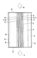
図3〜図6は、本発明の第1実施形態に係る量子ドットレーザの製造途中の断面図である。
以上により、本実施形態に係る量子ドットレーザの基本構造が完成したことになる。
上記した第1実施形態では量子ドットレーザを作製したが、本実施形態では量子ドット光増幅器を作成する。但し、その製造プロセスは、第1実施形態で説明した量子ドットレーザと同じなので、その説明は省略する。
前記半導体基板上に形成された下地層と、
前記下地層上に形成され、少なくともAs(砒素)とIII族元素とを含む混晶よりなる量子ドットと、
前記量子ドットの上に形成されたInpGa1-pAsqP1-q(0≦p, q≦1)よりなる第1バリア層と、
前記第1バリア層上に形成されたInrAlsGa1-r-sAs(0≦r, s≦1)よりなる第2バリア層と、
を有することを特徴とする光半導体装置。
前記下地層、前記量子ドット、及び前記第2バリア層の積層体の断面形状がメサ状であり、該積層体の両側に形成された埋め込み層と、前記埋め込み層の上に形成された電流ブロック層と、該電流ブロック層と前記積層体のそれぞれの上に形成された上部クラッド層とを有することを特徴とする付記1乃至付記4のいずれかに記載の光半導体装置。
第1の基板温度において、前記下地層の上に、少なくともAs(砒素)とIII族元素とを含む混晶よりなる量子ドットを形成する工程と、
第2の基板温度において、前記量子ドットの上に、InpGa1-pAsqP1-q(0≦p, q≦1)よりなる第1バリア層を形成する工程と、
前記第2の基板温度よりも高い第3の基板温度において、前記第1バリア層上に、InrAlsGa1-r-sAs(0≦r, s≦1)よりなる第2バリア層を形成する工程と、
を有することを特徴とする光半導体装置の製造方法。
Claims (1)
- 半導体基板の上にIn x Al y Ga 1-x-y As(0<x, y<1)よりなる下地層を形成する工程と、
第1の基板温度において、前記下地層の上に、少なくともInとAs(砒素)とIII族元素とを含む混晶よりなる量子ドットを形成する工程と、
第2の基板温度において、前記量子ドットの上に、InpGa1-pAsqP1-q(0<p, q<1)よりなる第1バリア層を形成する工程と、
前記第2の基板温度よりも高い第3の基板温度において、前記第1バリア層上に、InrAlsGa1-r-sAs(0<r, s<1)よりなる第2バリア層を形成する工程と、
を有し、
前記第1の基板温度と前記第2の基板温度は、450℃以上500℃以下であり、前記第3の基板温度は、600℃以上であることを特徴とする光半導体装置の製造方法。
Priority Applications (1)
| Application Number | Priority Date | Filing Date | Title |
|---|---|---|---|
| JP2005041669A JP4829508B2 (ja) | 2005-02-18 | 2005-02-18 | 光半導体装置の製造方法 |
Applications Claiming Priority (1)
| Application Number | Priority Date | Filing Date | Title |
|---|---|---|---|
| JP2005041669A JP4829508B2 (ja) | 2005-02-18 | 2005-02-18 | 光半導体装置の製造方法 |
Publications (2)
| Publication Number | Publication Date |
|---|---|
| JP2006229010A JP2006229010A (ja) | 2006-08-31 |
| JP4829508B2 true JP4829508B2 (ja) | 2011-12-07 |
Family
ID=36990096
Family Applications (1)
| Application Number | Title | Priority Date | Filing Date |
|---|---|---|---|
| JP2005041669A Expired - Lifetime JP4829508B2 (ja) | 2005-02-18 | 2005-02-18 | 光半導体装置の製造方法 |
Country Status (1)
| Country | Link |
|---|---|
| JP (1) | JP4829508B2 (ja) |
Families Citing this family (4)
| Publication number | Priority date | Publication date | Assignee | Title |
|---|---|---|---|---|
| JP2009141032A (ja) * | 2007-12-05 | 2009-06-25 | Fujitsu Ltd | 半導体装置の製造方法及び半導体装置 |
| WO2015198377A1 (ja) | 2014-06-23 | 2015-12-30 | 富士通株式会社 | 半導体レーザ光源及び半導体レーザ光源の製造方法 |
| JP6240738B2 (ja) * | 2016-11-09 | 2017-11-29 | アンリツ株式会社 | 半導体光増幅器 |
| JP2018107415A (ja) * | 2016-12-28 | 2018-07-05 | 株式会社Qdレーザ | 半導体レーザ |
Family Cites Families (11)
| Publication number | Priority date | Publication date | Assignee | Title |
|---|---|---|---|---|
| JP3534879B2 (ja) * | 1995-03-20 | 2004-06-07 | 富士通株式会社 | 3次元量子閉じ込めを利用した半導体装置 |
| JP3304903B2 (ja) * | 1998-12-21 | 2002-07-22 | 日本電気株式会社 | 半導体量子ドット素子とその製造方法 |
| JP4651759B2 (ja) * | 1998-12-25 | 2011-03-16 | 富士通株式会社 | 量子ドットを備えた素子 |
| JP2001085665A (ja) * | 1999-09-10 | 2001-03-30 | Fujitsu Ltd | 量子ドットを用いた半導体素子 |
| EP1354380A2 (en) * | 2000-10-06 | 2003-10-22 | Science & Technology Corporation UNM | Quantum dot lasers |
| JP4086465B2 (ja) * | 2000-12-27 | 2008-05-14 | 三菱化学株式会社 | 量子ドット構造体及びその形成方法、並びに該量子ドット構造体を有する半導体デバイス装置 |
| JP4117778B2 (ja) * | 2002-09-27 | 2008-07-16 | 日本電信電話株式会社 | 半導体光素子 |
| WO2004055900A1 (ja) * | 2002-12-16 | 2004-07-01 | Japan Science And Technology Agency | 不均一な量子ドットを有する半導体積層構造、それを用いた発光ダイオード、半導体レーザダイオード及び半導体光増幅器並びにそれらの製造方法 |
| JP4439193B2 (ja) * | 2003-03-20 | 2010-03-24 | 富士通株式会社 | 半導体光増幅器及び光増幅方法 |
| JP2004319743A (ja) * | 2003-04-16 | 2004-11-11 | Hitachi Ltd | 量子ドットを有する半導体構造体の製造方法、半導体構造体、及び半導体装置 |
| JP3771925B2 (ja) * | 2004-06-07 | 2006-05-10 | 日本電信電話株式会社 | 半導体量子ドット構造及びその製造方法 |
-
2005
- 2005-02-18 JP JP2005041669A patent/JP4829508B2/ja not_active Expired - Lifetime
Also Published As
| Publication number | Publication date |
|---|---|
| JP2006229010A (ja) | 2006-08-31 |
Similar Documents
| Publication | Publication Date | Title |
|---|---|---|
| US6351479B1 (en) | Semiconductor laser having effective output increasing function | |
| US8906721B2 (en) | Semiconductor light emitting device and method for manufacturing the same | |
| US8073029B2 (en) | Semiconductor optical device | |
| US7539385B2 (en) | Optical semiconductor device and fabrication process thereof | |
| JP4571635B2 (ja) | スーパールミネッセントダイオード | |
| JP2008053649A (ja) | 埋め込み型半導体レーザ | |
| US20080315182A1 (en) | Optical semiconductor device and method for manufacturing the same | |
| US9660420B2 (en) | Laser diode | |
| US7362788B2 (en) | Semiconductor laser and fabricating method thereof | |
| JP2008047684A (ja) | 半導体発光素子、その製造方法および半導体発光装置 | |
| JP2007201040A (ja) | 半導体発光素子 | |
| JP4797782B2 (ja) | 半導体光素子 | |
| JP4017196B2 (ja) | 分布帰還型半導体レーザ装置 | |
| US7957442B2 (en) | Semiconductor optical device | |
| JP2005286192A (ja) | 光集積素子 | |
| JP4829508B2 (ja) | 光半導体装置の製造方法 | |
| JP2007184491A (ja) | 分布帰還型半導体レーザ | |
| JP4886634B2 (ja) | 量子井戸構造、光閉じ込め型量子井戸構造、半導体レーザ、分布帰還型半導体レーザ、及び量子井戸構造の製造方法 | |
| JP2010010284A (ja) | 集積型光半導体装置の製造方法及び集積型光半導体装置 | |
| JP5026115B2 (ja) | 量子井戸構造、半導体レーザ、分光計測装置及び量子井戸構造の製造方法 | |
| JP5205901B2 (ja) | 半導体レーザ素子の作製方法および半導体レーザ素子 | |
| JP5617353B2 (ja) | 半導体素子 | |
| JP4617684B2 (ja) | 半導体レーザ素子 | |
| JPH0745902A (ja) | 半導体レーザおよびその製造方法 | |
| JP2006339311A (ja) | 半導体レーザ |
Legal Events
| Date | Code | Title | Description |
|---|---|---|---|
| A621 | Written request for application examination |
Free format text: JAPANESE INTERMEDIATE CODE: A621 Effective date: 20070803 |
|
| A977 | Report on retrieval |
Free format text: JAPANESE INTERMEDIATE CODE: A971007 Effective date: 20100713 |
|
| A131 | Notification of reasons for refusal |
Free format text: JAPANESE INTERMEDIATE CODE: A131 Effective date: 20100720 |
|
| A521 | Written amendment |
Free format text: JAPANESE INTERMEDIATE CODE: A523 Effective date: 20100913 |
|
| A131 | Notification of reasons for refusal |
Free format text: JAPANESE INTERMEDIATE CODE: A131 Effective date: 20110208 |
|
| A521 | Written amendment |
Free format text: JAPANESE INTERMEDIATE CODE: A523 Effective date: 20110408 |
|
| TRDD | Decision of grant or rejection written | ||
| A01 | Written decision to grant a patent or to grant a registration (utility model) |
Free format text: JAPANESE INTERMEDIATE CODE: A01 Effective date: 20110913 |
|
| A01 | Written decision to grant a patent or to grant a registration (utility model) |
Free format text: JAPANESE INTERMEDIATE CODE: A01 |
|
| A61 | First payment of annual fees (during grant procedure) |
Free format text: JAPANESE INTERMEDIATE CODE: A61 Effective date: 20110916 |
|
| FPAY | Renewal fee payment (event date is renewal date of database) |
Free format text: PAYMENT UNTIL: 20140922 Year of fee payment: 3 |
|
| R150 | Certificate of patent or registration of utility model |
Ref document number: 4829508 Country of ref document: JP Free format text: JAPANESE INTERMEDIATE CODE: R150 Free format text: JAPANESE INTERMEDIATE CODE: R150 |