JP4814862B2 - 液晶表示装置 - Google Patents
液晶表示装置 Download PDFInfo
- Publication number
- JP4814862B2 JP4814862B2 JP2007302882A JP2007302882A JP4814862B2 JP 4814862 B2 JP4814862 B2 JP 4814862B2 JP 2007302882 A JP2007302882 A JP 2007302882A JP 2007302882 A JP2007302882 A JP 2007302882A JP 4814862 B2 JP4814862 B2 JP 4814862B2
- Authority
- JP
- Japan
- Prior art keywords
- electrode
- transmissive
- reflective
- liquid crystal
- reflective electrode
- Prior art date
- Legal status (The legal status is an assumption and is not a legal conclusion. Google has not performed a legal analysis and makes no representation as to the accuracy of the status listed.)
- Expired - Lifetime
Links
- 239000004973 liquid crystal related substance Substances 0.000 title claims description 25
- 239000000463 material Substances 0.000 claims description 29
- 239000000758 substrate Substances 0.000 claims description 28
- 239000010408 film Substances 0.000 description 48
- 239000010410 layer Substances 0.000 description 28
- 239000007772 electrode material Substances 0.000 description 23
- 239000004065 semiconductor Substances 0.000 description 23
- 239000011229 interlayer Substances 0.000 description 20
- 238000000206 photolithography Methods 0.000 description 18
- 238000000034 method Methods 0.000 description 17
- 239000011159 matrix material Substances 0.000 description 13
- 229910052782 aluminium Inorganic materials 0.000 description 8
- 239000010409 thin film Substances 0.000 description 8
- 229910052750 molybdenum Inorganic materials 0.000 description 7
- 229910052719 titanium Inorganic materials 0.000 description 7
- 229910052721 tungsten Inorganic materials 0.000 description 7
- 229910021417 amorphous silicon Inorganic materials 0.000 description 6
- 229910052802 copper Inorganic materials 0.000 description 6
- 239000011347 resin Substances 0.000 description 6
- 229920005989 resin Polymers 0.000 description 6
- 229910052751 metal Inorganic materials 0.000 description 5
- 239000002184 metal Substances 0.000 description 5
- 238000009751 slip forming Methods 0.000 description 5
- VEXZGXHMUGYJMC-UHFFFAOYSA-N Hydrochloric acid Chemical compound Cl VEXZGXHMUGYJMC-UHFFFAOYSA-N 0.000 description 4
- 229910052804 chromium Inorganic materials 0.000 description 4
- 239000004020 conductor Substances 0.000 description 4
- 238000005530 etching Methods 0.000 description 4
- 229910052715 tantalum Inorganic materials 0.000 description 4
- 229910004205 SiNX Inorganic materials 0.000 description 3
- 238000005229 chemical vapour deposition Methods 0.000 description 3
- 230000007547 defect Effects 0.000 description 3
- 239000011521 glass Substances 0.000 description 3
- 229910003437 indium oxide Inorganic materials 0.000 description 3
- PJXISJQVUVHSOJ-UHFFFAOYSA-N indium(iii) oxide Chemical compound [O-2].[O-2].[O-2].[In+3].[In+3] PJXISJQVUVHSOJ-UHFFFAOYSA-N 0.000 description 3
- LXFUCSMCVAEMCD-UHFFFAOYSA-N acetic acid;nitric acid;phosphoric acid Chemical compound CC(O)=O.O[N+]([O-])=O.OP(O)(O)=O LXFUCSMCVAEMCD-UHFFFAOYSA-N 0.000 description 2
- 239000002253 acid Substances 0.000 description 2
- 238000004519 manufacturing process Methods 0.000 description 2
- 230000015572 biosynthetic process Effects 0.000 description 1
- 238000010586 diagram Methods 0.000 description 1
- 239000011810 insulating material Substances 0.000 description 1
- 238000009413 insulation Methods 0.000 description 1
- 150000002739 metals Chemical class 0.000 description 1
- 229910052759 nickel Inorganic materials 0.000 description 1
- 229910052697 platinum Inorganic materials 0.000 description 1
- 239000011241 protective layer Substances 0.000 description 1
- 229910052709 silver Inorganic materials 0.000 description 1
Images


Landscapes
- Liquid Crystal (AREA)
Description
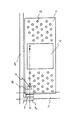
図1に、透過反射両用型液晶表示装置のアクティブマトリクス基板の1絵素の構成を示す。図2に図1のA−A断面を示す。
図3に実施形態2のアクティブマトリクス基板を示す。実施形態1と同一構成には同一の符号を付している。
図4に実施形態3のアクティブマトリクス基板を示す。実施形態1と同一構成には同一の符号を付している。
2 ゲート電極
3 ゲート配線
4 ゲート絶縁膜
5 半導体層
6a 半導体コンタクト層(ソース電極側)
6b 半導体コンタクト層(ドレイン電極側)
7 TFT部
8 透過電極
9a ソース配線
9b ソース電極
9c ドレイン電極
10 層間絶縁膜
11 反射電極
12 コンタクト部
13 透過領域
14 反射電極凹凸部
15 透過電極材料
16 反射電極材料
Claims (1)
- 絶縁性基板に形成されたスイッチング素子と、前記スイッチング素子と電気的に接続された絵素電極とを備えた液晶表示装置において、
前記絵素電極は透過材料と反射材料とで形成され、前記絵素電極が形成された領域は透過表示領域と反射表示領域とを有し、前記透過表示領域では前記反射材料を形成することなく前記透過材料によって前記絵素電極が形成され、前記透過表示領域と前記反射表示領域との境界領域では前記反射材料が前記透過材料の上層に積層され、前記反射表示領域では前記透過材料を形成することなく前記反射材料によって前記絵素電極が形成されていることを特徴とする液晶表示装置。
Priority Applications (1)
| Application Number | Priority Date | Filing Date | Title |
|---|---|---|---|
| JP2007302882A JP4814862B2 (ja) | 2007-11-22 | 2007-11-22 | 液晶表示装置 |
Applications Claiming Priority (1)
| Application Number | Priority Date | Filing Date | Title |
|---|---|---|---|
| JP2007302882A JP4814862B2 (ja) | 2007-11-22 | 2007-11-22 | 液晶表示装置 |
Related Parent Applications (1)
| Application Number | Title | Priority Date | Filing Date |
|---|---|---|---|
| JP2002297383A Division JP4084630B2 (ja) | 2002-10-10 | 2002-10-10 | 液晶表示装置 |
Publications (2)
| Publication Number | Publication Date |
|---|---|
| JP2008102542A JP2008102542A (ja) | 2008-05-01 |
| JP4814862B2 true JP4814862B2 (ja) | 2011-11-16 |
Family
ID=39436852
Family Applications (1)
| Application Number | Title | Priority Date | Filing Date |
|---|---|---|---|
| JP2007302882A Expired - Lifetime JP4814862B2 (ja) | 2007-11-22 | 2007-11-22 | 液晶表示装置 |
Country Status (1)
| Country | Link |
|---|---|
| JP (1) | JP4814862B2 (ja) |
Family Cites Families (3)
| Publication number | Priority date | Publication date | Assignee | Title |
|---|---|---|---|---|
| JP2793076B2 (ja) * | 1992-05-20 | 1998-09-03 | シャープ株式会社 | 反射型液晶表示装置およびその製造方法 |
| JPH07218923A (ja) * | 1994-01-28 | 1995-08-18 | Toppan Printing Co Ltd | 反射型液晶表示装置 |
| JPH07318929A (ja) * | 1994-05-30 | 1995-12-08 | Casio Comput Co Ltd | 液晶表示装置 |
-
2007
- 2007-11-22 JP JP2007302882A patent/JP4814862B2/ja not_active Expired - Lifetime
Also Published As
| Publication number | Publication date |
|---|---|
| JP2008102542A (ja) | 2008-05-01 |
Similar Documents
| Publication | Publication Date | Title |
|---|---|---|
| JP3410656B2 (ja) | 液晶表示装置及びその製造方法 | |
| JP4543385B2 (ja) | 液晶表示装置の製造方法 | |
| JP4191642B2 (ja) | 半透過型液晶表示装置およびその製造方法 | |
| US7833813B2 (en) | Thin film transistor array panel and method of manufacturing the same | |
| JP2008010440A (ja) | アクティブマトリクス型tftアレイ基板およびその製造方法 | |
| CN100517734C (zh) | Tft阵列衬底的制造方法 | |
| JP4083752B2 (ja) | アクティブマトリクス基板及びその製造方法 | |
| US8520183B2 (en) | Display substrate, liquid crystal display including the display substrate, and method of manufacturing the display substrate | |
| JP4802462B2 (ja) | 薄膜トランジスタアレイ基板の製造方法 | |
| KR19990083238A (ko) | 액정표시장치, 매트릭스 어레이기판 및 그 제조방법 | |
| CN103091915B (zh) | 布线构造、包括它的薄膜晶体管阵列基板及显示装置 | |
| JP6103854B2 (ja) | 薄膜トランジスタ基板 | |
| JP6501514B2 (ja) | 薄膜トランジスタ基板およびその製造方法 | |
| KR20110114906A (ko) | 표시기판 및 그 제조방법 | |
| US20090117333A1 (en) | Method of manufacturing display device and display device therefrom | |
| US6559920B1 (en) | Liquid crystal display device and method of manufacturing the same | |
| KR20060125066A (ko) | 개구율이 향상된 어레이 기판 및 이의 제조방법 | |
| KR20090078527A (ko) | 표시 기판 | |
| JP4084630B2 (ja) | 液晶表示装置 | |
| JP4814862B2 (ja) | 液晶表示装置 | |
| JP4799926B2 (ja) | 半透過型tftアレイ基板、および半透過型液晶表示装置 | |
| JP6180200B2 (ja) | アクティブマトリクス基板およびその製造方法 | |
| JP4227055B2 (ja) | 液晶表示装置の製造方法 | |
| JP5032188B2 (ja) | 液晶表示装置及びその製造方法 | |
| CN107403805A (zh) | 薄膜晶体管阵列面板及其制造方法 |
Legal Events
| Date | Code | Title | Description |
|---|---|---|---|
| RD01 | Notification of change of attorney |
Free format text: JAPANESE INTERMEDIATE CODE: A7421 Effective date: 20100513 |
|
| A131 | Notification of reasons for refusal |
Free format text: JAPANESE INTERMEDIATE CODE: A131 Effective date: 20100803 |
|
| A131 | Notification of reasons for refusal |
Free format text: JAPANESE INTERMEDIATE CODE: A131 Effective date: 20110315 |
|
| A521 | Written amendment |
Free format text: JAPANESE INTERMEDIATE CODE: A523 Effective date: 20110322 |
|
| TRDD | Decision of grant or rejection written | ||
| A01 | Written decision to grant a patent or to grant a registration (utility model) |
Free format text: JAPANESE INTERMEDIATE CODE: A01 Effective date: 20110809 |
|
| A01 | Written decision to grant a patent or to grant a registration (utility model) |
Free format text: JAPANESE INTERMEDIATE CODE: A01 |
|
| A61 | First payment of annual fees (during grant procedure) |
Free format text: JAPANESE INTERMEDIATE CODE: A61 Effective date: 20110826 |
|
| R150 | Certificate of patent or registration of utility model |
Free format text: JAPANESE INTERMEDIATE CODE: R150 |
|
| FPAY | Renewal fee payment (event date is renewal date of database) |
Free format text: PAYMENT UNTIL: 20140902 Year of fee payment: 3 |
|
| EXPY | Cancellation because of completion of term |