JP4787273B2 - Secure memory card with life cycle phase - Google Patents
Secure memory card with life cycle phase Download PDFInfo
- Publication number
- JP4787273B2 JP4787273B2 JP2007554249A JP2007554249A JP4787273B2 JP 4787273 B2 JP4787273 B2 JP 4787273B2 JP 2007554249 A JP2007554249 A JP 2007554249A JP 2007554249 A JP2007554249 A JP 2007554249A JP 4787273 B2 JP4787273 B2 JP 4787273B2
- Authority
- JP
- Japan
- Prior art keywords
- memory card
- state
- test
- key
- card
- Prior art date
- Legal status (The legal status is an assumption and is not a legal conclusion. Google has not performed a legal analysis and makes no representation as to the accuracy of the status listed.)
- Expired - Fee Related
Links
Images


Classifications
-
- G—PHYSICS
- G06—COMPUTING OR CALCULATING; COUNTING
- G06F—ELECTRIC DIGITAL DATA PROCESSING
- G06F11/00—Error detection; Error correction; Monitoring
- G06F11/22—Detection or location of defective computer hardware by testing during standby operation or during idle time, e.g. start-up testing
- G06F11/2273—Test methods
-
- G—PHYSICS
- G06—COMPUTING OR CALCULATING; COUNTING
- G06K—GRAPHICAL DATA READING; PRESENTATION OF DATA; RECORD CARRIERS; HANDLING RECORD CARRIERS
- G06K19/00—Record carriers for use with machines and with at least a part designed to carry digital markings
- G06K19/06—Record carriers for use with machines and with at least a part designed to carry digital markings characterised by the kind of the digital marking, e.g. shape, nature, code
- G06K19/067—Record carriers with conductive marks, printed circuits or semiconductor circuit elements, e.g. credit or identity cards also with resonating or responding marks without active components
- G06K19/07—Record carriers with conductive marks, printed circuits or semiconductor circuit elements, e.g. credit or identity cards also with resonating or responding marks without active components with integrated circuit chips
-
- G—PHYSICS
- G06—COMPUTING OR CALCULATING; COUNTING
- G06F—ELECTRIC DIGITAL DATA PROCESSING
- G06F1/00—Details not covered by groups G06F3/00 - G06F13/00 and G06F21/00
-
- G—PHYSICS
- G06—COMPUTING OR CALCULATING; COUNTING
- G06F—ELECTRIC DIGITAL DATA PROCESSING
- G06F12/00—Accessing, addressing or allocating within memory systems or architectures
- G06F12/14—Protection against unauthorised use of memory or access to memory
Landscapes
- Engineering & Computer Science (AREA)
- Theoretical Computer Science (AREA)
- Physics & Mathematics (AREA)
- General Physics & Mathematics (AREA)
- General Engineering & Computer Science (AREA)
- Computer Hardware Design (AREA)
- Microelectronics & Electronic Packaging (AREA)
- Computer Security & Cryptography (AREA)
- Quality & Reliability (AREA)
- Storage Device Security (AREA)
- Credit Cards Or The Like (AREA)
Description
本発明は、一般に、メモリカードおよび暗号化に関し、特に、カードのテスト機構によるセキュアデータおよび鍵へのアクセス排除に関する。 The present invention relates generally to memory cards and encryption, and more particularly to exclusion of access to secure data and keys by a card testing mechanism.
開発からかなりの時が経過した、スマートカードと一般に呼ばれているインテリジェントメモリカードは、身分証明や支払いの形態で市場に受け入れられている。スマートカードは、ユーザの識別データの格納および取引関連データの格納用の少量のメモリを含む。また、スマートカードは、チップと呼ばれることも多く、日本では、国の身分証明書などのさまざまな形態や、クレジットカードやデビットカードのタイプとしてさまざまな場所で採用されている。なりすまし犯罪やその他の金銭上の詐欺を防止するために、カードおよびカードを利用するシステムに、さまざまなチップデザインおよび暗号化方式が採用されてきた。 A considerable amount of time has passed since development, and intelligent memory cards, commonly referred to as smart cards, are accepted by the market in the form of identification and payment. The smart card includes a small amount of memory for storing user identification data and transaction related data. Smart cards are often called chips. In Japan, smart cards are used in various places such as national identity cards and credit cards and debit cards. Various chip designs and encryption schemes have been employed in cards and card-based systems to prevent impersonation crimes and other financial fraud.
任意のタイプのセキュアメモリカードの設計と製造には、2つの競合する利益が存在する。1つの利益は、カードのセキュリティを最大限に高めることであり、もう1つの利益は、カードの信頼性を最大限に高めることである。カードの信頼性を最大限に高めるには、工場からの出荷前に、場合によっては、工場からの出荷後であっても、故障解析を行うために、さまざまな製造段階でカードのソフトウェアおよびハードウェアをテストできることが重要である。カードのハードウェアとソフトウェアの両方をテストするために、チップ上のテストまたはコンタクトパッドに信号を入出力させてテストを行ってもよい。これらのテストルーチンおよびテストパッドは、品質制御を確保する必要があるが、セキュアデータ、アルゴリズム、およびカードの鍵にとって、潜在的な弱点、いわゆる「抜け穴」となる。このように、信頼性の最大化とセキュリティの最大化(に必要なテスト)の間には、ある程度の妥協が常に存在する。テスト完了後、この「抜け穴」を閉じるためのさまざまなアプローチがこれまで提案されてきた。しかし、さまざまな理由から、これまでの解決策にはそれぞれ、商業的および技術的欠点がある。 There are two competing benefits in the design and manufacture of any type of secure memory card. One benefit is to maximize card security, and another benefit is to maximize card reliability. To maximize the reliability of the card, the card software and hardware at various stages of production can be analyzed before failure from the factory, and in some cases even after shipment from the factory, for failure analysis. It is important to be able to test the wear. In order to test both the hardware and software of the card, the test may be performed by inputting / outputting signals to / from a test on a chip or a contact pad. While these test routines and test pads need to ensure quality control, they are a potential weakness for secure data, algorithms, and card keys, so-called “loopholes”. Thus, there is always some degree of compromise between maximizing reliability and maximizing security (the tests required for). Various approaches have been proposed to close this “loophole” after testing is complete. However, for various reasons, each of the previous solutions has commercial and technical drawbacks.
前述したスマートカードの作製に採用されると考えられる1つのアプローチにおいて、ウェハからメモリダイを個片化する前にカードのダイがテストされる。特定のダイ用のテストパッドは、ウェハの隣接するダイの上に設けられ、個片化プロセスは、テスト後に隣接するダイのすべての回路からテストパッドを切断する。したがって、個片化されたダイの上に存在するあらゆるテストパッドが完全に隔離され、最終メモリカードのセキュアデータへの潜在的な抜け穴として閉じられる。しかし、テストパッドを完全に除去することは、常に実用的なことでも、望ましいことでもない。例えば、使用可能なテストパッドがないと、ある量のハードウェアベースのメモリテストを引き続き行えなくなり、これにより、例えば、潜在的な故障解析方法を制限してしまう。 In one approach that may be employed in the smart card fabrication described above, the card die is tested before the memory die is singulated from the wafer. A test pad for a particular die is provided on the adjacent die of the wafer, and the singulation process cuts the test pad from all circuitry on the adjacent die after testing. Thus, any test pads present on the singulated die are completely isolated and closed as a potential loophole to the secure data on the final memory card. However, complete removal of the test pad is not always practical or desirable. For example, without a usable test pad, a certain amount of hardware-based memory testing cannot continue, which limits, for example, potential failure analysis methods.
このアプローチは、典型的に、身分証明および取引データの保持に必要なメモリを少量しかもたないスマートカードには好ましいこともあるが、写真や音楽などの多数の大きなファイルを格納するのに使用する大容量メモリカードに採用された比較的大量のメモリおよび複雑なセキュリティルーチンをテストするには不十分である。これらの大容量メモリカードのいくつかの例は、コンパクトフラッシュカード、MMCカード、およびSDカードである。デジタルコンテンツの普及と、それに関連する著作権問題により、セキュリティの重要性が高まると同時に、カードのテストおよび信頼性が最も重要であることに変わりはない。セキュアな大容量メモリカードを製造、テスト、および動作させるより包括的かつ柔軟性のあるシステムが必要とされ、以下に説明する本発明によって提供される。 This approach is typically used to store large numbers of large files such as photos and music, although it may be preferable for smart cards that have only a small amount of memory required to hold identification and transaction data It is insufficient to test the relatively large amount of memory and complex security routines employed in high capacity memory cards. Some examples of these large capacity memory cards are compact flash cards, MMC cards, and SD cards. With the proliferation of digital content and the associated copyright issues, the importance of security is increasing, while card testing and reliability remain the most important. There is a need for a more comprehensive and flexible system for manufacturing, testing, and operating secure mass memory cards and is provided by the present invention described below.
別の重要な態様はコストである。不揮発性メモリ、論理、揮発性メモリなどのいくつかの異なる技術が、単一の集積回路ダイ(チップ)上に作製されうる。しかし、1つのダイでさまざまな技術を混在させると、生産コストが著しく増大する。コストが主要な原動力である競合的な環境において、1つのダイに与えられる、異なる技術の数を制限することが非常に望ましい。しかし、複数のダイを使用するということは、つまり、最終製品の1つのダイから別のダイへ機密情報を渡す必要があるということにもなる。これは、適切な予防策を取り入れていなければ、ハッカーが利用できる別の潜在的な弱点となる。 Another important aspect is cost. Several different technologies such as non-volatile memory, logic, volatile memory, etc. can be fabricated on a single integrated circuit die (chip). However, when various technologies are mixed in one die, the production cost is remarkably increased. In competitive environments where cost is a major driving force, it is highly desirable to limit the number of different technologies that can be given to a die. However, using multiple dies also means that confidential information needs to be passed from one die to another in the final product. This is another potential weakness that hackers can take advantage of without proper precautions.
特に、不揮発性メモリビットは、同じダイ内で論理と混在させるには高価である。スマートカードは、スマートカードを実行する論理と同じダイでデータ記憶を目的として不揮発性メモリを採用し、これは、セキュリティを最大限に高める1つの方法である。しかし、今日、本発明から利益を享受するメモリカードは、非常に大きな、音楽、写真、映像、および他のユーザファイルを格納しなければならない。このように、大量の情報(2005年時点で数ギガバイト程度であるが、さらに増大)を格納可能な単一の集積回路ダイメモリカードの製造には法外なコストがかかり、複数のダイを採用するセキュアシステムの開発が必要である。特に、コントローラダイから分離され、アセンブリの前後に十分にテスト可能であるが、テスト機構を経由した攻撃を受けにくい1つ以上のディスクリート(コスト効率の良い)フラッシュメモリダイを利用したセキュアシステム(暗号化および復号化を採用)の作製が非常に望ましい。
コントローラの機能性と、今日のデジタルデバイスが要求する大容量記憶とを兼ね備えた単一チップを利用することは、過度にコストがかかるとともに、拡張性の点でも問題があるため、代替のシステムが開発されてきた。単一チップの解決策の場合、テスト機構、暗号化鍵、および暗号化されたコンテンツへアクセスしにくくする特有のチップデザインでセキュリティを確保できる。しかし、コンテンツが別個のメモリチップから、暗号化が生じるコントローラチップに渡される複数チップデザインの場合、暗号化鍵と暗号化されたコンテンツへのアクセス保護に特に注意を払わなければならない。さらに、組立て済みのシステムをテストできるように最終アセンブリに(好ましくは)依然としてテストパッドを備えたシステムでは、暗号化鍵およびコンテンツへの不正アクセスへの抜け穴となってしまいかねないソフトウェアおよびハードウェアの任意の機構に特に注意を払わなければならない。 Using a single chip that combines the functionality of a controller with the mass storage required by today's digital devices is overly costly and has scalability issues, so alternative systems Has been developed. In the case of a single chip solution, security can be ensured with a unique chip design that makes it difficult to access the test mechanism, encryption key, and encrypted content. However, in the case of a multi-chip design where content is passed from a separate memory chip to the controller chip where encryption occurs, particular attention must be paid to the encryption key and access protection to the encrypted content. In addition, a system that still has a test pad (preferably) in the final assembly so that the assembled system can be tested can be used as software and hardware that could be a loophole for unauthorized access to encryption keys and content. Special attention must be paid to any mechanism.
本発明は、カードの寿命の間に入り通過する多数のライフサイクルフェーズを有する。フェーズに応じて、カードの論理は、暗号化エンジンを有効または無効にし、(ウェハの個片化およびカードの組み立ての前後での)ハードウェアおよびソフトウェアテスト機構へのアクセスを制御し、鍵生成を制御する。これらのフェーズは、(テストパッドを除去したスマートカードとは異なり)カードのハードウェアとソフトウェアの両方を製造の前後で徹底的にテストできるようになるだけでなく、カードがセキュアフェーズにあるとき、すなわち、カードがユーザに出荷されているときのカードの状態である動作フェーズにあるとき、暗号化された鍵、ひいては、暗号化されたコンテンツへ事実上アクセスできなくする。したがって、本発明により、十分にテスト可能であるが、カード内の保護データへの不正アクセスにも強いメモリカードが提供される。 The present invention has a number of life cycle phases that pass through the lifetime of the card. Depending on the phase, the card logic enables or disables the encryption engine, controls access to hardware and software test mechanisms (before and after wafer singulation and card assembly), and generates keys. Control. These phases (unlike smart cards with the test pad removed) will not only allow thorough testing of both the card hardware and software before and after production, but also when the card is in the secure phase, That is, when in the operational phase, which is the state of the card when it is shipped to the user, the encrypted key and thus the encrypted content is virtually inaccessible. Therefore, the present invention provides a memory card that can be fully tested but is resistant to unauthorized access to protected data in the card.
さらに、セキュアな大容量メモリカードを製造、テスト、および動作させるより包括的かつ柔軟性のあるシステムが必要とされ、以下に説明する本発明により提供される。 Furthermore, there is a need for a more comprehensive and flexible system for manufacturing, testing, and operating secure mass memory cards and is provided by the present invention described below.
本発明のさらなる態様、利点、および特徴は、添付の図面と関連して参照される本発明の例示的な実施例の以下の説明に含まれ、図面において、同じ特徴を説明するために同様の参照番号を使用している。本願明細書において参照したすべての特許、特許出願、論文、および他の刊行物は、あらゆる目的のためにその全体が本願明細書において参照により援用されている。 Additional aspects, advantages, and features of the present invention are included in the following description of exemplary embodiments of the invention, referenced in conjunction with the accompanying drawings, in which like features are used to describe the same features. A reference number is used. All patents, patent applications, articles, and other publications referenced herein are hereby incorporated by reference in their entirety for all purposes.
(メモリシステム構造)
図1Aのブロック図に、本発明のさまざまな態様が実施されてもよい例示的なメモリシステムを示す。図1Aに示されているように、メモリシステム10は、中央演算処理装置(CPU)またはコントローラ12と、バッファ管理ユニット(BMU)14と、ホストインターフェイスモジュール(HIM)16と、フラッシュインターフェイスモジュール(FIM)18と、フラッシュメモリ20と、周辺アクセスモジュール22とを含む。メモリシステム10は、ホストインターフェイスバス26およびポート26aを介してホストデバイス24と通信する。NAND形のものであってもよいフラッシュメモリ20は、ホストデバイス24にデータ記憶装置を提供する。また、CPU12のソフトウェアコードは、フラッシュメモリ20に格納される。FIM18は、フラッシュインターフェイスバス28を介して、場合によっては、フラッシュメモリ20が取り外し可能な構成要素であれば、図に示されていないが、ポートを介してフラッシュメモリ20に接続される。HIM16は、デジタルカメラ、パーソナルコンピュータ、個人用携帯情報端末(PDA)およびMP−3プレイヤ、携帯電話、または他のデジタルデバイスのようなホストシステムとの接続に適している。周辺アクセスモジュール22は、CPU12との通信用のFIM、HIM、およびBMUなどの適切なコントローラモジュールを選択する。1つの実施形態において、点線で四角に囲んだシステム10の構成要素はすべて、メモリカードなどの単一のユニットに封入されてもよく、好ましくは、カードに封入されてもよい。
(Memory system structure)
The block diagram of FIG. 1A illustrates an exemplary memory system in which various aspects of the invention may be implemented. As shown in FIG. 1A, the
バッファ管理ユニット14は、ホストダイレクトメモリアクセスユニット(HDMA)32と、フラッシュダイレクトメモリアクセスユニット(FDMA)34と、アービタ36と、CPUバスアービタ35と、レジスタ33と、バッファランダムアクセスメモリ(BRAM)38と、暗号化エンジン40とも呼ばれる暗号エンジン40とを備える。アービタ36は、1つのみのマスタまたはイニシエータ(HDMA32、FDMA34、またはCPU12でありうる)が、常に活性であり、スレーブまたはターゲットがBRAM38になるような共有バスアービタである。アービタは、BRAM38に適切なイニシエータのリクエストを通す責任を有する。HDMA32およびFDMA34は、HIM16と、FIM18と、BRAM38またはRAM11との間で伝送されるデータに責任を有する。CPUバスアービタ35は、暗号エンジン40およびフラッシュDMA34から、システムバス15を経由して、RAM11へ直接データを転送でき、これは、例えば、暗号エンジンを経由しないことが望ましい場合などの状況下で使用される。HDMA32およびFDMA34の動作は、従来のものであり、本願明細書で詳細に説明しない。BRAM38は、ホストデバイス24とフラッシュメモリ20との間を通るデータを格納するために使用される。HDMA32およびFDMA34は、HIM16/FIM18とBRAM38またはCPU RAM12aとの間でデータを転送したり、セクタの完了を示したりする責任を有する。
The buffer management unit 14 includes a host direct memory access unit (HDMA) 32, a flash direct memory access unit (FDMA) 34, an
フラッシュメモリ20からのデータがホストデバイス24によって読み出されるとき、メモリ20の暗号化データが、バス28、FIM18、FDMA34、および暗号エンジン40を通って取り出され、暗号化データは復号化され、BRAM38に格納される。次いで、復号化されたデータは、BRAM38から、HDMA32、HIM16、バス26を通って、ホストデバイス24に送信される。BRAM38から取り出されたデータは、ホストデバイス24に送信されたデータが再度暗号化されるようにHDMA32に渡される前に暗号エンジン40を用いて再度暗号化されてもよいが、メモリ20に格納されたデータが暗号化されたものと比較して異なった鍵および/またはアルゴリズムを用いて再度暗号化されてもよい。他の形態において、データが不正アクセスに脆弱になる可能性のある前述したプロセスにおいて、BRAM38に復号化データを格納するのではなく、メモリ20からのデータは、BRAM38に送信される前に暗号エンジン40によって再度復号化および暗号化されてもよい。次いで、BRAM38の暗号化データは、前述したように、ホストデバイス24に送信される。これは、読み出しプロセス中のデータストリームを示す。
When data from the flash memory 20 is read by the
データがホストデバイス24によってメモリ20に書き込まれると、データストリームの方向が反転する。例えば、暗号化されていないデータが、ホストデバイスによって、バス26、HIM16、HDMA32を通って、暗号エンジン40に送信されれば、このようなデータは、BRAM38に格納される前にエンジン40によって暗号化されてもよい。他の形態において、暗号化されていないデータは、BRAM38に格納されてもよい。次いで、データは、メモリ20へ進む途中でFDMA34に送信される前に暗号化される。
When data is written to the memory 20 by the
(ライフサイクルフェーズ)
例えば、前述したもののようなメモリカードに実装される場合に特に有用であるセキュリティシステムまたはセキュアオペレーティングシステムには、異なるフェーズまたは状態がある。これらのフェーズは、1つのフェーズから次へと進んだ後、前のフェーズには再度入ることができないように、連続的に入ることが好ましい。したがって、これらのフェーズは、ライフサイクルフェーズと考えることができる。
(Life cycle phase)
For example, security systems or secure operating systems that are particularly useful when implemented on a memory card such as those described above have different phases or states. These phases are preferably entered continuously after proceeding from one phase to the next so that the previous phase cannot be entered again. Therefore, these phases can be considered life cycle phases.
フェーズについて詳細に説明する前に、別のシステムレベル図について簡単に説明する。図1Bは、システム10の別の実施形態を示す。この図には、簡潔かつ明確に示すために、システム10のある一定の構成要素しか示されていない。メモリシステム10は、ハードウェアテスト入出力(I/O)54とも呼ばれるテストパッドを備える。ハードウェアバス(HWバス)56は、テストパッド54に接続されることが好ましい。これらのテストパッドおよびHWバス56は、システム10のさまざまなハードウェアおよび回路(図示せず)に接続され、システム10のハードウェアおよび回路をテストするために使用される。JTAGバス62は、システムバス15(図1Aに示されている)に接続され、コントローラファームウェアを取り替え、システム10の外側からハードウェアブロックを駆動するために使用できる。これは、レジスタの読み出し/書き込み動作を要求するハードウェアテスト用に使用される。JTAGバス62は、RAMおよびROMにアクセスできるため、システム10のファームウェアをテストするためにも使用される。診断コマンドをシステム10に送信するために、ホストバス26が利用され、システムのファームウェアをテストするためにも使用される。
Before describing the phases in detail, another system level diagram is briefly described. FIG. 1B illustrates another embodiment of the
また、暗号化エンジン40のNVM50が示されている。NVM50内に格納されているものは、ライフサイクル状態77および秘密鍵99(の値)である。NVMテストポート58は、暗号化エンジン40内のNVMをテストするために使用される。
Also shown is the
状態インジケータヒューズ66は、製品が、NVMコンテンツに依存するのではなく、(以下に説明する)NVM状態110にあることを表示するために使用される。その理由は、作製中にNVMに格納された初期値の信頼性を保証できないことが挙げられる。したがって、ヒューズなどの別のより信頼性の高いインジケータが使用される。このシステムは、ヒューズが設定されていれば、状態110にあることを決定する。システム10がリセットされれば、状態を決定するために、NVMライフサイクル状態77を見ることになる。
The
図2Aは、さまざまな状態と、状態間の遷移の順序を示す。各状態は、図2Bにも再現している以下の表から分かるように、カードの製造の前後のカード(またはカードが実現されるシステム)のさまざまな挙動および能力を既定する。
状態は、暗号化エンジンの不揮発性メモリ内に、32ビット値として格納されることが好ましい。状態120〜170を表すために使用される大量の可能な(≒109 )の組み合わせから、予め割り当てられた値が6つある。他のすべての値は、状態110を表す。これは、作製、組み立て、テスト、および出荷中のさまざまな処理動作が、メモリに格納された任意の値を変更してしまう可能性があるため、作製中に既定値を確実に格納し、その後に取り出すことが確保できないためである。
The state is preferably stored as a 32-bit value in the non-volatile memory of the encryption engine. From the large number of possible (≈10 9 ) combinations used to represent states 120-170, there are six pre-assigned values. All other values represent
また、鍵の値は、暗号化エンジンの不揮発性メモリに、128ビットフィールドとして格納されることが好ましい。鍵の値は、通常、シードアルゴリズムによって、ランダムに生成される。鍵の再生成は、鍵の値を変更してしまう可能性が高いが、(擬似)乱数発生器が、実際、連続して同じ値を発生してしまうこともあるため、これは保証できない。しかし、再生成中に鍵の値が変更されないこともあるということが十分に理解されたものであっても、鍵の変更という用語は、本願明細書において、鍵の再生成という用語と交換可能に使用される。言うまでもなく、情報を暗号化するために使用する鍵の値は重要なものである。同じ鍵の値は、暗号化と復号化の両方で使用されなければならない。このように、鍵の値が、システムの起動時ごとに再生成されれば、起動前に暗号化されたデータは、新しい鍵では復号化できないため、事実上、価値のないものになる。データは、カードのメモリに物理的にまだ存在はするが、ロックを解除するための適切な鍵の値がなければ役に立たない。このように、ハッカーが、どうにかしてカードをセキュア状態150ではない状態に戻そうとしても、価値のある情報を得ることはできない。状態110および160において、起動時ごとに新しい鍵が生成され、状態150において情報をすでに格納するために使用した鍵は、その情報を復号化するために利用することはできない。状態170および110において、暗号化エンジンは、鍵の値に関係なく、単に利用不能である。
The key value is preferably stored as a 128-bit field in the non-volatile memory of the encryption engine. The key value is usually randomly generated by a seed algorithm. Key regeneration is likely to change the key value, but this cannot be guaranteed because the (pseudo) random number generator may actually generate the same value continuously. However, even though it is well understood that the value of a key may not change during regeneration, the term key change is interchangeable with the term key regeneration herein. Used for. Needless to say, the value of the key used to encrypt the information is important. The same key value must be used for both encryption and decryption. In this way, if the key value is regenerated every time the system is activated, the data encrypted before the activation cannot be decrypted with the new key, and thus becomes virtually worthless. The data is still physically present in the card's memory but is useless without the proper key value to unlock it. Thus, even if a hacker manages to return the card to a state other than the
別のセキュリティ手段は、ファームウェアおよびハードウェアのテスト機構の利用を制限することを含む。このシステムは、この機構を有効化または無効化する論理を備える。前述したホストバスは、カードのファームウェアをテストするために使用される機構の1つである。ホストは、ファームウェアをテストするために、ホストバス上で診断コマンドを発行できる。また、ハードウェアは、これらのコマンドの実行時にテストされてもよい。また、ハードウェアは、JTAGポートとともにハードウェアバス上で直接テストされ、これにより、システムのさまざまなメモリへの直接アクセスが得られる。状態140および150において、NVMテスト機構、HWテスト機構、およびFWテスト機構がすべて無効化されていることに留意されたい。
Another security measure includes limiting the use of firmware and hardware test mechanisms. The system includes logic to enable or disable this mechanism. The host bus described above is one of the mechanisms used to test the card firmware. The host can issue diagnostic commands on the host bus to test the firmware. The hardware may also be tested when these commands are executed. The hardware is also tested directly on the hardware bus along with the JTAG port, which provides direct access to the various memories of the system. Note that in
以下、図2Aに示されているような状態および状態間の推移について、さらに詳細に説明する。 Hereinafter, the state and transition between states as shown in FIG. 2A will be described in more detail.
状態110は、コントローラの不揮発性メモリ(NVM)テストと呼ばれる。この状態は、メモリダイを作製した後の初期状態であり、ダイがメモリカードにパッケージ化され実装される前にコントローラダイの不揮発性メモリをテストするために使用される状態である。この状態で行われるテストは、ダイがウェハフォーマットと一体にある間の個片化前に実行されてもよく、または、他の形態において、個片化後に個々のダイに実行されてもよい。NVMがテストされると、そのコンテンツ(NVMテスタを使用)は、状態120を表示するために初期化され、ヒューズ66が飛ばされる。この状態で、暗号化エンジン40は無効化される。この状態には、カードのライフサイクルにおいて一度入るようにしか設計されておらず、システム内に、この状態に戻るための方法はない。しかし、前述したように、この状態は、ライフサイクル状態を既定するために使用される32ビット値の多数の可能な組み合わせの6つの予め割り当てられた値以外のもので表示される。不正値が検出され、ヒューズが飛ばされれば(NVM状態110にはいることができない)、暗号エンジンは、準備が整った状態にならず、システムが立ち上がらないか、または、図3を参照して以下に説明するステップ302を越えて進む。したがって、カードが起動され、この状態になるたびに、新しい鍵がランダムに生成され、すでに暗号化されたデータの復号化は不能である。暗号化エンジンが、このモードにおいて有効化されなくても、このモードが、作製中にウェハが完全な状態のままである間に使用されるように設計されているため、何らかの想定外の方法でこの状態に入り込み、さまざまなテストポートおよび機構を経由してカードのセキュアデータを探ろうとしているハッカーから保護するために、鍵は起動時ごとに再生成される。他の方法では、デザインによって、既存の状態110の後、NVMテスト機構は利用可能でなくなる。
状態120は一定の有効化状態と呼ばれる。この状態において、暗号化エンジン40は有効化される。暗号化エンジンが使用する鍵は、乱数発生器によって生成されず、メモリに格納されないが、何らかの外部ソースに配線接続され、このフェーズ中、一定である。ハードウェアおよびソフトウェアテスト機構は、この状態において利用可能である。この状態には、ハードウェアテスタによって入る。
状態130は、ランダム有効化状態と呼ばれる。この状態は、状態120に類似しているが、秘密鍵は、状態130に入るとき、一定であり配線接続される代わりに、ランダム生成される(一度)。これは、メモリカードの最終テスト、特徴化、および資格付与用に使用される状態である。暗号化および復号化を含む暗号動作は、秘密鍵または秘密鍵から導き出される鍵を使用したファームウェアを用いて可能である。この状態には、ホストデバイス24によってシステム10内にロードされた後、システム10によって実行されるコードによって入る。
状態140は、最終鍵状態と呼ばれる。この状態において、カードは、カードが出荷される最終秘密鍵を使用する。ハードウェアおよびソフトウェアテスト機構は、カード論理によって無効化され、アクセス不能である。これは、図1Bに示されているように、ハードウェアテストバスおよびテストパッドを含む。この状態は、製品の出荷時に使う鍵で保護される必要がある最終ファームウェアおよびコンフィギュレーションデータをカードにロードするために使用される。製品は、この状態において構成可能であるが、状態150ではできない。この状態には、ホストコマンドによって入る。コマンドは、ホストからダウンロードされ、カードによって実行されるコード(「DLEコード」)に含まれてもよい。コマンドは、他の形態において、ホストから直接発行されてもよい。これは、以下でDLEコードという用語を利用するときは常に当てはまる。
状態150は、セキュア状態と呼ばれる。これは、工場からカードが出荷される状態である。ハードウェアおよびソフトウェアテスト機構は、カード論理によって無効化され、アクセス不能である。この状態には、製造現場での製品のテストおよびコンフィギュレーションの最後に入る。鍵は再生成されず、状態140中にメモリに格納された値が、状態150の間利用される。カードのさまざまな動作に派生的な鍵を利用してもよいが、鍵99は、これらの鍵を導き出し、データを暗号化および復号化するのに常に必要なものである。この鍵は、セキュアカードの寿命の間(セキュアカードとして顧客の手にある間、その後は含まず)利用されることを意味する。カードのファームウェアは任意の動作に対して秘密鍵を使用することができない。カード内におけるすべての暗号化および復号化を実行する責任があるのは、暗号化エンジンのハードウェアである。この状態には、DLEコードによって入る。
状態160は、返品認可またはRMA状態と呼ばれる。この状態は、適切に作動しないという理由で消費者によって返品されたカードをテストできるように設計される。これは、カードの故障解析を実行可能な状態である。ソフトウェアおよびハードウェアテスト機構が再度利用可能である。この状態が、工場によってのみアクセス可能であることに留意することが重要である。さらに、RMA状態に入った後は、セキュアカードとして再度カードを使用することができない。言い換えれば、カードは、状態150に再度入ることはできず、あるいは、他の点では、カードにある情報を復号化したり、またはカードに暗号化情報を保存したりするために使用することもできない。秘密鍵は、このモードに入るときと、カードがこの状態にある間に実行されるチップリセットごとの間に再生成される。復号化に暗号鍵を使用する動作は、起動時のみ有効化され、ファームウェアは、任意の動作に秘密鍵を使用することができない。この状態には、ホストコマンドの結果であるROMコードによって入る。
状態170は、無効化状態と呼ばれる。無効化状態において、暗号エンジン40は、暗号機能のすべてを無効化したバイパスモードにある。カード内では、非セキュアアルゴリズムのみが使用される。ハードウェアおよびソフトウェアテスト機構は、暗号化エンジンがなければ、侵入する価値も、改竄する価値もないため、再度有効化される。任意の暗号化情報が復号化できず、無価値にされる。また、暗号化され、引き続き復号化されてもよい追加情報がない。この状態は、非セキュアまたは「レギュラー」カードを生産するために使用されてもよい。このようにして、同じシステムが、セキュアおよび非セキュアメモリカードの両方を生産するために使用できる。その違いは、非セキュアカードにおいて、カードのセキュリティシステムが無効化状態にあるとか、またはカードが、より一般に、状態170にあるとか言われることである。また、無効化状態は、故障解析用に工場に戻され、したがって、RMA状態160にされた製品を再出荷するために使用できる。前述したように、カードは、RMA状態160に入った後、それよりも前の状態のいずれにも戻ることはできず、セキュアカードとして再販することができない場合もある。しかし、機能できるか、または工場で再度機能できるようにしたカードが、無効化状態170に置かれ、非セキュアカードとして再販することもできる。このようにして、カードは回収でき、あらゆる集約的な目的で、新しい非セキュアまたは「レギュラー」カードと同じものとなる。回収された非セキュアカードと、新しい非セキュアカードの両方は、同じ状態で同じファームウェアを走らせることになる。
現在、圧倒的多数のカードは、非セキュアカードである。主に、コンテンツプロバイダの需要により、セキュアカードを市場に広めようとする動きが高まっているが、セキュアカードと非セキュアカードとの間での将来的なメモリカードの販売パーセンテージがどのようになるかは明確ではない。明確なことは、多数の非セキュアコンテンツが常にあり、したがって、非セキュアカードの需要があると予想されることである。本発明は、(許可された人によってのみ)セキュアカードのハードウェアおよびソフトウェアのすべてをテスト可能にするだけではなく、さまざまな非セキュア用の返品されたセキュアカードを回収することもできる。さらに、本発明のシステムにより、堅牢なセキュリティを備えているが、故障解析を実行するために、廃棄する必要もなく、またはセキュリティシステムを妥協する必要もないカードが得られる(アクセス可能な「抜け穴」に関して)。メモリカードを使用するデバイスが一般に普及していくことを考慮すれば、欠陥のあるセキュアカードとなったものを回収できることは、消費者にとっても、製造業者にとっても同様に多大な利益となる。 Currently, the vast majority of cards are non-secure cards. Mainly due to demand from content providers, there is a growing movement to spread secure cards to the market, but what will be the future memory card sales percentage between secure and non-secure cards Is not clear. What is clear is that there is always a large number of non-secure content and therefore it is expected that there will be a demand for non-secure cards. The present invention not only allows all of the secure card hardware and software to be tested (by an authorized person only), but can also recover a variety of returned secure cards for non-secure use. In addition, the system of the present invention provides a card that has robust security but does not need to be discarded or compromised in order to perform failure analysis (accessible “loophole”). "). Considering that devices that use memory cards are becoming more popular, the ability to recover a defective secure card is a tremendous benefit for consumers and manufacturers alike.
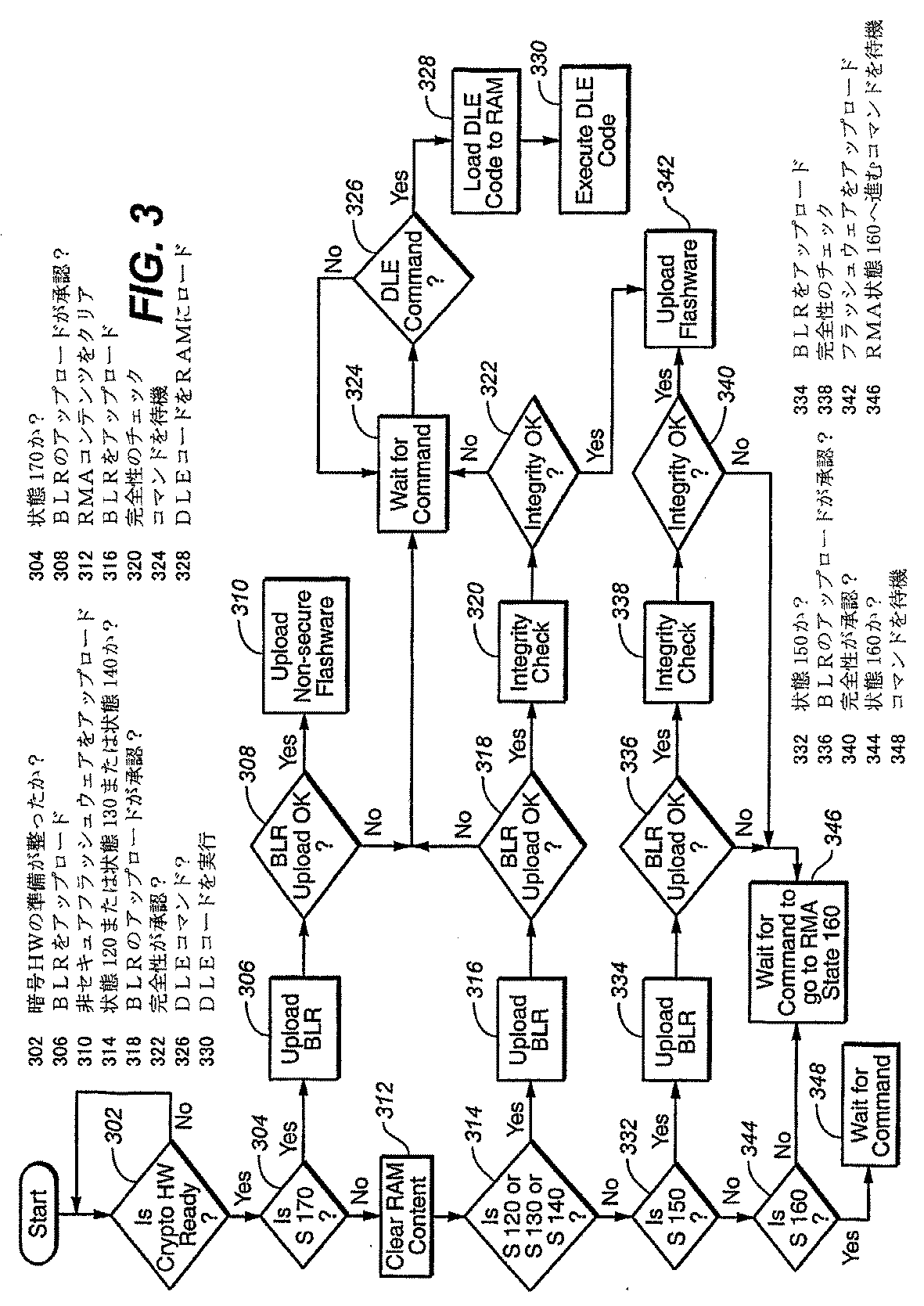
図3は、前述したシステムを実行するメモリカード用の起動プロセスを示す。起動プロセスのさらなる情報に関しては、ミッキー・ホルツマンらによる同時係属出願中の米国特許出願第11/284,623号「メモリコントローラファームウェアのハードウェアドライバの完全性チェック方法」(代理人整理番号SNDK.408US1)(特許文献1)を参照されたい。この特許出願は、その全体が本願明細書において参照により援用されている。 FIG. 3 shows a boot process for a memory card that executes the system described above. For further information on the boot process, see Mickey Holtzman et al., Co-pending U.S. Patent Application No. 11 / 284,623, “How to Check Memory Driver Firmware Hardware Driver Integrity” (Attorney Docket No. SNDK.408US1). ) (Patent Document 1). This patent application is incorporated herein by reference in its entirety.
ステップ302において、システムは、暗号エンジン40および他の構成要素を含む暗号ハードウェアの準備が整っているかをチェックする。このシステムは、ハードウェアの準備が整うまで進行を待機する。ハードウェアの準備が整うと、システムは、ステップ304に進む。ステップ304において、システムは、カードが状態170、すなわち、無効化状態にあるかを確認するチェックを行う。カードが状態170にあれば、ステップ306において、システムは、フラッシュメモリ20からRAM11へ、最小量の始動コードである起動ローダ(「BLR」)をアップロードする。次に、ステップ308において、システムは、BLRが適切にアップロードされたかを確認するチェックを行う。アップロードされていれば、ステップ310において、システムは、非セキュアモードで走らせる必要のあるファームウェアをアップロードする(標準ファームウェアから暗号機能をなくす)。ステップ308において決定したように、BLRが適切にアップロードされていなければ、システムは、以下に説明するステップ324に進む。
In
ステップ304において、システムが、カードが状態170にないと決定すれば、システムは、ステップ312において、RAMコンテンツをクリアする。その後、システムは、ステップ314においてカードがどの状態にあるかを確認するチェックを再度行う。カードが状態120、130、または140にあれば、BLRは、ステップ316においてアップロードされる。ステップ318において、システムは、BLRが適切にアップロードされたかを確認するチェックを行う。次に、ステップ320において、BLRコードの完全性チェックが実行される。この完全性チェックは、メッセージ認証コード(MAC)値を計算し、その値を参照値と比較することによって実行されるハードウェアベースのチェックである。完全性チェックの結果は、メモリに格納された単純なフラグである。ステップ322において、ファームウェアは、完全性がベリファイされたか否かを確認するためにフラグをチェックする。完全性が承認されれば、システムは、ステップ342において、セキュアモードで走らせるのに必要なファームウェアをアップロードし、これにより、非セキュアデータを格納し取り出せることができることは言うまでもない。完全性が、ステップ322において決定されるように承認されなければ、システムは、ステップ324によって現されているように、ホストからのある命令をダウンロードし実行するために、ホストからの診断コマンド(DLEコマンド)を待機する。ステップ326から分かるように、DLEコマンドが受信されれば、システムは、ステップ328において、DLEコードをRAMにロードするために進む。ステップ330において、DLEコードは、コントローラによって実行される。
If, at
ステップ314において、カードが状態120、130、または140にないことが決定されれば、システムは、ステップ332において、カードが状態150にあるかを確認するチェックを行う。この状態にあれば、システムは、ステップ334において、BLRをアップロードする。これは、ROMコードによって行われる。ステップ336で決定されるように、BLRのアップロードが承認されれば、ステップ338において、ステップ320において前述したようなハードウェアベースの完全性チェックが実行される。このハードウェアベースの完全性チェックの後、ステップ340において、別の完全性チェック、この場合は、ソフトウェアベースの完全性チェックが実行される。完全性が承認されれば、システムは、ステップ342において、セキュアモードにおいて走らせる必要のあるファームウェアをアップロードし、これにより、非セキュアデータを格納し取り出すことができることは言うまでもない。
If in
ステップ332において、カードが状態150にないことが決定されれば、システムは、カードの状態およびカードが状態160にあるかをチェックし、この状態にあれば、システムは、ステップ348によって表される診断コマンドを待機する。しかし、ステップ344において、カードが状態160にないことが決定されれば、システムは、ステップ346から分かるように、RMA状態160に進むためのコマンドを待機する。
If it is determined in
Claims (29)
前記メモリカードがテストポートを設けたメモリダイとセキュリティシステムを含み、前記メモリカードがテスト状態、動作状態、故障解析状態、および無効化状態中に動作可能であり、前記セキュリティシステムが暗号化エンジンおよび暗号鍵を含み、
テスト状態中に、前記テストポートがハードウェアテスト用に利用可能であり、かつ前記暗号化エンジンの動作および前記メモリカードのソフトウェアのテストを有効化するソフトウェアテストルーチンが利用可能であり、
動作状態中に、前記テストポートが利用不能であり、前記ソフトウェアテストルーチンが利用不能であり、かつ前記メモリカードがセキュアメモリカードとして動作するように構成され、
無効化状態中に、無効化状態が不可逆的であり、前記暗号化エンジンが無効化され、かつ前記メモリカードが非セキュアメモリカードとして動作し、
ホストが前記メモリカードに接続された時に、
前記メモリカードが前記テスト状態にある間に前記メモリカードのソフトウェアをテストするステップと、
前記テスト状態から前記動作状態に前記メモリカードを不可逆的に切り替えるコマンドを、前記メモリカードに送信するステップと、
前記メモリカードの故障を検出すると、前記メモリカードのソフトウェアおよびハードウェアのテストを有効化し、前記メモリカードが前記メモリカード上のすでに格納された情報を再度復号化するかあるいはセキュア動作状態に入ることを防ぎ、かつ前記メモリカードが無効化状態への遷移だけができるように前記メモリカードを構成するように、故障解析状態中に前記メモリカードを動作させるステップと、
を前記ホストが実行することを含む方法。A memory card operating method ,
The memory card includes a memory die provided with a test port and a security system, the memory card is operable in a test state, an operation state, a failure analysis state, and an invalidation state, and the security system includes an encryption engine and a cipher Including the key
During test state, the test port is available for hardware testing, and Ri operation and the software test routines to enable testing of the memory card software available Der of the encryption engine,
During operation state is the test port is unavailable, the software testing routine Ri impossible der utilized and the memory card is configured to operate as a secure memory card,
During the disabled state, the disabled state is irreversible, the encryption engine is disabled, and the memory card operates as a non-secure memory card,
When the host is connected to the memory card,
Testing the memory card software while the memory card is in the test state ;
And transmitting the irreversibly switched commands the memory card to the operating state from the test state, before Symbol memory card,
Upon detecting a failure of the memory card, the software and hardware test of the memory card is validated, and the memory card again decrypts information already stored on the memory card or enters a secure operating state And operating the memory card during a failure analysis state to configure the memory card so that the memory card can only transition to an invalidation state;
Wherein the host executes .
前記メモリカードの現在の状態を示すインジケータが、前記メモリカードの不揮発性メモリに格納される方法。The method of claim 1 , wherein
A method in which an indicator indicating the current state of the memory card is stored in a non-volatile memory of the memory card .
前記故障解析状態中に前記メモリカードを動作させるステップにより、前記メモリカードが新しい鍵の値を故障解析状態中の起動時ごとに生成し、直近の起動前に暗号化されたデータを前記メモリカードが復号化することができない方法。By operating the memory card during the failure analysis state, the memory card generates a new key value at each startup in the failure analysis state, and the memory card generates data encrypted before the most recent startup. That can not be decrypted.
前記メモリカードに格納された情報を保護するために、情報を暗号化し、かつ復号化するように構成された暗号化エンジンと、
前記暗号化および復号化用に使用される前記メモリカードにある秘密鍵と、を備え、
テスト状態、セキュア動作状態、バイパス動作状態間の遷移に対して前記セキュリティシステムが動作可能であり、
前記テスト状態中に、
前記暗号化エンジンが有効化され、
テスト状態に入ると、前記秘密鍵が生成され、
前記メモリカードのファームウェアのテストが有効化され、
前記メモリカードのハードウェアのテストが有効化され、
前記セキュア動作状態中に、
前記メモリカードのファームウェアのテストが無効化され、
前記メモリカードのハードウェアのテストが無効化され、
前記暗号化エンジンが有効化され、
情報を暗号化および復号化するために、前記秘密鍵が前記暗号化エンジンによって使用され、
前記バイパス動作状態中に、
前記暗号化エンジンが無効化され、
前記メモリカードのハードウェアのテストが有効化され、
前記メモリカードのファームウェアのテストが有効化され、
レギュラーカードとして動作していれば、バイパス動作状態が使用され、バイパス動作状態になると、前記セキュリティシステムをセキュア動作状態に再度遷移することができないシステム。 A security system is realized either as operatively memory cards of the secure card or a regular card,
To protect the information stored in the memory card, and configured encryption engine to encrypt information, and decoding,
A secret key in the memory card used for the encryption and decryption ,
The security system is operable with respect to transitions between test state, secure operating state, bypass operating state;
During the test state,
The encryption engine is activated,
When entering the test state, the secret key is generated,
Firmware test of the memory card is enabled,
Hardware test of the memory card is enabled,
It said in a secure operating state,
Firmware test of the memory card is disabled,
Hardware test of the memory card is disabled,
The encryption engine is activated,
The secret key is used by the encryption engine to encrypt and decrypt information ;
During the bypass operating state,
The encryption engine is disabled,
Hardware test of the memory card is enabled,
Firmware test of the memory card is enabled,
If operating as a regular card, the bypass operation state is used, and when the bypass operation state is entered, the security system cannot transition to the secure operation state again .
前記メモリカードが、前記バイパス動作状態中に構成された非セキュアカードとして最初に販売されるシステム。The system of claim 4 , wherein
A system in which the memory card is initially sold as a non-secure card configured during the bypass operating state.
前記メモリカードが、前記セキュア動作状態中に構成されたセキュアカードとして最初に販売されるシステム。The system of claim 4 , wherein
A system in which the memory card is initially sold as a secure card configured during the secure operating state.
セキュアカードとして最初に販売された前記メモリカードが、製造業者に返品されると、前記バイパス動作状態にされるシステム。The system of claim 6 , wherein
A system in which the memory card that is initially sold as a secure card is put into the bypass operation state when returned to the manufacturer.
前記バイパス動作状態にされた後の前記メモリカードを、非セキュアカードとして販売するシステム。The system of claim 7 , wherein
A system for selling the memory card after the bypass operation state as a non-secure card.
前記暗号化エンジンが、ハードウェアベースのものであるシステム。The system of claim 4 , wherein
A system in which the encryption engine is hardware based.
前記秘密鍵が、前記暗号化エンジンの不揮発性メモリに格納されるシステム。The system of claim 4 , wherein
A system in which the secret key is stored in a non-volatile memory of the encryption engine.
前記メモリカードのハードウェアのテストが有効化され、
前記メモリカードのファームウェアのテストが有効化され、
故障解析状態中に前記システムが起動されるたびに、前記秘密鍵が再生成される、故障解析動作状態をさらに含むシステム。The system of claim 4 , wherein
Hardware test of the memory card is enabled,
Firmware test of the memory card is enabled,
A system further comprising a failure analysis operating state, wherein the secret key is regenerated each time the system is activated during a failure analysis state.
前記故障解析動作状態に入った後、前記メモリカードをセキュア動作状態で再度使用することができないシステム。The system of claim 11 , wherein
Wherein After entering the failure analysis operating state, it can not be used again the memory card in secure operating state system.
前記故障解析動作状態が、バイパス動作状態に入る前に作動されるシステム。The system of claim 12 , wherein
System the failure analysis operating state, which is activated prior to entering the bypass operating state.
前記テスト状態は、テストポートおよび前記メモリカードのファームウェアにあるテスト機構の使用が可能である、前記メモリカードのテスト中に利用可能な動作の1つ以上のテスト状態を含み、
前記セキュア動作状態は、テストポートおよび前記メモリカードのファームウェアにあるテスト機構の使用を禁止して、前記メモリカードの通常使用中に利用可能であり、
前記メモリカードは、前記1つ以上のテスト状態のうちの1つのテスト状態とセキュア動作状態との間を切り替えるための論理をさらに備え、前記メモリカードがセキュア状態に切り替えられると、前記1つ以上のテスト状態に再度アクセスすることはできず、前記ファームウェアにあるテスト機構および前記テストポートへのアクセスを防ぐことによって、前記メモリカード上のセキュアデータへのアクセスを禁止するシステム。 The system of claim 4, wherein
The test conditions, the use of firmware near Rute strike mechanism Te Sutopoto and the memory card are possible, including one or more test conditions of available operations during testing of the memory card,
The secure operating state, prohibit the use of firmware near Rute strike mechanism Te Sutopoto and the memory card are available during normal use of the memory card,
The memory card may further comprising one or more logic for switching between one test state and secure operation state of the test conditions, when switched to the memory card Gase cure state, the can not be re-access one or more test conditions, by preventing access to the firmware near ruthenate strike mechanism and the test port, Cie to prevent access to the secure data on the memory card Stem.
故障解析状態をさらに備え、データを暗号化および復号化するために使用される新しい鍵が起動時ごとに生成され、ある鍵で暗号化されたデータを別の鍵で復号化することができないシステム。The system of claim 14 , wherein
Failure analysis state further comprising a new key used to encrypt and decrypt the data is generated for each time of startup, it is impossible to decrypt the encrypted data in a certain key on another key system.
バイパス動作状態に入る前に、前記故障解析状態に入るシステム。The system of claim 15 , wherein
Prior to entering the bypass operating conditions, the system entering the failure analysis state.
セキュア動作状態中に使用される最終ファームウェアを前記メモリカードにロードするために使用される最終鍵状態をさらに備え、前記最終ファームウェアにあるテスト機構が前記最終鍵状態中に無効化されるシステム。The system of claim 14 , wherein
Se further comprising a final key state used to load the final firmware used during cure operation state to the memory card, the final firmware near ruthenate strike mechanism is disabled during the final key state system.
前記最終鍵状態中に、前記テストポートとの通信が利用不能になるシステム。The system of claim 17 , wherein
A system in which communication with the test port becomes unavailable during the final key state.
セキュアカードまたは非セキュアカードのいずれかを生産するために使用可能な前記メモリカードに実現されるセキュリティシステムと、
前記メモリカードに格納された情報を保護するために、情報を暗号化および復号化するように設計された暗号化エンジンと、
テスト状態であって、
前記暗号化エンジンが有効化され、
前記メモリカードのファームウェアがテストされてもよく、
前記メモリカードのハードウェアがテストされてもよい、テスト状態と、
セキュア動作状態であって、
前記メモリカードのファームウェアがテスト不能であり、
前記メモリカードのハードウェアがテスト不能であり、
前記暗号化エンジンが有効化される、セキュア動作状態と、
前記暗号化エンジンが無効化されるバイパス動作状態と、
を備えるメモリカード。 A memory card,
A security system implemented in the memory card that can be used to produce either a secure card or a non-secure card; and
To protect the information stored in the memory card, the encryption engine designed to encrypt and decrypt information,
In a test state,
The encryption engine is activated,
The memory card firmware may be tested,
A test state in which the memory card hardware may be tested; and
A secure operating state,
The firmware of the memory card is untestable,
The memory card hardware is untestable;
A secure operating state in which the encryption engine is enabled; and
A bypass operating state in which the encryption engine is disabled;
A memory card.
前記バイパス動作状態中に、
前記メモリカードのハードウェアがテスト可能であり、
前記メモリカードのファームウェアがテスト可能であるメモリカード。The memory card according to claim 19 ,
During the bypass operation state,
The memory card hardware is testable;
A memory card in which firmware of the memory card can be tested.
最終鍵状態をさらに備え、
セキュア動作状態で使用される最終鍵が前記メモリカードで利用され、
前記メモリカードが構成可能であり、
前記メモリカードのハードウェアテスト機構がテスト不能であり、
前記メモリカードのソフトウェアテスト機構がテスト不能であるメモリカード。The memory card according to claim 19 ,
A final key state ,
The final key to be used in a secure operating state is utilized in the previous Symbol memory card,
The memory card is configurable;
The hardware test mechanism of the memory card is untestable,
A memory card whose software test mechanism is not testable.
前記メモリカードに格納されたデータを暗号化および復号化する暗号化エンジンと、
前記暗号化エンジンを使用して暗号化および復号化を有効化する第1の鍵を生成する前記メモリカードをテストする第1の動作状態と、
前記メモリカードに格納されたデータを暗号化および復号化するために第2の鍵を利用する前記メモリカードの消費者使用のための第2の動作状態と、
前記暗号化エンジンの動作が無効化され、前記メモリカードのハードウェアのテストが有効化され、かつ前記メモリカードのファームウェアのテストが有効化される、バイパス動作状態を規定する第3の動作状態と、
を備え、
第2の動作状態から遷移した後で第2の動作状態に前記メモリカードが再度入ることができないように、前記メモリカードを構成し、
前記第1の鍵で暗号化されたデータが前記第2の鍵で復号化できず、前記第2の鍵で暗号化されたデータが前記第1の鍵で復号化できず、
前記暗号化エンジンを第1の動作状態でテスト可能であるが、前記メモリカードが第1の動作状態にある間の暗号化されたデータを、前記メモリカードが第2の動作状態にある間に読み出すことはできないメモリカード。 A flash memory card,
An encryption engine for encrypting and decrypting data stored in the memory card;
A first operating state that tests the memory card to generate a first key that enables encryption and decryption using the encryption engine;
A second operating state for consumer use of the memory card to use the second key to encrypt and decrypt data stored in the memory card,
A third operating state defining a bypass operating state, wherein the operation of the encryption engine is disabled, the memory card hardware test is enabled, and the memory card firmware test is enabled; ,
With
Configuring the memory card so that the memory card cannot re-enter the second operating state after transitioning from the second operating state;
First key encrypted data previously in SL can not be decrypted with a second key, the encrypted data in the second key can not be decrypted before Symbol first key,
Although the encryption engine can be tested in a first operating state, the memory card is encrypted while in the first operating state data, while the memory card is in the second operating state memory card can not Succoth read out.
前記第1の鍵の値が、前記メモリカードが起動されるたびに変更されるメモリカード。The memory card according to claim 22 ,
A memory card in which the value of the first key is changed each time the memory card is activated.
前記第1の鍵の値が、一定であるメモリカード。The memory card according to claim 22 ,
A memory card in which the value of the first key is constant.
前記第1の鍵の値が、前記第1の動作状態に入るたびに一度再生成されるメモリカード。The memory card according to claim 22 ,
A memory card in which the value of the first key is regenerated once every time the first operating state is entered.
前記第2の鍵の値が一定であり、前記メモリカードの不揮発性メモリに格納されるメモリカード。The memory card according to claim 22 ,
A memory card in which a value of the second key is constant and stored in a nonvolatile memory of the memory card.
前記第2の鍵の値が、前記第1の動作状態の間にメモリに最後に格納される前記第1の鍵の値と等しいメモリカード。27. The memory card according to claim 26 .
A memory card wherein the value of the second key is equal to the value of the first key stored last in memory during the first operating state.
前記第1の動作状態中に、テストのためのハードウェアおよびファームウェアテスト機構が利用可能であるメモリカード。The memory card according to claim 22 ,
During said first operational state, the memory card hardware and firmware test mechanisms for testing is available.
前記第2の動作状態中に、テストのためのハードウェアおよびファームウェアテスト機構が利用不能であるメモリカード。The memory card according to claim 22 ,
A memory card in which hardware and firmware test mechanisms for testing are not available during the second operating state.
Applications Claiming Priority (7)
| Application Number | Priority Date | Filing Date | Title |
|---|---|---|---|
| US65112805P | 2005-02-07 | 2005-02-07 | |
| US60/651,128 | 2005-02-07 | ||
| US11/317,862 | 2005-12-22 | ||
| US11/317,390 | 2005-12-22 | ||
| US11/317,390 US8108691B2 (en) | 2005-02-07 | 2005-12-22 | Methods used in a secure memory card with life cycle phases |
| US11/317,862 US8321686B2 (en) | 2005-02-07 | 2005-12-22 | Secure memory card with life cycle phases |
| PCT/US2006/003876 WO2006086232A2 (en) | 2005-02-07 | 2006-02-01 | Secure memory card with life cycle phases |
Publications (2)
| Publication Number | Publication Date |
|---|---|
| JP2008530659A JP2008530659A (en) | 2008-08-07 |
| JP4787273B2 true JP4787273B2 (en) | 2011-10-05 |
Family
ID=36644859
Family Applications (1)
| Application Number | Title | Priority Date | Filing Date |
|---|---|---|---|
| JP2007554249A Expired - Fee Related JP4787273B2 (en) | 2005-02-07 | 2006-02-01 | Secure memory card with life cycle phase |
Country Status (7)
| Country | Link |
|---|---|
| EP (1) | EP1846826A2 (en) |
| JP (1) | JP4787273B2 (en) |
| KR (1) | KR100972540B1 (en) |
| CN (1) | CN101164048B (en) |
| IL (1) | IL184793A0 (en) |
| TW (1) | TWI402755B (en) |
| WO (1) | WO2006086232A2 (en) |
Families Citing this family (10)
| Publication number | Priority date | Publication date | Assignee | Title |
|---|---|---|---|---|
| US7748031B2 (en) | 2005-07-08 | 2010-06-29 | Sandisk Corporation | Mass storage device with automated credentials loading |
| US8966284B2 (en) | 2005-09-14 | 2015-02-24 | Sandisk Technologies Inc. | Hardware driver integrity check of memory card controller firmware |
| US8070057B2 (en) | 2007-09-12 | 2011-12-06 | Devicefidelity, Inc. | Switching between internal and external antennas |
| US9311766B2 (en) | 2007-09-12 | 2016-04-12 | Devicefidelity, Inc. | Wireless communicating radio frequency signals |
| US8109444B2 (en) | 2007-09-12 | 2012-02-07 | Devicefidelity, Inc. | Selectively switching antennas of transaction cards |
| US8915447B2 (en) | 2007-09-12 | 2014-12-23 | Devicefidelity, Inc. | Amplifying radio frequency signals |
| US9304555B2 (en) | 2007-09-12 | 2016-04-05 | Devicefidelity, Inc. | Magnetically coupling radio frequency antennas |
| US9553721B2 (en) * | 2015-01-30 | 2017-01-24 | Qualcomm Incorporated | Secure execution environment communication |
| LU503412B1 (en) * | 2023-01-31 | 2024-08-01 | Elmos Semiconductor Se | CONTROL SYSTEM, CONTROL DEVICE AND METHOD FOR PROVIDING A CONTROL AND/OR REGULATING SIGNAL |
| CN116230065A (en) * | 2023-02-14 | 2023-06-06 | 北京国家新能源汽车技术创新中心有限公司 | Method for testing erasing life of embedded nonvolatile memory of security chip, storage medium and computer |
Citations (5)
| Publication number | Priority date | Publication date | Assignee | Title |
|---|---|---|---|---|
| JPH09198316A (en) * | 1996-01-22 | 1997-07-31 | Toshiba Corp | Data protection circuit |
| JPH11161549A (en) * | 1997-11-28 | 1999-06-18 | Toshiba Corp | Secret information management method and system for portable information equipment |
| JP2000172821A (en) * | 1998-12-10 | 2000-06-23 | Toshiba Corp | Semiconductor device, data storage medium, data recording device, data reading device, and method of manufacturing semiconductor device |
| JP2003337749A (en) * | 2002-03-13 | 2003-11-28 | Matsushita Electric Ind Co Ltd | Secure device |
| WO2005010808A2 (en) * | 2003-07-17 | 2005-02-03 | Sandisk Corporation | Memory card with raised portion |
Family Cites Families (12)
| Publication number | Priority date | Publication date | Assignee | Title |
|---|---|---|---|---|
| DE4243888A1 (en) * | 1992-12-23 | 1994-06-30 | Gao Ges Automation Org | Data carrier and method for checking the authenticity of a data carrier |
| FR2716989B1 (en) * | 1994-03-04 | 1996-04-05 | Gemplus Card Int | Method of operation of a smart card. |
| EP1004992A3 (en) * | 1997-03-24 | 2001-12-05 | Visa International Service Association | A system and method for a multi-application smart card which can facilitate a post-issuance download of an application onto the smart card |
| WO1999064996A1 (en) * | 1998-06-05 | 1999-12-16 | Landis & Gyr Communications S.A.R.L. | Preloaded ic-card and method for authenticating the same |
| EP0992809A1 (en) * | 1998-09-28 | 2000-04-12 | Siemens Aktiengesellschaft | Circuit with deactivatable scan path |
| US7023996B2 (en) * | 2001-05-04 | 2006-04-04 | The Boeing Company | Encryption for asymmetric data links |
| DE10162306A1 (en) * | 2001-12-19 | 2003-07-03 | Philips Intellectual Property | Method and arrangement for verifying NV fuses as well as a corresponding computer program product and a corresponding computer-readable storage medium |
| US6912633B2 (en) * | 2002-03-18 | 2005-06-28 | Sun Microsystems, Inc. | Enhanced memory management for portable devices |
| US6843423B2 (en) * | 2003-03-13 | 2005-01-18 | Stmicroelectronics, Inc. | Smart card that can be configured for debugging and software development using secondary communication port |
| US6783078B1 (en) * | 2003-05-09 | 2004-08-31 | Stmicroelectronics, Inc. | Universal serial bus (USB) smart card having read back testing features and related system, integrated circuit, and methods |
| TW200501281A (en) * | 2003-06-27 | 2005-01-01 | Kingpak Tech Inc | Manufacturing method of small memory card having display |
| TWI223974B (en) * | 2003-11-20 | 2004-11-11 | Advanced Semiconductor Eng | Tiny memory card and method for manufacturing the same |
-
2006
- 2006-02-01 KR KR1020077018143A patent/KR100972540B1/en not_active Expired - Fee Related
- 2006-02-01 JP JP2007554249A patent/JP4787273B2/en not_active Expired - Fee Related
- 2006-02-01 WO PCT/US2006/003876 patent/WO2006086232A2/en not_active Ceased
- 2006-02-01 EP EP06734304A patent/EP1846826A2/en not_active Withdrawn
- 2006-02-01 CN CN2006800042296A patent/CN101164048B/en not_active Expired - Fee Related
- 2006-02-07 TW TW095104117A patent/TWI402755B/en not_active IP Right Cessation
-
2007
- 2007-07-23 IL IL184793A patent/IL184793A0/en not_active IP Right Cessation
Patent Citations (5)
| Publication number | Priority date | Publication date | Assignee | Title |
|---|---|---|---|---|
| JPH09198316A (en) * | 1996-01-22 | 1997-07-31 | Toshiba Corp | Data protection circuit |
| JPH11161549A (en) * | 1997-11-28 | 1999-06-18 | Toshiba Corp | Secret information management method and system for portable information equipment |
| JP2000172821A (en) * | 1998-12-10 | 2000-06-23 | Toshiba Corp | Semiconductor device, data storage medium, data recording device, data reading device, and method of manufacturing semiconductor device |
| JP2003337749A (en) * | 2002-03-13 | 2003-11-28 | Matsushita Electric Ind Co Ltd | Secure device |
| WO2005010808A2 (en) * | 2003-07-17 | 2005-02-03 | Sandisk Corporation | Memory card with raised portion |
Also Published As
| Publication number | Publication date |
|---|---|
| CN101164048A (en) | 2008-04-16 |
| EP1846826A2 (en) | 2007-10-24 |
| JP2008530659A (en) | 2008-08-07 |
| TWI402755B (en) | 2013-07-21 |
| TW200641696A (en) | 2006-12-01 |
| IL184793A0 (en) | 2008-01-20 |
| CN101164048B (en) | 2010-06-16 |
| KR20070121642A (en) | 2007-12-27 |
| WO2006086232A2 (en) | 2006-08-17 |
| KR100972540B1 (en) | 2010-07-28 |
| WO2006086232A3 (en) | 2007-10-11 |
Similar Documents
| Publication | Publication Date | Title |
|---|---|---|
| US8423788B2 (en) | Secure memory card with life cycle phases | |
| US8108691B2 (en) | Methods used in a secure memory card with life cycle phases | |
| CN115019874B (en) | Secure device status apparatus and method | |
| US8572410B1 (en) | Virtualized protected storage | |
| JP5984625B2 (en) | Semiconductor device and encryption key writing method | |
| US8321686B2 (en) | Secure memory card with life cycle phases | |
| TWI483139B (en) | Secure key storage using physically unclonable functions | |
| CN101256613B (en) | Secure processor system that does not require maker and user to know each other's encrypted information | |
| CN101263501B (en) | Hard Drive Integrity Check for Memory Card Controller Firmware | |
| US20070237325A1 (en) | Method and apparatus to improve security of cryptographic systems | |
| US20080107275A1 (en) | Method and system for encryption of information stored in an external nonvolatile memory | |
| US20080148118A1 (en) | Method and system for protecting processors from unauthorized debug access | |
| US20070297606A1 (en) | Multiple key security and method for electronic devices | |
| CN102027707A (en) | Integrated circuit with secured software image and method therefor | |
| US20060198515A1 (en) | Secure disc drive electronics implementation | |
| US9152576B2 (en) | Mode-based secure microcontroller | |
| JP4787273B2 (en) | Secure memory card with life cycle phase | |
| US11481523B2 (en) | Secure element | |
| CN112069551A (en) | Electronic circuit | |
| JP4791250B2 (en) | Microcomputer and its software falsification prevention method | |
| CN101799789B (en) | Chip and memory data protection device and protection method thereof | |
| CN109583196B (en) | Key generation method | |
| CN102236754B (en) | Data security method and electronic device using the data security method | |
| Brych et al. | FIPS 140-2 Level 3 Non-Proprietary Security Policy |
Legal Events
| Date | Code | Title | Description |
|---|---|---|---|
| A977 | Report on retrieval |
Free format text: JAPANESE INTERMEDIATE CODE: A971007 Effective date: 20101007 |
|
| A131 | Notification of reasons for refusal |
Free format text: JAPANESE INTERMEDIATE CODE: A131 Effective date: 20101019 |
|
| A601 | Written request for extension of time |
Free format text: JAPANESE INTERMEDIATE CODE: A601 Effective date: 20110112 |
|
| A602 | Written permission of extension of time |
Free format text: JAPANESE INTERMEDIATE CODE: A602 Effective date: 20110119 |
|
| A601 | Written request for extension of time |
Free format text: JAPANESE INTERMEDIATE CODE: A601 Effective date: 20110215 |
|
| A602 | Written permission of extension of time |
Free format text: JAPANESE INTERMEDIATE CODE: A602 Effective date: 20110222 |
|
| A601 | Written request for extension of time |
Free format text: JAPANESE INTERMEDIATE CODE: A601 Effective date: 20110315 |
|
| A602 | Written permission of extension of time |
Free format text: JAPANESE INTERMEDIATE CODE: A602 Effective date: 20110323 |
|
| A521 | Request for written amendment filed |
Free format text: JAPANESE INTERMEDIATE CODE: A523 Effective date: 20110419 |
|
| TRDD | Decision of grant or rejection written | ||
| A01 | Written decision to grant a patent or to grant a registration (utility model) |
Free format text: JAPANESE INTERMEDIATE CODE: A01 Effective date: 20110621 |
|
| A01 | Written decision to grant a patent or to grant a registration (utility model) |
Free format text: JAPANESE INTERMEDIATE CODE: A01 |
|
| A61 | First payment of annual fees (during grant procedure) |
Free format text: JAPANESE INTERMEDIATE CODE: A61 Effective date: 20110714 |
|
| R150 | Certificate of patent or registration of utility model |
Free format text: JAPANESE INTERMEDIATE CODE: R150 |
|
| FPAY | Renewal fee payment (event date is renewal date of database) |
Free format text: PAYMENT UNTIL: 20140722 Year of fee payment: 3 |
|
| R250 | Receipt of annual fees |
Free format text: JAPANESE INTERMEDIATE CODE: R250 |
|
| R250 | Receipt of annual fees |
Free format text: JAPANESE INTERMEDIATE CODE: R250 |
|
| R250 | Receipt of annual fees |
Free format text: JAPANESE INTERMEDIATE CODE: R250 |
|
| LAPS | Cancellation because of no payment of annual fees |