JP4780117B2 - Angle sensor, manufacturing method thereof, and angle detection device using the same - Google Patents
Angle sensor, manufacturing method thereof, and angle detection device using the same Download PDFInfo
- Publication number
- JP4780117B2 JP4780117B2 JP2008019647A JP2008019647A JP4780117B2 JP 4780117 B2 JP4780117 B2 JP 4780117B2 JP 2008019647 A JP2008019647 A JP 2008019647A JP 2008019647 A JP2008019647 A JP 2008019647A JP 4780117 B2 JP4780117 B2 JP 4780117B2
- Authority
- JP
- Japan
- Prior art keywords
- sensor
- film
- ferromagnetic
- angle
- layer
- Prior art date
- Legal status (The legal status is an assumption and is not a legal conclusion. Google has not performed a legal analysis and makes no representation as to the accuracy of the status listed.)
- Active
Links
- 238000001514 detection method Methods 0.000 title claims description 18
- 238000004519 manufacturing process Methods 0.000 title claims description 17
- 230000005291 magnetic effect Effects 0.000 claims description 222
- 230000005415 magnetization Effects 0.000 claims description 145
- 230000005294 ferromagnetic effect Effects 0.000 claims description 143
- 230000000694 effects Effects 0.000 claims description 59
- 238000010438 heat treatment Methods 0.000 claims description 39
- 230000008878 coupling Effects 0.000 claims description 36
- 238000010168 coupling process Methods 0.000 claims description 36
- 238000005859 coupling reaction Methods 0.000 claims description 36
- 238000000034 method Methods 0.000 claims description 32
- 239000000758 substrate Substances 0.000 claims description 19
- 230000008569 process Effects 0.000 claims description 10
- 230000008034 disappearance Effects 0.000 claims description 6
- 230000006698 induction Effects 0.000 claims description 4
- 230000007246 mechanism Effects 0.000 claims description 4
- 238000000059 patterning Methods 0.000 claims description 4
- 229910000531 Co alloy Inorganic materials 0.000 claims 2
- 229910000640 Fe alloy Inorganic materials 0.000 claims 1
- 239000010408 film Substances 0.000 description 196
- 239000010410 layer Substances 0.000 description 165
- XEEYBQQBJWHFJM-UHFFFAOYSA-N iron Substances [Fe] XEEYBQQBJWHFJM-UHFFFAOYSA-N 0.000 description 26
- 230000005290 antiferromagnetic effect Effects 0.000 description 19
- 239000000203 mixture Substances 0.000 description 19
- 239000010409 thin film Substances 0.000 description 18
- 230000007423 decrease Effects 0.000 description 16
- 229910020598 Co Fe Inorganic materials 0.000 description 14
- 229910002519 Co-Fe Inorganic materials 0.000 description 14
- 230000008859 change Effects 0.000 description 14
- 229910052742 iron Inorganic materials 0.000 description 14
- 238000005259 measurement Methods 0.000 description 13
- 230000002829 reductive effect Effects 0.000 description 13
- 238000004458 analytical method Methods 0.000 description 11
- 238000010586 diagram Methods 0.000 description 10
- 230000000903 blocking effect Effects 0.000 description 6
- 239000010949 copper Substances 0.000 description 6
- 238000009812 interlayer coupling reaction Methods 0.000 description 5
- 239000000463 material Substances 0.000 description 5
- 229910052751 metal Inorganic materials 0.000 description 5
- 239000002184 metal Substances 0.000 description 5
- 229910045601 alloy Inorganic materials 0.000 description 4
- 239000000956 alloy Substances 0.000 description 4
- 230000015572 biosynthetic process Effects 0.000 description 4
- 230000003247 decreasing effect Effects 0.000 description 4
- 230000005389 magnetism Effects 0.000 description 4
- 238000001816 cooling Methods 0.000 description 3
- 238000005516 engineering process Methods 0.000 description 3
- 230000000704 physical effect Effects 0.000 description 3
- 230000001681 protective effect Effects 0.000 description 3
- 238000012887 quadratic function Methods 0.000 description 3
- 230000009467 reduction Effects 0.000 description 3
- XKRFYHLGVUSROY-UHFFFAOYSA-N Argon Chemical compound [Ar] XKRFYHLGVUSROY-UHFFFAOYSA-N 0.000 description 2
- 229910003321 CoFe Inorganic materials 0.000 description 2
- 229910001030 Iron–nickel alloy Inorganic materials 0.000 description 2
- 239000003302 ferromagnetic material Substances 0.000 description 2
- 239000012528 membrane Substances 0.000 description 2
- RYGMFSIKBFXOCR-UHFFFAOYSA-N Copper Chemical compound [Cu] RYGMFSIKBFXOCR-UHFFFAOYSA-N 0.000 description 1
- 229910000599 Cr alloy Inorganic materials 0.000 description 1
- 229910017061 Fe Co Inorganic materials 0.000 description 1
- 229910002546 FeCo Inorganic materials 0.000 description 1
- KJTLSVCANCCWHF-UHFFFAOYSA-N Ruthenium Chemical compound [Ru] KJTLSVCANCCWHF-UHFFFAOYSA-N 0.000 description 1
- 230000005856 abnormality Effects 0.000 description 1
- 239000002885 antiferromagnetic material Substances 0.000 description 1
- 229910052786 argon Inorganic materials 0.000 description 1
- 238000004364 calculation method Methods 0.000 description 1
- 239000000788 chromium alloy Substances 0.000 description 1
- BIJOYKCOMBZXAE-UHFFFAOYSA-N chromium iron nickel Chemical compound [Cr].[Fe].[Ni] BIJOYKCOMBZXAE-UHFFFAOYSA-N 0.000 description 1
- 229910052802 copper Inorganic materials 0.000 description 1
- 239000006185 dispersion Substances 0.000 description 1
- 238000009429 electrical wiring Methods 0.000 description 1
- 239000007772 electrode material Substances 0.000 description 1
- 238000001803 electron scattering Methods 0.000 description 1
- 238000002474 experimental method Methods 0.000 description 1
- 230000005307 ferromagnetism Effects 0.000 description 1
- 230000004907 flux Effects 0.000 description 1
- 230000001771 impaired effect Effects 0.000 description 1
- 238000009413 insulation Methods 0.000 description 1
- 238000010030 laminating Methods 0.000 description 1
- WABPQHHGFIMREM-UHFFFAOYSA-N lead(0) Chemical compound [Pb] WABPQHHGFIMREM-UHFFFAOYSA-N 0.000 description 1
- 230000007774 longterm Effects 0.000 description 1
- 238000001755 magnetron sputter deposition Methods 0.000 description 1
- 230000000149 penetrating effect Effects 0.000 description 1
- 229920002120 photoresistant polymer Polymers 0.000 description 1
- 230000002441 reversible effect Effects 0.000 description 1
- 229910052707 ruthenium Inorganic materials 0.000 description 1
- 229920006395 saturated elastomer Polymers 0.000 description 1
- 230000035945 sensitivity Effects 0.000 description 1
- 238000005477 sputtering target Methods 0.000 description 1
- 230000003068 static effect Effects 0.000 description 1
- 229910052715 tantalum Inorganic materials 0.000 description 1
- GUVRBAGPIYLISA-UHFFFAOYSA-N tantalum atom Chemical compound [Ta] GUVRBAGPIYLISA-UHFFFAOYSA-N 0.000 description 1
- 230000009466 transformation Effects 0.000 description 1
- 230000007704 transition Effects 0.000 description 1
- 230000002618 waking effect Effects 0.000 description 1
Images


Classifications
-
- G—PHYSICS
- G01—MEASURING; TESTING
- G01R—MEASURING ELECTRIC VARIABLES; MEASURING MAGNETIC VARIABLES
- G01R33/00—Arrangements or instruments for measuring magnetic variables
- G01R33/02—Measuring direction or magnitude of magnetic fields or magnetic flux
- G01R33/06—Measuring direction or magnitude of magnetic fields or magnetic flux using galvano-magnetic devices
- G01R33/09—Magnetoresistive devices
- G01R33/093—Magnetoresistive devices using multilayer structures, e.g. giant magnetoresistance sensors
-
- B—PERFORMING OPERATIONS; TRANSPORTING
- B82—NANOTECHNOLOGY
- B82Y—SPECIFIC USES OR APPLICATIONS OF NANOSTRUCTURES; MEASUREMENT OR ANALYSIS OF NANOSTRUCTURES; MANUFACTURE OR TREATMENT OF NANOSTRUCTURES
- B82Y25/00—Nanomagnetism, e.g. magnetoimpedance, anisotropic magnetoresistance, giant magnetoresistance or tunneling magnetoresistance
-
- G—PHYSICS
- G01—MEASURING; TESTING
- G01R—MEASURING ELECTRIC VARIABLES; MEASURING MAGNETIC VARIABLES
- G01R33/00—Arrangements or instruments for measuring magnetic variables
- G01R33/02—Measuring direction or magnitude of magnetic fields or magnetic flux
- G01R33/06—Measuring direction or magnitude of magnetic fields or magnetic flux using galvano-magnetic devices
- G01R33/09—Magnetoresistive devices
- G01R33/098—Magnetoresistive devices comprising tunnel junctions, e.g. tunnel magnetoresistance sensors
-
- Y—GENERAL TAGGING OF NEW TECHNOLOGICAL DEVELOPMENTS; GENERAL TAGGING OF CROSS-SECTIONAL TECHNOLOGIES SPANNING OVER SEVERAL SECTIONS OF THE IPC; TECHNICAL SUBJECTS COVERED BY FORMER USPC CROSS-REFERENCE ART COLLECTIONS [XRACs] AND DIGESTS
- Y10—TECHNICAL SUBJECTS COVERED BY FORMER USPC
- Y10T—TECHNICAL SUBJECTS COVERED BY FORMER US CLASSIFICATION
- Y10T29/00—Metal working
- Y10T29/49—Method of mechanical manufacture
- Y10T29/49002—Electrical device making
- Y10T29/4902—Electromagnet, transformer or inductor
- Y10T29/49021—Magnetic recording reproducing transducer [e.g., tape head, core, etc.]
- Y10T29/49032—Fabricating head structure or component thereof
- Y10T29/49034—Treating to affect magnetic properties
Landscapes
- Physics & Mathematics (AREA)
- Condensed Matter Physics & Semiconductors (AREA)
- General Physics & Mathematics (AREA)
- Chemical & Material Sciences (AREA)
- Engineering & Computer Science (AREA)
- Nanotechnology (AREA)
- Crystallography & Structural Chemistry (AREA)
- Hall/Mr Elements (AREA)
- Measuring Magnetic Variables (AREA)
- Transmission And Conversion Of Sensor Element Output (AREA)
- Measurement Of Length, Angles, Or The Like Using Electric Or Magnetic Means (AREA)
Description
本発明は、磁気抵抗効果センサを用いた角度センサとその製造方法、及びその角度センサを用いた非接触式角度検知装置に関するものである。 The present invention relates to an angle sensor using a magnetoresistive effect sensor, a manufacturing method thereof, and a non-contact type angle detection device using the angle sensor.
磁気による非接触式角度検出装置は、磁石と磁気センサなどを用いて、駆動体や回転体の角度を測ることの用に供される技術である。磁気センサ部に用いられる磁気抵抗効果膜として、異方性磁気抵抗効果のある磁性薄膜や、強磁性金属層を非磁性金属層を介して積層した多層膜のいわゆる巨大磁気抵抗、その他、トンネル磁気抵抗効果などが知られている。磁気ヘッドの再生センサとして用いられる同様の技術としてスピンバルブ膜があり、これは巨大磁気抵抗効果を感度よく得られる技術として知られている。スピンバルブ膜には、その磁化が感知すべき磁界に対して実質的に固定された強磁性固定層と、感知すべき磁化に対してスムーズに磁化回転する軟磁性自由層とを有し、両者の磁化の相対角度に応じた電気信号を出力する。 The non-contact type angle detection device using magnetism is a technique provided for measuring the angle of a driving body or a rotating body using a magnet and a magnetic sensor. The magnetoresistive film used in the magnetic sensor part is a magnetic thin film with anisotropic magnetoresistive effect, a so-called giant magnetoresistance of a multilayer film in which a ferromagnetic metal layer is laminated via a nonmagnetic metal layer, and other tunnel magnetism. The resistance effect is known. A similar technique used as a reproduction sensor for a magnetic head is a spin valve film, which is known as a technique that can obtain a giant magnetoresistance effect with high sensitivity. The spin valve film has a ferromagnetic fixed layer whose magnetization is substantially fixed with respect to the magnetic field to be sensed, and a soft magnetic free layer that smoothly rotates with respect to the magnetization to be sensed. An electric signal corresponding to the relative angle of the magnetization of is output.
磁気抵抗効果を用いたセンサは、角度検出装置用角度センサとして検討が行われてはきたが、従来の技術では、近年角度検出装置に要求される高温での安定動作と高い精度を実現することが困難であった。 Sensors using the magnetoresistive effect have been studied as angle sensors for angle detection devices. However, with conventional technology, stable operation at high temperatures and high accuracy required for angle detection devices in recent years have been achieved. It was difficult.
従来の角度検出装置において磁気抵抗効果センサで高温安定性と高い精度を実現しようとする際の欠点は、スピンバルブ膜の高温安定性に制限される点である。スピンバルブ膜は高い出力を実現するために角度検出装置における有力な技術であるが、角度センサとして応用するために必須の要素として、その強磁性固定層の磁化の固定、がある。スピンバルブ膜が印加された磁界の角度を検出するためには上記強磁性固定層の磁化の固定方向を基準にした出力が必要である。通常、スピンバルブ膜と呼ばれる技術では、この強磁性固定層の磁化の固定は、反強磁性膜を強磁性固定層に積層し、発生した交換結合力で磁化方向を固定する。特許文献1には、ピン止め磁性層が反強磁性膜により磁化が固定される回転角検出センサの記載がある。
A drawback in achieving high temperature stability and high accuracy with a magnetoresistive sensor in a conventional angle detection device is that it is limited to the high temperature stability of the spin valve film. A spin valve film is a promising technique in an angle detection device in order to realize a high output. However, as an essential element for application as an angle sensor, there is fixing of magnetization of the ferromagnetic fixed layer. In order to detect the angle of the magnetic field to which the spin valve film is applied, an output based on the fixed direction of magnetization of the ferromagnetic fixed layer is required. Usually, in a technique called a spin valve film, the magnetization of the ferromagnetic fixed layer is fixed by laminating an antiferromagnetic film on the ferromagnetic fixed layer and fixing the magnetization direction by the generated exchange coupling force.
このような反強磁性膜による磁化方向の固定は、上述したスピンバルブ膜や、同様の原理を用いたトンネル磁気抵抗効果素子においてよく知られた方法である。反強磁性体にネール温度があるのと同様に、上記交換結合力にはブロッキング温度と呼ばれる高温限界温度があり、この温度に達すると交換結合力は実質的に消失する。また、交換結合力はブロッキング温度に向けて低下していく、ブロッキング温度より低くても、近傍の温度では交換結合力が不十分になり、スピンバルブ膜の角度センサとしての機能は十分な精度を発揮できずに失われてしまう。この現象は角度センサにスピンバルブ膜を用いた場合のみならず、トンネル磁気抵抗効果膜及び、CPP−GMR(垂直電流型巨大磁気抵抗効果)膜を用いた場合でも、反強磁性膜による交換結合力を応用していれば同様に言えることである。広く応用に供されている反強磁性膜としては、MnPt膜や、MnIr膜があるが、それぞれブロッキング温度は320℃、250℃程度であって、例えば200℃というような高い温度での角度検出装置への応用範囲を達成することはできない。なんとなれば、ブロッキング温度に達していなくても、長時間200℃という環境において磁界が印加される状態が続けば、反強磁性膜による交換結合力はしだいに設定された方向性を失って行くからである。 Such fixing of the magnetization direction by the antiferromagnetic film is a well-known method in the above-described spin valve film and tunnel magnetoresistive effect element using the same principle. Similar to the Neel temperature of antiferromagnetic materials, the exchange coupling force has a high temperature limit temperature called a blocking temperature, and when this temperature is reached, the exchange coupling force substantially disappears. In addition, the exchange coupling force decreases toward the blocking temperature. Even if the exchange coupling force is lower than the blocking temperature, the exchange coupling force becomes insufficient at a nearby temperature, and the function of the spin valve film as an angle sensor has sufficient accuracy. Lost without being able to demonstrate. This phenomenon occurs not only when the spin valve film is used for the angle sensor, but also when the tunnel magnetoresistive film and the CPP-GMR (vertical current type giant magnetoresistive effect) film are used. The same can be said if power is applied. Antiferromagnetic films that have been widely used include MnPt films and MnIr films. The blocking temperatures are about 320 ° C and 250 ° C, respectively. For example, angle detection at a high temperature such as 200 ° C. The range of application to the device cannot be achieved. Even if the blocking temperature has not been reached, if the magnetic field continues to be applied in an environment of 200 ° C. for a long time, the exchange coupling force due to the antiferromagnetic film gradually loses its set directionality. Because.
一方、反強磁性膜を用いた場合と同様の効果をもつ別の磁化固定方法として、特許文献2のように着磁された磁性膜を用いる方法や、特許文献3に記載されたAAFシステム(人工反強磁性システム)と呼称されている反強磁性的に結合することによって実質的に保磁力を高めた状態を作り出した積層した磁性膜を用いる方法がある。上記反強磁性的に結合した磁性膜を用いたセンサについては、特許文献4及び5に、磁気センサ及び磁気ヘッドについての記載がある。これらの方法は、基本的に強磁性材料の薄膜について着磁処理を行い、残留磁化の方向をセンサの動作角度の基準にすることによって達成されている。特許文献3には、センサの薄膜形成時に磁界を印加し、この方向にピン止めされた強磁性層を用いる技術の記載がある。
On the other hand, as another magnetization fixing method having the same effect as that using an antiferromagnetic film, a method using a magnetic film magnetized as in
磁気ヘッドに応用されるスピンバルブ膜には、反強磁性膜によらずに磁化方向を固定する技術として特許文献4、5及び非特許文献1に記載されている(自己ピン型、人工反強磁性システムなどとも呼ばれる)技術が知られている。これは、例えばCo/Ru/Coという積層構造を適切な厚さと作製方法で形成すると、2つのCo層が反強磁性的に強く交換結合し、結果、反平行配列した2つのCo層の磁化が外部磁界によって変化しにくくなることを応用した技術である。本明細書では、このようなシステムをセルフピン型と呼ぶことにする。一般的に、強磁性金属のキュリー温度は、反強磁性膜のブロッキング温度に比べて高い。非特許文献1によれば、275℃においても磁気抵抗効果が確認できたと記載があり、実際に長時間の使用に耐える最大温度が何度であるかはさておいても、高い温度安定性を実現できるポテンシャルがあることは理解できる。
The spin valve film applied to the magnetic head is described in
このように、角度センサを実現するための磁気抵抗効果センサの薄膜構成は、大きく分けて反強磁性膜を用いたもの、着磁された強磁性膜を用いたもの、及び反強磁性的に結合した着磁された積層磁性膜を用いたもの、がある。一方、これら角度センサを構成する薄膜の磁気的な方向性は着磁された強磁性膜の磁化の方向によって決定されるが、この着磁の方法について複数の方法が知られている。特許文献1には、ピン止め磁性層の磁化の固定が、磁石ブロックを近接させた状態で数時間高温熱処理する着磁工程で行われることの記載がある。特許文献3には、センサに近接してヒータを設置し、特定のセンサを加熱して外部磁界を印加することで、その特定のセンサの着磁を行う記載がある。特許文献2には、センサ膜の形成時に磁界を印加することでピン止めする方法の記載がある。また、特許文献5には、固定層の磁化方向を所望の方向に回復できる適切な室温での磁界印加処理についての記載がある。
As described above, the thin film configuration of the magnetoresistive effect sensor for realizing the angle sensor is roughly divided into those using an antiferromagnetic film, those using a magnetized ferromagnetic film, and antiferromagnetically. Some of them use a combined and magnetized laminated magnetic film. On the other hand, the magnetic directionality of the thin film constituting these angle sensors is determined by the magnetization direction of the magnetized ferromagnetic film, and a plurality of methods are known for this magnetization method.
さらに、角度センサの性能を位置付ける大きな指標として角度誤差がある。磁気抵抗効果式の角度センサは、センサに印加される磁界の方向を電気信号に変えるものであるが、印加された磁界の方向が正確に電気信号に変わらずにある大きさの角度誤差を発生させる要因が存在する。そのうちの無視できないひとつが、軟磁性自由層の誘導磁気異方性である。一般に軟磁性膜の誘導磁気異方性は、薄膜形成時の磁界印加方向が容易磁化方向になるように一軸性の異方性が発生するもので、また、特にスピンバルブ膜のような極薄い軟磁性膜では、熱処理時に磁化していた方向に誘導磁気異方性の方向が変化することも知られている。軟磁性自由層の磁化は感知すべき磁界と誘導磁気異方性の兼ね合いで静磁エネルギーを最小にする方向に安定する。したがって、軟磁性自由層の誘導磁気異方性がゼロでない場合、軟磁性自由層に存在するこのような磁気異方性は、感知すべき磁界に対して軟磁性自由層の磁化が全くの平行になることの妨げになる。強磁性薄膜の磁気異方性は材料固有の物理的性質であり、端的にいえば、軟磁性自由層の誘導磁気異方性の存在により、角度センサの電気出力は実際の感知すべき磁界の方向からある角度誤差をもってずれてしまうのである。 Furthermore, there is an angle error as a large index for positioning the performance of the angle sensor. The magnetoresistive effect type angle sensor changes the direction of the magnetic field applied to the sensor into an electric signal, but the applied magnetic field direction does not accurately change into an electric signal and generates an angle error of a certain magnitude. There are factors that make it happen. One of them that cannot be ignored is the induced magnetic anisotropy of the soft magnetic free layer. In general, the induced magnetic anisotropy of a soft magnetic film is one in which uniaxial anisotropy occurs so that the direction of magnetic field application during thin film formation is the easy magnetization direction, and is particularly thin like a spin valve film. It is also known that in a soft magnetic film, the direction of induced magnetic anisotropy changes in the direction magnetized during heat treatment. The magnetization of the soft magnetic free layer stabilizes in a direction that minimizes magnetostatic energy due to the combination of the magnetic field to be sensed and the induced magnetic anisotropy. Therefore, when the induced magnetic anisotropy of the soft magnetic free layer is not zero, such magnetic anisotropy existing in the soft magnetic free layer is caused by the fact that the magnetization of the soft magnetic free layer is completely parallel to the magnetic field to be sensed. It becomes an obstacle to becoming. The magnetic anisotropy of a ferromagnetic thin film is a physical property inherent to the material. In short, due to the presence of the induced magnetic anisotropy of the soft magnetic free layer, the electrical output of the angle sensor is the actual magnetic field to be sensed. It deviates from the direction with a certain angle error.
さらに困難であるのは、磁気抵抗効果型角度センサにおいて強磁性固定層の方向性を設定する必要があることと、軟磁性自由層の誘導異方性がない方がよいことが両立しがたい点である。すなわち、特許文献2のように、薄膜形成時に一定の磁界を基体に印加して角度センサを形成する磁気抵抗効果膜の強磁性固定層を着磁して形成すると、軟磁性自由層にも同じ磁界が印加されるため、同一の方向に容易磁化方向を持つ誘導磁気異方性が軟磁性自由層に発生する。同様に、特許文献3のようにヒータによって加熱した所望のセンサユニットについて強磁性固定層の着磁を行うと、同時に軟磁性自由層の誘導磁気異方性が磁界中熱処理されて同一の方向に回転する。このように、強磁性固定層と軟磁性自由層のそれぞれに適切な方向性があり、これを別途に制御することが従来技術ではできなかったのである。
More difficultly, it is difficult to satisfy both the necessity of setting the directionality of the ferromagnetic pinned layer and the absence of induced anisotropy of the soft magnetic free layer in the magnetoresistive angle sensor. Is a point. That is, when a ferromagnetic pinned layer of a magnetoresistive effect film that forms an angle sensor is applied by applying a constant magnetic field to a substrate during thin film formation as in
本発明は、高い磁気抵抗効果と広い稼動可能温度、及び小さな角度誤差を実現することのできる磁気抵抗効果型角度センサ、及びこれを用いた角度検知装置を提供することを目的とする。 An object of the present invention is to provide a magnetoresistive effect type angle sensor capable of realizing a high magnetoresistance effect, a wide operating temperature, and a small angle error, and an angle detection device using the same.
本発明では、磁界の方向を検知する角度センサを、セルフピン型のスピンバルブ膜からなる複数のセンサユニットで構成する。複数のセンサユニットはブリッジ回路を構成し、複数のセンサユニットが、任意のある磁界方向に対して互いに位相、すなわち相対角度の異なる感知をするよう、セルフピン型の強磁性固定層の着磁方向が異なって同一の基体上に形成される。セルフピン型強磁性固定層は、第一及び第二の強磁性膜と、両者を反強磁性的に結合させる反平行結合層からなり、第一及び第二の強磁性膜が−50℃〜150℃の温度の変化に対しておよそ同一の磁化量及びその増減挙動を示す、およそ同一のキュリー温度を持つ材料、具体的にはFe−Co合金及びCo−Fe合金から構成される。第一と第二の強磁性膜の磁化の量、すなわち、飽和磁化と厚さの積は、実質的にほぼ同一であって、両者の磁化量の差がゼロであるように設定する。角度センサは、基体上の膜厚方向に複数回積層された絶縁膜の階層構造を有し、複数のセンサユニットが異なる階層上に各々配置される。 In the present invention, the angle sensor for detecting the direction of the magnetic field is composed of a plurality of sensor units made of self-pin type spin valve films. The plurality of sensor units constitute a bridge circuit, and the magnetization direction of the self-pinned ferromagnetic pinned layer is such that the plurality of sensor units sense each other in phase, that is, relative angle, with respect to any given magnetic field direction. Differently, they are formed on the same substrate. The self-pinned ferromagnetic pinned layer is composed of first and second ferromagnetic films and antiparallel coupling layers that antiferromagnetically couple the first and second ferromagnetic films. A material having approximately the same Curie temperature, which shows approximately the same amount of magnetization and its increase / decrease behavior with respect to a change in temperature of ° C., specifically, an Fe—Co alloy and a Co—Fe alloy. The amount of magnetization of the first and second ferromagnetic films, that is, the product of saturation magnetization and thickness, is set to be substantially the same, and the difference between the amounts of magnetization of both is zero. The angle sensor has a hierarchical structure of insulating films stacked a plurality of times in the film thickness direction on the substrate, and a plurality of sensor units are arranged on different levels.
より具体的には、本発明の角度センサは、複数の磁気抵抗効果型のセンサユニットが絶縁膜を介して膜厚方向に積層された階層構造を有し、各センサユニットは、反平行結合膜を介して第一の強磁性膜と第二の強磁性膜を反強磁性的に結合させてなる強磁性固定層と、非磁性中間層と、軟磁性自由層とを有し、第一の強磁性膜と第二の強磁性膜はキュリー温度が略同じかつ磁化量の差が実質的にゼロであり、異なる階層に属するセンサユニットの強磁性固定層の磁化はそれぞれ異なる方向を向いており、複数のセンサユニットによって外部磁界に応じた信号を出力するブリッジ回路が組まれている。一つの階層に複数のセンサユニットが設けられる場合には、同じ階層に属するセンサユニットの強磁性固定層の磁化は同じ方向を向いている。 More specifically, the angle sensor of the present invention has a hierarchical structure in which a plurality of magnetoresistive effect type sensor units are stacked in the film thickness direction via an insulating film, and each sensor unit has an antiparallel coupling film. A ferromagnetic pinned layer formed by antiferromagnetically coupling the first ferromagnetic film and the second ferromagnetic film via the nonmagnetic intermediate layer and the soft magnetic free layer, The ferromagnetic film and the second ferromagnetic film have substantially the same Curie temperature and the difference in magnetization amount is substantially zero, and the magnetizations of the ferromagnetic fixed layers of the sensor units belonging to different layers are directed in different directions. A bridge circuit that outputs a signal corresponding to an external magnetic field is assembled by a plurality of sensor units. When a plurality of sensor units are provided in one layer, the magnetizations of the ferromagnetic fixed layers of the sensor units belonging to the same layer are directed in the same direction.
ブリッジ回路としては、強磁性固定層の磁化の向きが第一の方向であるセンサユニットとその逆方向であるセンサユニットを組み込んだ第一のブリッジ回路と、強磁性固定層の磁化の向きが前記第一の方向と直交する第二の方向であるセンサユニットとその逆方向であるセンサユニットを組み込んだ第二のブリッジ回路を有する。 The bridge circuit includes a first bridge circuit incorporating a sensor unit in which the magnetization direction of the ferromagnetic pinned layer is the first direction and a sensor unit having the opposite direction, and the magnetization direction of the ferromagnetic pinned layer is It has a second bridge circuit that incorporates a sensor unit that is a second direction orthogonal to the first direction and a sensor unit that is the opposite direction.
複数のセンサユニットの軟磁性自由層の誘導磁気異方性は、実効的に消失される。誘導磁気異方性の消失は、例えば、角度センサのブリッジ回路形成後に回転磁界中又は無磁界中で所定の温度、時間において熱処理を行うことで行われる。 The induced magnetic anisotropy of the soft magnetic free layers of the plurality of sensor units is effectively lost. The disappearance of the induced magnetic anisotropy is performed, for example, by performing a heat treatment at a predetermined temperature and time in a rotating magnetic field or no magnetic field after forming the bridge circuit of the angle sensor.
本発明によると、高い磁気抵抗効果と広い稼動可能温度、及び小さな角度誤差を有する角度センサを実現できる。これを角度検出装置に用いることで、高感度かつ高精度の、稼動温度域の広い角度検出装置を実現することができる。 According to the present invention, an angle sensor having a high magnetoresistance effect, a wide operating temperature, and a small angle error can be realized. By using this for an angle detection device, a highly sensitive and accurate angle detection device with a wide operating temperature range can be realized.
本発明の磁気エンコーダ装置の磁気センサの巨大磁気抵抗効果積層膜を構成する薄膜は、dcマグネトロンスパッタリング装置により以下のように作製した。アルゴン0.2〜3mTorrの雰囲気中にて、基板に以下の材料を順次積層して作製した。スパッタリングターゲットとしてタンタル、ニッケル−鉄−クロム合金、ニッケル−鉄合金、銅、Co、Fe、ルテニウム、の各ターゲットを用いた。積層膜は、各ターゲットを配置したカソードに各々dc電力を印加して装置内にプラズマを発生させておき、各カソードに配置されたシャッターを開閉して順次各層を形成した。 The thin film which comprises the giant magnetoresistive laminated film of the magnetic sensor of the magnetic encoder apparatus of this invention was produced with the dc magnetron sputtering apparatus as follows. In the atmosphere of argon 0.2-3 mTorr, the following materials were sequentially laminated on the substrate. Tantalum, nickel-iron-chromium alloy, nickel-iron alloy, copper, Co, Fe, and ruthenium targets were used as the sputtering target. In the laminated film, dc power was applied to the cathode on which each target was placed to generate plasma in the apparatus, and each layer was sequentially formed by opening and closing the shutters placed on each cathode.
膜形成時には、永久磁石を用いて基板に平行におよそ6kA/m(80Oe)の磁界を印加して、強磁性固定層を着磁し、また、軟磁性自由層の誘導磁気異方性を印加した。軟磁性自由層の誘導磁気異方性の容易磁化方向は強磁性固定層の磁化の着磁方向と直交方向とした。基体上の素子の形成はフォトレジスト工程によってパターニングした。複数のセンサユニットは絶縁膜の形成を挟んで階層的に作製した。角度センサ素子形成後、軟磁性自由層の誘導磁気異方性を消去するため、200〜250℃、3時間の熱処理を回転磁界中又は無磁界中で行った。 When forming a film, a permanent magnet is used to apply a magnetic field of approximately 6 kA / m (80 Oe) parallel to the substrate to magnetize the ferromagnetic pinned layer, and to apply the induced magnetic anisotropy of the soft magnetic free layer. did. The easy magnetization direction of the induced magnetic anisotropy of the soft magnetic free layer was perpendicular to the magnetization direction of the ferromagnetic pinned layer. Element formation on the substrate was patterned by a photoresist process. A plurality of sensor units were hierarchically formed with an insulating film formed therebetween. After forming the angle sensor element, heat treatment at 200 to 250 ° C. for 3 hours was performed in a rotating magnetic field or no magnetic field in order to erase the induced magnetic anisotropy of the soft magnetic free layer.
図1に、本発明の角度センサを構成するセンサユニットの基本構造の構成例を示す。センサユニットの基本構造は、磁気抵抗効果膜パターン配線502と電極端子501からなる。磁気抵抗効果膜パターン配線502は、パターニングプロセスで所定の形状に形成されてなり、本図ではリングが連なった方向に電流を流す鎖状の形状例を示した。磁気抵抗効果膜パターン配502のパターニング形状は、センサユニットの電気抵抗が所望の値になるような幅と長さの電流経路、方向を規定する目的で形成され、鎖状パターンは通電する電流の方向性が分散・均質化される効果があるが、本図の例のような鎖状でなくても本発明の主旨に反するものではない。例えば折りたたみ構造や波状、螺旋構造状に配置することができる。電極端子501は磁気抵抗効果膜パターン配線502に電流を通電するためのもので、隣接する磁気抵抗効果膜パターン配線や、センサユニット、あるいは別の電極端子や配線と電気的な接続をするために設ける。図1で、電極端子501は磁気抵抗効果膜パターン配線502よりも厚さ方向に幅があるように描かれているが、電極端子501は後述するように、厚さ方向に貫通して形成することで、厚さ方向に対する電気的接続の機能を持たせることができる。
In FIG. 1, the structural example of the basic structure of the sensor unit which comprises the angle sensor of this invention is shown. The basic structure of the sensor unit includes a magnetoresistive
図2に本発明の角度センサの積層構成概念図を示す。ここでは簡便のため、第一のセンサユニット511、第二のセンサユニット522、第三のセンサユニット523、第四のセンサユニット514、の4つのセンサユニットからなる積層構成を示し、電気配線など部分的に省略して示した。
FIG. 2 shows a conceptual diagram of the laminated structure of the angle sensor of the present invention. Here, for the sake of simplicity, a stacked configuration including four sensor units of a
図2の右図において、第一のセンサユニット511と第四のセンサユニット514を形成する磁気抵抗効果膜パターン配線は、第一の階層上に形成される。第一の階層と第二の階層の間には絶縁膜41が形成され、第二のセンサユニット522と第三のセンサユニット523を形成する磁気抵抗効果膜パターン配線は、第二の階層上に形成される。貫通電極端子503は、点線で示したように、異なる階層間で重なった位置にある電極端子を電気的に接続するように階層間を導通する電極端子である。
In the right diagram of FIG. 2, the magnetoresistive effect film pattern wiring forming the
図2の左に、断面構造の模式図を示した。図では電極端子が各階層に描かれているが、単一の貫通電極として形成しても本発明の主旨に反するものではない。本発明では、同一階層に磁気抵抗効果膜パターン配線を有するセンサユニットの着磁方向は同一方向とし、異なる階層に磁気抵抗効果膜パターン配線を形成したセンサユニットの着磁方向は異なる角度、例えば90°又は180°異なる方向とする。 A schematic diagram of a cross-sectional structure is shown on the left of FIG. In the drawing, electrode terminals are drawn in each layer, but even if formed as a single through electrode, it does not contradict the gist of the present invention. In the present invention, the magnetization directions of the sensor units having the magnetoresistive film pattern wiring on the same layer are the same direction, and the magnetization directions of the sensor units having the magnetoresistive film pattern wiring on the different layers are different angles, for example, 90 The direction is different by ° or 180 °.
本発明の構成の一つの特徴は、個々のセンサユニットの周囲が、センサユニットを構成する磁気抵抗効果膜パターン配線自身や、電極端子、絶縁膜41で占められている点である。特許文献3に記載されているように、センサユニットを構成する磁気抵抗効果膜の配線の上下(厚さ方向)や、幅方向に近接してセンサユニットの加熱着磁を目的とするヒータを配したり、着磁磁界を印加する磁石膜を配置する構成の場合と異なり、本発明では、必要不可欠な磁気抵抗効果膜、電極、絶縁膜以外の余剰の構成を有さないのである。このことにより、本発明の磁気センサは、構造が簡単で作成しやすく、金属膜/絶縁膜面の剥離などの異常の発生が抑制され、安価に製造が行えるメリットを有する。
One feature of the configuration of the present invention is that the periphery of each sensor unit is occupied by the magnetoresistive film pattern wiring itself, electrode terminals, and insulating
図3に、本発明の代表的な角度センサの構造を示す。図3の左側の図は断面構造を示した図である。ここでは簡便のため、電極端子の構造については描画を省略した。基体50上に、第一、第二、第三、第四、第五、第六、第七、第八のセンサユニット511,522,523,514,531,542,543,534が各々絶縁膜41,42,43,44を介して電気的に分離して階層的に4分割されて形成されてなる。第一から第四のセンサがY方向の着磁のセンサを構成とするとすれば、第五から第八のセンサがY方向と面内方向に直交した方向性を持つX方向のセンサを構成する。これについては図4の説明において後述する。これらX及びY方向のセンサの信号を適切に接合し、一つの角度センサとして360°方向の角度情報を得ることができる。ここで図中、4つの階層に下からY軸センサ素子、Y軸センサ素子、X軸センサ素子、X軸センサ素子の順で構成したが、この順序を変えても本発明の主旨を損なうものではない。
FIG. 3 shows the structure of a typical angle sensor of the present invention. The diagram on the left side of FIG. 3 shows a cross-sectional structure. Here, for the sake of simplicity, the drawing of the electrode terminal structure is omitted. The first, second, third, fourth, fifth, sixth, seventh, and
上記階層的な構成により、それぞれのセンサユニットを電気的に絶縁した独立回路として形成できるとともに、各センサユニットの形成工程を別個に段階的に行うことができ、独立した着磁方向を規定できる。 With the above-described hierarchical configuration, each sensor unit can be formed as an independent circuit that is electrically insulated, and the formation process of each sensor unit can be performed separately in stages, so that independent magnetization directions can be defined.
図3の右側の図は、基体表面方向から見た図である。チェーン状の一つのV字部分が一つのセンサユニットである例を示した。第一、第二、第三、第四のセンサユニット511,522,523,514は、適切な電極端子及びリード線によって接地電極(GND)、第一の出力電圧電極(Vy1)、第二の出力電圧電極(Vy2)、及び印加電圧電極(Vccy)に電気的に接続されて、Y軸センサ素子のブリッジを形成する。この図にはセンサユニットのブリッジ回路例を示したが、その接続状態と接続方法は特にこの例の構造に限定されるものではない。8つのセンサユニットは検出する磁界の場所依存性を抑制するために、単一の基体上に近接した配置で形成する。あるいは2つ(4つ)のセンサユニットを単一の基体上に近接した配置で形成し、これを4個(2個)接合して形成することでもある程度の効果は得られる。
The figure on the right side of FIG. 3 is a view seen from the substrate surface direction. An example in which one chain-like V-shaped portion is one sensor unit is shown. The first, second, third, and
図3の構成例では、第一から第四のセンサユニットは、印加された磁界の方向に対してそれぞれ異なる角度の出力をするように、後述する特定の方向性をそれぞれ有する。図3の右図中の矢印はその例を示し、第一のセンサユニット511と第二のセンサユニット522、第三のセンサユニット523と第四のセンサユニット514は、互いに180°ずつ異なる2つの方向性を有するペアとして作製される。同様に第五、第六、第七、第八のセンサユニット531,542,543,534は、適切な電極端子及びリード線によって接地電極(GND)、第一の出力電圧電極(Vx1)、第二の出力電圧電極(Vx2)、及び印加電圧電極(Vccx)に電気的に接続されて、X軸ブリッジを形成する。第五、第六、第七、第八のセンサユニット531,542,543,534の着磁方向は例えば図中の矢印のとおりであり、第五のセンサユニット531と第六のセンサユニット542、第七のセンサユニット543と第八のセンサユニット534は、第一から第四のセンサユニットとはプラス又はマイナス90°異なる方向で、互いに180°ずつ異なる2つの方向性を有するペアとして作製される。
In the configuration example of FIG. 3, the first to fourth sensor units have specific directivities described later so as to output at different angles with respect to the direction of the applied magnetic field. The arrow in the right figure of FIG. 3 shows the example, and the
図4に、本発明の角度センサの回路例を示した。第一、第二、第三、第四、第五、第六、第七、第八のセンサユニット511,522,523,514,531,542,543,534は、各々電気抵抗Ry1,Ry2,Ry3,Ry4,Rx1,Rx2,Rx3,Rx4として振舞う。第一から第八のセンサユニットは2つのいわゆるフルブリッジ回路を形成し、Vccy及びVccxに電圧を入力することでYブリッジ出力Vy1−Vy2及びXブリッジ出力V1x−Vx2を出力する。各センサユニットは磁気抵抗効果により、着磁方向と感知すべき磁界の方向との相対角度に対してコサインの出力が得られるので、着磁角度を互いに90°変えたYブリッジ及びXブリッジの出力から感知すべき磁界の方向を算出することができる。ここでフルブリッジ回路は、同じ着磁方向をもつセンサユニット対、例えばRy1とRy4と、180°着磁方向の異なるセンサユニット対、Ry2とRy3からの出力を得ることによって、温度変化による電気抵抗の変化を補償する効果を得ることができる。
FIG. 4 shows a circuit example of the angle sensor of the present invention. The first, second, third, fourth, fifth, sixth, seventh, and
図5に、本発明の角度センサの別の回路例を示した。電気抵抗Ry1,Ry2,Rx1,Rx2を構成する4つのセンサユニットは、図中に示した強磁性固定層の着磁方向例のように、互いに着磁方向が異なる。これら4つの着磁方向の異なるセンサユニットは2つのいわゆるハーフブリッジ回路を形成し、Vccy及びVccxに電圧を入力することで、Yブリッジ出力Vy1及びXブリッジ出力Vx1を出力する。各センサユニットは磁気抵抗効果により、着磁方向と感知すべき磁界の方向との相対角度に対してコサインの出力が得られるので、着磁角度を互いに90°変えたYブリッジ及びXブリッジの出力から、感知すべき磁界の方向を算出することができる。 FIG. 5 shows another circuit example of the angle sensor of the present invention. The four sensor units constituting the electric resistances R y1 , R y2 , R x1 , R x2 have different magnetization directions from each other as in the magnetization direction example of the ferromagnetic fixed layer shown in the figure. These four sensor units having different magnetization directions form two so-called half-bridge circuits, and output a Y bridge output V y1 and an X bridge output V x1 by inputting a voltage to V ccy and V ccx . Each sensor unit can obtain a cosine output with respect to the relative angle between the magnetization direction and the direction of the magnetic field to be sensed due to the magnetoresistive effect. From this, the direction of the magnetic field to be sensed can be calculated.
上記、図3、図4、図5において、各センサユニットは各々90°ずつ着磁方向が異なる構成を示したが、これは、単純に幾何学的な理由である。すなわち、360°のセンサ稼動能力を発生させるのに、コサイン的な出力を有するセンサを複数組み合わせて360°をカバーするにおいて、90°ごと、4分割した角度で行うのがもっとも効率がよい。コサインカーブは90°の角度幅に山もしくは谷をもつ曲線であるから、である。厳密に言えば、90°ではなく、例えば60°ごと、6分割しても可能である。また、4分割でも正確に90°ずつでなく、70°と180°,250°,360°と構成することも、若干の効率の低下を伴う恐れがあるが、原理的に可能である。 3, 4, and 5, each sensor unit has a configuration in which the magnetization direction is different by 90 °, but this is simply a geometrical reason. That is, in order to generate a sensor operating capability of 360 °, when covering 360 ° by combining a plurality of sensors having cosine-like outputs, it is most efficient to perform at 90 ° and four divided angles. This is because the cosine curve is a curve having a peak or valley at an angle width of 90 °. Strictly speaking, it is possible to divide into six parts every 60 ° instead of 90 °. Further, it is possible in principle to construct at 70 °, 180 °, 250 °, and 360 ° instead of exactly 90 ° even in four divisions, although there may be a slight decrease in efficiency.
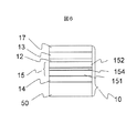
図6に、本発明の代表的なセンサユニットの磁気抵抗効果積層膜10の構成を示す。基体50上に、下地膜14、第一の強磁性膜151、反平行結合層154、第二の強磁性膜152、非磁性中間層12、軟磁性自由層13、保護膜17を形成してなる。このうち、第一の強磁性膜151と第二の強磁性膜152は、反平行結合層154を介して反強磁性的に強く結合し、互いの磁化が反平行な状態になるよう形成される。この部分は外部からの磁界に対してその磁化方向が実質的に固定されてなり、強磁性固定層15として機能する。外部からの磁界に対して、磁化方向が変わらない強磁性固定層15と、外部からの磁界に対して良好に磁化方向を回転させる軟磁性自由層13の相対的な磁化方向の角度差に応じて、非磁性中間層12を介した導電度が変わることで磁気抵抗効果が発生し、信号出力が得られる。すなわち、各センサユニットの感知すべき磁界方向に対する角度の基準は、上記強磁性固定層15の固定された磁化の方向によって決定される。
FIG. 6 shows a configuration of a magnetoresistive
次に、本発明のセンサユニットの磁気抵抗効果積層膜のより詳細な構成について述べる。 Next, a more detailed configuration of the magnetoresistive laminated film of the sensor unit of the present invention will be described.
図7は、下地膜上に形成したCo−Fe膜の保磁力とFe組成の関係について示した図である。Co−Fe膜の組成に対して、Co−Fe膜の保磁力は大きく変化することがわかる。Fe組成が40at%より小さい領域では、Co−Fe膜の保磁力は4kA/m(50Oe)以下と小さく、比較的容易に磁化が回転することがわかる。一方、Fe組成が40〜80at%(Fe−20〜60at%Co)では、保磁力は8kA/m(100Oe)以上と大きくなり、磁化の回転に対して強くなることがわかる。そこで、本発明の角度センサのセンサユニットは、第一の強磁性膜として、Fe−20〜60at%Co薄膜を用いるとよい。これにより、本発明の角度センサに用いるセンサユニットでは、外部磁界に対して高い安定性を示すとともに、方向性を決定する着磁の容易性や、高い出力の実現が可能になる。第二の強磁性膜としては、Co−0〜40at%Fe薄膜を用いるとよい。 FIG. 7 is a diagram showing the relationship between the coercive force and the Fe composition of the Co—Fe film formed on the base film. It can be seen that the coercivity of the Co—Fe film varies greatly with respect to the composition of the Co—Fe film. In the region where the Fe composition is less than 40 at%, the coercive force of the Co—Fe film is as small as 4 kA / m (50 Oe) or less, and it can be seen that the magnetization rotates relatively easily. On the other hand, it can be seen that when the Fe composition is 40 to 80 at% (Fe-20 to 60 at% Co), the coercive force is as large as 8 kA / m (100 Oe) or more and is strong against the rotation of magnetization. Therefore, the sensor unit of the angle sensor of the present invention may use an Fe-20 to 60 at% Co thin film as the first ferromagnetic film. Thereby, in the sensor unit used for the angle sensor of the present invention, it is possible to realize high stability with respect to an external magnetic field, easy magnetization for determining directionality, and high output. As the second ferromagnetic film, a Co-0 to 40 at% Fe thin film may be used.
図7から見て取れるように、このような組成にすることによって、第二の強磁性膜の保磁力を第一の強磁性膜に比べて小さい値に保つことができ、結果的に強磁性固定層の磁気的な安定度を高くできる。第一の強磁性膜の保磁力に対して、第二の強磁性膜の保磁力を小さくすることは、互いに反平行結合層を介して強く反強磁性的に結合したこれらの強磁性膜において、保磁力の大きい第一の強磁性膜の磁化方向が優先される機能を発揮させ、しいては強磁性固定層の磁化状態の安定性を高くできる。また、第二の強磁性膜は、構造上中間層に直接隣接して磁気抵抗効果を発揮する機能を担うので、組成決定には高い磁気抵抗効果が得られるような組成を選ぶこともでき、特にCo−10at%Fe薄膜を用いると高い磁化の安定性と高い抵抗変化率を両立できる。 As can be seen from FIG. 7, with such a composition, the coercive force of the second ferromagnetic film can be kept smaller than that of the first ferromagnetic film, resulting in a ferromagnetic fixed layer. Can increase the magnetic stability. Reducing the coercivity of the second ferromagnetic film relative to the coercivity of the first ferromagnetic film means that these ferromagnetic films are strongly antiferromagnetically coupled to each other via antiparallel coupling layers. The function of giving priority to the magnetization direction of the first ferromagnetic film having a large coercive force can be exhibited, and the stability of the magnetization state of the ferromagnetic pinned layer can be increased. In addition, since the second ferromagnetic film bears a function of exerting a magnetoresistive effect directly adjacent to the intermediate layer in structure, a composition that can obtain a high magnetoresistive effect can be selected for determining the composition. In particular, when a Co-10 at% Fe thin film is used, both high magnetization stability and a high resistance change rate can be achieved.
図8は、磁気抵抗効果のCo−Fe組成の依存性を示す参考データである。データは以下の構造の膜についての実験結果である。基体/下地膜/MnPt/Co−10at%Fe膜/Ru/Co−10at%Fe膜/Co−Fex膜/Cu/Co−10at%Fe/Ni−20%Fe膜/保護膜。本発明のセルフピン型スピンバルブと同一ではないが、巨大磁気抵抗の発生機構は同じなので、Co−Fe強磁性膜の組成に関する知見として参考にすることができる。 FIG. 8 is reference data showing the dependence of the magnetoresistive effect on the Co—Fe composition. Data are experimental results for films of the following structure. Substrate / underlayer / MnPt / Co-10at% Fe film / Ru / Co-10at% Fe film / Co-Fe x film / Cu / Co-10at% Fe / Ni-20% Fe film / protection film. Although it is not the same as the self-pin type spin valve of the present invention, the mechanism of generation of giant magnetoresistance is the same, so that it can be referred as knowledge relating to the composition of the Co—Fe ferromagnetic film.
図8から、Co−Fex部の組成を変えると、Fe組成の増大に伴ってMR比は徐々に低下していることがわかる。Fe組成を30at%以上にするとCo−Fe合金のfcc/bcc構造境界に相当するが、この組成領域でMR比は大きく低下していることがわかる。これはCo−Fe薄膜がbcc構造になると巨大磁気抵抗効果を生じる他の層、すなわちCu非磁性中間層やCoFe/NiFe軟磁性自由層のfcc構造の層と結晶学的な不一致を生じ、これが電子の散乱要因となって磁気抵抗を低下させるものと思われる。Feをさらに増やしていくとMR比はさらに低下しているが、これはFe/Cuの組み合わせがCo/Cuの組み合わせより巨大磁気抵抗効果が小さいことは学術論文などで報告がある現象と同様と考えられる。このような理由から本発明の第二の強磁性膜には、Co−Fe薄膜でFe組成が40at%以下の範囲であって、さらに、20at%以下、特に10at%程度とすることが望ましい。 8, changing the composition of Co-Fe x unit, MR ratio with increasing Fe composition gradually seen to decrease. When the Fe composition is 30 at% or more, it corresponds to the fcc / bcc structure boundary of the Co—Fe alloy, but it can be seen that the MR ratio is greatly reduced in this composition region. This causes crystallographic inconsistencies with other layers that produce a giant magnetoresistive effect when the Co-Fe thin film has a bcc structure, that is, a fcc structure layer of a Cu nonmagnetic intermediate layer or a CoFe / NiFe soft magnetic free layer. It seems to be a factor of electron scattering and reduce the magnetic resistance. As the Fe content is further increased, the MR ratio is further decreased, but this is similar to the phenomenon reported in academic papers, etc., that the Fe / Cu combination has a smaller giant magnetoresistance effect than the Co / Cu combination. Conceivable. For these reasons, it is desirable that the second ferromagnetic film of the present invention has a Co-Fe thin film with an Fe composition of 40 at% or less, more preferably 20 at% or less, particularly about 10 at%.
本発明のセンサユニット用磁気抵抗効果膜で、このような組成の第一の強磁性膜及び第二の強磁性膜を用いることの別の理由は、本発明の角度センサの目的である広い温度領域で動作可能、という機能を達成するための温度依存性という物性がある。一般に言って、強磁性体の磁化は温度の上昇による熱揺らぎによって減少していき、その温度特性は、その物質のキュリー温度によって決まる。よく知られているようにFeのキュリー温度は770℃、Coは1120℃、Niは358℃である。仮に、セルフピン型の強磁性固定層を、それぞれFeとCoの層で作製した場合、室温での飽和磁束密度はそれぞれおよそ2.1T、1.6Tであるから、互いの磁化量の差分がゼロになるようにFe層の厚さとCo層の厚さを1.6:2.1に設定すれば、およそ磁化量の差分をゼロにできる。しかしながら、FeとCoではキュリー温度が違うので、温度の上昇とともに、それぞれの磁化の量はブリルアン関数的に低下していき、その結果、磁化の磁化量の差分は次第にゼロからずれていく。 Another reason for using the first ferromagnetic film and the second ferromagnetic film having such a composition in the magnetoresistive film for the sensor unit of the present invention is the wide temperature that is the object of the angle sensor of the present invention. There is a physical property of temperature dependence to achieve the function of being operable in the region. Generally speaking, the magnetization of a ferromagnet decreases due to thermal fluctuation due to temperature rise, and its temperature characteristics are determined by the Curie temperature of the material. As is well known, the Curie temperature of Fe is 770 ° C., Co is 1120 ° C., and Ni is 358 ° C. If the self-pinned ferromagnetic pinned layer is made of Fe and Co layers, respectively, the saturation magnetic flux densities at room temperature are approximately 2.1T and 1.6T, respectively. If the thickness of the Fe layer and the thickness of the Co layer are set to 1.6: 2.1 so that, the difference in the amount of magnetization can be made approximately zero. However, since the Curie temperature differs between Fe and Co, the amount of magnetization decreases with a Brillouin function as the temperature rises, and as a result, the difference in magnetization amount of magnetization gradually deviates from zero.
図9に、磁化量の温度依存性を概念的に示した図を示す。図9(a)はキュリー温度の異なる強磁性膜を用いたセルフピン型強磁性固定層の特性を示した図、図9(b)はキュリー温度の同等な強磁性膜を用いたセルフピン型強磁性固定層の特性を示した図である。 FIG. 9 is a diagram conceptually showing the temperature dependence of the magnetization amount. FIG. 9A shows the characteristics of a self-pinned ferromagnetic pinned layer using ferromagnetic films having different Curie temperatures, and FIG. 9B shows a self-pinned ferromagnetic film using ferromagnetic films having the same Curie temperature. It is the figure which showed the characteristic of the fixed layer.
キュリー温度の異なる強磁性膜を用いた場合、8(a)に示すように、キュリー温度の違いにより、200℃での磁化量の差分ΔMはゼロからのずれが増加し、このため、強磁性固定層は外部磁界に対して不安定になる。この現象は、特許文献3において加熱又は冷却による強磁性固定層の着磁に利用されるのと同じ原理であるが、本発明の主旨は、この現象を逆に抑制した構造を採用することによって、温度の上昇に対して安定な角度センサを供給することにあるのである。R. M. Bozorth, “Ferromagnetism” (D. Van Nostrand Co. Inc., N. Y., (1951)によれば、Fe40Co60は980℃付近に相変態点があり磁性を失うが、低温側から外挿される“virtual”な、実質的なキュリー温度はおよそ1140℃である。この温度はCoのキュリー温度1120℃に極めて近い。このような物性は、CoとFe40Co60が実質的にほぼ同程度の磁化の温度依存性を持つことを示している。これら2つの組成は上述した本発明の第一および第二の強磁性膜の近く、したがって本発明の第一および第二の強磁性膜はその合金組成からともに1100℃付近の同程度のキュリー温度を持ち、温度の上昇に対して類似の磁化の温度依存性をもつことが期待できる。一方、図9(b)は、本発明のセンサユニット用磁気抵抗効果膜の強磁性固定層の磁化の温度特性の概念図を示している。強磁性固定層をキュリー温度の同等な材料から構成することにより、広い温度領域においてΔMがゼロ近傍であるセンサユニット用磁気抵抗効果膜を得ることができ、低温から高温まで安定に動作する角度センサを実現できる。
When ferromagnetic films having different Curie temperatures are used, as shown in FIG. 8 (a), the difference ΔM in the amount of magnetization at 200 ° C. increases from zero due to the difference in Curie temperature. The fixed layer becomes unstable against an external magnetic field. This phenomenon is the same principle as that used in the magnetization of the ferromagnetic fixed layer by heating or cooling in
図10に、強磁性固定層に反平行結合層としてRuを用いたときの残留磁化の量Mrと、磁界160kA/m(20kOe)での磁化量M160を示した。残留磁化の量Mrは、Ru反平行結合層の厚さが0.6nm近傍で大きくなっており、Ruの厚さが0.3〜0.45nm、及び0.7〜1nmではほぼゼロになっている。これはRuの厚さによって、強磁性固定層を構成する第一の強磁性層と第二の強磁性膜の間の反強磁性的結合力が変化することを示している。すなわち、Ru反平行結合層の厚さが0.3〜0.45nm、及び0.7〜1nmの時には、反強磁性的結合は良好であるが、Ru反平行結合層の厚さが0.6nm近傍では強磁性的であって、このため残留磁化成分が増加しているのである。次に、印加磁界160kA/m(20kOe)での磁化の量であるM160についてみると、Ru反平行結合層の厚さが0.45nm以下に薄くなると減少していることがわかる。これは、Ru反平行結合層の厚さが0.45nm以下では強磁性固定層が外部磁界160kA/m(20kOe)で飽和しないほど反強磁性結合が強くなっていることを意味する。結果、Ru反強磁性層の厚さが0.35nm、もしくはその近傍で0.3〜0.4nmのときが強磁性固定層の反強磁性的結合がもっとも強く、残留磁化成分もほぼゼロであった。したがって、Ruを反平行結合層に用いる場合、好ましくは0.3〜0.4nmの厚さにすればよいことがわかる。 FIG. 10 shows the amount of residual magnetization Mr when Ru is used as the antiparallel coupling layer in the ferromagnetic pinned layer, and the amount of magnetization M 160 at a magnetic field of 160 kA / m (20 kOe). The amount of residual magnetization Mr increases when the thickness of the Ru antiparallel coupling layer is near 0.6 nm, and becomes almost zero when the thickness of Ru is 0.3 to 0.45 nm and 0.7 to 1 nm. ing. This indicates that the antiferromagnetic coupling force between the first ferromagnetic layer and the second ferromagnetic film constituting the ferromagnetic fixed layer changes depending on the thickness of Ru. That is, when the thickness of the Ru antiparallel coupling layer is 0.3 to 0.45 nm and 0.7 to 1 nm, the antiferromagnetic coupling is good, but the thickness of the Ru antiparallel coupling layer is 0.1. In the vicinity of 6 nm, it is ferromagnetic and therefore the remanent magnetization component is increased. Next, regarding M 160 which is the amount of magnetization in an applied magnetic field of 160 kA / m (20 kOe), it can be seen that it decreases as the thickness of the Ru antiparallel coupling layer is reduced to 0.45 nm or less. This means that when the thickness of the Ru antiparallel coupling layer is 0.45 nm or less, the antiferromagnetic coupling becomes so strong that the ferromagnetic pinned layer is not saturated with an external magnetic field of 160 kA / m (20 kOe). As a result, when the thickness of the Ru antiferromagnetic layer is 0.35 nm or in the vicinity of 0.3 to 0.4 nm, the antiferromagnetic coupling of the ferromagnetic pinned layer is strongest and the residual magnetization component is almost zero. there were. Therefore, it can be seen that when Ru is used for the antiparallel coupling layer, the thickness is preferably 0.3 to 0.4 nm.
図11に、第二の強磁性膜と第一の強磁性膜の磁化量の差ΔMを、第一の強磁性膜の厚さに対して示した。ここで第二の強磁性膜の厚さは一定として、磁化量は飽和磁化(テスラ)×厚さ(ナノメートル)として示した。膜の構成は基体/下地膜/第一の強磁性膜Co−60at%Fe膜/Ru膜/Co−10at%Fe膜(2nm)/Cu/Co−10at%Fe膜/Ni−20at%Fe膜/保護膜とした。第一の強磁性膜の厚さに対して、磁化量の差ΔMは単純に減少し、一定の第二の強磁性膜の厚さに対して適切な第一の強磁性膜の厚さを選択することで磁化量の差ΔMをゼロもしくはその近傍の値に設定することができることがわかる。本発明において、この磁化量の差ΔMは角度センサとしての機能に大きな影響を与える因子である。 FIG. 11 shows the difference ΔM in the magnetization amount between the second ferromagnetic film and the first ferromagnetic film with respect to the thickness of the first ferromagnetic film. Here, the thickness of the second ferromagnetic film is assumed to be constant, and the magnetization amount is shown as saturation magnetization (Tesla) × thickness (nanometer). The structure of the film is substrate / underlayer film / first ferromagnetic film Co-60 at% Fe film / Ru film / Co-10 at% Fe film (2 nm) / Cu / Co-10 at% Fe film / Ni-20 at% Fe film / Protective film. The difference ΔM in the amount of magnetization simply decreases with respect to the thickness of the first ferromagnetic film, and the appropriate thickness of the first ferromagnetic film with respect to the constant thickness of the second ferromagnetic film is reduced. It can be seen that the difference ΔM in the magnetization amount can be set to zero or a value in the vicinity thereof by selecting. In the present invention, this magnetization amount difference ΔM is a factor that greatly affects the function of the angle sensor.
図12に、磁化量の差ΔMを変えたときのセンサユニット用磁気抵抗効果膜の抵抗変化率と最大印加磁界の関係を示した。測定は、磁気抵抗効果膜の強磁性固定層の着磁方向に平行な膜面内方向に磁界を正負に印加して磁気抵抗効果曲線を測定し、最大印加磁界を最初は50A/mとして、順次大きくして行った。これはすなわち、セルフピン型の磁気抵抗効果膜からなるセンサユニットについて、強磁性固定層が外部磁界に対して安定である上限を計測する実験である。 FIG. 12 shows the relationship between the resistance change rate of the magnetoresistive film for sensor unit and the maximum applied magnetic field when the magnetization amount difference ΔM is changed. In the measurement, a magnetoresistive effect curve was measured by applying a magnetic field positively and negatively in the in-plane direction parallel to the magnetization direction of the ferromagnetic pinned layer of the magnetoresistive effect film, and the maximum applied magnetic field was initially set to 50 A / m. It was made larger gradually. This is an experiment for measuring the upper limit at which the ferromagnetic pinned layer is stable against an external magnetic field for a sensor unit made of a self-pin type magnetoresistive film.
磁化量の差ΔMが−0.1〜0.06(nm・T)では、最大印加磁界が160A/m(2000Oe)を越えても高いMR比を保ち続けているが、磁化量の差ΔMが−0.17になると、最大印加磁界160A/m(2000Oe)でのMR比は10%となり、1%程度のMR比の低下が発生していることがわかる。さらに磁化量の差ΔMが−0.24では最大印加磁界160kA/m(2000Oe)でのMR比は8.5%とさらに低下が認められる。このMR比の低下は最大印加磁界をかけた後、より低い磁界で測定しなおしても元の値には復帰しない。これは、磁化量の差ΔMを適切にゼロ近傍にしないと外部磁界によって強磁性固定層の磁化方向が変化して、所定の性能を維持できないことを意味している。 When the magnetization amount difference ΔM is −0.1 to 0.06 (nm · T), the high MR ratio is maintained even when the maximum applied magnetic field exceeds 160 A / m (2000 Oe), but the magnetization amount difference ΔM. When -0.17, the MR ratio at the maximum applied magnetic field of 160 A / m (2000 Oe) is 10%, indicating that the MR ratio is reduced by about 1%. Further, when the difference ΔM in the amount of magnetization is −0.24, the MR ratio at a maximum applied magnetic field of 160 kA / m (2000 Oe) is further decreased to 8.5%. This reduction in MR ratio does not return to the original value even if the measurement is performed again with a lower magnetic field after applying the maximum applied magnetic field. This means that the magnetization direction of the ferromagnetic fixed layer is changed by the external magnetic field unless the difference ΔM in the magnetization amount is appropriately close to zero, and the predetermined performance cannot be maintained.
図13には、センサユニット用磁気抵抗効果膜の電気抵抗の磁界角度依存性を示した。測定は、図13の左の模式図のように、磁気抵抗効果膜の強磁性固定層の着磁方向に対して、面内の角度θで8kA/m(100Oe)の磁界を印加し、角度θを変えた時の抵抗を測定したものである。この抵抗の磁界角度依存性は、本発明のセンサユニット用磁気抵抗効果膜が角度センサとして有効であることを端的に示す。すなわち、角度θを変えると、磁界の方向に磁化が回転する軟磁性自由層と、着磁方向から磁化が変化しない強磁性固定層との磁化のなす角度が変化し、それに応じて磁気抵抗効果が発生する。同時に、このような測定を行うことで、センサユニットを構成する磁気抵抗効果膜の強磁性固定層の着磁の方向を測定することができる。 FIG. 13 shows the magnetic field angle dependence of the electrical resistance of the magnetoresistive film for the sensor unit. As shown in the schematic diagram on the left of FIG. 13, the measurement is performed by applying a magnetic field of 8 kA / m (100 Oe) at an in-plane angle θ with respect to the magnetization direction of the ferromagnetic pinned layer of the magnetoresistive effect film. This is a measurement of resistance when θ is changed. This dependence of the resistance on the magnetic field angle clearly indicates that the magnetoresistive film for a sensor unit of the present invention is effective as an angle sensor. That is, when the angle θ is changed, the angle between the soft magnetic free layer whose magnetization rotates in the direction of the magnetic field and the ferromagnetic pinned layer whose magnetization does not change from the magnetization direction changes, and the magnetoresistive effect accordingly Will occur. At the same time, by performing such a measurement, it is possible to measure the magnetization direction of the ferromagnetic fixed layer of the magnetoresistive effect film constituting the sensor unit.
図14に、磁化量の差ΔMを変えたときのセンサユニット用磁気抵抗効果膜の強磁性固定層の磁化方向ずれと最大印加磁界の関係を示した。磁化量の差ΔMがゼロ近傍では磁化方向ずれはきわめて小さい。磁化量の差ΔMがゼロからずれると、磁化方向ずれは2次関数状の増加が見られ、磁化方向ずれは1°を超えた。 FIG. 14 shows the relationship between the magnetization direction shift of the ferromagnetic fixed layer of the magnetoresistive effect film for sensor unit and the maximum applied magnetic field when the difference in magnetization amount ΔM is changed. When the magnetization amount difference ΔM is near zero, the magnetization direction deviation is extremely small. When the magnetization amount difference ΔM deviated from zero, the magnetization direction deviation increased in a quadratic function, and the magnetization direction deviation exceeded 1 °.
図14に示した角度ずれは、本発明の目的である角度センサ及び角度検出装置において、重大な意味を持つ。特許文献5のような磁気ヘッドへの応用の場合、図12に示したMR比の低下は単純に信号出力が低下するのであって、多少のMR比の低下はデメリットではあるが致命的ではない。さらに、磁気ヘッドの場合に図14のような数度以下の角度ずれは、実質的に磁気ヘッドの性能に影響しない。これに対して本発明の角度センサでは、検出すべき角度はこの角度ずれの影響を直接受け、角度ずれが直接角度誤差になってしまう。
The angle deviation shown in FIG. 14 has a significant meaning in the angle sensor and the angle detection device which are the objects of the present invention. In the case of application to a magnetic head as in
図15に、磁化量の差ΔMと、175kA/m(2.2kOe)印加後の強磁性固定層の磁化方向ずれの関係をまとめて示した。磁化量の差ΔMがゼロからずれると、角度ずれは2次関数状の増加が見られ、最小二乗法によって求めた2次関数近似曲線によると、ΔMが負でその絶対値が0.15nm・Tより大きいと、角度ずれは1°を超えた。角度誤差を1°以下とすることが角度センサとしての一定の性能であると考えると、図15から磁化量の差ΔMは−0.15〜0.08とすることで、角度センサとしての必要を満たすことがわかる。以上のように、本発明の角度センサのセンサユニットを反強磁性的に強く結合したFeCo及びCoFe磁性層からなるセルフピン型強磁性固定層を有し、かつ、磁化量の差ΔMを−0.15〜0.08のゼロ近傍に設定することで高い出力と高い安定性を得ることができる。 FIG. 15 collectively shows the relationship between the magnetization amount difference ΔM and the magnetization direction shift of the ferromagnetic fixed layer after application of 175 kA / m (2.2 kOe). When the difference ΔM in magnetization amount deviates from zero, the angle deviation increases in a quadratic function. According to the quadratic function approximation curve obtained by the least square method, ΔM is negative and its absolute value is 0.15 nm · Above T, the angular deviation exceeded 1 °. Considering that the angle error of 1 ° or less is a constant performance as an angle sensor, it is necessary as an angle sensor by setting the difference ΔM in magnetization amount to −0.15 to 0.08 from FIG. You can see that As described above, the sensor unit of the angle sensor of the present invention has the self-pinned ferromagnetic fixed layer composed of the FeCo and CoFe magnetic layers strongly coupled antiferromagnetically, and the difference in magnetization ΔM is −0. High output and high stability can be obtained by setting the value in the vicinity of zero of 15 to 0.08.
図16に、本発明のセンサユニット用磁気抵抗効果膜のMR比の温度依存性を示す。比較のため、よく知られている反強磁性膜を用いたスピンバルブ膜についても示した。通常のスピンバルブ膜では、MR比が−40℃〜150℃まで連続的に低下していく。角度センサの動作温度範囲は絶対的に決まるものではないが、ここでは一般的な角度センサの動作温度として−40℃から150℃とした。上記のような連続な低下は単純に温度の上昇に伴って金属の電気抵抗が増加し、その結果、磁気抵抗効果が低減していると考えられる。本発明の角度センサ用の磁気抵抗効果膜においても同様の傾向を示すことを190℃まで確認できたが、温度の上昇によってMR比が低下する割合に着目すると、本発明のセンサユニット用磁気抵抗効果膜の温度係数は−0.02%/℃、従来のスピンバルブ膜では−0.04%/℃となり、本発明のセンサユニット用磁気抵抗効果膜は温度に対する変化が小さいというメリットがあることがわかる。具体的には−40℃から150℃という動作温度範囲内において、本発明のセンサユニットは従来の構造のセンサに比べて1/3から1/2程度の温度依存性の低減された特性を示すのである。 FIG. 16 shows the temperature dependence of the MR ratio of the magnetoresistive film for sensor unit of the present invention. For comparison, a spin valve film using a well-known antiferromagnetic film is also shown. In a normal spin valve film, the MR ratio continuously decreases from −40 ° C. to 150 ° C. The operating temperature range of the angle sensor is not absolutely determined, but here, the operating temperature of a general angle sensor is set to −40 ° C. to 150 ° C. It is considered that the continuous decrease as described above simply increases the electrical resistance of the metal as the temperature rises, and as a result, the magnetoresistance effect is reduced. It was confirmed that the magnetoresistive effect film for the angle sensor of the present invention showed the same tendency up to 190 ° C. However, when attention is paid to the rate at which the MR ratio decreases with increasing temperature, the magnetoresistive for sensor unit of the present invention The temperature coefficient of the effect film is −0.02% / ° C., and the conventional spin valve film is −0.04% / ° C. The magnetoresistive effect film for the sensor unit of the present invention has the merit that the change with respect to temperature is small. I understand. Specifically, in the operating temperature range of −40 ° C. to 150 ° C., the sensor unit of the present invention exhibits a characteristic in which the temperature dependency is reduced by about 1/3 to 1/2 as compared with a sensor having a conventional structure. It is.
図17に、本発明の角度センサ上に90°ごとに磁場印加方向を変えて薄膜形成した4つのセンサユニットの最大印加磁界と強磁性固定層の磁化の方向の関係を示した。図の縦軸は、各センサの大まかな挙動を見るために、大きな角度範囲に設定されている。ここでは、4つのセンサユニットの各々の強磁性固定層の強磁性膜間の磁化量の差ΔMはほぼゼロに形成した。センサユニット用磁気抵抗効果膜の強磁性固定層を所定の方向の磁界中で形成することで、センサユニット1〜4の強磁性固定層の磁化の方向は、それぞれ0゜、90゜、−180゜、−90°の方向に着磁されており、その方向性は135kA/m(1700Oe)の磁界を印加しても変わっていないことがわかる。このように、本発明のセンサユニットは、磁気抵抗効果膜の形成時の磁界印加方向で着磁方向を決定でき、外部磁界に対して安定であるので、この着磁方向に応じたそれぞれ角度の異なる磁界方向の感知ユニットとして機能する。
FIG. 17 shows the relationship between the maximum applied magnetic field and the magnetization direction of the ferromagnetic pinned layer of four sensor units in which thin films are formed by changing the magnetic field application direction every 90 ° on the angle sensor of the present invention. The vertical axis in the figure is set to a large angle range in order to see the rough behavior of each sensor. Here, the difference ΔM in the amount of magnetization between the ferromagnetic films of the ferromagnetic fixed layers of the four sensor units is formed to be almost zero. By forming the ferromagnetic pinned layer of the magnetoresistive effect film for the sensor unit in a magnetic field in a predetermined direction, the magnetization directions of the ferromagnetic pinned layers of the
上述のように、センサユニットの磁気抵抗効果膜の形成時に磁界を適切な方向に印加することで、強磁性固定層の着磁されたセンサユニットを得ることができる。以下、軟磁性自由層の磁気異方性について述べる。強磁性固定層を磁界を印加して形成すると着磁方向を決定できるが、一方、軟磁性自由層の形成時には、その磁化の方向が容易磁化方向となる一軸異方性が発生する。最も理解しやすい製造方法は、強磁性固定層の磁界印加方向と同一方向に軟磁性自由層の形成時に磁界が印加され、異方性が誘導される場合である。 As described above, by applying a magnetic field in an appropriate direction when the magnetoresistive film of the sensor unit is formed, a sensor unit with a ferromagnetic pinned layer magnetized can be obtained. Hereinafter, the magnetic anisotropy of the soft magnetic free layer will be described. When the ferromagnetic pinned layer is formed by applying a magnetic field, the magnetization direction can be determined. On the other hand, when the soft magnetic free layer is formed, uniaxial anisotropy occurs in which the magnetization direction becomes the easy magnetization direction. The most easily understood manufacturing method is a case where anisotropy is induced by applying a magnetic field when the soft magnetic free layer is formed in the same direction as the magnetic field application direction of the ferromagnetic pinned layer.
図18に、軟磁性自由層の容易磁化方向が強磁性固定層と同一方向であるセンサユニット4個を有する角度センサの角度ずれを示した。ここで角度ずれは、測定磁界の印加方向に対して角度センサの出力から算出された角度とのずれである。図中、点線の測定は0°〜360°への測定、実線は逆に360°〜0°への測定である。両者の間に大きなずれはなく、この角度センサのヒステリシスが大きくないことがわかるが、一方、角度ずれは磁界の印加角度によって変化し、360°測定したときのピークからピークの幅で1.4°もの角度ずれを生じていることがわかる。この角度ずれ発生の原因は、上記結果を4個のセンサユニットのうち、X成分とY成分に分離して測定すると理解しやすい。すなわち、センサユニットのうち、強磁性固定層の着磁方向が0°と180°の一対と、90°と−90°の一対によるハーフブリッジがX成分とY成分に対応する。 FIG. 18 shows the angular deviation of an angle sensor having four sensor units in which the easy magnetization direction of the soft magnetic free layer is the same as that of the ferromagnetic pinned layer. Here, the angle deviation is a deviation from the angle calculated from the output of the angle sensor with respect to the application direction of the measurement magnetic field. In the figure, the dotted line is measured from 0 ° to 360 °, and the solid line is measured from 360 ° to 0 °. There is no large deviation between the two, and it can be seen that the hysteresis of this angle sensor is not great. On the other hand, the angular deviation changes depending on the applied angle of the magnetic field, and the peak-to-peak width when measured at 360 ° is 1.4. It can be seen that there is an angle shift of °. The cause of this angular deviation can be easily understood by measuring the above results separately for the X and Y components of the four sensor units. That is, in the sensor unit, a half bridge formed by a pair of magnetization directions of the ferromagnetic pinned layer of 0 ° and 180 ° and a pair of 90 ° and −90 ° corresponds to the X component and the Y component.
図19は、図18のセンサのX側ユニット及びY側ユニットの出力誤差である。線が各2本あるのは図18と同様に角度の増加方向と減少方向の測定結果であるが、それぞれに大差ないので以降では触れない。ここで出力誤差は、XあるいはY成分のブリッジの出力の最大値と最小値に対応する振幅をもつ測定磁界の印加方向のコサインに対する値のずれを振幅に対して示したものである。X成分、Y成分ともに、磁界印加角度に対して出力誤差は複雑な挙動を示しているが、0〜360°の間に山と谷を2つずつ有する2回成分が特に大きいことがわかる。この時の出力誤差は360°測定した場合のピークからピークで約1.0%であった。 FIG. 19 shows output errors of the X side unit and Y side unit of the sensor of FIG. Although there are two lines each in the same way as in FIG. 18, the measurement results in the increasing direction and decreasing direction are the same. Here, the output error indicates the deviation of the value relative to the cosine in the application direction of the measurement magnetic field having the amplitude corresponding to the maximum value and the minimum value of the output of the X or Y component bridge. Although both the X component and the Y component have a complicated output error with respect to the magnetic field application angle, it can be seen that the two-time component having two peaks and valleys between 0 and 360 ° is particularly large. The output error at this time was about 1.0% from peak to peak when measured at 360 °.
このような出力誤差の発生原因を明確にするため、角度センサの静磁界磁化挙動解析を行った。解析には、4つのセンサユニットの着磁角度、電気抵抗、抵抗変化率に加えて、各々の層間結合磁界、一軸異方性定数を含めた。ここで層間結合磁界は強磁性固定層と軟磁性自由層との磁気的な結合磁界で、作製したセンサユニット用磁気抵抗効果膜の実測値を用いた。一軸異方性定数は、薄膜では測定が困難なので、通常、十分の数A/m(数Oe)程度であることから測定結果とフィッティングすることで求めた。また、X側のセンサユニットとY側のセンサユニットとの間に強磁性固定層の角度設定ずれを仮定し、これもフィッティングパラメーターとした。 In order to clarify the cause of such output error, static magnetic field magnetization behavior analysis of the angle sensor was performed. The analysis included the interlayer coupling magnetic field and uniaxial anisotropy constant in addition to the magnetization angle, electrical resistance, and resistance change rate of the four sensor units. Here, the interlayer coupling magnetic field is a magnetic coupling magnetic field between the ferromagnetic pinned layer and the soft magnetic free layer, and an actual measurement value of the produced magnetoresistive film for sensor unit was used. Since the uniaxial anisotropy constant is difficult to measure with a thin film, the uniaxial anisotropy constant is usually about several A / m (several Oe). In addition, it was assumed that there was a shift in the angle of the ferromagnetic pinned layer between the X-side sensor unit and the Y-side sensor unit, and this was also used as a fitting parameter.
図20に、解析モデルによる出力誤差及び角度ずれの磁界印加角度依存性を示した。図中、実線と1点鎖線が図18、図17に示した実測値、それ以外の□、◆マークは解析による計算結果である。使用した一軸異方性磁界Hk(Oe)、層間結合磁界Hint(Oe)、及び角度設定ずれの値を以下に示す。
センサユニット1:Hk 6、Hint 4.42
センサユニット2:Hk 6、Hint 0.54
センサユニット3:Hk 5、Hint 4.42
センサユニット4:Hk 5、Hint 0.54(単位はOe)
角度設定ずれ−0.2°
FIG. 20 shows the magnetic field application angle dependence of the output error and the angle deviation by the analysis model. In the figure, the solid line and the alternate long and short dash line are the actual measurement values shown in FIGS. 18 and 17, and the other □ and ◆ marks are calculation results by analysis. The values of the used uniaxial anisotropic magnetic field H k (Oe), interlayer coupling magnetic field H int (Oe), and angle setting deviation are shown below.
Sensor unit 1:
Sensor unit 2:
Sensor unit 3:
Sensor unit 4:
Angle setting deviation -0.2 °
図20からわかるように、解析モデルによる出力誤差及び角度誤差は、実測値とよく一致しており、角度センサの誤差・ずれの発生原因がなんであるにせよ、本解析モデル内に考慮されていることがわかる。以下、図20に示した解析の結果を初期解析値と呼ぶことにする。 As can be seen from FIG. 20, the output error and the angle error due to the analysis model are in good agreement with the actual measurement values, and are taken into account in the present analysis model regardless of the cause of the error or deviation of the angle sensor. I understand that. Hereinafter, the analysis result shown in FIG. 20 is referred to as an initial analysis value.
図21に、すべてのセンサユニットに対して層間結合磁界Hintをゼロにした場合のX成分ブリッジの出力誤差を示した。出力誤差は微量に変化したが、ピークからピークの出力誤差は1.0%と変化せず、大略初期解析値又は実測値と変わっていないことがわかる。この時の角度誤差は、1.0°であった。 FIG. 21 shows the output error of the X-component bridge when the interlayer coupling magnetic field H int is zero for all sensor units. Although the output error has changed in a minute amount, the peak-to-peak output error does not change to 1.0%, and it is understood that the output error is not substantially changed from the initial analysis value or the actual measurement value. The angle error at this time was 1.0 °.
一方、図22は、Hint及びHkをゼロにした場合のX成分ブリッジの出力誤差と角度センサの角度誤差である。HkをゼロにしたことでX成分ブリッジの出力誤差が明確に小さくなり、ピークとピークの幅で0.3%と初期解析値の1/4程度、すなわち、実測値の1/4程度になった。同様に角度誤差は0.3°とやはり1/4程度に低減された。この残留した0.3°の誤差は、X及びYセンサの角度ずれなどに起因すると考えられる。 On the other hand, FIG. 22 shows the output error of the X component bridge and the angle error of the angle sensor when H int and H k are zero. By making H k zero, the output error of the X component bridge is clearly reduced, and the peak-to-peak width is 0.3%, which is about 1/4 of the initial analysis value, that is, about 1/4 of the actual measurement value. became. Similarly, the angle error was 0.3 °, which was reduced to about ¼. This remaining error of 0.3 ° is considered to be caused by an angle shift of the X and Y sensors.
以上のことから、角度センサの角度誤差を低減するには軟磁性自由層の一軸異方性の低減が有効であることがわかる。図21で示したHintゼロの場合の角度誤差は1.0°、図22のHkをゼロにした場合の角度誤差は0.3°であって、本発明でHkをゼロにする効果は、実験的にピーク幅で角度誤差0.7°の低減にあたることがわかる。すなわち、本発明のHk低減効果を用いない場合、センサの角度誤差はピーク幅で1.0−0.3=0.7°までの低減が限界であって、本発明の適用によって0.7°より小さい角度誤差が実現できる。 From the above, it can be seen that reducing the uniaxial anisotropy of the soft magnetic free layer is effective in reducing the angle error of the angle sensor. The angle error when H int is zero shown in FIG. 21 is 1.0 °, and the angle error when H k is zero in FIG. 22 is 0.3 °. In the present invention, H k is made zero. It can be seen that the effect is experimentally a reduction of the angle error of 0.7 ° in the peak width. That is, the case of not using the H k reduction effect of the present invention, the angle error of the sensor is a limit to reduce to 1.0-0.3 = 0.7 ° in peak width, 0 by application of the present invention. An angle error smaller than 7 ° can be realized.
さらに具体的に、Hkを低減する方法について述べる。軟磁性自由層の一軸異方性は、センサユニット用磁気抵抗効果膜を熱処理することによって薄膜形成後かつ素子形成後に制御することができる。一般のスピンバルブ膜を含め、極薄い軟磁性自由層の一軸異方性は200℃以上の熱処理を行うと、磁界の方向、又は軟磁性自由層の磁化方向に容易磁化方向をもつ一軸異方性へと熱活性化的に移行するからである。すなわち、回転磁界中で角度センサに熱処理を行い、軟磁性自由層の一軸異方性を、いわば等方化することで、図22に示したような角度誤差の低減された角度センサを得ることができる。 More specifically, a method for reducing H k will be described. Uniaxial anisotropy of the soft magnetic free layer can be controlled after the thin film is formed and after the element is formed by heat-treating the magnetoresistive film for the sensor unit. Uniaxial anisotropy with an easy magnetization direction in the direction of the magnetic field or the direction of magnetization of the soft magnetic free layer when heat treatment at 200 ° C. or higher is carried out, including the general spin valve film. This is because the heat transitions to the sex. That is, by performing heat treatment on the angle sensor in a rotating magnetic field and making the uniaxial anisotropy of the soft magnetic free layer isotropic, the angle sensor with reduced angle error as shown in FIG. 22 is obtained. Can do.
ここで、従来の角度センサで問題となるのは、上記のように軟磁性自由層の一軸異方性を等方化する熱処理を行うと、反強磁性膜の交換結合異方性が低減、等方化、あるいは分散の増加を生じ、角度センサとしての機能を損失することである。一方で、本発明の角度センサでは、ここまで述べてきたように、高温まで外部磁界に対しても安定に動作するセンサユニットを有しており、反強磁性膜の交換結合磁界を応用していない。上記の軟磁性自由層の一軸異方性の等方化熱処理は、本発明の高安定性のセンサユニットにおいてはじめて、極めて有効な手法となるのである。 Here, the problem with the conventional angle sensor is that the exchange coupling anisotropy of the antiferromagnetic film is reduced by performing heat treatment to make the uniaxial anisotropy of the soft magnetic free layer isotropic as described above. This is to cause isotropicity or increase in dispersion and to lose the function as an angle sensor. On the other hand, as described above, the angle sensor of the present invention has a sensor unit that operates stably against an external magnetic field up to a high temperature and applies an exchange coupling magnetic field of an antiferromagnetic film. Absent. The uniaxially anisotropic isotropic heat treatment of the soft magnetic free layer is an extremely effective technique for the first time in the highly stable sensor unit of the present invention.
等方化熱処理は、軟磁性自由層の磁化を所定の方向に磁化するに足りる程度の磁界を印加して、基体の面内方向に回転しながら熱処理及び冷却することによって、一軸異方性の方向性を均質化することで達成できる。熱処理中に近辺の強磁性材料の機材からの磁界や地磁気などの影響を受けないように、回転熱処理中及び冷却時に適切な大きさの磁界、4〜40kA/m(50〜500Oe)程度の磁界を回転して加えることで、軟磁性自由層の磁化方向を時間的に均等化できる。この適切な磁界の大きさは、磁性膜の誘導磁気異方性及び帯状にパターニングしたことによる形状異方性磁界より大きく、図14に示したような強磁性固定層のずれを高温においても生じないように、選択する必要がある。この適切な範囲を逸脱すると、磁界が低すぎて誘導異方性消失熱処理の効果が十分得られないか、強磁性固定層の着磁方向にずれが生じて出力の低下や角度誤差の増加を起こす恐れがあるからである。適切な磁界におけるこの消失処理により、一軸異方性の方向性を均等化し、本発明の角度センサの角度誤差を低減することができる。 In the isotropic heat treatment, a magnetic field sufficient to magnetize the soft magnetic free layer in a predetermined direction is applied, and the heat treatment and cooling are performed while rotating in the in-plane direction of the substrate, thereby causing uniaxial anisotropy. This can be achieved by homogenizing the directionality. A magnetic field of an appropriate magnitude during rotating heat treatment and during cooling so that it is not affected by magnetic fields or geomagnetism from nearby ferromagnetic materials during heat treatment, and a magnetic field of about 4 to 40 kA / m (50 to 500 Oe). By rotating and adding, the magnetization direction of the soft magnetic free layer can be equalized in time. The appropriate magnitude of the magnetic field is larger than the induced magnetic anisotropy of the magnetic film and the shape anisotropy magnetic field obtained by patterning in a strip shape, and the shift of the ferromagnetic fixed layer as shown in FIG. 14 occurs even at a high temperature. There is no need to choose. Beyond this appropriate range, the magnetic field is too low to achieve the effect of induction anisotropy disappearance heat treatment sufficiently, or the magnetization direction of the ferromagnetic pinned layer is shifted to reduce the output and increase the angle error. Because there is a risk of waking up. By this disappearance process in an appropriate magnetic field, the directionality of uniaxial anisotropy can be equalized and the angle error of the angle sensor of the present invention can be reduced.
上記の方法によってHkを低減した角度センサを作製、測定することによって、本発明の角度センサではピーク幅で0.8°以下の角度誤差を実現できることを確認できた。熱処理の方法については、回転磁界でなく、磁界方向のスイッチング、例えば0°と90°とのスイッチング熱処理でも回転磁界中熱処理と同様の効果を得ることができる。もし、熱処理中の軟磁性自由層の磁化方向が、地磁気などの要因によって特定の方向を向かないのであれば、無磁界中熱処理によって軟磁性自由層の一軸異方性の方向性を低減させることも可能である。ここで無磁界中熱処理としては、外部磁界が実質的に磁性膜の磁化状態を飽和させない範囲であることが必然であるから、一般的な軟磁性といわれる磁性膜の保磁力の大きさより小さい、0.8kA/m(10エルステッド)以下、であるべきである。 By producing and measuring an angle sensor with reduced H k by the above method, it was confirmed that the angle sensor of the present invention can realize an angle error of 0.8 ° or less in peak width. As for the heat treatment method, the same effect as the heat treatment in the rotating magnetic field can be obtained by switching not in the rotating magnetic field but also in switching in the magnetic field direction, for example, switching heat treatment at 0 ° and 90 °. If the magnetization direction of the soft magnetic free layer during heat treatment does not point in a specific direction due to factors such as geomagnetism, the uniaxial anisotropy directionality of the soft magnetic free layer should be reduced by heat treatment in a magnetic field. Is also possible. Here, the heat treatment in a magnetic field is inevitably in a range in which the external magnetic field does not substantially saturate the magnetization state of the magnetic film, and is smaller than the coercive force of the magnetic film, which is generally called soft magnetism. Should be 0.8 kA / m (10 oersted) or less.
等方化熱処理の適切な温度範囲は、一つには軟磁性自由層の誘導異方性(一軸異方性)が熱的に変更可能になる温度であって、およそ200℃より上である。一方、温度の高温側の上限は、本発明の角度センサの耐熱性によって決定される。図23に、本発明のセンサユニットの熱処理後の磁気抵抗効果曲線を示す。熱処理は無磁界中で行い、熱処理時間は3時間とした。図23の左の図には磁気抵抗効果曲線を示したが、熱処理温度310℃まではMR比の低下はなく、320℃ではMR比が低下した。MR比の低下に伴って、磁気抵抗効果曲線はステップ関数的ないわゆるスピンバルブ状の磁気抵抗効果曲線からはずれており、強磁性固定層と軟磁性自由層の間の磁気的な独立が保てなくなった結果と考えられる。図23の右の図には熱処理温度とMR比の関係が示されており、本発明のセンサユニット用磁気抵抗効果膜の熱処理温度としては300℃以下とするとよいことがわかる。200℃以下では誘導磁気異方性が変化しがたいし、300℃を超える温度では、角度センサを構成する磁気抵抗効果膜の特性が低下するからである。 A suitable temperature range for the isotropic heat treatment is, in part, a temperature at which the induced anisotropy (uniaxial anisotropy) of the soft magnetic free layer can be changed thermally, and is above about 200 ° C. . On the other hand, the upper limit on the high temperature side is determined by the heat resistance of the angle sensor of the present invention. FIG. 23 shows a magnetoresistive effect curve after heat treatment of the sensor unit of the present invention. The heat treatment was performed in the absence of a magnetic field, and the heat treatment time was 3 hours. The magnetoresistive effect curve is shown in the left diagram of FIG. 23. The MR ratio did not decrease up to the heat treatment temperature of 310 ° C., and the MR ratio decreased at 320 ° C. As the MR ratio decreases, the magnetoresistive effect curve deviates from the so-called spin valve-like magnetoresistive effect curve in a step function, and magnetic independence between the ferromagnetic pinned layer and the soft magnetic free layer can be maintained. This is probably the result of the loss. 23 shows the relationship between the heat treatment temperature and the MR ratio. It can be seen that the heat treatment temperature of the magnetoresistive film for sensor unit of the present invention should be 300 ° C. or lower. This is because the induced magnetic anisotropy hardly changes at 200 ° C. or less, and the characteristics of the magnetoresistive film constituting the angle sensor deteriorate at a temperature exceeding 300 ° C.
図24に、本発明の角度センサの製造方法のフロー例を示した。8つのセンサユニットを着磁方向の異なる4対から形成する場合、基体上に第一階層のセンサユニットを形成するには、磁気抵抗効果膜の形成を所定の磁界方向で行い、これをパターニングし、絶縁膜で覆う工程を行う。次に第二階層について同様の工程を、ただし、磁気抵抗効果膜の形成時の磁界方向を変えて行う。第三階層及び第四階層についても、同様の工程を行う。電極端子の製造工程については割愛したが、各階層ごとに形成してもよいし、最後の階層を形成後に、第一階層まで電極端子部を貫通する工程と、電極材料を形成する工程を行って形成してもよい。最後に、軟磁性自由層の誘導異方性消失熱処理を行う。 FIG. 24 shows a flow example of the manufacturing method of the angle sensor of the present invention. When the eight sensor units are formed from four pairs having different magnetization directions, in order to form the first level sensor unit on the substrate, the magnetoresistive film is formed in a predetermined magnetic field direction and patterned. Then, a step of covering with an insulating film is performed. Next, the same process is performed for the second layer, except that the direction of the magnetic field when the magnetoresistive film is formed is changed. The same process is performed for the third and fourth layers. Although the manufacturing process of the electrode terminal is omitted, it may be formed for each layer, or after the last layer is formed, the step of penetrating the electrode terminal part to the first layer and the step of forming the electrode material are performed. May be formed. Finally, a heat treatment for eliminating the induced anisotropy of the soft magnetic free layer is performed.
図25に、本発明の角度センサの製造方法の例を工程断面図によって示した。ここでは階層構成を単純化して示すために、図3の左側図に準じた描画を用いた。図24に示したフローの工程を、図25に示したように階層的な構成として作製していく。第一の階層では、図25(a)に示すように、基体50上に磁気抵抗効果膜10の形成を例えば紙面手前方向に磁場を印加して行い、図25(b)に示すように磁気抵抗効果膜をパターニングして第一のセンサユニット511と第四のセンサユニット514を形成する。その後、図25(c)のように絶縁膜41の形成を行う。次に、第二階層の形成を行う。最初に、図25(d)のように、磁気抵抗効果膜10の形成を紙面奥行き方向に磁場を印加して行い、図25(e)のように磁気抵抗効果膜をパターンニングして第二のセンタユニット522と第三のセンサユニット523を形成する。その後、絶縁膜42を形成する。
In FIG. 25, the example of the manufacturing method of the angle sensor of this invention was shown with process sectional drawing. Here, in order to simplify the hierarchical structure, drawing according to the left side of FIG. 3 is used. The steps of the flow shown in FIG. 24 are produced as a hierarchical structure as shown in FIG. In the first hierarchy, as shown in FIG. 25A, the
続いて、図25(f)に示すように、例えば紙面左から右方向に磁場を印加しながら第三層用の磁気抵抗効果膜10を成膜する。次に、図25(g)に示すように、磁気抵抗効果膜をパターンニングして第五のセンタユニット531と第八のセンサユニット534を形成する。その後、絶縁膜43を形成する。次に、図25(h)に示すように、紙面右から左方向に磁場を印加しながら第四層用の磁気抵抗効果膜10を成膜する。次に、図25(i)に示すように、磁気抵抗効果膜をパターンニングして第六のセンタユニット542と第七のセンサユニット543を形成する。その後、絶縁膜44を形成する。
Subsequently, as shown in FIG. 25 (f), for example, the third
このように、第一、第二、第三、第四の階層の磁気抵抗効果膜の形成工程で、図25中に矢印で示すように磁場印加方向を変える。このような作製方法により、複数のセンサユニットが階層ごとに着磁方向が異なるように形成される。その後、誘導異方性消失熱処理を行って軟磁性自由層の誘導異方性を低減し、ブリッジ回路を組むことで、角度誤差の少ない角度センサを得ることができる。 In this way, the magnetic field application direction is changed as shown by the arrows in FIG. 25 in the first, second, third, and fourth layer magnetoresistive film forming steps. By such a manufacturing method, the plurality of sensor units are formed so that the magnetization directions are different for each layer. Thereafter, an induced anisotropy disappearing heat treatment is performed to reduce the induced anisotropy of the soft magnetic free layer, and by building a bridge circuit, an angle sensor with little angle error can be obtained.
図26に、本発明の角度センサを用いた角度検出装置の構成例を示す。回転駆動体63は回転駆動軸62に対して回転運動し、磁石61を角度センサ55に対して相対的に回転運動させる。ここでは上記角度センサが回転軸中に設置され、回転軸の周囲を磁石が回転する回転機構を記載した。この回転運動により、角度センサ55には磁石61から回転角度に応じた方向に磁界が印加され、角度センサ55の出力から回転駆動体63と回転駆動軸62の角度関係を検知できる。
In FIG. 26, the structural example of the angle detection apparatus using the angle sensor of this invention is shown. The
以上のような構成で本発明の角度センサ及び角度検出装置を構成することで、広い温度範囲において出力が大きく、角度ずれが小さい、角度センサ及び角度検出装置を得ることができる。 By configuring the angle sensor and the angle detection device of the present invention with the above-described configuration, it is possible to obtain an angle sensor and an angle detection device that have a large output and a small angle deviation in a wide temperature range.
10 磁気抵抗効果膜
12 非磁性中間層
13 軟磁性自由層
14 下地膜
15 強磁性固定層
151 第一の強磁性膜
152 第二の強磁性膜
154 反平行結合層
17 保護膜
41 絶縁膜
42 絶縁膜
43 絶縁膜
44 絶縁膜
50 基体
501 電極端子
502 磁気抵抗効果膜パターン配線
503 貫通電極端子
511 第一のセンサユニット
522 第二のセンサユニット
523 第三のセンサユニット
514 第四のセンサユニット
531 第五のセンサユニット
542 第六のセンサユニット
543 第七のセンサユニット
534 第八のセンサユニット
55 角度センサ
61 磁石
62 回転駆動軸
63 回転駆動体
DESCRIPTION OF
Claims (16)
各センサユニットは、反平行結合膜を介して第一の強磁性膜と第二の強磁性膜を反強磁性的に結合させてなるセルフピン止め型の強磁性固定層と、非磁性中間層と、軟磁性自由層とを有し、前記第一の強磁性膜と第二の強磁性膜はキュリー温度が略同じかつ磁化量の差が実質的にゼロであり、
異なる階層に属するセンサユニットの強磁性固定層の磁化はそれぞれ異なる方向を向いており、
前記複数のセンサユニットによって外部磁界に応じた信号を出力するブリッジ回路が組まれていることを特徴とする角度センサ。 A plurality of magnetoresistive effect type sensor units have a hierarchical structure laminated in the film thickness direction via an insulating film,
Each sensor unit includes a self-pinned ferromagnetic fixed layer formed by antiferromagnetically coupling a first ferromagnetic film and a second ferromagnetic film via an antiparallel coupling film, a nonmagnetic intermediate layer, A soft magnetic free layer, wherein the first ferromagnetic film and the second ferromagnetic film have substantially the same Curie temperature and the difference in magnetization is substantially zero,
The magnetizations of the ferromagnetic pinned layers of sensor units belonging to different layers are directed in different directions,
An angle sensor, wherein a bridge circuit for outputting a signal corresponding to an external magnetic field is assembled by the plurality of sensor units.
第一階層の絶縁膜を形成する工程と
第二階層のセンサユニットを形成する工程と、
第二階層の絶縁膜を形成する工程と、
第三階層のセンサユニットを形成する工程と、
第三階層の絶縁膜を形成する工程と、
第四階層のセンサユニットを形成する工程と、
第四階層の絶縁膜を形成する工程と、
200℃以上、300℃以下の温度において熱処理する工程とを有し、
各階層のセンサユニットを形成する工程は、第一の強磁性膜を所定の磁界印加中で形成する工程と、前記一の強磁性膜の上に反平行結合層を形成する工程と、前記反平行結合層の上に第二の強磁性膜を形成する工程と、前記第二の強磁性膜の上に非磁性中間層を形成する工程と、前記非磁性中間層の上に軟磁性自由層を形成する工程と、当該センサユニットをパターニングする工程とを含み、
各階層のセンサユニットを形成する工程で印加する磁界の方向が異なり、
前記熱処理は前記軟磁性自由層の誘導異方性消失熱処理である
ことを特徴とする角度センサの製造方法。 Forming a first-tier sensor unit on a substrate;
Forming a first layer insulating film; forming a second layer sensor unit;
Forming a second level insulating film;
Forming a third-tier sensor unit;
Forming a third-layer insulating film;
Forming a fourth level sensor unit;
Forming a fourth level insulating film;
Heat treatment at a temperature of 200 ° C. or higher and 300 ° C. or lower,
The step of forming the sensor unit at each level includes the step of forming the first ferromagnetic film while applying a predetermined magnetic field, the step of forming an antiparallel coupling layer on the one ferromagnetic film, Forming a second ferromagnetic film on the parallel coupling layer; forming a nonmagnetic intermediate layer on the second ferromagnetic film; and a soft magnetic free layer on the nonmagnetic intermediate layer And patterning the sensor unit,
The direction of the magnetic field applied in the process of forming the sensor unit at each level is different.
The method of manufacturing an angle sensor, wherein the heat treatment is an induction anisotropy disappearance heat treatment of the soft magnetic free layer.
前記角度センサに対して相対的に回転運動をする磁石と、
前記角度センサが設置された、回転運動をするための回転軸と、
前記回転軸の周囲を前記磁石が回転する回転機構と、
を備えることを特徴とする角度検知装置。 A plurality of magnetoresistive effect type sensor units have a hierarchical structure in which the film thickness direction is laminated via an insulating film, and each sensor unit has a first ferromagnetic film and a second ferromagnetic film via an antiparallel coupling film. A ferromagnetic fixed layer formed by antiferromagnetically coupling the ferromagnetic films, a nonmagnetic intermediate layer, and a soft magnetic free layer, wherein the first ferromagnetic film and the second ferromagnetic film are Curie The magnetizations of the ferromagnetic pinned layers of the sensor units belonging to the same layer are oriented in the same direction and the magnetizations of the ferromagnetic pinned layers of the sensor units belonging to the different layers are substantially the same and the difference in the amount of magnetization is substantially zero. An angle sensor that is directed in a different direction, and in which a bridge circuit that outputs a signal according to an external magnetic field is assembled by the plurality of sensor units;
A magnet that rotates relative to the angle sensor;
A rotating shaft for rotational movement, wherein the angle sensor is installed;
A rotating mechanism in which the magnet rotates around the rotating shaft;
An angle detection device comprising:
Priority Applications (5)
| Application Number | Priority Date | Filing Date | Title |
|---|---|---|---|
| JP2008019647A JP4780117B2 (en) | 2008-01-30 | 2008-01-30 | Angle sensor, manufacturing method thereof, and angle detection device using the same |
| US12/864,997 US8564282B2 (en) | 2008-01-30 | 2008-12-03 | Angle sensor, angle sensor manufacturing method, and angle detection device using the angle sensor |
| CN200880125816XA CN101932912B (en) | 2008-01-30 | 2008-12-03 | Angle sensor, angle sensor manufacturing method, and angle detection device using the angle sensor |
| EP08871786.3A EP2256463B1 (en) | 2008-01-30 | 2008-12-03 | Angle sensor, angle sensor manufacturing method, and angle detection device using the angle sensor |
| PCT/JP2008/071944 WO2009096093A1 (en) | 2008-01-30 | 2008-12-03 | Angle sensor, angle sensor manufacturing method, and angle detection device using the angle sensor |
Applications Claiming Priority (1)
| Application Number | Priority Date | Filing Date | Title |
|---|---|---|---|
| JP2008019647A JP4780117B2 (en) | 2008-01-30 | 2008-01-30 | Angle sensor, manufacturing method thereof, and angle detection device using the same |
Publications (2)
| Publication Number | Publication Date |
|---|---|
| JP2009180604A JP2009180604A (en) | 2009-08-13 |
| JP4780117B2 true JP4780117B2 (en) | 2011-09-28 |
Family
ID=40912453
Family Applications (1)
| Application Number | Title | Priority Date | Filing Date |
|---|---|---|---|
| JP2008019647A Active JP4780117B2 (en) | 2008-01-30 | 2008-01-30 | Angle sensor, manufacturing method thereof, and angle detection device using the same |
Country Status (5)
| Country | Link |
|---|---|
| US (1) | US8564282B2 (en) |
| EP (1) | EP2256463B1 (en) |
| JP (1) | JP4780117B2 (en) |
| CN (1) | CN101932912B (en) |
| WO (1) | WO2009096093A1 (en) |
Families Citing this family (34)
| Publication number | Priority date | Publication date | Assignee | Title |
|---|---|---|---|---|
| EP2442118B1 (en) | 2009-06-12 | 2021-11-10 | Alps Alpine Co., Ltd. | Magnetic balance current sensor |
| CN102812376B (en) * | 2010-03-12 | 2016-02-10 | 阿尔卑斯电气株式会社 | The magnetic balance type current sensor of magnetic sensor and use magnetic sensor |
| JP5476518B2 (en) | 2010-03-12 | 2014-04-23 | アルプス電気株式会社 | Manufacturing method of magnetic sensor |
| WO2011111494A1 (en) * | 2010-03-12 | 2011-09-15 | アルプス電気株式会社 | Magnetic sensor and magnetic encoder |
| WO2011111493A1 (en) | 2010-03-12 | 2011-09-15 | アルプス・グリーンデバイス株式会社 | Current sensor |
| JP5487402B2 (en) | 2010-08-23 | 2014-05-07 | アルプス・グリーンデバイス株式会社 | Magnetic balanced current sensor |
| JP2012119613A (en) * | 2010-12-03 | 2012-06-21 | Alps Electric Co Ltd | Magnetic detection element and magnetic sensor using the same |
| CN103262276A (en) * | 2010-12-16 | 2013-08-21 | 阿尔卑斯电气株式会社 | Magnetic sensor and method of manufacturing magnetic sensor |
| IT1403421B1 (en) * | 2010-12-23 | 2013-10-17 | St Microelectronics Srl | INTEGRATED MAGNETORESISTIVE SENSOR, IN PARTICULAR TRIASSIAL MAGNETORESISTIVE SENSOR AND ITS MANUFACTURING PROCEDURE |
| EP2660617A1 (en) * | 2010-12-27 | 2013-11-06 | Alps Green Devices Co., Ltd. | Electromagnetic proportional current sensor |
| JP5540299B2 (en) * | 2011-01-11 | 2014-07-02 | アルプス・グリーンデバイス株式会社 | Current sensor |
| JP5540326B2 (en) * | 2011-03-02 | 2014-07-02 | アルプス・グリーンデバイス株式会社 | Current sensor |
| JP5686635B2 (en) * | 2011-03-07 | 2015-03-18 | アルプス電気株式会社 | Magnetic sensor and manufacturing method thereof |
| JP5664706B2 (en) | 2012-07-05 | 2015-02-04 | 株式会社デンソー | Magnetic sensor |
| US9915552B2 (en) * | 2013-11-19 | 2018-03-13 | Infineon Technologies Ag | Perpendicular gradiometric angle sensors, systems and methods |
| US9529060B2 (en) | 2014-01-09 | 2016-12-27 | Allegro Microsystems, Llc | Magnetoresistance element with improved response to magnetic fields |
| JP6422391B2 (en) | 2015-04-24 | 2018-11-14 | アルプス電気株式会社 | Magnetic sensor, magnetic sensor manufacturing method, and magnetic sensor design method |
| EP3300534B1 (en) | 2015-06-05 | 2020-11-11 | Allegro MicroSystems, LLC | Spin valve magnetoresistance element with improved response to magnetic fields |
| EP3477323B1 (en) * | 2016-12-16 | 2020-05-13 | Melexis Technologies SA | Magnetic sensor |
| US10620279B2 (en) | 2017-05-19 | 2020-04-14 | Allegro Microsystems, Llc | Magnetoresistance element with increased operational range |
| US11022661B2 (en) | 2017-05-19 | 2021-06-01 | Allegro Microsystems, Llc | Magnetoresistance element with increased operational range |
| US10050193B1 (en) | 2017-06-05 | 2018-08-14 | Allegro Microsystems, Llc | Magnetoresistance structure patterning |
| CN107941247A (en) * | 2017-12-18 | 2018-04-20 | 嘉兴市锐鹰传感技术有限公司 | A kind of passive wake-up formula encoder and method of work |
| US10386427B1 (en) * | 2018-02-09 | 2019-08-20 | Allegro Microsystems, Llc | Magnetic field sensor having at least two CVH elements and method of operating same |
| US10777345B2 (en) | 2018-02-21 | 2020-09-15 | Allegro Microsystems, Llc | Spin valve with bias alignment |
| US10840001B2 (en) | 2018-03-06 | 2020-11-17 | Allegro Microsystems, Llc | Magnetoresistance element with extended linear response to magnetic fields |
| US11193989B2 (en) | 2018-07-27 | 2021-12-07 | Allegro Microsystems, Llc | Magnetoresistance assembly having a TMR element disposed over or under a GMR element |
| JP6610746B1 (en) * | 2018-10-24 | 2019-11-27 | Tdk株式会社 | Magnetic sensor |
| CN109752675A (en) * | 2019-01-10 | 2019-05-14 | 东南大学 | A regular octagonal thin film magnetoresistive sensor |
| US11127518B2 (en) | 2019-08-30 | 2021-09-21 | Allegro Microsystems, Llc | Tunnel magnetoresistance (TMR) element having cobalt iron and tantalum layers |
| US11217626B2 (en) | 2019-08-30 | 2022-01-04 | Allegro Microsystems, Llc | Dual tunnel magnetoresistance (TMR) element structure |
| US11187764B2 (en) | 2020-03-20 | 2021-11-30 | Allegro Microsystems, Llc | Layout of magnetoresistance element |
| US11782103B2 (en) | 2020-06-12 | 2023-10-10 | Allegro Microsystems, Llc | Dual double-pinned spin valve element having magnet bias with increased linear range |
| US11630168B2 (en) | 2021-02-03 | 2023-04-18 | Allegro Microsystems, Llc | Linear sensor with dual spin valve element having reference layers with magnetization directions different from an external magnetic field direction |
Family Cites Families (24)
| Publication number | Priority date | Publication date | Assignee | Title |
|---|---|---|---|---|
| JP2527856B2 (en) * | 1991-06-18 | 1996-08-28 | 三菱電機株式会社 | Magnetic sensor |
| US5545985A (en) * | 1994-03-16 | 1996-08-13 | Campbell; Peter | Magnetoresistive position sensor including an encoder wherein the magnetization extends greater than 0.5 times the pole pitch below the surface |
| US5583725A (en) | 1994-06-15 | 1996-12-10 | International Business Machines Corporation | Spin valve magnetoresistive sensor with self-pinned laminated layer and magnetic recording system using the sensor |
| JP3461999B2 (en) * | 1996-03-28 | 2003-10-27 | 株式会社東芝 | Magnetoresistive element |
| DE19830344C2 (en) | 1998-07-07 | 2003-04-10 | Ipht Jena Inst Fuer Physikalis | Method for setting the magnetization of the bias layer of a magneto-resistive sensor element, sensor element processed accordingly and sensor substrate suitable for carrying out the method |
| JP2000285413A (en) * | 1999-03-26 | 2000-10-13 | Fujitsu Ltd | Spin valve magnetoresistive element, method of manufacturing the same, and magnetic head using the element |
| WO2000079297A1 (en) | 1999-06-18 | 2000-12-28 | Koninklijke Philips Electronics N.V. | Method for manufacturing a magnetic sensor device |
| EP1892538A3 (en) * | 1999-06-18 | 2008-08-13 | Koninklijke Philips Electronics N.V. | Magnetic systems with irreversible characteristics and a method of manufacturing and repairing and operating such systems. |
| JP2001332780A (en) * | 2000-05-19 | 2001-11-30 | Fujitsu Ltd | Magnetoresistive film, magnetoresistive head, and information reproducing apparatus |
| JP3895556B2 (en) | 2001-04-03 | 2007-03-22 | アルプス電気株式会社 | Rotation angle detection sensor |
| DE10128150C1 (en) * | 2001-06-11 | 2003-01-23 | Siemens Ag | Magnetoresistive sensor system used as angle sensor comprises soft magnetic measuring layer system and hard magnetic reference layer system |
| US6771472B1 (en) * | 2001-12-07 | 2004-08-03 | Seagate Technology Llc | Structure to achieve thermally stable high sensitivity and linear range in bridge GMR sensor using SAF magnetic alignments |
| DE10202287C1 (en) * | 2002-01-22 | 2003-08-07 | Siemens Ag | Monolithic bridge circuit manufacturing method, by heating of anti-ferromagnetic layers to above blocking temperature and cooled so that it follows magnetization of adjacent magnetic reference layers |
| US20030214762A1 (en) * | 2002-05-14 | 2003-11-20 | Manish Sharma | Magnetic field detection sensor |
| AU2003250275B2 (en) * | 2002-07-26 | 2008-01-31 | Robert Bosch Gmbh | GMR sensor element and use thereof |
| JP2004296000A (en) * | 2003-03-27 | 2004-10-21 | Hitachi Ltd | Magneto-resistance effect type head and manufacturing method therefor |
| JP4142993B2 (en) * | 2003-07-23 | 2008-09-03 | 株式会社東芝 | Method for manufacturing magnetic memory device |
| JP4125266B2 (en) * | 2004-06-28 | 2008-07-30 | 則雄 宮内 | Ferromagnetic laminated thin film with rare earth metal alloy layer |
| JP2006029900A (en) * | 2004-07-14 | 2006-02-02 | Tdk Corp | Magnetic sensor for encoder |
| JP4237171B2 (en) * | 2005-09-14 | 2009-03-11 | Tdk株式会社 | Magnetoresistive element and thin film magnetic head |
| US7583481B2 (en) * | 2005-09-23 | 2009-09-01 | Headway Technologies, Inc. | FCC-like trilayer AP2 structure for CPP GMR EM improvement |
| JP4797721B2 (en) * | 2005-10-20 | 2011-10-19 | 株式会社デンソー | Rotation angle detector |
| JP2007299880A (en) | 2006-04-28 | 2007-11-15 | Toshiba Corp | Magnetoresistive element and method of manufacturing magnetoresistive element |
| JP4991322B2 (en) * | 2006-10-30 | 2012-08-01 | 日立オートモティブシステムズ株式会社 | Displacement sensor using GMR element, angle detection sensor using GMR element, and semiconductor device used therefor |
-
2008
- 2008-01-30 JP JP2008019647A patent/JP4780117B2/en active Active
- 2008-12-03 CN CN200880125816XA patent/CN101932912B/en not_active Expired - Fee Related
- 2008-12-03 WO PCT/JP2008/071944 patent/WO2009096093A1/en active Application Filing
- 2008-12-03 EP EP08871786.3A patent/EP2256463B1/en not_active Not-in-force
- 2008-12-03 US US12/864,997 patent/US8564282B2/en not_active Expired - Fee Related
Also Published As
| Publication number | Publication date |
|---|---|
| CN101932912B (en) | 2013-03-13 |
| US20100327857A1 (en) | 2010-12-30 |
| EP2256463A1 (en) | 2010-12-01 |
| CN101932912A (en) | 2010-12-29 |
| EP2256463A4 (en) | 2013-11-20 |
| WO2009096093A1 (en) | 2009-08-06 |
| EP2256463B1 (en) | 2018-07-25 |
| US8564282B2 (en) | 2013-10-22 |
| JP2009180604A (en) | 2009-08-13 |
Similar Documents
| Publication | Publication Date | Title |
|---|---|---|
| JP4780117B2 (en) | Angle sensor, manufacturing method thereof, and angle detection device using the same | |
| TWI616007B (en) | Spin valve magnetoresistance element with improved response to magnetic fields | |
| EP2323189B1 (en) | Use of a self-pinned spin valve magnetoresistance effect film | |
| JP2018517225A (en) | Magnetoresistive sensor | |
| JP6978518B2 (en) | Magnetic detector and its manufacturing method | |
| JPH10294506A (en) | Spin valve type thin-film element and its manufacture | |
| JP4296180B2 (en) | Magnetoresistive element, magnetic head, magnetic reproducing device, and method of manufacturing magnetoresistive element | |
| JP4692805B2 (en) | Magnetic sensing element and method for forming the same | |
| WO2012090631A1 (en) | Electromagnetic proportional current sensor | |
| CN111615636B (en) | Magnetic detection device and method for manufacturing the same | |
| JP2016183904A (en) | Magnetometric sensor and magnetic encoder | |
| JP2010286236A (en) | Origin detection device | |
| KR20000017032A (en) | Spin-valve type magnetoresistive thin film element | |
| JP2008306112A (en) | Magneto-resistance effect film, magnetic sensor, and rotation angle detecting device | |
| JP6686147B2 (en) | Exchange coupling film, magnetoresistive effect element and magnetic detection device using the same | |
| JP7022765B2 (en) | Magnetic field application bias film and magnetic detection element and magnetic detection device using this | |
| JP7022764B2 (en) | Magnetic field application bias film and magnetic detection element and magnetic detection device using this | |
| JP2016186476A (en) | Magnetic sensor and magnetic encoder | |
| CN102998634A (en) | Magnetoresistive spin valve layer systems | |
| CN106104828A (en) | Magnetic sensor | |
| JP2001076479A (en) | Magnetic memory element | |
| KR101521013B1 (en) | Perpendicular Magneto-resistance Device | |
| JP5184380B2 (en) | Magnetic detector | |
| JPWO2008102786A1 (en) | Magnetic detector | |
| EP2096689A1 (en) | Magnetoresistance effect element, magnetic sensor and method for manufacturing magnetoresistance effect element |
Legal Events
| Date | Code | Title | Description |
|---|---|---|---|
| A131 | Notification of reasons for refusal |
Free format text: JAPANESE INTERMEDIATE CODE: A131 Effective date: 20110111 |
|
| A521 | Request for written amendment filed |
Free format text: JAPANESE INTERMEDIATE CODE: A523 Effective date: 20110301 |
|
| TRDD | Decision of grant or rejection written | ||
| A01 | Written decision to grant a patent or to grant a registration (utility model) |
Free format text: JAPANESE INTERMEDIATE CODE: A01 Effective date: 20110607 |
|
| A01 | Written decision to grant a patent or to grant a registration (utility model) |
Free format text: JAPANESE INTERMEDIATE CODE: A01 |
|
| A61 | First payment of annual fees (during grant procedure) |
Free format text: JAPANESE INTERMEDIATE CODE: A61 Effective date: 20110620 |
|
| FPAY | Renewal fee payment (event date is renewal date of database) |
Free format text: PAYMENT UNTIL: 20140715 Year of fee payment: 3 |
|
| R150 | Certificate of patent or registration of utility model |
Ref document number: 4780117 Country of ref document: JP Free format text: JAPANESE INTERMEDIATE CODE: R150 Free format text: JAPANESE INTERMEDIATE CODE: R150 |
|
| S531 | Written request for registration of change of domicile |
Free format text: JAPANESE INTERMEDIATE CODE: R313531 |
|
| S533 | Written request for registration of change of name |
Free format text: JAPANESE INTERMEDIATE CODE: R313533 |
|
| R350 | Written notification of registration of transfer |
Free format text: JAPANESE INTERMEDIATE CODE: R350 |