JP4774092B2 - 磁気抵抗効果素子およびそれを用いたmram - Google Patents
磁気抵抗効果素子およびそれを用いたmram Download PDFInfo
- Publication number
- JP4774092B2 JP4774092B2 JP2008259611A JP2008259611A JP4774092B2 JP 4774092 B2 JP4774092 B2 JP 4774092B2 JP 2008259611 A JP2008259611 A JP 2008259611A JP 2008259611 A JP2008259611 A JP 2008259611A JP 4774092 B2 JP4774092 B2 JP 4774092B2
- Authority
- JP
- Japan
- Prior art keywords
- layer
- ferromagnetic
- ferromagnetic layer
- mram
- interface
- Prior art date
- Legal status (The legal status is an assumption and is not a legal conclusion. Google has not performed a legal analysis and makes no representation as to the accuracy of the status listed.)
- Expired - Lifetime
Links
- CPLXHLVBOLITMK-UHFFFAOYSA-N magnesium oxide Inorganic materials [Mg]=O CPLXHLVBOLITMK-UHFFFAOYSA-N 0.000 claims description 62
- 230000005294 ferromagnetic effect Effects 0.000 claims description 49
- 239000000395 magnesium oxide Substances 0.000 claims description 34
- 229910019236 CoFeB Inorganic materials 0.000 claims description 23
- 230000004888 barrier function Effects 0.000 claims description 21
- 239000013078 crystal Substances 0.000 claims description 20
- 230000000694 effects Effects 0.000 claims description 16
- 239000000758 substrate Substances 0.000 claims description 16
- 238000004544 sputter deposition Methods 0.000 claims description 15
- AXZKOIWUVFPNLO-UHFFFAOYSA-N magnesium;oxygen(2-) Chemical compound [O-2].[Mg+2] AXZKOIWUVFPNLO-UHFFFAOYSA-N 0.000 claims description 7
- 239000010408 film Substances 0.000 description 38
- 230000005291 magnetic effect Effects 0.000 description 19
- 230000005415 magnetization Effects 0.000 description 13
- 238000004519 manufacturing process Methods 0.000 description 11
- 239000000463 material Substances 0.000 description 9
- 230000015572 biosynthetic process Effects 0.000 description 8
- 229910019041 PtMn Inorganic materials 0.000 description 4
- 238000000137 annealing Methods 0.000 description 4
- 238000000151 deposition Methods 0.000 description 4
- 230000008021 deposition Effects 0.000 description 4
- 229910052751 metal Inorganic materials 0.000 description 4
- 239000002184 metal Substances 0.000 description 4
- 238000000034 method Methods 0.000 description 4
- 239000000203 mixture Substances 0.000 description 4
- 239000010409 thin film Substances 0.000 description 4
- 229910003321 CoFe Inorganic materials 0.000 description 3
- 230000003247 decreasing effect Effects 0.000 description 3
- 230000007246 mechanism Effects 0.000 description 3
- 230000005641 tunneling Effects 0.000 description 3
- XUIMIQQOPSSXEZ-UHFFFAOYSA-N Silicon Chemical compound [Si] XUIMIQQOPSSXEZ-UHFFFAOYSA-N 0.000 description 2
- 230000001427 coherent effect Effects 0.000 description 2
- 230000007547 defect Effects 0.000 description 2
- 238000005530 etching Methods 0.000 description 2
- 230000010354 integration Effects 0.000 description 2
- 238000010849 ion bombardment Methods 0.000 description 2
- ORQBXQOJMQIAOY-UHFFFAOYSA-N nobelium Chemical compound [No] ORQBXQOJMQIAOY-UHFFFAOYSA-N 0.000 description 2
- 229910052710 silicon Inorganic materials 0.000 description 2
- 239000010703 silicon Substances 0.000 description 2
- 229910052715 tantalum Inorganic materials 0.000 description 2
- GUVRBAGPIYLISA-UHFFFAOYSA-N tantalum atom Chemical compound [Ta] GUVRBAGPIYLISA-UHFFFAOYSA-N 0.000 description 2
- 229910005435 FeTaN Inorganic materials 0.000 description 1
- KJTLSVCANCCWHF-UHFFFAOYSA-N Ruthenium Chemical group [Ru] KJTLSVCANCCWHF-UHFFFAOYSA-N 0.000 description 1
- 230000005290 antiferromagnetic effect Effects 0.000 description 1
- 230000008859 change Effects 0.000 description 1
- 239000007772 electrode material Substances 0.000 description 1
- 238000005566 electron beam evaporation Methods 0.000 description 1
- 239000003302 ferromagnetic material Substances 0.000 description 1
- 230000006870 function Effects 0.000 description 1
- 238000010438 heat treatment Methods 0.000 description 1
- 230000006872 improvement Effects 0.000 description 1
- 239000011777 magnesium Substances 0.000 description 1
- 238000001755 magnetron sputter deposition Methods 0.000 description 1
- 230000003446 memory effect Effects 0.000 description 1
- 230000010287 polarization Effects 0.000 description 1
- 230000008569 process Effects 0.000 description 1
- 238000001552 radio frequency sputter deposition Methods 0.000 description 1
- 230000007704 transition Effects 0.000 description 1
- 238000001771 vacuum deposition Methods 0.000 description 1
Images


Landscapes
- Hall/Mr Elements (AREA)
- Physical Vapour Deposition (AREA)
- Mram Or Spin Memory Techniques (AREA)
Description
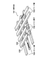
11 基板(シリコン基板)
20 磁性多層膜作製装置
27A,27B,27C 成膜チャンバ
Claims (4)
- 第1の強磁性層、第2の強磁性層、及び該第1の強磁性層と第2の強磁性層との間に位置するバリア層を有する積層構造、並びに、該第1の強磁性層の側に位置する基板を含む磁気抵抗効果素子であって、
前記バリア層は、前記第1の強磁性層との界面から前記第2の強磁性層との界面まで、層の厚さ方向において、(001)面が界面に平行に配向した単結晶構造の酸化マグネシウムを有し、前記第1の強磁性層は、CoFeBを含有することを特徴とする磁気抵抗効果素子。 - 前記第1の強磁性層は、前記バリア層の成膜時にアモルファスであることを特徴とする請求項1に記載の磁気抵抗効果素子。
- 前記バリア層は、酸化マグネシウムターゲットを用いたスパッタリング法で成膜された層であることを特徴とする請求項1記載の磁気抵抗効果素子。
- ワード線、
前記ワード線と交差配置したビット線、並びに、
前記ワード線と前記ビット線との間を接続するように配置した磁気抵抗効果素子及びトランジスタを有するMRAMであって、
前記磁気抵抗効果素子は、第1の強磁性層、第2の強磁性層及び前記第1の強磁性層と第2の強磁性層との間に位置し、前記第1の強磁性層との界面から前記第2の強磁性層との界面まで、層の厚さ方向において、(001)面が該層の界面に平行に配向した単結晶構造の酸化マグネシウム層を有する積層構造を有し、前記第1の強磁性層はCoFeBを含有することを特徴とするMRAM。
Priority Applications (1)
| Application Number | Priority Date | Filing Date | Title |
|---|---|---|---|
| JP2008259611A JP4774092B2 (ja) | 2008-10-06 | 2008-10-06 | 磁気抵抗効果素子およびそれを用いたmram |
Applications Claiming Priority (1)
| Application Number | Priority Date | Filing Date | Title |
|---|---|---|---|
| JP2008259611A JP4774092B2 (ja) | 2008-10-06 | 2008-10-06 | 磁気抵抗効果素子およびそれを用いたmram |
Related Parent Applications (1)
| Application Number | Title | Priority Date | Filing Date |
|---|---|---|---|
| JP2004259280A Division JP4292128B2 (ja) | 2004-09-07 | 2004-09-07 | 磁気抵抗効果素子の製造方法 |
Publications (2)
| Publication Number | Publication Date |
|---|---|
| JP2009044174A JP2009044174A (ja) | 2009-02-26 |
| JP4774092B2 true JP4774092B2 (ja) | 2011-09-14 |
Family
ID=40444499
Family Applications (1)
| Application Number | Title | Priority Date | Filing Date |
|---|---|---|---|
| JP2008259611A Expired - Lifetime JP4774092B2 (ja) | 2008-10-06 | 2008-10-06 | 磁気抵抗効果素子およびそれを用いたmram |
Country Status (1)
| Country | Link |
|---|---|
| JP (1) | JP4774092B2 (ja) |
Cited By (1)
| Publication number | Priority date | Publication date | Assignee | Title |
|---|---|---|---|---|
| US10680167B2 (en) | 2004-03-12 | 2020-06-09 | Japan Science And Technology Agency | Magnetic tunnel junction device |
Families Citing this family (1)
| Publication number | Priority date | Publication date | Assignee | Title |
|---|---|---|---|---|
| JP2013082961A (ja) * | 2011-10-07 | 2013-05-09 | Ulvac Japan Ltd | スパッタ装置 |
Family Cites Families (2)
| Publication number | Priority date | Publication date | Assignee | Title |
|---|---|---|---|---|
| JP2003124541A (ja) * | 2001-10-12 | 2003-04-25 | Nec Corp | 交換結合膜、磁気抵抗効果素子、磁気ヘッド及び磁気ランダムアクセスメモリ |
| US7884403B2 (en) * | 2004-03-12 | 2011-02-08 | Japan Science And Technology Agency | Magnetic tunnel junction device and memory device including the same |
-
2008
- 2008-10-06 JP JP2008259611A patent/JP4774092B2/ja not_active Expired - Lifetime
Cited By (4)
| Publication number | Priority date | Publication date | Assignee | Title |
|---|---|---|---|---|
| US10680167B2 (en) | 2004-03-12 | 2020-06-09 | Japan Science And Technology Agency | Magnetic tunnel junction device |
| US11233193B2 (en) | 2004-03-12 | 2022-01-25 | Japan Science And Technology Agency | Method of manufacturing a magnetorestive random access memeory (MRAM) |
| US11737372B2 (en) | 2004-03-12 | 2023-08-22 | Godo Kaisha Ip Bridge 1 | Method of manufacturing a magnetoresistive random access memory (MRAM) |
| US11968909B2 (en) | 2004-03-12 | 2024-04-23 | Godo Kaisha Ip Bridge 1 | Method of manufacturing a magnetoresistive random access memory (MRAM) |
Also Published As
| Publication number | Publication date |
|---|---|
| JP2009044174A (ja) | 2009-02-26 |
Similar Documents
| Publication | Publication Date | Title |
|---|---|---|
| JP4292128B2 (ja) | 磁気抵抗効果素子の製造方法 | |
| JP4774082B2 (ja) | 磁気抵抗効果素子の製造方法 | |
| US20100078310A1 (en) | Fabricating method of magnetoresistive element, and storage medium | |
| US20100080894A1 (en) | Fabricating method of magnetoresistive element, and storage medium | |
| US20110227018A1 (en) | Magnetoresistance element, method of manufacturing the same, and storage medium used in the manufacturing method | |
| US20110084348A1 (en) | Magnetoresistance element, method of manufacturing the same, and storage medium used in the manufacturing method | |
| JP4774092B2 (ja) | 磁気抵抗効果素子およびそれを用いたmram | |
| WO2010026725A1 (ja) | 磁気抵抗素子とその製造方法、該製造方法に用いる記憶媒体 | |
| JP4902686B2 (ja) | 磁気抵抗効果素子の製造方法 | |
| WO2010026703A1 (ja) | 磁気抵抗素子とその製造方法、該製造方法に用いる記憶媒体 | |
| JP4774116B2 (ja) | 磁気抵抗効果素子 | |
| WO2010026704A1 (ja) | 磁気抵抗素子とその製造方法、該製造方法に用いる記憶媒体 | |
| JP2009044173A (ja) | 磁性多層膜形成装置 | |
| WO2010029701A1 (ja) | 磁気抵抗素子とその製造方法、該製造方法に用いる記憶媒体 | |
| JPWO2010064564A1 (ja) | 磁気抵抗素子、その製造方法、および該製造方法に用いる記憶媒体 |
Legal Events
| Date | Code | Title | Description |
|---|---|---|---|
| A977 | Report on retrieval |
Free format text: JAPANESE INTERMEDIATE CODE: A971007 Effective date: 20110210 |
|
| A131 | Notification of reasons for refusal |
Free format text: JAPANESE INTERMEDIATE CODE: A131 Effective date: 20110222 |
|
| A521 | Request for written amendment filed |
Free format text: JAPANESE INTERMEDIATE CODE: A523 Effective date: 20110420 |
|
| TRDD | Decision of grant or rejection written | ||
| A01 | Written decision to grant a patent or to grant a registration (utility model) |
Free format text: JAPANESE INTERMEDIATE CODE: A01 Effective date: 20110607 |
|
| A01 | Written decision to grant a patent or to grant a registration (utility model) |
Free format text: JAPANESE INTERMEDIATE CODE: A01 |
|
| A61 | First payment of annual fees (during grant procedure) |
Free format text: JAPANESE INTERMEDIATE CODE: A61 Effective date: 20110624 |
|
| FPAY | Renewal fee payment (event date is renewal date of database) |
Free format text: PAYMENT UNTIL: 20140701 Year of fee payment: 3 |
|
| R150 | Certificate of patent or registration of utility model |
Ref document number: 4774092 Country of ref document: JP Free format text: JAPANESE INTERMEDIATE CODE: R150 Free format text: JAPANESE INTERMEDIATE CODE: R150 |
|
| R250 | Receipt of annual fees |
Free format text: JAPANESE INTERMEDIATE CODE: R250 |
|
| S533 | Written request for registration of change of name |
Free format text: JAPANESE INTERMEDIATE CODE: R313533 |
|
| R350 | Written notification of registration of transfer |
Free format text: JAPANESE INTERMEDIATE CODE: R350 |
|
| R250 | Receipt of annual fees |
Free format text: JAPANESE INTERMEDIATE CODE: R250 |
|
| R250 | Receipt of annual fees |
Free format text: JAPANESE INTERMEDIATE CODE: R250 |
|
| R250 | Receipt of annual fees |
Free format text: JAPANESE INTERMEDIATE CODE: R250 |
|
| R250 | Receipt of annual fees |
Free format text: JAPANESE INTERMEDIATE CODE: R250 |
|
| R250 | Receipt of annual fees |
Free format text: JAPANESE INTERMEDIATE CODE: R250 |
|
| R250 | Receipt of annual fees |
Free format text: JAPANESE INTERMEDIATE CODE: R250 |
|
| R250 | Receipt of annual fees |
Free format text: JAPANESE INTERMEDIATE CODE: R250 |
|
| R250 | Receipt of annual fees |
Free format text: JAPANESE INTERMEDIATE CODE: R250 |
|
| R250 | Receipt of annual fees |
Free format text: JAPANESE INTERMEDIATE CODE: R250 |
|
| R250 | Receipt of annual fees |
Free format text: JAPANESE INTERMEDIATE CODE: R250 |
|
| EXPY | Cancellation because of completion of term |