JP4768039B2 - Display drive device and display device - Google Patents
Display drive device and display device Download PDFInfo
- Publication number
- JP4768039B2 JP4768039B2 JP2009048655A JP2009048655A JP4768039B2 JP 4768039 B2 JP4768039 B2 JP 4768039B2 JP 2009048655 A JP2009048655 A JP 2009048655A JP 2009048655 A JP2009048655 A JP 2009048655A JP 4768039 B2 JP4768039 B2 JP 4768039B2
- Authority
- JP
- Japan
- Prior art keywords
- switch
- voltage
- source line
- signal
- display
- Prior art date
- Legal status (The legal status is an assumption and is not a legal conclusion. Google has not performed a legal analysis and makes no representation as to the accuracy of the status listed.)
- Expired - Fee Related
Links
Images


Classifications
-
- G—PHYSICS
- G09—EDUCATION; CRYPTOGRAPHY; DISPLAY; ADVERTISING; SEALS
- G09G—ARRANGEMENTS OR CIRCUITS FOR CONTROL OF INDICATING DEVICES USING STATIC MEANS TO PRESENT VARIABLE INFORMATION
- G09G3/00—Control arrangements or circuits, of interest only in connection with visual indicators other than cathode-ray tubes
- G09G3/20—Control arrangements or circuits, of interest only in connection with visual indicators other than cathode-ray tubes for presentation of an assembly of a number of characters, e.g. a page, by composing the assembly by combination of individual elements arranged in a matrix no fixed position being assigned to or needed to be assigned to the individual characters or partial characters
- G09G3/22—Control arrangements or circuits, of interest only in connection with visual indicators other than cathode-ray tubes for presentation of an assembly of a number of characters, e.g. a page, by composing the assembly by combination of individual elements arranged in a matrix no fixed position being assigned to or needed to be assigned to the individual characters or partial characters using controlled light sources
- G09G3/30—Control arrangements or circuits, of interest only in connection with visual indicators other than cathode-ray tubes for presentation of an assembly of a number of characters, e.g. a page, by composing the assembly by combination of individual elements arranged in a matrix no fixed position being assigned to or needed to be assigned to the individual characters or partial characters using controlled light sources using electroluminescent panels
- G09G3/32—Control arrangements or circuits, of interest only in connection with visual indicators other than cathode-ray tubes for presentation of an assembly of a number of characters, e.g. a page, by composing the assembly by combination of individual elements arranged in a matrix no fixed position being assigned to or needed to be assigned to the individual characters or partial characters using controlled light sources using electroluminescent panels semiconductive, e.g. using light-emitting diodes [LED]
- G09G3/3208—Control arrangements or circuits, of interest only in connection with visual indicators other than cathode-ray tubes for presentation of an assembly of a number of characters, e.g. a page, by composing the assembly by combination of individual elements arranged in a matrix no fixed position being assigned to or needed to be assigned to the individual characters or partial characters using controlled light sources using electroluminescent panels semiconductive, e.g. using light-emitting diodes [LED] organic, e.g. using organic light-emitting diodes [OLED]
- G09G3/3275—Details of drivers for data electrodes
- G09G3/3291—Details of drivers for data electrodes in which the data driver supplies a variable data voltage for setting the current through, or the voltage across, the light-emitting elements
-
- G—PHYSICS
- G09—EDUCATION; CRYPTOGRAPHY; DISPLAY; ADVERTISING; SEALS
- G09G—ARRANGEMENTS OR CIRCUITS FOR CONTROL OF INDICATING DEVICES USING STATIC MEANS TO PRESENT VARIABLE INFORMATION
- G09G2310/00—Command of the display device
- G09G2310/02—Addressing, scanning or driving the display screen or processing steps related thereto
- G09G2310/0264—Details of driving circuits
- G09G2310/027—Details of drivers for data electrodes, the drivers handling digital grey scale data, e.g. use of D/A converters
-
- G—PHYSICS
- G09—EDUCATION; CRYPTOGRAPHY; DISPLAY; ADVERTISING; SEALS
- G09G—ARRANGEMENTS OR CIRCUITS FOR CONTROL OF INDICATING DEVICES USING STATIC MEANS TO PRESENT VARIABLE INFORMATION
- G09G2330/00—Aspects of power supply; Aspects of display protection and defect management
- G09G2330/02—Details of power systems and of start or stop of display operation
- G09G2330/021—Power management, e.g. power saving
- G09G2330/023—Power management, e.g. power saving using energy recovery or conservation
-
- G—PHYSICS
- G09—EDUCATION; CRYPTOGRAPHY; DISPLAY; ADVERTISING; SEALS
- G09G—ARRANGEMENTS OR CIRCUITS FOR CONTROL OF INDICATING DEVICES USING STATIC MEANS TO PRESENT VARIABLE INFORMATION
- G09G3/00—Control arrangements or circuits, of interest only in connection with visual indicators other than cathode-ray tubes
- G09G3/20—Control arrangements or circuits, of interest only in connection with visual indicators other than cathode-ray tubes for presentation of an assembly of a number of characters, e.g. a page, by composing the assembly by combination of individual elements arranged in a matrix no fixed position being assigned to or needed to be assigned to the individual characters or partial characters
- G09G3/22—Control arrangements or circuits, of interest only in connection with visual indicators other than cathode-ray tubes for presentation of an assembly of a number of characters, e.g. a page, by composing the assembly by combination of individual elements arranged in a matrix no fixed position being assigned to or needed to be assigned to the individual characters or partial characters using controlled light sources
- G09G3/30—Control arrangements or circuits, of interest only in connection with visual indicators other than cathode-ray tubes for presentation of an assembly of a number of characters, e.g. a page, by composing the assembly by combination of individual elements arranged in a matrix no fixed position being assigned to or needed to be assigned to the individual characters or partial characters using controlled light sources using electroluminescent panels
- G09G3/32—Control arrangements or circuits, of interest only in connection with visual indicators other than cathode-ray tubes for presentation of an assembly of a number of characters, e.g. a page, by composing the assembly by combination of individual elements arranged in a matrix no fixed position being assigned to or needed to be assigned to the individual characters or partial characters using controlled light sources using electroluminescent panels semiconductive, e.g. using light-emitting diodes [LED]
- G09G3/3208—Control arrangements or circuits, of interest only in connection with visual indicators other than cathode-ray tubes for presentation of an assembly of a number of characters, e.g. a page, by composing the assembly by combination of individual elements arranged in a matrix no fixed position being assigned to or needed to be assigned to the individual characters or partial characters using controlled light sources using electroluminescent panels semiconductive, e.g. using light-emitting diodes [LED] organic, e.g. using organic light-emitting diodes [OLED]
- G09G3/3225—Control arrangements or circuits, of interest only in connection with visual indicators other than cathode-ray tubes for presentation of an assembly of a number of characters, e.g. a page, by composing the assembly by combination of individual elements arranged in a matrix no fixed position being assigned to or needed to be assigned to the individual characters or partial characters using controlled light sources using electroluminescent panels semiconductive, e.g. using light-emitting diodes [LED] organic, e.g. using organic light-emitting diodes [OLED] using an active matrix
Landscapes
- Engineering & Computer Science (AREA)
- Physics & Mathematics (AREA)
- Computer Hardware Design (AREA)
- General Physics & Mathematics (AREA)
- Theoretical Computer Science (AREA)
- Control Of Indicators Other Than Cathode Ray Tubes (AREA)
- Electroluminescent Light Sources (AREA)
- Control Of El Displays (AREA)
Description
本発明はテレビジョン受像機、パーソナルコンピュータ、ワークステーション等に用いる表示装置および表示駆動装置に関するものである。 The present invention relates to a display device and a display driving device used for a television receiver, a personal computer, a workstation and the like.
従来、液晶表示パネルでは、陽の映像信号と陰の映像信号を交互に駆動する、いわゆる、反転駆動が用いられる場合がある。この反転駆動において、消費電力削減のため駆動期間中にIC内の隣接する端子をショートさせ、電荷の再利用を行う技術がある(たとえば、特許文献1参照)。 Conventionally, in a liquid crystal display panel, a so-called inversion drive in which a positive video signal and a negative video signal are alternately driven may be used. In this inversion driving, there is a technique for reusing electric charges by shorting adjacent terminals in an IC during a driving period in order to reduce power consumption (see, for example, Patent Document 1).
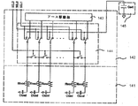
図11は、前記特許文献1に記載された、省電力化回路を図る従来の反転駆動方式の表示装置の構成図である。
FIG. 11 is a configuration diagram of a conventional inversion drive type display device described in the above-mentioned
図11において、液晶パネル141は、ソース駆動部143とラインスイッチング部144によって構成されたソースドライバ142によって駆動され、さらに外部キャパシター145が接続された構成となっている。また、液晶パネル141の駆動方式の特徴である反転駆動方式として、図12は、従来の反転駆動における陽の映像信号および陰の映像信号を示す図である。同図における陽の映像信号、陰の映像信号は、ソースドライバ142から液晶パネル141に交互に供給される。
従来の表示装置では、特許文献1に示す通り、陽の映像信号と陰の映像信号を交互に駆動するため(いわゆる、反転駆動を行うため)、その中間の信号レベルを通過することとなり有効であるが、たとえば有機ELパネルのように陽の映像信号と陰の映像信号を交互に駆動しない方式(いわゆる反転駆動ができない方式)については、隣接する端子を単にショートさせ外部キャパシターによる電荷の再利用はできず、省電力化が難しいという課題を有している。
In the conventional display device, as shown in
また、近年の多出力化、高負荷高速駆動によりICの発熱が課題となっている。
この発明は、上記従来の課題を解決するものであり、電荷の再利用を行い省電力化を図ると共に、発熱を低減する表示駆動装置および表示装置を提供することを目的とする。
Further, due to the recent increase in the number of outputs and the high load and high speed driving, heat generation of the IC has become a problem.
SUMMARY OF THE INVENTION An object of the present invention is to solve the above-described conventional problems, and to provide a display driving device and a display device that reduce power generation by reusing charges to reduce power consumption.
上記課題を解決するため本発明の表示駆動装置は、画素列毎にソースラインを有する表示パネルを駆動する表示駆動装置であって、ソースライン毎に設けられた第1スイッチと、ソースライン毎に設けられた第2スイッチと、ソースライン毎に設けられ、前記第2スイッチを介して当該ソースラインに画素信号を駆動するドライバと、前記画素信号の最大電圧と最小電圧の間の電圧である中間電圧を中間電圧線に出力する電源部と、各第1スイッチおよび各第2スイッチのオンおよびオフを制御する制御部とを備え、各第1スイッチの一端は前記中間電圧線に、他端は対応するソースラインに接続され、各第2スイッチの一端は前記ドライバに、他端は対応するソースラインおよび対応する前記第1スイッチの他端に接続され、前記制御部は、画素信号の出力期間と次の画素信号の出力期間との間の切り替え期間において、第2スイッチを一時的にオフにするとともに、当該第2スイッチに対応する前記第1スイッチを一時的にオンにする。 In order to solve the above problems, a display driving device of the present invention is a display driving device for driving a display panel having a source line for each pixel column, and includes a first switch provided for each source line and each source line. A second switch provided, a driver provided for each source line and driving a pixel signal to the source line via the second switch, and an intermediate voltage between the maximum voltage and the minimum voltage of the pixel signal A power supply unit that outputs a voltage to an intermediate voltage line; and a control unit that controls on and off of each first switch and each second switch, one end of each first switch being connected to the intermediate voltage line and the other end being Connected to the corresponding source line, one end of each second switch connected to the driver, the other end connected to the corresponding source line and the other end of the corresponding first switch, and the control unit In the switching period between the output period of the pixel signal and the output period of the next pixel signal, the second switch is temporarily turned off and the first switch corresponding to the second switch is temporarily turned on. To do.
この構成によれば、反転駆動を行わない表示パネル、例えば有機EL表示パネルにおいて、電荷再利用により発熱を低減し、加えて、再利用できない電荷変動を電源部に吸収させることによって表示駆動装置および表示パネルの発熱および消費電力を低減することができる。 According to this configuration, in a display panel that does not perform inversion driving, for example, an organic EL display panel, heat generation is reduced by charge reuse, and in addition, a change in charge that cannot be reused is absorbed by the power supply unit, and Heat generation and power consumption of the display panel can be reduced.
より詳しく説明すると、上記の切り替え期間において、第1スイッチは、全部または一部のソースライン同士を短絡し、かつ当該ソースラインを電源部に接続する。第2スイッチは、切り替え期間において、当該ソースラインをドライバから切り離す。例えば、ソースラインの総数が約6000本あるものとする。6000本のうち、上記の短絡直前において4000本が中間電圧よりも高く、2000本が中間電圧よりも低いとする。上記の短絡により、中間電圧よりも低い電圧の2000本と、中間電圧よりも電圧が高い4000本のうちの2000本とは、逆向きの電荷変動を相殺することになる(つまり電荷の再利用をすることになる)。これにより、発熱を低減することができる。なぜなら、逆向きの電荷変動を相殺できない従来技術では、全ての電荷変動をドライバが吸収し(つまりドライバに電流が流れ)、発熱するからである。 More specifically, in the switching period, the first switch short-circuits all or some of the source lines and connects the source lines to the power supply unit. The second switch disconnects the source line from the driver during the switching period. For example, it is assumed that the total number of source lines is about 6000. Of the 6000 lines, 4,000 lines are higher than the intermediate voltage and 2000 lines are lower than the intermediate voltage immediately before the short circuit. Due to the short circuit described above, 2000 having a voltage lower than the intermediate voltage and 2000 out of 4000 having a voltage higher than the intermediate voltage cancel out charge fluctuations in the opposite direction (that is, charge reuse). Will do.) Thereby, heat generation can be reduced. This is because in the conventional technology that cannot cancel the charge fluctuation in the opposite direction, the driver absorbs all charge fluctuations (that is, current flows through the driver) and generates heat.
さらに、中間電圧よりも電圧が高い4000本のうちの相殺されない2000本の電荷の変動は、第1スイッチを介して電源部に吸収される。これにより、ドライバでの発熱を電源部に転嫁することができる。 Further, the fluctuation of 2000 charges that are not canceled out of 4000 whose voltage is higher than the intermediate voltage is absorbed by the power supply unit via the first switch. Thereby, the heat generated by the driver can be transferred to the power supply unit.
このように、切り替え期間において、全部または一部のソースライン同士が短絡し、かつ当該ソースラインが電源部に接続される。これにより、短絡直前に中間電圧よりも高い電圧のソースラインと、短絡直前に中間電圧よりも低い電圧のソースラインとが電荷を相殺し合う。短絡しない場合にドライバが画素信号の電圧変化による電荷移動を全て吸収する必要がなく、発熱を低減することができる。加えて、相殺できない電荷は、ドライバではなく電源部が電荷の変動を吸収するので、ドライバでの発熱を電源部に転嫁することができる。 Thus, in the switching period, all or some of the source lines are short-circuited, and the source lines are connected to the power supply unit. Thereby, the source line having a voltage higher than the intermediate voltage just before the short circuit and the source line having a voltage lower than the intermediate voltage just before the short circuit cancel each other out. When not short-circuited, it is not necessary for the driver to absorb all the charge transfer due to the voltage change of the pixel signal, and heat generation can be reduced. In addition, since the electric power that cannot be canceled out is absorbed by the power source unit, not the driver, in the power source unit, heat generated by the driver can be transferred to the power source unit.
ここで、前記ドライバ、第1スイッチ、第2スイッチおよび制御部は第1の半導体基板に形成され、前記電源部は第2の半導体基板に形成されるようにしてもよい。 Here, the driver, the first switch, the second switch, and the control unit may be formed on a first semiconductor substrate, and the power supply unit may be formed on a second semiconductor substrate.
この構成によれば、電源部はドライバと異なる半導体基板に形成されるので、ドライバの発熱をより効率よく低減することができる。 According to this configuration, since the power supply unit is formed on a semiconductor substrate different from that of the driver, the heat generation of the driver can be reduced more efficiently.
ここで、前記制御部は、前記切り替え期間において、全ての第2スイッチを一時的にオフにするとともに、当該第2スイッチに対応する全ての前記第1スイッチを一時的にオンにするようにしてもよい。 Here, the control unit temporarily turns off all the second switches and temporarily turns on all the first switches corresponding to the second switches in the switching period. Also good.
この構成によれば、制御部の回路構成を簡単にすることができ、回路規模を少なくすることができる。 According to this configuration, the circuit configuration of the control unit can be simplified and the circuit scale can be reduced.
ここで、前記制御部は、ソースライン毎に設けられた制御回路を有し、各制御回路は、対応するソースラインの画素信号と次の画素信号とが前記中間電圧をまたぐとき、前記切り替え期間において対応する第1スイッチおよび第2スイッチの一時的なオンおよびオフを行い、対応するソースラインの画素信号と次の画素信号とが前記中間電圧をまたがないとき、前記切り替え期間において対応する第1スイッチおよび第2スイッチの状態を維持するようにしてもよい。 Here, the control unit has a control circuit provided for each source line, and each control circuit has the switching period when the pixel signal of the corresponding source line and the next pixel signal cross the intermediate voltage. When the corresponding first switch and second switch are temporarily turned on and off in step, and the pixel signal of the corresponding source line and the next pixel signal do not cross the intermediate voltage, the corresponding first switch and second switch are switched in the switching period. You may make it maintain the state of 1 switch and 2nd switch.
この構成によれば、ソースラインの画素信号と次の画素信号とが中間電圧をまたがないとき、当該ソースラインを電源部に接続しないので、発熱をさらに低減し、消費電力をより低減することができる。 According to this configuration, when the pixel signal of the source line and the next pixel signal do not cross the intermediate voltage, the source line is not connected to the power supply unit, so that heat generation is further reduced and power consumption is further reduced. Can do.
ここで、前記中間電圧線は、第1スイッチを介して第1の色に対応するソースラインに接続される第1電圧線と、第1スイッチを介して第2の色に対応するソースラインに接続される第2電圧線とを含み、前記電源部は、第1の色を表す画素信号の最大電圧と最小電圧の中間値である第1電圧を前記中間電圧として出力し、第2の色を表す画素信号の最大電圧と最小電圧の中間値である第2電圧を前記中間電圧として出力するようにしてもよい。 Here, the intermediate voltage line is connected to the first voltage line connected to the source line corresponding to the first color via the first switch and the source line corresponding to the second color via the first switch. A second voltage line connected, and the power supply unit outputs, as the intermediate voltage, a first voltage that is an intermediate value between a maximum voltage and a minimum voltage of the pixel signal representing the first color, and the second color A second voltage, which is an intermediate value between the maximum voltage and the minimum voltage of the pixel signal representing, may be output as the intermediate voltage.
この構成によれば、色毎に画素信号の電圧範囲が異なる場合に、電荷再利用の効率を上げ、さらに消費電力を低減することができる。 According to this configuration, when the voltage range of the pixel signal is different for each color, it is possible to increase the efficiency of charge reuse and further reduce power consumption.
ここで、さらに、前記中間電圧線と各第1スイッチとの間に挿入された第3スイッチを備え、前記制御部は、第1スイッチをオンにした後に第3スイッチを一時的にオンするようにしてもよい。 Here, a third switch inserted between the intermediate voltage line and each first switch is further provided, and the control unit temporarily turns on the third switch after turning on the first switch. It may be.
この構成によれば、第1スイッチによりソースライン同士を短絡した直後に、第3スイッチによりソースラインを電源部に接続するので、同時に接続する場合と比べて、ノイズおよび貫通電流の発生を抑えることができる。 According to this configuration, since the source line is connected to the power supply unit by the third switch immediately after the source lines are short-circuited by the first switch, generation of noise and through current can be suppressed as compared with the case of connecting simultaneously. Can do.
また、本発明の表示装置は上記の表示駆動装置と、前記表示駆動装置によって駆動される表示パネルとを備える。 The display device of the present invention includes the above display driving device and a display panel driven by the display driving device.
ここで、前記表示パネルは有機ELパネルであってもよい。 Here, the display panel may be an organic EL panel.
本発明の表示装置によれば、反転駆動を行わない表示装置、たとえば有機ELにおいても、電荷再利用の実現が可能となり、かつ電源を外部に持つことによる発熱を低減し、省電力化を図ることができる。 According to the display device of the present invention, even in a display device that does not perform inversion driving, for example, an organic EL, charge reuse can be realized, and heat generation due to having a power source outside is reduced, thereby saving power. be able to.
(第1の実施形態)
図1、図2は、本発明の第1の実施形態に係る表示装置、表示駆動装置の構成例を示すものである。
(First embodiment)
1 and 2 show a configuration example of a display device and a display driving device according to the first embodiment of the present invention.
図1は本実施形態に係る表示装置の全体構成図である。この表示装置は、表示パネルとしての有機ELパネル41と、ソースドライバ43と、外部電源48と、ゲートドライバ49とを備える。
FIG. 1 is an overall configuration diagram of a display device according to the present embodiment. This display device includes an
有機ELパネル41は、行列上に配置された複数の画素42と、画素の列毎に設けられたソースライン45と、画素の行毎に設けられたゲートライン46とを有する。
The
ソースドライバ43は、外部電源48とともに、画素列毎にソースラインを有する表示パネルを駆動する表示駆動装置として機能する。
The
この表示駆動装置は、ソースライン45毎に設けられた第1スイッチsw1と、ソースライン45毎に設けられた第2スイッチsw2と、ソースライン45毎に設けられ、前記第2スイッチsw2を介して当該ソースライン45に画素信号を駆動するドライバとしてのAMP部52と、前記画素信号の最大電圧と最小電圧の間の電圧である中間電圧を中間電圧線に出力する外部電源48と、各第1スイッチsw1および各第2スイッチsw2のオンおよびオフを制御する制御回路47とを備える。
The display driving device is provided with a first switch sw1 provided for each
ソースドライバ43は、ソースライン毎に設けられた駆動部44と、制御回路47とを有する。
The
各第1スイッチsw1の一端は前記中間電圧線に、他端は対応するソースラインに接続される。 Each first switch sw1 has one end connected to the intermediate voltage line and the other end connected to the corresponding source line.
各第2スイッチsw2の一端は前記AMP部52に、他端は対応するソースライン45および対応する前記第1スイッチsw1の他端に接続される。
One end of each second switch sw2 is connected to the
制御回路47は、画素信号の出力期間と次の画素信号の出力期間との間の切り替え期間において、第2スイッチsw2を一時的にオフにするとともに、当該第2スイッチsw2に対応する第1スイッチsw1を一時的にオンにする。
The
制御回路47が第1スイッチsw1および第2スイッチsw2を制御することにより、切り替え期間において、全部または一部のソースライン同士が短絡し、かつ当該ソースラインが電源部に接続される。これにより、短絡直前に中間電圧よりも高い電圧のソースラインと、短絡直前に中間電圧よりも低い電圧のソースラインとが電荷を相殺し合う。短絡しない場合にドライバが画素信号の電圧変化による電荷移動を全て吸収する必要がなく、発熱を低減することができる。加えて、相殺できない電荷は、ドライバではなく電源部が電荷の変動を吸収するので、ドライバでの発熱を電源部に転嫁することができる。
When the
駆動部44は、各ソースラインに対応して設けられ、図1の破線で示すように、制御回路51と、ドライバとしてのAMP部52と、第1スイッチsw1と第2スイッチsw2とを含む。
The
次に、図2は本実施形態に係る表示駆動装置内の駆動部44の詳細な構成例を示す図である。具体的には、ソースライン45を駆動するための駆動部44と、外部電源48と、制御回路47からの制御1信号および制御2信号との接続を示すものである。同図のように、駆動部44は、制御回路51と、AMP部52と、第1スイッチsw1と、第2スイッチsw2とを備える。制御回路51は、第1ラッチ54と、第2ラッチ55と、セレクト部53とを備える。
Next, FIG. 2 is a diagram illustrating a detailed configuration example of the driving
第1ラッチ54は、デジタルのデータ信号として転送される画像データをデータ取込信号によって記憶する。第2ラッチ55は、第1ラッチ54の出力をデータ転送信号によって記憶する。第2ラッチ55の出力はデジタル信号をアナログ信号に変換するデジタル−アナログ変換器であるセレクト部53に入力される。セレクト部53によって変換されたアナログ信号はAMP部52に入力される。AMP部52は、アナログ画素信号を第2スイッチsw2を介してソースライン45に駆動するドライバとして機能する。
The
また、AMP部52の出力は第2スイッチsw2を介してソースライン45に接続される。第2スイッチsw2は制御2信号により制御される。外部電源48は、第2スイッチsw2のソースライン側に接続され、かつ制御1信号によって制御される第1スイッチsw1を介してソースライン45に接続される。
The output of the
次に、図3を用いて、第1の実施形態における表示装置、表示駆動装置の動作を説明する。図3は第1の実施形態に係る表示装置の動作タイミングを示すタイムチャート図である。 Next, the operation of the display device and the display driving device in the first embodiment will be described with reference to FIG. FIG. 3 is a time chart showing the operation timing of the display device according to the first embodiment.
図3において、有機ELパネル41に複数存在するゲートライン46のうちの3ラインの信号レベル状態をゲート信号1、ゲート信号2、ゲート信号3とする。また有機ELパネル41に複数存在するソースライン45のうちの2ラインの信号レベル状態をソース信号1、ソース信号2とする。また、それぞれのソース信号の出力範囲の中間電位を破線で表す。
In FIG. 3, the signal levels of three lines among the plurality of
なお、図3において、データ転送信号、制御1信号、制御2信号は図2に示した信号である。第1ラッチ54の出力は第1ラッチデータ、第2ラッチ55の出力は第2ラッチデータとしてある。
In FIG. 3, the data transfer signal, the
また、図3において、ゲート信号1の立ち上がりをt61、ゲート信号2の立ち上がりをt63、ゲート信号3の立ち上がりをt65、データ転送信号の立ち下がりをt52、t54、t66とする。
In FIG. 3, the rising edge of the
図3より、まず始めに、データ信号として伝送される画素データは、データ取込信号によって第1ラッチ54に取り込まれる。
As shown in FIG. 3, first, pixel data transmitted as a data signal is taken into the
次に、この動作をソースドライバ43を構成するIC内のすべての駆動部44に対し順に行われる。すべての駆動部44に所望の画素データが第1ラッチ54の取り込まれた後、データ転送信号の立ち上がりt61に同期して第2ラッチ55にデータ転送されると同時に、ゲート信号1が立ち上がり、ゲート信号1に接続された複数の画素が、ソースライン45からの駆動可能状態となる。
Next, this operation is sequentially performed on all the
次に、第2ラッチ55に転送された画像データはセレクト部53へ入力される。セレクト部53によりデジタルからアナログに変換されたアナログ電圧はAMP部52へ伝達される。さらに、ソースライン45へAMP部52によって駆動された電圧が画素信号として出力される。制御1信号がハイの時、第1スイッチsw1は接続状態となり、ロウの時、第1スイッチsw1は切断状態となる。
Next, the image data transferred to the
次に、制御2信号がハイの時、第2スイッチsw2は接続状態となり、ロウの時、第2スイッチsw2は切断状態となる。
Next, when the
次に、制御1信号はデータ転送信号58に同期してハイになり、制御2信号はロウになることにより、第1スイッチsw1が接続状態、第2スイッチsw2は切断状態になり、ソースライン45は外部電源48の中間電圧線に接続され、t61からt62の間は各ソースライン45には外部電源48より供給される中間電圧が印加される。
Next, the
その後、制御1信号がロウ、制御2信号がハイになることにより、第1スイッチsw1が切断され、第2スイッチsw2が接続されることにより、ソースライン45にはAMP部52が接続され、画像データに応じた電圧がソースライン45に印加される。
Thereafter, when the
この動作をゲート信号2、ゲート信号3、・・・と、有機ELパネル41の全ゲートライン46毎に繰り返すことにより、ゲート信号がハイ区間の画素42に画像データに対応した電圧が印加され、順に全ラインへの電圧印加を繰り返すことにより、1フレームの表示がされる。
By repeating this operation for each of the
以上、図面を用いて説明した本発明の第1の実施形態に係る表示装置および表示駆動装置は、たとえば、パネルすべてのソースラインの半分が11V、残りの半分が1Vを印加していた状態であったとすると、制御1信号がハイ、かつ制御2信号がロウの時、一度外部電源48により全ソースライン45に11Vと1Vの中間である6Vを印加することにより、すべてのソースラインは6Vに収束する。
As described above, in the display device and the display driving device according to the first embodiment of the present invention described with reference to the drawings, for example, 11V is applied to half of the source lines of all the panels and 1V is applied to the other half. If the
この場合、11Vのソースラインと1Vのソースラインの数がちょうど半分であるため、電荷保存則により、11Vのソースラインから1Vのソースラインへ電荷が移動するため、外部電源からの電荷の供給は発生することなしに、6Vまでの電荷の供給をソースドライバ43から行うことなしに実施することが出来る。
In this case, since the number of 11V source lines and 1V source lines is exactly half, the charge is transferred from the 11V source line to the 1V source line according to the charge conservation law. Without being generated, it is possible to supply electric charges up to 6 V without performing the supply from the
すなわち、本発明の第1の実施形態に係る表示装置は、陽の映像信号と陰の映像信号を交互に駆動しない(いわゆる反転駆動しない)有機ELパネル41においても、常に外部電源48により一度中間電位を印加することができ、有機ELパネル41への充放電電力は半分に抑えることが出来るため、省電力化が可能となる。
That is, in the display device according to the first embodiment of the present invention, even in the
さらに、有機ELパネルの動作において、映像を表示する場合、11Vのソースラインと1Vのソースラインの数がちょうど半分になることはほぼ無い。 Furthermore, in the operation of the organic EL panel, when displaying an image, the number of 11V source lines and 1V source lines are almost never halved.
その理由は、FHDパネル(フルハイビジョンパネル)の場合、ソースラインは1920×3の5760ライン存在し、たとえば、11Vのソースラインが3840ライン、1Vのソースラインが1920ラインであった場合、制御1信号がハイ、かつ制御2信号がロウの時、電荷保存則により(11V−1V)×2/3+1V=約7.7Vに収束し、外部電源48により6Vへ強制的に収束されるためである。
The reason is that, in the case of an FHD panel (full high-definition panel), there are 1920 × 3 5760 lines. For example, if the source line of 11V is 3840 lines and the source line of 1V is 1920 lines,
しかし、本発明は外部電源48がソースドライバ43と異なる半導体基板に形成されている、或いは外部にある。
However, in the present invention, the
これにより、約7.7V−6V=約1.7Vの電位差を供給するための電力は外部電源48によって発生し、その電力に応じて外部電源48は発熱する。
As a result, electric power for supplying a potential difference of about 7.7 V−6 V = about 1.7 V is generated by the
すなわち、本発明の第1の実施形態に係る表示装置、表示駆動装置では、従来ソースドライバ43で駆動していた約1.7V分の電力による発熱を外部電源48に移すことにより、ソースドライバ43の発熱量を減らすことができる。
That is, in the display device and the display driving device according to the first embodiment of the present invention, the
さらに、発熱量を減らすことによりソースドライバ43を更に多出力化することができる。
Furthermore, the output of the
すなわち、ソースドライバの使用数を減らすことによる有機ELパネルのコスト削減が出来る。 That is, the cost of the organic EL panel can be reduced by reducing the number of source drivers used.
(第2の実施形態)
第1の実施形態では切り替え期間において全ソースライン45を短絡させて外部電源48に接続する例を説明した。つづいて、第2の実施形態では、切り替え期間において一部のソースライン45を短絡させて外部電源48に接続する表示制御部の構成について説明する。
(Second Embodiment)
In the first embodiment, the example in which all the source lines 45 are short-circuited and connected to the
すなわち、第2の実施形態の表示制御部は、ソースライン毎に設けられた制御回路を有し、各制御回路は、対応するソースラインの画素信号と次の画素信号とが外部電源48の中間電圧をまたぐとき、前記切り替え期間において対応する第1スイッチおよび第2スイッチの一時的なオンおよびオフを行い、対応するソースラインの画素信号と次の画素信号とが前記中間電圧をまたがないとき、前記切り替え期間において対応する第1スイッチおよび第2スイッチの状態を維持するように構成されている。
In other words, the display control unit of the second embodiment has a control circuit provided for each source line, and each control circuit has a pixel signal of the corresponding source line and the next pixel signal between the
図4は第2の実施形態に係る表示装置の全体構成図である。同図の表示装置は図1に示した表示装置と比較して、ソースドライバ43の代わりにソースドライバ73を備える点が異なっている。同じ構成要素には同じ符号を付しているので、以下では同じ点は説明を省略して異なる点を中心に説明する。
FIG. 4 is an overall configuration diagram of a display device according to the second embodiment. The display device shown in the figure is different from the display device shown in FIG. 1 in that a
ソースドライバ73は、図1のソースドライバ43と比べて、制御回路47が削除された点と、駆動部44の代わりに駆動部74を備える点とが異なっている。
The
駆動部74は、制御回路71、AMP部52、第1スイッチsw1、第2スイッチsw2を備える。
The
制御回路71は、図1の制御回路51の機能に加えて、現在の画素信号と次の画素信号とを比較し、比較の結果、現在の画素信号と次の画素信号とが前記中間電圧をまたぐか否かを判定し、判定結果に応じて、切り替え期間において第1スイッチおよび第2スイッチの一時的なオンおよびオフを行うか、第1スイッチおよび第2スイッチの状態を維持するかを決定する。
In addition to the function of the
すなわち、制御回路71は、現在の画素信号と次の画素信号とが前記中間電圧をまたぐとき、前記切り替え期間において対応する第1スイッチおよび第2スイッチの一時的なオンおよびオフを行い、一方、画素信号と次の画素信号とが前記中間電圧をまたがないとき、前記切り替え期間において対応する第1スイッチおよび第2スイッチの状態を維持する。
That is, when the current pixel signal and the next pixel signal cross the intermediate voltage, the
図5は第2の実施形態に係る表示駆動装置内の駆動部74の詳細な構成例を示す図である。同図の駆動部74は、図4の駆動部44と比べて、比較回路91が追加されている点が異なっている。
FIG. 5 is a diagram illustrating a detailed configuration example of the driving
比較回路91は、現在の画素信号(第2ラッチ55の画素データ)と次の画素信号(第1ラッチ54の画素データ)とを比較し、比較結果に応じて制御1信号および制御2信号を生成する回路である。
The
図6は第2の実施形態に係る比較回路91の詳細な構成例を示す図である。同図の比較回路91は、比較器96、ラッチ97、アンドゲート98、ナンドゲート99を備える。
FIG. 6 is a diagram illustrating a detailed configuration example of the
比較器96は、現在の画素信号(第2ラッチ55の画素データ)と次の画素信号(第1ラッチ54の画素データ)が前記中間電圧(画素データの中央値)をまたぐか否かを判定する。同図では、比較器96は、第2ラッチ55の画素データのMSB(最上位ビット)と第1ラッチ54の画素データのMSBとが一致するか否かを判定する排他的論理和回路でよい。この場合、比較器96は、両MSBが一致しない場合は、両データが画素データの中央値をまたぐことを示す”1”出力し、両MSBが一致する場合は、両データが画素データの中央値をまたがないことを示す”0”を出力する。比較器96は、画素データがアナログ電圧に変換される前のデジタル画素データを比較するので、簡単な回路により実現することができる。
The
ラッチ97は、比較器96の比較結果つまり、両MSBが一致しないか一致するかを示す1ビットのフラグをデータ比較信号のタイミングで取り込み保持する。
The
アンドゲート98は、ラッチ97に保持されたフラグが1のとき(上記両データが上記中央値をまたぐとき)データ転送信号に同期して制御1信号を出力し、ラッチ97に保持されたフラグが”0”のとき(上記両データが上記中央値をまたがないとき)データ転送信号に係わらず同期して制御1信号を出力し、ラッチ97のフラグが”1”のとき(上記両データが上記中央値をまたぐとき)、データ転送信号に同期して(つまり切り替え期間において)、第1スイッチsw1を一時的にオンにする制御1信号を出力するとともに、対応する第2スイッチsw2を一時的にオフにする制御2信号を出力する。
The AND
一方、アンドゲート98およびナンドゲート99は、ラッチ97のフラグが”0”のとき(上記両データが上記中央値をまたがないとき)、切り替え期間において制御1信号および制御2信号を変化させない。その結果、第1スイッチsw1および第2スイッチsw2の状態を維持する。
On the other hand, the AND
また、図7を用いて、本発明の第2の実施形態における表示装置、表示駆動装置の動作を説明する。 The operation of the display device and the display driving device in the second embodiment of the present invention will be described with reference to FIG.
また、図7において、ゲート信号1の立ち上がりをt102、ゲート信号2の立ち上がりをt105、ゲート信号3の立ち上がりをt108、データ転送信号の立ち下がりをt103、t106、t109、データ比較信号の立ち上がりをt101、t104、t107とする。
In FIG. 7, the rise of the
図7に示すデータ比較信号のハイ期間中に第1ラッチ54と第2ラッチ55の上位データを比較器96で比較する。
The high order data of the
次に、第1ラッチ54の出力データの最上位ビットを第1データとして比較器96に入力し、第2ラッチ55の出力データの最上位ビットを第2データとして比較器96に入力する。第1データと第2データが共にハイ、または共にロウのとき比較器96はロウを出力する。このロウ出力は、第1データと第2データとが上記の中央値をまたがないことを意味する。また、第1データがハイで第2データがロウの場合、または第1データがロウで第2データがロウの場合、比較器96はハイを出力する。このハイ出力は、第1データと第2データとが上記の中央値をまたぐことを意味する。
Next, the most significant bit of the output data of the
次に、比較器96にて出力された比較データは、データ比較信号の立ち上がりt101と同期してラッチ97に比較データが保持される。
Next, the comparison data output from the
次に、データ転送信号の立ち上がりt102に同期して第2ラッチ55にデータ転送される。かつラッチ97の比較データがハイであればデータ転送信号のハイ期間に制御1信号、制御2信号のパルスが出力される。もし、比較データがロウであればデータ転送信号のハイ期間に制御1信号、制御2信号は変化しない。
Next, data is transferred to the
以上のように、本発明の第2の実施形態における表示装置、表示駆動装置では、陽の映像信号と陰の映像信号を交互に駆動しない有機ELパネルにおいても、画像データに応じて外部電源により一度中間電位を印加することが出来る。 As described above, in the display device and the display driving device according to the second embodiment of the present invention, even in an organic EL panel that does not alternately drive a positive video signal and a negative video signal, an external power source is used according to image data. An intermediate potential can be applied once.
また、本実施形態に係る表示装置、表示駆動装置では、たとえば、前のラインが1Vを印加し、次のラインで11Vを印加する場合、画像データの最上位ビットはロウからハイになる。この場合、第1データ92がロウ、第2データ93がハイとなり、比較器96によりハイを出力する。
In the display device and the display driving device according to the present embodiment, for example, when 1 V is applied to the previous line and 11 V is applied to the next line, the most significant bit of the image data changes from low to high. In this case, the first data 92 is low, the second data 93 is high, and the
つまり、中間電位6Vをまたぐかどうかを比較器96によって比較することにより、中間電位6Vをまたぐ場合は外部電源に接続する制御を行い、一度中間電位を印加することが出来る。
That is, by comparing with the
また、中間電位6Vをまたがない場合、つまり、第1データ92と第2データ93が共にハイ、またはロウの場合は外部電源に接続しない制御を行うことで、無駄な電荷の移動を抑えることが出来、第1の実施形態に比べさらに省電力化を実現することが可能となる。 Further, when the intermediate potential does not cross 6V, that is, when the first data 92 and the second data 93 are both high or low, the control of not connecting to the external power source is performed to suppress the movement of useless charges. Thus, further power saving can be realized as compared with the first embodiment.
また、本実施形態では、第1の実施形態と同様に、従来ソースドライバ73で駆動していた電力による発熱を外部電源48に移すことにより、ソースドライバ73の発熱量を減らすことが出来るため、ソースドライバ73を更に多出力化することが可能となることで、ソースドライバの使用数を減らすことによる有機ELパネルのコスト削減が出来る。
Further, in the present embodiment, similarly to the first embodiment, since the heat generated by the power driven by the
(第3の実施形態)
第1および第2の実施形態では、外部電源48から供給される中間電圧は1種類である。これに対して、第3の実施形態では、ソースラインにドライブすべき画素信号の電圧範囲が色によって異なる場合に、色毎に最適な中間電圧を供給する構成について説明する。
(Third embodiment)
In the first and second embodiments, the intermediate voltage supplied from the
図8は、本発明の第3の実施形態に係る表示装置、表示駆動装置の構成例を示すものである。図8の表示装置は、図4に示した表示装置と比較して、外部電源48の代わりに第1外部電源117、第2外部電源118、第3外部電源119を備える点が異なっている。同じ構成要素には同じ符号を付しているので、以下では同じ点は説明を省略して異なる点を中心に説明する。
FIG. 8 shows a configuration example of a display device and a display driving device according to the third embodiment of the present invention. The display device of FIG. 8 differs from the display device shown in FIG. 4 in that a first
第1外部電源117は、複数のソースライン45のうちR(赤色)の画素列に対応するソースラインである第1ソースライン111に、対応する第1スイッチsw1を介して接続され、第1電圧を出力する。第1電圧は例えばR(赤色)を示す画素信号の最大値と最小値との間の中間値である。
The first
第2外部電源118は、複数のソースライン45のうちG(緑色)の画素列に対応するソースラインである第2ソースライン112に、対応する第1スイッチsw1を介して接続され、第2電圧を出力する。第2電圧は例えばG(緑色)を示す画素信号の最大値と最小値との間の中間値である。
The second
第3外部電源119は、複数のソースライン45のうちB(青色)の画素列に対応するソースラインである第3ソースライン113に、対応する第1スイッチsw1を介して接続され、第3電圧を出力する。第3電圧は例えばB(青色)を示す画素信号の最大値と最小値との間の中間値である。
The third
以上のように構成された第3の実施形態における表示装置および表示駆動装置の動作は、中間電圧を除いて第2の実施形態と同じである。第3の実施形態における中間電圧は、色によって画素信号の電圧範囲が異なる場合に、RGB個別の中間電位を上記の第1、第2、第3電圧として設定可能である。これにより、R用ソースライン、G用ソースライン、B用ソースライン個別に低消費電力化および発熱の低減を効率よく実現することができる。 The operations of the display device and the display driving device in the third embodiment configured as described above are the same as those in the second embodiment except for the intermediate voltage. As the intermediate voltage in the third embodiment, when the voltage range of the pixel signal differs depending on the color, the RGB individual intermediate potentials can be set as the first, second, and third voltages. Accordingly, it is possible to efficiently realize low power consumption and reduction of heat generation for the R source line, the G source line, and the B source line individually.
このように、外部電源をRGBそれぞれで分けることにより、たとえば、RGB毎に出力される電圧範囲が異なり、よって中間電位も異なる場合、最適な中間電位をRGBそれぞれで定めることが出来、無駄のない省電力化が可能となる。 In this way, by dividing the external power supply for each RGB, for example, when the output voltage range is different for each RGB and therefore the intermediate potential is also different, the optimum intermediate potential can be determined for each RGB, and there is no waste. Power saving is possible.
なお、第1の実施形態において、外部電源48の代わりに第1外部電源117、第2外部電源118および第3外部電源119を備える構成にしてもよい。
In the first embodiment, instead of the
また、RGBのうち2色の画素信号の電圧範囲が同じであれば、3つの外部電源ではなく2つの外部電源を備えることが望ましい。 If the voltage ranges of the pixel signals of two colors of RGB are the same, it is desirable to provide two external power supplies instead of three external power supplies.
複数の画素42の色表現がRGB以外の第1の色〜第nの色で表現あってもよい。すなわち、RGBの3色固定だけではなく、4色、5色と増やすことで、色再現範囲を向上させることができる。
The color expression of the plurality of
また、第1の実施形態と同様に、従来ソースドライバ73で駆動していた電力による発熱を外部電源117、118、119に移すことにより、ソースドライバ73の発熱量を減らすことが出来るため、ソースドライバ73を更に多出力化することが可能となることで、ソースドライバの使用数を減らすことによる有機ELパネルのコスト削減が出来る。
Similarly to the first embodiment, since the heat generated by the power driven by the
(第4の実施形態)
第1の実施形態では、切り替え期間において、外部電源48は各第1スイッチsw1の一端に常に接続され、(A)各第1スイッチsw1がオンすることによりソースライン45同士が短絡するタイミングと、(B)各第2スイッチsw2がオフすることによりソースライン45と駆動部44とが切断されるタイミングと、(C)各ソースライン45に中間圧が印加されるタイミングとが同時に起こる構成について説明した。これに対して、第4の実施形態では、(A)および(B)のタイミングよりも(C)のタイミングを遅らせる構成について説明する。(C)のタイミングを遅らせるのは、ノイズの発生を回避し、貫通電流を防止するためである。
(Fourth embodiment)
In the first embodiment, in the switching period, the
図9は、本発明の第4の実施形態に係る表示装置、表示駆動装置の構成例を示すものである。図9の表示装置は、図1に示した表示装置と比較して、ソースドライバ43の変わりにソースドライバ123を備える点が異なっている。同じ構成要素には同じ符号を付しているので、以下では同じ点は説明を省略して異なる点を中心に説明する。
FIG. 9 shows a configuration example of a display device and a display driving device according to the fourth embodiment of the present invention. The display device in FIG. 9 is different from the display device in FIG. 1 in that a
ソースドライバ123は、ソースドライバ43と比べて、第3スイッチsw3が追加された点と、制御回路47の代わりに制御回路128を備える点とが異なっている。
The
第3スイッチsw3は、外部電源48と各第1スイッチsw1とを接続する中間電圧線に挿入され、制御回路128からの供給信号がハイのときオンする。
The third switch sw3 is inserted in an intermediate voltage line connecting the
制御回路128は、制御回路47の機能に加えて、第3スイッチsw3をオンにするタイミングを制御することにより、上記の(A)および(B)のタイミングよりも(C)のタイミング(供給信号のタイミング)を遅らせる。
In addition to the function of the
次に、図10を用いて、本発明の第4の実施形態における表示装置、表示駆動装置の動作を説明する。第4の実施形態における表示装置、表示駆動装置の動作は、上記(A)および(B)のタイミングよりも(C)のタイミング(供給信号のタイミング)を遅らせる点を除いて、第1の実施形態と同様であるので、差異を中心に説明する。 Next, operations of the display device and the display driving device according to the fourth embodiment of the present invention will be described with reference to FIG. The operations of the display device and the display driving device in the fourth embodiment are the same as those in the first embodiment except that the timing (C) (the timing of the supply signal) is delayed from the timings (A) and (B). Since it is the same as the form, the description will focus on the difference.
制御回路128からの供給信号がハイの時、第3スイッチsw3は接続状態となり、ロウの時、第3スイッチsw3は切断状態となる。同図のタイミングt131において、制御1信号はデータ転送信号に同期してハイになり、制御2信号はロウになることにより、第1スイッチsw1が接続状態、第2スイッチsw2は切断状態になる(上記(A)および(B))。
When the supply signal from the
このとき供給信号はロウのままであり、ソースライン45同士は短絡するが中間電圧は供給されていない。 At this time, the supply signal remains low and the source lines 45 are short-circuited, but no intermediate voltage is supplied.
次に供給信号がハイとなり、ソースライン45には外部電源48が接続され、図10に示すように外部電源48より供給される中間電圧が印加される(上記(C))。
Next, the supply signal goes high, and an
その後、制御1信号がロウ、制御2信号がハイ、供給信号がロウになることにより、第1スイッチsw1が切断され、第2スイッチsw2が接続され、第3スイッチsw3が切断される。これにより、ソースライン45にはAMP部52が接続され、画像データに応じた電圧がソースライン45に印加される。この動作をライン毎に繰り返すことにより、ゲート信号がハイ区間の画素42に画像データに対応した電圧が印加され、順に全ラインへの電圧印加を繰り返すことにより、1フレームの表示がされる。
Thereafter, when the
以上のように、この実施の形態によれば、第1の実施形態と同様の効果に加えて、切り替え期間において、ソースライン45に中間電圧を印加するタイミングを遅延させることによって、ノイズの発生を抑制し、貫通電流を防止することができる。
As described above, according to this embodiment, in addition to the same effects as those of the first embodiment, generation of noise is delayed by delaying the timing of applying the intermediate voltage to the
なお、中間電位の外部電源を設けていたが、第3の実施形態のように、複数の電位の複数の外部電源を設け、表示する画像データに最も近い電位の外部電源に接続するようにすると、更に省電力化が可能となる。 Although an external power supply with an intermediate potential is provided, a plurality of external power supplies with a plurality of potentials are provided and connected to an external power supply with a potential closest to the image data to be displayed as in the third embodiment. Further, power saving can be achieved.
(まとめ)
以上、図面を用いて説明したように、本発明の第1〜第4の実施形態に係る表示駆動装置および表示装置は、反転駆動を行わない表示装置、たとえば有機ELにおいても、電荷再利用の実現が可能となり、かつ電源を外部に持つことによる発熱対策も出来、多出力化が実現でき、低コスト化につながる。
(Summary)
As described above with reference to the drawings, the display driving device and the display device according to the first to fourth embodiments of the present invention are capable of reusing charges even in a display device that does not perform inversion driving, for example, an organic EL. Realization is possible, and it is possible to take measures against heat generation by having an external power supply, so that multiple outputs can be realized, leading to cost reduction.
また、各駆動部で必要な場合のみ電荷再利用を行うことが出来る。
また、データとの比較を行うことで、たとえばIC内部で閉じた効率的な電荷再利用を実現でき、無駄な消費電力を抑えることが出来る。
In addition, charge recycling can be performed only when necessary in each drive unit.
Further, by comparing with data, for example, efficient charge reuse closed inside the IC can be realized, and wasteful power consumption can be suppressed.
また、RGBそれぞれで駆動部の電圧出力範囲の電圧が異なる場合、RGBそれぞれの外部電源を設けることで、RGBそれぞれの中間電位を供給することが出来、電荷再利用の効率をあげ低消費電力化を実現することが出来る。 In addition, when the voltage output range of the drive unit is different for each RGB, by providing an external power source for each RGB, an intermediate potential for each RGB can be supplied, increasing the efficiency of charge reuse and reducing power consumption. Can be realized.
また、それぞれのソースラインを互いに接続したあとに、外部電源を供給することにより、同時に接続する場合に比べて、ノイズや貫通電流の影響を抑えることが出来る。 Further, by supplying an external power supply after connecting the source lines to each other, the influence of noise and a through current can be suppressed as compared with the case of connecting them simultaneously.
(比較例)
以下、本発明の実施形態における表示装置および表示駆動装置との比較例として、反転駆動をしない表示装置および表示駆動装置において本発明を適用しない場合の構成および動作を図面を参照しながら説明する。
(Comparative example)
Hereinafter, as a comparative example between the display device and the display driving device in the embodiment of the present invention, a configuration and an operation in a case where the present invention is not applied to a display device and a display driving device that do not perform inversion driving will be described with reference to the drawings.
図13、図14は比較例の有機ELパネルを有する表示装置、駆動部の構成を示す図である。 FIG. 13 and FIG. 14 are diagrams showing configurations of a display device and a drive unit having an organic EL panel of a comparative example.
図13において、表示装置は、有機ELパネル11、ソースドライバ13、ゲートドライバ17を備える。有機ELパネル11は、複数の画素12と、画素列毎のソースライン15と、画素行毎のゲートライン16を有する。ソースドライバ13は、ソースライン15毎の駆動部14を備える。
In FIG. 13, the display device includes an
また、図14において、駆動部14は、AMP部22、セレクト部23、第1ラッチ24、第2ラッチ25を備える。
In FIG. 14, the
また、図13、図14に示す表示装置の動作のタイミングチャートを図15に示す。
有機ELパネル11に複数存在するゲートライン16のうちの3ラインの信号レベル状態をゲート信号1、ゲート信号2、ゲート信号3とする。また有機ELパネル11に複数存在するソースライン15のうちの2ラインの信号レベル状態をソース信号1、ソース信号2とする。また、それぞれのソース信号の出力範囲の中間電位を破線で表す。また、ゲート信号1の立ち上がりをt31、ゲート信号2の立ち上がりをt32、ゲート信号3の立ち上がりをt33とする。
FIG. 15 shows a timing chart of the operation of the display device shown in FIGS.
A signal level state of three lines among a plurality of
以上のように構成された表示装置について、その動作を説明する。
データ信号として伝送される画像データは、データ取込信号によって第1ラッチ24に取り込まれる。この動作は、ソースドライバ13を構成するIC内のすべての駆動部14に対し順に行われる。すべての駆動部14に所望の画像データが第1ラッチ24の取り込まれた後、図15に示すデータ転送信号の立ち上がりt31に同期して第2ラッチ25にデータ転送される。第2ラッチ25に転送された画像データはセレクト部23へ接続され所望のアナログ電圧がAMP部22へ伝達され、ソースライン15へAMP部22によって電圧が出力される。この動作をライン毎に繰り返すことにより、ゲート信号がハイ区間の画素12に画像データに対応した電圧が印加され、順に全ラインへの電圧印加を繰り返すことにより、1フレームの表示がされる。
The operation of the display device configured as described above will be described.
Image data transmitted as a data signal is taken into the
以上説明したように、ソースライン15の電荷変動は、ドライバとしてAMP部22が全て吸収することになる。つまり、切り替え期間毎に電荷変動量に対応する電流がAMP部22に流れるので、AMP部22において無駄に発熱し、電力を消費する。図13〜図15を用いて説明した比較例における表示装置では、省電力化が困難であり、さらに、発熱に対しても課題を有している。これに対して、本発明の各実施形態における表示装置および表示駆動装置では、発熱および消費電力を低減することができる。
As described above, the charge fluctuation of the
本発明にかかる表示装置は、有機ELパネルなどの表示用に有用である。また電圧で駆動するプリンタドライバ等の用途にも応用できる。 The display device according to the present invention is useful for display of an organic EL panel or the like. It can also be applied to uses such as printer drivers driven by voltage.
21 駆動部
22 AMP部
23 セレクト部
24 第1ラッチ
25 第2ラッチ
41 有機ELパネル
42 画素
43 ソースドライバ
44 駆動部
45 ソースライン
46 ゲートライン
47 制御回路
48 外部電源
49 ゲートドライバ
51 制御回路
52 AMP部
53 セレクト部
54 第1ラッチ
55 第2ラッチ
73 ソースドライバ
74 駆動部
91 比較回路
96 比較器
97 ラッチ
98 アンドゲート
99 ナンドゲート
117 第1外部電源
118 第2外部電源
119 第3外部電源
111 第1ソースライン
112 第2ソースライン
113 第3ソースライン
123 ソースドライバ
128 制御回路
sw1 第1スイッチ
sw2 第2スイッチ
sw3 第3スイッチ
DESCRIPTION OF SYMBOLS 21
Claims (8)
ソースラインに画素信号を駆動するドライバと、
前記画素信号の最大電圧と最小電圧の間の電圧である中間電圧を中間電圧線に出力する電源部と、
前記中間電圧線に接続された第3スイッチと、
一端は前記第3スイッチに、他端は対応するソースラインに、接続された複数の第1スイッチと、
一端は前記ドライバに、他端は対応するソースラインおよび対応する前記第1スイッチの他端に接続された複数の第2スイッチと、
画素信号の出力期間と次の画素信号の出力期間との間の切り替え期間において、第2スイッチを一時的にオフにするとともに、当該第2スイッチに対応する前記第1スイッチを一時的にオンにして、第1スイッチをオンにした後に第3スイッチをオンにする制御部とを有する表示駆動装置。 A display driving device for driving a display panel having a source line for each pixel column,
A driver for driving a pixel signal to the source line;
A power supply unit that outputs an intermediate voltage that is a voltage between the maximum voltage and the minimum voltage of the pixel signal to an intermediate voltage line;
A third switch connected to the intermediate voltage line;
A plurality of first switches connected at one end to the third switch and at the other end to a corresponding source line;
A plurality of second switches having one end connected to the driver and the other end connected to the corresponding source line and the other end of the corresponding first switch;
In the switching period between the output period of the pixel signal and the output period of the next pixel signal, the second switch is temporarily turned off and the first switch corresponding to the second switch is temporarily turned on. And a controller that turns on the third switch after turning on the first switch.
請求項1または2に記載の表示駆動装置。 The control unit according to claim 1 or 2, wherein, in the switching period, all the second switches are temporarily turned off, and all the first switches corresponding to the second switch are temporarily turned on. The display driving device described.
前記電源部は、第1の色を表す画素信号の最大電圧と最小電圧の中間値である第1電圧を前記中間電圧として第1電圧線に出力し、第2の色を表す画素信号の最大電圧と最小電圧の中間値である第2電圧を前記中間電圧として第2電圧線に出力する
請求項1から3の何れかに記載の表示駆動装置。 The intermediate voltage line is connected to the source line corresponding to the first color via the first switch and to the source line corresponding to the second color via the first switch. A second voltage line that is
The power supply unit outputs a first voltage, which is an intermediate value between a maximum voltage and a minimum voltage of a pixel signal representing a first color, to the first voltage line as the intermediate voltage, and a maximum of the pixel signal representing a second color. display driving device according to any one of the second voltage is an intermediate value of the voltage and the minimum voltage of claims 1 to be output to the second voltage line as the intermediate voltage 3.
前記画素信号の最大電圧と最小電圧の間の電圧である中間電圧を中間電圧線に出力する電源部と、
ソースラインに画素信号を駆動する時はドライバとソースラインを接続し、画素信号の切替期間にはソースラインとドライバを切り離し、前記ソースラインを他のソースラインと接続させた後、ソースラインと前記中間電圧線を接続する、制御部と、
を有する表示駆動装置。 A driver for driving a pixel signal to the source line;
A power supply unit that outputs an intermediate voltage that is a voltage between the maximum voltage and the minimum voltage of the pixel signal to an intermediate voltage line;
When driving the pixel signal to the source line, the driver and the source line are connected, and during the switching period of the pixel signal, the source line and the driver are disconnected, and after the source line is connected to another source line, the source line and the source line are connected. A control unit for connecting the intermediate voltage line;
A display driving device.
Priority Applications (3)
| Application Number | Priority Date | Filing Date | Title |
|---|---|---|---|
| JP2009048655A JP4768039B2 (en) | 2009-03-02 | 2009-03-02 | Display drive device and display device |
| US12/713,689 US8456455B2 (en) | 2009-03-02 | 2010-02-26 | Display driving device and display apparatus |
| CN201010123948A CN101826292A (en) | 2009-03-02 | 2010-03-02 | Display drive device, display device |
Applications Claiming Priority (1)
| Application Number | Priority Date | Filing Date | Title |
|---|---|---|---|
| JP2009048655A JP4768039B2 (en) | 2009-03-02 | 2009-03-02 | Display drive device and display device |
Related Child Applications (2)
| Application Number | Title | Priority Date | Filing Date |
|---|---|---|---|
| JP2010233090A Division JP4755305B2 (en) | 2010-10-15 | 2010-10-15 | Display drive device |
| JP2011012365A Division JP4848050B2 (en) | 2011-01-24 | 2011-01-24 | Display drive device |
Publications (3)
| Publication Number | Publication Date |
|---|---|
| JP2010204312A JP2010204312A (en) | 2010-09-16 |
| JP2010204312A5 JP2010204312A5 (en) | 2010-10-28 |
| JP4768039B2 true JP4768039B2 (en) | 2011-09-07 |
Family
ID=42666851
Family Applications (1)
| Application Number | Title | Priority Date | Filing Date |
|---|---|---|---|
| JP2009048655A Expired - Fee Related JP4768039B2 (en) | 2009-03-02 | 2009-03-02 | Display drive device and display device |
Country Status (3)
| Country | Link |
|---|---|
| US (1) | US8456455B2 (en) |
| JP (1) | JP4768039B2 (en) |
| CN (1) | CN101826292A (en) |
Families Citing this family (12)
| Publication number | Priority date | Publication date | Assignee | Title |
|---|---|---|---|---|
| KR101341912B1 (en) * | 2009-09-25 | 2013-12-13 | 엘지디스플레이 주식회사 | Driving circuit for display device |
| US9927891B2 (en) | 2012-03-29 | 2018-03-27 | Synaptics Incorporated | System and method for reducing transmitter power consumption |
| JP5961125B2 (en) * | 2013-02-26 | 2016-08-02 | 株式会社ジャパンディスプレイ | Display device and electronic device |
| US9620057B2 (en) | 2013-08-16 | 2017-04-11 | Boe Technology Group Co., Ltd. | Method and apparatus for adjusting driving voltage for pixel circuit, and display device |
| CN103559860B (en) * | 2013-08-16 | 2015-07-22 | 京东方科技集团股份有限公司 | Pixel circuit driving voltage adjusting method, pixel circuit driving voltage adjusting device, and display apparatus |
| KR20160022416A (en) * | 2014-08-19 | 2016-03-02 | 삼성디스플레이 주식회사 | Display device and method of driving the same |
| CN106375553B (en) * | 2016-08-24 | 2019-09-17 | 武汉华星光电技术有限公司 | Display screen combination and the mobile terminal with display screen combination |
| EP3518027B1 (en) * | 2016-10-31 | 2021-12-08 | Panasonic Corporation | Liquid crystal display device and failure inspection method |
| JP6557369B2 (en) * | 2018-01-30 | 2019-08-07 | ラピスセミコンダクタ株式会社 | Display drive device |
| CN110610678B (en) | 2018-06-15 | 2022-02-01 | 深圳通锐微电子技术有限公司 | Drive circuit and display device |
| US10991290B1 (en) * | 2020-10-07 | 2021-04-27 | Novatek Microelectronics Corp. | Control method of channel setting module applied to display panel |
| CN113257165B (en) * | 2021-04-16 | 2022-09-20 | 深圳天德钰科技股份有限公司 | Data driving circuit and display device |
Family Cites Families (16)
| Publication number | Priority date | Publication date | Assignee | Title |
|---|---|---|---|---|
| US7304632B2 (en) * | 1997-05-13 | 2007-12-04 | Oki Electric Industry Co., Ltd. | Liquid-crystal display driving circuit and method |
| KR100312344B1 (en) | 1999-06-03 | 2001-11-03 | 최종선 | TFT-LCD using multi-phase charge sharing and driving method thereof |
| JP2002108284A (en) * | 2000-09-28 | 2002-04-10 | Nec Corp | Organic el display device and its drive method |
| JP2002229525A (en) * | 2001-02-02 | 2002-08-16 | Nec Corp | Signal line driving circuit of liquid crystal display device and signal line driving method |
| JP2002366112A (en) * | 2001-06-07 | 2002-12-20 | Hitachi Ltd | Liquid crystal driving device and liquid crystal display device |
| US7230597B2 (en) * | 2001-07-13 | 2007-06-12 | Tpo Hong Kong Holding Limited | Active matrix array devices |
| JP3951687B2 (en) * | 2001-08-02 | 2007-08-01 | セイコーエプソン株式会社 | Driving data lines used to control unit circuits |
| CN100354903C (en) * | 2001-12-27 | 2007-12-12 | 株式会社瑞萨科技 | Display drive control system |
| FR2846454A1 (en) * | 2002-10-28 | 2004-04-30 | Thomson Licensing Sa | VISUALIZATION DEVICE FOR IMAGES WITH CAPACITIVE ENERGY RECOVERY |
| JP2006065284A (en) * | 2004-07-26 | 2006-03-09 | Seiko Epson Corp | LIGHT EMITTING DEVICE AND ELECTRONIC DEVICE |
| WO2007015348A1 (en) * | 2005-08-04 | 2007-02-08 | Sharp Kabushiki Kaisha | Display device and its drive method |
| US8089437B2 (en) * | 2006-09-20 | 2012-01-03 | Seiko Epson Corporation | Driver circuit, electro-optical device, and electronic instrument |
| JP2008116964A (en) * | 2006-11-06 | 2008-05-22 | Lg Phillips Lcd Co Ltd | Liquid crystal display device and method of driving the same |
| JP2008241832A (en) * | 2007-03-26 | 2008-10-09 | Seiko Epson Corp | Liquid crystal device, pixel circuit, active matrix substrate, and electronic device |
| JP4492694B2 (en) * | 2007-12-20 | 2010-06-30 | セイコーエプソン株式会社 | Integrated circuit device, electro-optical device and electronic apparatus |
| JP5260141B2 (en) * | 2008-05-22 | 2013-08-14 | パナソニック株式会社 | Display driving device, display module package, display panel module, and television set |
-
2009
- 2009-03-02 JP JP2009048655A patent/JP4768039B2/en not_active Expired - Fee Related
-
2010
- 2010-02-26 US US12/713,689 patent/US8456455B2/en active Active
- 2010-03-02 CN CN201010123948A patent/CN101826292A/en active Pending
Also Published As
| Publication number | Publication date |
|---|---|
| US20100220080A1 (en) | 2010-09-02 |
| JP2010204312A (en) | 2010-09-16 |
| US8456455B2 (en) | 2013-06-04 |
| CN101826292A (en) | 2010-09-08 |
Similar Documents
| Publication | Publication Date | Title |
|---|---|---|
| JP4768039B2 (en) | Display drive device and display device | |
| KR102413158B1 (en) | Display apparatus and method of driving display panel using the same | |
| US8836629B2 (en) | Image display apparatus and image display method | |
| US7643042B2 (en) | Display device and driving circuit for displaying | |
| CN101312027A (en) | display device | |
| JP2008026761A (en) | Power consumption controller and control method, image processor, self-luminous light emitting display device, electronic equipment, and computer program | |
| KR102054409B1 (en) | Source drive circuit and liquid crystal display panel | |
| JP2006292899A (en) | Liquid crystal display device, liquid crystal driver, and drive method of the liquid crystal display panel | |
| KR20160038194A (en) | Data driver and display device including the same | |
| KR102126549B1 (en) | Flat panel display and driving method the same | |
| US20130293451A1 (en) | Liquid crystal display apparatus and source driving circuit thereof | |
| US20080062102A1 (en) | Liquid crystal display device and control method used in same | |
| US20150015620A1 (en) | Drive device of display panel, display device including the same, and drive method of display panel | |
| JP2008170842A (en) | Electrooptical device, driving circuit, and electronic equipment | |
| CN1849645A (en) | Flat panel display device and integrated circuit | |
| JP4755305B2 (en) | Display drive device | |
| US20140192096A1 (en) | Liquid crystal display device | |
| JP4848050B2 (en) | Display drive device | |
| US10770022B2 (en) | Source driver and a display driver integrated circuit | |
| JP2009103819A (en) | Display device | |
| US20120212469A1 (en) | Display driving circuit and method | |
| JP2008170978A (en) | Display device and its driving method | |
| JP2012058692A (en) | Driving device for liquid crystal display device and liquid crystal display system | |
| KR20060081572A (en) | Method of driving source driver for lcd | |
| KR20160058361A (en) | Method of driving display panel and display apparatus of performing the same |
Legal Events
| Date | Code | Title | Description |
|---|---|---|---|
| A521 | Request for written amendment filed |
Free format text: JAPANESE INTERMEDIATE CODE: A523 Effective date: 20100722 |
|
| A621 | Written request for application examination |
Free format text: JAPANESE INTERMEDIATE CODE: A621 Effective date: 20100722 |
|
| A871 | Explanation of circumstances concerning accelerated examination |
Free format text: JAPANESE INTERMEDIATE CODE: A871 Effective date: 20100722 |
|
| A975 | Report on accelerated examination |
Free format text: JAPANESE INTERMEDIATE CODE: A971005 Effective date: 20100806 |
|
| A131 | Notification of reasons for refusal |
Free format text: JAPANESE INTERMEDIATE CODE: A131 Effective date: 20100817 |
|
| A521 | Request for written amendment filed |
Free format text: JAPANESE INTERMEDIATE CODE: A523 Effective date: 20101015 |
|
| A131 | Notification of reasons for refusal |
Free format text: JAPANESE INTERMEDIATE CODE: A131 Effective date: 20101124 |
|
| A521 | Request for written amendment filed |
Free format text: JAPANESE INTERMEDIATE CODE: A523 Effective date: 20110124 |
|
| TRDD | Decision of grant or rejection written | ||
| A01 | Written decision to grant a patent or to grant a registration (utility model) |
Free format text: JAPANESE INTERMEDIATE CODE: A01 Effective date: 20110517 |
|
| A61 | First payment of annual fees (during grant procedure) |
Free format text: JAPANESE INTERMEDIATE CODE: A61 Effective date: 20110615 |
|
| R150 | Certificate of patent or registration of utility model |
Ref document number: 4768039 Country of ref document: JP Free format text: JAPANESE INTERMEDIATE CODE: R150 Free format text: JAPANESE INTERMEDIATE CODE: R150 |
|
| FPAY | Renewal fee payment (event date is renewal date of database) |
Free format text: PAYMENT UNTIL: 20140624 Year of fee payment: 3 |
|
| S111 | Request for change of ownership or part of ownership |
Free format text: JAPANESE INTERMEDIATE CODE: R313113 |
|
| R350 | Written notification of registration of transfer |
Free format text: JAPANESE INTERMEDIATE CODE: R350 |
|
| R250 | Receipt of annual fees |
Free format text: JAPANESE INTERMEDIATE CODE: R250 |
|
| LAPS | Cancellation because of no payment of annual fees |