JP4764469B2 - Photoelectric conversion device and method of manufacturing photoelectric conversion device - Google Patents
Photoelectric conversion device and method of manufacturing photoelectric conversion device Download PDFInfo
- Publication number
- JP4764469B2 JP4764469B2 JP2008282096A JP2008282096A JP4764469B2 JP 4764469 B2 JP4764469 B2 JP 4764469B2 JP 2008282096 A JP2008282096 A JP 2008282096A JP 2008282096 A JP2008282096 A JP 2008282096A JP 4764469 B2 JP4764469 B2 JP 4764469B2
- Authority
- JP
- Japan
- Prior art keywords
- layer
- photoelectric conversion
- nitrogen
- interface treatment
- less
- Prior art date
- Legal status (The legal status is an assumption and is not a legal conclusion. Google has not performed a legal analysis and makes no representation as to the accuracy of the status listed.)
- Expired - Fee Related
Links
- 238000006243 chemical reaction Methods 0.000 title claims description 115
- 238000004519 manufacturing process Methods 0.000 title claims description 18
- QJGQUHMNIGDVPM-UHFFFAOYSA-N nitrogen group Chemical group [N] QJGQUHMNIGDVPM-UHFFFAOYSA-N 0.000 claims description 81
- 239000000758 substrate Substances 0.000 claims description 59
- 238000002425 crystallisation Methods 0.000 claims description 57
- 230000008025 crystallization Effects 0.000 claims description 57
- 229910052757 nitrogen Inorganic materials 0.000 claims description 52
- 125000004433 nitrogen atom Chemical group N* 0.000 claims description 37
- XUIMIQQOPSSXEZ-UHFFFAOYSA-N Silicon Chemical compound [Si] XUIMIQQOPSSXEZ-UHFFFAOYSA-N 0.000 claims description 36
- 229910052710 silicon Inorganic materials 0.000 claims description 36
- 239000010703 silicon Substances 0.000 claims description 36
- 238000000034 method Methods 0.000 claims description 21
- 230000008569 process Effects 0.000 claims description 16
- 239000004065 semiconductor Substances 0.000 claims description 15
- 238000005268 plasma chemical vapour deposition Methods 0.000 claims description 7
- 239000010408 film Substances 0.000 description 131
- IJGRMHOSHXDMSA-UHFFFAOYSA-N Atomic nitrogen Chemical compound N#N IJGRMHOSHXDMSA-UHFFFAOYSA-N 0.000 description 46
- 239000007789 gas Substances 0.000 description 34
- 229910021419 crystalline silicon Inorganic materials 0.000 description 19
- 230000015572 biosynthetic process Effects 0.000 description 17
- 238000000151 deposition Methods 0.000 description 16
- 230000000694 effects Effects 0.000 description 16
- 230000008021 deposition Effects 0.000 description 15
- 238000010790 dilution Methods 0.000 description 14
- 239000012895 dilution Substances 0.000 description 14
- 239000001257 hydrogen Substances 0.000 description 14
- 229910052739 hydrogen Inorganic materials 0.000 description 14
- 125000004435 hydrogen atom Chemical class [H]* 0.000 description 14
- 229910021417 amorphous silicon Inorganic materials 0.000 description 12
- 238000009826 distribution Methods 0.000 description 12
- 239000012298 atmosphere Substances 0.000 description 9
- 238000010329 laser etching Methods 0.000 description 9
- 238000010030 laminating Methods 0.000 description 8
- 238000010248 power generation Methods 0.000 description 8
- 238000012545 processing Methods 0.000 description 8
- 239000010409 thin film Substances 0.000 description 8
- 230000007423 decrease Effects 0.000 description 6
- 239000005038 ethylene vinyl acetate Substances 0.000 description 6
- 229910021424 microcrystalline silicon Inorganic materials 0.000 description 6
- 229920001200 poly(ethylene-vinyl acetate) Polymers 0.000 description 6
- RYGMFSIKBFXOCR-UHFFFAOYSA-N Copper Chemical compound [Cu] RYGMFSIKBFXOCR-UHFFFAOYSA-N 0.000 description 5
- 239000011889 copper foil Substances 0.000 description 5
- 230000006872 improvement Effects 0.000 description 5
- 238000007689 inspection Methods 0.000 description 5
- 238000005498 polishing Methods 0.000 description 5
- 238000010586 diagram Methods 0.000 description 4
- 238000005530 etching Methods 0.000 description 4
- 239000012535 impurity Substances 0.000 description 4
- 230000002093 peripheral effect Effects 0.000 description 4
- 230000007547 defect Effects 0.000 description 3
- 230000010355 oscillation Effects 0.000 description 3
- 238000004544 sputter deposition Methods 0.000 description 3
- 238000001237 Raman spectrum Methods 0.000 description 2
- 229910000577 Silicon-germanium Inorganic materials 0.000 description 2
- LEVVHYCKPQWKOP-UHFFFAOYSA-N [Si].[Ge] Chemical compound [Si].[Ge] LEVVHYCKPQWKOP-UHFFFAOYSA-N 0.000 description 2
- 239000000853 adhesive Substances 0.000 description 2
- 230000001070 adhesive effect Effects 0.000 description 2
- 239000003513 alkali Substances 0.000 description 2
- 230000004888 barrier function Effects 0.000 description 2
- 239000003795 chemical substances by application Substances 0.000 description 2
- 238000000354 decomposition reaction Methods 0.000 description 2
- 230000003247 decreasing effect Effects 0.000 description 2
- 229910001873 dinitrogen Inorganic materials 0.000 description 2
- 239000002245 particle Substances 0.000 description 2
- 239000002994 raw material Substances 0.000 description 2
- 238000002230 thermal chemical vapour deposition Methods 0.000 description 2
- 229910004298 SiO 2 Inorganic materials 0.000 description 1
- VYPSYNLAJGMNEJ-UHFFFAOYSA-N Silicium dioxide Chemical compound O=[Si]=O VYPSYNLAJGMNEJ-UHFFFAOYSA-N 0.000 description 1
- 229910006404 SnO 2 Inorganic materials 0.000 description 1
- CDBYLPFSWZWCQE-UHFFFAOYSA-L Sodium Carbonate Chemical compound [Na+].[Na+].[O-]C([O-])=O CDBYLPFSWZWCQE-UHFFFAOYSA-L 0.000 description 1
- 229910009372 YVO4 Inorganic materials 0.000 description 1
- 239000006061 abrasive grain Substances 0.000 description 1
- 238000004140 cleaning Methods 0.000 description 1
- 239000013078 crystal Substances 0.000 description 1
- 238000002474 experimental method Methods 0.000 description 1
- 239000000835 fiber Substances 0.000 description 1
- 239000000945 filler Substances 0.000 description 1
- 239000005329 float glass Substances 0.000 description 1
- 239000011888 foil Substances 0.000 description 1
- 239000011521 glass Substances 0.000 description 1
- 238000000227 grinding Methods 0.000 description 1
- 239000011810 insulating material Substances 0.000 description 1
- 238000010849 ion bombardment Methods 0.000 description 1
- 239000000463 material Substances 0.000 description 1
- 230000006911 nucleation Effects 0.000 description 1
- 238000010899 nucleation Methods 0.000 description 1
- 238000011056 performance test Methods 0.000 description 1
- 229910021420 polycrystalline silicon Inorganic materials 0.000 description 1
- 238000004382 potting Methods 0.000 description 1
- 230000005855 radiation Effects 0.000 description 1
- 230000009467 reduction Effects 0.000 description 1
- 238000007789 sealing Methods 0.000 description 1
- HBMJWWWQQXIZIP-UHFFFAOYSA-N silicon carbide Chemical compound [Si+]#[C-] HBMJWWWQQXIZIP-UHFFFAOYSA-N 0.000 description 1
- 229910052814 silicon oxide Inorganic materials 0.000 description 1
- 229910000679 solder Inorganic materials 0.000 description 1
- 239000004575 stone Substances 0.000 description 1
- 230000008646 thermal stress Effects 0.000 description 1
- XOLBLPGZBRYERU-UHFFFAOYSA-N tin dioxide Chemical compound O=[Sn]=O XOLBLPGZBRYERU-UHFFFAOYSA-N 0.000 description 1
- 229910001887 tin oxide Inorganic materials 0.000 description 1
Images


Classifications
-
- H—ELECTRICITY
- H10—SEMICONDUCTOR DEVICES; ELECTRIC SOLID-STATE DEVICES NOT OTHERWISE PROVIDED FOR
- H10F—INORGANIC SEMICONDUCTOR DEVICES SENSITIVE TO INFRARED RADIATION, LIGHT, ELECTROMAGNETIC RADIATION OF SHORTER WAVELENGTH OR CORPUSCULAR RADIATION
- H10F19/00—Integrated devices, or assemblies of multiple devices, comprising at least one photovoltaic cell covered by group H10F10/00, e.g. photovoltaic modules
- H10F19/30—Integrated devices, or assemblies of multiple devices, comprising at least one photovoltaic cell covered by group H10F10/00, e.g. photovoltaic modules comprising thin-film photovoltaic cells
- H10F19/31—Integrated devices, or assemblies of multiple devices, comprising at least one photovoltaic cell covered by group H10F10/00, e.g. photovoltaic modules comprising thin-film photovoltaic cells having multiple laterally adjacent thin-film photovoltaic cells deposited on the same substrate
- H10F19/33—Patterning processes to connect the photovoltaic cells, e.g. laser cutting of conductive or active layers
-
- H—ELECTRICITY
- H10—SEMICONDUCTOR DEVICES; ELECTRIC SOLID-STATE DEVICES NOT OTHERWISE PROVIDED FOR
- H10F—INORGANIC SEMICONDUCTOR DEVICES SENSITIVE TO INFRARED RADIATION, LIGHT, ELECTROMAGNETIC RADIATION OF SHORTER WAVELENGTH OR CORPUSCULAR RADIATION
- H10F10/00—Individual photovoltaic cells, e.g. solar cells
- H10F10/10—Individual photovoltaic cells, e.g. solar cells having potential barriers
- H10F10/17—Photovoltaic cells having only PIN junction potential barriers
- H10F10/172—Photovoltaic cells having only PIN junction potential barriers comprising multiple PIN junctions, e.g. tandem cells
-
- H—ELECTRICITY
- H10—SEMICONDUCTOR DEVICES; ELECTRIC SOLID-STATE DEVICES NOT OTHERWISE PROVIDED FOR
- H10F—INORGANIC SEMICONDUCTOR DEVICES SENSITIVE TO INFRARED RADIATION, LIGHT, ELECTROMAGNETIC RADIATION OF SHORTER WAVELENGTH OR CORPUSCULAR RADIATION
- H10F10/00—Individual photovoltaic cells, e.g. solar cells
- H10F10/10—Individual photovoltaic cells, e.g. solar cells having potential barriers
- H10F10/17—Photovoltaic cells having only PIN junction potential barriers
- H10F10/174—Photovoltaic cells having only PIN junction potential barriers comprising monocrystalline or polycrystalline materials
-
- H—ELECTRICITY
- H10—SEMICONDUCTOR DEVICES; ELECTRIC SOLID-STATE DEVICES NOT OTHERWISE PROVIDED FOR
- H10F—INORGANIC SEMICONDUCTOR DEVICES SENSITIVE TO INFRARED RADIATION, LIGHT, ELECTROMAGNETIC RADIATION OF SHORTER WAVELENGTH OR CORPUSCULAR RADIATION
- H10F19/00—Integrated devices, or assemblies of multiple devices, comprising at least one photovoltaic cell covered by group H10F10/00, e.g. photovoltaic modules
- H10F19/30—Integrated devices, or assemblies of multiple devices, comprising at least one photovoltaic cell covered by group H10F10/00, e.g. photovoltaic modules comprising thin-film photovoltaic cells
- H10F19/31—Integrated devices, or assemblies of multiple devices, comprising at least one photovoltaic cell covered by group H10F10/00, e.g. photovoltaic modules comprising thin-film photovoltaic cells having multiple laterally adjacent thin-film photovoltaic cells deposited on the same substrate
-
- H—ELECTRICITY
- H10—SEMICONDUCTOR DEVICES; ELECTRIC SOLID-STATE DEVICES NOT OTHERWISE PROVIDED FOR
- H10F—INORGANIC SEMICONDUCTOR DEVICES SENSITIVE TO INFRARED RADIATION, LIGHT, ELECTROMAGNETIC RADIATION OF SHORTER WAVELENGTH OR CORPUSCULAR RADIATION
- H10F71/00—Manufacture or treatment of devices covered by this subclass
- H10F71/121—The active layers comprising only Group IV materials
- H10F71/1224—The active layers comprising only Group IV materials comprising microcrystalline silicon
-
- Y—GENERAL TAGGING OF NEW TECHNOLOGICAL DEVELOPMENTS; GENERAL TAGGING OF CROSS-SECTIONAL TECHNOLOGIES SPANNING OVER SEVERAL SECTIONS OF THE IPC; TECHNICAL SUBJECTS COVERED BY FORMER USPC CROSS-REFERENCE ART COLLECTIONS [XRACs] AND DIGESTS
- Y02—TECHNOLOGIES OR APPLICATIONS FOR MITIGATION OR ADAPTATION AGAINST CLIMATE CHANGE
- Y02E—REDUCTION OF GREENHOUSE GAS [GHG] EMISSIONS, RELATED TO ENERGY GENERATION, TRANSMISSION OR DISTRIBUTION
- Y02E10/00—Energy generation through renewable energy sources
- Y02E10/50—Photovoltaic [PV] energy
- Y02E10/545—Microcrystalline silicon PV cells
-
- Y—GENERAL TAGGING OF NEW TECHNOLOGICAL DEVELOPMENTS; GENERAL TAGGING OF CROSS-SECTIONAL TECHNOLOGIES SPANNING OVER SEVERAL SECTIONS OF THE IPC; TECHNICAL SUBJECTS COVERED BY FORMER USPC CROSS-REFERENCE ART COLLECTIONS [XRACs] AND DIGESTS
- Y02—TECHNOLOGIES OR APPLICATIONS FOR MITIGATION OR ADAPTATION AGAINST CLIMATE CHANGE
- Y02E—REDUCTION OF GREENHOUSE GAS [GHG] EMISSIONS, RELATED TO ENERGY GENERATION, TRANSMISSION OR DISTRIBUTION
- Y02E10/00—Energy generation through renewable energy sources
- Y02E10/50—Photovoltaic [PV] energy
- Y02E10/547—Monocrystalline silicon PV cells
-
- Y—GENERAL TAGGING OF NEW TECHNOLOGICAL DEVELOPMENTS; GENERAL TAGGING OF CROSS-SECTIONAL TECHNOLOGIES SPANNING OVER SEVERAL SECTIONS OF THE IPC; TECHNICAL SUBJECTS COVERED BY FORMER USPC CROSS-REFERENCE ART COLLECTIONS [XRACs] AND DIGESTS
- Y02—TECHNOLOGIES OR APPLICATIONS FOR MITIGATION OR ADAPTATION AGAINST CLIMATE CHANGE
- Y02E—REDUCTION OF GREENHOUSE GAS [GHG] EMISSIONS, RELATED TO ENERGY GENERATION, TRANSMISSION OR DISTRIBUTION
- Y02E10/00—Energy generation through renewable energy sources
- Y02E10/50—Photovoltaic [PV] energy
- Y02E10/548—Amorphous silicon PV cells
-
- Y—GENERAL TAGGING OF NEW TECHNOLOGICAL DEVELOPMENTS; GENERAL TAGGING OF CROSS-SECTIONAL TECHNOLOGIES SPANNING OVER SEVERAL SECTIONS OF THE IPC; TECHNICAL SUBJECTS COVERED BY FORMER USPC CROSS-REFERENCE ART COLLECTIONS [XRACs] AND DIGESTS
- Y02—TECHNOLOGIES OR APPLICATIONS FOR MITIGATION OR ADAPTATION AGAINST CLIMATE CHANGE
- Y02P—CLIMATE CHANGE MITIGATION TECHNOLOGIES IN THE PRODUCTION OR PROCESSING OF GOODS
- Y02P70/00—Climate change mitigation technologies in the production process for final industrial or consumer products
- Y02P70/50—Manufacturing or production processes characterised by the final manufactured product
Landscapes
- Photovoltaic Devices (AREA)
- Life Sciences & Earth Sciences (AREA)
- Engineering & Computer Science (AREA)
- Sustainable Development (AREA)
- Sustainable Energy (AREA)
- Chemical & Material Sciences (AREA)
- Crystallography & Structural Chemistry (AREA)
Description
本発明は、光電変換装置に関し、特に発電層を製膜で作製する光電変換装置、及び、該光電変換装置の製造方法に関する。 The present invention relates to a photoelectric conversion device, and more particularly to a photoelectric conversion device for producing a power generation layer by film formation, and a method for manufacturing the photoelectric conversion device.
太陽光のエネルギーを電気エネルギーに変換する太陽電池に用いられる光電変換装置としては、p型シリコン系半導体(p層)、i型シリコン系半導体(i層)及びn型シリコン系半導体(n層)の薄膜をプラズマCVD法等で製膜して形成した光電変換層を備えた薄膜シリコン系光電変換装置が知られている。 Photoelectric conversion devices used in solar cells that convert solar energy into electrical energy include p-type silicon-based semiconductors (p-layers), i-type silicon-based semiconductors (i-layers), and n-type silicon-based semiconductors (n-layers). 2. Description of the Related Art A thin film silicon-based photoelectric conversion device including a photoelectric conversion layer formed by forming a thin film by using a plasma CVD method or the like is known.
薄膜シリコン系太陽電池の長所としては、大面積化が容易であること、膜厚が結晶系太陽電池の1/100程度と薄く、材料が少なくて済むことなどが挙げられる。このため、薄膜シリコン系太陽電池は、結晶系太陽電池と比較して低コストでの製造が可能となる。しかしながら、薄膜シリコン系太陽電池の短所としては、変換効率が結晶系に比べて低いことが挙げられる。本技術分野においては、変換効率の向上が重要な課題となっている。 Advantages of the thin-film silicon-based solar cell include that the area can be easily increased, the film thickness is as thin as about 1/100 that of a crystalline solar cell, and the material can be reduced. For this reason, the thin film silicon solar cell can be manufactured at a lower cost than the crystalline solar cell. However, a disadvantage of the thin-film silicon solar cell is that the conversion efficiency is lower than that of the crystal system. In this technical field, improvement of conversion efficiency is an important issue.
例えば、特許文献1、特許文献2においては、p層及びn層に対し窒素を添加することにより、p層及びn層をワイドバンドギャップ化し、開放電圧を向上させることで変換効率の向上を図っている。
p層及びn層に不純物を添加した場合、キャリア濃度の低下や欠陥密度の増加によって、導電率が低下することが知られている。また、窒素などの不純物濃度が低いほど、p層及びn層は結晶化しやすい傾向がある。すなわち、p層及びn層の結晶化率が低い場合は、導電性が低下し、また、i層上に製膜するとi層との結合が悪化するため、光電変換効率が低下する。従って、特許文献1及び特許文献2では、p層及びn層の結晶化率を高く設定することが必須であるとされていた。
また、窒素を不純物として添加するために窒素ガスを原料ガスとして用いる場合、窒素ガスはプラズマ中で分解されにくいため、膜中に多量の窒素を含有させることは困難であった。このため、特許文献1及び特許文献2では、p層及びn層に対し窒素を0.001原子%から10原子%と低い濃度で添加していた。
It is known that when an impurity is added to the p layer and the n layer, the conductivity decreases due to a decrease in carrier concentration or an increase in defect density. In addition, the lower the concentration of impurities such as nitrogen, the easier it is for the p and n layers to crystallize. That is, when the crystallization rate of the p layer and the n layer is low, the conductivity is lowered, and when the film is formed on the i layer, the bond with the i layer is deteriorated, and thus the photoelectric conversion efficiency is lowered. Therefore, in
Further, when nitrogen gas is used as a source gas in order to add nitrogen as an impurity, it is difficult to contain a large amount of nitrogen in the film because nitrogen gas is difficult to be decomposed in plasma. For this reason, in
p層及びn層の結晶化率を高くするためには、水素希釈率(H2/SiH4)を高くする必要があるが、シリコン層の原料となるSiH4量が少なくなり、p層及びn層の製膜速度が低下してしまう。量産工程においては、p層及びn層の製膜速度が遅くなると、生産性が大幅に低下するので好ましくない。p層及びn層を高速で製膜して高い生産性としながら、太陽電池の変換効率を向上させることが課題となっていた。 In order to increase the crystallization rate of the p layer and the n layer, it is necessary to increase the hydrogen dilution rate (H 2 / SiH 4 ), but the amount of SiH 4 as a raw material for the silicon layer decreases, and the p layer and The film-forming speed of n layer will fall. In the mass production process, it is not preferable that the deposition rate of the p layer and the n layer is slow because the productivity is greatly reduced. It has been a problem to improve the conversion efficiency of the solar cell while forming the p layer and the n layer at high speed to achieve high productivity.
特にn層に不純物として窒素を含有させた場合、導電率は、窒素を含有しない場合に比べて4桁以上低い。そのため、裏面電極側に形成される透明電極層、あるいは、多接合型太陽電池の中間コンタクト層と、n層とのコンタクト性が悪く、形状因子が低下することが問題となっていた。 In particular, when nitrogen is contained as an impurity in the n layer, the conductivity is four orders of magnitude lower than that when nitrogen is not contained. For this reason, the contact property between the transparent electrode layer formed on the back electrode side or the intermediate contact layer of the multi-junction solar cell and the n layer is poor, and the form factor is problematic.
本発明は上記事情に鑑みてなされたものであり、開放電圧を増加させるとともに、n層と裏面側透明電極層または中間コンタクト層とのコンタクト性を改善して形状因子を向上させた光電変換装置を提供する。また、n層の高速で製膜して、高い開放電圧及び形状因子を有する光電変換装置を製造する方法を提供することを目的とする。 The present invention has been made in view of the above circumstances, and increases the open circuit voltage and improves the contact factor between the n layer and the back-side transparent electrode layer or the intermediate contact layer to improve the form factor. I will provide a. It is another object of the present invention to provide a method for manufacturing a photoelectric conversion device having a high open-circuit voltage and a shape factor by forming an n-layer at high speed.
上記課題を解決するために、本発明の光電変換装置は、基板上に、p層とi層とn層とが積層されたシリコン系の光電変換層を備える光電変換装置であって、前記n層が、窒素含有n層と、該窒素含有n層の前記基板と反対側の面に形成された界面処理層とを備え、前記窒素含有n層が、窒素原子を1%以上20%以下の原子濃度で含有し、かつ、結晶化率が0以上3未満であり、前記界面処理層が、結晶化率1以上6以下であることを特徴とする。 In order to solve the above problems, a photoelectric conversion device of the present invention is a photoelectric conversion device including a silicon-based photoelectric conversion layer in which a p layer, an i layer, and an n layer are stacked on a substrate, and the n A layer comprising a nitrogen-containing n-layer and an interface treatment layer formed on the surface of the nitrogen-containing n-layer opposite to the substrate, wherein the nitrogen-containing n-layer contains 1% or more and 20% or less of nitrogen atoms. It is contained at an atomic concentration, the crystallization rate is 0 or more and less than 3, and the interface treatment layer has a crystallization rate of 1 or more and 6 or less.
窒素原子を1%以上20%以下の原子濃度で窒素を含有するシリコン系n層(窒素含有n層)を形成することにより、窒素含有n層の結晶化率が0以上3未満と低くても、バンドギャップが広がり開放電圧が向上する。更に、窒素含有n層の基板と反対側の面に、結晶化率1以上6以下のシリコン系の界面処理層を形成する。これにより、n層と接触する透明導電膜とn層とのコンタクト性が改善されて形状因子が向上されるとともに、形状因子のばらつきが抑制される。その結果、高い変換効率を有し、かつ、性能が安定した光電変換装置とすることができる。なお、本発明における結晶化率とは、波長532nmのレーザー光を用いて計測したラマンスペクトルにおける480cm−1の非晶質シリコン相のピーク強度laに対する520cm−1の結晶質シリコン相のピーク強度lcの比lc/laで定義される。 Even if the crystallization rate of the nitrogen-containing n layer is as low as 0 or more and less than 3 by forming a silicon-based n-layer (nitrogen-containing n layer) containing nitrogen atoms at an atomic concentration of 1% or more and 20% or less. The band gap is widened and the open circuit voltage is improved. Further, a silicon-based interface treatment layer having a crystallization ratio of 1 to 6 is formed on the surface of the nitrogen-containing n layer opposite to the substrate. Thereby, the contact property between the transparent conductive film in contact with the n layer and the n layer is improved, the shape factor is improved, and variation in the shape factor is suppressed. As a result, a photoelectric conversion device having high conversion efficiency and stable performance can be obtained. The crystallization rate in the present invention is the peak intensity lc of the crystalline silicon phase of 520 cm −1 with respect to the peak intensity la of the amorphous silicon phase of 480 cm −1 in the Raman spectrum measured using a laser beam having a wavelength of 532 nm. The ratio is defined as lc / la.
上記発明において、前記界面処理層の導電率が、1S/cm以上100S/cm以下である。 In the above invention, the conductivity of the interface treatment layer, Ru der following 1S / cm or more 100S / cm.
界面処理層の導電率を上記範囲内とすることによって、n層と接触する透明導電膜とn層とのコンタクト性が改善されて、シリーズ抵抗が低下する。その結果、形状因子が向上した光電変換装置となる。 By setting the conductivity of the interface treatment layer within the above range, the contact property between the transparent conductive film in contact with the n layer and the n layer is improved, and the series resistance is lowered. As a result, a photoelectric conversion device with improved form factor is obtained.
上記発明において、前記界面処理層の厚さが、1nm以上3nm以下であることが好ましい。上記膜厚範囲の界面処理層を形成すると、コンタクト性改善効果が更に高まり、シリーズ抵抗が更に低下する。そのため、形状因子を高くすることができる。 In the above invention, the thickness of the interface treatment layer is preferably 1 nm or more and 3 nm or less. When the interface treatment layer in the above film thickness range is formed, the effect of improving the contact property is further increased and the series resistance is further decreased. Therefore, the shape factor can be increased.
上記発明において、前記界面処理層が、GaドープZnOからなる裏面側の透明電極層と接触する。前記界面処理層が、隣接する前記光電変換層同士を電気的に接続し、且つ、光を透過するGaドープZnOからなる中間コンタクト層と接触する。
上記発明において、前記i層が、結晶質の真性半導体であることが好ましい。
In the above invention, the interface processing layer, contact with the back surface side of the transparent electrode layer made of Ga-doped ZnO. The interface treatment layer, the photoelectric conversion layer between adjacent electrically connected, and, you contact with the intermediate contact layer made of Ga-doped ZnO which transmits light.
In the above invention, the i layer is preferably a crystalline intrinsic semiconductor.
界面処理層が、透明導電膜とされる裏面側の透明電極層や中間コンタクト層に接触することにより、光電変換装置の変換効率を向上させることができる。 When the interface treatment layer is in contact with the transparent electrode layer or the intermediate contact layer on the back side which is a transparent conductive film, the conversion efficiency of the photoelectric conversion device can be improved.
また、本発明の光電変換装置の製造方法は、基板上に、p層とi層とn層とを積層させたシリコン系の光電変換層を形成する工程を含む光電変換装置の製造方法であって、前記n層を形成する工程が、窒素原子濃度が1%以上20%以下、かつ、結晶化率が0以上3未満の窒素含有n層を形成する工程と、該窒素含有n層の前記基板と反対側の面に、結晶化率1以上6以下の界面処理層を形成する工程とを含むことを特徴とする。 The method for manufacturing a photoelectric conversion device of the present invention is a method for manufacturing a photoelectric conversion device including a step of forming a silicon-based photoelectric conversion layer in which a p layer, an i layer, and an n layer are stacked on a substrate. The step of forming the n layer includes the step of forming a nitrogen-containing n layer having a nitrogen atom concentration of 1% to 20% and a crystallization rate of 0 to less than 3, and the step of forming the nitrogen-containing n layer. And a step of forming an interface treatment layer having a crystallization ratio of 1 or more and 6 or less on a surface opposite to the substrate.
本発明の光電変換装置の製造方法は、シリコン系の窒素含有n層の結晶化率が低いため、水素希釈率を高くして製膜する必要が無い。そのため、窒素含有n層を高速で製膜して、高い開放電圧を有する光電変換装置を製造することができる。窒素含有n層の基板と反対側の面に上記結晶化率を有するシリコン系界面処理層を形成することにより、エッチングによる窒素含有n層のダメージを低減することができる。従って、本発明によれば、高い変換効率を有し、性能が安定した光電変換装置を、高速且つ容易に製造できるため、生産性が向上する。 In the method for producing a photoelectric conversion device of the present invention, since the crystallization rate of the silicon-based nitrogen-containing n layer is low, it is not necessary to increase the hydrogen dilution rate to form a film. Therefore, it is possible to manufacture a photoelectric conversion device having a high open-circuit voltage by forming the nitrogen-containing n layer at high speed. By forming the silicon-based interface treatment layer having the above crystallization rate on the surface of the nitrogen-containing n layer opposite to the substrate, damage to the nitrogen-containing n layer due to etching can be reduced. Therefore, according to the present invention, since a photoelectric conversion device having high conversion efficiency and stable performance can be manufactured at high speed and easily, productivity is improved.
上記発明において、前記界面処理層を、導電率が1S/cm以上100S/cm以下として形成する。
導電率が上記範囲内の界面処理層を形成することによって、n層に接触する透明導電膜とn層とのコンタクト性が改善されて、シリーズ抵抗が低下する。その結果、形状因子が向上した光電変換装置を製造することができる。
In the above invention, the interface processing layer, conductivity you formed as follows 1S / cm or more 100S / cm.
By forming the interface treatment layer having an electric conductivity within the above range, the contact property between the transparent conductive film in contact with the n layer and the n layer is improved, and the series resistance is lowered. As a result, a photoelectric conversion device with improved form factor can be manufactured.
上記発明において、前記界面処理層を、1nm以上3nm以下の膜厚で形成することが好ましい。
上記膜厚範囲の界面処理層を形成すると、コンタクト性を更に改善させることができるとともに、界面処理層の製膜時間が短くて済み、光電変換装置の生産性が更に向上する。
In the above invention, the interface treatment layer is preferably formed with a thickness of 1 nm to 3 nm.
When the interface treatment layer having the above thickness range is formed, the contact property can be further improved, and the time for forming the interface treatment layer can be shortened, and the productivity of the photoelectric conversion device is further improved.
上記発明において、前記窒素含有n層を、30MHz以上100MHz以下の高周波周波数で、高周波プラズマCVD法によって形成することが好ましい。 In the above invention, the nitrogen-containing n layer is preferably formed by a high-frequency plasma CVD method at a high frequency of 30 MHz to 100 MHz.
高周波プラズマCVD法で一般的に用いられる高周波周波数(13.56MHz)では、窒素が分解されにくく、窒素供給量に対し窒素含有層中に含有される窒素原子濃度は非常に低い。13.56MHzの2倍である27.12MHz以上の周波数で、分解効率の向上が見られるようになる。しかし、周波数が高すぎると、定在波の問題によりプラズマの不均一化が顕著になり、大面積基板に対し均一に製膜することが困難となる。そのため、周波数は、30MHz以上100MHz以下、好ましくは40MHz以上100MHz以下と、高い周波数を用いることによって、プラズマによる窒素の分解率が向上し、窒素供給量に対する窒素含有層中の窒素原子濃度が高くなる。これにより、高い原子濃度で窒素含有層中に窒素原子を含有させ開放電圧を増大させることができる。また、窒素の添加効率を向上させ、生産効率を向上させる効果を奏する。 At a high frequency (13.56 MHz) generally used in the high frequency plasma CVD method, nitrogen is hardly decomposed, and the concentration of nitrogen atoms contained in the nitrogen-containing layer is very low with respect to the nitrogen supply amount. Improvement in decomposition efficiency is observed at a frequency of 27.12 MHz or higher, which is twice that of 13.56 MHz. However, if the frequency is too high, plasma non-uniformity becomes prominent due to the problem of standing waves, and it becomes difficult to form a uniform film on a large-area substrate. Therefore, by using a high frequency of 30 MHz or more and 100 MHz or less, preferably 40 MHz or more and 100 MHz or less, the decomposition rate of nitrogen by plasma is improved, and the nitrogen atom concentration in the nitrogen-containing layer with respect to the nitrogen supply amount is increased. . Thereby, a nitrogen atom can be contained in a nitrogen-containing layer with high atomic concentration, and an open circuit voltage can be increased. Moreover, it has the effect of improving the efficiency of adding nitrogen and improving production efficiency.
上記発明は、前記界面処理層上に、GaドープZnOからなる裏面側の透明電極層を形成する工程を含む。あるいは、前記界面処理層上に、隣接する前記光電変換層同士を電気的に接続し、且つ、光を透過するGaドープZnOからなる中間コンタクト層を形成する工程を含むことが好ましい。 The invention is on the interface treatment layer, including a step of forming a transparent electrode layer on the back side made of Ga-doped ZnO. Alternatively, it is preferable to include a step of forming an intermediate contact layer made of Ga-doped ZnO that electrically connects adjacent photoelectric conversion layers and transmits light on the interface treatment layer.
このように、透明導電膜とされる裏面側の透明電極層や中間コンタクト層に接触されるように界面処理層を形成することにより、透明電極層または中間コンタクト層とn層とのコンタクト性が改善されて形状因子が向上する。その結果、高変換効率の光電変換装置を製造できる。 In this way, the contact property between the transparent electrode layer or the intermediate contact layer and the n layer can be obtained by forming the interface treatment layer so as to be in contact with the transparent electrode layer or the intermediate contact layer on the back side which is a transparent conductive film. Improved and improved form factor. As a result, a photoelectric conversion device with high conversion efficiency can be manufactured.
本発明によれば、1%以上20%以下の原子濃度で窒素原子を含有し、かつ、結晶化率が0以上3未満であるシリコン系の窒素含有n層を形成することにより、開放電圧を向上させることができる。更に、窒素含有n層の基板と反対側の面に、結晶化率1以上6以下であるシリコン系の界面処理層を設けることにより、n層に接触する透明導電膜(裏面側の透明電極層または中間コンタクト層)とn層とのコンタクト性が改善されて形状因子が向上するとともに、形状因子のばらつきが抑制される。その結果、高い変換効率を有し、かつ、性能が安定した光電変換装置とすることができる。 According to the present invention, the open-circuit voltage is reduced by forming a silicon-based nitrogen-containing n-layer containing nitrogen atoms at an atomic concentration of 1% to 20% and having a crystallization rate of 0 to less than 3. Can be improved. Further, by providing a silicon-based interface treatment layer having a crystallization ratio of 1 or more and 6 or less on the surface of the nitrogen-containing n layer opposite to the substrate, a transparent conductive film (transparent electrode layer on the back surface side) in contact with the n layer is provided. Alternatively, the contact property between the intermediate contact layer) and the n layer is improved to improve the shape factor, and the variation of the shape factor is suppressed. As a result, a photoelectric conversion device having high conversion efficiency and stable performance can be obtained.
上記光電変換装置を製造するに当たり、窒素含有n層の結晶化率が低いため、水素希釈率を高くして製膜する必要が無い。そのため、窒素含有n層を高速で製膜することができる。また、界面処理層をn型半導体とすることで、n層製膜時の製膜パラメータの調整が容易となる。従って、本発明によれば、開放電圧及び形状因子が向上した結果高い変換効率を有し、形状因子のばらつきが抑えられて性能が安定した光電変換装置を、高速且つ容易に製造できる。 In manufacturing the photoelectric conversion device, since the crystallization rate of the nitrogen-containing n layer is low, it is not necessary to increase the hydrogen dilution rate to form a film. Therefore, the nitrogen-containing n layer can be formed at a high speed. In addition, by using an n-type semiconductor as the interface treatment layer, it is easy to adjust the film forming parameters when forming the n layer. Therefore, according to the present invention, a photoelectric conversion device that has high conversion efficiency as a result of improved open-circuit voltage and form factor, and has stable performance by suppressing variation in form factor can be manufactured at high speed and easily.
<第1実施形態>
本発明の第1実施形態に係る光電変換装置の構成について説明する。
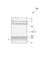
図1は、本実施形態の光電変換装置の構成を示す概略図である。光電変換装置100は、シリコン系太陽電池であり、基板1、基板側透明電極層2、光電変換層3、裏面側透明電極層7、及び裏面電極層4を備える。光電変換層3は、p層41、i層42、n層として窒素含有n層43及び界面処理層44を備える。なお、ここで、シリコン系とはシリコン(Si)やシリコンカーバイト(SiC)やシリコンゲルマニウム(SiGe)を含む総称である。また、結晶質シリコン系とは、非晶質シリコン系以外のシリコン系を意味するものであり、微結晶シリコンや多結晶シリコンも含まれる。
<First Embodiment>
The configuration of the photoelectric conversion device according to the first embodiment of the present invention will be described.
FIG. 1 is a schematic diagram illustrating the configuration of the photoelectric conversion apparatus according to the present embodiment. The
以下に、太陽電池パネルを例に挙げ、第1実施形態に係る光電変換装置の製造方法を、図2から図5を用いて説明する。 Below, a solar cell panel is mentioned as an example and the manufacturing method of the photoelectric conversion apparatus which concerns on 1st Embodiment is demonstrated using FIGS. 2-5.
(1)図2(a):
基板1としてソーダフロートガラス基板(例えば1.4m×1.1m×板厚:3.5mm〜4.5mm)を使用する。基板端面は熱応力や衝撃などによる破損防止にコーナー面取りやR面取り加工されていることが望ましい。
(1) FIG. 2 (a):
A soda float glass substrate (for example, 1.4 m × 1.1 m × plate thickness: 3.5 mm to 4.5 mm) is used as the
(2)図2(b):
基板側透明導電層2として、酸化錫(SnO2)を主成分とする膜厚約500nm以上800nm以下の透明導電膜を、熱CVD装置にて約500℃で製膜する。この際、透明電極膜の表面には、適当な凹凸のあるテクスチャーが形成される。基板側透明導電層2として、透明電極膜に加えて、基板1と透明電極膜との間にアルカリバリア膜(図示されず)を形成しても良い。アルカリバリア膜は、酸化シリコン膜(SiO2)を50nm〜150nm、熱CVD装置にて約500℃で製膜処理する。
(2) FIG. 2 (b):
As the substrate-side transparent
(3)図2(c):
その後、基板1をX−Yテーブルに設置して、YAGレーザーの第1高調波(1064nm)を、図の矢印に示すように、透明電極膜の膜面側から照射する。加工速度に適切となるようにレーザーパワーを調整して、透明電極膜を発電セルの直列接続方向に対して垂直な方向へ、基板1とレーザー光を相対移動して、溝10を形成するように幅約6mmから15mmの所定幅の短冊状にレーザーエッチングする。
(3) FIG. 2 (c):
Thereafter, the
(4)図2(d):
プラズマCVD装置により、基板側透明電極層2上に、太陽光の入射する側から順にp層41、i層42、窒素含有n層43、界面処理層44の順で製膜し、光電変換層3を形成する。
(4) FIG. 2 (d):
Using a plasma CVD apparatus, a p-
p層製膜室に、SiH4ガス、H2ガス、及びB2H6ガスを導入して、減圧雰囲気:3000Pa以下、基板温度:約200℃、プラズマ発生周波数:40MHz以上100MHz以下にて、結晶質シリコンp層41を製膜する。結晶質シリコンp層41はBドープした微結晶シリコンを主とし、膜厚10nm以上50nm以下とされる。
SiH 4 gas, H 2 gas, and B 2 H 6 gas are introduced into the p-layer deposition chamber, and a reduced pressure atmosphere: 3000 Pa or less, a substrate temperature: about 200 ° C., a plasma generation frequency: 40 MHz to 100 MHz, A crystalline
i層製膜室にSiH4ガス及びH2ガスを導入して、減圧雰囲気:3000Pa以下、基板温度:約200℃、プラズマ発生周波数:40MHz以上100MHz以下にて、結晶質シリコンi層42を製膜する。結晶質シリコンi層42は微結晶シリコンを主とし、膜厚は1.2μm以上3.0μm以下とされる。
SiH 4 gas and H 2 gas are introduced into the i-layer deposition chamber, and a crystalline silicon i-
微結晶シリコンを主とするi層膜をプラズマCVD法で形成するにあたり、プラズマ放電電極と基板1の表面との距離dは、3mm以上10mm以下にすることが好ましい。3mmより小さい場合、大型基板に対応する製膜室内の各構成機器精度から距離dを一定に保つことが難しくなるとともに、近過ぎて放電が不安定になる恐れがある。10mmより大きい場合、十分な製膜速度(1nm/s以上)を得難くなるとともに、プラズマの均一性が低下しイオン衝撃により膜質が低下する。
In forming the i-layer film mainly composed of microcrystalline silicon by the plasma CVD method, the distance d between the plasma discharge electrode and the surface of the
窒素含有n層43を製膜する。n層製膜室に、SiH4ガス、H2ガス、PH3ガス及びN2ガスを導入する。このとき、製膜速度を考慮すると、水素希釈率H2/SiH4は100倍程度とすることが好ましい。N2ガスは、N2ガス濃度N2/(N2+SiH4)が14%以上63%以下となる流量で導入する。減圧雰囲気:3000Pa以下、基板温度:約200℃、プラズマ発生周波数:30MHz以上100MHz以下(好ましくは40MHz以上100MHz以下)にて、窒素含有n層43を製膜する。上記条件での製膜により、窒素原子濃度1%以上20%以下、好ましくは8%以上18%以下、かつ、結晶化率0以上3未満の窒素含有n層が形成される。本実施形態において、窒素含有n層43の膜厚は、10nm以上50nm以下とされる。
A nitrogen-containing
次に、界面処理層44を製膜する。界面処理44の製膜は、上記窒素含有n層43と同じ製膜室で行っても良いし、別の製膜室で行っても良い。なお、界面処理層44を窒素含有n層43と同じ製膜室で製膜すれば、製膜パラメータの調整が容易であり、製造に要する時間を大幅に短縮できるので有利である。
例えば、n層製膜室に、SiH4ガス、H2ガス、及びPH3ガスを導入する。減圧雰囲気:3000Pa以下、基板温度:約200℃、プラズマ発生周波数:40MHz以上100MHz以下にて、界面処理層の結晶化率が1以上6以下、好ましくは2.5以上5.5以下となるように水素希釈率を調整して、界面処理層44を製膜する。
Next, the
For example, SiH 4 gas, H 2 gas, and PH 3 gas are introduced into the n-layer deposition chamber. Depressurized atmosphere: 3000 Pa or less, substrate temperature: about 200 ° C., plasma generation frequency: 40 MHz or more and 100 MHz or less, the crystallization rate of the interface treatment layer is 1 or more and 6 or less, preferably 2.5 or more and 5.5 or less. The
水素希釈率が低い条件でn型半導体膜を製膜すると、非晶質と結晶質とが混在した膜となるので、結晶化率が低い。この場合、ダングリングボンドや水素終端された結合種などの欠陥を多く含む膜となるため、導電率が低い。水素希釈率が高い条件でn型半導体膜を製膜すると、結晶化率が高くなり、上記の欠陥が低減されて導電率が向上する。しかし、結晶化率が高くなるほど、核生成密度が大きくなるため、粒子径が小さくなる。粒子径が小さくなると粒界が増加するため、導電率が低下する傾向がある。更に、製膜時間が短い場合(製膜初期)では、水素希釈率が高くなると、膜を形成する効果よりもエッチング効果の方が大きくなり、下層にダメージを与える。 When an n-type semiconductor film is formed under a condition where the hydrogen dilution rate is low, a film in which amorphous and crystalline are mixed is formed, so that the crystallization rate is low. In this case, since the film contains many defects such as dangling bonds and hydrogen-terminated bond species, the conductivity is low. When an n-type semiconductor film is formed under a condition where the hydrogen dilution rate is high, the crystallization rate is increased, the defects are reduced, and the conductivity is improved. However, the higher the crystallization rate, the higher the nucleation density and the smaller the particle size. When the particle diameter is reduced, the grain boundary increases, and the conductivity tends to decrease. Further, when the film formation time is short (initial stage of film formation), if the hydrogen dilution rate is increased, the etching effect becomes larger than the effect of forming the film, and the lower layer is damaged.
図6は、ガラス基板上にシリコン系n型半導体膜を膜厚100nmで堆積し、導電率及び結晶化率を評価した結果である。図6において、横軸はシリコン系n型半導体膜の結晶化率、縦軸は導電率である。結晶化率は、シリコン系n型半導体膜側からレーザー光を照射したときのラマンスペクトルのピーク強度から求めた。
図6に示すように、シリコン系n型半導体層の結晶化率が1以上6以下(領域B)で、導電率1S/cm以上100S/cm以下が得られた。特に、シリコン系n型半導体層の結晶化率が2.5以上5.5以下の範囲において、10S/cm以上100S/cm以下と高い導電率が得られた。また、結晶化率が6を超えると(領域C)、導電率が低下する傾向があった。
このように、界面処理層の結晶化率及び導電率には最適範囲が存在する。すなわち、結晶化率が1以上6以下、好ましくは2.5以上5.5以下のn型半導体膜からなる界面処理層とすることで、n層と裏面側透明電極層とのコンタクト性を改善し、かつ、窒素含有n層へのダメージを低減できる。
FIG. 6 shows the results of depositing a silicon-based n-type semiconductor film with a thickness of 100 nm on a glass substrate and evaluating the conductivity and crystallization rate. In FIG. 6, the horizontal axis represents the crystallization rate of the silicon-based n-type semiconductor film, and the vertical axis represents the conductivity. The crystallization rate was determined from the peak intensity of the Raman spectrum when laser light was irradiated from the silicon-based n-type semiconductor film side.
As shown in FIG. 6, the crystallization rate of the silicon-based n-type semiconductor layer was 1 or more and 6 or less (region B), and the conductivity was 1 S / cm or more and 100 S / cm or less. In particular, high conductivity of 10 S / cm or more and 100 S / cm or less was obtained when the crystallization rate of the silicon-based n-type semiconductor layer was 2.5 or more and 5.5 or less. Further, when the crystallization rate exceeded 6 (region C), the conductivity tended to decrease.
Thus, there is an optimum range for the crystallization rate and conductivity of the interface treatment layer. That is, the contact property between the n layer and the back-side transparent electrode layer is improved by forming an interface treatment layer made of an n-type semiconductor film having a crystallization rate of 1 or more and 6 or less, preferably 2.5 or more and 5.5 or less. In addition, damage to the nitrogen-containing n layer can be reduced.
本実施形態において、界面処理層の膜厚は、1nm以上3nm以下とされる。界面処理層の膜厚が上記範囲内であると、高い導電率が得られシリーズ抵抗が低下する。すなわち、n層と基板側透明電極層とのコンタクト性がより良好となり、形状因子が更に向上する。 In this embodiment, the film thickness of the interface treatment layer is 1 nm or more and 3 nm or less. When the thickness of the interface treatment layer is within the above range, high conductivity is obtained and the series resistance is lowered. That is, the contact property between the n layer and the substrate-side transparent electrode layer becomes better, and the shape factor is further improved.
(5)図2(e)
基板1をX−Yテーブルに設置して、レーザーダイオード励起YAGレーザーの第2高調波(532nm)を、図の矢印に示すように、光電変換層3の膜面側から照射する。パルス発振:10kHzから20kHzとして、加工速度に適切となるようにレーザーパワーを調整して、透明電極層2のレーザーエッチングラインの約100μmから150μmの横側を、溝11を形成するようにレーザーエッチングする。またこのレーザーは基板1側から照射しても良く、この場合は光電変換層3で吸収されたエネルギーで発生する高い蒸気圧を利用して光電変換層3をエッチングできるので、更に安定したレーザーエッチング加工を行うことが可能となる。レーザーエッチングラインの位置は前工程でのエッチングラインと交差しないように位置決め交差を考慮して選定する。
(5) FIG. 2 (e)
The
(6)図3(a)
n層と裏面電極層4との接触抵抗低減と光反射向上を目的に、光電変換層3と裏面電極層4との間に、スパッタリング装置により、膜厚:50nm以上100nm以下のGZO(GaドープZnO)膜からなる裏面側透明電極層を形成する。
次いで、裏面電極層4としてAg膜/Ti膜を、スパッタリング装置により、減圧雰囲気、製膜温度:150℃から200℃にて製膜する。本実施形態では、Ag膜:150nm以上500nm以下、これを保護するものとして防食効果の高いTi膜:10nm以上20nm以下を、この順に積層する。あるいは、裏面電極層4を、25nmから100nmの膜厚を有するAg膜と、15nmから500nmの膜厚を有するAl膜との積層構造としても良い。
(6) FIG. 3 (a)
For the purpose of reducing contact resistance between the n layer and the
Next, an Ag film / Ti film is formed as the
(7)図3(b)
基板1をX−Yテーブルに設置して、レーザーダイオード励起YAGレーザーの第2高調波(532nm)を、図の矢印に示すように、基板1側から照射する。レーザー光が光電変換層3で吸収され、このとき発生する高いガス蒸気圧を利用して、裏面側透明電極層7及び裏面電極層4が爆裂して除去される。パルス発振:1kHz以上10kHz以下として加工速度に適切となるようにレーザーパワーを調整して、透明電極層2のレーザーエッチングラインの250μmから400μmの横側を、溝12を形成するようにレーザーエッチングする。
(7) FIG. 3 (b)
The
(8)図3(c)と図4(a)
発電領域を区分して、基板端周辺の膜端部においてレーザーエッチングによる直列接続部分が短絡し易い影響を除去する。基板1をX−Yテーブルに設置して、レーザーダイオード励起YAGレーザーの第2高調波(532nm)を、基板1側から照射する。レーザー光が透明電極層2と光電変換層3で吸収され、このとき発生する高いガス蒸気圧を利用して裏面電極層4が爆裂して、裏面電極層4/裏面側透明電極層/光電変換層3/基板側透明電極層2が除去される。パルス発振:1kHz以上10kHz以下として加工速度に適切となるようにレーザーパワーを調整して、基板1の端部から5mmから20mmの位置を、図3(c)に示すように、X方向絶縁溝15を形成するようにレーザーエッチングする。なお、図3(c)では、光電変換層3が直列に接続された方向に切断したX方向断面図となっているため、本来であれば絶縁溝15位置には裏面電極層4/裏面側透明電極層/光電変換層3/透明電極層2の膜研磨除去をした周囲膜除去領域14がある状態(図4(a)参照)が表れるべきであるが、基板1の端部への加工の説明の便宜上、この位置にY方向断面を表して形成された絶縁溝をX方向絶縁溝15として説明する。このとき、Y方向絶縁溝は後工程で基板1周囲膜除去領域の膜面研磨除去処理を行うので、設ける必要がない。
(8) FIG. 3 (c) and FIG. 4 (a)
The power generation region is divided to eliminate the influence that the serial connection portion due to laser etching is likely to be short-circuited at the film edge around the substrate edge. The
絶縁溝15は基板1の端より5mmから15mmの位置にてエッチングを終了させることにより、太陽電池パネル端部からの太陽電池モジュール6内部への外部湿分浸入の抑制に、有効な効果を呈するので好ましい。
The insulating
尚、以上までの工程におけるレーザー光はYAGレーザーとしているが、YVO4レーザーやファイバーレーザーなどが同様に使用できるものがある。 In addition, although the laser beam in the above process is made into a YAG laser, there exists what can use a YVO4 laser, a fiber laser, etc. similarly.
(9)図4(a:太陽電池膜面側から見た図、b:受光面の基板側から見た図)
後工程のEVA等を介したバックシート24との健全な接着・シール面を確保するために、基板1周辺(周囲膜除去領域14)の積層膜は、段差があるとともに剥離し易いため、この膜を除去して周囲膜除去領域14を形成する。基板1の端から5〜20mmで基板1の全周囲にわたり膜を除去するにあたり、X方向は前述の図3(c)工程で設けた絶縁溝15よりも基板端側において、Y方向は基板端側部付近の溝10よりも基板端側において、裏面電極層4/裏面側透明電極層/光電変換層3/透明電極層2を、砥石研磨やブラスト研磨などを用いて除去を行う。
研磨屑や砥粒は基板1を洗浄処理して除去した。
(9) FIG. 4 (a: view from the solar cell film side, b: view from the substrate side of the light receiving surface)
Since the laminated film around the substrate 1 (peripheral film removal region 14) has a step and is easy to peel off in order to ensure a sound adhesion / seal surface with the
Polishing debris and abrasive grains were removed by cleaning the
(10)図5(a)(b)
端子箱23の取付け部分はバックシート24に開口貫通窓を設けて集電板を取出す。この開口貫通窓部分には絶縁材を複数層で設置して外部からの湿分などの浸入を抑制する。
直列に並んだ一方端の太陽電池発電セルと、他方端部の太陽電池発電セルとから銅箔を用いて集電して太陽電池パネル裏側の端子箱23の部分から電力が取出せるように処理する。銅箔は各部との短絡を防止するために銅箔幅より広い絶縁シートを配置する。
集電用銅箔などが所定位置に配置された後に、太陽電池モジュール6の全体を覆い、基板1からはみ出さないようにEVA(エチレン酢酸ビニル共重合体)等による接着充填材シートを配置する。
EVAの上に、防水効果の高いバックシート24を設置する。バックシート24は本実施形態では防水防湿効果が高いようにPETシート/AL箔/PETシートの3層構造よりなる。
バックシート24までを所定位置に配置したものを、ラミネータにより減圧雰囲気で内部の脱気を行い約150〜160℃でプレスしながら、EVAを架橋させて密着させる。
(10) FIGS. 5 (a) and 5 (b)
An attachment portion of the
Processing so that power can be taken out from the
After the current collecting copper foil or the like is disposed at a predetermined position, an adhesive filler sheet made of EVA (ethylene vinyl acetate copolymer) or the like is disposed so as to cover the entire
A
The EVA sheet is placed in a predetermined position until the
(11)図5(a)
太陽電池モジュール6の裏側に端子箱23を接着剤で取付ける。
(12)図5(b)
銅箔と端子箱23の出力ケーブルとをハンダ等で接続し、端子箱23の内部を封止剤(ポッティング剤)で充填して密閉する。これで太陽電池パネル50が完成する。
(13)図5(c)
図5(b)までの工程で形成された太陽電池パネル50について発電検査ならびに、所定の性能試験を行う。発電検査は、AM1.5、全天日射基準太陽光(1000W/m2)のソーラシミュレータを用いて行う。
(14)図5(d)
発電検査(図5(c))に前後して、外観検査をはじめ所定の性能検査を行う。
(11) FIG. 5 (a)
The
(12) FIG. 5 (b)
The copper foil and the output cable of the
(13) FIG. 5 (c)
A power generation inspection and a predetermined performance test are performed on the
(14) FIG. 5 (d)
Before and after the power generation inspection (FIG. 5C), a predetermined performance inspection is performed including an appearance inspection.
図7は、N2ガス濃度と窒素含有n層中の窒素原子濃度との関係を示すグラフである。同図において、横軸はN2ガス濃度、縦軸は窒素原子濃度である。窒素含有n層の製膜条件は、水素希釈率100倍、製膜圧力93Pa、製膜温度170℃、高周波周波数60MHz、印加電力15W、膜厚30nmとした。
N2ガスの割合が増加するにつれて膜中の窒素原子濃度が増加した。N2ガス濃度14%以上63%以下で窒素原子濃度が1%以上20%以下となり、多量の窒素原子をn層に含有させることができた。
FIG. 7 is a graph showing the relationship between the N 2 gas concentration and the nitrogen atom concentration in the nitrogen-containing n layer. In the figure, the horizontal axis represents the N 2 gas concentration, and the vertical axis represents the nitrogen atom concentration. The film forming conditions for the nitrogen-containing n layer were as follows:
The nitrogen atom concentration in the film increased as the proportion of N 2 gas increased. When the N 2 gas concentration was 14% or more and 63% or less, the nitrogen atom concentration was 1% or more and 20% or less, and a large amount of nitrogen atoms could be contained in the n layer.
図8は、窒素含有n層中の窒素原子濃度と、窒素含有n層の結晶化率との関係を示すグラフである。同図において、横軸は窒素原子濃度、縦軸は結晶化率である。
n層に窒素を添加しないと高い結晶化率であったが、窒素原子濃度が1%以上の場合は、結晶化率は3未満となった。窒素原子濃度が14%以上で結晶化率が0となり、アモルファス膜となった。
FIG. 8 is a graph showing the relationship between the nitrogen atom concentration in the nitrogen-containing n layer and the crystallization rate of the nitrogen-containing n layer. In the figure, the horizontal axis represents the nitrogen atom concentration, and the vertical axis represents the crystallization rate.
When nitrogen was not added to the n layer, the crystallization rate was high. However, when the nitrogen atom concentration was 1% or more, the crystallization rate was less than 3. When the nitrogen atom concentration was 14% or more, the crystallization rate was 0, and an amorphous film was obtained.
図9は、窒素含有n層中の窒素原子濃度と太陽電池モジュールの開放電圧との関係を示すグラフである。同図において、横軸は窒素原子濃度、縦軸は開放電圧である。p層製膜条件は、水素希釈率100倍、製膜圧力67Pa、製膜温度200℃、高周波周波数100MHz、印加電力75W、膜厚30nmとし、i層製膜条件は、水素希釈率21.4倍、製膜圧力400Pa、製膜温度200℃、高周波周波数100MHz、印加電力30W、膜厚2μmとした。
n層中の窒素原子濃度が1%以上20%以下の太陽電池モジュールでは、窒素を添加しない太陽電池モジュールに比べて、開放電圧が高くなった。特に、窒素原子濃度8%以上18%以下で、開放電圧が0.525V以上となり、窒素原子を含まない場合よりも0.15V以上増大した。窒素原子濃度が20%を超えると、逆に開放電圧は低下した。
FIG. 9 is a graph showing the relationship between the nitrogen atom concentration in the nitrogen-containing n-layer and the open circuit voltage of the solar cell module. In the figure, the horizontal axis represents the nitrogen atom concentration, and the vertical axis represents the open circuit voltage. The p-layer deposition conditions are a hydrogen dilution rate of 100 times, a deposition pressure of 67 Pa, a deposition temperature of 200 ° C., a high-frequency frequency of 100 MHz, an applied power of 75 W, and a film thickness of 30 nm. The i-layer deposition condition is a hydrogen dilution rate of 21.4. The film forming pressure was 400 Pa, the film forming temperature was 200 ° C., the high frequency was 100 MHz, the applied power was 30 W, and the film thickness was 2 μm.
In the solar cell module in which the nitrogen atom concentration in the n layer is 1% or more and 20% or less, the open circuit voltage is higher than that of the solar cell module to which nitrogen is not added. In particular, when the nitrogen atom concentration was 8% or more and 18% or less, the open circuit voltage was 0.525 V or more, which was 0.15 V or more higher than the case where no nitrogen atom was contained. Conversely, when the nitrogen atom concentration exceeded 20%, the open circuit voltage decreased.
窒素含有n層の製膜速度は、結晶化率が高いほど低下する傾向があった。窒素含有n層の結晶化率が3未満であるときの製膜速度は、窒素含有n層の結晶化率が0(非晶質シリコン)であるときの製膜速度の60%以上となった。これは、窒素含有n層の結晶化率が3未満であれば、窒素を添加したn層を製膜しても、生産性低下への影響を抑えられることを意味する。 The deposition rate of the nitrogen-containing n layer tended to decrease as the crystallization rate increased. The film formation rate when the crystallization rate of the nitrogen-containing n layer is less than 3 is 60% or more of the film formation rate when the crystallization rate of the nitrogen-containing n layer is 0 (amorphous silicon). . This means that if the crystallization rate of the nitrogen-containing n layer is less than 3, even if the n layer to which nitrogen is added is formed, the influence on productivity reduction can be suppressed.
表1に、図6における領域A、領域B、領域Cに対応する結晶化率及び導電率を有する界面処理層を形成した太陽電池セルの特性を示す。各太陽電池セルのp層(Bドープ結晶質シリコン)製膜条件は、水素希釈率100倍、製膜圧力67Pa、製膜温度165℃、高周波周波数100MHz、印加電力75W、膜厚30nmとした。各太陽電池セルのi層(結晶質シリコン)製膜条件は、水素希釈率21.4倍、製膜圧力400Pa、製膜温度100℃、高周波周波数100MHz、印加電力30W、膜厚2μmとした。各太陽電池セルの窒素含有n層及び界面処理層の製膜条件は、水素希釈率100倍、製膜圧力93Pa、製膜温度170℃、高周波周波数60MHz、印加電力15Wとした。窒素含有n層の膜厚は、30nm、界面処理層の膜厚は、2nmとした。各界面処理層は、膜厚100nmの場合に表1に示す結晶化率及び導電率が得られる製膜条件にて、所望の界面処理層膜厚が得られる時間で製膜した。

結晶化率1以上6以下の範囲内の結晶質シリコン界面処理層(領域B)を形成した場合、導電率が向上して他の太陽電池セルよりもシリーズ抵抗Rsが低下し、形状因子が大きくなった。その結果、変換効率が上昇した。一方、非晶質シリコン界面処理層(領域A)、及び、結晶化率が6を超える結晶質シリコン界面処理層(領域C)を形成した場合は、導電率が低いためにシリーズ抵抗Rsが大きく、形状因子向上効果が得られなかった。 When a crystalline silicon interface treatment layer (region B) having a crystallization ratio in the range of 1 to 6 is formed, the conductivity is improved, the series resistance Rs is lower than that of other solar cells, and the shape factor is large. became. As a result, the conversion efficiency increased. On the other hand, when the amorphous silicon interface treatment layer (region A) and the crystalline silicon interface treatment layer (region C) having a crystallization rate exceeding 6 are formed, the series resistance Rs is large due to the low conductivity. The effect of improving the shape factor was not obtained.
界面処理層を形成した複数の太陽電池セル、及び、界面処理層が無い複数の太陽電池セルについて、シリーズ抵抗の分布を図10に、形状因子の分布を図11に示す。各層の形成条件は、表1に示す太陽電池セルと同じとした。
図10及び図11から明らかなように、界面処理層を形成した太陽電池セルでは、シリーズ抵抗Rsが低く、ばらつきも抑えられた結果、形状因子を高い値で安定させることができた。これは、高い変換効率の太陽電池セルを安定して得られることを意味する。
FIG. 10 shows the distribution of series resistance and FIG. 11 shows the distribution of form factor for a plurality of solar cells formed with an interface treatment layer and a plurality of solar cells without an interface treatment layer. The conditions for forming each layer were the same as those of the solar battery cell shown in Table 1.
As is apparent from FIGS. 10 and 11, in the solar battery cell in which the interface treatment layer is formed, the series resistance Rs is low and variation is suppressed. As a result, the shape factor can be stabilized at a high value. This means that solar cells with high conversion efficiency can be obtained stably.
界面処理層膜厚と、太陽電池セルのシリーズ抵抗(図12)、形状因子(図13)、開放電圧(図14)、変換効率(図15)との関係を表したグラフを示す。各図における横軸は、界面処理層の膜厚である。縦軸は、図12ではシリーズ抵抗、図13では形状因子、図14では開放電圧、図15では太陽電池セルの変換効率とした。各層の形成条件は、界面処理層の膜厚以外は表1に示す太陽電池セルと同じとした。各図中の横実線は、窒素含有しないn層(界面処理層なし)を形成した従来の太陽電池セルの値を表している。 The graph showing the relationship between an interface treatment layer film thickness, the series resistance (FIG. 12) of a photovoltaic cell, a shape factor (FIG. 13), an open circuit voltage (FIG. 14), and conversion efficiency (FIG. 15) is shown. The horizontal axis in each figure is the film thickness of the interface treatment layer. The vertical axis represents the series resistance in FIG. 12, the form factor in FIG. 13, the open circuit voltage in FIG. 14, and the conversion efficiency of the solar cell in FIG. The formation conditions of each layer were the same as those of the solar battery cell shown in Table 1 except for the film thickness of the interface treatment layer. The horizontal solid line in each figure represents the value of a conventional solar cell in which an n layer not containing nitrogen (no interfacial treatment layer) is formed.
界面処理層が2nmの場合、他の太陽電池セルに比べて、シリーズ抵抗が低下して形状因子が向上した。図12及び図13から、界面処理層が1nm以上3nm以下とした場合に、形状因子向上効果が得られると言える。
開放電圧は、窒素含有n層形成により従来の太陽電池セルよりも大幅に向上した。界面処理層が2nmの太陽電池セルは、従来の太陽電池セル及び界面処理層を形成しない太陽電池セルよりも光電変換効率が向上した。なお、本実験では、界面処理層が5nm及び10nmの場合でも高い変換効率が得られているが、これは図14に示される開放電圧、及び、短絡電流が向上した影響によるものである。
When the interface treatment layer was 2 nm, the series resistance was lowered and the shape factor was improved as compared with other solar cells. From FIG. 12 and FIG. 13, it can be said that when the interface treatment layer is 1 nm or more and 3 nm or less, the effect of improving the shape factor is obtained.
The open-circuit voltage was greatly improved over the conventional solar cell by forming the nitrogen-containing n-layer. The photovoltaic cell having an interface treatment layer of 2 nm has a higher photoelectric conversion efficiency than the conventional photovoltaic cell and the photovoltaic cell not forming the interface treatment layer. In this experiment, high conversion efficiency is obtained even when the interface treatment layer is 5 nm and 10 nm. This is due to the effect of improving the open-circuit voltage and the short-circuit current shown in FIG.
<第2実施形態>
本発明の第2実施形態に係る光電変換装置の構成について説明する。
図16は、第2実施形態の光電変換装置の構成を示す概略図である。光電変換装置100は、タンデム型シリコン系太陽電池である。光電変換層3は、基板1側から順に第1セル層91と第2セル層92とが積層されて構成される。第1セル層91は、太陽光の入射する側から順に、非晶質シリコン薄膜からなるp層31、i層32、n層33を積層して構成される。第2セル層92は、太陽光の入射する側から順に、p層41、i層42、窒素含有n層43、界面処理層44を積層して構成される。第1セル層91と第2セル層92との間に、中間コンタクト層5が設けられる。界面処理層44の太陽光入射側と反対側に、裏面側透明電極層7及び裏面電極層4が順に積層される。
Second Embodiment
The configuration of the photoelectric conversion device according to the second embodiment of the present invention will be described.
FIG. 16 is a schematic diagram illustrating a configuration of a photoelectric conversion apparatus according to the second embodiment. The
以下に、太陽電池パネルを例に挙げて、第2実施形態の光電変換装置における光電変換層の形成工程を説明する。他の太陽電池パネルの製造工程は第1実施形態と略同一であるので説明を省略する。 Below, a solar cell panel is mentioned as an example and the formation process of the photoelectric converting layer in the photoelectric conversion apparatus of 2nd Embodiment is demonstrated. Since the manufacturing process of the other solar cell panel is substantially the same as that of the first embodiment, the description thereof is omitted.
光電変換層3の第1セル層91として、SiH4ガスとH2ガスとを主原料にして、減圧雰囲気:30Pa以上1000Pa以下、基板温度:約200℃、周波数:40MHz以上100MHz以下にて、基板側透明電極層2上に太陽光の入射する側からp層31、i層32、n層33の順で製膜する。p層31は、原料ガスとして更にB2H6ガスを導入して製膜され、膜厚10nm以上30nm以下の非晶質のBドープシリコン膜とする。i層32は、非晶質のシリコン膜であり、膜厚200nm以上350nm以下である。n層33は、原料ガスとして更にPH3を導入して製膜され、膜厚30nm以上50nm以下の非晶質シリコンに微結晶シリコンを含有するPドープシリコンを主とされる。このように、n層33は、窒素を積極的に導入せずに形成される。p層31とi層32の間には、界面特性の向上のためにバッファ層を設けても良い。
As the
本実施形態において、第1セル層91と第2セル層92との間に、接触性を改善するとともに電流整合性を取るために半反射膜となる、中間コンタクト層5を形成する。中間コンタクト層5として、例えば、スパッタリング装置によりGZO(GaドープZnO)膜を膜厚:20nm以上100nm以下で製膜する。
In the present embodiment, an
第1セル層91上に、第1実施形態と同一の工程により結晶質シリコンp層41、結晶質シリコンi層42、窒素含有n層43、界面処理層44を順次製膜する。本実施形態において、窒素含有n層43は、1%以上20%以下、好ましくは8%以上18%以下の原子濃度で窒素を含有し、結晶化率が0以上3未満とされる。窒素含有n層43の膜厚は、10nm以上50nm以下とされる。界面処理層44は、結晶化率が1以上6以下、好ましくは2.5以上5.5以下とされ、導電率が1S/cm以上100S/cm以下、好ましくは10S/cm以上100S/cm以下とされる。界面処理層44の膜厚は、1nm以上3nm以下とされる。
A crystalline
第2実施形態においても、N2ガス濃度と窒素含有n層中の窒素原子濃度との関係、窒素含有n層中の窒素原子濃度と結晶化率との関係、及び、窒素含有n層中の窒素原子濃度と太陽電池モジュールの開放電圧との関係は、それぞれ図7乃至図9に示す第1実施形態と同様の傾向が見られた。 Also in the second embodiment, the relationship between the N 2 gas concentration and the nitrogen atom concentration in the nitrogen-containing n layer, the relationship between the nitrogen atom concentration in the nitrogen-containing n layer and the crystallization rate, and the nitrogen-containing n layer The same tendency as in the first embodiment shown in FIGS. 7 to 9 was observed in the relationship between the nitrogen atom concentration and the open circuit voltage of the solar cell module.
界面処理層を形成した複数の太陽電池セル、及び、界面処理層が無い複数の太陽電池セルについて、シリーズ抵抗の分布を図17に、形状因子の分布を図18に示す。上記の製膜条件にて、p層膜厚8nm、i層膜厚300nm、n層膜厚40nmの第1セル層を製膜した。第2セル層の製膜条件は、第1実施形態と同一とした。
本実施形態においても、界面処理層を形成した太陽電池セルでは、シリーズ抵抗Rsが低く、ばらつきも抑えられた結果、形状因子を高い値で安定させることができた。これは、高い変換効率のタンデム型太陽電池セルを安定して得られることを意味する。
FIG. 17 shows the distribution of series resistance and FIG. 18 shows the distribution of form factor for a plurality of solar cells having an interface treatment layer and a plurality of solar cells without an interface treatment layer. A first cell layer having a p-layer thickness of 8 nm, an i-layer thickness of 300 nm, and an n-layer thickness of 40 nm was formed under the above film-forming conditions. The film forming conditions for the second cell layer were the same as those in the first embodiment.
Also in this embodiment, in the solar cell in which the interface treatment layer is formed, the series resistance Rs is low and the variation is suppressed. As a result, the form factor can be stabilized at a high value. This means that a tandem solar cell with high conversion efficiency can be stably obtained.
界面処理層膜厚と、太陽電池セルのシリーズ抵抗(図19)、形状因子(図20)、開放電圧(図21)、変換効率(図22)との関係を表したグラフを示す。各図における横軸は、界面処理層の膜厚である。縦軸は、図19ではシリーズ抵抗、図20では形状因子、図21では開放電圧、図22では太陽電池セルの変換効率とした。界面処理層の膜厚以外は、各層の条件は図17及び図18の太陽電池セルと同じとした。各図中の横実線は、窒素含有しないn層(界面処理層なし)を形成した従来の太陽電池セルの値を表している。 The graph showing the relationship between the interface treatment layer film thickness, the series resistance (FIG. 19), the shape factor (FIG. 20), the open circuit voltage (FIG. 21), and the conversion efficiency (FIG. 22) of the solar battery cell is shown. The horizontal axis in each figure is the film thickness of the interface treatment layer. The vertical axis represents the series resistance in FIG. 19, the form factor in FIG. 20, the open circuit voltage in FIG. 21, and the conversion efficiency of the solar cells in FIG. Except for the film thickness of the interface treatment layer, the conditions of each layer were the same as those of the solar battery cell of FIGS. The horizontal solid line in each figure represents the value of a conventional solar cell in which an n layer not containing nitrogen (no interfacial treatment layer) is formed.
界面処理層が2nmの場合、他の太陽電池セルに比べて、シリーズ抵抗が低下して形状因子が向上した。図19及び図20から、界面処理層が1nm以上3nm以下とした場合に、形状因子向上効果が得られると言える。開放電圧は、窒素含有n層形成により従来の太陽電池セルよりも大幅に向上した。界面処理層が2nmの太陽電池セルは、従来の太陽電池セル及び界面処理層を形成しない太陽電池セルよりも光電変換効率が向上した。 When the interface treatment layer was 2 nm, the series resistance was lowered and the shape factor was improved as compared with other solar cells. From FIG. 19 and FIG. 20, it can be said that when the interface treatment layer is 1 nm or more and 3 nm or less, the effect of improving the shape factor can be obtained. The open-circuit voltage was greatly improved over the conventional solar cell by forming the nitrogen-containing n-layer. The photovoltaic cell having an interface treatment layer of 2 nm has a higher photoelectric conversion efficiency than the conventional photovoltaic cell and the photovoltaic cell not forming the interface treatment layer.
<第3実施形態>
本発明の第3実施形態に係る光電変換装置の構成について説明する。
図23は、第3実施形態の光電変換装置の構成を示す概略図である。光電変換装置100は、トリプル型シリコン系太陽電池である。光電変換層3は、基板1側から順に第1セル層91、第2セル層92、第3セル層93が積層されて構成される。第1セル層91は、太陽光の入射する側から順に、非晶質シリコン薄膜からなるp層31、i層32、n層33を積層して構成される。第2セル層92は、太陽光の入射する側から順に、p層41、i層42、n層45を積層して構成される。第3セル層93は、太陽光の入射する側から順に、p層61、i層62、窒素含有n層63、界面処理層64を積層して構成される。第1セル層91と第2セル層92との間、及び、第2セル層92と第3セル層93との間に、それぞれ中間コンタクト層5a,5bが設けられる。界面処理層64の太陽光入射側と反対側に、裏面側透明電極層7及び裏面電極層4が順に積層される。
<Third Embodiment>
A configuration of the photoelectric conversion device according to the third embodiment of the present invention will be described.
FIG. 23 is a schematic diagram illustrating a configuration of a photoelectric conversion apparatus according to the third embodiment. The
以下に、太陽電池パネルを例に挙げて、第3実施形態の光電変換装置における光電変換層の形成工程を説明する。他の太陽電池パネルの製造工程は第1実施形態と略同一であるので説明を省略する。 Below, a solar cell panel is mentioned as an example and the formation process of the photoelectric converting layer in the photoelectric conversion apparatus of 3rd Embodiment is demonstrated. Since the manufacturing process of the other solar cell panel is substantially the same as that of the first embodiment, the description thereof is omitted.
第1セル層91として、第2実施形態と同一の工程により、非晶質シリコンp層31、非晶質シリコンi層32、非晶質シリコンに微結晶シリコンを含有するPドープシリコンを主とするn層33を製膜する。本実施形態において、p層31の膜厚は10nm以上30nm以下、i層32の膜厚は200nm以上350nm以下、n層33の膜厚は30nm以上50nm以下とされる。
As the
第2セル層92として、第1実施形態と同一の工程により結晶質シリコンp層41、結晶質シリコンi層42を製膜する。次いで、減圧雰囲気:3000Pa以下、基板温度:約200℃、周波数:30MHz以上100MHz以下にて、結晶質シリコンn層45を製膜する。本実施形態において、p層41の膜厚は10nm以上50nm以下、i層42の膜厚は1.2μm以上3μm以下、n層45の膜厚は10nm以上50nm以下とされる。
As the
第3セル層93として、第1実施形態と同一の工程により、結晶質シリコンp層61を製膜する。次いで、原料ガス:SiH4ガス、GeH4ガス、H2ガスを減圧雰囲気:3000Pa以下、基板温度:約200℃、プラズマ発生周波数:40MHz以上100MHz以下にて、結晶質シリコンゲルマニウムi層62を製膜する。次いで、第1実施形態と同一の窒素含有n層63、界面処理層64を順次製膜する。
第3セル層93のp層61の膜厚は10nm以上50nm以下、i層62の膜厚は1μm以上3μm以下、窒素含有n層63の膜厚は10nm以上50nm以下、界面処理層64の膜厚は1nm以上3nm以下とされる。
As the
The thickness of the
第3実施形態について、N2ガス濃度と窒素含有n層中の窒素原子濃度との関係、窒素含有n層中の窒素原子濃度と結晶化率との関係、及び、窒素含有n層中の窒素原子濃度と太陽電池モジュールの開放電圧との関係は、それぞれ、第1実施形態と同様の傾向が見られた。
本実施形態においても、第1実施形態及び第2実施形態と同様に、窒素含有n層を形成することにより、開放電圧を向上させることができた。また、界面処理層を形成することにより、シリーズ抵抗Rsが低く、ばらつきも抑えられたため、形状因子を高い値で安定させることができた。このように、トリプル型太陽電池セルにおいても、窒素含有n層及び界面処理層の効果が確認された。
Regarding the third embodiment, the relationship between the N 2 gas concentration and the nitrogen atom concentration in the nitrogen-containing n layer, the relationship between the nitrogen atom concentration in the nitrogen-containing n layer and the crystallization rate, and the nitrogen in the nitrogen-containing n layer The same tendency as in the first embodiment was observed in the relationship between the atomic concentration and the open circuit voltage of the solar cell module.
Also in the present embodiment, the open-circuit voltage can be improved by forming the nitrogen-containing n-layer as in the first and second embodiments. Further, by forming the interface treatment layer, the series resistance Rs was low and variation was suppressed, so that the shape factor could be stabilized at a high value. Thus, the effect of the nitrogen-containing n layer and the interface treatment layer was confirmed also in the triple solar cell.
<第4実施形態>
本発明の第4実施形態に係る光電変換装置の構成について説明する。
図24は、第4実施形態の光電変換装置の構成を示す概略図である。光電変換装置100は、トリプル型シリコン系太陽電池である。光電変換層3は、基板1側から順に第1セル層91、第2セル層92、第3セル層93が積層されて構成される。第1セル層91は、太陽光の入射する側から順に、非晶質シリコン薄膜からなるp層31、i層32、n層33を積層して構成される。第2セル層92は、太陽光の入射する側から順に、p層41、i層42、窒素含有n層43、界面処理層44を積層して構成される。第3セル層93は、太陽光の入射する側から順に、p層61、i層62、n層65を積層して構成される。第1セル層91と第2セル層92との間、及び、第2セル層92と第3セル層93との間に、それぞれ中間コンタクト層5a,5bが設けられる。第3セル層のn層65の太陽光入射側と反対側に、裏面側透明電極層7及び裏面電極層4が順に積層される。
<Fourth embodiment>
A configuration of the photoelectric conversion device according to the fourth embodiment of the present invention will be described.
FIG. 24 is a schematic diagram illustrating a configuration of a photoelectric conversion apparatus according to the fourth embodiment. The
以下に、太陽電池パネルを例に挙げて、第4実施形態の光電変換装置における光電変換層の形成工程を説明する。他の太陽電池パネルの製造工程は第1実施形態と略同一であるので説明を省略する。 Below, a solar cell panel is mentioned as an example and the formation process of the photoelectric converting layer in the photoelectric conversion apparatus of 4th Embodiment is demonstrated. Since the manufacturing process of the other solar cell panel is substantially the same as that of the first embodiment, the description thereof is omitted.
第1セル層91は、第3実施形態と同様にして形成される。
第2セル層92として、第2実施形態と同一の工程で、結晶質シリコンp層41、結晶質シリコンi層42、窒素含有n層43、界面処理層44を順次製膜する。本実施形態において、p層41の膜厚は10nm以上50nm以下、i層42の膜厚は1.2μm以上3μm以下、窒素含有n層43の膜厚は10nm以上50nm以下、界面処理層44の膜厚は1nm以上3nm以下とされる。
The
As the
第3実施形態の第2セル層と同様の工程により、第3セル層93を形成する。本実施形態において、p層61の膜厚は10nm以上50nm以下、i層62の膜厚は1μm以上3μm以下、n層65の膜厚は10nm以上50nm以下とされる。
The
第4実施形態においても、N2ガス濃度と窒素含有n層中の窒素原子濃度との関係、窒素含有n層中の窒素原子濃度と結晶化率との関係、及び、窒素含有n層中の窒素原子濃度と太陽電池モジュールの開放電圧との関係は、それぞれ、第1実施形態と同様の傾向が見られた。 Also in the fourth embodiment, the relationship between the N 2 gas concentration and the nitrogen atom concentration in the nitrogen-containing n layer, the relationship between the nitrogen atom concentration in the nitrogen-containing n layer and the crystallization rate, and the nitrogen-containing n layer A tendency similar to that in the first embodiment was observed between the nitrogen atom concentration and the open circuit voltage of the solar cell module.
界面処理層を形成した複数の太陽電池セル、及び、界面処理層が無い複数の太陽電池セルについて、シリーズ抵抗の分布を図25に、形状因子の分布を図26に示す。上記の製膜条件にて、第1セル層のp層膜厚を8nm、i層膜厚を300nm、n層膜厚を40nmとした。第2セル層の製膜条件は、第1実施形態と同一とした。第3セル層のp層膜厚を30nm、i層膜厚を2μm、n層膜厚を30nmとした。
本実施形態においても、界面処理層を形成した太陽電池セルでは、シリーズ抵抗Rsが低く、ばらつきも抑えられた結果、形状因子を高い値で安定させることができた。これは、高い変換効率のトリプル型太陽電池セルを安定して得られることを意味する。
FIG. 25 shows the distribution of series resistance and FIG. 26 shows the distribution of form factor for a plurality of solar cells with an interface treatment layer and a plurality of solar cells without an interface treatment layer. Under the above film forming conditions, the p-layer thickness of the first cell layer was 8 nm, the i-layer thickness was 300 nm, and the n-layer thickness was 40 nm. The film forming conditions for the second cell layer were the same as those in the first embodiment. The p-layer thickness of the third cell layer was 30 nm, the i-layer thickness was 2 μm, and the n-layer thickness was 30 nm.
Also in this embodiment, in the solar cell in which the interface treatment layer is formed, the series resistance Rs is low and the variation is suppressed. As a result, the form factor can be stabilized at a high value. This means that a high conversion efficiency triple solar cell can be obtained stably.
界面処理層膜厚と、太陽電池セルのシリーズ抵抗(図27)、形状因子(図28)、開放電圧(図29)、変換効率(図30)との関係を表したグラフを示す。各図における横軸は、界面処理層の膜厚である。縦軸は、図27ではシリーズ抵抗、図28では形状因子、図29では開放電圧、図30では太陽電池セルの変換効率とした。界面処理層の膜厚以外は、各層の条件は、図25及び図26の太陽電池セルと同じとした。各図中の横実線は、窒素を含有しないn層(界面処理層なし)を形成した従来の太陽電池セルの値を表している。 The graph showing the relationship between the interface treatment layer film thickness, the series resistance (FIG. 27), the form factor (FIG. 28), the open circuit voltage (FIG. 29), and the conversion efficiency (FIG. 30) of the solar battery cell is shown. The horizontal axis in each figure is the film thickness of the interface treatment layer. The vertical axis represents the series resistance in FIG. 27, the shape factor in FIG. 28, the open circuit voltage in FIG. 29, and the conversion efficiency of the solar cells in FIG. Except for the film thickness of the interface treatment layer, the conditions of each layer were the same as those of the solar battery cell of FIGS. The horizontal solid line in each figure represents the value of a conventional solar cell in which an n layer not containing nitrogen (no interfacial treatment layer) is formed.
界面処理層が2nmの場合、シリーズ抵抗が低下して形状因子が向上した。開放電圧は、窒素含有n層形成により従来の太陽電池セルよりも大幅に向上した。界面処理層が2nmの太陽電池セルは、従来の太陽電池セル及び界面処理層を形成しない太陽電池セルよりも光電変換効率が向上した。図27及び図28から、界面処理層が1nm以上3nm以下とした場合に、形状因子向上効果が得られると言える。
以上のように、窒素含有n層と中間コンタクト層との間に界面処理層を形成した場合でも、窒素含有n層による開放電圧向上効果、及び、界面処理層によるコンタクト性改善による形状因子向上効果を得ることができた。
When the interface treatment layer was 2 nm, the series resistance was lowered and the shape factor was improved. The open-circuit voltage was greatly improved over the conventional solar cell by forming the nitrogen-containing n-layer. The photovoltaic cell having an interface treatment layer of 2 nm has a higher photoelectric conversion efficiency than the conventional photovoltaic cell and the photovoltaic cell not forming the interface treatment layer. From FIG. 27 and FIG. 28, it can be said that when the interface treatment layer is 1 nm or more and 3 nm or less, the effect of improving the shape factor is obtained.
As described above, even when an interface treatment layer is formed between the nitrogen-containing n layer and the intermediate contact layer, the open-circuit voltage improvement effect by the nitrogen-containing n layer and the form factor improvement effect by the contact property improvement by the interface treatment layer Could get.
1 基板
2 基板側透明電極層
3 光電変換層
4 裏面電極層
5,5a,5b 中間コンタクト層
6 太陽電池モジュール
7 裏面側透明電極層
31,41,61 p層
32,42,62 i層
33,45,65 n層
43,63 窒素含有n層
44,64 界面処理層
91 第1セル層
92 第2セル層
93 第3セル層
100 光電変換装置
DESCRIPTION OF
Claims (8)
前記n層が、窒素含有n層と、該窒素含有n層の前記基板と反対側の面に形成された界面処理層とを備え、
前記窒素含有n層が、窒素原子を1%以上20%以下の原子濃度で含有し、かつ、結晶化率が0以上3未満であり、
前記界面処理層が、GaドープZnOからなる裏面側の透明電極層と接触し、
前記界面処理層が、結晶化率1以上6以下であり、
前記界面処理層の導電率が、1S/cm以上100S/cm以下であることを特徴とする光電変換装置。 A photoelectric conversion device including a silicon-based photoelectric conversion layer in which a p layer, an i layer, and an n layer are stacked on a substrate,
The n layer includes a nitrogen-containing n layer and an interface treatment layer formed on the surface of the nitrogen-containing n layer opposite to the substrate,
The nitrogen-containing n layer contains nitrogen atoms at an atomic concentration of 1% or more and 20% or less, and the crystallization rate is 0 or more and less than 3.
The interface treatment layer is in contact with a transparent electrode layer on the back side made of Ga-doped ZnO ,
The interface treatment layer has a crystallization ratio of 1 to 6,
An electrical conductivity of the interface treatment layer is 1 S / cm or more and 100 S / cm or less.
前記n層が、窒素含有n層と、該窒素含有n層の前記基板と反対側の面に形成された界面処理層とを備え、
前記窒素含有n層が、窒素原子を1%以上20%以下の原子濃度で含有し、かつ、結晶化率が0以上3未満であり、
隣接する前記光電変換層の間に、隣接する前記光電変換層同士を電気的に接続し、且つ、光を透過するGaドープZnOからなる中間コンタクト層を備え、
前記界面処理層が、前記中間コンタクト層と接触し、
前記界面処理層が、結晶化率1以上6以下であり、
前記界面処理層の導電率が、1S/cm以上100S/cm以下であることを特徴とする光電変換装置。 A photoelectric conversion device including a plurality of silicon-based photoelectric conversion layers in which a p layer, an i layer, and an n layer are stacked on a substrate,
The n layer includes a nitrogen-containing n layer and an interface treatment layer formed on the surface of the nitrogen-containing n layer opposite to the substrate,
The nitrogen-containing n layer contains nitrogen atoms at an atomic concentration of 1% or more and 20% or less, and the crystallization rate is 0 or more and less than 3.
An intermediate contact layer made of Ga-doped ZnO that electrically connects adjacent photoelectric conversion layers and transmits light between the adjacent photoelectric conversion layers ,
The interface treatment layer is in contact with the intermediate contact layer;
The interface treatment layer has a crystallization ratio of 1 to 6,
An electrical conductivity of the interface treatment layer is 1 S / cm or more and 100 S / cm or less.
前記界面処理層の導電率が、10S/cm以上100S/cm以下であることを特徴とする請求項1または請求項2に記載の光電変換装置。 The crystallization ratio of the interface treatment layer is 2.5 or more and 5.5 or less,
3. The photoelectric conversion device according to claim 1, wherein an electrical conductivity of the interface treatment layer is 10 S / cm or more and 100 S / cm or less.
前記n層を形成する工程が、窒素原子濃度が1%以上20%以下、かつ、結晶化率が0以上3未満の窒素含有n層を、原料ガスに窒素ガスを用い、30MHz以上100MHz以下の高周波周波数で、高周波プラズマCVD法によって形成する工程と、該窒素含有n層の前記基板と反対側の面に、結晶化率1以上6以下の界面処理層を、導電率が1S/cm以上100S/cm以下として形成する工程と、
前記界面処理層上に、GaドープZnOからなる裏面側の透明電極層を形成する工程と、
を含むことを特徴とする光電変換装置の製造方法。 A method of manufacturing a photoelectric conversion device including a step of forming a silicon-based photoelectric conversion layer in which a p layer, an i layer, and an n layer are stacked on a substrate,
In the step of forming the n layer, a nitrogen-containing n layer having a nitrogen atom concentration of 1% or more and 20% or less and a crystallization rate of 0 or more and less than 3 is used. A step of forming at a high frequency by a high frequency plasma CVD method, and an interface treatment layer having a crystallization ratio of 1 to 6 on the surface of the nitrogen-containing n layer opposite to the substrate, having an electrical conductivity of 1 S / cm to 100 S. / Cm or less forming step ,
Forming a backside transparent electrode layer made of Ga-doped ZnO on the interface treatment layer;
A process for producing a photoelectric conversion device comprising:
前記n層を形成する工程が、窒素原子濃度が1%以上20%以下、かつ、結晶化率が0以上3未満の窒素含有n層を、原料ガスに窒素ガスを用い、30MHz以上100MHz以下の高周波周波数で、高周波プラズマCVD法によって形成する工程と、該窒素含有n層の前記基板と反対側の面に、結晶化率1以上6以下の界面処理層を、導電率が1S/cm以上100S/cm以下として形成する工程と、
隣接する前記光電変換層の間の前記界面処理層上に、隣接する前記光電変換層同士を電気的に接続し、且つ、光を透過するGaドープZnOからなる中間コンタクト層を形成する工程を含むことを特徴とする光電変換装置の製造方法。 A method of manufacturing a photoelectric conversion device including a step of forming a plurality of silicon-based photoelectric conversion layers in which a p layer, an i layer, and an n layer are stacked on a substrate,
In the step of forming the n layer, a nitrogen-containing n layer having a nitrogen atom concentration of 1% or more and 20% or less and a crystallization rate of 0 or more and less than 3 is used. A step of forming at a high frequency by a high frequency plasma CVD method, and an interface treatment layer having a crystallization ratio of 1 to 6 on the surface of the nitrogen-containing n layer opposite to the substrate, having an electrical conductivity of 1 S / cm to 100 S. / Cm or less forming step,
Forming an intermediate contact layer made of Ga-doped ZnO that electrically connects adjacent photoelectric conversion layers and transmits light on the interface treatment layer between the adjacent photoelectric conversion layers ; process for producing a photovoltaic device you wherein a.
Priority Applications (7)
| Application Number | Priority Date | Filing Date | Title |
|---|---|---|---|
| JP2008282096A JP4764469B2 (en) | 2008-10-31 | 2008-10-31 | Photoelectric conversion device and method of manufacturing photoelectric conversion device |
| PCT/JP2009/062429 WO2010050271A1 (en) | 2008-10-31 | 2009-07-08 | Photoelectric conversion device and method for manufacturing photoelectric conversion device |
| US12/997,418 US8859887B2 (en) | 2008-10-31 | 2009-07-08 | Photovoltaic device and process for producing photovoltaic device |
| KR1020107028750A KR20110020852A (en) | 2008-10-31 | 2009-07-08 | Photoelectric conversion device and manufacturing method of the photoelectric conversion device |
| CN2009801239407A CN102067325B (en) | 2008-10-31 | 2009-07-08 | Photoelectric conversion device and method for manufacturing photoelectric conversion device |
| EP09823384A EP2343741A1 (en) | 2008-10-31 | 2009-07-08 | Photoelectric conversion device and method for manufacturing photoelectric conversion device |
| TW098127747A TWI435453B (en) | 2008-10-31 | 2009-08-18 | A photoelectric conversion device, and a method of manufacturing the photoelectric conversion device |
Applications Claiming Priority (1)
| Application Number | Priority Date | Filing Date | Title |
|---|---|---|---|
| JP2008282096A JP4764469B2 (en) | 2008-10-31 | 2008-10-31 | Photoelectric conversion device and method of manufacturing photoelectric conversion device |
Publications (2)
| Publication Number | Publication Date |
|---|---|
| JP2010109279A JP2010109279A (en) | 2010-05-13 |
| JP4764469B2 true JP4764469B2 (en) | 2011-09-07 |
Family
ID=42128641
Family Applications (1)
| Application Number | Title | Priority Date | Filing Date |
|---|---|---|---|
| JP2008282096A Expired - Fee Related JP4764469B2 (en) | 2008-10-31 | 2008-10-31 | Photoelectric conversion device and method of manufacturing photoelectric conversion device |
Country Status (7)
| Country | Link |
|---|---|
| US (1) | US8859887B2 (en) |
| EP (1) | EP2343741A1 (en) |
| JP (1) | JP4764469B2 (en) |
| KR (1) | KR20110020852A (en) |
| CN (1) | CN102067325B (en) |
| TW (1) | TWI435453B (en) |
| WO (1) | WO2010050271A1 (en) |
Families Citing this family (5)
| Publication number | Priority date | Publication date | Assignee | Title |
|---|---|---|---|---|
| WO2012144420A1 (en) * | 2011-04-22 | 2012-10-26 | 国立大学法人東京工業大学 | Silicon solar cell and manufacturing method for same |
| US10371468B2 (en) | 2011-11-30 | 2019-08-06 | Palo Alto Research Center Incorporated | Co-extruded microchannel heat pipes |
| US9120190B2 (en) | 2011-11-30 | 2015-09-01 | Palo Alto Research Center Incorporated | Co-extruded microchannel heat pipes |
| US20130206220A1 (en) * | 2012-02-10 | 2013-08-15 | Palo Alto Research Center Incorporated | Method For Generating Gridlines On Non-Square Substrates |
| CN110400813A (en) * | 2019-07-30 | 2019-11-01 | 深圳大学 | An X-ray digital image detector based on perovskite material |
Family Cites Families (28)
| Publication number | Priority date | Publication date | Assignee | Title |
|---|---|---|---|---|
| US4342044A (en) * | 1978-03-08 | 1982-07-27 | Energy Conversion Devices, Inc. | Method for optimizing photoresponsive amorphous alloys and devices |
| US4492810A (en) * | 1978-03-08 | 1985-01-08 | Sovonics Solar Systems | Optimized doped and band gap adjusted photoresponsive amorphous alloys and devices |
| US4492743A (en) * | 1982-10-15 | 1985-01-08 | Standard Oil Company (Indiana) | Multilayer photoelectrodes and photovoltaic cells |
| JPS60154521A (en) * | 1984-01-23 | 1985-08-14 | Semiconductor Energy Lab Co Ltd | Manufacture of silicon carbide film |
| JP2626653B2 (en) | 1984-03-16 | 1997-07-02 | 株式会社半導体エネルギー研究所 | Silicon semiconductor device |
| JPS6235680A (en) * | 1985-08-09 | 1987-02-16 | Toa Nenryo Kogyo Kk | Amorphous silicon solar battery and manufacture of the same |
| JPH032610A (en) | 1989-05-31 | 1991-01-09 | Tokyo Electric Co Ltd | Position detecting apparatus |
| JP2624577B2 (en) | 1990-12-26 | 1997-06-25 | キヤノン株式会社 | Solar cell and method of manufacturing the same |
| JP2951146B2 (en) * | 1992-04-15 | 1999-09-20 | キヤノン株式会社 | Photovoltaic devices |
| JP2761156B2 (en) * | 1992-06-30 | 1998-06-04 | キヤノン株式会社 | Photovoltaic element, method of manufacturing the same, and power generator using the same |
| CA2102948C (en) * | 1992-11-16 | 1998-10-27 | Keishi Saito | Photoelectric conversion element and power generation system using the same |
| US5716480A (en) * | 1995-07-13 | 1998-02-10 | Canon Kabushiki Kaisha | Photovoltaic device and method of manufacturing the same |
| EP0831538A3 (en) * | 1996-09-19 | 1999-07-14 | Canon Kabushiki Kaisha | Photovoltaic element having a specific doped layer |
| US6211454B1 (en) * | 1998-01-23 | 2001-04-03 | Canon Kabushiki Kaisha | Photovoltaic element |
| JP4208281B2 (en) * | 1998-02-26 | 2009-01-14 | キヤノン株式会社 | Multilayer photovoltaic device |
| US6566594B2 (en) * | 2000-04-05 | 2003-05-20 | Tdk Corporation | Photovoltaic element |
| JP4032610B2 (en) | 2000-06-16 | 2008-01-16 | 富士電機アドバンストテクノロジー株式会社 | Non-single crystal thin film solar cell manufacturing method |
| JP4560245B2 (en) | 2001-06-29 | 2010-10-13 | キヤノン株式会社 | Photovoltaic element |
| JP2003158078A (en) | 2001-11-20 | 2003-05-30 | Mitsubishi Heavy Ind Ltd | Method for forming silicon semiconductor |
| JP3805279B2 (en) | 2002-05-29 | 2006-08-02 | 京セラ株式会社 | Cat-PECVD apparatus and film processing system having the same |
| JP2004128110A (en) | 2002-10-01 | 2004-04-22 | Fuji Electric Holdings Co Ltd | Manufacturing method of thin film solar cell |
| JP4215697B2 (en) | 2004-09-03 | 2009-01-28 | シャープ株式会社 | Photoelectric conversion device and manufacturing method thereof |
| JP4441377B2 (en) | 2004-10-22 | 2010-03-31 | シャープ株式会社 | Photoelectric conversion device and manufacturing method thereof |
| JP4441298B2 (en) | 2004-03-24 | 2010-03-31 | シャープ株式会社 | Photoelectric conversion device and manufacturing method thereof |
| JP4215694B2 (en) | 2004-08-23 | 2009-01-28 | シャープ株式会社 | Photoelectric conversion device and manufacturing method thereof |
| CN101246929A (en) | 2007-02-14 | 2008-08-20 | 北京行者多媒体科技有限公司 | Production of multi-knot thin film photovoltaic device |
| JP2009158667A (en) | 2007-12-26 | 2009-07-16 | Mitsubishi Heavy Ind Ltd | Photoelectric conversion device and manufacturing method thereof |
| US8088641B2 (en) * | 2008-10-30 | 2012-01-03 | Mitsubishi Heavy Industries, Ltd. | Process for producing photovoltaic device |
-
2008
- 2008-10-31 JP JP2008282096A patent/JP4764469B2/en not_active Expired - Fee Related
-
2009
- 2009-07-08 US US12/997,418 patent/US8859887B2/en not_active Expired - Fee Related
- 2009-07-08 CN CN2009801239407A patent/CN102067325B/en not_active Expired - Fee Related
- 2009-07-08 WO PCT/JP2009/062429 patent/WO2010050271A1/en active Application Filing
- 2009-07-08 KR KR1020107028750A patent/KR20110020852A/en not_active Application Discontinuation
- 2009-07-08 EP EP09823384A patent/EP2343741A1/en not_active Withdrawn
- 2009-08-18 TW TW098127747A patent/TWI435453B/en active
Also Published As
| Publication number | Publication date |
|---|---|
| EP2343741A1 (en) | 2011-07-13 |
| CN102067325B (en) | 2013-05-01 |
| TW201017902A (en) | 2010-05-01 |
| TWI435453B (en) | 2014-04-21 |
| WO2010050271A1 (en) | 2010-05-06 |
| JP2010109279A (en) | 2010-05-13 |
| CN102067325A (en) | 2011-05-18 |
| KR20110020852A (en) | 2011-03-03 |
| US20110100444A1 (en) | 2011-05-05 |
| US8859887B2 (en) | 2014-10-14 |
Similar Documents
| Publication | Publication Date | Title |
|---|---|---|
| JP5330723B2 (en) | Photoelectric conversion device | |
| JP4764469B2 (en) | Photoelectric conversion device and method of manufacturing photoelectric conversion device | |
| WO2010052953A1 (en) | Photoelectric conversion device manufacturing method and photoelectric conversion device | |
| WO2010050035A1 (en) | Process for producing photoelectric conversion apparatus | |
| JP5308225B2 (en) | Photoelectric conversion device and manufacturing method thereof | |
| WO2011070805A1 (en) | Process for production of photoelectric conversion device | |
| CN101755340B (en) | Photoelectric converting device and process for producing the photoelectric converting device | |
| WO2010064455A1 (en) | Photoelectric conversion device | |
| JP4875566B2 (en) | Method for manufacturing photoelectric conversion device | |
| CN102105992B (en) | Method for producing photoelectric conversion device | |
| JP5324966B2 (en) | Photoelectric conversion device manufacturing method and film forming device | |
| JP5308226B2 (en) | Photoelectric conversion device and manufacturing method thereof | |
| JP2010251424A (en) | Photoelectric conversion device | |
| JP2008251914A (en) | Multijunction photoelectric converter | |
| JP2010118695A (en) | Photoelectric conversion apparatus, and method of manufacturing the same | |
| JP2011096848A (en) | Method of manufacturing photoelectric conversion device | |
| JP2011077380A (en) | Photoelectric conversion device |
Legal Events
| Date | Code | Title | Description |
|---|---|---|---|
| A02 | Decision of refusal |
Free format text: JAPANESE INTERMEDIATE CODE: A02 Effective date: 20091020 |
|
| A912 | Re-examination (zenchi) completed and case transferred to appeal board |
Free format text: JAPANESE INTERMEDIATE CODE: A912 Effective date: 20100219 |
|
| A521 | Request for written amendment filed |
Free format text: JAPANESE INTERMEDIATE CODE: A523 Effective date: 20110318 |
|
| A521 | Request for written amendment filed |
Free format text: JAPANESE INTERMEDIATE CODE: A523 Effective date: 20110422 |
|
| A01 | Written decision to grant a patent or to grant a registration (utility model) |
Free format text: JAPANESE INTERMEDIATE CODE: A01 |
|
| A61 | First payment of annual fees (during grant procedure) |
Free format text: JAPANESE INTERMEDIATE CODE: A61 Effective date: 20110610 |
|
| FPAY | Renewal fee payment (event date is renewal date of database) |
Free format text: PAYMENT UNTIL: 20140617 Year of fee payment: 3 |
|
| FPAY | Renewal fee payment (event date is renewal date of database) |
Free format text: PAYMENT UNTIL: 20140617 Year of fee payment: 3 |
|
| LAPS | Cancellation because of no payment of annual fees |