JP4721776B2 - Semiconductor memory device - Google Patents
Semiconductor memory device Download PDFInfo
- Publication number
- JP4721776B2 JP4721776B2 JP2005157121A JP2005157121A JP4721776B2 JP 4721776 B2 JP4721776 B2 JP 4721776B2 JP 2005157121 A JP2005157121 A JP 2005157121A JP 2005157121 A JP2005157121 A JP 2005157121A JP 4721776 B2 JP4721776 B2 JP 4721776B2
- Authority
- JP
- Japan
- Prior art keywords
- data
- circuit
- column
- signal
- data line
- Prior art date
- Legal status (The legal status is an assumption and is not a legal conclusion. Google has not performed a legal analysis and makes no representation as to the accuracy of the status listed.)
- Expired - Fee Related
Links
Images


Classifications
-
- G—PHYSICS
- G11—INFORMATION STORAGE
- G11C—STATIC STORES
- G11C11/00—Digital stores characterised by the use of particular electric or magnetic storage elements; Storage elements therefor
- G11C11/21—Digital stores characterised by the use of particular electric or magnetic storage elements; Storage elements therefor using electric elements
- G11C11/34—Digital stores characterised by the use of particular electric or magnetic storage elements; Storage elements therefor using electric elements using semiconductor devices
- G11C11/40—Digital stores characterised by the use of particular electric or magnetic storage elements; Storage elements therefor using electric elements using semiconductor devices using transistors
- G11C11/41—Digital stores characterised by the use of particular electric or magnetic storage elements; Storage elements therefor using electric elements using semiconductor devices using transistors forming static cells with positive feedback, i.e. cells not needing refreshing or charge regeneration, e.g. bistable multivibrator or Schmitt trigger
- G11C11/413—Auxiliary circuits, e.g. for addressing, decoding, driving, writing, sensing, timing or power reduction
-
- G—PHYSICS
- G11—INFORMATION STORAGE
- G11C—STATIC STORES
- G11C7/00—Arrangements for writing information into, or reading information out from, a digital store
- G11C7/10—Input/output [I/O] data interface arrangements, e.g. I/O data control circuits, I/O data buffers
- G11C7/1051—Data output circuits, e.g. read-out amplifiers, data output buffers, data output registers, data output level conversion circuits
- G11C7/1066—Output synchronization
-
- G—PHYSICS
- G11—INFORMATION STORAGE
- G11C—STATIC STORES
- G11C7/00—Arrangements for writing information into, or reading information out from, a digital store
- G11C7/10—Input/output [I/O] data interface arrangements, e.g. I/O data control circuits, I/O data buffers
- G11C7/1051—Data output circuits, e.g. read-out amplifiers, data output buffers, data output registers, data output level conversion circuits
- G11C7/1069—I/O lines read out arrangements
-
- G—PHYSICS
- G11—INFORMATION STORAGE
- G11C—STATIC STORES
- G11C7/00—Arrangements for writing information into, or reading information out from, a digital store
- G11C7/10—Input/output [I/O] data interface arrangements, e.g. I/O data control circuits, I/O data buffers
- G11C7/1078—Data input circuits, e.g. write amplifiers, data input buffers, data input registers, data input level conversion circuits
- G11C7/1096—Write circuits, e.g. I/O line write drivers
-
- G—PHYSICS
- G11—INFORMATION STORAGE
- G11C—STATIC STORES
- G11C2207/00—Indexing scheme relating to arrangements for writing information into, or reading information out from, a digital store
- G11C2207/005—Transfer gates, i.e. gates coupling the sense amplifier output to data lines, I/O lines or global bit lines
Landscapes
- Engineering & Computer Science (AREA)
- Microelectronics & Electronic Packaging (AREA)
- Computer Hardware Design (AREA)
- Static Random-Access Memory (AREA)
- Dram (AREA)
Description
この発明は、半導体記憶装置に関し、特に、スタティック型半導体記憶装置(SRAM:スタティック・ランダム・アクセス・メモリ)に関する。より特定的には、この発明は、SRAMの内部データ読出部の構成および内部データ転送部の構成に関する。 The present invention relates to a semiconductor memory device, and more particularly, to a static semiconductor memory device (SRAM: Static Random Access Memory). More specifically, the present invention relates to the configuration of the internal data reading unit and the configuration of the internal data transfer unit of the SRAM.
SRAMは、メモリセルがラッチ回路で構成されており、相補データが、メモリセル内部の記憶ノードに保持される。したがって、SRAMセルは、電源が供給されている間、安定にデータを記憶することができ、DRAM(ダイナミック・ランダム・アクセス・メモリ)のようにキャパシタの充電電荷で情報を記憶する構成と異なり、記憶データのリフレッシュを行なうことは要求されない。したがって、SRAMは、DRAMに比べて、制御が容易であり、各種処理システムにおいて広く用いられている。 In the SRAM, a memory cell is configured by a latch circuit, and complementary data is held in a storage node inside the memory cell. Therefore, the SRAM cell can stably store data while the power is supplied, and unlike the configuration in which information is stored by the charge of the capacitor as in DRAM (dynamic random access memory), It is not required to refresh the stored data. Therefore, SRAM is easier to control than DRAM and is widely used in various processing systems.
また、SRAMは、行および列(ワード線およびビット線)を同時に選択しても、メモリセルデータは正確に読出されるため、DRAMに比べて高速アクセスが可能であり、サイクル時間が短く、キャッシュメモリなどの高速メモリとして広く利用されている。 In addition, even when a row and a column (word line and bit line) are selected at the same time, the SRAM can read memory cell data accurately, so that it can be accessed at a higher speed than a DRAM, has a short cycle time, and cache. It is widely used as a high-speed memory such as a memory.
このようなSRAMを始めとする各種メモリに対しても、近年の処理システムの高速化に伴ってさらに高速アクセスを実現することが要求される。このような半導体記憶装置の高速化を実現する構成の一例が、特許文献1(特開平6−333389号公報)において示されている。 With respect to various memories such as SRAM as well, it is required to realize higher-speed access with the recent increase in processing system speed. An example of a configuration for realizing the high speed of such a semiconductor memory device is shown in Patent Document 1 (Japanese Patent Laid-Open No. 6-333389).
この特許文献1は、DRAMのデータ読出を高速化する構成を示している。すなわち、特許文献1に示される構成においては、選択列を共通データ線に接続する列選択ゲートの相互コンダクタンスgmを増大させるために、列選択信号の電圧レベルを、内部電源電圧よりも高いレベルに昇圧し、低抵抗で選択列のビット線(センスアンプ)を共通データ線に結合する。
This
この特許文献1に示される構成においては、またメモリアレイは、ビット線を分割するようにブロック分割構造に形成され、分割ビット線の間にセンスアンプが配置され、いわゆる「シェアードセンスアンプ」構成が用いられる。ビット線の負荷を軽減して、センスアンプに対するメモリセルの読出電圧を増大し、また高速でセンスアンプにメモリセルデータを転送することにより、高速読出を実現することを図る。
In the configuration shown in
また、SRAMのデータ読出部のセンスアンプを高速化することを意図する構成が、特許文献2(特開平6−119785号公報)に示されている。この特許文献2に示される構成においては、内部データ線へ、選択列のビット線対が結合される。この内部データ線上の信号変化を、カレントミラー型センスアンプで検出する。特許文献2は、このセンスアンプの読出信号波形を対称波形とするために、2段のカレントミラー型センスアンプを設け、初段のセンスアンプにおいて内部データ線対の相補信号に従って相補なミラー電流を生成し、この相補ミラー電流により次段センスアンプを駆動して、メインアンプまたは出力バッファへ最終読出データを転送する。
A configuration intended to increase the speed of the sense amplifier of the data read unit of the SRAM is shown in Patent Document 2 (Japanese Patent Laid-Open No. 6-119785). In the configuration shown in
この特許文献2においては、また、内部データバス線の信号振幅を小さくするバス負荷回路を配置して、信号振幅を制限して高速で内部データ転送を実現することを図る。
In
また、データを高速で読出すために2つのメモリプレーン各々に内部データ線を設け、選択メモリプレーンに対して設けられた内部データ線をスイッチ回路を介してセンスアンプに接続する構成が、特許文献3(特開昭59−139193号公報)に示されている。この特許文献3に示される構成においては、メモリマットが、行方向に2つのメモリプレーンに分割され、メモリプレーン各々が行列状に配列されるスタティック型メモリセルを含む。各メモリプレーンに対応して内部データ線が配置される。選択メモリプレーンの列選択回路により、選択列のビット線対が対応の内部データ線に結合される。次いで、この内部データ線が、スイッチ回路を介してセンス増幅器に結合されて、データの読出が行なわれる。内部データ線を分割構造とすることにより、各内部データ線に接続される列選択回路内の列選択ゲートの数を低減し、応じて内部データ線の寄生容量を低減し、高速で、センスアンプに、選択ビット線からの読出データを伝達することを図る。
Further, in order to read data at high speed, an internal data line is provided in each of two memory planes, and the internal data line provided for the selected memory plane is connected to a sense amplifier via a switch circuit. 3 (Japanese Patent Laid-Open No. 59-139193). In the configuration shown in
また、書込および読出を高速化することは意図する構成が、特許文献4(特開平10−106265号公報)に示されている。この特許文献4に示される構成においては、メモリマットをビット線方向に沿って2つのメモリブロックに分割する。各メモリブロックに対して共通ビット線(内部データ線)を配置し、選択列のビット線を対応の共通ビット線に結合する。メモリブロックに共通に、センスアンプおよびライトドライバが配置される。選択メモリブロックの共通ビット線を選択回路により選択して、センスアンプおよびライトドライバに結合する。
A configuration intended to increase the speed of writing and reading is disclosed in Patent Document 4 (Japanese Patent Laid-Open No. 10-106265). In the configuration disclosed in
特許文献4は、ビット線を分割構造とすることにより、1つのビット線に接続されるメモリセルの数を低減し、応じてビット線負荷を低減する。このビット線負荷の低減により、ビット線の充放電(プリチャージを含む)を高速化し、アクセス時間を短縮することを図る。
特許文献1に示される構成においては、DRAMのシェアードセンスアンプ構成における選択列と共通データ線との接続の低抵抗化を図る。しかしながら、DRAMにおいては、メモリセル列(ビット線対)それぞれに対応してセンスアンプが配置され、選択メモリブロックの各ビット線対がそれぞれ、ビット線分離ゲートを介して対応のセンスアンプに結合される。列選択ゲートにより、選択列のセンスアンプ(ビット線対)が共通データ線に結合される。この共通データ線は、内部読出データを、出力バッファ回路にまで転送するため、長距離にわたって延在して配置され、その負荷は大きい。また、この共通データ線には、さらに内部読出データを増幅するメインアンプおよびデータ書込を行なうライトドライバが接続され、その負荷が大きい。
In the configuration disclosed in
この特許文献1は、単に選択列のビット線対(センスアンプ)を低抵抗で共通データ線に接続する構成を示すだけであり、この共通データ線の負荷がデータ読出に及ぼす影響については何ら考慮しておらず、また、共通データ線の負荷を軽減する構成については何ら考慮していない。SRAMにおいては、センスアンプは、選択列のビット線対と内部データ線を介して結合される。したがって、このようなSRAMセンスアンプは、内部データ線上に現われるメモリセルデータに応じた信号振幅を高速で増幅することが要求される。上述のように、内部データ線には、ライトドライバなどが結合されており、負荷が大きい。したがって、この特許文献1に示されるようなDRAMのシェアードセンスアンプ構成を、単純にSRAMのセンスアンプの部分に適用することはできない。
This
また、DRAMにおいては、センスアンプによりメモリセルデータを増幅してラッチした後に、列選択動作が行なわれ、選択列のビット線対(センスアンプ)が共通データ線に結合される。したがって、選択列のメモリセルデータに応じた信号振幅だけをセンスアンプに伝達して増幅して内部読出データを生成するSRAMの構成に対して、この特許文献1のDRAMセンスアンプの構成を適用することはできない。
In the DRAM, after the memory cell data is amplified and latched by a sense amplifier, a column selection operation is performed, and a bit line pair (sense amplifier) of the selected column is coupled to a common data line. Therefore, the configuration of the DRAM sense amplifier disclosed in
また、特許文献2に示される構成においては、センスアンプを複数段縦続接続して、対称的な信号波形の内部読出データを生成して小振幅の内部データを転送することを図る。この特許文献2においては、また、内部データバスが、複数のメモリブロックに対して共通に配置され、選択ブロックのメモリセルデータが読出されるブロック分割構造が示される。各ブロックにおいてローカルデータ線が配置され、ローカルデータ線を、列選択機能を備える読出アンプによりメモリセルデータに従って駆動し、ローカルデータ線の信号をローカルセンスアンプにより増幅する。選択メモリブロックに対するブロック読出アンプが活性化され、対応のローカルセンスアンプの出力信号に従って共通内部データ線を駆動する。
In the configuration disclosed in
共通内部データ線には各メモリブロックに対応してブロック読出アンプが配置され、これらのブロック読出アンプの負荷が共通内部データ線に結合される。この共通データ線が最終内部データを生成するセンス・メインアンプに結合される。対称波形のデータを生成するために、この特許文献2に示される構成においては、メインアンプが、相補電流を共通データ線電圧に従って生成するセンスアンプと並行して、負荷の大きな共通内部データバスに結合される。メモリアレイがブロック分割構造とされ、選択ブロックが内部読出データを共通データ線を介してセンスアンプへ伝達する構成において、共通内部データバスの負荷を軽減する問題については、この特許文献2は何ら考慮していない。すなわち、この特許文献2は、内部データ転送をセンスアンプ負荷のばらつきに係らず高速に行うために、信号波形を整形することを意図しているだけであり、内部データバスの負荷が大きい場合のデータ転送速度の問題、および内部データバスの負荷を軽減して、データ読出を高速化する構成については何ら考慮していない。
A block read amplifier is arranged corresponding to each memory block on the common internal data line, and loads of these block read amplifiers are coupled to the common internal data line. This common data line is coupled to a sense main amplifier that generates final internal data. In order to generate symmetrical waveform data, in the configuration shown in
特許文献3に示される構成においては、ワード線方向に沿って2つのメモリプレーンが配置され、選択メモリプレーンに対応して配置される内部データ線がセンスアンプに結合される。したがって、この構成の場合、ビット線方向についてのメモリプレーンは分割されていないため、ビット線方向にメモリセルの数が増大した場合、ビット線負荷が大きくなり、高速読出を行なうことができなくなるという問題が生じる。
In the configuration disclosed in
この特許文献3は、単に内部データ線を分割構造として内部データ線の負荷を軽減することのみを考慮しており、センスアンプに対するビット線負荷を軽減することについては何ら考慮していない。
This
また、特許文献4に示される構成においては、メモリブロックが2つに分割され、この2つのメモリブロックの間に、共通データ線選択回路およびセンスアンプ/ライトドライバが配置される。したがって、ビット線非分割構造に比べて、ビット線分割構造とすることにより、ビット線負荷を半減することができる。しかしながら、メモリセルの数が、さらに増大した場合、同様、ビット線の負荷が増大するため高速の書込/読出を行なうことができなくなるという問題が生じる。この特許文献4においては、ビット線を2分割構造とすることは考慮されているものの、メモリセルの数がさらにビット線方向に増大した場合のビット線負荷の増大の問題については何ら考慮していない。
In the configuration disclosed in
それゆえ、この発明の目的は、センスアンプが接続する内部データバスの負荷を軽減して高速でデータを読出すことのできる半導体記憶装置を提供することである。 SUMMARY OF THE INVENTION An object of the present invention is to provide a semiconductor memory device capable of reducing the load on an internal data bus connected to a sense amplifier and reading data at a high speed.
この発明の他の目的は、チップレイアウト面積を増大させることなく、高速で内部読出データを転送することのできるスタティック型半導体記憶装置を提供することである。 Another object of the present invention is to provide a static semiconductor memory device capable of transferring internal read data at high speed without increasing the chip layout area.
この発明に係る半導体記憶装置は、1つのデータビットに対応して配置される複数のメモリブロックを含む。これら複数のメモリブロックの各々は、行列状に配列される複数のスタティック型メモリセルと、各メモリセル列に対応して配置され、各々に対応の列のメモリセルが接続する複数のビット線対とを含む第1および第2のサブアレイを含む。 The semiconductor memory device according to the inventions includes a plurality of memory blocks arranged corresponding to one data bit. Each of the plurality of memory blocks includes a plurality of static memory cells arranged in a matrix and a plurality of bit line pairs arranged corresponding to each memory cell column and connected to the memory cells in the corresponding column. And first and second subarrays.
この発明に係る半導体記憶装置は、さらに、各メモリブロックについて、第1および第2のサブアレイにそれぞれ対応して配置される第1および第2のデータ線対と、各メモリブロックについて、第1のサブアレイに対応して配置され、与えられた列選択信号に従って第1のサブアレイの選択列のビット線対を第1のデータ線対に結合する第1の列選択回路と、各メモリブロックについて、第2のサブアレイに対応して配置され、与えられた列選択信号に従って第2のサブアレイの選択列のビット線対を第2のデータ線対に結合する第2の列選択回路と、各メモリブロックについて、第1および第2のサブアレイの間に配置されるカラム回路領域内に配置され、少なくともサブアレイ選択信号に従って第1および第2のデータ線対の一方を選択する第1のデータ線選択回路と、各メモリブロックについて、第1および第2のサブアレイの間のカラム回路領域内に配置され、活性化時データ線選択回路により選択されたデータ線から与えられたデータを増幅するセンス読出回路と、各メモリブロックについてカラム回路領域内に配置され、少なくともサブアレイ選択信号に従って第1および第2のデータ線対の一方を選択する第2のデータ線選択回路と、各メモリブロックについて、第1および第2のサブアレイの間のカラム回路領域内に配置され、データ線選択回路により選択されたデータ線対に内部書込データを伝達する内部書込回路と、複数のメモリブロックに共通に配置され、かつ各メモリブロックのセンス読出回路および内部書込回路に共通に結合されて内部データを転送するグローバルデータバスを含む。 The semiconductor memory device according to this inventions, further, for each memory block, and the first and second data line pairs are arranged corresponding to the first and second sub-arrays, each memory block, first For each memory block, a first column selection circuit arranged corresponding to each subarray and coupling a bit line pair of a selected column of the first subarray to a first data line pair according to a given column selection signal, A second column selection circuit arranged corresponding to the second subarray and coupling a bit line pair of a selected column of the second subarray to a second data line pair in accordance with a given column selection signal; and each memory block for, being disposed in the first and the column circuit area is placed between the second sub-array, the first and second data line pairs one channel selection in accordance with at least the sub-array selection signals First data line selection circuit for, for each memory block are arranged in the column circuit region between the first and second sub-array, given from the selected data line by the activation time of the data line selection circuit A sense read circuit for amplifying data, a second data line selection circuit arranged in the column circuit region for each memory block, and selecting at least one of the first and second data line pairs according to at least a subarray selection signal; An internal write circuit arranged in a column circuit region between the first and second sub-arrays for transmitting internal write data to a data line pair selected by a data line selection circuit, and a plurality of memories Commonly arranged in the block, and commonly connected to the sense read circuit and internal write circuit of each memory block to transfer internal data That includes a global data bus.
各メモリブロックをサブアレイに分割し、サブアレイそれぞれに対してデータ線を設け、選択サブアレイに対するデータ線をセンスアンプのセンスノードに結合する。したがって、データ線には、対応のサブアレイの列選択回路の列選択ゲート(各ビット線対に対応して配置される)の容量およびビット線負荷が接続されるだけであり、センスアンプのデータ線の負荷を軽減することができ、ビット線分割構造によるビット線負荷の軽減の効果を内部データ線に対しても同様に反映させることができ、メモリセル行数増大時においても高速のデータ読出を実現することができる。 Each memory block is divided into sub-arrays, data lines are provided for each sub-array, and the data lines for the selected sub-array are coupled to the sense node of the sense amplifier. Therefore, only the capacitance of the column selection gate (disposed corresponding to each bit line pair) and the bit line load of the column selection circuit of the corresponding sub-array are connected to the data line, and the data line of the sense amplifier The effect of reducing the bit line load due to the bit line division structure can be similarly reflected to the internal data lines, and high-speed data reading can be performed even when the number of memory cell rows increases. Can be realized.
また、データ1ビット当り複数のメモリブロックを配置し、各メモリブロックを第1および第2のサブアレイに分割しこれらの第1および第2のサブアレイ間にセンス読出回路および内部書込回路を配置することにより、ビット線の長さをメモリセル数増大時においても短くすることができ、応じてビット線負荷が軽減され、内部データ線の負荷が応じて軽減されて高速の書込/読出を実現することができる。また、グローバルデータバスには、メモリブロックに対応する数のセンス読出回路および内部書込回路が接続されるだけであり、その負荷は小さく、高速で、内部データの転送を行なうことができる。 A plurality of memory blocks are arranged per bit of data, each memory block is divided into first and second sub arrays, and a sense read circuit and an internal write circuit are arranged between the first and second sub arrays. As a result, the length of the bit line can be shortened even when the number of memory cells is increased, the load on the bit line is reduced accordingly, and the load on the internal data line is reduced accordingly, realizing high-speed writing / reading. can do. In addition, only the number of sense read circuits and internal write circuits corresponding to the memory blocks are connected to the global data bus, and the load is small and internal data can be transferred at high speed.
[実施の形態1]
図1は、この発明の実施の形態1に従う半導体記憶装置の要部の構成を概念的に示す図である。図1において、メモリアレイは、複数のIOブロックIOB0−IOBnに分割される。これらのIOブロックIOB0−IOBnは、それぞれ、外部の入力データDIおよび外部出力データDOの1ビットに対応する。IOブロックIOB0−IOBnそれぞれにおいて、データの入出力が並行して行なわれる。
[Embodiment 1]
FIG. 1 conceptually shows a structure of a main portion of the semiconductor memory device according to the first embodiment of the present invention. In FIG. 1, the memory array is divided into a plurality of IO blocks IOB0-IOBn. These IO blocks IOB0 to IOBn correspond to one bit of external input data DI and external output data DO, respectively. In each of the IO blocks IOB0 to IOBn, data input / output is performed in parallel.
IOブロックIOB0−IOBnは、各々、複数のメモリブロックMBに分割される。図1においては、IOブロックIOB0におけるメモリブロックMBを代表的に示す。メモリブロックMBは、さらに、サブアレイMAUおよびMALに分割される。IOブロックIOB0−IOBnそれぞれにおいて、1つのメモリブロックMBが選択され、さらに、選択メモリブロックにおけるサブアレイMAUおよびMALの一方が選択される。 IO blocks IOB0-IOBn are each divided into a plurality of memory blocks MB. FIG. 1 representatively shows memory block MB in IO block IOB0. Memory block MB is further divided into subarrays MAU and MAL. In each of the IO blocks IOB0 to IOBn, one memory block MB is selected, and one of the sub arrays MAU and MAL in the selected memory block is selected.
IOブロックIOB0−IOBnは、それぞれ、内部データの書込/読出を行なう書込/読出回路WRK0−WRKnと、書込/読出回路WRK0−WRKnと選択サブアレイとの分離/接続を行なうサブアレイ分離/接続部ISK0−ISKnを含む。サブアレイMAUおよびMALは、それぞれ、後にその構成は詳細に説明するように、メモリセルが行列状に配列され、各メモリセル列に対応してビット線対が接続される。選択サブアレイのビット線を、対応のサブアレイ分離/接続部ISK0−ISKnを介して書込/読出回路WRK0−WRKnに接続することにより、書込/読出回路WRK0−WRKnの負荷、特に、読出回路を構成するセンスアンプのセンスノードの負荷を軽減して、高速のデータ読出を実現する。 IO blocks IOB0-IOBn each have write / read circuits WRK0-WRKn for writing / reading internal data, and subarray isolation / connection for separating / connecting write / read circuits WRK0-WRKn and a selected subarray. Includes parts ISK0-ISKn. As will be described later in detail, the subarrays MAU and MAL have memory cells arranged in a matrix, and bit line pairs are connected corresponding to the memory cell columns. By connecting the bit lines of the selected subarray to write / read circuits WRK0-WRKn via corresponding subarray isolation / connection portions ISK0-ISKn, the load of write / read circuits WRK0-WRKn, in particular the read circuit, is reduced. The load on the sense node of the configured sense amplifier is reduced, and high-speed data reading is realized.
また、各IOブロックにおいて、ビット線がサブアレイ単位で分割構造とされるため、ビット線負荷を軽減することができ、高速でビット線の充放電を行うことができ、高速アクセスが実現される。 In each IO block, the bit lines are divided into sub-array units, so that the bit line load can be reduced, the bit lines can be charged / discharged at high speed, and high speed access is realized.
さらに、各IOブロックにおいて、メモリセルの行の数が増大しても、メモリブロックの数を増大することにより対応することができ、ビット線負荷の増大を抑制することができ、応じてローカルデータ線(内部データ線;センスノード)の負荷を軽減することができ、高速のセンス動作を実現することができる。 Further, in each IO block, even if the number of rows of memory cells increases, it can be coped with by increasing the number of memory blocks, and an increase in bit line load can be suppressed. The load on the line (internal data line; sense node) can be reduced, and high-speed sensing operation can be realized.
また、記憶容量の変更に対してもメモリブロックの数の変更により対応することができ、メモリの仕様変更に対しても容易に対応することができ、設計効率が改善される。 In addition, a change in storage capacity can be dealt with by changing the number of memory blocks, and a change in memory specifications can be easily dealt with, thereby improving the design efficiency.
書込/読出回路WRK0−WRKnは、それぞれ、グローバルデータバスGDB0−GDBnを介して入出力回路IOCKに結合される。これらのグローバルデータバスGDB0−GDBnは、内部書込データおよび内部読出データを別々のデータ線を介して転送するIO分離構造に形成されてもよく、また、内部書込データと内部読出データが共通のデータ線を介して伝達される共通IO線構造に形成されてもよい。 Write / read circuits WRK0-WRKn are coupled to input / output circuit IOCK via global data buses GDB0-GDBn, respectively. These global data buses GDB0 to GDBn may be formed in an IO isolation structure for transferring internal write data and internal read data via separate data lines, and internal write data and internal read data are common. It may be formed in a common IO line structure transmitted through the data line.
入出力回路IOCKは、各IOブロックIOB0−IOBnと入力データDIまたは出力データDOを授受する。データDIおよびDOは、各IOブロックIOB0−IOBnに対応するデータビットを含む多ビットデータである。 Input / output circuit IOCK exchanges input data DI or output data DO with each IO block IOB0-IOBn. Data DI and DO are multi-bit data including data bits corresponding to each IO block IOB0-IOBn.
図2は、この発明の実施の形態1における半導体記憶装置の要部の構成を概念的に示す図である。図2において、メモリブロックMBが、サブアレイMAUおよびMALに分割される。サブアレイMAUおよびMAL各々においては、メモリセルMCが行列状に配列され、各メモリセル行に対応してワード線WLが配設され、メモリセル列に対応してビット線対BLPが配置される。図2においては、これらのサブアレイMAUおよびMAL各々において、1つのビット線対BLPと、1つのワード線WLと、これらの交差部に対応して配置されるメモリセルMCを代表的に示す。 FIG. 2 conceptually shows a structure of a main part of the semiconductor memory device according to the first embodiment of the present invention. In FIG. 2, memory block MB is divided into subarrays MAU and MAL. In subarrays MAU and MAL each memory cell MC are arranged in rows and columns, word lines WL corresponding to each memory cell row are arranged, the bit line pair BLP is arranged corresponding to memory cell columns. In Figure 2, in these subarrays MAU and MAL respectively, showing one of the bit line pair BLP, and one word line WL, the memory cells MC arranged corresponding to these intersections typically.
サブアレイMAUのビット線対BLPは、列選択ゲートCSGUを介してローカルデータ線LDUに結合され、サブアレイMALのビット線対BLPは、列選択ゲートCSGLを介してローカルデータ線対LDLに結合される。 Bit line pair BLP of subarray MAU is coupled to local data line LDU via column select gate CSGU, and bit line pair BLP of subarray MAL is coupled to local data line pair LDL via column select gate CSGL.
メモリブロックMBの選択時、選択メモリセルを含むサブアレイの列選択ゲートが、列アドレス信号に従って導通し、選択列のビット線対BLPが対応のローカルデータ線対LDUまたはLDLに接続される。 When the memory block MB is selected, the column selection gate of the sub-array including the selected memory cell is turned on according to the column address signal, and the bit line pair BLP of the selected column is connected to the corresponding local data line pair LDU or LDL.
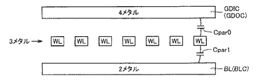
ローカルデータ線対LDUおよびLDLは、それぞれ、分離ゲートIGUおよびIGLを介してセンスアンプSAおよびライトドライバWDRに結合される。分離ゲートIGUおよびIGLは、図1に示すサブアレイ分離/接続部ISK(ISK0−ISKn)に含まれる。分離ゲートIGUおよびIGLは、選択サブアレイのローカルデータ線対をセンスアンプSAおよびライトドライバWDRに結合する。ライトドライバWDRは、このメモリブロックMBの選択時、グローバル書込データ線GDIC上の内部書込データに従ってメモリセルへの書込データを生成する。センスアンプSAの出力信号は、リードドライバRDRを介してグローバル読出データ線GDOCに伝達される。これらのグローバル書込データ線GDICおよびグローバル読出データ線GDOCが、図1に示すグローバルデータバスGDB(GDB0−GDBn)に対応する。図2においては、グローバルデータバスが、書込データ線と読出データ線とが別々に設けられるIO分離構造の場合を一例として示す。このグローバルデータバスGDOCは、共通IO構造のバスであっても良い。 Local data line pair LDU and LDL are coupled to sense amplifier SA and write driver WDR via isolation gates IGU and IGL, respectively. Isolation gates IGU and IGL are included in subarray isolation / connection unit ISK (ISK0-ISKn) shown in FIG. Isolation gates IGU and IGL couple the local data line pair of the selected subarray to sense amplifier SA and write driver WDR. Write driver WDR generates write data to the memory cell in accordance with internal write data on global write data line GDIC when memory block MB is selected. The output signal of sense amplifier SA is transmitted to global read data line GDOC via read driver RDR. These global write data line GDIC and global read data line GDOC correspond to global data buses GDB (GDB0 to GDBn) shown in FIG. FIG. 2 shows an example in which the global data bus has an IO isolation structure in which a write data line and a read data line are provided separately. The global data bus GDOC may be a common IO structure bus.
この図2に示すように、分離ゲートIGUおよびIGLを用いて、選択サブアレイのローカルデータ線対をセンスアンプSAに結合する。非選択のサブアレイをセンスアンプから分離する。したがって、これらのローカルデータ線LDUおよびLDLの寄生容量CpuおよびCplは、一方のみがセンスアンプSAに結合され、このセンスアンプSAのセンスノードの負荷が軽減され、高速で、このセンスアンプSAのセンスノード電位を変化させることができる。 As shown in FIG. 2, the local data line pair of the selected subarray is coupled to sense amplifier SA using isolation gates IGU and IGL. The non-selected subarray is separated from the sense amplifier. Therefore, only one of parasitic capacitances Cpu and Cpl of local data lines LDU and LDL is coupled to sense amplifier SA, the load on the sense node of sense amplifier SA is reduced, and the sense amplifier SA senses at high speed. The node potential can be changed.
特に、ライトドライバWDRに対しても、分離ゲートIGUおよびIGLを接続することにより、このセンスアンプSAに対するライトドライバWDRの負荷を分離することができ、センスアンプSAの負荷をさらに軽減することができる。特に、SRAMにおいては、この接続/分離部においては、センスアンプ、リードアンプおよびライトドライバが配置され、そのサブアレイ間のセンスアンプ配置領域の占有面積は大きい。従って、ローカルデータ線を、サブアレイMAUおよびMALに共通に配置した場合、その配線長が長くなり、負荷が大きくなる。このため、ビット線を分割構造としてセンスアンプに接続することによりビット線負荷を低減する効果が、ローカルデータ線の負荷により損なわれる。ローカルデータ線を、分割構造としてサブアレイそれぞれに設け、選択サブアレイのみをセンスアンプに接続する。この分割ローカルデータ線構造により、センスアンプSAに対するローカルデータ線の負荷を軽減することができ、ビット線分割構造の効果を十全に発揮することができる。 In particular, even for write driver WDR, by connecting the isolation gates IGU and IGL, can separate the load of write driver WDR for the sense amplifier SA, it is possible to further reduce the load of the sense amplifier SA . In particular, in the SRAM, a sense amplifier, a read amplifier, and a write driver are arranged in this connection / separation unit, and the area occupied by the sense amplifier arrangement region between the subarrays is large. Therefore, when the local data lines are arranged in common in the sub-arrays MAU and MAL, the wiring length is increased and the load is increased. For this reason, the effect of reducing the bit line load by connecting the bit line to the sense amplifier as a divided structure is impaired by the load of the local data line. A local data line is provided in each subarray as a divided structure, and only the selected subarray is connected to the sense amplifier. With this divided local data line structure, the load of the local data line on the sense amplifier SA can be reduced, and the effect of the bit line divided structure can be fully exhibited.
また、メモリセル行の数が増大しても、メモリブロックの数を増大させることにより、各メモリブロックのビット線負荷の増大を抑制することができ、高速のデータ読出を実現することができる。グローバル読出データ線の長さが長くなるもののリードドライバが結合されるだけであり、その負荷の増大は小さく、また、リードドライバにより高速でグローバル読出データ線GDOCを駆動することができる。以下、各部の構成について具体的に説明する。 Even if the number of memory cell rows increases, by increasing the number of memory blocks, an increase in the bit line load of each memory block can be suppressed, and high-speed data reading can be realized. Although the length of the global read data line is increased, only the read driver is coupled, the increase in the load is small, and the global read data line GDOC can be driven at high speed by the read driver. Hereinafter, the structure of each part is demonstrated concretely.
図3は、この発明に従う半導体記憶装置において用いられるメモリセルMCの構成の一例を示す図である。図3において、メモリセルMCは、電源ノードと記憶ノードSNの間に接続されかつそのゲートが記憶ノードSNCに接続されるPチャネルMOSトランジスタP1と、電源ノードと記憶ノードSNCの間に接続されかつそのゲートが記憶ノードSNに接続されるPチャネルMOSトランジスタP2と、記憶ノードSNと接地ノードの間に接続されかつそのゲートが記憶ノードSNCに接続されるNチャネルMOSトランジスタN1と、記憶ノードSNCと接地ノードとの間に接続されかつそのゲートが記憶ノードSNに接続されるNチャネルMOSトランジスタN2と、ワード線WL上の信号電位に応答して、記憶ノードSNおよびSNCをそれぞれビット線BLおよびBLCに接続するNチャネルMOSトランジスタN3およびN4を含む。 FIG. 3 shows an example of the configuration of memory cell MC used in the semiconductor memory device according to the present invention. In FIG. 3, a memory cell MC is connected between a power supply node and a storage node SN and connected between the power supply node and the storage node SNC, a P channel MOS transistor P1 whose gate is connected to the storage node SNC, and P channel MOS transistor P2 having its gate connected to storage node SN, N channel MOS transistor N1 having its gate connected to storage node SNC and connected between storage node SN and ground node, storage node SNC, In response to the signal potential on word line WL, N channel MOS transistor N2 connected to ground node and having its gate connected to storage node SN, and storage nodes SN and SNC are connected to bit lines BL and BLC, respectively. Including N channel MOS transistors N3 and N4 connected to .
これらのMOSトランジスタP1、P2、N1およびN2が、いわゆるインバータラッチ回路を構成し、記憶ノードSNおよびSNCに、相補データをラッチする。このメモリセルMCは、フルCMOS構成のスタティック型メモリセルであり、電源ノードに電源電圧が供給されている間、記憶ノードSNおよびSNCに、相補データを保持する。 These MOS transistors P1, P2, N1 and N2 form a so-called inverter latch circuit, and latch complementary data in storage nodes SN and SNC. This memory cell MC is a static memory cell having a full CMOS configuration, and holds complementary data in storage nodes SN and SNC while a power supply voltage is supplied to the power supply node.
データ読出時においては、ワード線WL選択状態へ駆動され、応じてMOSトランジスタN3およびN4が導通し、ビット線BLおよびBLCに、記憶ノードSNおよびSNCの記憶データに応じた電位変化が相補的に生じる。このビット線BLおよびBLCの電位変化を、図2に示すセンスアンプSAへ転送して、増幅する。 At the time of data reading, MOS transistor N3 and N4 are driven in response to the word line WL selected state, and potential changes corresponding to storage data of storage nodes SN and SNC are complementarily applied to bit lines BL and BLC. Arise. The potential changes of the bit lines BL and BLC are transferred to the sense amplifier SA shown in FIG. 2 and amplified.
図4は、この発明の実施の形態1に従う半導体記憶装置の1つのIOブロックIOBの構成の一例を概略的に示す図である。図4において、IOブロックIOBは、一例として、4つのメモリブロックMB[0]−MB[3]を含む。これらのメモリブロックMB[0]−MB[3]は、各々、同一構成を有するため、図4においては、メモリブロックMB[3]の構成を代表的に示し、残りのメモリブロックMB[0]−MB[2]については、単にブロックのみで示す。これらのメモリブロックMB[0]−MB[3]は、共通にグローバルデータ線GDOCおよびGDICに結合される。 FIG. 4 schematically shows an example of a configuration of one IO block IOB of the semiconductor memory device according to the first embodiment of the present invention. In FIG. 4, the IO block IOB includes four memory blocks MB [0] -MB [3] as an example. Since these memory blocks MB [0] -MB [3] have the same configuration, FIG. 4 representatively shows the configuration of the memory block MB [3], and the remaining memory blocks MB [0]. -For MB [2], only block is indicated. These memory blocks MB [0] -MB [3] are commonly coupled to global data lines GDOC and GDIC.
メモリブロックMB[3]は、2つのサブアレイMAUおよびMALを含む。これらのサブアレイMAUおよびMAL各々においては、メモリセルMCが行列状に配列され、メモリセルMCの各列に対応してビット線対が配設され、また、メモリセルの各行に対応してワード線WLが配置される。図4においては、サブアレイMAUおよびMAL各々において、2行4列に配列されるメモリセルMCを一例として示す。メモリセルMCの各行に対応してワード線WL[0]およびWL[1]が配設される。ビット線対は、メモリセルMCの各列に対応して配置されるビット線BL[0],BLC[0]−BL[3],BLC[3]を含む。サブアレイMALにおいても同様に、2行4列に配列されたメモリセルMCに対して、ワード線およびビット線対が、それぞれメモリセル行およびメモリセル列に対応して配設される。この図4においては、図面の煩雑化を避けるため、メモリサブアレイMALにおいては、ビット線対BLP、ビット線BLおよびBLCおよびワード線WLの符号を代表的に示す。 Memory block MB [3] includes two subarrays MAU and MAL. In these subarrays MAU and MAL each memory cell MC are arranged in rows and columns, the bit line pair corresponding to each column of memory cells MC are arranged, also, the word line corresponding to each row of memory cells WL is arranged. In FIG. 4, memory cells MC arranged in 2 rows and 4 columns are shown as an example in each of subarrays MAU and MAL. Corresponding to each row of memory cells MC, word lines WL [0] and WL [1] are arranged. The bit line pair includes bit lines BL [0], BLC [0] -BL [3], BLC [3] arranged corresponding to each column of memory cells MC. Similarly, in subarray MAL, word line and bit line pairs are arranged corresponding to memory cell rows and memory cell columns, respectively, for memory cells MC arranged in 2 rows and 4 columns. In FIG. 4, in order to avoid complication of the drawing, in the memory sub-array MAL, symbols of the bit line pair BLP, the bit lines BL and BLC, and the word line WL are representatively shown.
サブアレイMAUおよびMALそれぞれに対して、ワード線WLを、与えられたアドレス信号に従って選択状態へ駆動するためのロウデコード回路XDが設けられる。サブアレイMAUおよびMALの間に、選択サブアレイのメモリセルデータの読出および選択メモリセルへのデータの書込を行なうカラム回路YCが設けられる。これらのメモリブロックMB[0]−MB[3]のカラム回路YCは、グローバルデータ線GDOCおよびGDICに共通に結合され、入出力回路IOKとの間で内部データの転送を行なう。入出力回路IOKは、図1に示す入出力回路IOCKのうちの1ビットのデータを入出力する回路部分を示す。 For each of subarrays MAU and MAL, row decode circuit XD is provided for driving word line WL to a selected state in accordance with a given address signal. Between subarrays MAU and MAL, column circuit YC for reading memory cell data of the selected subarray and writing data into the selected memory cell is provided. The column circuits YC of these memory blocks MB [0] -MB [3] are commonly coupled to the global data lines GDOC and GDIC, and transfer internal data to / from the input / output circuit IOK. The input / output circuit IOK indicates a circuit portion for inputting / outputting 1-bit data in the input / output circuit IOCK shown in FIG.
カラム回路YCは、図1に示されるサブアレイ分離/接続部ISKおよび書込/読出回路WRKに含まれ、メモリブロックMBに対応してサブアレイMAUおよびMALの間に配置される。すなわち、図1に示すサブアレイ分離/接続部ISKおよび書込/読出回路WRKが、各メモリブロックに対応してカラム回路YCとして分割かつ分散して配置される。従って、カラム回路YCは、その構成は後に詳細に説明するが、サブアレイの分離/接続および書込/読出の機能を実現する。 Column circuit YC is included in subarray isolation / connection portion ISK and write / read circuit WRK shown in FIG. 1, it is arranged between the subarrays MAU and MAL corresponding to the memory block MB. That is, the subarray isolation / connection unit ISK and the write / read circuit WRK shown in FIG. 1 are divided and distributed as column circuits YC corresponding to each memory block. Therefore, the column circuit YC, which will be described in detail later, realizes subarray separation / connection and write / read functions.
メモリブロックMB[0]−MB[3]の動作を制御するために、外部からのクロック信号CLK、この半導体記憶装置が選択されたことを示すチップセレクト信号CSC、およびデータ書込を示す書込信号WECに従って、内部クロック信号ICLK、リードイネーブル信号REおよび内部書込指示信号(図示せず)を生成する制御回路CTLが設けられる。この制御回路CTLからの内部クロック信号ICLKおよびリードイネーブル信号REが、アドレス信号ADとともに、メモリブロックMB[0]−MB[3]それぞれに設けられるローカル制御回路LCへ与えられる。このローカル制御回路LCに対しては、また、内部書込指示信号が与えられブロック単位での書込の制御が行われるが、図4においては、この書込指示信号(ライトイネーブル信号)の経路は示していない。 To control the operation of the memory blocks MB [0] -MB [3], the writing indicating the clock signal CLK from the outside, a chip select signal CSC indicating that the semiconductor memory device is selected, and the data write A control circuit CTL is provided for generating internal clock signal ICLK, read enable signal RE, and internal write instruction signal (not shown) in accordance with signal WEC. Internal clock signal ICLK and read enable signal RE from control circuit CTL are applied to local control circuit LC provided in each of memory blocks MB [0] -MB [3] together with address signal AD. This local control circuit LC is also supplied with an internal write instruction signal to control writing in block units. In FIG. 4, the path of this write instruction signal (write enable signal) is controlled. Is not shown.
ローカル制御回路LCは、このアドレス信号ADに含まれるメモリブロック選択信号およびサブアレイ選択信号に従って、データ読出時、内部クロック信号ICLKおよびリードイネーブル信号REの規定するタイミングでカラム回路YCを選択的に活性化する。 Local control circuit LC, according to the memory block select signals and subarray select signal included in the address signal AD, data reading, selectively activate column circuit YC at the timing that defines the internal clock signal ICLK and a read enable signal RE To do.
メモリブロックMB[0]−MB[3]各々において、サブアレイMAUおよびMALを設け、それらの間にカラム回路YCを配置することにより、ビット線BLおよびBLCが、各サブアレイMAUおよびMAL内においてのみ延在し、ビット線分割構造を実現して、ビット線の長さを短くし、ビット線に接続されるメモリセルの数を低減して、ビット線負荷を軽減する。 In each of memory blocks MB [0] -MB [3], subarrays MAU and MAL are provided, and column circuit YC is arranged therebetween, so that bit lines BL and BLC extend only in each subarray MAU and MAL. Therefore, the bit line division structure is realized, the length of the bit line is shortened, the number of memory cells connected to the bit line is reduced, and the bit line load is reduced.
さらに、カラム回路YCにおいて、ローカル制御回路LCの制御の下に、選択サブアレイのみをセンスアンプおよびライトドライバに接続することにより、さらに、このカラム回路の駆動負荷を軽減する。 Further, in the column circuit YC, the drive load of the column circuit is further reduced by connecting only the selected sub-array to the sense amplifier and the write driver under the control of the local control circuit LC.
入出力回路IOKは、データ読出時、制御回路CTLからのリードイネーブル信号REの活性化に応答して、グローバル読出データ線GDOC上の信号に従って外部読出データDOを生成する。 Input / output circuit IOK generates external read data DO according to a signal on global read data line GDOC in response to activation of read enable signal RE from control circuit CTL during data reading.
図5は、図4に示すカラム回路YCの構成を概略的に示す図である。このカラム回路YCは、サブアレイMAUのビット線対BLU[0],BLCU[0]−BLU[3],BLCU[3]それぞれに対して設けられるビット線プリチャージ回路BPCGと、サブアレイMALのビット線対BLL[0],BLCL[0]−BLL[3],BLCL[3]それぞれに対して設けられるビット線プリチャージ回路BPCGと、列選択信号YSU[0]−YSU[3]に従ってサブアレイMAUのビット線対を選択してローカルデータ線DUおよびDCUに結合する列選択回路YTGUと、列選択信号YSL[0]−YSL[3]に従ってサブアレイMALの指定された列のビット線対を選択して、ローカルデータ線DLおよびDCLにそれぞれ結合する列選択回路YTGLを含む。図2に示すローカルデータ線対LDUが、ローカルデータ線DUおよびDCUに対応し、図2に示すローカルデータ線対LDLが、ローカルデータ線DLおよびDCLに対応する。 FIG. 5 schematically shows a structure of column circuit YC shown in FIG. This column circuit YC includes a bit line precharge circuit BPCG provided for each of bit line pairs BLU [0], BLCU [0] -BLU [3], BLCU [3] of the subarray MAU, and bitlines of the subarray MAL. The bit line precharge circuit BPCG provided for each of the pairs BLL [0], BLCL [0] -BLL [3], BLCL [3] and the subarray MAU according to the column selection signals YSU [0] -YSU [3] A column selection circuit YTGU that selects a bit line pair and couples to local data lines DU and DCU, and selects a bit line pair of a specified column of subarray MAL according to column selection signals YSL [0] -YSL [3] Column select circuits YTGL coupled to local data lines DL and DCL, respectively. The local data line pair LDU shown in FIG. 2 corresponds to the local data lines DU and DCU, and the local data line pair LDL shown in FIG. 2 corresponds to the local data lines DL and DCL.
ビット線プリチャージ回路BPCGは、プリチャージ指示信号PECの活性化時、対応のビット線を、所定のたとえば電源電位レベルにプリチャージする。 Bit line precharge circuit BPCG precharges the corresponding bit line to a predetermined power supply potential level, for example, when precharge instruction signal PEC is activated.
列選択回路YTGUおよびYTGLは、それぞれ対応の列選択信号YSU[0]−YSU[3]およびYSL[0]−YSL[3]の1つが選択状態に駆動されると、対応のビット線対をローカルデータ線DU,DCUおよびDL,DCLに結合する。ローカルデータ線として、サブアレイMAUに対するローカルデータ線DUおよびDCUとサブアレイMALに対するローカルデータ線DLおよびDCLを別々に設けることにより、これらのローカルデータ線の負荷を軽減する。 Column selection circuits YTGU and YTGL respectively drive corresponding bit line pairs when one of corresponding column selection signals YSU [0] -YSU [3] and YSL [0] -YSL [3] is driven to a selected state. Coupled to local data lines DU, DCU and DL, DCL. By separately providing local data lines DU and DCU for the subarray MAU and local data lines DL and DCL for the subarray MAL as local data lines, the load on these local data lines is reduced.
ローカルデータ線DUおよびDCUの間に、データ線プリチャージ回路DPCGが設けられ、またローカルデータ線DLおよびDCLの間にも、これらのローカルデータ線をプリチャージするデータ線プリチャージ回路DPCGが設けられる。これらのデータ線プリチャージ回路DPCGは、ビット線プリチャージ回路BPCGと同様、プリチャージ指示信号PECの活性化に応答して、対応のローカルデータ線の所定電位レベルへのプリチャージを実行する。 A data line precharge circuit DPCG is provided between the local data lines DU and DCU, and a data line precharge circuit DPCG for precharging these local data lines is also provided between the local data lines DL and DCL. . Similar to bit line precharge circuit BPCG, these data line precharge circuits DPCG execute precharge of the corresponding local data lines to a predetermined potential level in response to activation of precharge instruction signal PEC.
カラム回路YCは、さらに、分離接続制御回路として、センス活性化信号SEを反転するインバータG100と、インバータG100の出力信号SECとサブアレイ指定信号BSCUとを受けるNANDゲートG101と、インバータG100の出力信号SECとサブアレイ指定信号BSCLとを受けるNANDゲートG102と、NANDゲートG102の出力信号がLレベルのとき導通し、ローカルデータ線DUおよびDCUを、センスノードSIおよびSICにそれぞれ結合するPチャネルMOSトランジスタP100およびP101と、NANDゲートG101の出力信号がLレベルのとき導通し、ローカルデータ線DLおよびDCLをセンスノードSIおよびSICへ結合するPチャネルMOSトランジスタP102およびP103を含む。 The column circuit YC further serves as a separate connection control circuit, an inverter G100 that inverts the sense activation signal SE, a NAND gate G101 that receives the output signal SEC of the inverter G100 and the subarray designation signal BSCU, and an output signal SEC of the inverter G100. NAND gate G102 receiving subarray designating signal BSCL, and P channel MOS transistor P100 which conducts when the output signal of NAND gate G102 is at L level and couples local data lines DU and DCU to sense nodes SI and SIC, respectively. P-channel MOS transistors P102 and P10 that conduct when P101 and the output signal of NAND gate G101 are at L level and couple local data lines DL and DCL to sense nodes SI and SIC Including the.
サブアレイ指定信号BSCLおよびBSCUは、サブアレイ選択信号を構成し、それぞれ、活性化時、サブアレイMALおよびMAUを指定する。 Subarray designation signals BSCL and BSCU constitute a subarray selection signal, and designate subarrays MAL and MAU, respectively, when activated.
センスノードSIおよびSICに結合されるセンスアンプSAは、一例として、ラッチ型センスアンプで構成され、センス活性化信号SEの活性化時、これらのセンスノードSIおよびSICの電位を差動的に増幅して相補信号SOおよびSOCを生成する。しかしながら、このセンスアンプSAは、カレントミラー型センスアンプで構成されても良い。 Sense amplifier SA coupled to sense nodes SI and SIC is, for example, a latch type sense amplifier, and differentially amplifies the potentials of sense nodes SI and SIC when sense activation signal SE is activated. Thus, complementary signals SO and SOC are generated. However, the sense amplifier SA may be formed of a current mirror type sense amplifier.
ローカルデータ線DUおよびDCUおよびローカルデータ線DLおよびDCLには、それぞれ、データ線プリチャージ回路DPCGが設けられ、それぞれ、プリチャージ指示信号PECの活性化時、対応のデータ線プリチャージ回路DPCGにより所定電位レベルにプリチャージされる。これらのローカルデータ線対に対してデータ線プリチャージ回路を配置することにより。ローカルデータ線の負荷をサブアレイMAUおよびMAL両者に対して同一とすることができ、選択サブアレイに係らず同一タイミングでセンス動作を開始することができ、センスマージンを大きくすることができる。 Each of local data lines DU and DCU and local data lines DL and DCL is provided with a data line precharge circuit DPCG. Each of data lines precharge circuit DPCG is predetermined by corresponding data line precharge circuit DPCG when precharge instruction signal PEC is activated. Precharged to potential level. By arranging a data line precharge circuit for these local data line pairs. The load on the local data line can be made the same for both the subarrays MAU and MAL, the sensing operation can be started at the same timing regardless of the selected subarray, and the sense margin can be increased.
ローカルデータ線とセンスアンプSAの接続を制御するために、PチャネルMOSトランジスタP100−P103を利用することにより、ローカルデータ線DU,DCUおよびDL,DCLが、たとえば電源電圧レベルにプリチャージされる状態であっても、MOSトランジスタのしきい値電圧損失を伴うことなく、データ線電位を、センスノードSIおよびSICへ伝達することができる。 A state in which local data lines DU, DCU and DL, DCL are precharged to, for example, a power supply voltage level by using P channel MOS transistors P100-P103 to control connection between the local data line and sense amplifier SA. Even so, the data line potential can be transmitted to the sense nodes SI and SIC without the threshold voltage loss of the MOS transistor.
リードドライバRDRは、インバータG100の出力信号の活性化時(Lレベルのとき)イネーブルされ、センスアンプSAの相補出力信号SOおよびSOCに従ってグローバル読出データ線GDOCを駆動する。 Read driver RDR is enabled when the output signal of inverter G100 is activated (at the L level), and drives global read data line GDOC in accordance with complementary output signals SO and SOC of sense amplifier SA.
このリードドライバRDRは、センスノードSIの信号SOとインバータG100の出力する補のセンス活性化信号SECとを受けるNORゲートG110と、センスノードSICの信号SOCと補のセンス活性化信号SECとを受けるNORゲートG112と、NORゲートG110の出力信号を反転するインバータG111と、インバータG111の出力信号がLレベルのときに、グローバル読出データ線GDOCを電源ノードに結合するPチャネルMOSトランジスタP110と、NORゲートG112の出力信号がHレベルのとき導通し、グローバル読出データ線GDOCを接地ノードに結合するNチャネルMOSトランジスタN110を含む。 Read driver RDR receives NOR gate G110 receiving signal SO of sense node SI and complementary sense activation signal SEC output from inverter G100, and receives signal SOC of sense node SIC and complementary sense activation signal SEC. NOR gate G112, inverter G111 for inverting the output signal of NOR gate G110, P-channel MOS transistor P110 for coupling global read data line GDOC to the power supply node when the output signal of inverter G111 is at L level, and NOR gate N channel MOS transistor N110 which conducts when the output signal of G112 is at H level and couples global read data line GDOC to the ground node is included.
補のセンス活性化信号SECがHレベルであり、センスアンプSAが非活性状態のときには、NORゲートG110およびG112の出力信号はともにLレベルであり、MOSトランジスタP110およびN110がオフ状態となり、このリードドライバRDRは出力ハイインピーダンス状態にある。補のセンス活性化信号SECがLレベルとなると、NORゲートG110およびG112がインバータとして動作し、センスアンプSAの出力信号SOおよびSOCに従って、MOSトランジスタP110およびN110の一方がオン状態となり、グローバル読出データ線GDOCが、電源電位または接地電圧に駆動される。 When complementary sense activation signal SEC is at the H level and sense amplifier SA is in the inactive state, the output signals of NOR gates G110 and G112 are both at the L level, and MOS transistors P110 and N110 are in the off state. Driver RDR is in an output high impedance state. When complementary sense activation signal SEC attains L level, NOR gates G110 and G112 operate as inverters, and one of MOS transistors P110 and N110 is turned on in accordance with output signals SO and SOC of sense amplifier SA. The line GDOC is driven to the power supply potential or the ground voltage.
ライトドライバWDRは、グローバル書込データ線GDIC上の信号を受けるインバータIV1と、インバータIV1の出力信号を反転するインバータIV2と、相補書込活性化信号WENCおよびWENの活性化に応答して、インバータIV1の出力信号を反転するトライステートインバータTIV1と、相補書込活性化信号WENおよびWENCの活性化に応答して活性化され、インバータIV2の出力信号を反転するトライステートインバータTIV2を含む。これらのトライステートインバータTIV1およびTIV2は、非活性化時出力ハイインピーダンス状態にある。1つのメモリブロックにおいて、1つのインバータIV1のみを、グローバル書込データ線GDICに接続することにより、このグローバル書込データ線GDICの負荷を軽減する。 Write driver WDR responds to activation of inverter IV1 receiving a signal on global write data line GDIC, inverter IV2 inverting the output signal of inverter IV1, and complementary write activation signals WENC and WEN. It includes a tristate inverter TIV1 that inverts the output signal of IV1, and a tristate inverter TIV2 that is activated in response to activation of complementary write activation signals WEN and WENC and inverts the output signal of inverter IV2. These tri-state inverters TIV1 and TIV2 are in an output high impedance state when inactive. By connecting only one inverter IV1 to the global write data line GDIC in one memory block, the load on the global write data line GDIC is reduced.
図2に示す分離ゲートIGUおよびIGLの書込データ転送部は、サブアレイ指定信号BSCUと書込活性化信号WENCを受けるNORゲートG103と、NORゲートG103の出力信号がHレベルのとき導通し、トライステートインバータTIV1およびTIV2の出力信号をそれぞれローカルデータ線DCUおよびDUに伝達するNチャネルMOSトランジスタN101およびN100と、補の書込活性化信号WENCとサブアレイ指定信号BSCLとを受けるNORゲートG104と、NORゲートG104の出力信号がHレベルのときに、トライステートインバータTIV1およびTIV2の出力信号を、それぞれ、ローカルデータ線DCLおよびDLに伝達するNチャネルMOSトランジスタN103およびN102を含む。 The write data transfer units of isolation gates IGU and IGL shown in FIG. 2 are turned on when NOR gate G103 receiving subarray designating signal BSCU and write activation signal WENC and the output signal of NOR gate G103 are at the H level. N channel MOS transistors N101 and N100 transmitting the output signals of state inverters TIV1 and TIV2 to local data lines DCU and DU, NOR gate G104 receiving complementary write activation signal WENC and subarray designating signal BSCL, NOR N channel MOS transistors N103 and N102 transmitting the output signals of tristate inverters TIV1 and TIV2 to local data lines DCL and DL, respectively, when the output signal of gate G104 is at the H level are included.
サブアレイ指定信号BSCUおよびBSCLは、活性化時(Lレベルのとき)、それぞれ、サブアレイMAUおよびMALを指定する。したがって、データ書込時、補の書込活性化信号WENCが活性化されてLレベルとなると、NORゲートG103およびG104のうち、選択サブアレイに対して設けられたNORゲートの出力信号がHレベルとなり、対応のNチャネルMOSトランジスタN101,N100またはN103,N102が導通し、トライステートバッファTIV1およびTIV2の出力信号が、選択サブアレイに対するローカルデータ線DCU,DUまたはDCL,DLに伝達される。 Subarray designation signals BSCU and BSCL designate subarrays MAU and MAL, respectively, when activated (when at L level). Therefore, at the time of data writing, when complementary write activation signal WENC is activated and becomes L level, among NOR gates G103 and G104, the output signal of the NOR gate provided for the selected subarray becomes H level. Corresponding N channel MOS transistors N101, N100 or N103, N102 are rendered conductive, and the output signals of tristate buffers TIV1 and TIV2 are transmitted to local data lines DCU, DU or DCL, DL for the selected subarray.
対応のサブアレイが非選択状態のときには、サブアレイ指定信号BSCUまたはBSCLは、Hレベルであり、NORゲートG103およびG104のうち非選択サブアレイに対するNORゲートの出力信号がLレベルとなり、非選択サブアレイに対するローカルデータ線の書込データの伝達は禁止される。 When the corresponding sub-array is in the non-selected state, sub-array designating signal BSCU or BSCL is at the H level, the NOR gate output signal for the non-selected sub-array among NOR gates G103 and G104 is at the L level, and the local data for the non-selected sub-array Transmission of line write data is prohibited.
ローカルデータ線DU,DCUおよびDL,DCLを各サブアレイに対応して分割構造とし、分離ゲートP100−P103およびN100−N103を用いて、選択サブアレイに対するローカルデータ線のみをセンスアンプSAまたはライトドライバWDRに接続することにより、ローカルデータ線DU,DCUおよびDL,DCLの負荷が軽減される。したがって、データ読出時、このラッチ型センスアンプSAに対し、高速で、選択メモリセルデータを伝達して、センス動作を行なってデータの読出を行なうことができる。 The local data lines DU, DCU and DL, DCL are divided to correspond to each subarray, and only the local data lines for the selected subarray are supplied to the sense amplifier SA or the write driver WDR by using the separation gates P100-P103 and N100-N103. By connecting, the load on the local data lines DU, DCU and DL, DCL is reduced. Therefore, at the time of data reading, the selected memory cell data can be transmitted to latch type sense amplifier SA at a high speed, and the data can be read by performing a sensing operation.
なお、図5に示す構成においては、スタンバイ時において、トライステートバッファTIV1およびTIV2が出力ハイインピーダンスとなり、また,MOSトランジスタN100−N103が、全てオフ状態となる。この場合、トライステートインバータTIV1およびTIV2の出力にスタンバイ時に電源電圧などの所定電圧レベルにプリチャージするプリチャージ回路が設けられても良く、また、MOSトランジスタN100−N103が、スタンバイ時に導通状態となる構成が利用されてもよい。 In the configuration shown in FIG. 5, at the time of standby, tristate buffers TIV1 and TIV2 are set to output high impedance, and all MOS transistors N100-N103 are turned off. In this case, a precharge circuit for precharging the output of the tristate inverters TIV1 and TIV2 to a predetermined voltage level such as a power supply voltage at the time of standby may be provided, and the MOS transistors N100 to N103 are rendered conductive at the time of standby. A configuration may be utilized.
図6は、図5に示すセンスアンプSAの構成の一例を示す図である。図6において、センスアンプSAは、電源ノードとセンスノードSIの間に接続されかつそのゲートがセンスノードSICに接続されるPチャネルMOSトランジスタPQ1と、電源ノードとセンスノードSICの間に接続されかつそのゲートがセンスノードSIに接続されるPチャネルMOSトランジスタPQ2と、センスノードSIと共通ソースノードCSNDの間に接続されかつそのゲートがセンスノードSICに接続されるNチャネルMOSトランジスタNQ1と、センスノードSICと共通ソースノードCSNDの間に接続されかつそのゲートがセンスノードSIに接続されるNチャネルMOSトランジスタNQ2と、センス活性化信号SEの活性化時共通ソースノードCSNDを接地電位を供給する接地ノードに結合するNチャネルMOSトランジスタNQ3を含む。 FIG. 6 is a diagram showing an example of the configuration of sense amplifier SA shown in FIG. 6, the sense amplifier SA includes P-channel MOS transistors PQ1 connected and having a gate between the power supply node and the sense node SI is connected to the sense node SIC, is connected between the power supply node and the sense node SIC and P-channel MOS transistor PQ2 having its gate connected to sense node SI, N-channel MOS transistor NQ1 having its gate connected to sense node SIC and connected between sense node SI and common source node CSND, and sense node It is connected between the SIC and the common source node CSND and the N-channel MOS transistor NQ2 having its gate connected to sense node SI, a ground node supplying the ground potential to the common source node CSND activation of sense activation signal SE N tea to join Including Le MOS transistor NQ3.
この図6に示すセンスアンプSAは、MOSトランジスタPQ1,PQ2,NQ1およびNQ2により活性化時インバータラッチを構成する交差結合型センスアンプ、すなわちラッチ型センスアンプである。センス活性化信号SEがLレベルの非活性状態のときには、センスノードSIおよびSICは、プリチャージ電圧レベルにあるかまたは読出データ信号のレベルにある。共通ソースノードCSNDは、この状態においてはハイレベル(プリチャージ電圧に近いレベル)にある。 The sense amplifier SA shown in FIG. 6 is a cross-coupled sense amplifier that constitutes an inverter latch when activated by MOS transistors PQ1, PQ2, NQ1, and NQ2, that is, a latch-type sense amplifier. When sense activation signal SE is in the inactive state of L level, sense nodes SI and SIC are at the precharge voltage level or at the level of the read data signal. In this state, the common source node CSND is at a high level (a level close to the precharge voltage).
センス活性化信号SEがHレベルとなると、MOSトランジスタNQ3がオン状態となり、共通ソースノードCSNDが接地電位レベルに設定される。センスノードSIおよびSICは、プリチャージ電圧レベルに近い電圧レベルであり、これらのセンスノードSIおよびSICの低いほうのセンスノードが、MOSトランジスタNQ1またはNQ2により接地電位レベルに放電され、一方、これらのセンスノードSIおよびSICのうちの電位の高いほうのセンスノードは、MOSトランジスタPQ1またはPQ2により電源電圧レベル(電源ノードの電圧レベル)に駆動され、これらのセンスノードSIおよびSICの信号電位差が差動的に増幅され、相補信号SOおよびSOCが生成される。 When sense activation signal SE becomes H level, MOS transistor NQ3 is turned on, and common source node CSND is set to the ground potential level. Sense nodes SI and SIC are at a voltage level close to the precharge voltage level, and the lower sense node of these sense nodes SI and SIC is discharged to the ground potential level by MOS transistor NQ1 or NQ2, while these The sense node with the higher potential of sense nodes SI and SIC is driven to the power supply voltage level (voltage level of the power supply node) by MOS transistor PQ1 or PQ2, and the signal potential difference between these sense nodes SI and SIC is differential. Are amplified to produce complementary signals SO and SOC.
この交差結合型センスアンプにおいて、センスノードSIおよびSICを、接地電位レベルへ駆動するセンス活性化トランジスタのみが設けられているのは、センスノードSIおよびSICは、電源電圧レベルのプリチャージ電圧レベルに設定されるためである。 In this cross-coupled sense amplifier, only sense activation transistors for driving sense nodes SI and SIC to the ground potential level are provided because sense nodes SI and SIC are at the precharge voltage level of the power supply voltage level. This is because it is set.
この図6に示すような交差結合型センスアンプSAを利用することにより、微小電位差を高速で増幅して、CMOSレベルの信号(電源電圧と接地電位との間で変化する信号)を生成して、相補信号SOおよびSOCを生成することができる。 By utilizing the cross-coupled sense amplifier SA as shown in FIG. 6, a minute potential difference is amplified at a high speed to generate a CMOS level signal (a signal changing between the power supply voltage and the ground potential). Complementary signals SO and SOC can be generated.
図7は、図5に示すビット線、ローカルデータ線をそれぞれプリチャージするプリチャージ回路BPCGおよびDPCGの構成の一例を示す図である。これらのビット線およびローカルデータ線をプリチャージするプリチャージ回路BPCGおよびDPCGの構成は同じであり、図7においては、プリチャージ回路PCGをこれらのプリチャージ回路の代表的として示す。プリチャージ回路PCGは、プリチャージ活性化信号PECの活性化に応答して、電源電位をノードND0およびND1にそれぞれ伝達するPチャネルMOSトランジスタPQ3およびPQ4を含む。ノードND0およびND1が、それぞれ、相補ビット線または相補ローカルデータ線に接続される。 FIG. 7 is a diagram showing an example of the configuration of precharge circuits BPCG and DPCG for precharging the bit lines and local data lines shown in FIG. 5, respectively. The configurations of precharge circuits BPCG and DPCG for precharging these bit lines and local data lines are the same. In FIG. 7, precharge circuit PCG is shown as a representative of these precharge circuits. Precharge circuit PCG includes P channel MOS transistors PQ3 and PQ4 transmitting power supply potentials to nodes ND0 and ND1, respectively, in response to activation of precharge activation signal PEC. Nodes ND0 and ND1 are connected to complementary bit lines or complementary local data lines, respectively.
プリチャージ活性化信号PECは、活性化時Lレベルであり、ノードND0およびND1は、電源ノードの電圧(電源電圧)レベルにプリチャージされる。プリチャージ活性化信号PECが不活性状態となると、これらのMOSトランジスタPQ3およびPQ4が、非導通状態となり、ノードND0およびND1が電源ノードから分離される。このプリチャージ活性化信号PECは、メモリブロック単位で活性/非活性が制御され、選択メモリブロックにおいてプリチャージ動作が停止されてデータの書込または読出が行われる。非選択メモリブロックは、プリチャージ状態を維持する。 Precharge activation signal PEC is at L level when activated, and nodes ND0 and ND1 are precharged to the voltage (power supply voltage) level of the power supply node. When precharge activation signal PEC is deactivated, MOS transistors PQ3 and PQ4 are rendered non-conductive, and nodes ND0 and ND1 are separated from the power supply node. The precharge activation signal PEC is controlled to be activated / deactivated in units of memory blocks, and the precharge operation is stopped in the selected memory block to write or read data. The unselected memory block maintains the precharge state.
図8は、図5に示す列選択回路YTGUおよびYTGLの構成の一例を示す図である。これらの列選択回路YTGUおよびYTGLは、それぞれ与えられる列選択信号が異なるだけであり、図8においては、列選択回路YTGUの構成および対応のビット線および列選択信号を代表的に示す。 FIG. 8 shows an example of the configuration of column selection circuits YTGU and YTGL shown in FIG. These column selection circuits YTGU and YTGL only differ in the applied column selection signals. FIG. 8 representatively shows the configuration of column selection circuit YTGU and the corresponding bit lines and column selection signals.
図8において、列選択回路YTGUは、ビット線対BLU[0],BLCU[0]−BLU[3],BLCU[3]それぞれに対して設けられる列選択ゲートCSGU0−CSGU3を含む。これらの列選択ゲートCSGU0−CSGU3は、それぞれ、ビット線BLU[0]−BLU[3]に対して設けられるCMOSトランスミッションゲートTGaと、ビット線BLCU[0]−BLCU[3]それぞれに対して設けられるCMOSトランスミッションゲートTGbを含む。 In FIG. 8, column selection circuit YTGU includes column selection gates CSGU0-CSGU3 provided for bit line pairs BLU [0], BLCU [0] -BLU [3], BLCU [3], respectively. The column selection gates CSGU0 to CSGU3 are provided for the CMOS transmission gate TGa provided for the bit lines BLU [0] to BLU [3] and the bit lines BLCU [0] to BLCU [3], respectively. CMOS transmission gate TGb.
列選択ゲートCSGU0−CSGU3は、それぞれ、列選択信号YSU[0]−YSU[3]に応答して対応のCMOSトランスミッションゲートTGaおよびTGbが導通し、対応のビット線BLU[0],BLCU[0]−BLU[3],BLCU[3]をデータ線DUおよびDCUに結合する。 In column select gates CSGU0-CSGU3, corresponding CMOS transmission gates TGa and TGb are turned on in response to column select signals YSU [0] -YSU [3], respectively, and corresponding bit lines BLU [0], BLCU [0] ] -BLU [3], BLCU [3] are coupled to data lines DU and DCU.
列選択信号YSU[0]−YSU[3]は、1つがサブアレイMAUの選択時に選択状態へ駆動され、1つのビット線対がローカルデータ線DUおよびDCUに結合される。サブアレイMALに対して設けられる列選択回路YTGLは、同様の構成を備え、ビット線BLL[0],BLCL[0]−BLL[3],BLCL[3]それぞれに対して設けられるCMOSトランスミッションゲートTGaおよびTGbを含み、列選択信号YSL[0]−YSL[3]に従って対応のビット線対をローカルデータ線DLおよびDCLに結合する。 Column selection signals YSU [0] -YSU [3] is one of driven to the selected state when selected subarray MAU, one bit line pair is coupled to local data lines DU and DCU. The column selection circuit YTGL provided for the sub-array MAL has the same configuration, and a CMOS transmission gate TGa provided for each of the bit lines BLL [0], BLCL [0] -BLL [3], BLCL [3]. And TGb, corresponding bit line pairs are coupled to local data lines DL and DCL according to column selection signals YSL [0] -YSL [3].
この図8に示すように、ローカルデータ線DUおよびDCUそれぞれには、ビット線それぞれに対して設けられるCMOSトランスミッションゲートTGaおよびTGbの容量が接続され、これらのローカルデータ線DUおよびDCUの負荷は、選択ビット線対の負荷と、これらの非選択列選択ゲートの寄生容量の和となる。ローカルデータ線を分割データ線構造とし、選択サブアレイのローカルデータ線をセンスノードに結合することにより、1つの列選択回路および選択ビット線の寄生容量が接続されるだけであり、センスアンプのセンスノードの寄生容量を低減することができる。 As shown in FIG. 8, the capacity of CMOS transmission gates TGa and TGb provided for each bit line is connected to each of local data lines DU and DCU, and the loads on these local data lines DU and DCU are: This is the sum of the load of the selected bit line pair and the parasitic capacitance of these non-selected column selection gates. The local data line has a divided data line structure, and the local data line of the selected sub-array is coupled to the sense node, so that only the parasitic capacitance of one column selection circuit and the selected bit line is connected. Parasitic capacitance can be reduced.
図9は、図4に示す1ビットの入出力回路IOKに含まれるデータ出力回路の構成の一例を概略的に示す図である。図9において、1ビット入出力回路IOKのデータ出力回路は、グローバル読出データ線GDOC上の信号をリードイネーブル信号REの活性化時伝達するCMOSトランスミッションゲートG200と、CMOSトランスミッションゲートG200の出力信号を反転して外部読出データDOを生成するインバータIV10と、外部読出データDOを反転するインバータIV11と、リードイネーブル信号REの非活性化時(Lレベルのとき)導通し、インバータIV11の出力信号をインバータIV10の入力へ伝達するCMOSトランスミッションゲートG201を含む。これらのCMOSトランスミッションゲートG200およびG201は相補的に導通する。 FIG. 9 schematically shows an example of the configuration of a data output circuit included in 1-bit input / output circuit IOK shown in FIG. In FIG. 9, the data output circuit of 1-bit input / output circuit IOK inverts the output signal of CMOS transmission gate G200 that transmits a signal on global read data line GDOC when read enable signal RE is activated, and the output signal of CMOS transmission gate G200. Thus, the inverter IV10 that generates the external read data DO, the inverter IV11 that inverts the external read data DO, and the read enable signal RE are rendered inactive (at the L level), and the output signal of the inverter IV11 is transferred to the inverter IV10. A CMOS transmission gate G201 for transmitting to the input of the input is included. These CMOS transmission gates G200 and G201 are complementarily conducted.
データ読出時においては、リードイネーブル信号REが活性化され、グローバル読出データ線GDOCを介して伝達された読出データが、CMOSトランスミッションゲートG200を介してインバータIV10へ伝達されて外部読出データ(1ビット)DOが生成される。このときには、CMOSトランスミッションゲートG201はオフ状態である。データ読出が完了し、リードイネーブル信号REがLレベルとなると、CMOSトランスミッションゲートG200がオフ状態、CMOSトランスミッションゲートG201がオン状態となり、インバータIV10およびIV11によりラッチ回路が構成され、外部データDOが維持される。外部のプロセッサなどが、適当なタイミングで、この外部読出データ(1ビット)DOをサンプリングする。 At the time of data reading, read enable signal RE is activated, and read data transmitted through global read data line GDOC is transmitted to inverter IV10 through CMOS transmission gate G200 and external read data (1 bit). DO is generated. At this time, the CMOS transmission gate G201 is off. When the data reading is completed and the read enable signal RE becomes L level, the CMOS transmission gate G200 is turned off and the CMOS transmission gate G201 is turned on, and the inverters IV10 and IV11 form a latch circuit, and the external data DO is maintained. The An external processor or the like samples the external read data (1 bit) DO at an appropriate timing.
この図9に示す出力回路が、入出力回路IOCKにおいて各IOブロックに対応して配置されてリードイネーブル信号REに従って並行して動作して、この結果、多ビットデータDOが出力される。 The output circuit shown in FIG. 9 is arranged corresponding to each IO block in input / output circuit IOCK and operates in parallel according to read enable signal RE. As a result, multi-bit data DO is output.
図10は、図4に示す1ビットの入出力回路IOKに含まれるデータ入力回路の構成の一例を概略的に示す図である。図10において、1ビットの入出力回路IOKのデータ入力回路は、書込指示信号WECの非活性化時導通し、外部からの入力データDIを転送するCMOSトランスミッションゲートG210と、CMOSトランスミッションゲートG210からのデータを反転してグローバル書込データ線GDIC上に伝達するインバータIV20と、インバータIV20の出力信号を反転するインバータIV21と、書込指示信号WECの活性化時導通し、インバータIV21の出力信号をインバータIV20の入力へ転送するCMOSトランスミッションゲートG211を含む。 FIG. 10 schematically shows an example of the configuration of the data input circuit included in 1-bit input / output circuit IOK shown in FIG. In FIG. 10, the data input circuit of the 1-bit input / output circuit IOK becomes conductive when the write instruction signal WEC is inactive, and the CMOS transmission gate G210 transfers the input data DI from the outside, and the CMOS transmission gate G210 Of the inverter IV20 that inverts and transmits the data to the global write data line GDIC, the inverter IV21 that inverts the output signal of the inverter IV20, and the write instruction signal WEC when activated, the output signal of the inverter IV21 It includes a CMOS transmission gate G211 that transfers to the input of inverter IV20.
外部入力データ(1ビット)DIは、クロック信号CLKよりも早いタイミングでアドレス信号と同様のタイミングで与えられて確定状態となる。この外部入力データ(1ビット)DIが確定状態となったときに、クロック信号CLKおよび書込指示信号WECが活性化され、CMOSトランスミッションゲートG210がオフ状態となり、一方、CMOSトランスミッションゲートG211がオン状態となり、インバータIV20およびIV21により入力データDIがラッチされる。このラッチデータに基づいて、内部で選択メモリセルに対するデータの書込が、選択メモリブロックに対して設けられたライトドライバにより実行される。 The external input data (1 bit) DI is given at the same timing as the address signal at a timing earlier than the clock signal CLK and is in a definite state. When the external input data (1 bit) DI becomes a definite state, the clock signal CLK and the write instruction signal WEC are activated, the CMOS transmission gate G210 is turned off, and the CMOS transmission gate G211 is turned on. Thus, input data DI is latched by inverters IV20 and IV21. Based on the latch data, data writing to the selected memory cell is executed internally by a write driver provided for the selected memory block.
この図10に示す入力回路が入出力回路IOCKにおいて各IOブロックに対応して配置され、外部からの多ビットデータの各ビットが、並行して対応の入力回路から対応のグローバル書込データ線に転送される。 The input circuit shown in FIG. 10 is arranged corresponding to each IO block in input / output circuit IOCK, and each bit of external multi-bit data is transferred from the corresponding input circuit to the corresponding global write data line in parallel. Transferred.
図11は、この発明の実施の形態1に従う半導体記憶装置のデータ読出時の動作を示す信号波形図である。以下、図11を参照して、図4および図5に示す半導体記憶装置の動作について説明する。図11においては、図5に示すサブアレイMAUが選択され、サブアレイMAUのワード線WLUが選択されて、メモリセルデータが読出される場合の信号波形を一例として示す。 FIG. 11 is a signal waveform diagram representing an operation in data reading of the semiconductor memory device according to the first embodiment of the present invention. The operation of the semiconductor memory device shown in FIGS. 4 and 5 will be described below with reference to FIG. FIG. 11 shows, as an example, signal waveforms when subarray MAU shown in FIG. 5 is selected, word line WLU of subarray MAU is selected, and memory cell data is read.
この半導体記憶装置は、クロック信号CLKがHレベルの間動作し、クロック信号CLKがLレベルのときには非動作状態となる。 This semiconductor memory device operates while the clock signal CLK is at H level, and is inactive when the clock signal CLK is at L level.
クロック信号CLKがLレベルのときには、図4に示す制御回路CTLは、内部クロック信号ICLKおよびリードイネーブル信号REをともにLレベルに維持する。したがって、図4に示すロウデコード回路XDは非活性状態であり、図4に示すメモリブロックMB[0]−MB[3]においてワード線WLはすべて非選択状態である。 When clock signal CLK is at L level, control circuit CTL shown in FIG. 4 maintains both internal clock signal ICLK and read enable signal RE at L level. Therefore, row decode circuit XD shown in FIG. 4 is inactive, and all word lines WL are in a non-selected state in memory blocks MB [0] -MB [3] shown in FIG.
一方、プリチャージ指示信号PECは、Lレベルの活性状態にあり、メモリブロックMB[0]−MB[3]において、すべてのビット線BLU,BLCUおよびBLL,BLCLは、電源電圧レベルのHレベルにプリチャージされる。同様、図5に示すローカルデータ線DUおよびDCUは、対応のデータ線プリチャージ回路DPCGにより電源電圧レベルにプリチャージされ、またローカルデータ線DLおよびDCLも対応のプリチャージ回路DPCGにより、電源電圧レベルにプリチャージされる。 On the other hand, precharge instruction signal PEC is in an active state at L level, and in memory blocks MB [0] -MB [3], all bit lines BLU, BLCU and BLL, BLCL are at the H level of the power supply voltage level. Precharged. Similarly, local data lines DU and DCU shown in FIG. 5 are precharged to the power supply voltage level by corresponding data line precharge circuit DPCG, and local data lines DL and DCL are also supplied to the power supply voltage level by corresponding precharge circuit DPCG. Is precharged.
ブロック選択信号が、クロック信号CLKと非同期で生成される(この構成については後に説明する)。今、ブロック選択信号およびワード線選択信号に従ってサブアレイ指定信号BSCLが、Hレベルの非選択状態を示し、サブアレイ指定信号BSCUが、Lレベルの選択状態に維持される(サブアレイMAUが選択されるため)。この状態においても、センス活性化信号SEは、Lレベルの非活性状態にあり、図5に示すインバータG100の出力信号SECがHレベルであり、NANDゲートG102およびG101は、インバータとして動作する。したがって、この場合、NANDゲートG101の出力信号がHレベルとなり、PチャネルMOSトランジスタP102およびP103がオフ状態となる。一方、NANDゲートG102の出力信号は、Lレベルであり、PチャネルMOSトランジスタP100およびP101がオン状態であり、センスアンプSAのセンスノードSIおよびSICは、ローカルデータ線DUおよびDCUに設けられたデータ線プリチャージ回路DPCGにより、電源電圧レベルにプリチャージされる。 The block selection signal is generated asynchronously with the clock signal CLK (this configuration will be described later). Now, according to the block selection signal and the word line selection signal, the subarray designation signal BSCL indicates the H level non-selected state, and the subarray designation signal BSCU is maintained in the L level selected state (because the subarray MAU is selected). . Even in this state, sense activation signal SE is in an inactive state of L level, output signal SEC of inverter G100 shown in FIG. 5 is at H level, and NAND gates G102 and G101 operate as inverters. Therefore, in this case, the output signal of NAND gate G101 is at H level, and P channel MOS transistors P102 and P103 are turned off. On the other hand, the output signal of NAND gate G102 is at L level, P channel MOS transistors P100 and P101 are in the on state, and sense nodes SI and SIC of sense amplifier SA are the data provided on local data lines DU and DCU. Precharged to the power supply voltage level by line precharge circuit DPCG.
また、補のセンス活性化信号SECがHレベルであるため、リードドライバRDRは、MOSトランジスタP110およびN110がともにオフ状態であり、出力ハイインピーダンス状態にある。 Since complementary sense activation signal SEC is at the H level, read driver RDR is in an output high impedance state with MOS transistors P110 and N110 both in the off state.
ライトドライバWDRは、トライステートインバータTIV1およびTIV2が、書込活性化信号WENが非活性状態にあるため、出力ハイインピーダンス状態にある。また、補の書込活性化信WENCが、Hレベルであり、NORゲートG103およびG104の出力信号はLレベルであり、データ書込のための分離ゲートトランジスタN100−N103は、すべてオフ状態にある。 Write driver WDR is in an output high impedance state because tristate inverters TIV1 and TIV2 have write activation signal WEN deactivated. Complementary write activation signal WENC is at H level, the output signals of NOR gates G103 and G104 are at L level, and all isolation gate transistors N100-N103 for data writing are in the off state. .
クロック信号CLKがHレベルに立上がり、外部からのアクセス指示信号CSCがLレベルとなり、また書込信号WECがHレベルとなると、データ読出モードが指定される。 When clock signal CLK rises to H level, external access instruction signal CSC attains L level, and write signal WEC attains H level, a data read mode is designated.
クロック信号CLKの立上がりにおける制御信号CSCおよびWECの状態に従って、図4に示す制御回路CTLは、内部クロック信号ICLKおよびプリチャージ指示信号PECをともにHレベルに駆動する。このプリチャージ指示信号PECについては、選択メモリブロックに対してのみ、非活性化が行なわれ、残りの非選択メモリブロックに対しては、プリチャージ指示信号PECはLレベルに維持される。 In accordance with the states of control signals CSC and WEC at the rise of clock signal CLK, control circuit CTL shown in FIG. 4 drives internal clock signal ICLK and precharge instruction signal PEC to H level. Precharge instruction signal PEC is deactivated only for the selected memory block, and precharge instruction signal PEC is maintained at the L level for the remaining non-selected memory blocks.
このクロック信号CLKの立上がりに同期して、内部クロック信号ICLKがHレベルとなると、アドレス信号ADに従ってロウデコード回路XDがデコード動作を行なう。このとき、ローカル制御回路LCが、サブアレイ指定信号BSCUに従って、選択サブアレイMAUに対するロウデコード回路XDを活性化する。非選択サブアレイMALに対するロウデコード回路XDは、非選択状態を維持する。したがって、サブアレイMALにおいては、ワード線WLLは、Lレベルの非選択状態に維持され、一方、サブアレイMAUにおいて、アドレス信号ADが指定する行に対応するワード線WLUが選択状態へ駆動される。ビット線についてはすべてプリチャージ動作は完了しており、メモリセルの記憶データに応じた電位変化が、ビット線BLU,BLCUにおいて生じる。サブアレイMALにおいては、プリチャージ動作が完了するものの、ワード線WLLが、非選択状態であり、ビット線BLLおよびBLCLは、プリチャージ電圧レベルを維持する。 When internal clock signal ICLK becomes H level in synchronization with the rise of clock signal CLK, row decode circuit XD performs a decoding operation in accordance with address signal AD. At this time, the local control circuit LC activates the row decode circuit XD for the selected subarray MAU in accordance with the subarray designation signal BSCU. The row decode circuit XD for the non-selected subarray MAL maintains the non-selected state. Therefore, in subarray MAL, word line WLL is maintained in the L level non-selected state, while in subarray MAU, word line WLU corresponding to the row designated by address signal AD is driven to the selected state. For all the bit lines, the precharge operation is completed, and potential changes according to the data stored in the memory cells occur in the bit lines BLU and BLCU. In subarray MAL, although the precharge operation is completed, word line WLL is in a non-selected state, and bit lines BLL and BLCL maintain the precharge voltage level.
ワード線選択動作と同時にまたはそれより少し早く、列選択動作が行なわれる。このときにも、選択サブアレイに対するサブアレイ指定信号BSCUに従って、図5に示す列選択回路YTGUに対する列選択信号YSU[0]−YSU[3]のいずれか(YSU)が選択状態へ駆動される。列選択回路YTGLに対する列選択信号YSL[0]−YSL[3]は、非選択状態のLレベルを維持する。したがってローカルデータ線DLおよびDCLは、サブアレイMALのビット線とは分離された状態であり、プリチャージ電圧レベルを維持する。 The column selection operation is performed simultaneously with or slightly earlier than the word line selection operation. Also at this time, one of column selection signals YSU [0] to YSU [3] (YSU) for column selection circuit YTGU shown in FIG. 5 is driven to the selected state in accordance with subarray designation signal BSCU for the selected subarray. Column selection signals YSL [0] -YSL [3] for column selection circuit YTGL maintain the L level of the non-selected state. Therefore, local data lines DL and DCL are separated from the bit lines of subarray MAL and maintain the precharge voltage level.
この図5に示す列選択回路YTGUの列選択動作により、選択列に対するビット線対BLUおよびBLCUがローカルデータ線DUおよびDCUに接続され、ローカルデータ線DUおよびDCUの電圧レベルが、プリチャージ電圧レベルから、メモリセルの記憶データに応じた電圧レベルに変化する。このローカルデータ線DUおよびDCUの電位変化は、MOSトランジスタP100およびP101を介してセンスノードSIおよびSICへ伝達され、センスノードSIおよびSICの電位が変化する。この場合、先に説明しているように、センスノードSIおよびSICには、ローカルデータ線DUおよびDCUが結合されるだけであるため、その負荷は小さく、高速で、センスノードSIおよびSICの電位が変化する。 By the column selection operation of column selection circuit YTGU shown in FIG. 5, bit line pair BLU and BLCU for the selected column is connected to local data lines DU and DCU, and the voltage levels of local data lines DU and DCU are set to the precharge voltage level. To a voltage level corresponding to the data stored in the memory cell. The potential changes on local data lines DU and DCU are transmitted to sense nodes SI and SIC via MOS transistors P100 and P101, and the potentials on sense nodes SI and SIC change. In this case, as described above, local data lines DU and DCU are only coupled to sense nodes SI and SIC, so that the load is small and the potentials of sense nodes SI and SIC are high. Changes.
センスノードSIおよびSICの電位差が十分に拡大されると、センス活性化信号SEが活性化され、センスアンプSAがセンス動作を行なう。このセンス活性化信号SEの活性化に応答して、インバータG100の出力する補のセンス活性化信号SECがLレベルとなり、NANDゲートG102の出力信号はHレベルとなり、MOSトランジスタP100およびP101がオフ状態となる。したがって、センスノードSIおよびSICが、ローカルデータ線DUおよびDCUと分離された状態で、センスアンプSAが、センス動作を行なう。いわゆる「電荷閉じ込め方式」に従ってセンス動作を行なうことにより、センスノードSIおよびSICの負荷を軽減して、高速でセンス動作を行ない、このセンスアンプSAの出力信号SOおよびSOCが、選択メモリセルの記憶データに応じて電源電圧レベルおよび接地電圧レベルに駆動される。 When the potential difference between sense nodes SI and SIC is sufficiently enlarged, sense activation signal SE is activated and sense amplifier SA performs a sensing operation. In response to activation of sense activation signal SE, complementary sense activation signal SEC output from inverter G100 attains an L level, an output signal from NAND gate G102 attains an H level, and MOS transistors P100 and P101 are turned off. It becomes. Therefore, sense amplifier SA performs a sensing operation in a state where sense nodes SI and SIC are separated from local data lines DU and DCU. By performing the sensing operation in accordance with the so-called “charge confinement method”, the load on the sense node SI and SIC is reduced and the sensing operation is performed at high speed. The output signals SO and SOC of the sense amplifier SA are stored in the selected memory cell. The power supply voltage level and the ground voltage level are driven according to the data.
センス活性化信号SEが活性化されると、リードドライバRDRにおいて、NORゲートG110およびG112がインバータとして動作し、このセンスアンプSAの増幅データに従って、グローバル読出データ線GDOCを駆動する。このグローバル読出データ線GDOCが、読出データに応じてプリチャージ電圧レベル(Hレベル)またはLレベルに駆動される。 When sense activation signal SE is activated, the read driver RDR, NOR gates G110 and G112 operates as an inverter, in accordance with the amplification data of the sense amplifier SA, to drive the global read data lines GDOC. Global read data line GDOC is driven to a precharge voltage level (H level) or L level according to read data.
このセンス動作と並行して、リードイネーブル信号REが活性化され、図9に示すデータ出力回路においてCMOSトランスミッションゲートG200が導通し、外部データDOが生成される。 In parallel with this sensing operation, read enable signal RE is activated, CMOS transmission gate G200 is rendered conductive in the data output circuit shown in FIG. 9, and external data DO is generated.
クロック信号CLKがLレベルとなると、制御信号CSCがHレベルとなり、また、書込信号WECがLレベルとなり、1つの動作サイクルが完了する。このクロック信号CLKの立下がりおよび制御信号CSCの立上がりに従って、制御回路CTLからの内部クロック信号ICLKがLレベルとなり、またプリチャージ信号PECもLレベルとなる。応じて、リードイネーブル信号REおよびセンス活性化信号SEもLレベルの非活性状態となり、メモリブロックMBにおいて、サブアレイMAUが再びプリチャージ状態へ復帰し、ワード線WLUが非選択状態へ駆動されて、各ビット線BLUおよびBLCUが、プリチャージ電圧レベルに復帰する。同様、メモリサブアレイMALにおいても、プリチャージ回路PCGにより、ビット線BLLおよびBLCLが、プリチャージ電圧レベルにプリチャージされる。 When the clock signal CLK becomes L level, the control signal CSC becomes H level and the write signal WEC becomes L level, and one operation cycle is completed. In accordance with the fall of clock signal CLK and the rise of control signal CSC, internal clock signal ICLK from control circuit CTL goes to L level, and precharge signal PEC also goes to L level. Responsively, read enable signal RE and sense activation signal SE are also brought into an inactive state of L level, and in memory block MB, subarray MAU returns to the precharge state again, and word line WLU is driven to the unselected state. Each bit line BLU and BLCU returns to the precharge voltage level. Similarly, in memory sub-array MAL, bit lines BLL and BLCL are precharged to the precharge voltage level by precharge circuit PCG.
同様、ローカルデータ線DUおよびDCUおよびDLおよびDCLも対応のプリチャージ回路PCGにより、電源電圧レベルにプリチャージされる。センスアンプSAは非活性状態にあるため、センスノードSIおよびSICも、同様、このMOSトランジスタP100およびP101がこの状態においてオン状態であるため、ローカルデータ線DUおよびDCUからのプリチャージ電圧により所定電圧レベルにプリチャージされる。リードドライバRDRは、再び出力ハイインピーダンス状態となり、グローバル読出データ線GDOCが所定のプリチャージ電圧レベルに復帰する。 Similarly, local data lines DU and DCU and DL and DCL are also precharged to the power supply voltage level by corresponding precharge circuit PCG. Since sense amplifier SA is in an inactive state, sense nodes SI and SIC similarly have MOS transistors P100 and P101 in an on state in this state, so that a predetermined voltage is applied by a precharge voltage from local data lines DU and DCU. Precharged to level. Read driver RDR again enters the output high impedance state, and global read data line GDOC returns to a predetermined precharge voltage level.
したがって、このクロック信号CLKのHレベルの期間において、センス活性化信号SEを、データ線DUおよびDCUとローカルデータ線DLおよびDCLが連続的に延在する構造に比べて、センスノードSIおよびSICの負荷が軽減されるため、早いタイミングでこのセンス活性化信号を活性化することができる。 Accordingly, the H level period of the clock signal CLK, and the sense activation signal SE, the data lines DU and DCU and the local data lines DL and DCL as compared continuously extending structure, the sense nodes SI and SIC Since the load is reduced, the sense activation signal can be activated at an early timing.
図12は、図10に示す制御回路CTLの構成の一例を概略的に示す図である。図12において、制御回路CTLは、外部からのクロック信号CLKとアクセス指示信号CSCとを受けて内部クロック信号ICLKを生成するクロックゲート100と、内部クロック信号ICLKと書込指示信号WECとを受けて、ライトイネーブル信号(書込活性化信号)WEを生成する書込制御ゲート102と、内部クロック信号ICLKと書込指示信号WECとを受けてリードイネーブル信号REを生成するリード制御回路104を含む。
FIG. 12 schematically shows an example of the configuration of control circuit CTL shown in FIG. In FIG. 12, control circuit CTL receives clock signal CLK from outside and access instruction signal CSC to generate internal clock signal ICLK, and receives internal clock signal ICLK and write instruction signal WEC. Includes a
クロック制御ゲート100は、外部クロック信号CLKがHレベルであり、アクセス指示信号CSCがLレベルにときに、内部クロック信号ICLKをHレベルに設定する。したがって、アクセス指示が与えられたとき、外部クロック信号CLKがHレベルの間、内部クロック信号ICLKが生成されて、この半導体記憶装置が動作する。
書込制御ゲート102は、内部クロック信号ICLKがHレベルであり、かつ書込指示信号WECがLレベルのとき、ライトイネーブル信号WEを活性化する。このライトイネーブル信号WEに従って、選択メモリブロックに対して設けられたライトドライバWDRが活性化される。
Write
リード制御回路104は、内部クロック信号ICLKおよび書込指示信号WECの少なくともいずれか一方の活性化を所定期間遅延して、リードイネーブル信号REを活性化し、内部クロック信号ICLKおよび書込指示信号WECが非活性化されると、リードイネーブル信号REを非活性化する。このリード制御回路104は、たとえば、書込指示信号WECの立上がりを所定時間遅延し、この立上がり遅延信号と内部クロック信号ICLKのANDをとる回路により実現することができる。
Read
図13は、図10に示すローカル制御回路LCの構成を概略的に示す図である。図13において、ローカル制御回路LCは、アドレス信号ADに含まれるブロックアドレスAD(B)をデコードしブロック選択信号BSを生成するブロックデコーダ110と、ブロックデコーダ110からのブロック選択信号BSとライトイネーブル信号WEとに従って書込活性化信号WENおよびWENCを生成するライト制御ゲート112と、ブロック選択信号BSとリードイネーブル信号REとに従ってセンス活性化信号SEを生成するセンス制御ゲート114と、ブロック選択信号BSと内部クロック信号ICLKとに従ってプリチャージ指示信号PECを生成するプリチャージ制御ゲート116と、アドレス信号ADに含まれるワード線アドレスの所定のビットAD(X0)とブロック選択信号BSとに従ってサブアレイ指定信号BSCUおよびBSCLを生成するサブアレイデコーダ118を含む。所定のワード線アドレスビットAD(X0)は、例えば、ワード線アドレスの最上位ビットである。
FIG. 13 schematically shows a configuration of local control circuit LC shown in FIG. In FIG. 13, the local control circuit LC decodes a block address AD (B) included in the address signal AD to generate a block selection signal BS, a block selection signal BS from the
ブロックデコーダ110は、クロック信号と非同期でアドレス信号ADに含まれるブロックアドレスをデコードして、ブロック選択信号BSを生成する。
The
ライト制御ゲート112は、ブロック選択信号BSが対応のメモリブロックMBを指定しているときにイネーブルされ、ライトイネーブル信号WEに従って相補な書込活性化信号WENおよびWENCを生成する。
Write
センス制御ゲート114は、このブロック選択信号BSが対応のメモリブロックを指定しているときに、リードイネーブル信号REに従ってセンス活性化信号SEを活性化する。したがって、非選択メモリブロックにおいてはリードイネーブル信号REが活性化されても、センス活性化信号SEは非活性状態にある。
The
プリチャージ制御ゲート116は、ブロック選択信号BSが対応のメモリブロックを指定しているとき、内部クロック信号ICLKがHレベルの期間、プリチャージ指示信号PECをHレベルに設定し、選択メモリブロックにおけるプリチャージ動作を停止する。
The
サブアレイデコーダ118は、このブロック選択信号BSが対応のメモリブロックを指定するとき、2つのサブアレイMAUおよびMALのいずれのワード線が指定されたかを、ワード線アドレスの所定のビットAD(X0)に従って判定して、サブアレイ指定信号BSCUおよびBSCLを選択的に活性化する。
ローカル制御回路LCは、さらに、アドレス信号ADの列アドレス信号AD(Y)をブロック選択信号BSの活性化時デコードして、列選択信号YSELを生成するカラムデコード回路120と、サブアレイ指定信号BSCUと列選択信号YSELとに従ってサブアレイMAUに対する列選択信号YSU[3:0]を生成するサブカラムデコーダ122と、列選択信号YSELとサブアレイ指定信号BSCLとに従ってサブアレイMALに対する列選択信号YSL[3:0]を生成するサブカラムデコーダ124を含む。
The local control circuit LC further decodes the column address signal AD (Y) of the address signal AD when the block selection signal BS is activated, and generates a column selection signal YSEL, a sub-array designation signal BSCU, A
カラムデコード回路120は、ブロック選択信号BSが対応のメモリブロックを指定するとき、カラムアドレスAD(Y)をデコードして列選択信号YSELを生成する。この列選択信号YSELは、対応のメモリブロックにおける2つのサブアレイMEUおよびMEL両者の同一列を指定する。サブアレイ指定信号BSCUおよびBSCLにより、サブカラムデコーダ122および124の一方をイネーブルし、選択サブアレイに対する列選択信号YSU[3:0]またはYSL[3:0]を生成する。
When the block selection signal BS designates a corresponding memory block, the
したがって、非選択メモリブロックにおいては、カラムデコード回路120は非活性状態であり、列選択動作は行なわれない。
Therefore, in the non-selected memory block,
アドレス信号ADに含まれる所定のワード線アドレスビットAD(X0)は、図4に示すロウデコード回路XDへも与えられる。このロウデコード回路XDは、内部クロック信号ICLKとブロック選択信号BSとに従ってデコード動作を行なう。この場合、サブアレイMAUおよびMALにおけるワード線のアドレスが、メモリブロック単位で設定されている場合には、サブアレイMAUおよびMALのワード線のアドレス領域が異なるため、選択サブアレイにおいてワード線が選択される。しかしながら、サブアレイMALおよびMAUにおいてワード線アドレスが同じアドレス範囲で指定されており、ワード線アドレスAD(X0)がサブアレイ指定アドレスとして利用される場合には、サブアレイ指定信号BSCUおよびBSCLに従ってサブアレイMAUおよびMALに対するロウデコード回路を活性化する。 A predetermined word line address bit AD (X0) included in the address signal AD is also applied to the row decode circuit XD shown in FIG. Row decode circuit XD performs a decoding operation in accordance with internal clock signal ICLK and block selection signal BS. In this case, if the word line addresses in subarrays MAU and MAL are set in units of memory blocks, the word lines are selected in the selected subarray because the address areas of the word lines in subarrays MAU and MAL are different. However, when word line addresses are designated in the same address range in subarrays MAL and MAU, and word line address AD (X0) is used as a subarray designation address, subarrays MAU and MAL are in accordance with subarray designation signals BSCU and BSCL. The row decode circuit for is activated.
なお、図13に示す構成において、プリチャージ制御ゲート116が、ブロック選択信号BSと内部クロック信号ICLKに従ってプリチャージ指示信号PECを生成している。この場合、メモリブロック単位でプリチャージ動作の活性/非活性化が制御される。プリチャージ制御ゲート116へ、ブロック選択信号BSに代えて、サブアレイ指定信号BSCUおよびBSCLを与えることにより、非選択サブアレイおよび対応のローカルデータ線に対するプリチャージ動作を維持し、選択サブアレイに対してのみプリチャージの停止を行なう構成を実現することができる。
In the configuration shown in FIG. 13, the
以上のように、この発明の実施の形態1に従えば、各メモリブロックを2つのサブアレイに分割し、サブアレイごとにローカルデータバスを設け、選択サブアレイのローカルデータバスをセンスアンプに接続するように構成しており、センスアンプのセンスノードの負荷が軽減され、センスノードの電位を高速で変化させることができ、高速の読出を実現することができる。特に、サブアレイごとに対応してローカルデータ線を配置するローカルデータ線分割構造とすることにより、ビット線分割構造の効果をより発揮することができ、ローカルデータ線負荷を軽減でき、高速でセンス動作を行なうことができる。 As described above, according to the first embodiment of the present invention, each memory block is divided into two subarrays, a local data bus is provided for each subarray, and the local data bus of the selected subarray is connected to the sense amplifier. Thus, the load on the sense node of the sense amplifier is reduced, the potential of the sense node can be changed at high speed, and high-speed reading can be realized. In particular, the local data line division structure in which local data lines are arranged corresponding to each sub-array can further enhance the effect of the bit line division structure, reduce the local data line load, and perform high-speed sensing operation. Can be performed.
また、各IOブロックにおいてメモリアレイを複数のブロックに分割するブロック分割構造を利用し、各メモリブロックをサブアレイに分割することにより、記憶容量増大時においても、ビット線の負荷の増大を抑制することができ、高速アクセスを実現することができる。 Further, by using a block division structure in which the memory array is divided into a plurality of blocks in each IO block, and by dividing each memory block into sub-arrays, an increase in bit line load is suppressed even when the storage capacity is increased. And high-speed access can be realized.
[実施の形態2]
図14は、この発明の実施の形態2に従う半導体記憶装置のカラム回路YCの構成を概略的に示す図である。この図14に示すカラム回路YCは、図5に示すカラム回路YCと以下の点でその構成が異なる。すなわち、データ線プリチャージ回路DPCGは、ローカルデータ線DUおよびDCUに対して設けられる。サブアレイMALに対するローカルデータ線DLおよびDCLに対してはデータ線プリチャージ回路は配置されない。
[Embodiment 2]
FIG. 14 schematically shows a structure of column circuit YC of the semiconductor memory device according to the second embodiment of the present invention. The column circuit YC shown in FIG. 14 differs from the column circuit YC shown in FIG. 5 in the following points. That is, data line precharge circuit DPCG is provided for local data lines DU and DCU. No data line precharge circuit is arranged for local data lines DL and DCL for subarray MAL.
また、サブアレイ指定信号BSCLおよびBSCUが、内部クロック信号ICLKに同期して生成される。この図14に示すカラム回路YCの他の構成は図5に示すカラム回路YCの構成と同じであり、対応する部分には同一参照番号を付し、その詳細説明は省略する。 Subarray designation signals BSCL and BSCU are generated in synchronization with internal clock signal ICLK. The other configuration of the column circuit YC shown in FIG. 14 is the same as that of the column circuit YC shown in FIG. 5, and corresponding portions are denoted by the same reference numerals, and detailed description thereof is omitted.
図15は、図14に示すカラム回路YCのデータ読出時の動作を示す信号波形図である。以下、図15を参照して、この図14に示すカラム回路YCのデータ読出時の動作について説明する。 FIG. 15 is a signal waveform diagram representing an operation at the time of data reading of the column circuit YC shown in FIG. With reference to FIG. 15, the operation at the time of data reading of column circuit YC shown in FIG. 14 will be described below.
外部クロック信号CLKがLレベルのとき、この半導体記憶装置は非動作状態にあり、プリチャージ指示信号PECがLレベルの活性状態にあり、またサブアレイ指定信号BSCLおよびBSCUがともにHレベルにある。また、センス活性化信号SEがLレベルであり、補のセンス活性化信号SECがHレベルである。応じて、NANDゲートG102およびG101の出力信号はLレベルであり、MOSトランジスタP100−P103はすべてオン状態であり、センスノードSIおよびSICが、ローカルデータ線DUおよびDCUに結合され、また、ローカルデータ線DLおよびDCLに結合される。データ線プリチャージ回路DPCGが、プリチャージ指示信号PECが活性状態にあるため、活性化され、ローカルデータ線DUおよびDCUがHレベルにプリチャージされる。このデータ線プリチャージ回路DPCGのプリチャージ電圧は、またMOSトランジスタP100−P103を介してローカルデータ線DLおよびDCLにさらに伝達され、ローカルデータ線DLおよびDCLも、電源電圧レベルにプリチャージされる。 When external clock signal CLK is at L level, this semiconductor memory device is in an inoperative state, precharge instruction signal PEC is in an active state at L level, and subarray designating signals BSCL and BSCU are both at H level. Sense activation signal SE is at L level, and complementary sense activation signal SEC is at H level. Accordingly, the output signals of NAND gates G102 and G101 are at L level, MOS transistors P100-P103 are all on, sense nodes SI and SIC are coupled to local data lines DU and DCU, and local data Coupled to lines DL and DCL. Data line precharge circuit DPCG is activated because precharge instruction signal PEC is in an active state, and local data lines DU and DCU are precharged to H level. The precharge voltage of data line precharge circuit DPCG is further transmitted to local data lines DL and DCL via MOS transistors P100-P103, and local data lines DL and DCL are also precharged to the power supply voltage level.
クロック信号CLKがHレベルとなり、外部からの動作モードを示している制御信号CSCおよびWECがそれぞれLレベルおよびHレベルとなると、データ読出動作が開始される。このクロック信号CLKに同期して内部クロック信号ICLKがHレベルとなり、またプリチャージ指示信号PECがHレベルとなり、データ線プリチャージ回路DPCGおよびビット線プリチャージ回路BPCGが非活性化され、このメモリブロックのプリチャージ動作が停止する。サブアレイ指定信号BSCUがLレベルの活性状態となり、一方、サブアレイ指定信号BSCLは、Hレベルである。センス活性化信号SEはまだLレベルであるため、NANDゲートG102の出力信号がLレベル、一方、NANDゲートG101の出力信号がHレベルとなり、MOSトランジスタP100およびP101がオン状態、MOSトランジスタP102およびP103がオフ状態となる。応じて、ローカルデータバスDLおよびDCLが、センスノードSIおよびSICから分離され、一方、ローカルデータ線DUおよびDCUは、センスノードSIおよびSICに持続的に接続される。 When clock signal CLK becomes H level and control signals CSC and WEC indicating the operation mode from the outside become L level and H level, respectively, data read operation is started. In synchronization with the clock signal CLK, the internal clock signal ICLK becomes H level, the precharge instruction signal PEC becomes H level, the data line precharge circuit DPCG and the bit line precharge circuit BPCG are inactivated, and this memory block The precharge operation stops. Subarray designating signal BSCU is in an active state at L level, while subarray designating signal BSCL is at H level. Since sense activation signal SE is still at L level, the output signal of NAND gate G102 is at L level, while the output signal of NAND gate G101 is at H level, MOS transistors P100 and P101 are on, and MOS transistors P102 and P103 are on. Is turned off. Accordingly, local data buses DL and DCL are isolated from sense nodes SI and SIC, while local data lines DU and DCU are permanently connected to sense nodes SI and SIC.
列選択動作が行なわれ、列選択回路YTGUを介して選択列のビット線上の電位がローカルデータ線DUおよびDCUを介してセンスノードSIおよびSICへ伝達される。 A column selection operation is performed, and the potential on the bit line of the selected column is transmitted to sense nodes SI and SIC via local data lines DU and DCU via column selection circuit YTGU.
センス活性化信号SEが活性化されると、NANDゲートG102の出力信号がHレベルとなり、MOSトランジスタP100およびP101がオフ状態となり、ローカルデータ線DUおよびDCUがセンスアンプSAから分離される。センスアンプSAはセンス活性化信号SEの活性化に従ってこのセンスノードSIおよびSICの電位を差動的に増幅して、センス出力信号SOおよびSOCを生成する。 When sense activation signal SE is activated, the output signal of NAND gate G102 attains H level, MOS transistors P100 and P101 are turned off, and local data lines DU and DCU are separated from sense amplifier SA. Sense amplifier SA differentially amplifies the potentials of sense nodes SI and SIC in accordance with activation of sense activation signal SE to generate sense output signals SO and SOC.
外部クロック信号CLKがLレベルとなると、この半導体記憶装置の動作期間が終了し、再びプリチャージ指示信号PECがLレベルに活性化され、サブアレイMAUおよびMALにおいて元のプリチャージ状態への復帰(選択ワード線の非選択状態への駆動)が行なわれ、また各ビット線へのビット線プリチャージ回路BPCGからのプリチャージおよびデータ線DUおよびDCUのプリチャージがデータ線プリチャージ回路DPCGにより行なわれる。このときまた、ローカルデータ線DUおよびDCUがローカルデータ線DLおよびDCLに結合され、それまでフローティング状態にあったローカルデータ線DLおよびDCLが再び所定電位にプリチャージされる。 When external clock signal CLK attains L level, the operation period of the semiconductor memory device ends, precharge instruction signal PEC is activated again to L level, and the subarrays MAU and MAL return to the original precharge state (selection). The word line is driven to a non-selected state), and the precharge from the bit line precharge circuit BPCG to each bit line and the precharge of the data lines DU and DCU are performed by the data line precharge circuit DPCG. At this time, the local data lines DU and DCU are coupled to the local data lines DL and DCL, and the local data lines DL and DCL that have been in the floating state are precharged again to a predetermined potential.
この図14に示すカラム回路YCの構成の場合、ローカルデータ線DUおよびDCUに対してデータ線プリチャージ回路DPCGが設けられ、ローカルデータ線DLおよびDCLにはプリチャージ回路は設けられない。したがって、回路占有面積を低減することができる。特に、このメモリブロックが数多く設けられている場合、カラム回路YCの占有面積を低減することにより、メモリアレイ全体の占有面積を大きく低減することができる。たとえ、ローカルデータ線DLおよびDCLに対してデータ線プリチャージ回路が設けられていない場合においても、内部クロック信号ICLKに同期してサブアレイ指定信号BSCLおよびBSCUを生成することにより、動作サイクル開始前には、確実に、センスノードSIおよびSICを所定のプリチャージ電位にプリチャージすることができ、また他方のローカルデータ線DLおよびDCLも所定のプリチャージ電位にプリチャージすることができる。 In the configuration of column circuit YC shown in FIG. 14, data line precharge circuit DPCG is provided for local data lines DU and DCU, and no precharge circuit is provided for local data lines DL and DCL. Therefore, the circuit occupation area can be reduced. In particular, when many memory blocks are provided, the occupied area of the entire memory array can be greatly reduced by reducing the occupied area of the column circuit YC. Even if data line precharge circuits are not provided for local data lines DL and DCL, subarray designating signals BSCL and BSCU are generated in synchronization with internal clock signal ICLK before the start of the operation cycle. Can reliably precharge sense nodes SI and SIC to a predetermined precharge potential, and can also precharge the other local data lines DL and DCL to a predetermined precharge potential.
なお、内部クロック信号ICLKに同期してサブアレイ指定信号BSCLおよびBSCUを生成する構成は、図13に示すローカル制御回路LCにおいてブロックデコーダ110を、内部クロック信号ICLKに同期してデコード動作を開始させるように構成することにより、ブロック選択信号BSが内部クロック信号ICLKに従って生成され、サブアレイ指定信号BSCUおよびBSCLも、それぞれ、内部クロック信号ICLKに同期して生成することができる。
Note that the configuration for generating subarray designating signals BSCL and BSCU in synchronization with internal clock signal ICLK causes
これに代えて、図16に示すように、内部クロック信号ICLKをサブアレイデコーダ130へ与え、このサブアレイデコーダ130において、クロック信号ICLKと非同期で生成されるブロック選択信号BSとワード線アドレス信号の例えば最上位ビットのアドレスビットAD(X0)に従ってサブアレイ指定信号BSCUおよびBSCLが生成されてもよい。
Instead, as shown in FIG. 16, the internal clock signal ICLK is supplied to the
いずれも構成が、クロック信号に同期してサブアレイ選択信号を生成するために用いられてもよい。なお、この図16に示すローカル制御回路LCの他の構成は、図13に示すローカル制御回路LCの構成と同じであり、対応する部分には同一参照番号を付し、その詳細説明は省略する。 Either configuration may be used to generate the subarray selection signal in synchronization with the clock signal. The other configuration of the local control circuit LC shown in FIG. 16 is the same as that of the local control circuit LC shown in FIG. 13, and the corresponding portions are denoted by the same reference numerals and detailed description thereof is omitted. .
以上のように、この発明の実施の形態2に従えば、サブアレイ間に配置されるローカルデータ線の分割構造において、一方のローカルデータ線に対してのみプリチャージ回路を設けており、回路占有面積を低減することができる。 As described above, according to the second embodiment of the present invention, in the divided structure of local data lines arranged between subarrays, a precharge circuit is provided only for one local data line, and the circuit occupation area Can be reduced.
なお、センスアンプおよびライトドライバは、サブアレイの間の領域に配置される。この場合、センスアンプおよびライトドライバが、サブアレイ端部に配置され、そのサブアレイ端部領域までローカルデータ線が延在する構成が用いられてもよい。 The sense amplifier and the write driver are arranged in a region between the subarrays. In this case, a configuration in which the sense amplifier and the write driver are arranged at the end of the subarray and the local data line extends to the end of the subarray may be used.
[実施の形態3]
図17は、この発明の実施の形態3に従う半導体記憶装置の要部の構成を概略的に示す図である。図17においては、半導体記憶装置が、4ビットのデータを入力/出力する。データビットDO0−DO3は、出力データビットを示し、データビットDI0−DI3は、入力データビットを示す。入出力DO0,DI0−DO3,DI3それぞれに対応して、IOブロックIOB0−IOB3が設けられる。これらのIOブロックIOB0−IOB3の各々において1ビットのデータの入出力が行なわれる。
[Embodiment 3]
FIG. 17 schematically shows a structure of a main portion of the semiconductor memory device according to the third embodiment of the present invention. In FIG. 17, the semiconductor memory device inputs / outputs 4-bit data. Data bits DO0-DO3 indicate output data bits, and data bits DI0-DI3 indicate input data bits. IO blocks IOB0-IOB3 are provided corresponding to the inputs / outputs DO0, DI0-DO3, DI3, respectively. Each of these IO blocks IOB0-IOB3 inputs / outputs 1-bit data.
実施の形態1および2と同様、IOブロックIOB0−IOB3は、各々、複数のメモリブロックMBに分割され、各メモリブロックMBが、上側サブアレイMAUと下側サブアレイMALとに分割される。メモリブロックMBのサブアレイMAUおよびMALの間にカラム回路YCが配置される。カラム回路YCは、先の実施の形態1および2と同様、センス読出回路(センスアンプおよびリードドライバ)および内部書込回路(ライトドライバ)、および分離/接続ゲート(接続制御回路)、および列選択回路を含む。 Similar to the first and second embodiments, IO blocks IOB0-IOB3 are each divided into a plurality of memory blocks MB, and each memory block MB is divided into an upper subarray MAU and a lower subarray MAL. Column circuit YC is arranged between subarrays MAU and MAL of memory block MB. Column circuit YC includes a sense read circuit (sense amplifier and read driver) and an internal write circuit (write driver), an isolation / connection gate (connection control circuit), and column selection, as in the first and second embodiments. Includes circuitry.
IOブロックIOB0−IOB3それぞれにおいて、メモリブロックMBに共通に、グローバルデータバスGDB(GDB0−GDB3)が配置される。グローバルデータバスGDB0−GDB3は、それぞれ対応のIOブロックIOB0−IOB3のカラム回路YC内のセンス読出回路および内部書込回路(ライトドライバ)に共通に結合される。グローバルデータバスGDB0−GDB3は、それぞれ対応のIOブロックIOB0−IOB3のメモリブロックMB(サブアレイMBUおよびMBL)上を渡って延在して配置される。これにより、IOブロックIOB0−IOB3において、このグローバルデータバスGDB0−GDB3を専用の配線領域に配置する必要はなく、レイアウト面積を低減することができる。 In each of IO blocks IOB0-IOB3, global data buses GDB (GDB0-GDB3) are arranged in common to memory blocks MB. Global data buses GDB0 to GDB3 are commonly coupled to sense read circuits and internal write circuits (write drivers) in column circuits YC of corresponding IO blocks IOB0 to IOB3, respectively. Global data buses GDB0 to GDB3 are arranged extending over memory blocks MB (subarrays MBU and MBL) of corresponding IO blocks IOB0 to IOB3, respectively. Thereby, in the IO blocks IOB0 to IOB3, it is not necessary to arrange the global data buses GDB0 to GDB3 in a dedicated wiring area, and the layout area can be reduced.
IOブロックIOB1およびIOB2の間の領域に、各メモリブロックMBのサブアレイMAUおよびMAL各々に対応してロウデコード回路XDが配置され、また、カラム回路YCに対応してローカル制御回路LCが配置される。これらのロウデコード回路XDおよびローカル制御回路LCは、先の実施の形態1または2に示す構成と同じである。整列して配置されるロウデコード回路XDのうち1つのロウデコード回路XDが活性化され、対応のメモリブロックのサブアレイにおいてワード線が選択され、また、1つのカラム回路YCが活性化されて、選択されて活性化されたカラム回路YCに含まれる列選択回路により列選択が行なわれる。したがって、IOブロックIOB0−IOB3において同じ位置のメモリセルが選択されて、対応のグローバルデータバスGDB0−GDB3を介して選択メモリセルに対するデータの書込または読出が行なわれる。 In a region between IO blocks IOB1 and IOB2, row decode circuit XD is arranged corresponding to each of subarrays MAU and MAL of each memory block MB, and local control circuit LC is arranged corresponding to column circuit YC. . These row decode circuit XD and local control circuit LC have the same configurations as those shown in the first or second embodiment. One row decode circuit XD among row decode circuits XD arranged in alignment is activated, a word line is selected in a sub-array of the corresponding memory block, and one column circuit YC is activated for selection. The column selection is performed by the column selection circuit included in the activated column circuit YC. Therefore, memory cells at the same position are selected in IO blocks IOB0-IOB3, and data is written to or read from the selected memory cells via corresponding global data buses GDB0-GDB3.
IOブロックIOB0−IOB3それぞれに対応して、入出力回路IOK0−IOK3が設けられ、これらの入出力回路IOK0−IOK3は、それぞれ対応のグローバルデータバスGDB0−GDB3と外部装置との間でデータの転送を行なう。 Input / output circuits IOK0-IOK3 are provided corresponding to IO blocks IOB0-IOB3, respectively, and these input / output circuits IOK0-IOK3 transfer data between corresponding global data buses GDB0-GDB3 and external devices, respectively. To do.
また、ロウデコード回路XDおよびローカル制御回路LCに整列して制御回路CTLが設けられ、クロック信号CLK、書込イネーブル信号WECおよびチップセレクト信号(アクセス指示信号)CSCが制御回路CTLへ与えられる。また、アドレス信号ADが、この制御回路CTL配置領域を介してローカル制御回路LCおよびロウデコード回路XDへ伝達される。 A control circuit CTL is provided in alignment with row decode circuit XD and local control circuit LC, and clock signal CLK, write enable signal WEC and chip select signal (access instruction signal) CSC are applied to control circuit CTL. Further, the address signal AD is transmitted to the local control circuit LC and the row decode circuit XD through the control circuit CTL arrangement region.
したがって、図17に示すように、半導体記憶装置の外部の装置との間でのデータは、常に一方端(図17の下側)を介して行なわれる。したがって、たとえばシステム・オン・チップ(SOC)などのシステムLSIを1チップで実現する場合においても、この半導体記憶装置の一方側においてデータ/信号のインターフェイス回路を配置するだけでよく、同一チップ上のロジック回路に対するインターフェイスをとる回路部分をロジック回路に近接して容易に配置することができ、システム・オン・チップにおける半導体記憶装置の配置位置の制約が緩和される。 Therefore, as shown in FIG. 17, data between devices outside the semiconductor memory device is always performed via one end (the lower side of FIG. 17). Therefore, even when a system LSI such as a system-on-chip (SOC) is realized on a single chip, it is only necessary to arrange a data / signal interface circuit on one side of the semiconductor memory device. A circuit portion that interfaces with the logic circuit can be easily arranged close to the logic circuit, and restrictions on the arrangement position of the semiconductor memory device in the system-on-chip are relaxed.
図18は、図17に示す半導体記憶装置の1つのメモリブロックおよびカラム回路の配置を概略的に示す図である。図18において、サブアレイMAUおよびMALと整列して、カラム回路配置領域YCRGが設けられる。カラム回路配置領域YCRG内には、サブアレイMAUおよびMALそれぞれに対して配置される列選択回路YTGUおよびYTGLと、内部データの読出を行なうセンス読出回路(センスアンプおよびリードドライバ)と内部データの書込を行なうライトドライバ(内部書込回路)が配置される。 FIG. 18 schematically shows an arrangement of one memory block and column circuit of the semiconductor memory device shown in FIG. In FIG. 18, a column circuit arrangement region YCRG is provided in alignment with the subarrays MAU and MAL. In column circuit arrangement region YCRG, column selection circuits YTGU and YTGL arranged for subarrays MAU and MAL, a sense read circuit (sense amplifier and read driver) for reading internal data, and internal data write A write driver (internal write circuit) for performing is provided.
サブアレイMAUおよびMALには、それぞれ、ビット線対BLPおよびワード線WLが配設され、これらのワード線WLとビット線対BLPの交差部に対応してメモリセルMCが配置される。 In subarrays MAU and MAL, bit line pairs BLP and word lines WL are arranged, respectively, and memory cells MC are arranged corresponding to the intersections of these word lines WL and bit line pairs BLP.
カラム回路配置領域YCRGにおいては、列選択回路YTGUおよびYTGLそれぞれに対応して内部データ線LDUおよびLDLが配置される。これらの内部データ線LDUおよびLDLは、相補信号をそれぞれ伝達するバスであり、図18においては、この相補信号を伝達するデータ線対を、信号線に斜めの交差線を付して示す。 In column circuit arrangement region YCRG, internal data lines LDU and LDL are arranged corresponding to column selection circuits YTGU and YTGL, respectively. These internal data lines LDU and LDL are buses for transmitting complementary signals, respectively, and in FIG. 18, data line pairs for transmitting the complementary signals are shown with diagonal crossing lines attached to the signal lines.
内部データ線LDUは、リード選択ゲートRSGUを介してセンスアンプSAに結合され、内部データ線LDLが、リード選択ゲートRSGLを介してセンスアンプSAに結合される。これらのリード選択ゲートRSGUおよびRSGLは、先の実施の形態1における分離ゲートIGUおよびIGLの一部に対応し、実施の形態2における転送ゲートP100−P103の構成に対応する。センスアンプSAは、図6に示す構成と同様、交差結合されたPチャネルMOSトランジスタおよび交差結合されたNチャネルMOSトランジスタを含む交差結合型ラッチセンスアンプの構成を備える。 Internal data line LDU is coupled to sense amplifier SA via read select gate RSGU, and internal data line LDL is coupled to sense amplifier SA via read select gate RSGL. These read selection gates RSGU and RSGL correspond to a part of isolation gates IGU and IGL in the first embodiment, and correspond to the configuration of transfer gates P100 to P103 in the second embodiment. Similarly to the configuration shown in FIG. 6, sense amplifier SA has a configuration of a cross-coupled latch sense amplifier including a cross-coupled P-channel MOS transistor and a cross-coupled N-channel MOS transistor.
センスアンプSAの出力信号SO、SOCが、リードドライバRDRに伝達される。リードドライバRDRは、グローバルデータバスGDBに含まれるグローバル読出データ線GDOCにその出力が結合される。リードドライバRDRは、図5に示す構成と同様の構成を備え、センスアンプSAが生成した相補増幅データ(SO,SOC)を、活性化時、さらに増幅してシングルエンドのグローバル読出データ線GDOCを駆動する。 Output signals SO and SOC of the sense amplifier SA are transmitted to the read driver RDR. Read driver RDR has its output coupled to global read data line GDOC included in global data bus GDB. The read driver RDR has the same configuration as that shown in FIG. 5, and when activated, the complementary amplified data (SO, SOC) generated by the sense amplifier SA is further amplified to generate a single-ended global read data line GDOC. To drive.
また、内部データ線LDUおよびLDLは、それぞれライト選択ゲートWSGUおよびWSGLを介してライトドライバWDRに結合される。ライトドライバWDRは、グローバルデータバスGDBに含まれるグローバル書込データ線GDIC上の内部書込データに従って内部書込データを生成する。ライトドライバWDRおよびライト選択ゲートWSGUおよびWSGLの構成は、たとえば図5に示す構成と同様であり、ライト選択ゲートWSGUおよびWSGLが、トランスファゲートN100−N103の部分に対応し、ライトドライバWDRは、図5に示すライトドライバWDRと同様の構成を有する。 Internal data lines LDU and LDL are coupled to write driver WDR via write select gates WSGU and WSGL, respectively. Write driver WDR generates internal write data according to internal write data on global write data line GDIC included in global data bus GDB. The configurations of write driver WDR and write select gates WSGU and WSGL are the same as those shown in FIG. 5, for example. Write select gates WSGU and WSGL correspond to transfer gates N100-N103, and write driver WDR 5 has the same configuration as the write driver WDR shown in FIG.
この図18に示す構成においては、センスアンプSAは、このカラム回路配置領域YCRGのビット線延在方向についての中央位置に配置され、センスアンプSAからサブアレイMAUおよびMALの列選択回路YTGUおよびYTGLに対する距離Lsが等しくされる。これにより、サブアレイMAUおよびMAL選択時においても、読出データ転送経路の負荷を同一として、同一活性化タイミングでかつ同じマージンでセンスアンプSAにおいてセンス動作を行なわせることができ、確実にかつ正確なデータ読出を実現する。また、センスアンプSAの活性化タイミングのマージンを小さくすることができ、センス動作を早いタイミングで行うことができ、データ読出時間を短縮することができる。 In the configuration shown in FIG. 18, sense amplifier SA is arranged at the center position in the bit line extending direction of column circuit arrangement region YCRG, and is connected to column selection circuits YTGU and YTGL of subarrays MAU and MAL from sense amplifier SA. The distances Ls are made equal. As a result, even when subarrays MAU and MAL are selected, the load on the read data transfer path can be made the same, and the sense operation can be performed in sense amplifier SA with the same activation timing and the same margin. Read is realized. In addition, the activation timing margin of the sense amplifier SA can be reduced, the sensing operation can be performed at an early timing, and the data read time can be shortened.
サブアレイMAUおよびMALにおいては、複数のビット線対BLPが配置される。したがって、センスアンプSAを、このカラム回路配置領域YCRG内において最適位置に配置し、残りの空き領域に、リードドライバRDRおよびライトドライバWDR等の列選択回路を除くカラム回路の残りの回路要素を配置する。ライトドライバWDRは、このカラム回路配置領域YCRGにおいてビット線延在方向の中央位置に好ましくは配置される。しかしながら、このライトドライバWDRは、図5に示すように、大きな電流駆動力を有するバッファ回路(トライステートインバータバッファ)で構成されており、少しのデータ伝達経路の負荷の相違は、この電流駆動力により吸収することができ、有意の伝播遅延を生じさせることなく、高速で、選択列のビット線対BLPに対して内部書込データを伝達することができる。 In subarrays MAU and MAL, a plurality of bit line pairs BLP are arranged. Therefore, the sense amplifier SA is arranged at the optimum position in the column circuit arrangement area YCRG, and the remaining circuit elements of the column circuit excluding the column selection circuits such as the read driver RDR and the write driver WDR are arranged in the remaining empty area. To do. The write driver WDR is preferably arranged at the center position in the bit line extending direction in the column circuit arrangement region YCRG. However, as shown in FIG. 5, the write driver WDR is composed of a buffer circuit (tri-state inverter buffer) having a large current driving capability. A slight difference in load on the data transmission path is caused by this current driving capability. The internal write data can be transmitted to the bit line pair BLP of the selected column at a high speed without causing a significant propagation delay.
また、このサブアレイMAUおよびMALおよびカラム回路配置領域YCRG上にグローバルデータバスGDOCおよびGDICが配置され、カラム回路配置領域YCRG外部に、グローバルデータバスGDBを配置するためのレイアウト面積を確保する必要がなく、チップ上のアレイレイアウト面積を低減することができる。 Further, global data buses GDOC and GDIC are arranged on the subarrays MAU and MAL and the column circuit arrangement area YCRG, and it is not necessary to secure a layout area for arranging the global data bus GDB outside the column circuit arrangement area YCRG. The array layout area on the chip can be reduced.
また、リードドライバRDRは、図5に示すように、非選択時出力ハイインピーダンス状態であり(センスアンプ活性化信号SEがブロック選択信号の成分を含んでいる)、各メモリブロックにおいて、リードドライバRDRが共通にグローバル読出データ線GDOCに結合されても、正確に、内部読出データを伝達することができる。また、各カラム回路のリードドライバRDRがグローバル読出データ線GDOCに結合されるだけであり、グローバル読出データ線GDOCが配線長が長くなる場合においても、その負荷は小さくすることができ、また、リードドライバRDRにより大きな電流駆動力でグローバル読出データ線GDOCを駆動することができ、高速のデータ読出を実現することができる。 Further, as shown in FIG. 5, the read driver RDR is in an output high impedance state when not selected (the sense amplifier activation signal SE includes a component of a block selection signal), and in each memory block, the read driver RDR Even when commonly connected to global read data line GDOC, internal read data can be transmitted accurately. Further, only the read driver RDR of each column circuit is coupled to the global read data line GDOC. Even when the global read data line GDOC has a long wiring length, the load can be reduced, and the read The driver RDR can drive the global read data line GDOC with a large current driving force, thereby realizing high-speed data reading.
[変形例]
図19は、この発明の実施の形態3に従う半導体記憶装置のカラム回路配置領域における回路配置の変更例を概略的に示す図である。図19に示す回路配置においては、カラム回路配置領域YCRGにおいて、センスアンプSAおよびリードドライバRDRで構成されるセンス読出回路が、ライトドライバWDRとビット線延在方向において整列して配置される。リードドライバRDRは、その出力がグローバル読出データ線GDOCに結合される。ライトドライバWDRは、その入力が、グローバル書込データ線GDICに結合される。この図19に示す回路配置においては、グローバルデータ線GDOCおよびGDICが、ライトドライバWDRに関して対向して配置されるように示される。
[Modification]
FIG. 19 schematically shows a modification of the circuit arrangement in the column circuit arrangement area of the semiconductor memory device according to the third embodiment of the present invention. In the circuit arrangement shown in FIG. 19, in column circuit arrangement region YCRG, a sense read circuit composed of sense amplifier SA and read driver RDR is arranged in alignment with write driver WDR in the bit line extending direction. Read driver RDR has its output coupled to global read data line GDOC. Write driver WDR has its input coupled to global write data line GDIC. In the circuit arrangement shown in FIG. 19, global data lines GDOC and GDIC are shown to face each other with respect to write driver WDR.
センスアンプSAのセンス入力ノードSIおよびSICとサブアレイMAUおよびMAL各々に対する距離が少し異なるものの、センスアンプSAおよびリードドライバRDRとライトドライバWDRを、ビット線延在方向において整列して配置させることにより、ローカル制御回路(LC)からの制御信号を、データ書込系の制御信号およびデータ読出系制御信号をそれぞれ別々の領域を介して伝達することができ、制御信号転送経路の錯綜を防止することができ、配線レイアウトが簡略化され、また、制御信号の配線長を短くすることができ、信号伝播遅延を低減することができる。 Although the distances to the sense input nodes SI and SIC of the sense amplifier SA and the subarrays MAU and MAL are slightly different, the sense amplifier SA, the read driver RDR, and the write driver WDR are arranged in alignment in the bit line extending direction. A control signal from the local control circuit (LC) can be transmitted through a separate area for each of the data write system control signal and the data read system control signal, thereby preventing the control signal transfer path from being complicated. Thus, the wiring layout is simplified, the wiring length of the control signal can be shortened, and the signal propagation delay can be reduced.
また、このグローバルデータ線GDICおよびGDOCは、後に詳細に説明するように、たとえば電源線または接地線(メモリセルに電源電圧または接地電圧を供給する)と同層の配線層の配線を用いて形成される。サブアレイMAUおよびMALには、複数列のメモリセルMCが配置される。メモリセル電源/接地線(電源線または接地線)の配線レイアウトは、メモリセル列のレイアウトおよびメモリセルの電源電圧/接地電圧の制御方式により決定されるものの、メモリセル電源/接地線の空き領域に、グローバルデータ線GDICおよびGDOCを配置する、たとえばビット線上層にビット線と並行して配置することにより、メモリセル電源/接地線のレイアウトに影響を及ぼすことなく、グローバルデータ線GDICおよびGDOCを配置することができる。 In addition, global data lines GDIC and GDOC are formed using, for example, a wiring in the same layer as a power supply line or a ground line (supplying a power supply voltage or a ground voltage to a memory cell) as will be described in detail later. Is done. A plurality of columns of memory cells MC are arranged in subarrays MAU and MAL. The wiring layout of the memory cell power supply / ground line (power supply line or ground line) is determined by the layout of the memory cell column and the control method of the power supply voltage / ground voltage of the memory cell. In addition, by arranging the global data lines GDIC and GDOC, for example, in parallel with the bit lines in the upper layer of the bit line, the global data lines GDIC and GDOC are not affected without affecting the layout of the memory cell power supply / ground line. Can be arranged.
なお、上述のメモリセル電源/接地電圧の制御方式においては、メモリセルの読出/書込を高速化するために、選択列のメモリセルの電源電圧または接地電圧レベルを非選択状態(スタンバイ状態)時から変更する。メモリセル列単位で、メモリセル電源電圧または接地電圧を制御する。また、メモリセル電源電圧および接地電圧は、メモリセル列の選択/非選択に係らず常時一定の電圧レベルに維持される構成が利用されてもよい(この場合、メモリセル電源線およびメモリセル接地線が列方向に延在して配置される)。 In the memory cell power supply / ground voltage control method described above, the power supply voltage or ground voltage level of the memory cells in the selected column is not selected (standby state) in order to speed up reading / writing of the memory cells. Change from time. The memory cell power supply voltage or ground voltage is controlled in units of memory cell columns. Further, a configuration in which the memory cell power supply voltage and the ground voltage are always maintained at a constant voltage level regardless of the selection / non-selection of the memory cell column may be used (in this case, the memory cell power supply line and the memory cell ground) Lines are arranged extending in the column direction).
図20は、この発明の実施の形態3における半導体記憶装置の配線層の関係を概略的に示す図である。図20においては、1ビットのデータDOiおよびDIiに対するIOブロックの配線レイアウトを示す。IOブロックIOiにおいては、メモリブロックMBがビット線延在方向に整列して複数個配置される。メモリブロックMBは、それぞれ、サブアレイMAUおよびMALを含む。図20においては、図面を簡略化するため、カラム回路配置領域は示していない。 FIG. 20 schematically shows a relationship between wiring layers of the semiconductor memory device according to the third embodiment of the present invention. FIG. 20 shows a wiring layout of IO blocks for 1-bit data DOi and DIi. In the IO block IOi, a plurality of memory blocks MB are arranged aligned in the bit line extending direction. Memory block MB includes subarrays MAU and MAL, respectively. In FIG. 20, the column circuit arrangement region is not shown in order to simplify the drawing.
サブアレイMAU(およびMAL)においては、ビット線対BLP(ビット線BL,BLC)が配設され、これらのビット線BLおよびBLCと交差する方向にワード線WLが配設される。ビット線BLおよびBLCは、第2メタル配線で構成され、ワード線WLは、第3メタル配線で形成さる。ここで、第2メタル配線は、メタル配線のうち、下から2番目のメタル配線層の配線を示す。第1メタル配線は、メモリセルの内部ノード(ストレージノード)の接続のために利用される。 In subarray MAU (and MAL), bit line pairs BLP (bit lines BL and BLC) are arranged, and word lines WL are arranged in a direction crossing these bit lines BL and BLC. Bit lines BL and BLC are formed of a second metal wiring, and word line WL is formed of a third metal wiring. Here, the second metal wiring indicates the wiring of the second metal wiring layer from the bottom among the metal wirings. The first metal wiring is used for connection of an internal node (storage node) of the memory cell.
グローバルデータ線GDOCおよびGDICは、ワード線WLよりも上層の第4メタル配線で構成される。グローバルデータ線GDOCおよびGDICは、それぞれ、1ビット入出力回路IOKに含まれるインバータバッファIV30およびIV32に結合される。このインバータIV30およびIV32により、データDOiおよびDIiが出力および入力される。 Global data lines GDOC and GDIC are configured by a fourth metal wiring in an upper layer than word line WL. Global data lines GDOC and GDIC are coupled to inverter buffers IV30 and IV32 included in 1-bit input / output circuit IOK, respectively. Data DOi and DIi are output and input by inverters IV30 and IV32.
図20においては、入出力回路IOKにおいてインバータIV30、IV32が、出力バッファおよび入力バッファとして利用されるものの、先の図9および10に示すバッファ回路が利用されてもよい。 In FIG. 20, inverters IV30 and IV32 are used as an output buffer and an input buffer in input / output circuit IOK, but the buffer circuits shown in FIGS. 9 and 10 may be used.
メモリセル電源/接地線の配置は、メモリセルの構造および電源/接地電圧制御方式に応じて決定されるものの、メモリセル電源線および接地線がともに第4メタル配線で形成される構成、または、メモリセル電源線および接地線のうち一方が第4メタル配線で列方向に延在して形成され、他方が、第3メタル配線で、ワード線WLと同一方向に延在して形成される構成等が用いられる。本実施の形態においては、このメモリセル電源線/接地線の構成および配置については特に問題としない。 The arrangement of the memory cell power supply / ground line is determined according to the structure of the memory cell and the power supply / ground voltage control method, but the memory cell power supply line and the ground line are both formed of the fourth metal wiring, or One of the memory cell power supply line and the ground line is formed by extending the fourth metal wiring in the column direction, and the other is formed by the third metal wiring extending in the same direction as the word line WL. Etc. are used. In the present embodiment, there is no particular problem with the configuration and arrangement of the memory cell power supply line / ground line.
図21は、図20に示すグローバルデータ線GDIC(またはGDOC)、ワード線WLおよびビット線BL(またはBLC)の高さ方向の位置関係を概略的に示す図である。ビット線BL(およびBLC)が第2メタル配線で形成され、このビット線BL(およびBLC)と交差する方向にワード線WLが第3メタル配線で形成される。このワード線WLの上層に、第4メタル配線で形成されるグローバルデータ線GDIC(またはGDOC)が配設される。このグローバルデータ線GDIC(またはGDOC)とビット線BL(またはBLC)は、平行に列方向に延在するように配設される。 FIG. 21 is a diagram schematically showing the positional relationship in the height direction between global data line GDIC (or GDOC), word line WL and bit line BL (or BLC) shown in FIG. Bit line BL (and BLC) is formed of the second metal wiring, and word line WL is formed of the third metal wiring in a direction intersecting with bit line BL (and BLC). A global data line GDIC (or GDOC) formed of a fourth metal wiring is disposed above the word line WL. The global data line GDIC (or GDOC) and the bit line BL (or BLC) are arranged to extend in the column direction in parallel.
ワード線WLとグローバルデータ線GDIC(またはGDOC)の間には寄生容量Cpar0が存在し、また、ワード線WLとビット線BL(またはBLC)の間には、寄生容量Cpar1が存在する。グローバルデータ線GDICおよびGDOCは、図10に示すように、トライステートバッファまたは図20に示すインバータバッファIV32、および図5、図14または図19に示すリードドライバRDRで駆動され、その電圧振幅は、CMOSレベル(電源電圧と接地電圧の間)である。一方、ビット線BL(およびBLC)は、データ読出時において、その電圧振幅は小さく、データ書込時選択列のビット線のみ、その電圧振幅が、書込データに応じてフルスイングする。したがって、グローバルデータ線GDIC(およびGDOC)とビット線BL(およびBLC)が、隣接配線層に形成された場合、たとえ、平面レイアウトにおいて重なり合わないように配置されても、その間の寄生容量により、グローバルデータ線GDIC(およびGDOC)の電圧変化が、ビット線に伝達され、ビット線BLまたはBLCの電位が変化し、メモリセルデータが変化することが考えられる。 A parasitic capacitance Cpar0 exists between the word line WL and the global data line GDIC (or GDOC), and a parasitic capacitance Cpar1 exists between the word line WL and the bit line BL (or BLC). As shown in FIG. 10, the global data lines GDIC and GDOC are driven by the tristate buffer or the inverter buffer IV32 shown in FIG. 20 and the read driver RDR shown in FIG. 5, FIG. 14 or FIG. CMOS level (between power supply voltage and ground voltage). On the other hand, the voltage amplitude of bit line BL (and BLC) is small at the time of data reading, and the voltage amplitude of only the bit line of the selected column at the time of data writing fully swings according to the write data. Therefore, when the global data line GDIC (and GDOC) and the bit line BL (and BLC) are formed in the adjacent wiring layer, even if they are arranged so as not to overlap in the planar layout, due to the parasitic capacitance between them, It is conceivable that the voltage change of the global data line GDIC (and GDOC) is transmitted to the bit line, the potential of the bit line BL or BLC changes, and the memory cell data changes.
しかしながら、グローバルデータ線GDIC(およびGDOC)とビット線BLおよびBLCの間に、少なくとも1層の配線、すなわちワード線WLを配置することにより、このグローバルデータ線GDICおよびGDOCとビット線BLおよびBLCの間の容量結合を抑制することができる。すなわち、ワード線WLは、動作時、複数のワード線のうち1本のワード線が選択状態へ駆動され、残りのワード線WLは、非選択状態に維持される。寄生容量Cpr0およびCpr1は、グローバルデータ線GDICおよびGDOCとビット線BLおよびBLCの交差部の領域により形成されるだけであり、この容量値は小さい。従って、選択ワード線の電圧変化がグローバルデータ線GDOCに及ぼす影響は、ほぼ無視することができる。 However, by arranging at least one layer of wiring, that is, word line WL, between global data line GDIC (and GDOC) and bit lines BL and BLC, global data lines GDIC and GDOC and bit lines BL and BLC Capacitive coupling between them can be suppressed. In other words, during operation, one word line among a plurality of word lines is driven to a selected state during operation, and the remaining word lines WL are maintained in a non-selected state. Parasitic capacitances Cpr0 and Cpr1 are only formed by regions of intersections of global data lines GDIC and GDOC and bit lines BL and BLC, and their capacitance values are small. Therefore, the influence of the voltage change of the selected word line on the global data line GDOC can be almost ignored.
また、ワード線WLの選択時、ワード線WLの電圧レベルは、選択状態以降後、ロウデコード回路により、その電圧レベルが固定される。したがって、動作時においては、ワード線WLの電圧レベルは、選択状態の電圧レベルおよび非選択状態の電圧レベルに固定され、各ワード線WLがシールド層として機能し、グローバルデータ線GDICおよびGDOCとビット線BLおよびBLCの間の容量結合を防止する。これにより、グローバルデータ線GDICおよびGDOCが、その電圧レベルがフルスイングしても、ビット線BLおよびBLCは、その影響を受けることがなく、安定にデータの書込および読出を行なうことができ、特に、非選択列のメモリセルデータの破壊(反転)を生じさせることなくデータの読出および書込を行うことができる。 When the word line WL is selected, the voltage level of the word line WL is fixed by the row decode circuit after the selected state. Accordingly, in operation, the voltage level of word line WL is fixed to the voltage level in the selected state and the voltage level in the non-selected state, and each word line WL functions as a shield layer, and global data lines GDIC and GDOC Capacitive coupling between lines BL and BLC is prevented. As a result, even if global data lines GDIC and GDOC are fully swung, the bit lines BL and BLC are not affected by this, and data can be stably written and read. In particular, data can be read and written without causing destruction (inversion) of memory cell data in the non-selected columns.
図22は、この発明に従う半導体記憶装置(SRAM)を用いたシステムの構成の一例を示す図である。図22において、半導体チップ200上に、それぞれ所定の処理を行なうロジック202および204が設けられる。ロジック202および204は、各々マイクロプロセッサまたはDSP(デジタル信号処理装置)で構成され、内部バスを介して相互結合される。また、ロジック204は、インターフェイス回路(I/F)222を介して外部と通信可能である。ロジック202には、SRAM210および212が並列に結合され、また大容量のメモリ(DRAM:ダイナミック・ランダム・アクセス・メモリ)220が結合される。ロジック204には、SRAM214が結合される。大容量メモリ220が、主メモリとして利用され、データおよび命令を格納する。ロジック202および204は、一方がコプロセッサとして利用され、他方のロジックの演算処理の内の特定のルーティンの処理を担当してもよい。また、それぞれが、音声処理および画像処理のように互いに異なる処理を並行して実行してもよい。
FIG. 22 is a diagram showing an example of the configuration of a system using a semiconductor memory device (SRAM) according to the present invention. In FIG. 22,
SRAM210、212および214は、それぞれ、先の実施の形態1から3において示すデータ入出力回路IOKおよび制御回路CTLを含むインターフェイス部I/Fと、SRAMアレイ部を含む。SRAMアレイ部においては、メモリブロック(MB)、カラム回路(YC)、ロウデコード回路(XD)、およびローカル制御回路(LC)が配設される。ロジック202および204は、それぞれの用途に応じて予め割当てられた処理を実行する。SRAM210、212および214は、それぞれデータ/情報を一時的に格納するメモリとして利用され、命令メモリ、キャッシュメモリまたは作業用メモリとして利用される。
この図22に示すように、半導体チップ200上に、ロジックおよびメモリを集積化して1つのシステムを構成するシステム・オン・チップ(SOC)の構成において、SRAM210、212および214は、データ、アドレスおよび制御信号は、すべてインターフェイス部I/Fを介して転送される。したがってこのチップ200上においてSRAM210、212および214は、ロジック202および204の配置に応じて、先の実施の形態1から3のメモリアレイのレイアウトを適用してチップ200上に配置することができる。例えば、ロジック202の両側にSRAMを配置する場合、単に基本アレイレイアウトを有するSRAM(マクロ)のレイアウトを鏡映反転したレイアウトを有するSRAMを配置することが要求されるだけであり、新たなレイアウトを作製する必要がなく、設計効率が改善される。また、配置位置に応じて、基本レイアウトのSRAMを回転操作することにより、ロジックの上下左右の任意の位置にSRAMを、そのインターフェイス部I/Fが対応のロジックに近接して対向するように配置することができる。
As shown in FIG. 22, in a system-on-chip (SOC) configuration in which logic and memory are integrated on a
以上のように、この発明の実施の形態3に従えば、IOブロックそれぞれにおいて、複数のメモリブロックにビット線延在方向に分割し、各メモリブロックそれぞれにおいて、サブアレイを分割するとともに、このサブアレイ領域間の領域内部に、センス読出回路およびライトドライバ(内部書込回路)を配置し、グローバルデータ線を、メモリブロックおよびカラム回路の上を延在するように配置している。したがって、実施の形態1と同様の効果に加えて、IOブロックのレイアウト面積を低減することができ、応じて半導体記憶装置のレイアウト面積を低減できる。 As described above, according to the third embodiment of the present invention, each IO block is divided into a plurality of memory blocks in the bit line extending direction, and each memory block is divided into sub-arrays. A sense read circuit and a write driver (internal write circuit) are arranged in the area between them, and a global data line is arranged to extend over the memory block and the column circuit. Therefore, in addition to the same effects as in the first embodiment, the layout area of the IO block can be reduced, and the layout area of the semiconductor memory device can be reduced accordingly.
この発明は、スタティック型半導体記憶装置に対して適用することにより、高速のデータ読出を実現することができる。このSRAMとしては、クロック信号CLKに同期したクロック同期型SRAMに限定されず、クロック信号と非同期で動作するSRAMであってもよく、またクロック信号に同期して連続的に連続アドレスのデータを読出すバーストSRAMであっても本発明は適用可能である。 By applying the present invention to a static semiconductor memory device, high-speed data reading can be realized. The SRAM is not limited to a clock synchronous SRAM that is synchronized with the clock signal CLK, but may be an SRAM that operates asynchronously with the clock signal, and continuously reads continuous address data in synchronization with the clock signal. The present invention is applicable even to a burst SRAM to be output.
IOB0−IOBn IOブロック、ISK0−ISKn サブアレイ分離/接続部、WRK0−WRKn 書込/読出回路、GDB0−GDBn グローバルデータ線、IOCK 入出力回路、CSGU,CSGL,CSGU0−CSGU3 列選択ゲート、IGU,IGL 分離ゲート、SA センスアンプ、WDR ライトドライバ、RDR リードドライバ、YC カラム回路、P100−P103 PチャネルMOSトランジスタ、BPCG ビット線プリチャージ回路、DPCG データ線プリチャージ回路、MAU,MAL サブアレイ、IOB0−IOB3 IOブロック、YCRG カラム回路配置領域、200 半導体チップ、202,204 ロジック、210,212,214 SRAM。 IOB0-IOBn IO block, ISK0-ISKn subarray separation / connection unit, WRK0-WRKn write / read circuit, GDB0-GDBn global data line, IOCK input / output circuit, CSGU, CSGL, CSGU0-CSGU3 column selection gate, IGU, IGL Isolation gate, SA sense amplifier, WDR write driver, RDR read driver, YC column circuit, P100-P103 P channel MOS transistor, BPCG bit line precharge circuit, DPCG data line precharge circuit, MAU, MAL subarray, IOB0-IOB3 IO Block, YCRG column circuit arrangement area, 200 semiconductor chip, 202, 204 logic, 210, 212, 214 SRAM.
Claims (5)
各前記メモリブロックについて、第1および第2のサブアレイにそれぞれ対応して配置される第1および第2のデータ線対、
各前記メモリブロックについて、前記第1のサブアレイに対応して配置され、与えられた列選択信号に従って前記第1のサブアレイの選択列のビット線対を前記第1のデータ線対に結合する第1の列選択回路、
各前記メモリブロックについて、前記第2のサブアレイに対応して配置され、与えられた列選択信号に従って前記第2のサブアレイの選択列のビット線対を前記第2のデータ線対に結合する第2の列選択回路、
各前記メモリブロックについて、前記第1および第2のサブアレイの間に配置されるカラム回路領域内に配置され、少なくともサブアレイ選択信号に従って前記第1および第2のデータ線対の一方を選択する第1のデータ線選択回路、
各前記メモリブロックについて、前記カラム回路領域内に配置され、活性化時前記第1のデータ線選択回路を介して与えられたデータを増幅するセンス読出回路、
各前記メモリブロックについて、前記カラム回路領域内に配置され、少なくともサブアレイ選択信号に従って前記第1および第2のデータ線対の一方を選択する第2のデータ線選択回路、
各前記メモリブロックについて、前記第1および第2のサブアレイの間の前記カラム回路領域内に配置されて前記データ線選択回路により選択されたデータ線対に内部書込データを伝達する内部書込回路、および
前記複数のメモリブロックに共通に配置され、かつ各前記メモリブロックのセンス読出回路および内部書込回路に共通に結合されて内部データを転送するグローバルデータバスを備える、半導体記憶装置。 A plurality of static memory cells arranged corresponding to one data bit, each arranged in a matrix, and a plurality of memory cells arranged corresponding to each memory cell column, each connected to a memory cell in a corresponding column A plurality of memory blocks each including first and second subarrays including bit line pairs;
For each of the memory blocks, first and second data line pairs arranged corresponding to the first and second subarrays, respectively.
For each of the memory blocks, a first line is arranged corresponding to the first sub-array, and couples a bit line pair of a selected column of the first sub-array to the first data line pair according to a given column selection signal. Column selection circuit,
For each of the memory blocks, a second line arranged corresponding to the second sub-array and coupling a bit line pair of a selected column of the second sub-array to the second data line pair according to a given column selection signal Column selection circuit,
For each of said memory blocks, wherein arranged in the first and the column circuit area is placed between the second sub-array, the select one of said first and second data line pairs according to at least subarray selection signal 1 data line selection circuit,
For each of the memory blocks, a sense read circuit that is disposed in the column circuit region and amplifies data applied through the first data line selection circuit when activated,
For each of the memory blocks, a second data line selection circuit that is arranged in the column circuit region and selects at least one of the first and second data line pairs according to at least a subarray selection signal;
For each of the memory blocks, an internal write circuit that is arranged in the column circuit region between the first and second sub-arrays and transmits internal write data to a data line pair selected by the data line selection circuit A semiconductor memory device comprising a global data bus that is arranged in common to the plurality of memory blocks and is commonly coupled to a sense read circuit and an internal write circuit of each of the memory blocks to transfer internal data.
前記カラム回路領域の前記第1および第2のサブアレイに対する距離が実質的に等しくなる位置に配置され、前記第1のデータ線選択回路により選択されたデータ線対を介して転送されるデータを増幅するセンスアンプと、
前記センスアンプの出力信号に従って前記グローバルデータバスを駆動する読出ドライブ回路とを備える、請求項1記載の半導体記憶装置。 The sense read circuit includes:
The column circuit region is disposed at a position where the distances to the first and second sub-arrays are substantially equal, and amplifies data transferred via the data line pair selected by the first data line selection circuit Sense amplifier to
And a readout drive circuit for driving the global data bus in accordance with an output signal of said sense amplifier, a semiconductor memory device according to claim 1, wherein.
Priority Applications (3)
| Application Number | Priority Date | Filing Date | Title |
|---|---|---|---|
| JP2005157121A JP4721776B2 (en) | 2004-07-13 | 2005-05-30 | Semiconductor memory device |
| US11/178,430 US7339850B2 (en) | 2004-07-13 | 2005-07-12 | Semiconductor memory device allowing high-speed data reading |
| US12/010,017 US20080137459A1 (en) | 2004-07-13 | 2008-01-18 | Semiconductor memory device allowing high-speed data reading |
Applications Claiming Priority (3)
| Application Number | Priority Date | Filing Date | Title |
|---|---|---|---|
| JP2004206164 | 2004-07-13 | ||
| JP2004206164 | 2004-07-13 | ||
| JP2005157121A JP4721776B2 (en) | 2004-07-13 | 2005-05-30 | Semiconductor memory device |
Publications (2)
| Publication Number | Publication Date |
|---|---|
| JP2006054034A JP2006054034A (en) | 2006-02-23 |
| JP4721776B2 true JP4721776B2 (en) | 2011-07-13 |
Family
ID=35732012
Family Applications (1)
| Application Number | Title | Priority Date | Filing Date |
|---|---|---|---|
| JP2005157121A Expired - Fee Related JP4721776B2 (en) | 2004-07-13 | 2005-05-30 | Semiconductor memory device |
Country Status (2)
| Country | Link |
|---|---|
| US (2) | US7339850B2 (en) |
| JP (1) | JP4721776B2 (en) |
Families Citing this family (27)
| Publication number | Priority date | Publication date | Assignee | Title |
|---|---|---|---|---|
| EP1750273B1 (en) * | 2005-08-05 | 2011-12-07 | Infineon Technologies AG | Memory cell with increased access reliability |
| JP2007213732A (en) * | 2006-02-13 | 2007-08-23 | Matsushita Electric Ind Co Ltd | Semiconductor memory device |
| JP2008146734A (en) * | 2006-12-08 | 2008-06-26 | Toshiba Corp | Semiconductor memory device |
| KR101245298B1 (en) * | 2007-10-11 | 2013-03-19 | 삼성전자주식회사 | Nonvolatile memory device using variable resistive element |
| US8516185B2 (en) * | 2009-07-16 | 2013-08-20 | Netlist, Inc. | System and method utilizing distributed byte-wise buffers on a memory module |
| JP2011034614A (en) | 2009-07-30 | 2011-02-17 | Elpida Memory Inc | Semiconductor device, and system including the same |
| US8081530B2 (en) * | 2010-02-26 | 2011-12-20 | Elite Semiconductor Memory Technology Inc. | Semiconductor memory device and associated local sense amplifier |
| JP5505274B2 (en) * | 2010-11-22 | 2014-05-28 | 富士通セミコンダクター株式会社 | Static RAM |
| DE112012007140T5 (en) * | 2012-12-27 | 2015-08-20 | Intel Corporation | An SRAM bit line and write support device and method for reducing dynamic power and peak current and dual input level shifter |
| JP2014170599A (en) | 2013-03-01 | 2014-09-18 | Toshiba Corp | Semiconductor memory device |
| JP2014179142A (en) | 2013-03-14 | 2014-09-25 | Toshiba Corp | Semiconductor memory device |
| KR20150033374A (en) * | 2013-09-24 | 2015-04-01 | 에스케이하이닉스 주식회사 | Semiconductor sysrwm and semiconductor device |
| US9019752B1 (en) * | 2013-11-26 | 2015-04-28 | Qualcomm Incorporated | Static random access memory (SRAM) global bitline circuits for reducing power glitches during memory read accesses, and related methods and systems |
| WO2015097800A1 (en) * | 2013-12-26 | 2015-07-02 | ユニサンティス エレクトロニクス シンガポール プライベート リミテッド | Semiconductor device |
| US9455000B2 (en) * | 2015-02-18 | 2016-09-27 | Apple Inc. | Shared gate fed sense amplifier |
| US9935143B2 (en) * | 2015-09-30 | 2018-04-03 | Semiconductor Energy Laboratory Co., Ltd. | Semiconductor device and electronic device |
| US11443795B2 (en) * | 2017-07-12 | 2022-09-13 | Ambiq Micro, Inc. | SRAM with address dependent power usage |
| US10431291B1 (en) * | 2018-08-08 | 2019-10-01 | Micron Technology, Inc. | Systems and methods for dynamic random access memory (DRAM) cell voltage boosting |
| US11328752B2 (en) * | 2020-05-20 | 2022-05-10 | Silicon Storage Technology, Inc. | Self-timed sensing architecture for a non-volatile memory system |
| CN112885388B (en) * | 2021-03-30 | 2022-04-26 | 长鑫存储技术有限公司 | Data transmission circuit and memory |
| US12340099B2 (en) | 2021-08-11 | 2025-06-24 | Stmicroelectronics International N.V. | Static random access memory supporting a single clock cycle read-modify-write operation with a modulated word line assertion |
| US12046324B2 (en) | 2021-08-11 | 2024-07-23 | Stmicroelectronics International N.V. | Modular memory architecture with gated sub-array operation dependent on stored data content |
| US12040013B2 (en) | 2021-08-11 | 2024-07-16 | Stmicroelectronics International N.V. | Static random access memory supporting a single clock cycle read-modify-write operation |
| US11568904B1 (en) * | 2021-10-15 | 2023-01-31 | Qualcomm Incorporated | Memory with positively boosted write multiplexer |
| US12210754B2 (en) | 2021-10-28 | 2025-01-28 | Stmicroelectronics International N.V. | Modular memory architecture with more significant bit sub-array word line activation in single-cycle read-modify-write operation dependent on less significant bit sub-array data content |
| US12283338B2 (en) | 2022-04-29 | 2025-04-22 | Samsung Electronics Co., Ltd. | Global data line of multi-array synchronous random access memory (SRAM) |
| US20240412766A1 (en) * | 2023-06-08 | 2024-12-12 | Taiwan Semiconductor Manufacturing Company, Ltd. | Pre-Charger Circuit of Memory Device and Methods For Operating The Same |
Family Cites Families (26)
| Publication number | Priority date | Publication date | Assignee | Title |
|---|---|---|---|---|
| US4241425A (en) * | 1979-02-09 | 1980-12-23 | Bell Telephone Laboratories, Incorporated | Organization for dynamic random access memory |
| JPS6050797A (en) * | 1983-08-31 | 1985-03-20 | Toshiba Corp | Semiconductor storage device |
| JPS59139193A (en) | 1984-02-02 | 1984-08-09 | Hitachi Ltd | memory device |
| JPS6290498A (en) * | 1985-10-15 | 1987-04-24 | 株式会社クボタ | Propulsion distance measurement device for propulsion equipment for propulsion method |
| JPH02156497A (en) * | 1988-12-07 | 1990-06-15 | Mitsubishi Electric Corp | Semiconductor memory device |
| JPH023179A (en) | 1989-01-17 | 1990-01-08 | Hitachi Ltd | memory device |
| JPH035993A (en) | 1989-06-02 | 1991-01-11 | Sharp Corp | semiconductor storage device |
| JP3237234B2 (en) | 1992-10-02 | 2001-12-10 | セイコーエプソン株式会社 | Sense amplifier circuit |
| JPH06333389A (en) | 1993-05-20 | 1994-12-02 | Hitachi Ltd | Column system driving method and semiconductor memory |
| KR970051258A (en) * | 1995-12-28 | 1997-07-29 | 문정환 | Data Bus Driver Circuit of Semiconductor Memory |
| JPH10106265A (en) | 1996-09-30 | 1998-04-24 | Hitachi Ltd | Semiconductor memory |
| JP3220027B2 (en) * | 1996-11-01 | 2001-10-22 | 日本電気株式会社 | Semiconductor storage device |
| JP3597706B2 (en) * | 1997-07-25 | 2004-12-08 | 株式会社東芝 | Logic embedded memory |
| JP3434753B2 (en) * | 1999-11-29 | 2003-08-11 | エヌイーシーマイクロシステム株式会社 | Data transfer circuit for semiconductor memory device |
| JP2001273774A (en) * | 2000-03-28 | 2001-10-05 | Toshiba Corp | Semiconductor storage device |
| US6567290B2 (en) * | 2000-07-05 | 2003-05-20 | Mosaic Systems, Inc. | High-speed low-power semiconductor memory architecture |
| JP2002184195A (en) | 2000-12-12 | 2002-06-28 | Mitsubishi Electric Corp | Static semiconductor memory device |
| JP2002184188A (en) * | 2000-12-18 | 2002-06-28 | Mitsubishi Electric Corp | Semiconductor storage device |
| US6678196B2 (en) * | 2001-07-06 | 2004-01-13 | Micron Technology, Inc. | Writing to and reading from a RAM or a CAM using current drivers and current sensing logic |
| US7009910B2 (en) * | 2001-08-23 | 2006-03-07 | Winbond Electronics Corporation | Semiconductor memory having a flexible dual-bank architecture with improved row decoding |
| US6882562B2 (en) * | 2001-11-01 | 2005-04-19 | Agilent Technologies, Inc. | Method and apparatus for providing pseudo 2-port RAM functionality using a 1-port memory cell |
| US6862207B2 (en) * | 2002-10-15 | 2005-03-01 | Intel Corporation | Static random access memory |
| US6967875B2 (en) * | 2003-04-21 | 2005-11-22 | United Microelectronics Corp. | Static random access memory system with compensating-circuit for bitline leakage |
| US6876595B2 (en) * | 2003-06-05 | 2005-04-05 | International Business Machines Corporation | Decode path gated low active power SRAM |
| WO2005006340A2 (en) * | 2003-07-01 | 2005-01-20 | Zmos Technology, Inc. | Sram cell structure and circuits |
| US7158402B2 (en) * | 2003-08-06 | 2007-01-02 | Texas Instruments Incorporated | Asymmetric static random access memory device having reduced bit line leakage |
-
2005
- 2005-05-30 JP JP2005157121A patent/JP4721776B2/en not_active Expired - Fee Related
- 2005-07-12 US US11/178,430 patent/US7339850B2/en active Active
-
2008
- 2008-01-18 US US12/010,017 patent/US20080137459A1/en not_active Abandoned
Also Published As
| Publication number | Publication date |
|---|---|
| US7339850B2 (en) | 2008-03-04 |
| US20060023555A1 (en) | 2006-02-02 |
| JP2006054034A (en) | 2006-02-23 |
| US20080137459A1 (en) | 2008-06-12 |
Similar Documents
| Publication | Publication Date | Title |
|---|---|---|
| JP4721776B2 (en) | Semiconductor memory device | |
| US6556472B2 (en) | Static RAM with optimized timing of driving control signal for sense amplifier | |
| US8824197B2 (en) | Static RAM | |
| US8520449B2 (en) | Semiconductor device and control method thereof | |
| JP2001006359A (en) | Semiconductor storage device | |
| US10153007B2 (en) | Apparatuses including a memory array with separate global read and write lines and/or sense amplifier region column select line and related methods | |
| KR20100102817A (en) | Control signal driving circuit in semiconductor device | |
| US6678198B2 (en) | Pseudo differential sensing method and apparatus for DRAM cell | |
| US6320806B1 (en) | Input/output line precharge circuit and semiconductor memory device adopting the same | |
| KR101533955B1 (en) | Hierarchical dram sensing | |
| US7817491B2 (en) | Bank control device and semiconductor device including the same | |
| US7180817B2 (en) | Semiconductor memory device with column selecting switches in hierarchical structure | |
| EP1083571B1 (en) | Semiconductor device with decreased power consumption | |
| JP5034133B2 (en) | Semiconductor memory device | |
| JP2718577B2 (en) | Dynamic RAM | |
| US12412623B2 (en) | Precharge circuitry for use with bitlines | |
| TWI383395B (en) | Semiconductor memory device | |
| JP2007109325A (en) | Semiconductor memory device | |
| JP2000156078A (en) | Semiconductor storage device | |
| CN103930949A (en) | Sense amplifier with dual gate precharge and decode transistors | |
| JPH0845278A (en) | Control circuit for shared data bus | |
| TW201303884A (en) | Memory output circuit | |
| US12106820B2 (en) | Single column select architecture for sense amplifier circuity | |
| JPH07230690A (en) | Semiconductor memory device | |
| US12266397B2 (en) | Amplification circuit, control method, and memory |
Legal Events
| Date | Code | Title | Description |
|---|---|---|---|
| A621 | Written request for application examination |
Free format text: JAPANESE INTERMEDIATE CODE: A621 Effective date: 20080401 |
|
| A711 | Notification of change in applicant |
Free format text: JAPANESE INTERMEDIATE CODE: A712 Effective date: 20100526 |
|
| A977 | Report on retrieval |
Free format text: JAPANESE INTERMEDIATE CODE: A971007 Effective date: 20101109 |
|
| A131 | Notification of reasons for refusal |
Free format text: JAPANESE INTERMEDIATE CODE: A131 Effective date: 20101116 |
|
| A521 | Request for written amendment filed |
Free format text: JAPANESE INTERMEDIATE CODE: A523 Effective date: 20110113 |
|
| TRDD | Decision of grant or rejection written | ||
| A01 | Written decision to grant a patent or to grant a registration (utility model) |
Free format text: JAPANESE INTERMEDIATE CODE: A01 Effective date: 20110329 |
|
| A01 | Written decision to grant a patent or to grant a registration (utility model) |
Free format text: JAPANESE INTERMEDIATE CODE: A01 |
|
| A61 | First payment of annual fees (during grant procedure) |
Free format text: JAPANESE INTERMEDIATE CODE: A61 Effective date: 20110405 |
|
| FPAY | Renewal fee payment (event date is renewal date of database) |
Free format text: PAYMENT UNTIL: 20140415 Year of fee payment: 3 |
|
| R150 | Certificate of patent or registration of utility model |
Ref document number: 4721776 Country of ref document: JP Free format text: JAPANESE INTERMEDIATE CODE: R150 Free format text: JAPANESE INTERMEDIATE CODE: R150 |
|
| S531 | Written request for registration of change of domicile |
Free format text: JAPANESE INTERMEDIATE CODE: R313531 |
|
| R350 | Written notification of registration of transfer |
Free format text: JAPANESE INTERMEDIATE CODE: R350 |
|
| LAPS | Cancellation because of no payment of annual fees |