JP4683846B2 - Organic electroluminescent device and manufacturing method thereof - Google Patents
Organic electroluminescent device and manufacturing method thereof Download PDFInfo
- Publication number
- JP4683846B2 JP4683846B2 JP2004055397A JP2004055397A JP4683846B2 JP 4683846 B2 JP4683846 B2 JP 4683846B2 JP 2004055397 A JP2004055397 A JP 2004055397A JP 2004055397 A JP2004055397 A JP 2004055397A JP 4683846 B2 JP4683846 B2 JP 4683846B2
- Authority
- JP
- Japan
- Prior art keywords
- layer
- polymer material
- light emitting
- emitting layer
- organic
- Prior art date
- Legal status (The legal status is an assumption and is not a legal conclusion. Google has not performed a legal analysis and makes no representation as to the accuracy of the status listed.)
- Expired - Lifetime
Links
- 238000004519 manufacturing process Methods 0.000 title claims description 12
- 239000002861 polymer material Substances 0.000 claims description 224
- 239000000463 material Substances 0.000 claims description 89
- 239000012044 organic layer Substances 0.000 claims description 68
- 239000003960 organic solvent Substances 0.000 claims description 40
- 230000000903 blocking effect Effects 0.000 claims description 28
- 239000000758 substrate Substances 0.000 claims description 24
- 238000005401 electroluminescence Methods 0.000 claims description 19
- 239000000178 monomer Substances 0.000 claims description 16
- 229920001577 copolymer Polymers 0.000 claims description 8
- 239000010410 layer Substances 0.000 description 520
- 239000007924 injection Substances 0.000 description 86
- 238000002347 injection Methods 0.000 description 86
- -1 poly [2-methoxy-5- (2-ethylhexyloxy) -1,4-phenylene-vinylene] Polymers 0.000 description 73
- 230000005525 hole transport Effects 0.000 description 59
- 238000000034 method Methods 0.000 description 48
- YXFVVABEGXRONW-UHFFFAOYSA-N Toluene Chemical compound CC1=CC=CC=C1 YXFVVABEGXRONW-UHFFFAOYSA-N 0.000 description 45
- 238000004528 spin coating Methods 0.000 description 45
- 239000000243 solution Substances 0.000 description 43
- RFFLAFLAYFXFSW-UHFFFAOYSA-N 1,2-dichlorobenzene Chemical compound ClC1=CC=CC=C1Cl RFFLAFLAYFXFSW-UHFFFAOYSA-N 0.000 description 38
- 230000000052 comparative effect Effects 0.000 description 37
- 229920000109 alkoxy-substituted poly(p-phenylene vinylene) Polymers 0.000 description 30
- 238000004770 highest occupied molecular orbital Methods 0.000 description 29
- 229910052757 nitrogen Inorganic materials 0.000 description 28
- 238000004768 lowest unoccupied molecular orbital Methods 0.000 description 25
- OYPRJOBELJOOCE-UHFFFAOYSA-N Calcium Chemical compound [Ca] OYPRJOBELJOOCE-UHFFFAOYSA-N 0.000 description 19
- 229910052791 calcium Inorganic materials 0.000 description 19
- 239000011575 calcium Substances 0.000 description 19
- 229910052782 aluminium Inorganic materials 0.000 description 18
- XAGFODPZIPBFFR-UHFFFAOYSA-N aluminium Chemical compound [Al] XAGFODPZIPBFFR-UHFFFAOYSA-N 0.000 description 18
- UHOVQNZJYSORNB-UHFFFAOYSA-N Benzene Chemical compound C1=CC=CC=C1 UHOVQNZJYSORNB-UHFFFAOYSA-N 0.000 description 17
- 238000001771 vacuum deposition Methods 0.000 description 17
- 229920000144 PEDOT:PSS Polymers 0.000 description 16
- 239000012298 atmosphere Substances 0.000 description 15
- 239000012299 nitrogen atmosphere Substances 0.000 description 15
- 229920000642 polymer Polymers 0.000 description 15
- 229920006254 polymer film Polymers 0.000 description 15
- 238000011156 evaluation Methods 0.000 description 11
- 238000005259 measurement Methods 0.000 description 11
- MWPLVEDNUUSJAV-UHFFFAOYSA-N anthracene Chemical compound C1=CC=CC2=CC3=CC=CC=C3C=C21 MWPLVEDNUUSJAV-UHFFFAOYSA-N 0.000 description 10
- 125000000843 phenylene group Chemical group C1(=C(C=CC=C1)*)* 0.000 description 10
- 238000010586 diagram Methods 0.000 description 9
- 238000004090 dissolution Methods 0.000 description 9
- 238000002156 mixing Methods 0.000 description 9
- CTQNGGLPUBDAKN-UHFFFAOYSA-N O-Xylene Chemical group CC1=CC=CC=C1C CTQNGGLPUBDAKN-UHFFFAOYSA-N 0.000 description 8
- 230000015572 biosynthetic process Effects 0.000 description 8
- LNDJVIYUJOJFSO-UHFFFAOYSA-N cyanoacetylene Chemical group C#CC#N LNDJVIYUJOJFSO-UHFFFAOYSA-N 0.000 description 8
- 239000000654 additive Substances 0.000 description 7
- 230000000996 additive effect Effects 0.000 description 7
- 239000011521 glass Substances 0.000 description 7
- YMWUJEATGCHHMB-UHFFFAOYSA-N Dichloromethane Chemical compound ClCCl YMWUJEATGCHHMB-UHFFFAOYSA-N 0.000 description 6
- YTPLMLYBLZKORZ-UHFFFAOYSA-N Thiophene Chemical compound C=1C=CSC=1 YTPLMLYBLZKORZ-UHFFFAOYSA-N 0.000 description 6
- JFDZBHWFFUWGJE-UHFFFAOYSA-N benzonitrile Chemical compound N#CC1=CC=CC=C1 JFDZBHWFFUWGJE-UHFFFAOYSA-N 0.000 description 6
- VLKZOEOYAKHREP-UHFFFAOYSA-N n-Hexane Chemical compound CCCCCC VLKZOEOYAKHREP-UHFFFAOYSA-N 0.000 description 6
- UBOXGVDOUJQMTN-UHFFFAOYSA-N trichloroethylene Natural products ClCC(Cl)Cl UBOXGVDOUJQMTN-UHFFFAOYSA-N 0.000 description 6
- 150000001875 compounds Chemical class 0.000 description 5
- 150000002430 hydrocarbons Chemical class 0.000 description 5
- 239000000203 mixture Substances 0.000 description 5
- TVMXDCGIABBOFY-UHFFFAOYSA-N octane Chemical compound CCCCCCCC TVMXDCGIABBOFY-UHFFFAOYSA-N 0.000 description 5
- QPFMBZIOSGYJDE-UHFFFAOYSA-N 1,1,2,2-tetrachloroethane Chemical compound ClC(Cl)C(Cl)Cl QPFMBZIOSGYJDE-UHFFFAOYSA-N 0.000 description 4
- CFXQEHVMCRXUSD-UHFFFAOYSA-N 1,2,3-Trichloropropane Chemical compound ClCC(Cl)CCl CFXQEHVMCRXUSD-UHFFFAOYSA-N 0.000 description 4
- KVNYFPKFSJIPBJ-UHFFFAOYSA-N 1,2-diethylbenzene Chemical compound CCC1=CC=CC=C1CC KVNYFPKFSJIPBJ-UHFFFAOYSA-N 0.000 description 4
- AFZZYIJIWUTJFO-UHFFFAOYSA-N 1,3-diethylbenzene Chemical compound CCC1=CC=CC(CC)=C1 AFZZYIJIWUTJFO-UHFFFAOYSA-N 0.000 description 4
- DSNHSQKRULAAEI-UHFFFAOYSA-N 1,4-Diethylbenzene Chemical compound CCC1=CC=C(CC)C=C1 DSNHSQKRULAAEI-UHFFFAOYSA-N 0.000 description 4
- ZGEGCLOFRBLKSE-UHFFFAOYSA-N 1-Heptene Chemical compound CCCCCC=C ZGEGCLOFRBLKSE-UHFFFAOYSA-N 0.000 description 4
- IBYHHJPAARCAIE-UHFFFAOYSA-N 1-bromo-2-chloroethane Chemical compound ClCCBr IBYHHJPAARCAIE-UHFFFAOYSA-N 0.000 description 4
- AFFLGGQVNFXPEV-UHFFFAOYSA-N 1-decene Chemical compound CCCCCCCCC=C AFFLGGQVNFXPEV-UHFFFAOYSA-N 0.000 description 4
- LIKMAJRDDDTEIG-UHFFFAOYSA-N 1-hexene Chemical compound CCCCC=C LIKMAJRDDDTEIG-UHFFFAOYSA-N 0.000 description 4
- JRZJOMJEPLMPRA-UHFFFAOYSA-N 1-nonene Chemical compound CCCCCCCC=C JRZJOMJEPLMPRA-UHFFFAOYSA-N 0.000 description 4
- HNRMPXKDFBEGFZ-UHFFFAOYSA-N 2,2-dimethylbutane Chemical compound CCC(C)(C)C HNRMPXKDFBEGFZ-UHFFFAOYSA-N 0.000 description 4
- ZFFMLCVRJBZUDZ-UHFFFAOYSA-N 2,3-dimethylbutane Chemical compound CC(C)C(C)C ZFFMLCVRJBZUDZ-UHFFFAOYSA-N 0.000 description 4
- BZHMBWZPUJHVEE-UHFFFAOYSA-N 2,4-dimethylpentane Chemical compound CC(C)CC(C)C BZHMBWZPUJHVEE-UHFFFAOYSA-N 0.000 description 4
- AFABGHUZZDYHJO-UHFFFAOYSA-N 2-Methylpentane Chemical compound CCCC(C)C AFABGHUZZDYHJO-UHFFFAOYSA-N 0.000 description 4
- GXDHCNNESPLIKD-UHFFFAOYSA-N 2-methylhexane Chemical compound CCCCC(C)C GXDHCNNESPLIKD-UHFFFAOYSA-N 0.000 description 4
- VLJXXKKOSFGPHI-UHFFFAOYSA-N 3-methylhexane Chemical compound CCCC(C)CC VLJXXKKOSFGPHI-UHFFFAOYSA-N 0.000 description 4
- RGSFGYAAUTVSQA-UHFFFAOYSA-N Cyclopentane Chemical compound C1CCCC1 RGSFGYAAUTVSQA-UHFFFAOYSA-N 0.000 description 4
- YNQLUTRBYVCPMQ-UHFFFAOYSA-N Ethylbenzene Chemical compound CCC1=CC=CC=C1 YNQLUTRBYVCPMQ-UHFFFAOYSA-N 0.000 description 4
- OFBQJSOFQDEBGM-UHFFFAOYSA-N Pentane Chemical compound CCCCC OFBQJSOFQDEBGM-UHFFFAOYSA-N 0.000 description 4
- PPBRXRYQALVLMV-UHFFFAOYSA-N Styrene Chemical compound C=CC1=CC=CC=C1 PPBRXRYQALVLMV-UHFFFAOYSA-N 0.000 description 4
- IOJUPLGTWVMSFF-UHFFFAOYSA-N benzothiazole Chemical compound C1=CC=C2SC=NC2=C1 IOJUPLGTWVMSFF-UHFFFAOYSA-N 0.000 description 4
- QARVLSVVCXYDNA-UHFFFAOYSA-N bromobenzene Chemical compound BrC1=CC=CC=C1 QARVLSVVCXYDNA-UHFFFAOYSA-N 0.000 description 4
- JPOXNPPZZKNXOV-UHFFFAOYSA-N bromochloromethane Chemical compound ClCBr JPOXNPPZZKNXOV-UHFFFAOYSA-N 0.000 description 4
- MVPPADPHJFYWMZ-UHFFFAOYSA-N chlorobenzene Chemical compound ClC1=CC=CC=C1 MVPPADPHJFYWMZ-UHFFFAOYSA-N 0.000 description 4
- 239000003086 colorant Substances 0.000 description 4
- RWGFKTVRMDUZSP-UHFFFAOYSA-N cumene Chemical compound CC(C)C1=CC=CC=C1 RWGFKTVRMDUZSP-UHFFFAOYSA-N 0.000 description 4
- HGCIXCUEYOPUTN-UHFFFAOYSA-N cyclohexene Chemical compound C1CCC=CC1 HGCIXCUEYOPUTN-UHFFFAOYSA-N 0.000 description 4
- DIOQZVSQGTUSAI-UHFFFAOYSA-N decane Chemical compound CCCCCCCCCC DIOQZVSQGTUSAI-UHFFFAOYSA-N 0.000 description 4
- LJSQFQKUNVCTIA-UHFFFAOYSA-N diethyl sulfide Chemical compound CCSCC LJSQFQKUNVCTIA-UHFFFAOYSA-N 0.000 description 4
- ZQBFAOFFOQMSGJ-UHFFFAOYSA-N hexafluorobenzene Chemical compound FC1=C(F)C(F)=C(F)C(F)=C1F ZQBFAOFFOQMSGJ-UHFFFAOYSA-N 0.000 description 4
- 229930195733 hydrocarbon Natural products 0.000 description 4
- QWTDNUCVQCZILF-UHFFFAOYSA-N isopentane Chemical compound CCC(C)C QWTDNUCVQCZILF-UHFFFAOYSA-N 0.000 description 4
- PQXKHYXIUOZZFA-UHFFFAOYSA-M lithium fluoride Chemical compound [Li+].[F-] PQXKHYXIUOZZFA-UHFFFAOYSA-M 0.000 description 4
- IVSZLXZYQVIEFR-UHFFFAOYSA-N m-xylene Chemical group CC1=CC=CC(C)=C1 IVSZLXZYQVIEFR-UHFFFAOYSA-N 0.000 description 4
- UAEPNZWRGJTJPN-UHFFFAOYSA-N methylcyclohexane Chemical compound CC1CCCCC1 UAEPNZWRGJTJPN-UHFFFAOYSA-N 0.000 description 4
- GDOPTJXRTPNYNR-UHFFFAOYSA-N methylcyclopentane Chemical compound CC1CCCC1 GDOPTJXRTPNYNR-UHFFFAOYSA-N 0.000 description 4
- 239000012046 mixed solvent Substances 0.000 description 4
- BKIMMITUMNQMOS-UHFFFAOYSA-N nonane Chemical compound CCCCCCCCC BKIMMITUMNQMOS-UHFFFAOYSA-N 0.000 description 4
- YWAKXRMUMFPDSH-UHFFFAOYSA-N pentene Chemical compound CCCC=C YWAKXRMUMFPDSH-UHFFFAOYSA-N 0.000 description 4
- 125000002080 perylenyl group Chemical group C1(=CC=C2C=CC=C3C4=CC=CC5=CC=CC(C1=C23)=C45)* 0.000 description 4
- CSHWQDPOILHKBI-UHFFFAOYSA-N peryrene Natural products C1=CC(C2=CC=CC=3C2=C2C=CC=3)=C3C2=CC=CC3=C1 CSHWQDPOILHKBI-UHFFFAOYSA-N 0.000 description 4
- 239000011241 protective layer Substances 0.000 description 4
- 238000012360 testing method Methods 0.000 description 4
- 239000008096 xylene Substances 0.000 description 4
- FQJQNLKWTRGIEB-UHFFFAOYSA-N 2-(4-tert-butylphenyl)-5-[3-[5-(4-tert-butylphenyl)-1,3,4-oxadiazol-2-yl]phenyl]-1,3,4-oxadiazole Chemical compound C1=CC(C(C)(C)C)=CC=C1C1=NN=C(C=2C=C(C=CC=2)C=2OC(=NN=2)C=2C=CC(=CC=2)C(C)(C)C)O1 FQJQNLKWTRGIEB-UHFFFAOYSA-N 0.000 description 3
- 229910052783 alkali metal Inorganic materials 0.000 description 3
- 150000001340 alkali metals Chemical class 0.000 description 3
- 239000000956 alloy Substances 0.000 description 3
- 229910045601 alloy Inorganic materials 0.000 description 3
- IIEWJVIFRVWJOD-UHFFFAOYSA-N ethylcyclohexane Chemical compound CCC1CCCCC1 IIEWJVIFRVWJOD-UHFFFAOYSA-N 0.000 description 3
- 229910052751 metal Inorganic materials 0.000 description 3
- 239000002184 metal Substances 0.000 description 3
- 239000011368 organic material Substances 0.000 description 3
- 229920000553 poly(phenylenevinylene) Polymers 0.000 description 3
- 125000001424 substituent group Chemical group 0.000 description 3
- 229930192474 thiophene Natural products 0.000 description 3
- WGECXQBGLLYSFP-UHFFFAOYSA-N (+-)-2,3-dimethyl-pentane Natural products CCC(C)C(C)C WGECXQBGLLYSFP-UHFFFAOYSA-N 0.000 description 2
- QMMOXUPEWRXHJS-HWKANZROSA-N (e)-pent-2-ene Chemical compound CC\C=C\C QMMOXUPEWRXHJS-HWKANZROSA-N 0.000 description 2
- GETTZEONDQJALK-UHFFFAOYSA-N (trifluoromethyl)benzene Chemical compound FC(F)(F)C1=CC=CC=C1 GETTZEONDQJALK-UHFFFAOYSA-N 0.000 description 2
- QMMOXUPEWRXHJS-HYXAFXHYSA-N (z)-pent-2-ene Chemical compound CC\C=C/C QMMOXUPEWRXHJS-HYXAFXHYSA-N 0.000 description 2
- QVLAWKAXOMEXPM-UHFFFAOYSA-N 1,1,1,2-tetrachloroethane Chemical compound ClCC(Cl)(Cl)Cl QVLAWKAXOMEXPM-UHFFFAOYSA-N 0.000 description 2
- UOCLXMDMGBRAIB-UHFFFAOYSA-N 1,1,1-trichloroethane Chemical compound CC(Cl)(Cl)Cl UOCLXMDMGBRAIB-UHFFFAOYSA-N 0.000 description 2
- UGCSPKPEHQEOSR-UHFFFAOYSA-N 1,1,2,2-tetrachloro-1,2-difluoroethane Chemical compound FC(Cl)(Cl)C(F)(Cl)Cl UGCSPKPEHQEOSR-UHFFFAOYSA-N 0.000 description 2
- AJDIZQLSFPQPEY-UHFFFAOYSA-N 1,1,2-Trichlorotrifluoroethane Chemical compound FC(F)(Cl)C(F)(Cl)Cl AJDIZQLSFPQPEY-UHFFFAOYSA-N 0.000 description 2
- SCYULBFZEHDVBN-UHFFFAOYSA-N 1,1-Dichloroethane Chemical compound CC(Cl)Cl SCYULBFZEHDVBN-UHFFFAOYSA-N 0.000 description 2
- LGXVIGDEPROXKC-UHFFFAOYSA-N 1,1-dichloroethene Chemical group ClC(Cl)=C LGXVIGDEPROXKC-UHFFFAOYSA-N 0.000 description 2
- WSLDOOZREJYCGB-UHFFFAOYSA-N 1,2-Dichloroethane Chemical compound ClCCCl WSLDOOZREJYCGB-UHFFFAOYSA-N 0.000 description 2
- PAAZPARNPHGIKF-UHFFFAOYSA-N 1,2-dibromoethane Chemical compound BrCCBr PAAZPARNPHGIKF-UHFFFAOYSA-N 0.000 description 2
- ZPQOPVIELGIULI-UHFFFAOYSA-N 1,3-dichlorobenzene Chemical compound ClC1=CC=CC(Cl)=C1 ZPQOPVIELGIULI-UHFFFAOYSA-N 0.000 description 2
- FCEHBMOGCRZNNI-UHFFFAOYSA-N 1-benzothiophene Chemical compound C1=CC=C2SC=CC2=C1 FCEHBMOGCRZNNI-UHFFFAOYSA-N 0.000 description 2
- CYNYIHKIEHGYOZ-UHFFFAOYSA-N 1-bromopropane Chemical compound CCCBr CYNYIHKIEHGYOZ-UHFFFAOYSA-N 0.000 description 2
- VFWCMGCRMGJXDK-UHFFFAOYSA-N 1-chlorobutane Chemical compound CCCCCl VFWCMGCRMGJXDK-UHFFFAOYSA-N 0.000 description 2
- SQCZQTSHSZLZIQ-UHFFFAOYSA-N 1-chloropentane Chemical compound CCCCCCl SQCZQTSHSZLZIQ-UHFFFAOYSA-N 0.000 description 2
- JSZOAYXJRCEYSX-UHFFFAOYSA-N 1-nitropropane Chemical compound CCC[N+]([O-])=O JSZOAYXJRCEYSX-UHFFFAOYSA-N 0.000 description 2
- KWKAKUADMBZCLK-UHFFFAOYSA-N 1-octene Chemical compound CCCCCCC=C KWKAKUADMBZCLK-UHFFFAOYSA-N 0.000 description 2
- XTDQDBVBDLYELW-UHFFFAOYSA-N 2,2,3-trimethylpentane Chemical compound CCC(C)C(C)(C)C XTDQDBVBDLYELW-UHFFFAOYSA-N 0.000 description 2
- HHOSMYBYIHNXNO-UHFFFAOYSA-N 2,2,5-trimethylhexane Chemical compound CC(C)CCC(C)(C)C HHOSMYBYIHNXNO-UHFFFAOYSA-N 0.000 description 2
- XNWFRZJHXBZDAG-UHFFFAOYSA-N 2-METHOXYETHANOL Chemical compound COCCO XNWFRZJHXBZDAG-UHFFFAOYSA-N 0.000 description 2
- NAMYKGVDVNBCFQ-UHFFFAOYSA-N 2-bromopropane Chemical compound CC(C)Br NAMYKGVDVNBCFQ-UHFFFAOYSA-N 0.000 description 2
- BSPCSKHALVHRSR-UHFFFAOYSA-N 2-chlorobutane Chemical compound CCC(C)Cl BSPCSKHALVHRSR-UHFFFAOYSA-N 0.000 description 2
- ZNQVEEAIQZEUHB-UHFFFAOYSA-N 2-ethoxyethanol Chemical compound CCOCCO ZNQVEEAIQZEUHB-UHFFFAOYSA-N 0.000 description 2
- FGLBSLMDCBOPQK-UHFFFAOYSA-N 2-nitropropane Chemical compound CC(C)[N+]([O-])=O FGLBSLMDCBOPQK-UHFFFAOYSA-N 0.000 description 2
- VQGHOUODWALEFC-UHFFFAOYSA-N 2-phenylpyridine Chemical compound C1=CC=CC=C1C1=CC=CC=N1 VQGHOUODWALEFC-UHFFFAOYSA-N 0.000 description 2
- NPDACUSDTOMAMK-UHFFFAOYSA-N 4-Chlorotoluene Chemical compound CC1=CC=C(Cl)C=C1 NPDACUSDTOMAMK-UHFFFAOYSA-N 0.000 description 2
- UJOBWOGCFQCDNV-UHFFFAOYSA-N 9H-carbazole Chemical compound C1=CC=C2C3=CC=CC=C3NC2=C1 UJOBWOGCFQCDNV-UHFFFAOYSA-N 0.000 description 2
- OSDWBNJEKMUWAV-UHFFFAOYSA-N Allyl chloride Chemical compound ClCC=C OSDWBNJEKMUWAV-UHFFFAOYSA-N 0.000 description 2
- IJGRMHOSHXDMSA-UHFFFAOYSA-N Atomic nitrogen Chemical compound N#N IJGRMHOSHXDMSA-UHFFFAOYSA-N 0.000 description 2
- ROFVEXUMMXZLPA-UHFFFAOYSA-N Bipyridyl Chemical compound N1=CC=CC=C1C1=CC=CC=N1 ROFVEXUMMXZLPA-UHFFFAOYSA-N 0.000 description 2
- HEDRZPFGACZZDS-UHFFFAOYSA-N Chloroform Chemical compound ClC(Cl)Cl HEDRZPFGACZZDS-UHFFFAOYSA-N 0.000 description 2
- XDTMQSROBMDMFD-UHFFFAOYSA-N Cyclohexane Chemical compound C1CCCCC1 XDTMQSROBMDMFD-UHFFFAOYSA-N 0.000 description 2
- NHTMVDHEPJAVLT-UHFFFAOYSA-N Isooctane Chemical compound CC(C)CC(C)(C)C NHTMVDHEPJAVLT-UHFFFAOYSA-N 0.000 description 2
- IMNFDUFMRHMDMM-UHFFFAOYSA-N N-Heptane Chemical compound CCCCCCC IMNFDUFMRHMDMM-UHFFFAOYSA-N 0.000 description 2
- UFWIBTONFRDIAS-UHFFFAOYSA-N Naphthalene Chemical compound C1=CC=CC2=CC=CC=C21 UFWIBTONFRDIAS-UHFFFAOYSA-N 0.000 description 2
- URLKBWYHVLBVBO-UHFFFAOYSA-N Para-Xylene Chemical group CC1=CC=C(C)C=C1 URLKBWYHVLBVBO-UHFFFAOYSA-N 0.000 description 2
- RFFFKMOABOFIDF-UHFFFAOYSA-N Pentanenitrile Chemical compound CCCCC#N RFFFKMOABOFIDF-UHFFFAOYSA-N 0.000 description 2
- CYTYCFOTNPOANT-UHFFFAOYSA-N Perchloroethylene Chemical group ClC(Cl)=C(Cl)Cl CYTYCFOTNPOANT-UHFFFAOYSA-N 0.000 description 2
- PCNDJXKNXGMECE-UHFFFAOYSA-N Phenazine Natural products C1=CC=CC2=NC3=CC=CC=C3N=C21 PCNDJXKNXGMECE-UHFFFAOYSA-N 0.000 description 2
- 229920001609 Poly(3,4-ethylenedioxythiophene) Polymers 0.000 description 2
- KYQCOXFCLRTKLS-UHFFFAOYSA-N Pyrazine Chemical compound C1=CN=CC=N1 KYQCOXFCLRTKLS-UHFFFAOYSA-N 0.000 description 2
- JUJWROOIHBZHMG-UHFFFAOYSA-N Pyridine Chemical compound C1=CC=NC=C1 JUJWROOIHBZHMG-UHFFFAOYSA-N 0.000 description 2
- KAESVJOAVNADME-UHFFFAOYSA-N Pyrrole Chemical compound C=1C=CNC=1 KAESVJOAVNADME-UHFFFAOYSA-N 0.000 description 2
- SMWDFEZZVXVKRB-UHFFFAOYSA-N Quinoline Chemical compound N1=CC=CC2=CC=CC=C21 SMWDFEZZVXVKRB-UHFFFAOYSA-N 0.000 description 2
- XSTXAVWGXDQKEL-UHFFFAOYSA-N Trichloroethylene Chemical group ClC=C(Cl)Cl XSTXAVWGXDQKEL-UHFFFAOYSA-N 0.000 description 2
- DZBUGLKDJFMEHC-UHFFFAOYSA-N acridine Chemical compound C1=CC=CC2=CC3=CC=CC=C3N=C21 DZBUGLKDJFMEHC-UHFFFAOYSA-N 0.000 description 2
- 125000003118 aryl group Chemical group 0.000 description 2
- 230000004888 barrier function Effects 0.000 description 2
- RDHPKYGYEGBMSE-UHFFFAOYSA-N bromoethane Chemical compound CCBr RDHPKYGYEGBMSE-UHFFFAOYSA-N 0.000 description 2
- 229950005499 carbon tetrachloride Drugs 0.000 description 2
- 239000003054 catalyst Substances 0.000 description 2
- 238000006243 chemical reaction Methods 0.000 description 2
- 229960001701 chloroform Drugs 0.000 description 2
- 229920001940 conductive polymer Polymers 0.000 description 2
- ZUOUZKKEUPVFJK-UHFFFAOYSA-N diphenyl Chemical compound C1=CC=CC=C1C1=CC=CC=C1 ZUOUZKKEUPVFJK-UHFFFAOYSA-N 0.000 description 2
- 230000000694 effects Effects 0.000 description 2
- NIHNNTQXNPWCJQ-UHFFFAOYSA-N fluorene Chemical compound C1=CC=C2CC3=CC=CC=C3C2=C1 NIHNNTQXNPWCJQ-UHFFFAOYSA-N 0.000 description 2
- 229940052308 general anesthetics halogenated hydrocarbons Drugs 0.000 description 2
- 150000008282 halocarbons Chemical class 0.000 description 2
- DMEGYFMYUHOHGS-UHFFFAOYSA-N heptamethylene Natural products C1CCCCCC1 DMEGYFMYUHOHGS-UHFFFAOYSA-N 0.000 description 2
- VHHHONWQHHHLTI-UHFFFAOYSA-N hexachloroethane Chemical group ClC(Cl)(Cl)C(Cl)(Cl)Cl VHHHONWQHHHLTI-UHFFFAOYSA-N 0.000 description 2
- 239000012535 impurity Substances 0.000 description 2
- QTBFPMKWQKYFLR-UHFFFAOYSA-N isobutyl chloride Chemical compound CC(C)CCl QTBFPMKWQKYFLR-UHFFFAOYSA-N 0.000 description 2
- ULYZAYCEDJDHCC-UHFFFAOYSA-N isopropyl chloride Chemical compound CC(C)Cl ULYZAYCEDJDHCC-UHFFFAOYSA-N 0.000 description 2
- AUHZEENZYGFFBQ-UHFFFAOYSA-N mesitylene Substances CC1=CC(C)=CC(C)=C1 AUHZEENZYGFFBQ-UHFFFAOYSA-N 0.000 description 2
- 125000001827 mesitylenyl group Chemical group [H]C1=C(C(*)=C(C([H])=C1C([H])([H])[H])C([H])([H])[H])C([H])([H])[H] 0.000 description 2
- UZKWTJUDCOPSNM-UHFFFAOYSA-N methoxybenzene Substances CCCCOC=C UZKWTJUDCOPSNM-UHFFFAOYSA-N 0.000 description 2
- GYNNXHKOJHMOHS-UHFFFAOYSA-N methyl-cycloheptane Natural products CC1CCCCCC1 GYNNXHKOJHMOHS-UHFFFAOYSA-N 0.000 description 2
- PYLWMHQQBFSUBP-UHFFFAOYSA-N monofluorobenzene Chemical compound FC1=CC=CC=C1 PYLWMHQQBFSUBP-UHFFFAOYSA-N 0.000 description 2
- IBHBKWKFFTZAHE-UHFFFAOYSA-N n-[4-[4-(n-naphthalen-1-ylanilino)phenyl]phenyl]-n-phenylnaphthalen-1-amine Chemical compound C1=CC=CC=C1N(C=1C2=CC=CC=C2C=CC=1)C1=CC=C(C=2C=CC(=CC=2)N(C=2C=CC=CC=2)C=2C3=CC=CC=C3C=CC=2)C=C1 IBHBKWKFFTZAHE-UHFFFAOYSA-N 0.000 description 2
- SNMVRZFUUCLYTO-UHFFFAOYSA-N n-propyl chloride Chemical compound CCCCl SNMVRZFUUCLYTO-UHFFFAOYSA-N 0.000 description 2
- 150000002825 nitriles Chemical class 0.000 description 2
- MCSAJNNLRCFZED-UHFFFAOYSA-N nitroethane Chemical compound CC[N+]([O-])=O MCSAJNNLRCFZED-UHFFFAOYSA-N 0.000 description 2
- 229940078552 o-xylene Drugs 0.000 description 2
- BNIXVQGCZULYKV-UHFFFAOYSA-N pentachloroethane Chemical compound ClC(Cl)C(Cl)(Cl)Cl BNIXVQGCZULYKV-UHFFFAOYSA-N 0.000 description 2
- QMMOXUPEWRXHJS-UHFFFAOYSA-N pentene-2 Natural products CCC=CC QMMOXUPEWRXHJS-UHFFFAOYSA-N 0.000 description 2
- YNPNZTXNASCQKK-UHFFFAOYSA-N phenanthrene Chemical compound C1=CC=C2C3=CC=CC=C3C=CC2=C1 YNPNZTXNASCQKK-UHFFFAOYSA-N 0.000 description 2
- BBEAQIROQSPTKN-UHFFFAOYSA-N pyrene Chemical compound C1=CC=C2C=CC3=CC=CC4=CC=C1C2=C43 BBEAQIROQSPTKN-UHFFFAOYSA-N 0.000 description 2
- 239000002904 solvent Substances 0.000 description 2
- 239000000126 substance Substances 0.000 description 2
- NBRKLOOSMBRFMH-UHFFFAOYSA-N tert-butyl chloride Chemical compound CC(C)(C)Cl NBRKLOOSMBRFMH-UHFFFAOYSA-N 0.000 description 2
- 229950011008 tetrachloroethylene Drugs 0.000 description 2
- VZGDMQKNWNREIO-UHFFFAOYSA-N tetrachloromethane Chemical compound ClC(Cl)(Cl)Cl VZGDMQKNWNREIO-UHFFFAOYSA-N 0.000 description 2
- KFUSEUYYWQURPO-OWOJBTEDSA-N trans-1,2-dichloroethene Chemical compound Cl\C=C\Cl KFUSEUYYWQURPO-OWOJBTEDSA-N 0.000 description 2
- TVIVIEFSHFOWTE-UHFFFAOYSA-K tri(quinolin-8-yloxy)alumane Chemical compound [Al+3].C1=CN=C2C([O-])=CC=CC2=C1.C1=CN=C2C([O-])=CC=CC2=C1.C1=CN=C2C([O-])=CC=CC2=C1 TVIVIEFSHFOWTE-UHFFFAOYSA-K 0.000 description 2
- JYEUMXHLPRZUAT-UHFFFAOYSA-N 1,2,3-triazine Chemical compound C1=CN=NN=C1 JYEUMXHLPRZUAT-UHFFFAOYSA-N 0.000 description 1
- NGQSLSMAEVWNPU-YTEMWHBBSA-N 1,2-bis[(e)-2-phenylethenyl]benzene Chemical compound C=1C=CC=CC=1/C=C/C1=CC=CC=C1\C=C\C1=CC=CC=C1 NGQSLSMAEVWNPU-YTEMWHBBSA-N 0.000 description 1
- BCMCBBGGLRIHSE-UHFFFAOYSA-N 1,3-benzoxazole Chemical compound C1=CC=C2OC=NC2=C1 BCMCBBGGLRIHSE-UHFFFAOYSA-N 0.000 description 1
- OCJBOOLMMGQPQU-UHFFFAOYSA-N 1,4-dichlorobenzene Chemical compound ClC1=CC=C(Cl)C=C1 OCJBOOLMMGQPQU-UHFFFAOYSA-N 0.000 description 1
- IBSQPLPBRSHTTG-UHFFFAOYSA-N 1-chloro-2-methylbenzene Chemical compound CC1=CC=CC=C1Cl IBSQPLPBRSHTTG-UHFFFAOYSA-N 0.000 description 1
- RUFPHBVGCFYCNW-UHFFFAOYSA-N 1-naphthylamine Chemical compound C1=CC=C2C(N)=CC=CC2=C1 RUFPHBVGCFYCNW-UHFFFAOYSA-N 0.000 description 1
- TZMSYXZUNZXBOL-UHFFFAOYSA-N 10H-phenoxazine Chemical compound C1=CC=C2NC3=CC=CC=C3OC2=C1 TZMSYXZUNZXBOL-UHFFFAOYSA-N 0.000 description 1
- VEPOHXYIFQMVHW-XOZOLZJESA-N 2,3-dihydroxybutanedioic acid (2S,3S)-3,4-dimethyl-2-phenylmorpholine Chemical compound OC(C(O)C(O)=O)C(O)=O.C[C@H]1[C@@H](OCCN1C)c1ccccc1 VEPOHXYIFQMVHW-XOZOLZJESA-N 0.000 description 1
- AGBXYHCHUYARJY-UHFFFAOYSA-N 2-phenylethenesulfonic acid Chemical compound OS(=O)(=O)C=CC1=CC=CC=C1 AGBXYHCHUYARJY-UHFFFAOYSA-N 0.000 description 1
- BCHZICNRHXRCHY-UHFFFAOYSA-N 2h-oxazine Chemical compound N1OC=CC=C1 BCHZICNRHXRCHY-UHFFFAOYSA-N 0.000 description 1
- AGIJRRREJXSQJR-UHFFFAOYSA-N 2h-thiazine Chemical compound N1SC=CC=C1 AGIJRRREJXSQJR-UHFFFAOYSA-N 0.000 description 1
- OGGKVJMNFFSDEV-UHFFFAOYSA-N 3-methyl-n-[4-[4-(n-(3-methylphenyl)anilino)phenyl]phenyl]-n-phenylaniline Chemical compound CC1=CC=CC(N(C=2C=CC=CC=2)C=2C=CC(=CC=2)C=2C=CC(=CC=2)N(C=2C=CC=CC=2)C=2C=C(C)C=CC=2)=C1 OGGKVJMNFFSDEV-UHFFFAOYSA-N 0.000 description 1
- MAGFQRLKWCCTQJ-UHFFFAOYSA-N 4-ethenylbenzenesulfonic acid Chemical compound OS(=O)(=O)C1=CC=C(C=C)C=C1 MAGFQRLKWCCTQJ-UHFFFAOYSA-N 0.000 description 1
- PQJUJGAVDBINPI-UHFFFAOYSA-N 9H-thioxanthene Chemical compound C1=CC=C2CC3=CC=CC=C3SC2=C1 PQJUJGAVDBINPI-UHFFFAOYSA-N 0.000 description 1
- GJCOSYZMQJWQCA-UHFFFAOYSA-N 9H-xanthene Chemical compound C1=CC=C2CC3=CC=CC=C3OC2=C1 GJCOSYZMQJWQCA-UHFFFAOYSA-N 0.000 description 1
- PAYRUJLWNCNPSJ-UHFFFAOYSA-N Aniline Chemical compound NC1=CC=CC=C1 PAYRUJLWNCNPSJ-UHFFFAOYSA-N 0.000 description 1
- 0 CCCCCCC1(CCCCCC)c(cc(cc2)C(C#N)=C*(C)C)c2-c2cc(CC(C#N)=Cc3cc(N(c4ccccc4)c(cccc4)c4N)c(*(C)C)cc3N(c3ccccc3)c3ccccc3)ccc12 Chemical compound CCCCCCC1(CCCCCC)c(cc(cc2)C(C#N)=C*(C)C)c2-c2cc(CC(C#N)=Cc3cc(N(c4ccccc4)c(cccc4)c4N)c(*(C)C)cc3N(c3ccccc3)c3ccccc3)ccc12 0.000 description 1
- IAUMZXPGRYHVHH-AMLXCYGQSA-N CCCCCCCCC1(C)c(cc(cc2)-c3ccc(/C=C/c(cc(c(/C=C/c4ccc(C(C)(C)C)cc4)c4)OCC(CC)CCCC)c4OC)cc3)c2-c2ccc(C(C)(C)C)cc12 Chemical compound CCCCCCCCC1(C)c(cc(cc2)-c3ccc(/C=C/c(cc(c(/C=C/c4ccc(C(C)(C)C)cc4)c4)OCC(CC)CCCC)c4OC)cc3)c2-c2ccc(C(C)(C)C)cc12 IAUMZXPGRYHVHH-AMLXCYGQSA-N 0.000 description 1
- VGBDPDLPFKZYOK-UHFFFAOYSA-N CCCCCCCCC1(C)c(cc(cc2)-c3cccc(-c4nc(C)ccc4)n3)c2-c2ccc(C(C)C)cc12 Chemical compound CCCCCCCCC1(C)c(cc(cc2)-c3cccc(-c4nc(C)ccc4)n3)c2-c2ccc(C(C)C)cc12 VGBDPDLPFKZYOK-UHFFFAOYSA-N 0.000 description 1
- MVPLDINPFQSCJC-UHFFFAOYSA-N ClC1=C(C=CC=C1)C.ClC1=CC=C(C=C1)Cl Chemical compound ClC1=C(C=CC=C1)C.ClC1=CC=C(C=C1)Cl MVPLDINPFQSCJC-UHFFFAOYSA-N 0.000 description 1
- HCFCBDORXWFJPB-UHFFFAOYSA-N ClC=CCl.C(C(C)C)#N Chemical group ClC=CCl.C(C(C)C)#N HCFCBDORXWFJPB-UHFFFAOYSA-N 0.000 description 1
- WHXSMMKQMYFTQS-UHFFFAOYSA-N Lithium Chemical compound [Li] WHXSMMKQMYFTQS-UHFFFAOYSA-N 0.000 description 1
- ZCQWOFVYLHDMMC-UHFFFAOYSA-N Oxazole Chemical compound C1=COC=N1 ZCQWOFVYLHDMMC-UHFFFAOYSA-N 0.000 description 1
- CZPWVGJYEJSRLH-UHFFFAOYSA-N Pyrimidine Chemical compound C1=CN=CN=C1 CZPWVGJYEJSRLH-UHFFFAOYSA-N 0.000 description 1
- NRCMAYZCPIVABH-UHFFFAOYSA-N Quinacridone Chemical compound N1C2=CC=CC=C2C(=O)C2=C1C=C1C(=O)C3=CC=CC=C3NC1=C2 NRCMAYZCPIVABH-UHFFFAOYSA-N 0.000 description 1
- UCKMPCXJQFINFW-UHFFFAOYSA-N Sulphide Chemical compound [S-2] UCKMPCXJQFINFW-UHFFFAOYSA-N 0.000 description 1
- FZWLAAWBMGSTSO-UHFFFAOYSA-N Thiazole Chemical compound C1=CSC=N1 FZWLAAWBMGSTSO-UHFFFAOYSA-N 0.000 description 1
- SLGBZMMZGDRARJ-UHFFFAOYSA-N Triphenylene Natural products C1=CC=C2C3=CC=CC=C3C3=CC=CC=C3C2=C1 SLGBZMMZGDRARJ-UHFFFAOYSA-N 0.000 description 1
- HCHKCACWOHOZIP-UHFFFAOYSA-N Zinc Chemical compound [Zn] HCHKCACWOHOZIP-UHFFFAOYSA-N 0.000 description 1
- DGEZNRSVGBDHLK-UHFFFAOYSA-N [1,10]phenanthroline Chemical compound C1=CN=C2C3=NC=CC=C3C=CC2=C1 DGEZNRSVGBDHLK-UHFFFAOYSA-N 0.000 description 1
- 238000010521 absorption reaction Methods 0.000 description 1
- DMLAVOWQYNRWNQ-UHFFFAOYSA-N azobenzene Chemical compound C1=CC=CC=C1N=NC1=CC=CC=C1 DMLAVOWQYNRWNQ-UHFFFAOYSA-N 0.000 description 1
- 229920005601 base polymer Polymers 0.000 description 1
- RFRXIWQYSOIBDI-UHFFFAOYSA-N benzarone Chemical compound CCC=1OC2=CC=CC=C2C=1C(=O)C1=CC=C(O)C=C1 RFRXIWQYSOIBDI-UHFFFAOYSA-N 0.000 description 1
- HFACYLZERDEVSX-UHFFFAOYSA-N benzidine Chemical compound C1=CC(N)=CC=C1C1=CC=C(N)C=C1 HFACYLZERDEVSX-UHFFFAOYSA-N 0.000 description 1
- 235000010290 biphenyl Nutrition 0.000 description 1
- 239000004305 biphenyl Substances 0.000 description 1
- QGJOPFRUJISHPQ-NJFSPNSNSA-N carbon disulfide-14c Chemical compound S=[14C]=S QGJOPFRUJISHPQ-NJFSPNSNSA-N 0.000 description 1
- 239000000969 carrier Substances 0.000 description 1
- 239000007810 chemical reaction solvent Substances 0.000 description 1
- KFUSEUYYWQURPO-UPHRSURJSA-N cis-1,2-dichloroethene Chemical compound Cl\C=C/Cl KFUSEUYYWQURPO-UPHRSURJSA-N 0.000 description 1
- 238000004440 column chromatography Methods 0.000 description 1
- 238000013461 design Methods 0.000 description 1
- KPUWHANPEXNPJT-UHFFFAOYSA-N disiloxane Chemical class [SiH3]O[SiH3] KPUWHANPEXNPJT-UHFFFAOYSA-N 0.000 description 1
- 238000009826 distribution Methods 0.000 description 1
- 230000005684 electric field Effects 0.000 description 1
- 238000010828 elution Methods 0.000 description 1
- 238000005516 engineering process Methods 0.000 description 1
- GVEPBJHOBDJJJI-UHFFFAOYSA-N fluoranthrene Natural products C1=CC(C2=CC=CC=C22)=C3C2=CC=CC3=C1 GVEPBJHOBDJJJI-UHFFFAOYSA-N 0.000 description 1
- JVZRCNQLWOELDU-UHFFFAOYSA-N gamma-Phenylpyridine Natural products C1=CC=CC=C1C1=CC=NC=C1 JVZRCNQLWOELDU-UHFFFAOYSA-N 0.000 description 1
- JDYADTGHWTZPDE-UHFFFAOYSA-N heptane oct-1-ene Chemical compound CCCCCCC.CCCCCCC=C JDYADTGHWTZPDE-UHFFFAOYSA-N 0.000 description 1
- AMGQUBHHOARCQH-UHFFFAOYSA-N indium;oxotin Chemical compound [In].[Sn]=O AMGQUBHHOARCQH-UHFFFAOYSA-N 0.000 description 1
- LRDFRRGEGBBSRN-UHFFFAOYSA-N isobutyronitrile Chemical compound CC(C)C#N LRDFRRGEGBBSRN-UHFFFAOYSA-N 0.000 description 1
- QDLAGTHXVHQKRE-UHFFFAOYSA-N lichenxanthone Natural products COC1=CC(O)=C2C(=O)C3=C(C)C=C(OC)C=C3OC2=C1 QDLAGTHXVHQKRE-UHFFFAOYSA-N 0.000 description 1
- 229910052744 lithium Inorganic materials 0.000 description 1
- 238000004020 luminiscence type Methods 0.000 description 1
- 150000002736 metal compounds Chemical class 0.000 description 1
- RDOXTESZEPMUJZ-UHFFFAOYSA-N methyl phenyl ether Natural products COC1=CC=CC=C1 RDOXTESZEPMUJZ-UHFFFAOYSA-N 0.000 description 1
- 239000012454 non-polar solvent Substances 0.000 description 1
- 150000002894 organic compounds Chemical class 0.000 description 1
- WCPAKWJPBJAGKN-UHFFFAOYSA-N oxadiazole Chemical compound C1=CON=N1 WCPAKWJPBJAGKN-UHFFFAOYSA-N 0.000 description 1
- 238000012856 packing Methods 0.000 description 1
- PARWUHTVGZSQPD-UHFFFAOYSA-N phenylsilane Chemical compound [SiH3]C1=CC=CC=C1 PARWUHTVGZSQPD-UHFFFAOYSA-N 0.000 description 1
- 229920003023 plastic Polymers 0.000 description 1
- 239000002798 polar solvent Substances 0.000 description 1
- 229920003227 poly(N-vinyl carbazole) Polymers 0.000 description 1
- 150000004032 porphyrins Chemical class 0.000 description 1
- 238000000746 purification Methods 0.000 description 1
- DNXIASIHZYFFRO-UHFFFAOYSA-N pyrazoline Chemical compound C1CN=NC1 DNXIASIHZYFFRO-UHFFFAOYSA-N 0.000 description 1
- UMJSCPRVCHMLSP-UHFFFAOYSA-N pyridine Natural products COC1=CC=CN=C1 UMJSCPRVCHMLSP-UHFFFAOYSA-N 0.000 description 1
- JWVCLYRUEFBMGU-UHFFFAOYSA-N quinazoline Chemical compound N1=CN=CC2=CC=CC=C21 JWVCLYRUEFBMGU-UHFFFAOYSA-N 0.000 description 1
- 239000002994 raw material Substances 0.000 description 1
- 230000035484 reaction time Effects 0.000 description 1
- 238000001226 reprecipitation Methods 0.000 description 1
- 238000000926 separation method Methods 0.000 description 1
- 239000002210 silicon-based material Substances 0.000 description 1
- 229910052709 silver Inorganic materials 0.000 description 1
- 239000004332 silver Substances 0.000 description 1
- 238000003786 synthesis reaction Methods 0.000 description 1
- IFLREYGFSNHWGE-UHFFFAOYSA-N tetracene Chemical compound C1=CC=CC2=CC3=CC4=CC=CC=C4C=C3C=C21 IFLREYGFSNHWGE-UHFFFAOYSA-N 0.000 description 1
- ANRHNWWPFJCPAZ-UHFFFAOYSA-M thionine Chemical compound [Cl-].C1=CC(N)=CC2=[S+]C3=CC(N)=CC=C3N=C21 ANRHNWWPFJCPAZ-UHFFFAOYSA-M 0.000 description 1
- 238000012546 transfer Methods 0.000 description 1
- 150000003852 triazoles Chemical class 0.000 description 1
- ODHXBMXNKOYIBV-UHFFFAOYSA-N triphenylamine Chemical compound C1=CC=CC=C1N(C=1C=CC=CC=1)C1=CC=CC=C1 ODHXBMXNKOYIBV-UHFFFAOYSA-N 0.000 description 1
- 125000005580 triphenylene group Chemical group 0.000 description 1
- 229910052725 zinc Inorganic materials 0.000 description 1
- 239000011701 zinc Substances 0.000 description 1
- QEPMORHSGFRDLW-UHFFFAOYSA-L zinc;2-(2-hydroxyphenyl)-3h-1,3-benzoxazole-2-carboxylate Chemical compound [Zn+2].OC1=CC=CC=C1C1(C([O-])=O)OC2=CC=CC=C2N1.OC1=CC=CC=C1C1(C([O-])=O)OC2=CC=CC=C2N1 QEPMORHSGFRDLW-UHFFFAOYSA-L 0.000 description 1
Images


Classifications
-
- H—ELECTRICITY
- H10—SEMICONDUCTOR DEVICES; ELECTRIC SOLID-STATE DEVICES NOT OTHERWISE PROVIDED FOR
- H10K—ORGANIC ELECTRIC SOLID-STATE DEVICES
- H10K50/00—Organic light-emitting devices
-
- H—ELECTRICITY
- H10—SEMICONDUCTOR DEVICES; ELECTRIC SOLID-STATE DEVICES NOT OTHERWISE PROVIDED FOR
- H10K—ORGANIC ELECTRIC SOLID-STATE DEVICES
- H10K71/00—Manufacture or treatment specially adapted for the organic devices covered by this subclass
-
- H—ELECTRICITY
- H10—SEMICONDUCTOR DEVICES; ELECTRIC SOLID-STATE DEVICES NOT OTHERWISE PROVIDED FOR
- H10K—ORGANIC ELECTRIC SOLID-STATE DEVICES
- H10K50/00—Organic light-emitting devices
- H10K50/10—OLEDs or polymer light-emitting diodes [PLED]
- H10K50/11—OLEDs or polymer light-emitting diodes [PLED] characterised by the electroluminescent [EL] layers
-
- H—ELECTRICITY
- H10—SEMICONDUCTOR DEVICES; ELECTRIC SOLID-STATE DEVICES NOT OTHERWISE PROVIDED FOR
- H10K—ORGANIC ELECTRIC SOLID-STATE DEVICES
- H10K50/00—Organic light-emitting devices
- H10K50/10—OLEDs or polymer light-emitting diodes [PLED]
- H10K50/14—Carrier transporting layers
-
- H—ELECTRICITY
- H10—SEMICONDUCTOR DEVICES; ELECTRIC SOLID-STATE DEVICES NOT OTHERWISE PROVIDED FOR
- H10K—ORGANIC ELECTRIC SOLID-STATE DEVICES
- H10K50/00—Organic light-emitting devices
- H10K50/10—OLEDs or polymer light-emitting diodes [PLED]
- H10K50/14—Carrier transporting layers
- H10K50/16—Electron transporting layers
-
- H—ELECTRICITY
- H10—SEMICONDUCTOR DEVICES; ELECTRIC SOLID-STATE DEVICES NOT OTHERWISE PROVIDED FOR
- H10K—ORGANIC ELECTRIC SOLID-STATE DEVICES
- H10K71/00—Manufacture or treatment specially adapted for the organic devices covered by this subclass
- H10K71/10—Deposition of organic active material
- H10K71/12—Deposition of organic active material using liquid deposition, e.g. spin coating
- H10K71/15—Deposition of organic active material using liquid deposition, e.g. spin coating characterised by the solvent used
-
- H—ELECTRICITY
- H10—SEMICONDUCTOR DEVICES; ELECTRIC SOLID-STATE DEVICES NOT OTHERWISE PROVIDED FOR
- H10K—ORGANIC ELECTRIC SOLID-STATE DEVICES
- H10K85/00—Organic materials used in the body or electrodes of devices covered by this subclass
- H10K85/10—Organic polymers or oligomers
- H10K85/111—Organic polymers or oligomers comprising aromatic, heteroaromatic, or aryl chains, e.g. polyaniline, polyphenylene or polyphenylene vinylene
- H10K85/113—Heteroaromatic compounds comprising sulfur or selene, e.g. polythiophene
- H10K85/1135—Polyethylene dioxythiophene [PEDOT]; Derivatives thereof
-
- H—ELECTRICITY
- H10—SEMICONDUCTOR DEVICES; ELECTRIC SOLID-STATE DEVICES NOT OTHERWISE PROVIDED FOR
- H10K—ORGANIC ELECTRIC SOLID-STATE DEVICES
- H10K85/00—Organic materials used in the body or electrodes of devices covered by this subclass
- H10K85/10—Organic polymers or oligomers
- H10K85/111—Organic polymers or oligomers comprising aromatic, heteroaromatic, or aryl chains, e.g. polyaniline, polyphenylene or polyphenylene vinylene
- H10K85/114—Poly-phenylenevinylene; Derivatives thereof
-
- H—ELECTRICITY
- H10—SEMICONDUCTOR DEVICES; ELECTRIC SOLID-STATE DEVICES NOT OTHERWISE PROVIDED FOR
- H10K—ORGANIC ELECTRIC SOLID-STATE DEVICES
- H10K85/00—Organic materials used in the body or electrodes of devices covered by this subclass
- H10K85/10—Organic polymers or oligomers
- H10K85/111—Organic polymers or oligomers comprising aromatic, heteroaromatic, or aryl chains, e.g. polyaniline, polyphenylene or polyphenylene vinylene
- H10K85/115—Polyfluorene; Derivatives thereof
-
- H—ELECTRICITY
- H10—SEMICONDUCTOR DEVICES; ELECTRIC SOLID-STATE DEVICES NOT OTHERWISE PROVIDED FOR
- H10K—ORGANIC ELECTRIC SOLID-STATE DEVICES
- H10K85/00—Organic materials used in the body or electrodes of devices covered by this subclass
- H10K85/10—Organic polymers or oligomers
- H10K85/141—Organic polymers or oligomers comprising aliphatic or olefinic chains, e.g. poly N-vinylcarbazol, PVC or PTFE
- H10K85/146—Organic polymers or oligomers comprising aliphatic or olefinic chains, e.g. poly N-vinylcarbazol, PVC or PTFE poly N-vinylcarbazol; Derivatives thereof
-
- H—ELECTRICITY
- H10—SEMICONDUCTOR DEVICES; ELECTRIC SOLID-STATE DEVICES NOT OTHERWISE PROVIDED FOR
- H10K—ORGANIC ELECTRIC SOLID-STATE DEVICES
- H10K85/00—Organic materials used in the body or electrodes of devices covered by this subclass
- H10K85/10—Organic polymers or oligomers
- H10K85/151—Copolymers
-
- H—ELECTRICITY
- H10—SEMICONDUCTOR DEVICES; ELECTRIC SOLID-STATE DEVICES NOT OTHERWISE PROVIDED FOR
- H10K—ORGANIC ELECTRIC SOLID-STATE DEVICES
- H10K85/00—Organic materials used in the body or electrodes of devices covered by this subclass
- H10K85/30—Coordination compounds
- H10K85/321—Metal complexes comprising a group IIIA element, e.g. Tris (8-hydroxyquinoline) gallium [Gaq3]
- H10K85/324—Metal complexes comprising a group IIIA element, e.g. Tris (8-hydroxyquinoline) gallium [Gaq3] comprising aluminium, e.g. Alq3
-
- H—ELECTRICITY
- H10—SEMICONDUCTOR DEVICES; ELECTRIC SOLID-STATE DEVICES NOT OTHERWISE PROVIDED FOR
- H10K—ORGANIC ELECTRIC SOLID-STATE DEVICES
- H10K85/00—Organic materials used in the body or electrodes of devices covered by this subclass
- H10K85/60—Organic compounds having low molecular weight
- H10K85/615—Polycyclic condensed aromatic hydrocarbons, e.g. anthracene
-
- H—ELECTRICITY
- H10—SEMICONDUCTOR DEVICES; ELECTRIC SOLID-STATE DEVICES NOT OTHERWISE PROVIDED FOR
- H10K—ORGANIC ELECTRIC SOLID-STATE DEVICES
- H10K85/00—Organic materials used in the body or electrodes of devices covered by this subclass
- H10K85/60—Organic compounds having low molecular weight
- H10K85/631—Amine compounds having at least two aryl rest on at least one amine-nitrogen atom, e.g. triphenylamine
-
- H—ELECTRICITY
- H10—SEMICONDUCTOR DEVICES; ELECTRIC SOLID-STATE DEVICES NOT OTHERWISE PROVIDED FOR
- H10K—ORGANIC ELECTRIC SOLID-STATE DEVICES
- H10K85/00—Organic materials used in the body or electrodes of devices covered by this subclass
- H10K85/60—Organic compounds having low molecular weight
- H10K85/649—Aromatic compounds comprising a hetero atom
- H10K85/656—Aromatic compounds comprising a hetero atom comprising two or more different heteroatoms per ring
- H10K85/6565—Oxadiazole compounds
-
- Y—GENERAL TAGGING OF NEW TECHNOLOGICAL DEVELOPMENTS; GENERAL TAGGING OF CROSS-SECTIONAL TECHNOLOGIES SPANNING OVER SEVERAL SECTIONS OF THE IPC; TECHNICAL SUBJECTS COVERED BY FORMER USPC CROSS-REFERENCE ART COLLECTIONS [XRACs] AND DIGESTS
- Y10—TECHNICAL SUBJECTS COVERED BY FORMER USPC
- Y10S—TECHNICAL SUBJECTS COVERED BY FORMER USPC CROSS-REFERENCE ART COLLECTIONS [XRACs] AND DIGESTS
- Y10S428/00—Stock material or miscellaneous articles
- Y10S428/917—Electroluminescent
-
- Y—GENERAL TAGGING OF NEW TECHNOLOGICAL DEVELOPMENTS; GENERAL TAGGING OF CROSS-SECTIONAL TECHNOLOGIES SPANNING OVER SEVERAL SECTIONS OF THE IPC; TECHNICAL SUBJECTS COVERED BY FORMER USPC CROSS-REFERENCE ART COLLECTIONS [XRACs] AND DIGESTS
- Y10—TECHNICAL SUBJECTS COVERED BY FORMER USPC
- Y10T—TECHNICAL SUBJECTS COVERED BY FORMER US CLASSIFICATION
- Y10T428/00—Stock material or miscellaneous articles
- Y10T428/24—Structurally defined web or sheet [e.g., overall dimension, etc.]
- Y10T428/24942—Structurally defined web or sheet [e.g., overall dimension, etc.] including components having same physical characteristic in differing degree
Landscapes
- Engineering & Computer Science (AREA)
- Manufacturing & Machinery (AREA)
- Physics & Mathematics (AREA)
- Optics & Photonics (AREA)
- Electroluminescent Light Sources (AREA)
Description
本発明は、有機電界発光素子およびその製造方法に関する。 The present invention relates to an organic electroluminescent device and a method for manufacturing the same.
従来、低分子系の有機電界発光素子では、乾式法を用いて形成された多層積層構造により発光層へのキャリアの円滑な注入がなされている。一方、高分子材料を用いた有機電界発光素子では、湿式法を用いて高分子層が形成される。しかしながら、一般的に用いられる湿式法によれば、上層の高分子層を形成する際に下層の高分子層が溶解する。 Conventionally, in a low molecular weight organic electroluminescent element, carriers are smoothly injected into a light emitting layer by a multilayer laminated structure formed by using a dry method. On the other hand, in an organic electroluminescent element using a polymer material, a polymer layer is formed using a wet method. However, according to a commonly used wet method, the lower polymer layer dissolves when the upper polymer layer is formed.
そこで、水溶性の導電性高分子と有機溶媒に可溶な発光高分子とを積層した2層型有機電界発光素子が提案されている。また、極性溶媒および無極性溶媒の2種類を用いて積層構造を形成することも提案されている。 In view of this, a two-layer organic electroluminescent device in which a water-soluble conductive polymer and a light-emitting polymer soluble in an organic solvent are laminated has been proposed. It has also been proposed to form a laminated structure using two types of polar solvents and nonpolar solvents.
さらに、発光層の材料として、基板側の第1の有機層を構成する材料に対して溶解範囲外の溶解度パラメータを有する溶媒に可溶な有機物を用い、発光層上に積層される第2の有機層の材料として、発光層を構成する材料に対して溶解範囲外の溶解度パラメータを有する溶媒に可溶な有機物を用いることにより、多層積層構造を作製する有機発光素子の製造方法も提案されている。
しかしながら、上記の従来技術を用いても、いまだ十分な発光効率を有する有機発光素子は得られていない。 However, an organic light-emitting element having sufficient light emission efficiency has not been obtained even using the above-described conventional technology.
本発明の目的は、十分な発光効率を得ることができる有機電界発光素子およびその製造方法を提供することである。 The objective of this invention is providing the organic electroluminescent element which can obtain sufficient luminous efficiency, and its manufacturing method.
本明細書において、高分子材料とは、繰り返し単位を含み、一定の分子量分布を有する有機化合物をいう。 In this specification, the polymer material refers to an organic compound that includes a repeating unit and has a certain molecular weight distribution.
本発明に係る有機電界発光素子は、基板上に第1の電極、第1の高分子材料により形成される第1の有機層、第2の高分子材料により形成される第2の有機層および第2の電極を順に備え、第2の高分子材料の分子量が第1の高分子材料の分子量よりも小さいものである。 An organic electroluminescent device according to the present invention includes a first electrode, a first organic layer formed of a first polymer material, a second organic layer formed of a second polymer material, and a substrate. The second electrode is provided in order, and the molecular weight of the second polymer material is smaller than the molecular weight of the first polymer material.
本発明に係る有機電界発光素子においては、第1の高分子材料により形成される第1の有機層および第2の高分子材料により形成される第2の有機層が順に積層される。この有機電界発光素子の作製の際には、第1の高分子材料の溶液を用いて第1の有機層が形成され、第1の有機層上に第2の高分子材料の溶液を用いて第2の有機層が形成される。 In the organic electroluminescent device according to the present invention, the first organic layer formed of the first polymer material and the second organic layer formed of the second polymer material are sequentially laminated. In manufacturing the organic electroluminescent element, the first organic layer is formed using the first polymer material solution, and the second polymer material solution is used on the first organic layer. A second organic layer is formed.
この場合、第2の高分子材料の分子量が第1の高分子材料の分子量よりも小さいので、第1の有機層中の第1の高分子材料が第2の高分子材料の溶液中に溶出することが防止される。それにより、第2の有機層の形成時における第1の有機層への影響が低減される。その結果、高い発光効率を有する有機電界発光素子が実現される。 In this case, since the molecular weight of the second polymer material is smaller than the molecular weight of the first polymer material, the first polymer material in the first organic layer is eluted in the solution of the second polymer material. Is prevented. Thereby, the influence on the 1st organic layer at the time of formation of the 2nd organic layer is reduced. As a result, an organic electroluminescent element having high luminous efficiency is realized.
第1の有機層が発光性を有し、第2の有機層がキャリア輸送性を有してもよい。 The first organic layer may have a light emitting property, and the second organic layer may have a carrier transport property.
この場合、第1の有機層が発光するとともに、第2の有機層により第1の有機層へのキャリアの輸送が促進される。それにより、発光効率が向上する。 In this case, the first organic layer emits light and the second organic layer facilitates carrier transport to the first organic layer. Thereby, luminous efficiency is improved.
第2の高分子材料は、第1の極性のキャリアの輸送性を有するとともに、第1の極性とは逆の第2の極性のキャリアに対する阻止性を有してもよい。 The second polymer material may have a carrier property of the first polarity and may have a blocking property against the carrier of the second polarity opposite to the first polarity.
この場合、第2の有機層において第1の極性のキャリアが第1の有機層に効率よく輸送されるとともに、第1の有機層に注入された第2の極性のキャリアが第1の有機層を通り抜けることが阻止される。それにより、第1の有機層において第1の極性のキャリアと第2の極性のキャリアとが効率よく再結合することができる。その結果、発光効率がさらに向上する。 In this case, in the second organic layer, the first polarity carrier is efficiently transported to the first organic layer, and the second polarity carrier injected into the first organic layer is the first organic layer. Is prevented from passing through. Thereby, the first polarity carrier and the second polarity carrier can be efficiently recombined in the first organic layer. As a result, the luminous efficiency is further improved.
第1の有機層がキャリア輸送性を有し、第2の有機層が発光性を有してもよい。 The first organic layer may have a carrier transport property, and the second organic layer may have a light emitting property.
この場合、第1の有機層により第2の有機層へのキャリアの輸送が促進されるとともに、第2の有機層が発光する。それにより、発光効率が向上する。 In this case, the first organic layer promotes carrier transport to the second organic layer, and the second organic layer emits light. Thereby, luminous efficiency is improved.
第1の高分子材料は、第1の極性のキャリアの輸送性を有するとともに、第1の極性とは逆の第2の極性のキャリアに対する阻止性を有してもよい。 The first polymer material may have a carrier property of the first polarity and a blocking property against the carrier of the second polarity opposite to the first polarity.
この場合、第1の有機層において第1の極性のキャリアが第2の有機層に効率よく輸送されるとともに、第2の有機層に注入された第2の極性のキャリアが第2の有機層を通り抜けることが阻止される。それにより、第2の有機層において第1の極性のキャリアと第2の極性のキャリアとが効率よく再結合することができる。その結果、発光効率がさらに向上する。 In this case, the first polar carrier is efficiently transported to the second organic layer in the first organic layer, and the second polar carrier injected into the second organic layer is the second organic layer. Is prevented from passing through. Accordingly, the first polarity carrier and the second polarity carrier can be efficiently recombined in the second organic layer. As a result, the luminous efficiency is further improved.
第2の高分子材料の分子量に対する第1の高分子材料の分子量の比が3.5以上であることが好ましい。 The ratio of the molecular weight of the first polymer material to the molecular weight of the second polymer material is preferably 3.5 or more.
この場合、第2の有機層の形成時に第1の有機層が溶解することを十分に抑制することができる。それにより、発光効率がより向上する。 In this case, it is possible to sufficiently suppress the dissolution of the first organic layer when forming the second organic layer. Thereby, the luminous efficiency is further improved.
第2の高分子材料の分子量に対する第1の高分子材料の分子量の比が6.2以上であることがより好ましい。 The ratio of the molecular weight of the first polymer material to the molecular weight of the second polymer material is more preferably 6.2 or more.
この場合、第2の有機層の形成時に第1の有機層が溶解することをさらに十分に抑制することができる。それにより、発光効率がさらに向上する。 In this case, dissolution of the first organic layer at the time of forming the second organic layer can be further sufficiently suppressed. Thereby, the luminous efficiency is further improved.
第1の高分子材料の繰り返し単位と第2の高分子材料の繰り返し単位とは共通の骨格を含むことが好ましい。この場合、第1の高分子材料の繰り返し単位と第2の高分子材料の繰り返し単位とが共通の骨格を含むことにより、第1の有機層と第2の有機層との界面における第1の高分子材料と第2の高分子材料との化学的親和性が増加し、パッキングが良好になる。 The repeating unit of the first polymer material and the repeating unit of the second polymer material preferably include a common skeleton. In this case, since the repeating unit of the first polymer material and the repeating unit of the second polymer material include a common skeleton, the first organic layer at the interface between the first organic layer and the second organic layer The chemical affinity between the polymer material and the second polymer material is increased, and the packing is improved.
また、第1の高分子材料と第2の高分子材料との共通の骨格部分は類似した電子的構造を有すると考えられるので、第1の有機層と第2の有機層との界面における第1の高分子材料および第2の高分子材料の共通の骨格同士が近接した部分ではキャリアの注入障壁が小さくなり、第1の有機層と第2の有機層との間でのキャリアの移動が円滑となる。それにより、発光効率および発光寿命が向上する。 In addition, since the common skeleton portion of the first polymer material and the second polymer material is considered to have a similar electronic structure, the first skeleton portion at the interface between the first organic layer and the second organic layer is considered. In the portion where the common skeletons of the first polymer material and the second polymer material are close to each other, the carrier injection barrier is reduced, and the carrier moves between the first organic layer and the second organic layer. Smooth. Thereby, luminous efficiency and luminous lifetime are improved.
本発明に係る有機電界発光素子の製造方法は、第1の電極と第2の電極との間に第1の有機層と第2の有機層とを備えた有機発光素子の製造方法であって、第1の高分子材料を第1の有機溶媒に溶解させることにより第1の高分子材料の溶液を作製する工程と、第1の高分子材料の分子量よりも小さい分子量を有する第2の高分子材料を第2の有機溶媒に溶解させることにより第2の高分子材料の溶液を作製する工程と、第1の高分子材料の溶液を用いて第1の有機層を形成する工程と、第1の有機層上に第2の高分子材料の溶液を用いて第2の有機層を形成する工程とを備えたものである。 The manufacturing method of the organic electroluminescent element which concerns on this invention is a manufacturing method of the organic light emitting element provided with the 1st organic layer and the 2nd organic layer between the 1st electrode and the 2nd electrode, A step of preparing a solution of the first polymer material by dissolving the first polymer material in the first organic solvent, and a second high molecular weight having a molecular weight smaller than that of the first polymer material. A step of producing a second polymer material solution by dissolving the molecular material in a second organic solvent, a step of forming a first organic layer using the first polymer material solution, Forming a second organic layer using a solution of the second polymer material on one organic layer.
本発明に係る有機電界発光素子の製造方法によれば、第1の高分子材料を第1の有機溶媒に溶解させることにより第1の高分子材料の溶液が作製され、第2の高分子材料を第2の有機溶媒に溶解させることにより第2の高分子材料の溶液が作製される。第1の高分子材料の溶液を用いて第1の有機層が形成され、第1の有機層上に第2の高分子材料の溶液を用いて第2の有機層が形成される。 According to the method for manufacturing an organic electroluminescent element according to the present invention, a solution of the first polymer material is prepared by dissolving the first polymer material in the first organic solvent, and the second polymer material is prepared. Is dissolved in the second organic solvent to prepare a solution of the second polymer material. A first organic layer is formed using a solution of the first polymer material, and a second organic layer is formed on the first organic layer using a solution of the second polymer material.
この場合、第2の高分子材料の分子量が第1の高分子材料の分子量よりも小さいので、第1の有機層中の第1の高分子材料が第2の高分子材料の溶液中に溶出することが防止される。それにより、第2の有機層の形成時における第1の有機層への影響が低減される。その結果、高い発光効率を有する有機電界発光素子が実現される。 In this case, since the molecular weight of the second polymer material is smaller than the molecular weight of the first polymer material, the first polymer material in the first organic layer is eluted in the solution of the second polymer material. Is prevented. Thereby, the influence on the 1st organic layer at the time of formation of the 2nd organic layer is reduced. As a result, an organic electroluminescent element having high luminous efficiency is realized.
第1の有機溶媒の比誘電率は、第2の有機溶媒の比誘電率よりも大きいことが好ましい。 The relative dielectric constant of the first organic solvent is preferably larger than the relative dielectric constant of the second organic solvent.
この場合、第2の有機層の形成時に第1の有機層が溶解することを抑制することができる。 In this case, it is possible to suppress the dissolution of the first organic layer when forming the second organic layer.
第1の有機溶媒の比誘電率と第2の有機溶媒の比誘電率とが2以上の差を有することが好ましい。 It is preferable that the relative dielectric constant of the first organic solvent and the relative dielectric constant of the second organic solvent have a difference of 2 or more.
この場合、第2の有機層の形成時に第1の有機層が溶解することをより抑制することができる。 In this case, it can suppress more that a 1st organic layer melt | dissolves at the time of formation of a 2nd organic layer.
第1の高分子材料は、複数種類の高分子材料を含んでもよい。この場合、複数種類の高分子材料を選択することにより、発光層における発光色を調整することができるとともに、発光効率および信頼性を向上させることができる。 The first polymer material may include a plurality of types of polymer materials. In this case, by selecting a plurality of types of polymer materials, the light emission color in the light emitting layer can be adjusted, and the light emission efficiency and reliability can be improved.
第2の高分子材料は、複数種類の高分子材料を含んでもよい。この場合、複数種類の高分子材料を選択することにより、発光効率および信頼性を向上させることができる。 The second polymer material may include a plurality of types of polymer materials. In this case, light emission efficiency and reliability can be improved by selecting a plurality of types of polymer materials.
本発明によれば、第2の高分子材料の分子量が第1の高分子材料の分子量よりも小さいので、第1の有機層中の第1の高分子材料が第2の高分子材料の溶液中に溶出することが防止される。それにより、第2の有機層の形成時における第1の有機層への影響が低減される。その結果、高い発光効率を有する有機電界発光素子が実現される。 According to the present invention, since the molecular weight of the second polymer material is smaller than the molecular weight of the first polymer material, the first polymer material in the first organic layer is a solution of the second polymer material. Elution is prevented. Thereby, the influence on the 1st organic layer at the time of formation of the 2nd organic layer is reduced. As a result, an organic electroluminescent element having high luminous efficiency is realized.
図1は本発明の第1の実施の形態に係る有機電界発光素子の模式的断面図である。なお、以下の説明において、分子量は、一般に用いられる重量平均で表される。 FIG. 1 is a schematic cross-sectional view of an organic electroluminescent element according to the first embodiment of the present invention. In the following description, the molecular weight is represented by a weight average generally used.
図1の有機電界発光素子は、基板1上に、陽極(ホール注入電極)2、正孔注入層3、発光層4、電子輸送層5、電子注入層6および陰極(電子注入電極)7が順に形成された積層構造を有する。
1 has an anode (hole injection electrode) 2, a
基板1は、ガラスまたはプラスチック等からなる透明基板である。陽極2は、ITO(インジウム錫酸化物)等の金属化合物、銀等の金属または合金からなる透明電極または半透明電極である。
The
正孔注入層3は、例えば、水溶性の導電性高分子材料からなる。発光層4は、有機溶媒に可溶な発光性の高分子材料からなる。電子輸送層5は、有機溶媒に可溶な電子輸送性の高分子材料からなる。
The
電子注入層6は、例えばカルシウム等からなる。陰極7は、例えばアルミニウム等の金属または合金からなる。
The
発光層4を構成する高分子材料としては、電子輸送層5を構成する高分子材料の分子量よりも大きい分子量を有する高分子材料を選択する。また、電子輸送層5を構成する高分子材料としては、発光層4を構成する高分子材料の分子量よりも小さい分子量を有する高分子材料を選択する。
As the polymer material constituting the
この場合、電子輸送層5を構成する高分子材料の分子量に対する発光層4を構成する高分子材料の分子量の比が3.5以上であることが好ましい。それにより、電子輸送層5の形成時に生じる下地の発光層4の溶解が低減される。その結果、発光効率が向上する。
In this case, the ratio of the molecular weight of the polymer material constituting the
また、電子輸送層5を構成する高分子材料の分子量に対する発光層4を構成する高分子材料の分子量の比が6.2以上であることがより好ましい。それにより、電子輸送層5の形成時に生じる下地の発光層4の溶解がさらに低減される。その結果、発光効率がさらに向上する。
The ratio of the molecular weight of the polymer material constituting the
また、発光層4を構成する高分子材料を溶解させる有機溶媒としては、電子輸送層5を構成する高分子材料を溶解させる有機溶媒よりも比誘電率が大きい有機溶媒を選択する。また、電子輸送層5を構成する高分子材料を溶解させる有機溶媒としては、発光層4を構成する高分子材料を溶解させる有機溶媒よりも比誘電率が小さい有機溶媒を選択する。それにより、電子輸送層5の形成時に下地の発光層4が溶解することが抑制される。
As the organic solvent for dissolving the polymer material constituting the
発光層4を構成する高分子材料を溶解させる有機溶媒の比誘電率と電子輸送層5を構成する高分子材料を溶解させる有機溶媒の比誘電率との差が0.2以上であることが好ましい。さらには2以上の差があることが好ましい。それにより、電子輸送層5の形成時に下地の発光層4が溶解することが十分に防止される。
The difference between the relative dielectric constant of the organic solvent that dissolves the polymer material that constitutes the
発光層4は、2種類以上の高分子材料を含むことが好ましい。この場合、発光色を調整することができるとともに、発光効率および信頼性を向上させることができる。また、電子輸送層5は、2種類以上の高分子材料を含むことが好ましい。それにより、発光効率および信頼性を向上させることができる。
The
さらに、電子輸送層5は、正孔阻止性を有する高分子材料を含むことが好ましい。それにより、陽極2側から発光層4に注入された正孔が発光層4を通り抜けることが阻止される。その結果、発光層4において電子および正孔が効率よく再結合することができ、発光効率がさらに向上する。
Furthermore, the
また、発光層4を構成する高分子材料の繰り返し単位と電子輸送層5を構成する高分子材料の繰り返し単位とに同一の骨格が含まれることが好ましい。それにより、発光効率がさらに向上する。
Moreover, it is preferable that the same skeleton is contained in the repeating unit of the polymer material constituting the
発光層4を構成する発光性の高分子材料および電子輸送層5を構成する高分子材料の例については後述する。
Examples of the light emitting polymer material constituting the
電子輸送層5を構成する高分子材料に低分子材料を添加してもよい。電子輸送層5を構成する高分子材料に添加する低分子材料の例については後述する。また、電子輸送層5を構成する材料として低分子材料を用いてもよい。
A low molecular material may be added to the polymer material constituting the
図2は本発明の第2の実施の形態に係る有機電界発光素子の模式的断面図である。なお、以下の説明において、分子量は、一般に用いられる重量平均で表される。 FIG. 2 is a schematic cross-sectional view of an organic electroluminescent element according to the second embodiment of the present invention. In the following description, the molecular weight is represented by a weight average generally used.
図2の有機電界発光素子が図1の有機電界発光素子と異なるのは、電子輸送層5が設けられず、正孔注入層3と発光層4との間に正孔輸送層8が設けられている点である。
The organic electroluminescent device of FIG. 2 is different from the organic electroluminescent device of FIG. 1 in that the
正孔輸送層8は、有機溶媒に可溶な電子輸送性の高分子材料からなる。発光層4は、有機溶媒に可溶な発光性の高分子材料からなる。
The hole transport layer 8 is made of an electron transporting polymer material that is soluble in an organic solvent. The
正孔輸送層8を構成する高分子材料としては、発光層4を構成する高分子材料の分子量よりも大きい分子量を有する高分子材料を選択する。また、発光層4を構成する高分子材料としては、正孔輸送層8を構成する高分子材料の分子量よりも小さい分子量を有する高分子材料を選択する。
As the polymer material constituting the hole transport layer 8, a polymer material having a molecular weight larger than that of the polymer material constituting the
この場合、発光層4を構成する高分子材料の分子量に対する正孔輸送層8を構成する高分子材料の分子量の比が3.5以上であることが好ましい。それにより、発光層4の形成時に生じる下地の正孔輸送層8の溶解が低減される。その結果、発光効率が向上する。
In this case, the ratio of the molecular weight of the polymer material constituting the hole transport layer 8 to the molecular weight of the polymer material constituting the
また、発光層4を構成する高分子材料の分子量に対する正孔輸送層8を構成する高分子材料の分子量の比が6.2以上であることがより好ましい。それにより、発光層4の形成時に生じる下地の正孔輸送層8の溶解がさらに低減される。その結果、発光効率がさらに向上する。
The ratio of the molecular weight of the polymer material constituting the hole transport layer 8 to the molecular weight of the polymer material constituting the
また、正孔輸送層8を構成する高分子材料を溶解させる有機溶媒としては、発光層4を構成する高分子材料を溶解させる有機溶媒よりも比誘電率が大きい有機溶媒を選択する。また、発光層4を構成する高分子材料を溶解させる有機溶媒としては、正孔輸送層8を構成する高分子材料を溶解させる有機溶媒よりも比誘電率が小さい有機溶媒を選択する。それにより、発光層4の形成時に下地の正孔輸送層8が溶解することが抑制される。
As the organic solvent for dissolving the polymer material constituting the hole transport layer 8, an organic solvent having a relative dielectric constant larger than that of the organic solvent for dissolving the polymer material constituting the
正孔輸送層8を構成する高分子材料を溶解させる有機溶媒の比誘電率と発光層4を構成する高分子材料を溶解させる有機溶媒の比誘電率との差が0.2以上であることが好ましい。さらには2以上の差があることが好ましい。それにより、発光層4の形成時に下地の正孔輸送層8が溶解することが十分に防止される。
The difference between the relative dielectric constant of the organic solvent that dissolves the polymer material that constitutes the hole transport layer 8 and the relative dielectric constant of the organic solvent that dissolves the polymer material that constitutes the
発光層4は、2種類以上の高分子材料を含むことが好ましい。この場合、発光色を調整することができるとともに、発光効率および信頼性を向上させることができる。また、正孔輸送層8は、2種類以上の高分子材料を含むことが好ましい。それにより、発光効率および信頼性を向上させることができる。
The
さらに、正孔輸送層8は、電子阻止性を有する高分子材料を含むことが好ましい。それにより、陰極7側から発光層4に注入された電子が発光層4を通り抜けることが阻止される。その結果、発光層4において電子および正孔が効率よく再結合することができ、発光効率がさらに向上する。
Furthermore, the hole transport layer 8 preferably contains a polymer material having an electron blocking property. Thereby, electrons injected into the
また、正孔輸送層8を構成する高分子材料の繰り返し単位と発光層4を構成する高分子材料の繰り返し単位とに同一の骨格が含まれることが好ましい。それにより、発光効率がさらに向上する。
Further, it is preferable that the same skeleton is included in the repeating unit of the polymer material constituting the hole transport layer 8 and the repeating unit of the polymer material constituting the
正孔輸送層8を構成する高分子材料の例については後述する。正孔輸送層8を構成する高分子材料に低分子材料を添加してもよい。正孔輸送層8を構成する高分子材料に添加する低分子材料の例については後述する。また、正孔輸送層8を構成する材料として低分子材料を用いてもよい。 Examples of the polymer material constituting the hole transport layer 8 will be described later. A low molecular material may be added to the polymer material constituting the hole transport layer 8. An example of the low molecular weight material added to the high molecular material constituting the hole transport layer 8 will be described later. Further, a low molecular material may be used as a material constituting the hole transport layer 8.
図3は本発明の第3の実施の形態に係る有機電界発光素子の模式的断面図である。 FIG. 3 is a schematic cross-sectional view of an organic electroluminescent element according to the third embodiment of the present invention.
図3の有機電界発光素子が図2の有機電界発光素子と異なるのは、電子注入層6および陰極(電子注入電極)7の代わり電子注入層6aおよび陰極(電子注入電極)7aが設けられ、陰極7a上に保護層9がさらに設けられている点である。
The organic electroluminescent device of FIG. 3 is different from the organic electroluminescent device of FIG. 2 in that an electron injection layer 6a and a cathode (electron injection electrode) 7a are provided instead of the
電子注入層6aは、フッ化リチウム等のアルカリ金属を含有する化合物からなる。また、陰極7aは、例えばカルシウム等からなる。保護層9は、例えばアルミニウム等の金属または合金からなる。
The electron injection layer 6a is made of a compound containing an alkali metal such as lithium fluoride. The
本実施の形態に係る有機電界発光素子においては、電子注入層6aがアルカリ金属を含有するので、電子注入性が向上する。それにより、高い発光効率が得られる。 In the organic electroluminescent element according to the present embodiment, since the electron injection layer 6a contains an alkali metal, the electron injection property is improved. Thereby, high luminous efficiency is obtained.
なお、本発明に係る有機電界発光素子の構成は、図1〜図3に示される構成に限定されず、種々の構成を用いることができる。例えば、キャリア輸送層として電子輸送層5および正孔輸送層8の両方を設けてもよい。
In addition, the structure of the organic electroluminescent element which concerns on this invention is not limited to the structure shown by FIGS. 1-3, A various structure can be used. For example, both the
(発光層4の材料)
<MEH−PPV>
発光層4を構成する高分子材料としては、下記式(A1)で示される分子構造を有するポリ[2-メトキシ-5-(2-エチルヘキシルオキシ)-1,4-フェニレン-ビニレン](Poly[2-methoxy-5-(2-ethylhexyloxy)-1,4-phenylene-vinylene])(以下、MEH−PPVと呼ぶ)を用いることができる。MEH−PPVの分子量は750,000である。
(Material of the light emitting layer 4)
<MEH-PPV>
As a polymer material constituting the
<PF8−PAV>
発光層4を構成する高分子材料としては、下記式(A2)で示される分子構造を有するポリ[(9,9-ジオクチルフルオレン-2,7-ジイル)-alt-(9,10-ジビニレン−アントラセン)](Poly[(9,9-dioctylfluorene-2,7-diyl)-alt-(9,10-divinylene-anthracene)])(以下、PF8−PAVと呼ぶ)を用いることができる。PF8−PAVの分子量は75,000である。
<PF8-PAV>
As a polymer material constituting the
<PF8−MEHPPV>
発光層4を構成する高分子材料としては、下記式(A3)で示される分子構造を有するポリ[(9,9-ジオクチルフルオレン-2,7-ジイル)-alt-{2-メトキシ-5-(2-エチルヘキシルオキシ)-1,4-ジビニレン−フェニレン}](Poly[(9,9-dioctylfluorene-2,7-diyl)-alt-{2-methoxy-5-(2-ethylhexyloxy)-1,4-divinylene-phenylene}])(以下、PF8−MEHPPVと呼ぶ)を用いることができる。PF8−MEHPPVの分子量は86,000である。
<PF8-MEHPPV>
As a polymer material constituting the
<PF8−CNMEHPPV>
発光層4を構成する高分子材料としては、下記式(A4)で示される分子構造を有するポリ[(9,9-ジオクチルフルオレン-2,7-ジイル)-alt-{2-メトキシ-5-(2-エチルヘキシルオキシ)-1,4-ビス(1-シアノビニレン)フェニレン}](Poly[(9,9-dioctylfluorene-2,7-diyl)-alt-{2-methoxy-5-(2-ethylhexyloxy)-1,4-bis(1-cyanovinylene)phenylene}])(以下、PF8−CNMEHPPVと呼ぶ)を用いることができる。PF8−CNMEHPPVの分子量は59,000である。
<PF8-CNMEHPPV>
As a polymer material constituting the
<PF6−CVAP>
発光層4を構成する高分子材料として、下記式(A5)で示される分子構造を有するポリ[(9,9-ジヘキシルフルオレン-2,7-ジイル)-alt-{2,5-ビス(N,N'-ジフェニルアミノ)-1,4-ビス(1-シアノビニレン)フェニレン}](Poly[(9,9-dihexylfluorene-2,7-diyl)-alt-{2,5-bis(N,N'-diphenylamino)-1,4-bis(1-cyanovinylene)phenylene}])(以下、PF6−CVAPと呼ぶ)を用いることができる。PF6−CVAPの分子量は57,000である。
<PF6-CVAP>
As a polymer material constituting the light-emitting
<Cz−CNMEHPPV>
発光層4を構成する高分子材料として、下記式(A6)で示される分子構造を有するポリ[(9-エチルカルバゾール-3,6-ジイル)-alt-{2-メトキシ-5-(2-エチルヘキシルオキシ)-1,4-ビス(1-シアノビニレン)フェニレン}](Poly[(9-ethylcarbazole-3,6-diyl)-alt-{2-methoxy-5-(2-ethylhexyloxy)-1,4-bis(1-cyanovinylene)phenylene}])(以下、Cz−CNMEHPPVと呼ぶ)を用いることができる。Cz−CNMEHPPVの分子量は11,000である。
<Cz-CNMEHPPV>
As a polymer material constituting the
<BDPAP−CNMEHPPV>
発光層4を構成する高分子材料として、下記式(A7)で示される分子構造を有するポリ[{2,5-ビス(N,N’-ジフェニルアミノ)ベンゾ-1,4-ジイル}-alt-{2-メトキシ-5-(2-エチルヘキシルオキシ)-1,4-ビス(1-シアノビニレン)フェニレン}](Poly[{2,5-bis(N,N’-diphenylamino)benz-1,4-diyl}-alt-{2-methoxy-5-(2-ethylhexyloxy)-1,4-bis(1-cyanovinylene)phenylene}])(以下、BDPAP−CNMEHPPVと呼ぶ)を用いることができる。BDPAP−CNMEHPPVの分子量は30,000である。
<BDPAP-CNMEHPPV>
As a polymer material constituting the
<CN−PPP>
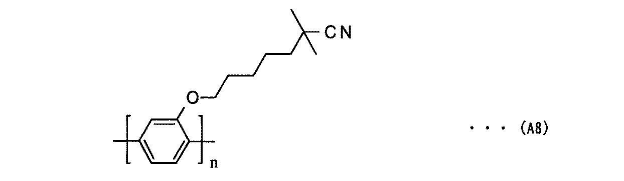
発光層4を構成する高分子材料として、下記式(A8)で示される分子構造を有するポリ[2-(6-シアノ-6-メチルヘプチルオキシ)-1,4-フェニレン](Poly[2-(6-cyano-6-methylheptyloxy)-1,4-phenylene])(以下、CN−PPPと呼ぶ)を用いることができる。CN−PPPの分子量は5,000である。
<CN-PPP>
As a polymer material constituting the light-emitting
<PF8−DMOP>
発光層4を構成する高分子材料として、下記式(A9)で示される分子構造を有するポリ[(9,9-ジオクチルフルオレン-2,7-ジイル)-alt-{1,4-(2,5-ジメトキシ)フェニレン}](Poly[(9,9-dioctylfluorene-2,7-diyl)-alt-{1,4-(2,5-dimethoxy)phenylene}])(以下、PF8−DMOPと呼ぶ)を用いることができる。PF8−DMOPの分子量は160,000である。
<PF8-DMOP>
As a polymer material constituting the light-emitting
<PF8−DSB>
発光層4を構成する高分子材料として、下記式(A10)で示される分子構造を有するポリ[(9,9-ジオクチルフルオレン-2,7-ジイル)-alt-{1,4-ジスチリル-5-(2-エチルヘキシルオキシ)-2-メトキシベンゼン}](Poly[(9,9-dioctylfluorene-2,7-diyl)-alt-{1,4-distyryl-5-(2-ethylhexyloxy)-2-methoxybenzene}])(以下、PF8−DSBと呼ぶ)を用いることができる。PF8−DSBの分子量は56,000である。
<PF8-DSB>
As a polymer material constituting the
<PF6−CNVinyl>
発光層4を構成する高分子材料として、下記式(A11)で示される分子構造を有するポリ(9,9-ジヘキシルフルオレニレン-シアノビニレン)(Poly(9,9-dihexylfluorenylene-cyanovinylene))(以下、PF6−CNVinylと呼ぶ)を用いることができる。PF6−CNVinylの分子量は420,000である。
<PF6-CNVinyl>
As a polymer material constituting the
<PF8−PPV>
発光層4を構成する高分子材料として、下記式(A12)で示される分子構造を有するポリ[(9,9-ジオクチルフルオレン-2,7-ジイル)-alt-(1,4-ジビニレン-フェニレン)](Poly[(9,9-dioctylfluorene-2,7-diyl)-alt-(1,4-divinylene-phenylene)])(以下、PF8−PPVと呼ぶ)を用いることができる。PF8−PPVの分子量は20,000である。
<PF8-PPV>
As a polymer material constituting the
<PF8>
発光層4を構成する高分子材料として、下記式(A13)で示される分子構造を有するポリ(9,9-ジオクチルフルオレン-2,7-ジイル)(Poly(9,9-dioctylfluorene-2,7-diyl))(以下、PF8と呼ぶ)を用いることができる。PF8の分子量は140,000である。
<PF8>
As a polymer material constituting the
<PF6>
発光層4を構成する高分子材料として、下記式(A14)で示される分子構造を有するポリ(9,9-ジヘキシルフルオレン-2,7-ジイル)(Poly(9,9-dihexylfluorene-2,7-diyl))(以下、PF6と呼ぶ)を用いることができる。PF6の分子量は300,000である。
<PF6>
As a polymer material constituting the
<PF6−TPDAB>
発光層4を構成する高分子材料として、下記式(A15)で示される分子構造を有するポリ[(9,9-ジヘキシルフルオレン-2,7-ジイル)-alt−{N,N’-ビス(4-ブチルフェニル)-N,N’-ジフェニル-1,4-ジアミノベンゼン}](Poly[(9,9-dihexylfluorene-2,7-diyl)-alt-{N,N’-bis(4-butylphenyl)-N,N’-diphenyl-1,4-diaminobenzene}])(以下、PF6−TPDABと呼ぶ)を用いることができる。PF6−TPDABの分子量は10,000である。
<PF6-TPDAB>
As a polymer material constituting the
<PF6−Ant>
発光層4を構成する高分子材料として、下記式(A16)で示される分子構造を有するポリ[(9,9-ジヘキシルフルオレン-2,7-ジイル)-alt-(9,10-アントラセン-9,10-ジイル)](Poly[(9,9-dihexylfluoren-2,7-diyl)-alt-(9,10-anthracene-9,10-diyl)])(以下、PF6−Antと呼ぶ)を用いることができる。PF6−Antの分子量は65,000である。
<PF6-Ant>
As a polymer material constituting the
<PF6−Cz>
発光層4を構成する高分子材料として、下記式(A17)で示される分子構造を有するポリ[(9,9-ジヘキシルフルオレン-2,7-ジイル)-alt-(9-エチルカルバゾール-3,6-ジイル)](Poly[(9,9-dihexylfluorene-2,7-diyl)-alt-(9-ethylcarbazole-3,6-diyl)])(以下、PF6−Czと呼ぶ)を用いることができる。PF6−Czの分子量は50,000である。
<PF6-Cz>
As a polymer material constituting the
<PF6−DAP>
発光層4を構成する高分子材料として、下記式(A18)で示される分子構造を有するポリ[(9,9-ジヘキシルフルオレン-2,7-ジイル)-alt-{N,N’-ビス(4-ブチルフェニル)-1,4-ジアミノベンゼン}](Poly[(9,9-dihexylfluorene-2,7-diyl)-alt-{N,N’-bis(4-buthylphenyl)-1,4-diaminobenzene}])(以下、PF6−DAPと呼ぶ)を用いることができる。PF6−DAPの分子量は40,000である。
<PF6-DAP>
As a polymer material constituting the
<Poly−TPD>
発光層4を構成する高分子材料として、下記式(A19)で示される分子構造を有するポリ[N,N’-ビス(4-ブチルフェニル)-N,N’-ジフェニル-1,1’-ビフェニル-4,4’-ジアミン](Poly[N,N’-bis(4-buthylphenyl)-N,N’-diphenyl-1,1’-biphenyl-4,4’-diamine])(以下、Poly−TPDと呼ぶ)を用いることができる。Poly−TPDの分子量は29,000である。
<Poly-TPD>
As a polymer material constituting the
<PF8−Bpy>
発光層4を構成する高分子材料として、下記式(A20)で示される分子構造を有するポリ[(9,9-ジオクチルフルオレン-2,7-ジイル)-alt-{(2,2’-ビピリジン)-6,6’-ジイル}](Poly[(9,9-dioctylfluorene-2,7-diyl)-alt-[(2,2’-bipyridine)-6,6’-diyl}])(以下、PF8−Bpyと呼ぶ)を用いることができる。PF8−Bpyの分子量は10,000である。
<PF8-Bpy>
As a polymer material constituting the
<PF8−Cz>
発光層4を構成する高分子材料として、下記式(A21)で示される分子構造を有するポリ[(9,9-ジオクチルフルオレン-2,7-ジイル)-alt-(9-ブチルカルバゾール-3,6-ジイル)](Poly[(9,9-dioctylfluorene-2,7-diyl)-alt-(9-butylcarbazole-3,6-diyl)])(以下、PF8−Czと呼ぶ)を用いることができる。PF8−Czの分子量は32,000である。
<PF8-Cz>
As a polymer material constituting the
<PVCz>
発光層4を構成する高分子材料として、下記式(A22)で示される分子構造を有するポリ(N-ビニルカルバゾール)(Poly(N-vinylcarbazole))(以下、PVCzと呼ぶ)を用いることができる。PVCzの分子量は1000,000である。
<PVCz>
As a polymer material constituting the
<PF8−SB(10%)>
発光層4を構成する高分子材料として、下記式(A23)で示される分子構造を有する[(9,9-ジオクチルフルオレン-2,7-ジイル):(スチリルベンゼン-4,4’-ジイル)](90:10)共重合体(Poly[(9,9-dioctylfluorene-2,7-diyl)-co-(styrylbenzene)-4,4’-diyl])(以下、PF8−SB(10%)と呼ぶ)を用いることができる。PF8−SB(10%)の分子量は860,000である。
<PF8-SB (10%)>
The polymer material constituting the
<PF8−TPA>
発光層4を構成する高分子材料として、下記式(A24)で示される分子構造を有するポリ[(9,9-ジオクチルフルオレン-2,7-ジイル)-alt-(トリフェニルアミン-4,4’-ジイル)](Poly[(9,9-dioctylfluorene-2,7-diyl)-alt-(triphenylamine-4,4’-diyl)])(以下、PF8−TPAと呼ぶ)を用いることができる。PF8−TPAの分子量は50,000である。
<PF8-TPA>
As a polymer material constituting the
<PF8−TPD>
発光層4を構成する高分子材料として、下記式(A25)で示される分子構造を有するポリ[(9,9-ジオクチクフルオレン-2,7-ジイル)-alt-{N,N’-ビス(4-tert-ブチルフェニル)-N,N’-ジフェニル-1,1’-ビフェニル-4,4’-ジアミン}](Poly[(9,9-dioctylfluorene-2,7-diyl)-alt-{N,N’-bis(4-tert-butylphenyl)-N,N’-diphenyl-1,1’-biphenyl-4,4’-diamine}])(以下、PF8−TPDと呼ぶ)を用いることができる。PF8−TPDの分子量は230,000である。
<PF8-TPD>
As a polymer material constituting the
<PF8−BT(10%)>
発光層4を構成する高分子材料として、下記式(A26)で示される分子構造を有する[(9,9-ジオクチルフルオレン-2,7-ジイル):(ベンゾチオゾール-4,7-ジイル)](90:10)共重合体(Poly[(9,9-dioctylfluorene-2,7-diyl)-co-(benzothiazole-4,7-diyl)])(以下、PF8−BT(10%)と呼ぶ)を用いることができる。PF8−BT(10%)の分子量は440,000である。
<PF8-BT (10%)>
The polymer material constituting the
<PF8−Py>
発光層4を構成する高分子材料として、下記式(A27)で示される分子構造を有するポリ[(9,9-ジオクチルフルオレン-2,7-ジイル)-alt-(ピリジン-2,6-ジイル)](Poly[(9,9-dioctylfluorene-2,7-diyl)-alt-(pyridine-2,6-diyl)])(以下、PF8−Pyと呼ぶ)を用いることができる。PF8−Pyの分子量は97,000である。
<PF8-Py>
As a polymer material constituting the
発光層4を構成する高分子材料は、上記の例に限定されず、他の発光性の高分子材料を用いることもできる。ここで、発光層4を構成する高分子材料は、2種類以上の高分子材料の混合物でもよい。また、1種類または2種類以上の高分子材料に1種類または2種類以上の低分子材料を添加してもよい。
The polymer material constituting the
3種類以上の高分子材料を混合することにより白色発光を得ることも可能となる。 White light emission can be obtained by mixing three or more kinds of polymer materials.
また、発光層4を構成する高分子材料として、電子受容性および電子供与性の両方を有するバイポーラ性の高分子材料を用いることにより、信頼性の向上を図ることができる。バイポーラ性の高分子材料として、例えば、PF6−CVAPを用いることができる。
Further, by using a bipolar polymer material having both electron accepting property and electron donating property as the polymer material constituting the
また、発光層4にMEH−PPV等の単一の繰り返し単位を有する高分子材料を用いた場合、正孔の注入に対しては安定であるが、電子の注入により不安定になる。この場合、バイポーラ性のPF6−CVAPをMEH−PPVに混合することにより、発光層4の電子受容性を高め、結果的に有機電界発光素子の長寿命化を図ることができる。
Further, when a polymer material having a single repeating unit such as MEH-PPV is used for the
図4は有機電界発光素子における正孔注入層、正孔輸送層、発光層、電子輸送層および電子注入層における最低空分子軌道(LUMO)および最高被占分子軌道(HOMO)のエネルギーレベルを示す模式図である。 FIG. 4 shows the energy levels of the lowest unoccupied molecular orbital (LUMO) and highest occupied molecular orbital (HOMO) in the hole injection layer, hole transport layer, light emitting layer, electron transport layer and electron injection layer in the organic electroluminescence device. It is a schematic diagram.
図4において、電子は、陰極から電子注入層および電子輸送層を通して発光層に輸送される。また、正孔は、陽極から正孔注入層および正孔輸送層を通して発光層に輸送される。この場合、正孔輸送層のLUMOレベルが高いと、電子がブロックされる。また、電子輸送層のHOMOレベルが低いと、正孔がブロックされる。それにより、電子および正孔が発光層で結合しやすくなる。 In FIG. 4, electrons are transported from the cathode to the light emitting layer through the electron injection layer and the electron transport layer. Holes are transported from the anode to the light emitting layer through the hole injection layer and the hole transport layer. In this case, electrons are blocked when the LUMO level of the hole transport layer is high. Further, when the HOMO level of the electron transport layer is low, holes are blocked. Thereby, electrons and holes are easily combined in the light emitting layer.
HOMOとLUMOとのエネルギー差で示されるバンドギャップが異なる2つの発光性の高分子材料を混合して発光層に用いる場合、通常、バンドギャップが小さい発光性の高分子材料から発光が得られる。その際に、バンドギャップが小さい高分子材料が発光しない高分子材料からのエネルギー移動を受けることにより、より高い発光効率を得ることができる。 When two light-emitting polymer materials having different band gaps indicated by the energy difference between HOMO and LUMO are mixed and used for the light-emitting layer, light emission is usually obtained from the light-emitting polymer material having a small band gap. At that time, the polymer material having a small band gap receives energy transfer from the polymer material that does not emit light, whereby higher luminous efficiency can be obtained.
表1に上記の発光層4を構成する高分子材料の発光色、発光ピーク波長、吸収ピーク波長、HOMOレベル、バンドギャップ、LUMOレベルおよび分子量の一覧を示す。
Table 1 shows a list of emission colors, emission peak wavelengths, absorption peak wavelengths, HOMO levels, band gaps, LUMO levels, and molecular weights of the polymer materials constituting the
図5は発光層を構成する高分子材料のLUMOレベルおよびHOMOレベルを示す図である。 FIG. 5 is a diagram showing the LUMO level and the HOMO level of the polymer material constituting the light emitting layer.
第1の実施の形態では、電子輸送層5の高分子材料を考慮して発光色、分子量、LUMOレベルおよびHOMOレベルに基づいて高分子材料を選択する。
In the first embodiment, the polymer material is selected based on the emission color, molecular weight, LUMO level, and HOMO level in consideration of the polymer material of the
また、第2および第3の実施の形態では、正孔輸送層8の材料を考慮して発光色、分子量、LUMOレベルおよびHOMOレベルに基づいて高分子材料を選択する。 In the second and third embodiments, the polymer material is selected based on the emission color, molecular weight, LUMO level, and HOMO level in consideration of the material of the hole transport layer 8.
(電子輸送層5の材料)
電子輸送層5を構成する材料としては、発光層4の高分子材料を考慮して上記の表1の高分子材料から選択することができる。この場合、電子輸送層5としては、発光層4よりもLUMOレベルが低い(LUMOレベルの絶対値が大きい)高分子材料を選択する。また、電子輸送層5のHOMOレベルが低い(HOMOレベルの絶対値が大きい)ほど正孔阻止の効果が大きくなる。
(Material of electron transport layer 5)
The material constituting the
電子輸送層5としては、例えばPF8−DSB、MEH−PPV、PF8−MEHPPV、PF8、PF8−Py、PF6−Ant、PF6、PF6−CNVinyl等を用いることができる。
As the
電子輸送層5を構成する高分子材料は、上記の例に限定されず、他の電子輸送性の高分子材料を用いることもできる。ここで、電子輸送層5を構成する高分子材料は、2種類以上の高分子材料の混合物でもよい。また、1種類または2種類以上の高分子材料に1種類または2種類以上の低分子材料を添加してもよい。
The polymer material constituting the
電子輸送層5を構成する高分子材料に添加する低分子材料(低分子電子輸送性材料)としては、次のものが挙げられる。
Examples of the low molecular material (low molecular electron transporting material) added to the polymer material constituting the
<ZnPBO>
低分子電子輸送性添加剤として、下記式(B1)で示される分子構造を有するジンク・ビス{2-(o-ヒドロキシフェニル)ベンゾオキサゾラート}(Zinc bis[2-(o-hydroxyphenyl)benzoxazolate])(以下、ZnPBOと呼ぶ)を用いることができる。ZnPBOの分子量は486である。
<ZnPBO>
As a low molecular weight electron transport additive, zinc bis {2- (o-hydroxyphenyl) benzoxazolate} having a molecular structure represented by the following formula (B1) (Zinc bis [2- (o-hydroxyphenyl) benzoxazolate) ]) (Hereinafter referred to as ZnPBO). The molecular weight of ZnPBO is 486.
<アントラセン>
低分子電子輸送性添加剤として、下記式(B2)で示される分子構造を有するアントラセン(Anthracene)を用いることができる。アントラセンの分子量は178である。
<Anthracene>
As the low molecular electron transport additive, anthracene having a molecular structure represented by the following formula (B2) can be used. The molecular weight of anthracene is 178.
<Alq3>
低分子電子輸送性添加剤として、下記式(B3)で示される分子構造を有するアルミニウム・トリス-(8-キノリノレート)(Aluminum tris-(8-quinolinolate)))(以下、Alq3 と呼ぶ)を用いることができる。Alq3 の分子量は459である。
<Alq3>
Aluminum tris- (8-quinolinolate) (hereinafter referred to as Alq 3 ) having a molecular structure represented by the following formula (B3) as a low molecular electron transport additive Can be used. The molecular weight of Alq 3 is 459.
<ペリレン>
低分子電子輸送性添加剤として、下記式(B4)で示される分子構造を有するペリレン(Perylene)を用いることができる。ペリレンの分子量は252である。
<Perylene>
As the low molecular electron transport additive, perylene having a molecular structure represented by the following formula (B4) can be used. The molecular weight of perylene is 252.
<OXD−7>
低分子電子輸送性添加剤として、下記式(B5)で示される分子構造を有する1,3-ビス[5-(4-tert-ブチルフェニル)-1,3,4-オキサジゾール-2-イル]ベンゼン(1,3-bis[5-(4-tert-butylphenyl)-1,3,4-oxadizol-2-yl]benzen)(以下、OXD−7と呼ぶ)を用いることができる。OXD−7の分子量は478である。
<OXD-7>
1,3-bis [5- (4-tert-butylphenyl) -1,3,4-oxadizol-2-yl] having a molecular structure represented by the following formula (B5) as a low molecular electron transport additive Benzene (1,3-bis [5- (4-tert-butylphenyl) -1,3,4-oxadizol-2-yl] benzen) (hereinafter referred to as OXD-7) can be used. The molecular weight of OXD-7 is 478.
(正孔輸送層8の材料)
正孔輸送層8を構成する材料としては、発光層4の高分子材料を考慮して上記の表1の高分子材料から選択することができる。この場合、正孔輸送層8としては、発光層4よりもHOMOレベルが高い(HOMOレベルの絶対値が小さい)高分子材料を選択する。また、正孔輸送層8のLUMOレベルが高い(LUMOレベルの絶対値が小さい)ほど電子阻止の効果が大きくなる。
(Material of hole transport layer 8)
The material constituting the hole transport layer 8 can be selected from the polymer materials shown in Table 1 in consideration of the polymer material of the
正孔輸送層8としては、例えばPF8−SB、PF8−BT、PVCz等を用いることができる。 As the hole transport layer 8, for example, PF8-SB, PF8-BT, PVCz, or the like can be used.
正孔輸送層8を構成する高分子材料は、上記の例に限定されず、他の正孔輸送性の高分子材料を用いることもできる。ここで、正孔輸送層8を構成する高分子材料は、2種類以上の高分子材料の混合物でもよい。また、1種類または2種類以上の高分子材料に1種類または2種類以上の低分子材料を添加してもよい。 The polymer material constituting the hole transport layer 8 is not limited to the above example, and other hole transport polymer materials can also be used. Here, the polymer material constituting the hole transport layer 8 may be a mixture of two or more kinds of polymer materials. One or two or more kinds of low molecular materials may be added to one kind or two or more kinds of polymer materials.
正孔輸送層8を構成する高分子材料に添加する低分子材料(低分子正孔輸送性材料)としては、次のものが挙げられる。 Examples of the low molecular material (low molecular hole transporting material) added to the polymer material constituting the hole transport layer 8 include the following.
<TPD>
低分子正孔輸送性添加剤として、下記式(B6)で示される分子構造を有するN,N'-ビス-(3-メチルフェニル)-N,N'-ビス-(フェニル)-ベンジジン(N,N'-Bis-(3-methylphenyl)-N,N'-bis-(phenyl)-benzidine)(以下、TPDと呼ぶ)を用いることができる。TPDの分子量は570である。
<TPD>
N, N′-bis- (3-methylphenyl) -N, N′-bis- (phenyl) -benzidine (N) having a molecular structure represented by the following formula (B6) as a low molecular hole transporting additive N'-Bis- (3-methylphenyl) -N, N'-bis- (phenyl) -benzidine) (hereinafter referred to as TPD) can be used. The molecular weight of TPD is 570.
<NPB>
低分子正孔輸送性添加剤として、下記式(B7)で示される分子構造を有するN,N'-ジ(ナフタレン-1-イル)-N,N'-ジフェニル-ベンジジン(N,N'-Di(naphthalen-1-yl)-N,N'-diphenyl-benzidine)(以下、NPBと呼ぶ)を用いることができる。NPBの分子量は644である。
<NPB>
As a low molecular hole transporting additive, N, N′-di (naphthalen-1-yl) -N, N′-diphenyl-benzidine (N, N′-) having a molecular structure represented by the following formula (B7) Di (naphthalen-1-yl) -N, N′-diphenyl-benzidine (hereinafter referred to as NPB) can be used. The molecular weight of NPB is 644.
上記の低分子材料を用いて電子輸送層5または正孔輸送層8を形成してもよい。上記の低分子材料を用いた電子輸送層5または正孔輸送層8の形成方法としては、一般的な真空蒸着法の他に、この低分子材料を有機溶媒に溶解させ、スピンコート法等の湿式法で成膜する方法を用いてもよい。特に、本実施の形態では、湿式法を用いることが好ましい。
The
発光層およびキャリア輸送層に用いることができる高分子材料としては、単一のモノマーから合成された高分子材料の他に、複数のモノマーから合成された共重合体が挙げられる。 Examples of the polymer material that can be used for the light-emitting layer and the carrier transport layer include a polymer synthesized from a plurality of monomers in addition to a polymer material synthesized from a single monomer.
表1には主として2種類のモノマーからなる1対1の共重合体の例を示したが、これに限らず、異なるモノマーを用いた共重合体、1対1以外のモノマー構成比を有する共重合体、または3種類以上のモノマーからなる共重合体を使用することも可能である。 Table 1 shows an example of a one-to-one copolymer mainly composed of two types of monomers. However, the present invention is not limited to this, and a copolymer using different monomers and a copolymer having a monomer composition ratio other than one-to-one. It is also possible to use a polymer or a copolymer composed of three or more types of monomers.
共重合体の設計指針としては、べ一スとなる高分子骨格に、類似の形状を有するモノマーを適当な配合比で結合させたり、キャリア輸送性(電子輸送性または正孔輸送性)を補助するモノマーを適当な配合比で結合させたり、発光性の高いモノマーを適当な配合比で結合させたり、またはキャリア輸送性および発光性の両方を有するモノマーを適当な配合比で結合させることにより、高分子材料の性能を向上させる方法が用いられる。 As a design guideline for the copolymer, a monomer having a similar shape is bonded to the base polymer skeleton at an appropriate blending ratio, and carrier transportability (electron transportability or hole transportability) is assisted. By combining monomers to be mixed at an appropriate mixing ratio, bonding monomers having high light-emitting properties at an appropriate mixing ratio, or combining monomers having both carrier transporting properties and light-emitting properties at an appropriate mixing ratio, A method for improving the performance of the polymer material is used.
キャリア輸送性モノマーでは、配合比が1モル%から70モル%の範囲、特に3モル%から50モル%の範囲にある場合に高い性能向上の効果が得られる。 With the carrier transporting monomer, a high performance improvement effect is obtained when the blending ratio is in the range of 1 mol% to 70 mol%, particularly in the range of 3 mol% to 50 mol%.
また、発光性モノマーでは、配合比が0.2モル%から50モル%の範囲、特に0.5モル%から30モル%の範囲にある場合に高い性能向上の効果が得られる。 In the case of the luminescent monomer, a high performance improvement effect can be obtained when the blending ratio is in the range of 0.2 mol% to 50 mol%, particularly in the range of 0.5 mol% to 30 mol%.
発光性またはキャリア輸送性を発現するモノマーとしては、パイ電子を有するアリール基、ベンゼン、ナフタレン、アントラセン、ピレン、ナフタセン、トリフェニレン、ペリレン、フェナントレン、スチリルベンゼン、ジスチリルベンゼン、フルオレン、ビフェニル等の芳香族炭化水素化合物またはこれらに種々の置換基が付加された化合物、チオフェン、ベンゾチオフェン、ピロール、ポルフィリン、オキサゾール、ベンズオキサゾール、オキサジアゾール、チアゾール、ベンズチアゾール、ベンズチジアゾール、ピラゾリン、トリアゾール、シロキサン、カルバゾール、ピリジン、フェニルピリジン、ピリミジン、ピラジン、トリアジン、オキサジン、キノリン、キナゾリン、キナクリドン、チアジン、ベンゾフラン、クマリン、クロメン、ベンゾフラン、キサンテン、チオキサンテン、アクリジン、チオニン、フェナジン、フェノキサジン、フェナントロリン等のヘテロ環化合物またはこれらに種々の置換基が付加された化合物、フェニルアミン、ナフチルアミン、トリフェニルアミン、アゾベンゼン等の窒素含有化合物またはこれらに種々の置換基が付加された化合物、フェニルシラン等のシリコン含有化合物等を用いることができる。 Monomers that exhibit light-emitting properties or carrier transport properties include aromatic groups such as aryl groups having pi electrons, benzene, naphthalene, anthracene, pyrene, naphthacene, triphenylene, perylene, phenanthrene, styrylbenzene, distyrylbenzene, fluorene, and biphenyl. Hydrocarbon compounds or compounds with various substituents added thereto, thiophene, benzothiophene, pyrrole, porphyrin, oxazole, benzoxazole, oxadiazole, thiazole, benzthiazole, benzthiazole, pyrazoline, triazole, siloxane, carbazole , Pyridine, phenylpyridine, pyrimidine, pyrazine, triazine, oxazine, quinoline, quinazoline, quinacridone, thiazine, benzofuran, coumarin, chloro Heterocyclic compounds such as benzene, benzofuran, xanthene, thioxanthene, acridine, thionine, phenazine, phenoxazine, and phenanthroline, or compounds having various substituents added thereto, nitrogen such as phenylamine, naphthylamine, triphenylamine, and azobenzene A compound containing a compound or various substituents added thereto, a silicon-containing compound such as phenylsilane, or the like can be used.
高分子材料の分子量は、材料合成の際の反応条件(反応温度、反応時間、モノマー配合比、触媒濃度、原料濃度、反応溶媒等)を調整することにより制御することが可能である。また、精製条件(分液、カラムクロマトグラフィー、再沈殿等)を調整することにより不純物、触媒、未反応モノマー、低分子量成分等の不要物を取り除くことができるので、一定の分子量を有する高分子材料を得ることができる。 The molecular weight of the polymer material can be controlled by adjusting the reaction conditions (reaction temperature, reaction time, monomer blending ratio, catalyst concentration, raw material concentration, reaction solvent, etc.) during material synthesis. In addition, impurities such as impurities, catalysts, unreacted monomers, and low molecular weight components can be removed by adjusting purification conditions (separation, column chromatography, reprecipitation, etc.), so a polymer having a certain molecular weight Material can be obtained.
ここで、発光層4の形成に使用される有機溶媒は二種類以上の有機溶媒からなる混合溶媒でもよい。
Here, the organic solvent used for forming the
発光層4の形成に使用される有機溶媒としては、例えば、エチルセロソルブ、メチルセロソルブ、トルエン、o−ジクロロベンゼン、2,2−ジメチルブタン、2,4−ジメチルペンタン、2−メチルヘキサン、3−メチルヘキサン、2,2,4−トリメチルペンタン、2−メチルブタン、2,2、5−トリメチルヘキサン、1,1,2−トリクロロ−1,2,2−トリフルオロエタン、1−ペンテン、2,2,3−トリメチルペンタン、2−メチルペンタン、n−ペンタン、trans−2−ペンテン、1−ヘキセン、cis−2−ペンテン、2−クロロ−2−メチルプロパン、1,1,2,2−テトラクロロ−1,2−ジフルオロエタン、1−へプテン、ヘキサン、n−オクタン、1−オクテン、ヘプタン、n−ノナン、1−ノネン、n−デカン、1−クロロペンタン、1−デセン、2−クロロブタン、ベンゾトリフルオリド、メチルシクロヘキサン、メチルシクロペンタン、2−クロロプロパン、メシチレン、1−クロロブタン、エチルシクロヘキサン、p−キシレン、m−キシレン、2−ブロモプロパン、シクロヘキセン、シクロペンタン、1−クロロプロパン、シクロヘキサン、2,3−ジメチルブタン、o−キシレン、テトラクロロメタン、ヘキサフルオロベンゼン、ペンタクロロエタン、1−クロロ−2−メチルプロパン、1,1−ジクロロエチレン、1,1,1,2−テトラクロロエタン、1,1,1−トリクロロエタン、1−ブロモプロパン、クメン、p−クロロトルエン、ジエチルスルファイド、o−クロロトルエン、p−ジクロロベンゼン、1,1−ジクロロエタン、テトラクロロエチレン、m−ジクロロベンゼン、p−ジエチルベンゼン、m−ジエチルベンゼン、エチルベンゼン、トリクロロエチレン、3−クロロプロペン、o−ジエチルベンゼン、o−ジクロロベンゼン、ブロモエタン、トルエン、クロロベンゼン、トリクロロメタン、フルオロベンゼン、1,2−ジクロロエチレン(trans)、1,1,2,2−テトラクロロエタン、1.2−ジクロロプロパン、ベンゼン、1,2,3−トリクロロプロパン、スチレン、イソブチロニトリル、1,2−ジクロロエチレン(cis)、1−ブロモ−2−クロロエタン、1,2−ジクロロエタン、ヘキサクロロエチレン、1,2−ジブロモエタン、1,1,2−トリクロロエタン、ジクロロメタン、バレロニトリル、チオフェン、カーボンジスルァイド、クロロブロモメタン、ブロモベンゼン、2−ニトロプロパン、1−ニトロプロパン、ベンゾニトリル、ニトロエタン等炭化水素、ハロゲン化炭化水素、ニトロ化炭化水素、ニトリル類等から選択された1種または2種以上の混合溶媒を用いることができる。 Examples of the organic solvent used for forming the light emitting layer 4 include ethyl cellosolve, methyl cellosolve, toluene, o-dichlorobenzene, 2,2-dimethylbutane, 2,4-dimethylpentane, 2-methylhexane, 3- Methylhexane, 2,2,4-trimethylpentane, 2-methylbutane, 2,2,5-trimethylhexane, 1,1,2-trichloro-1,2,2-trifluoroethane, 1-pentene, 2,2 , 3-trimethylpentane, 2-methylpentane, n-pentane, trans-2-pentene, 1-hexene, cis-2-pentene, 2-chloro-2-methylpropane, 1,1,2,2-tetrachloro -1,2-difluoroethane, 1-heptene, hexane, n-octane, 1-octene, heptane, n-nonane, 1-nonene, n Decane, 1-chloropentane, 1-decene, 2-chlorobutane, benzotrifluoride, methylcyclohexane, methylcyclopentane, 2-chloropropane, mesitylene, 1-chlorobutane, ethylcyclohexane, p-xylene, m-xylene, 2-bromo Propane, cyclohexene, cyclopentane, 1-chloropropane, cyclohexane, 2,3-dimethylbutane, o-xylene, tetrachloromethane, hexafluorobenzene, pentachloroethane, 1-chloro-2-methylpropane, 1,1-dichloroethylene, 1,1,1,2-tetrachloroethane, 1,1,1-trichloroethane, 1-bromopropane, cumene, p-chlorotoluene, diethylsulfide, o-chlorotoluene, p-dichlorobenzene, 1,1-dichloro Ethane, tetrachloroethylene, m-dichlorobenzene, p-diethylbenzene, m-diethylbenzene, ethylbenzene, trichloroethylene, 3-chloropropene, o-diethylbenzene, o-dichlorobenzene, bromoethane, toluene, chlorobenzene, trichloromethane, fluorobenzene, 1,2 -Dichloroethylene (trans), 1,1,2,2-tetrachloroethane, 1.2-dichloropropane, benzene, 1,2,3-trichloropropane, styrene, isobutyronitrile, 1,2-dichloroethylene (cis) 1-bromo-2-chloroethane, 1,2-dichloroethane, hexachloroethylene, 1,2-dibromoethane, 1,1,2-trichloroethane, dichloromethane, valeronitrile, thiophene, carbondi One or more selected from hydrocarbons such as sulfide, chlorobromomethane, bromobenzene, 2-nitropropane, 1-nitropropane, benzonitrile, nitroethane, halogenated hydrocarbons, nitrated hydrocarbons, nitriles, etc. The mixed solvent can be used.
キャリア輸送層の形成に使用される有機溶媒は二種類以上の有機溶媒からなる混合溶媒でもよい。 The organic solvent used for forming the carrier transport layer may be a mixed solvent composed of two or more kinds of organic solvents.
キャリア輸送層(電子輸送層5または正孔輸送層8)の形成に使用される有機溶媒としは、例えば、エチルセロソルブ、メチルセロソルブ、トルエン、o−ジクロロベンゼン、2,2−ジメチルブタン、2,4−ジメチルペンタン、2−メチルヘキサン、3−メチルヘキサン、2,2,4−トリメチルペンタン、2−メチルブタン、2,2、5−トリメチルヘキサン、1,1,2−トリクロロ−1,2,2−トリフルオロエタン、1−ペンテン、2,2,3−トリメチルペンタン、2−メチルペンタン、n−ペンタン、trans−2−ペンテン、1−ヘキセン、cis−2−ペンテン、2−クロロ−2−メチルプロパン、1,1,2,2−テトラクロロ−1,2−ジフルオロエタン、1−へプテン、ヘキサン、n−オクタン、1−オクテン、ヘプタン、n−ノナン、1−ノネン、n−デカン、1−クロロペンタン、1−デセン、2−クロロブタン、ベンゾトリフルオリド、メチルシクロヘキサン、メチルシクロペンタン、2−クロロプロパン、メシチレン、1−クロロブタン、エチルシクロヘキサン、p−キシレン、m−キシレン、2−ブロモプロパン、シクロヘキセン、シクロペンタン、1−クロロプロパン、シクロヘキサン、2,3−ジメチルブタン、o−キシレン、テトラクロロメタン、ヘキサフルオロベンゼン、ペンタクロロエタン、1−クロロ−2−メチルプロパン、1,1−ジクロロエチレン、1,1,1,2−テトラクロロエタン、1,1,1−トリクロロエタン、1−ブロモプロパン、クメン、p−クロロトルエン、ジエチルスルファイド、o−クロロトルエン、p−ジクロロベンゼン、1,1−ジクロロエタン、テトラクロロエチレン、m−ジクロロベンゼン、p−ジエチルベンゼン、m−ジエチルベンゼン、エチルベンゼン、トリクロロエチレン、3−クロロプロペン、o−ジエチルベンゼン、o−ジクロロベンゼン、ブロモエタン、トルエン、クロロベンゼン、トリクロロメタン、フルオロベンゼン、1,2−ジクロロエチレン(trans)、1,1,2,2−テトラクロロエタン、1.2−ジクロロプロパン、ベンゼン、1,2,3−トリクロロプロパン、スチレン、イソブチロニトリル、1,2−ジクロロエチレン(cis)、1−ブロモ−2−クロロエタン、1,2−ジクロロエタン、ヘキサクロロエチレン、1,2−ジブロモエタン、1,1,2−トリクロロエタン、ジクロロメタン、バレロニトリル、チオフェン、カーボンジスルァイド、クロロブロモメタン、ブロモベンゼン、2−ニトロプロパン、1−ニトロプロパン、ベンゾニトリル、ニトロエタン等、炭化水素、ハロゲン化炭化水素、ニトロ化炭化水素、ニトリル類等から選択された1種または2種以上の混合溶媒を用いることができる。 Examples of the organic solvent used for forming the carrier transport layer (electron transport layer 5 or hole transport layer 8) include, for example, ethyl cellosolve, methyl cellosolve, toluene, o-dichlorobenzene, 2,2-dimethylbutane, 2, 4-dimethylpentane, 2-methylhexane, 3-methylhexane, 2,2,4-trimethylpentane, 2-methylbutane, 2,2,5-trimethylhexane, 1,1,2-trichloro-1,2,2 -Trifluoroethane, 1-pentene, 2,2,3-trimethylpentane, 2-methylpentane, n-pentane, trans-2-pentene, 1-hexene, cis-2-pentene, 2-chloro-2-methyl Propane, 1,1,2,2-tetrachloro-1,2-difluoroethane, 1-heptene, hexane, n-octane, 1-octene Heptane, n-nonane, 1-nonene, n-decane, 1-chloropentane, 1-decene, 2-chlorobutane, benzotrifluoride, methylcyclohexane, methylcyclopentane, 2-chloropropane, mesitylene, 1-chlorobutane, ethylcyclohexane P-xylene, m-xylene, 2-bromopropane, cyclohexene, cyclopentane, 1-chloropropane, cyclohexane, 2,3-dimethylbutane, o-xylene, tetrachloromethane, hexafluorobenzene, pentachloroethane, 1-chloro 2-methylpropane, 1,1-dichloroethylene, 1,1,1,2-tetrachloroethane, 1,1,1-trichloroethane, 1-bromopropane, cumene, p-chlorotoluene, diethylsulfide, o-chloro toluene p-dichlorobenzene, 1,1-dichloroethane, tetrachloroethylene, m-dichlorobenzene, p-diethylbenzene, m-diethylbenzene, ethylbenzene, trichloroethylene, 3-chloropropene, o-diethylbenzene, o-dichlorobenzene, bromoethane, toluene, chlorobenzene, Trichloromethane, fluorobenzene, 1,2-dichloroethylene (trans), 1,1,2,2-tetrachloroethane, 1.2-dichloropropane, benzene, 1,2,3-trichloropropane, styrene, isobutyronitrile 1,2-dichloroethylene (cis), 1-bromo-2-chloroethane, 1,2-dichloroethane, hexachloroethylene, 1,2-dibromoethane, 1,1,2-trichloroethane, dichloromethane, From valeronitrile, thiophene, carbon disulfide, chlorobromomethane, bromobenzene, 2-nitropropane, 1-nitropropane, benzonitrile, nitroethane, hydrocarbons, halogenated hydrocarbons, nitrated hydrocarbons, nitriles, etc. One or two or more selected mixed solvents can be used.
また、発光層4を構成する高分子材料を選択することにより、発光層4からの発光色を調整することができる。
In addition, the color of light emitted from the
発光層4を異なる発光色を発生する2層の発光層により形成してもよい。例えば、2層の発光層のうち一方に橙色〜赤色発光を得ることが可能な高分子材料を用い、他方に青色発光を得ることが可能な高分子材料を用いることにより、白色発光を得ることができる。この場合、白色発光を得ることが可能な有機電界発光素子に赤色、緑色および青色のフィルタを組み合わせることにより光の3原色の表示(RGB表示)が可能となり、フルカラー表示が実現する。
The
また、緑色発光する発光層を備えた有機電界発光素子、橙色または赤色発光する発光層を備えた有機電界発光素子および青色発光する発光層を備えた有機電界発光素子を組み合わせて用いてもよい。この場合、橙色または赤色発光する有機電界発光素子を赤色に発光する画素(R画素)として用い、緑色発光する有機電界発光素子を緑色に発光する画素(G画素)として用い、青色発光する有機電界発光素子を青色に発光する画素(B画素)として用いることにより、光の3原色の表示(RGB表示)が可能となり、フルカラー表示が実現する。 In addition, an organic electroluminescent element having a green emitting layer, an organic electroluminescent element having an orange or red emitting layer, and an organic electroluminescent element having a blue emitting layer may be used in combination. In this case, an organic electroluminescent element that emits orange or red light is used as a pixel that emits red light (R pixel), an organic electroluminescent element that emits green light is used as a pixel that emits green light (G pixel), and an organic electric field that emits blue light is used. By using the light emitting element as a pixel that emits blue light (B pixel), it is possible to display the three primary colors of light (RGB display), thereby realizing full color display.
以下の実施例では、上記実施の形態に係る有機電界発光素子を作製し、発光特性および発光寿命を評価した。 In the following examples, the organic electroluminescence device according to the above embodiment was manufactured, and the light emission characteristics and the light emission lifetime were evaluated.
(実施例1)
実施例1では、図1に示した三層構造を有する有機電界発光素子を次の方法により作製した。
Example 1
In Example 1, the organic electroluminescent element having the three-layer structure shown in FIG. 1 was produced by the following method.
実施例1の有機電界発光素子の製造方法について説明する。ITOからなる陽極2を備えた基板1を用いた。まず、陽極2上に、下記式(D1)で示される分子構造を有する[2,3−ジヒドロチエノ(3,4,−b)(1,4)ジオキシン−5,7−ジイル]のポリ(p−スチレンスルホン酸)塩とポリ(p−スチレンスルホン酸)の混合物ポリ(エチレンジオキシチオフェン):ポリ(スチレンスルホナート)(Poly(ethylenedioxythiophene):Poly(styrenesulphonate))(以下、PEDOT:PSSという)をスピンコート法により40nmの膜厚を有するように形成し、180℃で10分間大気中においてベークすることにより正孔注入層3を形成した。
The manufacturing method of the organic electroluminescent element of Example 1 will be described. A
次に、正孔注入層3上に、MEH−PPVをスピンコート法により40nmの膜厚を有するように形成し、窒素雰囲気中において80℃で5分間ベークすることにより発光層4を形成した。この際、MEH−PPVはo−ジクロロベンゼン(比誘電率6.828)溶液として用いた。
Next, MEH-PPV was formed on the
続いて、発光層4上に、PF8−DSBをスピンコート法により40nmの膜厚を有するように形成することにより、正孔阻止層を兼ねる電子輸送層5を形成した。この際、PF8−DSBは、トルエン(比誘電率2.283)溶液として用いた。電子輸送層5は、発光層4の高分子膜を損傷することなく形成された。
Subsequently, PF8-DSB was formed on the
電子輸送層5上に、膜厚6nmのカルシウムからなる電子注入層6および膜厚200nmのアルミニウムからなる陰極7を真空蒸着法により形成した。
An
(比較例1)
比較例1では、図1に示す二層構造を有する有機電界発光素子を次の方法により作製した。
(Comparative Example 1)
In Comparative Example 1, an organic electroluminescent element having a two-layer structure shown in FIG. 1 was produced by the following method.
実施例1と同様に、ITOからなる陽極2を備えた基板1を用いた。まず、実施例1と同様に、陽極2上に、PEDOT:PSSをスピンコート法により40nmの膜厚を有するように形成し、180℃で10分間大気中においてベークすることにより正孔注入層3を形成した。
Similarly to Example 1, the
次に、実施例1と同様に、正孔注入層3上に、MEH−PPVをスピンコート法により40nmの膜厚を有するように形成し、窒素雰囲気中において80℃で5分間ベークすることにより発光層4を形成した。この際、MEH−PPVはo−ジクロロベンゼン溶液として用いた。
Next, as in Example 1, MEH-PPV was formed on the
発光層4上に、膜厚6nmのカルシウムからなる電子注入層6および膜厚200nmのアルミニウムからなる陰極7を真空蒸着法により形成した。
On the
(評価1)
実施例1および比較例1の有機電界発光素子の発光効率を測定した。実施例1および比較例1の有機電界発光素子における発光層4および電子輸送層5の材料、発光効率および輝度半減寿命の測定結果を表2に示す。
(Evaluation 1)
Luminous efficiency of the organic electroluminescent elements of Example 1 and Comparative Example 1 was measured. Table 2 shows the measurement results of materials, light emission efficiency, and luminance half-life of the
表2において、各高分子材料の分子量を括弧内に示す。 In Table 2, the molecular weight of each polymer material is shown in parentheses.
表2に示すように、三層構造を有する実施例1の有機電界発光素子は、二層構造を有する比較例1の有機電界発光素子よりも高い発光効率を有することがわかった。 As shown in Table 2, it was found that the organic electroluminescent element of Example 1 having a three-layer structure had higher luminous efficiency than the organic electroluminescent element of Comparative Example 1 having a two-layer structure.
また、実施例1および比較例1の有機電界発光素子の信頼性試験を行った。図7は信頼性試験の結果を示す図である。図7の横軸は時間を表し、縦軸は輝度を表す。 Moreover, the reliability test of the organic electroluminescent element of Example 1 and Comparative Example 1 was performed. FIG. 7 is a diagram showing the results of the reliability test. The horizontal axis in FIG. 7 represents time, and the vertical axis represents luminance.
この信頼性試験においては、有機電界発光素子の初期輝度が240cd/m2となるように電流を調整し、有機電界発光素子を定電流で駆動し、輝度半減寿命を測定した。実施例1の有機電界発光素子の電流は0.28mAであり、比較例1の有機電界発光素子の電流は3.00mAであった。素子面積は2.8mm2である。 In this reliability test, the current was adjusted so that the initial luminance of the organic electroluminescent device was 240 cd / m 2 , the organic electroluminescent device was driven at a constant current, and the luminance half life was measured. The current of the organic electroluminescent element of Example 1 was 0.28 mA, and the current of the organic electroluminescent element of Comparative Example 1 was 3.00 mA. The element area is 2.8 mm 2 .
図7に示すように、比較例1の有機電界発光素子の輝度半減寿命は400時間であった。これに対して、実施例1の有機電界発光素子の輝度半減寿命は3800時間以上であった。それにより、三層構造を有する実施例1の有機電界発光素子では、二層構造を有する比較例1の有機電界発光素子に比べて輝度半減寿命を大幅に改善できることがわかった。 As shown in FIG. 7, the luminance half life of the organic electroluminescent element of Comparative Example 1 was 400 hours. On the other hand, the luminance half life of the organic electroluminescent element of Example 1 was 3800 hours or more. Thereby, it was found that the luminance half-life of the organic electroluminescent element of Example 1 having a three-layer structure can be significantly improved as compared with the organic electroluminescent element of Comparative Example 1 having a two-layer structure.
(比較例2)
比較例2では、図1に示した三層構造を有する有機電界発光素子を次の方法により作製した。
(Comparative Example 2)
In Comparative Example 2, an organic electroluminescent element having the three-layer structure shown in FIG. 1 was produced by the following method.
実施例1と同様に、ITOからなる陽極2を備えた基板1を用いた。まず、実施例1と同様に、陽極2上に、PEDOT:PSSをスピンコート法により40nmの膜厚を有するように形成し、180℃で10分間大気中においてベークすることにより正孔注入層3を形成した。
Similarly to Example 1, the
次に、正孔注入層3上に、PF6−CVAPをスピンコート法により40nmの膜厚を有するように形成し、窒素雰囲気中において80℃で5分間ベークすることにより発光層4を形成した。この際、PF6−CVAPはo−ジクロロベンゼン溶液として用いた。
Next, PF6-CVAP was formed on the
続いて、発光層4上に、MEH−PPVを40nmの膜厚を有するようにスピンコート法により形成することにより、電子輸送層5を形成した。この際、MEH−PPVはトルエン溶液として用いた。電子輸送層5は、発光層4の高分子膜を損傷することなく形成された。
Subsequently, the
電子輸送層5上に、膜厚6nmのカルシウムからなる電子注入層6および膜厚200nmのアルミニウムからなる陰極7を真空蒸着法により形成した。
An
発光層4を構成する高分子材料の繰り返し単位および電子輸送層5を構成する高分子材料の繰り返し単位には同一の骨格(フェニレンビニレン骨格)が含まれる。
The repeating unit of the polymer material constituting the
(実施例2)
実施例2では、図1に示した三層構造を有する有機電界発光素子を次の方法より作製した。
(Example 2)
In Example 2, the organic electroluminescent element having the three-layer structure shown in FIG. 1 was produced by the following method.
実施例1と同様に、ITOからなる陽極2を備えたガラス基板1を用いた。まず、実施例1と同様に、陽極2上に、PEDOT:PSSをスピンコート法により40nmの膜厚を有するように形成し、180℃で10分間大気中においてベークすることにより正孔注入層3を形成した。
As in Example 1, the
次に、正孔注入層3上に、PF6−CVAPをスピンコート法により40nmの膜厚を有するように形成し、窒素雰囲気中において80℃で5分間ベークすることにより発光層4を形成した。この際、PF6−CVAPはo−ジクロロベンゼン溶液として用いた。
Next, PF6-CVAP was formed on the
続いて、発光層4上に、PF8−DSBを40nmの膜厚を有するようにスピンコート法により形成することにより、正孔阻止層を兼ねる電子輸送層5を形成した。この際、PF8−DSBはトルエン溶液として用いた。電子輸送層5は、発光層4の高分子膜を損傷することなく形成された。
Subsequently, PF8-DSB was formed on the
電子輸送層5上に、膜厚6nmのカルシウムからなる電子注入層6および膜厚200nmのアルミニウムからなる陰極7を真空蒸着法により形成した。
An
(評価2)
実施例2および比較例2の有機電界発光素子の発光効率を測定した。実施例2および比較例2の有機電界発光素子における発光層4および電子輸送層5の材料および発光効率の測定結果を表3に示す。
(Evaluation 2)
The luminous efficiencies of the organic electroluminescent elements of Example 2 and Comparative Example 2 were measured. Table 3 shows the materials of the
表3に示すように、下層である発光層4を構成する材料の分子量が上層である電子輸送層5を構成する材料の分子量よりも大きい実施例2の有機電界発光素子は、下層である発光層4を構成する材料の分子量が上層である電子輸送層5を構成する材料の分子量よりも小さい比較例2の有機電界発光素子よりも高い発光効率を有することがわかった。
As shown in Table 3, the organic electroluminescent element of Example 2 in which the molecular weight of the material constituting the lower
また、電子輸送層5を構成する材料が電子輸送性に加えて正孔阻止性を有する実施例2の有機電界発光素子は、電子輸送層5を構成する材料が正孔阻止性を有さない比較例2の有機電界発光素子よりも高い発光効率を有することがわかった。
Further, in the organic electroluminescent element of Example 2 in which the material constituting the
図8は実施例2の有機電界発光素子における正孔注入層3、発光層4および電子輸送層5における最低空分子軌道(LUMO)および最高被占分子軌道(HOMO)のエネルギーレベルを示す模式図である。また、図9は比較例2の有機電界発光素子の正孔注入層3、発光層4および電子輸送層5における最低空分子軌道(LUMO)および最高被占分子軌道(HOMO)のエネルギーレベルを示す模式図である。
FIG. 8 is a schematic diagram showing the energy levels of the lowest unoccupied molecular orbital (LUMO) and the highest occupied molecular orbital (HOMO) in the
図8に示すように、実施例2の有機電界発光素子においては、発光層4のHOMOのエネルギーレベルは−5.33eVとなり、電子輸送層5のHOMOのエネルギーレベルは−5.17eVとなる。これに対して、図9に示すように、比較例2の有機電界発光素子においては、正孔注入層3のHOMOのエネルギーレベルは−5.33eVとなり、電子輸送層5のHOMOのエネルギーレベルは−5.57eVとなる。
As shown in FIG. 8, in the organic electroluminescent element of Example 2, the HOMO energy level of the
それにより、実施例2の有機電界発光素子では、正孔注入層3から発光層4に注入された正孔が発光層4と電子輸送層5との間でのエネルギー障壁により陰極7側に通り抜けることが阻止される。したがって、発光層4において電子と正孔とのバランスが適正となり、電子と正孔とが効率よく再結合する。その結果、高い発光効率が得られる。
Thereby, in the organic electroluminescent element of Example 2, holes injected from the
なお、従来の2層型有機電界発光素子では、正孔輸送層と発光層の2層を形成することが限度であったため、正孔が過剰に発光層内に流れ込み、電子の注入が正孔の注入に追いつかない。それにより、電子と正孔とのバランスが適正に取れないため、本来得られるべき発光効率よりも低い発光効率しか得られない。 In the conventional two-layer type organic electroluminescent device, since it was the limit to form two layers of a hole transport layer and a light emitting layer, holes would flow excessively into the light emitting layer, and injection of electrons would result in hole injection. Can't catch up with the injection. As a result, the balance between electrons and holes cannot be properly obtained, so that only a light emission efficiency lower than the light emission efficiency that should be originally obtained can be obtained.
(実施例3)
実施例3では、発光層4および電子輸送層5の膜厚を変えて9種類の有機電界発光素子を作製し、発光特性を評価した。実施例3の有機電界発光素子の構造および作製方法は、発光層4および電子輸送層5の膜厚を除いて実施例1の有機電界発光素子と同様である。
(Example 3)
In Example 3, nine types of organic electroluminescent elements were produced by changing the film thickness of the
表4に、9種類の有機電界発光素子1−1,1−2,1−3,2−1,2−2,2−3,3−1,3−2,3−3の発光層4および電子輸送層5の膜厚を示す。
Table 4 shows the
(評価3)
実施例3の9種類の有機電界発光素子の発光効率を測定した。実施例3の9種類の有機電界発光素子1−1,1−2,1−3,2−1,2−2,2−3,3−1,3−2,3−3の発光効率の測定結果を表5に示す。
(Evaluation 3)
The luminous efficiency of the nine types of organic electroluminescent elements of Example 3 was measured. The nine types of organic electroluminescent elements 1-1, 1-2, 1-3, 2-1, 2-2, 2-3, 3-1, 3-2, 3-3 of Example 3 Table 5 shows the measurement results.
表5に示すように、有機電界発光素子1−2,1−3,2−2,2−3のように電子輸送層5の膜厚および発光層4の膜厚が実施例1と異なる場合でも、比較例1および比較例2の有機電界発光素子と比べて高い発光効率が得られることがわかった。
As shown in Table 5, when the film thickness of the
(実施例4)
実施例4では、実施例2と同じ構造の有機電界発光素子を実施例2と同じ方法で作製した。
Example 4
In Example 4, an organic electroluminescent element having the same structure as in Example 2 was produced in the same manner as in Example 2.
(実施例5)
実施例5では、図1に示した三層構造を有する有機電界発光素子を次の方法により作製した。発光層4は2種類の高分子材料から構成される。
(Example 5)
In Example 5, an organic electroluminescent element having the three-layer structure shown in FIG. 1 was produced by the following method. The
実施例1と同様に、ITOからなる陽極2を備えた基板1を用いた。まず、実施例1と同様に、陽極2上に、PEDOT:PSSをスピンコート法により40nmの膜厚を有するように形成し、180℃で10分間大気中においてベークすることにより正孔注入層3を形成した。
Similarly to Example 1, the
次に、正孔注入層3上に、MEH−PPVにPF6−CVAPを10wt%添加したものをスピンコート法により40nmの膜厚を有するように形成し、窒素雰囲気中において80℃で5分間ベークすることにより発光層4を形成した。この際、発光層4を構成する高分子はo−ジクロロベンゼン溶液として用いた。
Next, 10 wt% of PF6-CVAP added to MEH-PPV is formed on the
続いて、発光層4上に、PF8−DSBを40nmの膜厚を有するようにスピンコート法により形成することにより、正孔阻止層を兼ねる電子輸送層5を形成した。この際、PF8−DSBはトルエン溶液として用いた。電子輸送層5は、発光層4の高分子膜を損傷することなく形成された。
Subsequently, PF8-DSB was formed on the
正孔阻止層を兼ねる電子輸送層5上に、膜厚6nmのカルシウムからなる電子注入層6および膜厚200nmのアルミニウムからなる陰極7を真空蒸着法により形成した。
An
(評価4)
実施例4,5の有機電界発光素子の輝度半減寿命を測定した。実施例4,5の有機電界発光素子における発光層4および電子輸送層5の材料および輝度半減寿命の測定結果を表6に示す。測定条件としては、初期輝度が200cd/m2であり、室温で定電流駆動を行った。素子面積は2.8mm2である。
(Evaluation 4)
The luminance half lives of the organic electroluminescent elements of Examples 4 and 5 were measured. Table 6 shows the materials of the
表6に示すように、発光層4が2種類の高分子材料から構成される実施例5の有機電界発光素子は、発光層4が1種類の高分子材料から構成される実施例4の有機電界発光素子よりも長い輝度半減寿命を有することがわかった。
As shown in Table 6, the organic electroluminescence device of Example 5 in which the
特に、発光層4の材料としてMEH−PPVにPF6−CVAPを添加したものを用いた有機電界発光素子にあっては、発光層4の材料としてMEH−PPVを単独で用いた有機電界発光素子よりも輝度半減寿命が2倍になり、輝度半減寿命を大幅に向上できることがわかった。
In particular, in an organic electroluminescent device using MEH-PPV with PF6-CVAP added as the material of the
(実施例6)
実施例6では、実施例1の有機電界発光素子と同様の構造を有する有機電界発光素子を実施例1と同様の方法により作製した。
(Example 6)
In Example 6, an organic electroluminescent element having the same structure as that of the organic electroluminescent element of Example 1 was produced by the same method as in Example 1.
(実施例7)
実施例7では、図1に示した三層構造を有する有機電界発光素子を次の方法により作製した。電子輸送層5は2種類の高分子材料から構成される。
(Example 7)
In Example 7, an organic electroluminescent element having the three-layer structure shown in FIG. 1 was produced by the following method. The
実施例1と同様に、ITOからなる陽極2を備えたガラス基板1を用いた。まず、実施例1と同様に、陽極2上に、PEDOT:PSSをスピンコート法により40nmの膜厚を有するように形成し、180℃で10分間大気中においてベークすることにより正孔注入層3を形成した。
As in Example 1, the
次に、正孔注入層3上に、MEH−PPVををスピンコート法により40nmの膜厚を有するように形成し、窒素雰囲気中において80℃で5分間ベークすることにより発光層4を形成した。この際、発光層4を構成する高分子はo−ジクロロベンゼン溶液として用いた。
Next, MEH-PPV was formed on the
続いて、発光層4上に、PF8−DSBにZnBTZを5wt%添加したものを40nmの膜厚を有するようにスピンコート法により形成することにより、正孔阻止層を兼ねる電子輸送層5を形成した。この際、電子輸送層5を構成する高分子材料はトルエン溶液として用いた。電子輸送層5は、発光層4の高分子膜を損傷することなく形成された。
Subsequently, an
電子輸送層5上に、膜厚6nmのカルシウムからなる電子注入層6および膜厚200nmのアルミニウムからなる陰極7を真空蒸着法により形成した。
An
(評価5)
実施例6,7の有機電界発光素子の発光効率を測定した。実施例6,7の有機電界発光素子における発光層4および電子輸送層5の材料および発光効率の測定結果を表7に示す。
(Evaluation 5)
The luminous efficiency of the organic electroluminescent elements of Examples 6 and 7 was measured. Table 7 shows the materials of the
表7に示すように、電子輸送層5が2種類の材料から構成される実施例7の有機電界発光素子は、電子輸送層5が1種類の高分子材料から構成される実施例6の有機電界発光素子よりも高い発光効率を有することがわかった。
As shown in Table 7, the organic electroluminescent device of Example 7 in which the
特に、電子輸送層5の材料としてPF8−DSBにZnBTZを添加したものを用いた有機電界発光素子にあっては、電子輸送層5の材料としてPF8−DSBを単独で用いた有機電界発光素子よりも発光効率が大幅に向上することがわかった。
In particular, in an organic electroluminescent device using a material obtained by adding ZnBTZ to PF8-DSB as a material for the
(実施例8)
実施例8では、図1に示した三層構造を有する有機電界発光素子を次の方法により作製した。
(Example 8)
In Example 8, the organic electroluminescent element having the three-layer structure shown in FIG. 1 was produced by the following method.
実施例1と同様に、ITOからなる陽極2を備えたガラス基板1を用いた。まず、実施例1と同様に、陽極2上に、PEDOT:PSSをスピンコート法により40nmの膜厚を有するように形成し、180℃で10分間大気中においてベークすることにより正孔注入層3を形成した。
As in Example 1, the
次に、正孔注入層3上に、MEH−PPVををスピンコート法により40nmの膜厚を有するように形成し、窒素雰囲気中において80℃で5分間ベークすることにより発光層4を形成した。この際、発光層4を構成する高分子はo−ジクロロベンゼン溶液として用いた。
Next, MEH-PPV was formed on the
続いて、発光層4上に、PF8−MEHPPVを40nmの膜厚を有するようにスピンコート法により形成することにより、正孔阻止層を兼ねる電子輸送層5を形成した。この際、電子輸送層5を構成する高分子材料はトルエン溶液として用いた。電子輸送層5は、発光層4の高分子膜を損傷することなく形成された。
Subsequently, PF8-MEHPPV was formed on the
電子輸送層5上に、膜厚6nmのカルシウムからなる電子注入層6および膜厚200nmのアルミニウムからなる陰極7を真空蒸着法により形成した。
An
発光層4を構成する高分子材料の繰り返し単位および電子輸送層5を構成する高分子材料の繰り返し単位には同一の骨格(フェニレンビニレン骨格)が含まれる。
The repeating unit of the polymer material constituting the
(実施例9)
実施例9では、図1に示した三層構造を有する有機電界発光素子を次の方法により作製した。
Example 9
In Example 9, the organic electroluminescent element having the three-layer structure shown in FIG. 1 was produced by the following method.
実施例1と同様に、ITOからなる陽極2を備えたガラス基板1を用いた。まず、実施例1と同様に、陽極2上に、PEDOT:PSSをスピンコート法により40nmの膜厚を有するように形成し、180℃で10分間大気中においてベークすることにより正孔注入層3を形成した。
As in Example 1, the
次に、正孔注入層3上に、MEH−PPVををスピンコート法により40nmの膜厚を有するように形成し、窒素雰囲気中において80℃で5分間ベークすることにより発光層4を形成した。この際、発光層4を構成する高分子はo−ジクロロベンゼン溶液として用いた。
Next, MEH-PPV was formed on the
続いて、発光層4上に、PF8を40nmの膜厚を有するようにスピンコート法により形成することにより、正孔阻止層を兼ねる電子輸送層5を形成した。この際、電子輸送層5を構成する高分子材料はトルエン溶液として用いた。電子輸送層5は、発光層4の高分子膜を損傷することなく形成された。
Subsequently, PF8 was formed on the light-emitting
電子輸送層5上に、膜厚6nmのカルシウムからなる電子注入層6および膜厚200nmのアルミニウムからなる陰極7を真空蒸着法により形成した。
An
発光層4を構成する高分子材料の繰り返し単位および電子輸送層5を構成する高分子材料の繰り返し単位には同一の骨格が含まれない。
The repeating unit of the polymer material constituting the
(実施例10)
実施例10では、図1に示した三層構造を有する有機電界発光素子を次の方法により作製した。
(Example 10)
In Example 10, the organic electroluminescent element having the three-layer structure shown in FIG. 1 was produced by the following method.
実施例1と同様に、ITOからなる陽極2を備えたガラス基板1を用いた。まず、実施例1と同様に、陽極2上に、PEDOT:PSSをスピンコート法により40nmの膜厚を有するように形成し、180℃で10分間大気中においてベークすることにより正孔注入層3を形成した。
As in Example 1, the
次に、正孔注入層3上に、MEH−PPVををスピンコート法により40nmの膜厚を有するように形成し、窒素雰囲気中において80℃で5分間ベークすることにより発光層4を形成した。この際、発光層4を構成する高分子はo−ジクロロベンゼン溶液として用いた。
Next, MEH-PPV was formed on the
続いて、発光層4上に、PF8−Pyを40nmの膜厚を有するようにスピンコート法により形成することにより、正孔阻止層を兼ねる電子輸送層5を形成した。この際、電子輸送層5を構成する高分子材料はトルエン溶液として用いた。電子輸送層5は、発光層4の高分子膜を損傷することなく形成された。
Subsequently, PF8-Py was formed on the
電子輸送層5上に、膜厚6nmのカルシウムからなる電子注入層6および膜厚200nmのアルミニウムからなる陰極7を真空蒸着法により形成した。
An
発光層4を構成する高分子材料の繰り返し単位および電子輸送層5を構成する高分子材料の繰り返し単位には同一の骨格が含まれない。
The repeating unit of the polymer material constituting the
(評価6)
実施例8,9,10の有機電界発光素子の発光効率を測定した。実施例8,9,10の有機電界発光素子における発光層4および電子輸送層5の材料および発光効率の測定結果を表8に示す。
(Evaluation 6)
The luminous efficiency of the organic electroluminescent elements of Examples 8, 9, and 10 was measured. Table 8 shows the materials of the
表8に示すように、電子輸送層5を構成する材料としてPF8−MEHPPV、PF8またはPF8−Pyを用いた実施例8,9,10の有機電界発光素子においても、発光層4の材料の分子量が電子輸送層5の材料の分子量よりも大きいことにより、電子輸送層5の材料としてPF8−DSBを用いた実施例1と同様に高い発光効率が得られることがわかった。
As shown in Table 8, also in the organic electroluminescent elements of Examples 8, 9, and 10 using PF8-MEHPPV, PF8, or PF8-Py as the material constituting the
また、電子輸送層5を構成する材料が電子輸送性に加えて正孔阻止性を有する実施例8,9,10の有機電界発光素子は、電子輸送層5を構成する材料が正孔阻止性を有さない比較例2の有機電界発光素子よりも高い発光効率を有することがわかった。
In addition, in the organic electroluminescent elements of Examples 8, 9, and 10 in which the material constituting the
さらに、発光層4を構成する高分子材料の繰り返し単位と電子輸送層5を構成する高分子材料の繰り返し単位とに同一の骨格(フェニレンビニレン骨格)が含まれる実施例8有機電界発光素子は、発光層4を構成する高分子材料の繰り返し単位と電子輸送層5を構成する高分子材料の繰り返し単位とに同一の骨格が含まれない実施例9,10の有機電界発光素子よりも高い発光効率を有することがわかった。
Furthermore, Example 8 organic electroluminescent element in which the same skeleton (phenylene vinylene skeleton) is contained in the repeating unit of the polymer material constituting the
(実施例11)
実施例11では、図1に示した三層構造を有する有機電界発光素子を次の方法により作製した。
(Example 11)
In Example 11, the organic electroluminescent element having the three-layer structure shown in FIG. 1 was produced by the following method.
実施例1と同様に、ITOからなる陽極2を備えたガラス基板1を用いた。まず、実施例1と同様に、陽極2上に、PEDOT:PSSをスピンコート法により40nmの膜厚を有するように形成し、180℃で10分間大気中においてベークすることにより正孔注入層3を形成した。
As in Example 1, the
次に、正孔注入層3上に、PF8−MEHPPVををスピンコート法により40nmの膜厚を有するように形成し、窒素雰囲気中において80℃で5分間ベークすることにより発光層4を形成した。この際、発光層4を構成する高分子はo−ジクロロベンゼン溶液として用いた。
Next, PF8-MEHPPV was formed on the
続いて、発光層4上に、PF8−DSBを40nmの膜厚を有するようにスピンコート法により形成することにより、正孔阻止層を兼ねる電子輸送層5を形成した。この際、電子輸送層5を構成する高分子材料はトルエン溶液として用いた。電子輸送層5は、発光層4の高分子膜を損傷することなく形成された。
Subsequently, PF8-DSB was formed on the
電子輸送層5上に、膜厚6nmのカルシウムからなる電子注入層6および膜厚200nmのアルミニウムからなる陰極7を真空蒸着法により形成した。
An
(評価7)
実施例11の有機電界発光素子の発光効率を測定した。実施例11の有機電界発光素子における発光層4および電子輸送層5の材料および発光効率の測定結果を表9に示す。
(Evaluation 7)
The luminous efficiency of the organic electroluminescent element of Example 11 was measured. Table 9 shows the materials of the
表9に示すように、発光層4を構成する材料としてPF8−MEHPPVを用いた実施例11の有機電界発光素子においても、発光層4を構成する材料としてMEH−PPVを用いた実施例1の有機電界発光素子と同様に、発光層4の材料の分子量が電子輸送層5の材料の分子量よりも大きいことにより、高い発光効率が得られることがわかった。
As shown in Table 9, also in the organic electroluminescent element of Example 11 using PF8-MEHPPV as the material constituting the
(実施例12)
実施例12では、図1に示した三層構造を有する有機電界発光素子を次の方法により作製した。発光層4は2種類の高分子材料から構成される。
(Example 12)
In Example 12, the organic electroluminescent element having the three-layer structure shown in FIG. 1 was produced by the following method. The
実施例1と同様に、ITOからなる陽極2を備えた基板1を用いた。まず、実施例1と同様に、陽極2上に、PEDOT:PSSをスピンコート法により40nmの膜厚を有するように形成し、180℃で10分間大気中においてベークすることにより正孔注入層3を形成した。
Similarly to Example 1, the
次に、正孔注入層3上に、MEH−PPVにBDPAP−CNMEHPPVを10wt%添加したものをスピンコート法により40nmの膜厚を有するように形成し、窒素雰囲気中において80℃で5分間ベークすることにより発光層4を形成した。この際、発光層4を構成する高分子はo−ジクロロベンゼン溶液として用いた。
Next, 10 wt% of BDPAP-CNMEHPPV added to MEH-PPV is formed on the
続いて、発光層4上に、PF8−DSBを40nmの膜厚を有するようにスピンコート法により形成することにより、正孔阻止層を兼ねる電子輸送層5を形成した。この際、PF8−DSBはトルエン溶液として用いた。電子輸送層5は、発光層4の高分子膜を損傷することなく形成された。
Subsequently, PF8-DSB was formed on the
正孔阻止層を兼ねる電子輸送層5上に、膜厚6nmのカルシウムからなる電子注入層6および膜厚200nmのアルミニウムからなる陰極7を真空蒸着法により形成した。
An
(比較例3)
比較例3では、図1に示した三層構造を有する有機電界発光素子を次の方法により作製した。発光層4は1種類の高分子材料から構成される。
(Comparative Example 3)
In Comparative Example 3, an organic electroluminescent element having the three-layer structure shown in FIG. 1 was produced by the following method. The
実施例1と同様に、ITOからなる陽極2を備えた基板1を用いた。まず、実施例1と同様に、陽極2上に、PEDOT:PSSをスピンコート法により40nmの膜厚を有するように形成し、180℃で10分間大気中においてベークすることにより正孔注入層3を形成した。
Similarly to Example 1, the
次に、正孔注入層3上に、BDPAP−CNMEHPPVをスピンコート法により40nmの膜厚を有するように形成し、窒素雰囲気中において80℃で5分間ベークすることにより発光層4を形成した。この際、発光層4を構成する高分子はo−ジクロロベンゼン溶液として用いた。
Next, BDPAP-CNMEHPPV was formed on the
続いて、発光層4上に、PF8−DSBを40nmの膜厚を有するようにスピンコート法により形成することにより、正孔阻止層を兼ねる電子輸送層5を形成した。この際、PF8−DSBはトルエン溶液として用いた。電子輸送層5は、発光層4の高分子膜を損傷することなく形成された。
Subsequently, PF8-DSB was formed on the
正孔阻止層を兼ねる電子輸送層5上に、膜厚6nmのカルシウムからなる電子注入層6および膜厚200nmのアルミニウムからなる陰極7を真空蒸着法により形成した。
An
(評価8)
実施例12および比較例3の有機電界発光素子の発光効率を測定した。実施例12および比較例3の有機電界発光素子における発光層4および電子輸送層5の材料および発光効率の測定結果を表10に示す。
(Evaluation 8)
Luminous efficiency of the organic electroluminescent elements of Example 12 and Comparative Example 3 was measured. Table 10 shows the materials of the
表10に示すように、発光層4が2種類の材料から構成される実施例12の有機電界発光素子は、発光層4が1種類の高分子材料から構成される比較例3の有機電界発光素子よりも高い発光効率を有することがわかった。
As shown in Table 10, the organic electroluminescent element of Example 12 in which the
特に、発光層4の材料としてMEH−PPVにBDPAP−CNMEHPPVを10wt%添加したものを用いた有機電界発光素子にあっては、発光層4の材料としてBDPAP−CNMEHPPVを単独で用いた有機電界発光素子よりも発光効率が大幅に向上することがわかった。
In particular, in an organic electroluminescence device using MEH-PPV with 10 wt% of BDPAP-CNMEHPPV as the material of the
また、下層である発光層4を構成する材料のうち少なくとも1種類の材料の分子量が上層である電子輸送層5の材料の分子量よりも大きいことにより、高い発光効率が得られることがわかった。
Further, it was found that a high luminous efficiency can be obtained when the molecular weight of at least one of the materials constituting the
(実施例13)
実施例13では、図2に示した三層構造を有する有機電界発光素子を次の方法により作製した。
(Example 13)
In Example 13, the organic electroluminescent element having the three-layer structure shown in FIG. 2 was produced by the following method.
実施例1と同様に、ITOからなる陽極2を備えた基板1を用いた。まず、実施例1と同様に、陽極2上に、PEDOT:PSSをスピンコート法により40nmの膜厚を有するように形成し、180℃で10分間大気中においてベークすることにより正孔注入層3を形成した。
Similarly to Example 1, the
次に、正孔注入層3上に、PVCzをスピンコート法により25nmの膜厚を有するように形成し、窒素雰囲気中において80℃で5分間ベークすることにより電子阻止層を兼ねる正孔輸送層8を形成した。この際、PVCzはo−ジクロロベンゼン(比誘電率6.828)溶液として用いた。
Next, PVCz is formed on the
次に、正孔輸送層8上に、PF8−SB10%をスピンコート法により70nmの膜厚を有するように形成することにより発光層4を形成した。この際、PF8−SB10%はキシレン(比誘電率2.274〜2.562)溶液として用いた。発光層4は、正孔輸送層8の高分子膜を損傷することなく形成された。
Next, the
続いて、発光層4上に、膜厚6nmのカルシウムからなる電子注入層6および膜厚200nmのアルミニウムからなる陰極7を真空蒸着法により形成した。
Subsequently, an
(実施例14)
実施例14では、図2に示した三層構造を有する有機電界発光素子を次の方法により作製した。
(Example 14)
In Example 14, the organic electroluminescent element having the three-layer structure shown in FIG. 2 was produced by the following method.
実施例1と同様に、ITOからなる陽極2を備えた基板1を用いた。まず、実施例1と同様に、陽極2上に、PEDOT:PSSをスピンコート法により40nmの膜厚を有するように形成し、180℃で10分間大気中においてベークすることにより正孔注入層3を形成した。
Similarly to Example 1, the
次に、正孔注入層3上に、PVCzにPF8−TPAを50wt%添加したものをスピンコート法により25nmの膜厚を有するように形成し、窒素雰囲気中において80℃で5分間ベークすることにより電子阻止層を兼ねる正孔輸送層8を形成した。この際、PVCzはo−ジクロロベンゼン(比誘電率6.828)溶液として用いた。
Next, on the
次に、正孔輸送層8上に、PF8−BT(10%)をスピンコート法により70nmの膜厚を有するように形成することにより発光層4を形成した。この際、PF8−SB(10%)はキシレン(比誘電率2.274〜2.562)溶液として用いた。発光層4は、正孔輸送層8の高分子膜を損傷することなく形成された。
Next, the
続いて、発光層4上に、膜厚6nmのカルシウムからなる電子注入層6および膜厚200nmのアルミニウムからなる陰極7を真空蒸着法により形成した。
Subsequently, an
(比較例4)
比較例4では、図2に示した三層構造を有する有機電界発光素子を次の方法により作製した。
(Comparative Example 4)
In Comparative Example 4, an organic electroluminescent element having the three-layer structure shown in FIG. 2 was produced by the following method.
実施例1と同様に、ITOからなる陽極2を備えた基板1を用いた。まず、実施例1と同様に、陽極2上に、PEDOT:PSSをスピンコート法により40nmの膜厚を有するように形成し、180℃で10分間大気中においてベークすることにより正孔注入層3を形成した。
Similarly to Example 1, the
次に、正孔注入層3上に、PF8−SB(10%)をスピンコート法により70nmの膜厚を有するように形成することにより発光層4を形成した。この際、PF8−SB(10%)はキシレン(比誘電率2.274〜2.562)溶液として用いた。発光層4は、正孔輸送層8の高分子膜を損傷することなく形成された。
Next, the
発光層4上に、膜厚6nmのカルシウムからなる電子注入層6および膜厚200nmのアルミニウムからなる陰極7を真空蒸着法により形成した。
On the
(評価9)
実施例13,14および比較例4の有機電界発光素子の発光効率を測定した。実施例13,14および比較例4の有機電界発光素子における正孔輸送層8および発光層4の材料および発光効率の測定結果を表11に示す。
(Evaluation 9)
The luminous efficiencies of the organic electroluminescent elements of Examples 13 and 14 and Comparative Example 4 were measured. Table 11 shows the measurement results of the materials and luminous efficiencies of the hole transport layer 8 and the
表11に示すように、三層構造を有する実施例13,14の有機電界発光素子は、二層構造を有する比較例4の有機電界発光素子よりも高い発光効率を有することがわかった。 As shown in Table 11, it was found that the organic electroluminescent elements of Examples 13 and 14 having a three-layer structure had higher luminous efficiency than the organic electroluminescent element of Comparative Example 4 having a two-layer structure.
また、下層である正孔輸送層8を構成する1種類または複数種類の材料のうち少なくとも1種類の材料の分子量が上層である発光層4の材料の分子量よりも大きいことにより、高い発光効率が得られることがわかった。
In addition, since the molecular weight of at least one material among the one or a plurality of materials constituting the lower hole transport layer 8 is larger than the molecular weight of the
さらに、正孔輸送層8を構成する材料が正孔輸送性に加えて電子阻止性を有する実施例13,14の有機電界発光素子は、正孔輸送層8を有さない比較例4の有機電界発光素子よりも高い発光効率を有することがわかった。 Furthermore, the organic electroluminescent elements of Examples 13 and 14 in which the material constituting the hole transport layer 8 has an electron blocking property in addition to the hole transport property are the organic materials of Comparative Example 4 that do not have the hole transport layer 8. It was found that it has higher luminous efficiency than the electroluminescent element.
また、正孔輸送層8が2種類の材料から構成される実施例14の有機電界発光素子は、正孔輸送層8が1種類の高分子材料から構成される実施例13の有機電界発光素子よりも高い発光効率を有することがわかった。 Moreover, the organic electroluminescent element of Example 14 in which the hole transport layer 8 is composed of two types of materials is the same as the organic electroluminescent element of Example 13 in which the hole transport layer 8 is composed of one type of polymer material. It was found to have a higher luminous efficiency.
特に、正孔輸送層8の材料としてPVCzにPF8−TPAを50wt%添加したものを用いた有機電界発光素子にあっては、正孔輸送層8の材料としてPVCzを用いた有機電界発光素子よりも発光効率が大幅に向上することがわかった。 In particular, in an organic electroluminescence device using a material in which 50% by weight of PF8-TPA is added to PVCz as a material for the hole transport layer 8, the organic electroluminescence device using PVCz as a material for the hole transport layer 8 is used. It was also found that the luminous efficiency is greatly improved.
(実施例15)
実施例15では、図3に示した三層構造を有する有機電界発光素子を次の方法により作製した。
(Example 15)
In Example 15, an organic electroluminescent element having the three-layer structure shown in FIG. 3 was produced by the following method.
実施例1と同様に、ITOからなる陽極2を備えた基板1を用いた。まず、実施例1と同様に、陽極2上に、PEDOT:PSSをスピンコート法により40nmの膜厚を有するように形成し、180℃で10分間大気中においてベークすることにより正孔注入層3を形成した。
Similarly to Example 1, the
次に、正孔注入層3上に、PVCzをスピンコート法により25nmの膜厚を有するように形成し、窒素雰囲気中において80℃で5分間ベークすることにより電子阻止層を兼ねる正孔輸送層8を形成した。この際、PVCzはo−ジクロロベンゼン(比誘電率6.828)溶液として用いた。
Next, PVCz is formed on the
次に、正孔輸送層8上に、PF8−SB10%をスピンコート法により70nmの膜厚を有するように形成することにより発光層4を形成した。この際、PF8−SB10%はキシレン(比誘電率2.274〜2.562)溶液として用いた。発光層4は、正孔輸送層8の高分子膜を損傷することなく形成された。
Next, the
続いて、発光層4上に、膜厚1nmのフッ化リチウムからなる電子注入層6a、膜厚6nmのカルシウムからなる陰極7aおよび膜厚200nmのアルミニウムからなる保護層9を真空蒸着法により形成した。
Subsequently, an electron injection layer 6a made of lithium fluoride with a thickness of 1 nm, a
(評価10)
実施例15の有機電界発光素子の発光効率を測定した。実施例15の有機電界発光素子における正孔輸送層8および発光層4の材料および発光効率の測定結果を表12に示す。
(Evaluation 10)
The light emission efficiency of the organic electroluminescent element of Example 15 was measured. Table 12 shows the materials of the hole transport layer 8 and the
表12に示すように、電子注入層6aがアルカリ金属であるリチウムを含有する実施例15の有機電界発光素子においては、電子注入性が向上することにより、電子注入層6がカルシウムからなる実施例13の有機電界発光素子よりも高い発光効率を有することがわかった。
As shown in Table 12, in the organic electroluminescence device of Example 15 in which the electron injection layer 6a contains lithium which is an alkali metal, the
(評価)
表13は実施例1〜15および比較例1〜3の有機電界発光素子における上層および下層の材料、上層および下層の材料の分子量、分子量比および発光効率を示す。
(Evaluation)
Table 13 shows the molecular weight, the molecular weight ratio, and the luminous efficiency of the upper layer and lower layer materials, the upper layer and lower layer materials in the organic electroluminescent elements of Examples 1 to 15 and Comparative Examples 1 to 3.
なお、表13において、実施例1〜12および比較例1〜3では、下層は発光層4であり、上層は電子輸送層5であり、実施例13〜15では、下層は正孔輸送層8であり、上層は発光層4である。また、分子量比は、上層の材料の分子量に対する下層の材料の分子量の比である。
In Table 13, in Examples 1 to 12 and Comparative Examples 1 to 3, the lower layer is the
また、図10は実施例1,2,7〜11および比較例2,3の有機電界発光素子における分子量比と発光効率との関係を示す図である。 FIG. 10 is a graph showing the relationship between the molecular weight ratio and the light emission efficiency in the organic electroluminescent devices of Examples 1, 2, 7 to 11 and Comparative Examples 2 and 3.
表13および図10から分子量比が大きい程、発光効率が向上することがわかる。3色の有機電界発光素子を用いたフルカラーディスプレイの要求を満足するためには、発光効率は1.5cd/A以上であることが好ましく、2.0cd/A以上であることがより好ましい。したがって、図10より、分子量比が3.5以上であることが好ましく、6.2以上であることがより好ましい。 It can be seen from Table 13 and FIG. 10 that the larger the molecular weight ratio, the better the luminous efficiency. In order to satisfy the requirement of a full color display using three-color organic electroluminescent elements, the luminous efficiency is preferably 1.5 cd / A or more, and more preferably 2.0 cd / A or more. Therefore, from FIG. 10, the molecular weight ratio is preferably 3.5 or more, and more preferably 6.2 or more.
本発明に係る有機電界発光素子は、種々の表示装置、種々の光源等に利用することができる。 The organic electroluminescent element according to the present invention can be used for various display devices, various light sources, and the like.
1 基板
2 陽極
3 正孔注入層
4 発光層
5 電子輸送層
6,6a 電子注入層
7,7a 陰極
8 正孔輸送層
9 保護層
DESCRIPTION OF
Claims (6)
前記第1の高分子材料と前記第2の高分子材料との内、少なくとも一方は、複数のモノマーからなる共重合体であり、前記第1の高分子材料の繰り返し単位と前記第2の高分子材料の繰り返し単位とは共通の骨格を含むと共に、前記第2の高分子材料の分子量が前記第1の高分子材料の分子量よりも小さいことを特徴とする有機電界発光素子。 A first electrode formed on a substrate, a first organic layer formed of a first polymeric material having a light-emitting property, a second organic layer formed of a second polymeric material having a carrier-transporting property, and Two electrodes in order,
At least one of the first polymer material and the second polymer material is a copolymer composed of a plurality of monomers, and the repeating unit of the first polymer material and the second polymer material An organic electroluminescence device comprising a common skeleton with a repeating unit of a molecular material, wherein the molecular weight of the second polymer material is smaller than the molecular weight of the first polymer material.
第1の高分子材料を第1の有機溶媒に溶解させることにより第1の高分子材料の溶液を作製する工程と、
前記第1の高分子材料の繰り返し単位と共通の繰り返し単位を有するとともに、前記第2の高分子材料の分子量が前記第1の高分子材料の分子量よりも小さい分子量を有する第2の高分子材料を第2の有機溶媒に溶解させることにより第2の高分子材料の溶液を作製する工程と、
前記第1の高分子材料の溶液を用いて前記第1の有機層を形成する工程と、
前記第1の有機層上に前記第2の高分子材料の溶液を用いて前記第2の有機層を形成する工程とを備えたことを特徴とする有機電界発光素子の製造方法。 A first electrode formed on a substrate, a first organic layer formed of a first polymeric material having a light-emitting property, a second organic layer formed of a second polymeric material having a carrier-transporting property, and A method for producing an organic electroluminescent device comprising two electrodes in order,
Producing a solution of the first polymer material by dissolving the first polymer material in the first organic solvent;
A second polymer material having a repeating unit in common with the repeating unit of the first polymer material and having a molecular weight of the second polymer material smaller than the molecular weight of the first polymer material A solution of the second polymer material by dissolving in a second organic solvent;
Forming the first organic layer using a solution of the first polymeric material;
And a step of forming the second organic layer on the first organic layer by using a solution of the second polymer material.
Priority Applications (4)
| Application Number | Priority Date | Filing Date | Title |
|---|---|---|---|
| JP2004055397A JP4683846B2 (en) | 2003-03-31 | 2004-02-27 | Organic electroluminescent device and manufacturing method thereof |
| TW093107241A TWI239220B (en) | 2003-03-31 | 2004-03-18 | Organic electro-luminescence element and method of manufacturing same |
| US10/505,677 US7745015B2 (en) | 2003-03-31 | 2004-03-24 | Organic electroluminescent device and method for manufacturing same |
| PCT/JP2004/004104 WO2004089043A1 (en) | 2003-03-31 | 2004-03-24 | Organic electroluminescent device and method for manufacturing same |
Applications Claiming Priority (2)
| Application Number | Priority Date | Filing Date | Title |
|---|---|---|---|
| JP2003097308 | 2003-03-31 | ||
| JP2004055397A JP4683846B2 (en) | 2003-03-31 | 2004-02-27 | Organic electroluminescent device and manufacturing method thereof |
Publications (2)
| Publication Number | Publication Date |
|---|---|
| JP2004319440A JP2004319440A (en) | 2004-11-11 |
| JP4683846B2 true JP4683846B2 (en) | 2011-05-18 |
Family
ID=33134331
Family Applications (1)
| Application Number | Title | Priority Date | Filing Date |
|---|---|---|---|
| JP2004055397A Expired - Lifetime JP4683846B2 (en) | 2003-03-31 | 2004-02-27 | Organic electroluminescent device and manufacturing method thereof |
Country Status (4)
| Country | Link |
|---|---|
| US (1) | US7745015B2 (en) |
| JP (1) | JP4683846B2 (en) |
| TW (1) | TWI239220B (en) |
| WO (1) | WO2004089043A1 (en) |
Families Citing this family (14)
| Publication number | Priority date | Publication date | Assignee | Title |
|---|---|---|---|---|
| KR100731728B1 (en) * | 2004-08-27 | 2007-06-22 | 삼성에스디아이 주식회사 | Donor substrate for laser transfer and manufacturing method of organic EL device using same |
| US7208757B1 (en) * | 2004-12-23 | 2007-04-24 | Spansion Llc | Memory element with nitrogen-containing active layer |
| DE502005004675D1 (en) * | 2005-12-21 | 2008-08-21 | Novaled Ag | Organic component |
| JP2007242816A (en) * | 2006-03-07 | 2007-09-20 | Toppan Printing Co Ltd | Organic electroluminescence device and manufacturing method thereof |
| JP2008034631A (en) * | 2006-07-28 | 2008-02-14 | Seiko Epson Corp | Organic electroluminescence device and electronic device |
| US20090208776A1 (en) * | 2008-02-19 | 2009-08-20 | General Electric Company | Organic optoelectronic device and method for manufacturing the same |
| KR101460184B1 (en) | 2008-03-03 | 2014-11-11 | 삼성디스플레이 주식회사 | METHOD FOR MANUFACTURING ELECTRONALLY-ELEMENT DEVICE |
| JP2010055864A (en) * | 2008-08-27 | 2010-03-11 | Sumitomo Chemical Co Ltd | Organic electroluminescent device and its manufacturing method |
| JP5732463B2 (en) * | 2009-10-05 | 2015-06-10 | トルン ライティング リミテッドThorn Lighting Limited | Multi-layer organic element |
| KR101137129B1 (en) * | 2010-03-25 | 2012-04-19 | 한남대학교 산학협력단 | New MEH-O-D PU copolymer and its preparation method |
| KR101883739B1 (en) * | 2012-04-04 | 2018-07-31 | 삼성전자주식회사 | Polymer blend, organic light emitting diodes using the same and method for controlling charge mobility of the emitting layer of thereof |
| CN103563118A (en) | 2011-05-27 | 2014-02-05 | 出光兴产株式会社 | Organic electroluminescent element |
| US20180323407A1 (en) * | 2017-05-02 | 2018-11-08 | Shenzhen China Star Optoelectronics Technology Co., Ltd. | Organic light emitting device and a method of fabricating thereof |
| WO2019129015A1 (en) * | 2017-12-26 | 2019-07-04 | Tcl集团股份有限公司 | Thin film and fabrication method therefor and qled device |
Family Cites Families (7)
| Publication number | Priority date | Publication date | Assignee | Title |
|---|---|---|---|---|
| JP3125777B2 (en) * | 1999-01-28 | 2001-01-22 | 日本電気株式会社 | Organic electroluminescence device and panel |
| JP4043135B2 (en) * | 1999-03-29 | 2008-02-06 | 株式会社東芝 | Functional element and multi-component multi-phase polymer molding |
| JP4026740B2 (en) * | 2000-09-29 | 2007-12-26 | 富士フイルム株式会社 | Organic light emitting device material and organic light emitting device using the same |
| JP4040249B2 (en) * | 2000-11-16 | 2008-01-30 | 富士フイルム株式会社 | Light emitting element |
| JP2002299061A (en) | 2001-04-02 | 2002-10-11 | Honda Motor Co Ltd | Organic electroluminescence device |
| JP4783526B2 (en) * | 2001-05-23 | 2011-09-28 | 本田技研工業株式会社 | Organic electroluminescence device |
| JP2003257671A (en) * | 2002-02-28 | 2003-09-12 | Fuji Photo Film Co Ltd | Light emitting device and manufacturing method thereof |
-
2004
- 2004-02-27 JP JP2004055397A patent/JP4683846B2/en not_active Expired - Lifetime
- 2004-03-18 TW TW093107241A patent/TWI239220B/en not_active IP Right Cessation
- 2004-03-24 WO PCT/JP2004/004104 patent/WO2004089043A1/en not_active Ceased
- 2004-03-24 US US10/505,677 patent/US7745015B2/en active Active
Also Published As
| Publication number | Publication date |
|---|---|
| TWI239220B (en) | 2005-09-01 |
| WO2004089043A1 (en) | 2004-10-14 |
| TW200425776A (en) | 2004-11-16 |
| US20050147842A1 (en) | 2005-07-07 |
| US7745015B2 (en) | 2010-06-29 |
| JP2004319440A (en) | 2004-11-11 |
Similar Documents
| Publication | Publication Date | Title |
|---|---|---|
| EP2352363B1 (en) | Organic light-emitting diode and method of manufacturing the same | |
| JP4683846B2 (en) | Organic electroluminescent device and manufacturing method thereof | |
| WO2004003104A1 (en) | Organic electroluminescent element and luminescent device or display including the same | |
| US8212244B2 (en) | Blue organic light emitting device | |
| JP2013110121A (en) | Laminate type organic light-emitting element | |
| JPWO2008120714A1 (en) | Organic electroluminescence device and method for manufacturing the same | |
| US20080012482A1 (en) | Material For An Electroluminescence Element And Electroluminescence Element Using The Same | |
| JP6403108B2 (en) | ORGANIC ELECTROLUMINESCENCE ELEMENT AND LIGHT EMITTING DEVICE HAVING THE ELEMENT | |
| JP4522416B2 (en) | ORGANIC ELECTROLUMINESCENCE ELEMENT, IMAGE DISPLAY DEVICE AND LIGHTING DEVICE EQUIPPED WITH THE SAME, CHARGE TRANSPORT MATERIAL, AND CHARGE TRANSPORT LAYER INCLUDING THE SAME | |
| JP2004207102A (en) | Organic electroluminescence device | |
| JP2005276749A (en) | Organic electroluminescent element | |
| JP4688424B2 (en) | Organic electroluminescent device and manufacturing method thereof | |
| JP2010507224A (en) | Cathode coating | |
| KR20120128483A (en) | Organic light emitting diode device | |
| CN102112518B (en) | Color conversion film comprising conjugated high molecular weight copolymer and multicolor light-emitting organic EL device using the color conversion film | |
| KR100757721B1 (en) | Organic electroluminescent device | |
| KR101428821B1 (en) | Organic EL device | |
| KR102076855B1 (en) | thermal polymerization type hole transport material with high molecular weight and organic light emitting diode using the same | |
| JP2000077187A (en) | Organic electroluminescence device | |
| KR102474308B1 (en) | Thermally activated delayed fluorescence compound containing triazine, and organic light emitting diode having the same | |
| KR101329277B1 (en) | Matrix material for organic electroluminescent devices | |
| JP2001011436A (en) | Organic electroluminescence device | |
| CN120463669A (en) | Organic compound, organic electroluminescent device and display panel | |
| JP2002313573A (en) | Organic electroluminescence device | |
| JP2014017419A (en) | Organic electroluminescent element |
Legal Events
| Date | Code | Title | Description |
|---|---|---|---|
| A621 | Written request for application examination |
Free format text: JAPANESE INTERMEDIATE CODE: A621 Effective date: 20060418 |
|
| A131 | Notification of reasons for refusal |
Free format text: JAPANESE INTERMEDIATE CODE: A131 Effective date: 20071127 |
|
| A521 | Request for written amendment filed |
Free format text: JAPANESE INTERMEDIATE CODE: A523 Effective date: 20080128 |
|
| A02 | Decision of refusal |
Free format text: JAPANESE INTERMEDIATE CODE: A02 Effective date: 20080325 |
|
| A521 | Request for written amendment filed |
Free format text: JAPANESE INTERMEDIATE CODE: A523 Effective date: 20080526 |
|
| A911 | Transfer to examiner for re-examination before appeal (zenchi) |
Free format text: JAPANESE INTERMEDIATE CODE: A911 Effective date: 20080709 |
|
| A912 | Re-examination (zenchi) completed and case transferred to appeal board |
Free format text: JAPANESE INTERMEDIATE CODE: A912 Effective date: 20080912 |
|
| A521 | Request for written amendment filed |
Free format text: JAPANESE INTERMEDIATE CODE: A523 Effective date: 20100614 |
|
| A521 | Request for written amendment filed |
Free format text: JAPANESE INTERMEDIATE CODE: A523 Effective date: 20101118 |
|
| A01 | Written decision to grant a patent or to grant a registration (utility model) |
Free format text: JAPANESE INTERMEDIATE CODE: A01 |
|
| A61 | First payment of annual fees (during grant procedure) |
Free format text: JAPANESE INTERMEDIATE CODE: A61 Effective date: 20110208 |
|
| FPAY | Renewal fee payment (event date is renewal date of database) |
Free format text: PAYMENT UNTIL: 20140218 Year of fee payment: 3 |
|
| R151 | Written notification of patent or utility model registration |
Ref document number: 4683846 Country of ref document: JP Free format text: JAPANESE INTERMEDIATE CODE: R151 |
|
| FPAY | Renewal fee payment (event date is renewal date of database) |
Free format text: PAYMENT UNTIL: 20140218 Year of fee payment: 3 |
|
| EXPY | Cancellation because of completion of term |