JP4665983B2 - Electro-optical device and electronic apparatus - Google Patents
Electro-optical device and electronic apparatus Download PDFInfo
- Publication number
- JP4665983B2 JP4665983B2 JP2008086051A JP2008086051A JP4665983B2 JP 4665983 B2 JP4665983 B2 JP 4665983B2 JP 2008086051 A JP2008086051 A JP 2008086051A JP 2008086051 A JP2008086051 A JP 2008086051A JP 4665983 B2 JP4665983 B2 JP 4665983B2
- Authority
- JP
- Japan
- Prior art keywords
- electro
- panel
- liquid crystal
- optical
- corner
- Prior art date
- Legal status (The legal status is an assumption and is not a legal conclusion. Google has not performed a legal analysis and makes no representation as to the accuracy of the status listed.)
- Active
Links
Images


Classifications
-
- G—PHYSICS
- G02—OPTICS
- G02F—OPTICAL DEVICES OR ARRANGEMENTS FOR THE CONTROL OF LIGHT BY MODIFICATION OF THE OPTICAL PROPERTIES OF THE MEDIA OF THE ELEMENTS INVOLVED THEREIN; NON-LINEAR OPTICS; FREQUENCY-CHANGING OF LIGHT; OPTICAL LOGIC ELEMENTS; OPTICAL ANALOGUE/DIGITAL CONVERTERS
- G02F1/00—Devices or arrangements for the control of the intensity, colour, phase, polarisation or direction of light arriving from an independent light source, e.g. switching, gating or modulating; Non-linear optics
- G02F1/01—Devices or arrangements for the control of the intensity, colour, phase, polarisation or direction of light arriving from an independent light source, e.g. switching, gating or modulating; Non-linear optics for the control of the intensity, phase, polarisation or colour
- G02F1/13—Devices or arrangements for the control of the intensity, colour, phase, polarisation or direction of light arriving from an independent light source, e.g. switching, gating or modulating; Non-linear optics for the control of the intensity, phase, polarisation or colour based on liquid crystals, e.g. single liquid crystal display cells
- G02F1/133—Constructional arrangements; Operation of liquid crystal cells; Circuit arrangements
- G02F1/1333—Constructional arrangements; Manufacturing methods
- G02F1/133308—Support structures for LCD panels, e.g. frames or bezels
- G02F1/133314—Back frames
-
- G—PHYSICS
- G02—OPTICS
- G02F—OPTICAL DEVICES OR ARRANGEMENTS FOR THE CONTROL OF LIGHT BY MODIFICATION OF THE OPTICAL PROPERTIES OF THE MEDIA OF THE ELEMENTS INVOLVED THEREIN; NON-LINEAR OPTICS; FREQUENCY-CHANGING OF LIGHT; OPTICAL LOGIC ELEMENTS; OPTICAL ANALOGUE/DIGITAL CONVERTERS
- G02F1/00—Devices or arrangements for the control of the intensity, colour, phase, polarisation or direction of light arriving from an independent light source, e.g. switching, gating or modulating; Non-linear optics
- G02F1/01—Devices or arrangements for the control of the intensity, colour, phase, polarisation or direction of light arriving from an independent light source, e.g. switching, gating or modulating; Non-linear optics for the control of the intensity, phase, polarisation or colour
- G02F1/13—Devices or arrangements for the control of the intensity, colour, phase, polarisation or direction of light arriving from an independent light source, e.g. switching, gating or modulating; Non-linear optics for the control of the intensity, phase, polarisation or colour based on liquid crystals, e.g. single liquid crystal display cells
- G02F1/133—Constructional arrangements; Operation of liquid crystal cells; Circuit arrangements
- G02F1/1333—Constructional arrangements; Manufacturing methods
- G02F1/133308—Support structures for LCD panels, e.g. frames or bezels
- G02F1/13332—Front frames
-
- G—PHYSICS
- G02—OPTICS
- G02F—OPTICAL DEVICES OR ARRANGEMENTS FOR THE CONTROL OF LIGHT BY MODIFICATION OF THE OPTICAL PROPERTIES OF THE MEDIA OF THE ELEMENTS INVOLVED THEREIN; NON-LINEAR OPTICS; FREQUENCY-CHANGING OF LIGHT; OPTICAL LOGIC ELEMENTS; OPTICAL ANALOGUE/DIGITAL CONVERTERS
- G02F1/00—Devices or arrangements for the control of the intensity, colour, phase, polarisation or direction of light arriving from an independent light source, e.g. switching, gating or modulating; Non-linear optics
- G02F1/01—Devices or arrangements for the control of the intensity, colour, phase, polarisation or direction of light arriving from an independent light source, e.g. switching, gating or modulating; Non-linear optics for the control of the intensity, phase, polarisation or colour
- G02F1/13—Devices or arrangements for the control of the intensity, colour, phase, polarisation or direction of light arriving from an independent light source, e.g. switching, gating or modulating; Non-linear optics for the control of the intensity, phase, polarisation or colour based on liquid crystals, e.g. single liquid crystal display cells
- G02F1/133—Constructional arrangements; Operation of liquid crystal cells; Circuit arrangements
- G02F1/1333—Constructional arrangements; Manufacturing methods
- G02F1/1335—Structural association of cells with optical devices, e.g. polarisers or reflectors
- G02F1/1336—Illuminating devices
-
- G—PHYSICS
- G02—OPTICS
- G02F—OPTICAL DEVICES OR ARRANGEMENTS FOR THE CONTROL OF LIGHT BY MODIFICATION OF THE OPTICAL PROPERTIES OF THE MEDIA OF THE ELEMENTS INVOLVED THEREIN; NON-LINEAR OPTICS; FREQUENCY-CHANGING OF LIGHT; OPTICAL LOGIC ELEMENTS; OPTICAL ANALOGUE/DIGITAL CONVERTERS
- G02F2201/00—Constructional arrangements not provided for in groups G02F1/00 - G02F7/00
- G02F2201/50—Protective arrangements
- G02F2201/503—Arrangements improving the resistance to shock
-
- G—PHYSICS
- G02—OPTICS
- G02F—OPTICAL DEVICES OR ARRANGEMENTS FOR THE CONTROL OF LIGHT BY MODIFICATION OF THE OPTICAL PROPERTIES OF THE MEDIA OF THE ELEMENTS INVOLVED THEREIN; NON-LINEAR OPTICS; FREQUENCY-CHANGING OF LIGHT; OPTICAL LOGIC ELEMENTS; OPTICAL ANALOGUE/DIGITAL CONVERTERS
- G02F2202/00—Materials and properties
- G02F2202/28—Adhesive materials or arrangements
Landscapes
- Physics & Mathematics (AREA)
- Nonlinear Science (AREA)
- Mathematical Physics (AREA)
- Chemical & Material Sciences (AREA)
- Crystallography & Structural Chemistry (AREA)
- General Physics & Mathematics (AREA)
- Optics & Photonics (AREA)
- Liquid Crystal (AREA)
- Devices For Indicating Variable Information By Combining Individual Elements (AREA)
Description
本発明は、電気光学装置および電子機器に関するものである。 The present invention relates to an electro-optical device and an electronic apparatus.
現在、携帯電話機、携帯情報端末機等といった各種の電子機器において、各種の情報を視覚的に表示するための表示部として液晶装置(電気光学装置)が用いられている。このような液晶装置の一例として、液晶パネル(電気光学パネル)と、バックライトと、液晶パネル及びバックライトを収容するためのフレーム(保持部材)とを備えた構造が知られている。 Currently, in various electronic devices such as mobile phones and portable information terminals, liquid crystal devices (electro-optical devices) are used as display units for visually displaying various types of information. As an example of such a liquid crystal device, a structure including a liquid crystal panel (electro-optical panel), a backlight, and a frame (holding member) for housing the liquid crystal panel and the backlight is known.
液晶パネルは、一対の基板と、一方の基板の外周部に沿って一対の基板間に形成されたシール材と、これら一対の基板及びシール材により囲まれた領域に配置された液晶とを有して構成されるものである。液晶パネルを構成する一対の基板のうち一方に設けられた張り出し部上にドライバなどが設けられている。
通常、液晶パネルはバックライトを構成するフレーム内に略全周を貼り付けて保持されていたが、モジュールが落下した際、液晶パネルの角部に応力が集中しやすく、特に一枚ガラスとされた基板の張り出し部にパネル割れが発生しやすかった。 Normally, the liquid crystal panel is held in a frame that constitutes the backlight, with the entire circumference attached, but when the module falls, stress tends to concentrate on the corners of the liquid crystal panel, and it is especially made of single glass. Panel cracks were likely to occur in the overhanging portion of the substrate.
本発明は、上記課題に鑑みてなされたものであり、その目的は、落下時の衝撃によって電気光学パネルが破損することを効果的に防止することを可能とした電気光学装置および電子機器を提供することにある。 SUMMARY An advantage of some aspects of the invention is that it provides an electro-optical device and an electronic apparatus that can effectively prevent an electro-optical panel from being damaged by an impact at the time of dropping. There is to do.
本発明の電気光学装置は、上記課題を解決するために、電気光学パネルと、少なくとも前記電気光学パネルを保持する保持部材と、を有し、前記保持部材は、前記電気光学パネルの周縁部の少なくとも一部を支持する段差部を有し、前記段差部は、少なくとも一部の角部とその近傍において、前記電気光学パネルを支持していないことを特徴とする。 In order to solve the above problems, an electro-optical device according to an aspect of the invention includes an electro-optical panel and a holding member that holds at least the electro-optical panel. It has a step part which supports at least one part, and the said step part does not support the said electro-optical panel in at least one corner | angular part and its vicinity.
このような構成によれば、電気光学パネルを保持する保持部材の段差部が、電気光学パネルの少なくとも一部の角部とその近傍を支持していないため、落下時の衝撃が保持部材から電気光学パネルの角部やその近傍に直接伝わるのを防ぐことができ、電気光学パネルが破損してしまうことを防止することができる。
よって、耐衝撃性に優れた液晶装置を得ることができる。
According to such a configuration, the stepped portion of the holding member that holds the electro-optical panel does not support at least some of the corners of the electro-optical panel and the vicinity thereof. Direct transmission to the corners of the optical panel and the vicinity thereof can be prevented, and damage to the electro-optical panel can be prevented.
Therefore, a liquid crystal device excellent in impact resistance can be obtained.
また、前記保持部材が、前記電気光学パネルの側面に対向する側壁部と、前記側壁部の内側に形成された段差部とからなることも好ましい。
このような構成によれば、落下時におけるパネル破損を防止しつつ電気光学パネルを保持部材において良好に保持することができる。
Further, it is preferable that the holding member includes a side wall portion facing the side surface of the electro-optical panel and a step portion formed inside the side wall portion.
According to such a configuration, the electro-optical panel can be satisfactorily held by the holding member while preventing damage to the panel at the time of dropping.
また、電気光学パネルが一対の基板からなり、当該一対の基板のうち一方の基板は他方の基板とは重ならない張り出し部を有し、前記電気光学パネルは、前記一方の基板側から前記段差部に支持され、前記段差部が、前記張り出し部を支持していないことも好ましい。
このような構成によれば、段差部が電気光学パネルの張り出し部を支持しないので、落下時の衝撃が保持部材を介して上記張り出し部に直接伝わることを防止することができる。一枚基板である張り出し部は、基板同士が重なり合う他の領域に比べて衝撃に弱いが、段差部から離れた状態で保持されるので、保持部材から張り出し部に応力が加わることを避けることができる。
The electro-optical panel includes a pair of substrates, and one of the pair of substrates has an overhanging portion that does not overlap the other substrate, and the electro-optical panel includes the stepped portion from the one substrate side. It is also preferable that the step portion does not support the overhang portion.
According to such a configuration, since the step portion does not support the overhanging portion of the electro-optical panel, it is possible to prevent an impact at the time of dropping from being directly transmitted to the overhanging portion via the holding member. The overhanging part, which is a single substrate, is less susceptible to impact than other areas where the substrates overlap, but is held away from the stepped part, so it is possible to avoid applying stress from the holding member to the overhanging part. it can.
また、段差部は、前記張り出し部と重なる領域以外に位置する前記角部とその近傍において、前記電気光学パネルを支持していないことも好ましい。
このような構成によれば、電気光学パネルの四隅(4つの角部とその近傍)が保持部材によって支持されないため、これらの箇所に保持部材からの応力が集中することを防止して電気光学パネルが破損してしまうことを阻止することができる。
Further, it is also preferable that the step portion does not support the electro-optical panel in the corner portion located in a region other than the region overlapping the projecting portion and in the vicinity thereof.
According to such a configuration, since the four corners (four corners and the vicinity thereof) of the electro-optical panel are not supported by the holding member, it is possible to prevent the stress from the holding member from concentrating on these portions and to prevent the electro-optical panel from being concentrated. Can be prevented from being damaged.
また、段差部は、前記少なくとも一部の角部とその近傍において、前記電気光学パネルと接する領域よりも低く形成されていることも好ましい。
このような構成によれば、段差部における少なくとも一部の角部とその近傍が電気光学パネルには接しない(支持しない)ことになるため、落下時の衝撃が保持部材を介して電気光学パネルに伝わることを防止することができる。また、保持部材の少なくとも一部の角部とその近傍に段差部が形成されていない場合よりも、保持部材の強度が向上する。
Further, it is also preferable that the stepped portion is formed lower than the region in contact with the electro-optical panel in the at least some corners and the vicinity thereof.
According to such a configuration, at least a part of the corners in the stepped portion and the vicinity thereof do not contact (not support) the electro-optical panel, so that an impact at the time of dropping is applied to the electro-optical panel via the holding member. Can be prevented from being transmitted to. In addition, the strength of the holding member is improved as compared with the case where the step portion is not formed in at least some corners of the holding member and in the vicinity thereof.
また、段差部は、前記少なくとも一部の角部とその近傍において、前記電気光学パネルと接する領域から前記角部の頂点にかけて低くなる傾斜面を有していることも好ましい。
このような構成によれば、電気光学パネルと接する領域から角部にかけて低くなる傾斜面を有することにより、電気光学パネルと接する領域よりも角部の頂部の方が低くなるので、電気光学パネルの角部に対して段差部の角部が最も離れた状態となるので、落下時の衝撃が段差部(保持部材)を介して電気光学パネルの角部に伝わることを防止することができる。
In addition, it is preferable that the stepped portion has an inclined surface that becomes lower from the region in contact with the electro-optical panel to the apex of the corner in the at least some corners and the vicinity thereof.
According to such a configuration, by having an inclined surface that is lowered from the region in contact with the electro-optical panel to the corner, the top of the corner is lower than the region in contact with the electro-optical panel. Since the corner portion of the step portion is farthest from the corner portion, it is possible to prevent an impact at the time of dropping from being transmitted to the corner portion of the electro-optical panel via the step portion (holding member).
また、前記傾斜面が形成された前記段差部の延在方向において、前記傾斜面の斜面上端が、前記段差部と平行に延びる前記電気光学パネルのシール材の前記角部側の端部よりも、前記保持部材の前記角部から離れた側に位置することも好ましい。
このような構成によれば、落下時の衝撃が、保持部材を介して電気光学パネルのシール材の外側の領域に伝わることを防止することができる。電気光学パネルのシール材の外側の領域は各基板の周縁部であることから相互間には何も介在しておらず、シール材の内側の領域よりも破損しやすい。そこで、本発明は、傾斜面が形成された段差部の延在方向において、傾斜面の斜面上端が、段差部と平行に延びる電気光学パネルのシール材の角部側の端部よりも、保持部材の角部から離れた側に位置するようにした。これにより、電気光学パネルのシール材の外側の領域(すなわち基板の周縁部)に対して落下時の衝撃が保持部材を介して伝わることを確実に防止することができるので、電気光学パネルの破損を阻止することが可能となる。
Further, in the extending direction of the stepped portion where the inclined surface is formed, the upper end of the inclined surface of the inclined surface is more than the end portion on the corner portion side of the sealing material of the electro-optical panel extending in parallel with the stepped portion. It is also preferable that the holding member is located on the side away from the corner.
According to such a configuration, it is possible to prevent an impact at the time of dropping from being transmitted to a region outside the sealing material of the electro-optical panel via the holding member. Since the area outside the sealing material of the electro-optic panel is the peripheral edge of each substrate, nothing is interposed between them, and the area is more easily damaged than the area inside the sealing material. Therefore, the present invention holds the slope upper end of the sloped surface in the extending direction of the stepped portion where the sloped surface is formed, rather than the end portion on the corner side of the sealing material of the electro-optic panel extending in parallel with the stepped portion. It was made to be located on the side away from the corner of the member. As a result, it is possible to reliably prevent the impact at the time of dropping from being transmitted to the region outside the sealing material of the electro-optical panel (that is, the peripheral portion of the substrate) through the holding member. Can be prevented.
また、段差部には、前記少なくとも一部の角部とその近傍に衝撃緩和部材が設けられていることも好ましい。
このような構成によれば、段差部における少なくとも一部の角部とその近傍に衝撃緩和部材が設けられているので、例えば、落下時に保持部材が撓んで電気光学パネルに接触するようなことを防止することができる。また、保持部材と電気光学パネルとの間に衝撃緩和部材を介在させておくことで保持部材自体の撓みも抑制することが可能である。
It is also preferable that the stepped portion is provided with an impact relaxation member at least in the corner portion and in the vicinity thereof.
According to such a configuration, since the impact mitigating member is provided in at least a part of the corner portion in the step portion and the vicinity thereof, for example, when the holding member is bent, the holding member is bent and contacts the electro-optical panel. Can be prevented. Further, it is possible to suppress the bending of the holding member itself by interposing the impact relaxation member between the holding member and the electro-optical panel.
また、保持部材の前記電気光学パネルを支持していない領域においては、前記段差部が形成されていないことも好ましい。
このような構成によれば、落下時の衝撃が保持部材を介して電気光学パネルに伝わることを完全になくすことができる。また、保持部材全体の軽量化を実現でき、且つ放熱性が高まる。
It is also preferable that the stepped portion is not formed in a region of the holding member that does not support the electro-optical panel.
According to such a configuration, it is possible to completely prevent the impact at the time of dropping from being transmitted to the electro-optical panel via the holding member. Moreover, weight reduction of the whole holding member can be implement | achieved and heat dissipation is improved.
また、段差部の前記電気光学パネルを支持する領域が、両面接着部材で構成されていることも好ましい。
このような構成によれば、段差部における電気光学パネルを支持する領域が両面接着部材で構成されているため、電気光学パネルを保持部材に接着固定できるのと同時に両面接着部材によって落下時の衝撃が緩和される。この両面接着部材によって、落下時の衝撃が保持部材を介して電気光学パネルに直接伝わることがなくなるので電気光学パネルの破損を防止することができる。
Moreover, it is also preferable that the area | region which supports the said electro-optical panel of a level | step-difference part is comprised with the double-sided adhesive member.
According to such a structure, since the area | region which supports the electro-optical panel in a level | step-difference part is comprised by the double-sided adhesive member, the electro-optical panel can be adhesively fixed to a holding member, and simultaneously the impact at the time of a fall by a double-sided adhesive member Is alleviated. By this double-sided adhesive member, the impact at the time of dropping is not directly transmitted to the electro-optical panel via the holding member, so that the electro-optical panel can be prevented from being damaged.
本発明の電子機器は、上記のような耐衝撃性に優れた液晶装置を備えていることから、高信頼性を確保した電子機器を得ることができる。 Since the electronic device of the present invention includes the liquid crystal device having excellent impact resistance as described above, an electronic device with high reliability can be obtained.
以下、図面を参照しながら本発明の実施の形態について説明する。なお、以下の図面においては、図面を見やすくするため、各構成要素の膜厚や寸法の比率などは適宜異ならせてある。 Hereinafter, embodiments of the present invention will be described with reference to the drawings. In the following drawings, the film thicknesses and dimensional ratios of the respective components are appropriately changed in order to make the drawings easy to see.
(液晶装置)
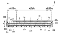
以下に、本発明に係る電気光学装置の一実施形態として液晶装置を例に挙げて説明する。図1は本実施形態における液晶装置の分解斜視図である。図2は、本実施形態における液晶装置の要部を示す断面図であって、図1のA−Aで示す部分の液晶装置の断面図である。図3は、フレームの概略構成を示す平面図であって、図4(a)および(b)はフレームの要部を拡大して示す斜視図、図5(a)および(b)はフレームの傾斜面を示す斜視図、図6は液晶パネルとフレームの傾斜面との位置関係を示す平面図である。
(Liquid crystal device)
Hereinafter, a liquid crystal device will be described as an example of an electro-optical device according to an embodiment of the invention. FIG. 1 is an exploded perspective view of the liquid crystal device according to the present embodiment. FIG. 2 is a cross-sectional view showing a main part of the liquid crystal device in the present embodiment, and is a cross-sectional view of the liquid crystal device at a portion indicated by AA in FIG. FIG. 3 is a plan view showing a schematic configuration of the frame. FIGS. 4A and 4B are enlarged perspective views showing the main part of the frame. FIGS. 5A and 5B are views of the frame. FIG. 6 is a plan view showing the positional relationship between the liquid crystal panel and the inclined surface of the frame.
図1に示すように、液晶装置1(電気光学装置)は、液晶パネル100(電気光学パネル)と、当該液晶パネル100に接続された駆動用FPC(Flexible Printed Circuit)基板10と、液晶パネル100の裏面側に配置されるバックライト200(照明装置)と、液晶パネル100及びバックライト200を収容するフレーム300(保持部材)とを有する。さらに、本実施形態の液晶装置1は、液晶パネル100を駆動させる駆動用FPC基板10の他に、バックライト200の光源とされるLED12を複数備えた光源用FPC基板18を有している。
As shown in FIG. 1, the liquid crystal device 1 (electro-optical device) includes a liquid crystal panel 100 (electro-optical panel), a driving FPC (Flexible Printed Circuit)
液晶パネル100は、図2に示されるように、第1基板3と、第1基板3から張り出した張り出し部2aを有する第2基板2と、これら第1基板3及び第2基板2を貼り合わせるための基板周縁部に設けられたシール材52と、第1基板3及び第2基板2とシール材52とにより形成された空間内に配置された電気光学材料としての液晶層50と、一対の基板2,3を挟むように設けられた第1偏光板8a及び第2偏光板8bとを有している。第1基板3及び第2基板2は、透光性を有するガラス、プラスチック等によって形成されている。
As shown in FIG. 2, the
第2基板2の第1基板3と対向する面上には、ITO(Indium・Tin Oxide)膜からなる複数の画素電極9と、画素電極9を覆うようにポリイミドなどからなる配向膜が形成されている。一方、第1基板3の第2基板2と対向する面上には、ITO膜からなる対向電極21が設けられ、この対向電極21を覆うようにポリイミドなどからなる配向膜が形成されている。ここで、画素電極9、対向電極21及びこれらを覆う配向膜は公知の技術で形成されるもので、図2においてはいずれも図示を省略してある。
A plurality of pixel electrodes 9 made of an ITO (Indium / Tin Oxide) film and an alignment film made of polyimide or the like are formed so as to cover the pixel electrodes 9 on the surface of the
張り出し部2a上には、例えば液晶パネル100を駆動するために必要となる駆動用IC23及び入力用端子(不図示)が接続されている。この入力用端子に外部電源や種々の外部機器が接続されることにより、FPC基板10を介して液晶パネル100に駆動信号や電力を供給できるようになっている。このFPC基板10は、例えば、ポリイミドやポリエステル等からなるフィルムを基材とする可撓性に優れた例えばFPCからなるものである。
On the projecting
図1に示すように、バックライト200は、液晶パネル100の第2基板2側に光射出面211aを向けるほぼ矩形の導光板210と、液晶装置1として組み立てた時に導光板210のLED嵌合部210bに収容される光源としてのLED12を備えた光源用FPC基板18と、液晶パネル100と導光板210との間に導光板210から液晶パネル100に向かって順に配置された矩形状のシート状光学部品としての拡散板222と2枚のプリズムシート220及び221と、導光板210の光射出面211aとは反対側の裏面211b上に積層配置される矩形状のシート状光学部品としての反射板223とを有して構成されている。
As shown in FIG. 1, the
光源用FPC基板18には、接着シート24を介してプリズムシート220が貼り合わされている。接着シート24及びプリズムシート220には、光源用FPC基板18の各LED12に対応する複数の孔24a、220aが設けられており、貼り合せ時にはこれら孔24a,220a内にLED12をそれぞれ挿入させて裏面側(導光板210側)に露出させている。
A
フレーム300は、略枠状をなし、具体的に本実施形態では矩形の中央部がくりぬかれた額縁状のもので、例えばポリカーボネートやフッ素樹脂、ABS等の樹脂から形成されている。フレーム300には、導光板210の複数の突出部210eに対応した凹部300aが設けられている。この凹部300aに突出部210eが嵌め込まれることにより導光板210がフレーム300に固定されるようになっている。
なお、導光板210はフレーム300の裏側から嵌め込まれる。
The
The
本実施形態に係る液晶装置は、フレーム300に特徴を有している。以下、フレーム300の構成について図2〜図6を用いて詳細に説明する。
The liquid crystal device according to this embodiment is characterized by a
図2および図3に示すように、フレーム300は、導光板210および液晶パネル100を保持する枠形状の保持部材であって、その中央には、放熱性、軽量化、薄型化の観点から開口302が設けられている。この開口302は導光板210の外形に沿う大きさで形成されたもので、内部に導光板210(図1)が嵌合されて収容される。
2 and 3, the
フレーム300は、液晶パネル100の周縁部の少なくとも一部を支持する段差部360を有しており、液晶パネル100の4つの角部とその近傍を支持しない構成になっている。段差部360は、液晶パネル100の角部とその近傍を支持しないだけでなく、隣り合う2つの角部を含む張り出し部2aの周縁を支持しない構成とされていて、これら以外の箇所を支持することで液晶パネル100をフレーム300内に保持できるようになっている。
The
フレーム300は、外枠を構成する側壁部350と、側壁部350の内側に形成された段差部360とからなるもので、これら側壁部350および段差部360が射出成形により一体に形成されている。側壁部350の高さH(図2)は液晶パネル100の厚み方向を許容できる寸法となっているため、収容した液晶パネル100がフレーム300からはみ出るようなことはない。
The
側壁部350の内側に突出するようにして設けられる段差部360は、側壁部350の内周面35aに対して略垂直をなすとともに側壁部350の上面35bとは高さ位置を異ならせた主面361を有している。主面361は、第1面36a,36a,36fからなるパネル支持領域と、第2面36e,36c,36c、第1傾斜面36b,36b、および第2傾斜面36d,36d,36g,36gからなるパネル非支持領域(図3中の模様を付して示す領域)とを有してなり、このパネル非支持領域は、パネル支持領域(液晶パネル100と接する領域)よりも低い領域とされている。
The stepped
図3および図4(a)に示すように、フレーム300の長手方向に沿う第1面36a,36aはそれぞれ一方の端部側が第1傾斜面36b,36bを介して、第1面36a,36aよりも低い第2面36c,36cに接続され、第2面36c,36cがそれぞれの端部をフレーム300の短手方向に沿う第2面36eの両端部に突き合わせるようにして接続されている。第1傾斜面36b,36bは、図5(a)にも示されるように第1面36a,36aからフレーム300の角部の頂部、すなわち第2面36c,36cに向かって下り傾斜とされた傾斜面となっており、互いに高さ位置を異ならせた第1面36a,36aと第2面36eが第1傾斜面36b,36bおよび第2面36c,36cを介して接続されている。このように、液晶パネル100の張り出し部2aと平面的に重なるこれら第2面36c,36c,36eを低く形成することにより張り出し部2aを支持しない構成としてある。
As shown in FIGS. 3 and 4A, the
一方、第1面36a,36aの他方の端部側は、図3および図4(b)に示すように、第2傾斜面36d,36dにそれぞれ接続されている。また、フレーム300の短手方向に沿うとともに第2面36eと対向する第1面36fの両端には第2傾斜面36g,36gがそれぞれ接続されている。そして、これら第2傾斜面36d,36dと第2傾斜面36g,36gとが、フレーム300の角部において互いの端部を突き合わせるようにして接続されている。第2傾斜面36d,36dは、図5(b)にも示されるように第1面36a,36aから角部の頂部に向かって下り傾斜とされた傾斜面となっており、フレーム300の角部の頂部が最も低く(深く)なるように構成されている。そして、これら第2傾斜面36d,36d,36g,36gが、液晶パネル100の張り出し部2aと平面的に重なる領域以外に位置する角部とその近傍を支持しない構成としてある。
On the other hand, the other end side of the
フレーム300の4つの角部における頂部と角部近傍の第2面36c,36c、第2面36eは、いずれも同じ高さ(深さ)とされていて、液晶パネル100の角部およびその近傍からパネル厚さ方向で最も離れて配置されるようになっている。なお、一枚基板となる張り出し部2aのの角部にそれぞれ対応するフレーム300の角部を他の角部よりも低めに形成するようにしてもよい。
The top surfaces of the four corners of the
次に、フレームの傾斜面と液晶パネルとの位置関係について図6を用いて説明する。なお、同図においては、説明し易いように各構成の縮尺を変えて示している。
図6に示すように、第1傾斜面36bは、その斜面上端S1が、第1傾斜面36b,36bが形成された段差部360Aの延在方向(X軸方向;フレーム300の長手方向)において、段差部360Aと平行に延びる液晶パネル100のシール材52の角部側の端部52aよりもフレーム300の角部から離れた側に位置している。
Next, the positional relationship between the inclined surface of the frame and the liquid crystal panel will be described with reference to FIG. In the drawing, the scale of each component is changed for easy explanation.
As shown in FIG. 6, the first
第2傾斜面36dは、その斜面上端S2が、第2傾斜面36dが形成された段差部360Aの延在方向において、段差部360Aと平行に延びる液晶パネル100のシール材52の角部側の端部52bよりもフレーム300の角部から離れた側に位置している。
The second
第2傾斜面36gは、その斜面上端S3が、第2傾斜面36gが形成された段差部360Bの延在方向(Y軸方向;フレーム300の短手方向)において、段差部360Bと平行に延びる液晶パネル100のシール材52の角部側の端部52cよりもフレーム300の角部から離れた側に位置している。
The sloped upper end S3 of the second
また、図5(a),(b)にも示したように、第2傾斜面36d,36gは第1傾斜面36bよりも緩やかな傾斜面とされており、それぞれが対応する角部の頂部にまで達している。第1傾斜面36b及び第2傾斜面36d,36gの傾斜角度は適宜設定されるものとし、特に、第1傾斜面36bに限っては、液晶パネル100の張り出し部2aの全周を支持しない構成にする必要があることから、第1傾斜面36bの下端から角部の頂部まである程度低い領域を確保できるような角度の傾斜面とすることが好ましい。また、第1面36aと第1傾斜面36bとの接続部分を丸みを帯びた形状にしておき液晶パネル100への応力が緩和されるようにすることが望ましい。
Also, as shown in FIGS. 5A and 5B, the second
このように、複数の第1傾斜面36b,36bおよび第2傾斜面36d,36d,36g,36gが存在することによって周方向において高低差のある主面361となっている。
As described above, the plurality of first
本実施形態においては、図2に示すように、第1傾斜面36b,36bに接続する第2面36c,36cに、弾性を有した衝撃緩和部材355がそれぞれ配置されている。液晶パネル100の角部近傍に対応する領域に衝撃緩和部材355を介在させておくことで、液晶パネル100とフレーム300との間の隙間を部分的に埋めることができるので液晶パネル100を良好に収容することが可能となる。また、第2面36c,36c,36eが形成された段差部360の板厚は他の領域に比べて薄くなっているため撓みやすいが、液晶パネル100との間に衝撃緩和部材355などを介在させておくことで落下時などにおけるフレーム300の撓みを抑制できる。
In the present embodiment, as shown in FIG. 2, elastic
このような構成によれば、液晶パネル100を保持するフレーム300の段差部360が液晶パネル100の4つの角部とその近傍(張り出し部2a)を直接支持していないため、液晶装置1が落下した際の衝撃がフレーム300から液晶パネル100の各角部やその近傍(張り出し部2a)に直接伝わるのを防ぐことができる。一枚基板とされた液晶パネル100の張り出し部2aは、基板2,3同士が重なり合う他の部分に比べて衝撃に弱い。本実施形態においては、パネル収容状態において液晶パネル100の張り出し部2aがフレーム300から離れた状態になる(接していない)ため、落下時の衝撃がフレーム300を介して張り出し部2aに直接伝わることを防止することができる。
このように、落下時に、液晶パネル100の4つの角部やその近傍(張り出し部2a)にフレーム300からの応力が集中するのを防止することで、液晶パネル100の破損を防止することができる。
According to such a configuration, the stepped
As described above, when the
また、第1傾斜面36b,36bおよび第2傾斜面36d,36d,36g,36gは、各々の延在方向において各斜面上端S1,S2,S3が、液晶パネル100のシール材52の角部側の端部52a,52b,52cよりも、フレーム300の角部から離れた側に位置している。そのため、液晶パネル100の角部とその近傍(張り出し部2a)以外の領域を確実に支持しつつ、落下時においてはその衝撃がフレーム300を介して液晶パネル100のシール材52の外側の角部とその近傍(張り出し部2a)に伝わることを防止することができる。液晶パネル100のシール材52の外側の領域は基板2,3同士の周縁部に対応する箇所なので相互間には何も介在しておらず他の領域(シール材52の内側の領域)よりも破損しやすいが、上記した本実施形態の構成によれば、液晶パネル100のシール材52の外側の領域に対して落下時の衝撃がフレーム300を介して伝わることを確実に防止することができる。これによって、液晶パネル100の破損を阻止して製品信頼性を確保することが可能である。
Further, the first
また、フレーム300のパネル非支持領域が薄く形成されているのでフレーム300を軽量化することができた。
Moreover, since the panel non-supporting region of the
なお、側壁部350には、上記した駆動用FPC基板10を保持するための凹部320が形成されているが、側壁部350にはこれら凹部320,330以外にも側壁部350にフレーム300の放熱化、軽量化のための凹部をいくつか設けるようにしてもよい。
The
以上、添付図面を参照しながら本発明に係る好適な実施形態について説明したが、本発明は係る例に限定されないことは言うまでもなく、上記各実施形態を組み合わせても良い。当業者であれば、特許請求の範囲に記載された技術的思想の範疇内において、各種の変更例または修正例に想到し得ることは明らかであり、それらについても当然に本発明の技術的範囲に属するものと了解される。 The preferred embodiments according to the present invention have been described above with reference to the accompanying drawings. However, it goes without saying that the present invention is not limited to such examples, and the above embodiments may be combined. It is obvious for those skilled in the art that various changes or modifications can be conceived within the scope of the technical idea described in the claims. It is understood that it belongs to.
例えば、図7に示すように、フレーム400のパネル非支持領域を所定の厚みを有した両面接着部材356で構成してもよい。すなわち、フレーム400の主面362はその周方向において高低差のない一様な面とされていて、その一部に配置される両面接着部材356によってフレーム400の内面に液晶パネル100を保持する段差部360が構成されるようになっている。この両面接着部材356の上面356aが液晶パネル100と接することになる。また、両面接着部材356の傾斜面36b’,36g’がパネル非支持領域におけるパネル支持領域との境界に位置するような構成としてもよい。両面接着部材356は弾性を有するため、フレーム400と液晶パネル100とを接着するのと同時に落下時の衝撃を緩和することができる。
For example, as shown in FIG. 7, the panel non-supporting region of the
また、図8に示すように、フレーム500のパネル非支持領域には段差部(傾斜面)が形成されていなくてもよい。例えば、フレーム300の周方向において側壁部350の内側に複数の段差部360a,360b,360c,360dを部分的に形成し、少なくとも角部とその近傍を開口させることによって、液晶パネル100の角部とその近傍を全く支持しない構成としてもよい。このような構成によっても、先の実施形態と同様の効果を得ることができ、液晶パネル100の割れを防止することができる。
Further, as shown in FIG. 8, the stepped portion (inclined surface) may not be formed in the panel non-supporting region of the
また、液晶パネル100の第2偏光板8bを第2基板2の張り出し部2a側に延長させて、第2偏光板8bで段差部360を構成してもよい。
Further, the second
(電子機器)
次に、上述した電気光学装置を備える電子機器の具体例について説明する。
図9(a)は携帯電話の一例を示した斜視図である。図9(a)において、符号600は携帯電話本体を示し、符号601は上記実施形態の液晶表示装置を備えた液晶表示部を示している。図9(b)はワープロ、パソコンなどの携帯型情報処理装置の一例を示した斜視図である。図9(b)において、符号700は情報処理装置、702はキーボードなどの入力部、703は情報処理本体、702は上記実施形態の液晶表示装置を備えた液晶表示部を示している。図9(c)は腕時計型電子機器の一例を示した斜視図である。図9(c)において、符号800は腕時計本体を示し、801は上記実施形態の液晶表示装置を備えた液晶表示部を示している。なお、本実施形態の電子機器は液晶表示装置を備えるものとしたが、有機EL表示装置、PDP等、他の電気光学装置を備えても良い。また、電子機器はこれらに限定されず、表示機能を有する各種の電子機器に適用可能である。
例えばこれらの他に、表示機能付きファックス装置、デジタルカメラのファインダ、携帯型TV、電子手帳、電光掲示盤、宣伝公告用ディスプレイなども含まれる。
(Electronics)
Next, a specific example of an electronic apparatus including the above electro-optical device will be described.
FIG. 9A is a perspective view showing an example of a mobile phone. In FIG. 9A,
For example, in addition to these, a fax machine with a display function, a finder for a digital camera, a portable TV, an electronic notebook, an electric bulletin board, a display for advertising, etc. are also included.
本実施形態の電子機器によれば、上述したように耐衝撃性に優れた液晶装置1を表示部として備えているので、信頼性の高いものとなる。
According to the electronic apparatus of the present embodiment, as described above, the
なお、本発明の電子機器としては、携帯電話以外にも、例えば電子ノート、パーソナルコンピュータ、電子ブック、ビューファインダ型、モニタ直視型のビデオテープレコーダ、カーナビゲーション装置、ページャ、電子手帳、電卓、ワードプロセッサ、ワークステーション、テレビ電話、POS端末等などを挙げることができる。 In addition to the mobile phone, the electronic device of the present invention includes, for example, an electronic notebook, personal computer, electronic book, viewfinder type, monitor direct-view type video tape recorder, car navigation device, pager, electronic notebook, calculator, word processor. , Workstations, videophones, POS terminals and the like.
1…液晶装置、2a…張り出し部、100…液晶パネル(電気光学パネル)、2…第2基板、3…第1基板、52…シール材、300…フレーム(保持部材)、360…段差部、350…側壁部、361…主面、36b,36b…第1傾斜面、36d,36d,36g,36g…第2傾斜面、S1,S2,S3…斜面上端、355…衝撃緩和部材
DESCRIPTION OF
Claims (7)
少なくとも前記電気光学パネルを保持する保持部材と、を有し、
前記保持部材は、前記電気光学パネルの側面に対向する側壁部と、前記側壁部の内側に形成されて前記電気光学パネルの前記一方の基板側における周縁部の少なくとも一部を接することにより支持する段差部とを有し、
前記段差部は、前記電気光学パネルの周縁部のうち、前記張り出し部と重なる領域及び前記張り出し部と重なる領域以外に位置する角部とその近傍が、前記電気光学パネルと接するパネル支持領域よりも低く形成されて前記電気光学パネルと接しないパネル非支持領域を有している電気光学装置。 An electro-optic panel comprising a pair of substrates, one of the pair of substrates having an overhanging portion that does not overlap the other substrate ;
A holding member for holding at least the electro-optical panel,
The holding member is supported by contacting a side wall portion facing the side surface of the electro-optical panel and at least a part of a peripheral edge portion on the one substrate side of the electro-optical panel formed inside the side wall portion. and a stepped portion,
The stepped portion has a corner portion located in a peripheral area of the electro-optical panel other than a region overlapping with the overhanging portion and a region overlapping with the overhanging portion and a vicinity thereof than a panel support region in contact with the electro-optical panel. An electro-optical device having a panel non-supporting region which is formed low and does not contact the electro-optical panel.
前記傾斜面の斜面上端が、前記段差部と平行に延びる前記電気光学パネルのシール材の前記角部側の端部よりも、前記保持部材の前記角部から離れた側に位置し、 An upper end of the inclined surface of the inclined surface is located on a side farther from the corner portion of the holding member than an end portion on the corner portion side of the sealing material of the electro-optical panel extending in parallel with the stepped portion,
前記張り出し部と重なる領域への前記段差部の延在方向において、 In the extending direction of the stepped portion to the region overlapping the overhanging portion,
前記電気光学パネルと接する前記パネル支持領域の前記張り出し部側の端部が、前記段差部と平行に延びる前記電気光学パネルのシール材の前記角部側の端部よりも、前記保持部材の前記張り出し部側の角部から離れた側に位置する請求項2記載の電気光学装置。 The end portion of the panel support region in contact with the electro-optical panel is closer to the projecting portion than the end portion on the corner portion side of the seal member of the electro-optical panel extending in parallel with the stepped portion. The electro-optical device according to claim 2, wherein the electro-optical device is located on a side away from a corner on the protruding portion side.
Priority Applications (2)
| Application Number | Priority Date | Filing Date | Title |
|---|---|---|---|
| JP2008086051A JP4665983B2 (en) | 2008-03-28 | 2008-03-28 | Electro-optical device and electronic apparatus |
| US12/405,471 US8350985B2 (en) | 2008-03-28 | 2009-03-17 | Electro-optic apparatus and electronic instrument |
Applications Claiming Priority (1)
| Application Number | Priority Date | Filing Date | Title |
|---|---|---|---|
| JP2008086051A JP4665983B2 (en) | 2008-03-28 | 2008-03-28 | Electro-optical device and electronic apparatus |
Publications (2)
| Publication Number | Publication Date |
|---|---|
| JP2009237448A JP2009237448A (en) | 2009-10-15 |
| JP4665983B2 true JP4665983B2 (en) | 2011-04-06 |
Family
ID=41116863
Family Applications (1)
| Application Number | Title | Priority Date | Filing Date |
|---|---|---|---|
| JP2008086051A Active JP4665983B2 (en) | 2008-03-28 | 2008-03-28 | Electro-optical device and electronic apparatus |
Country Status (2)
| Country | Link |
|---|---|
| US (1) | US8350985B2 (en) |
| JP (1) | JP4665983B2 (en) |
Families Citing this family (15)
| Publication number | Priority date | Publication date | Assignee | Title |
|---|---|---|---|---|
| US8456586B2 (en) | 2009-06-11 | 2013-06-04 | Apple Inc. | Portable computer display structures |
| US8408780B2 (en) * | 2009-11-03 | 2013-04-02 | Apple Inc. | Portable computer housing with integral display |
| US8743309B2 (en) | 2009-11-10 | 2014-06-03 | Apple Inc. | Methods for fabricating display structures |
| JP4892075B2 (en) | 2010-04-09 | 2012-03-07 | 株式会社東芝 | Electronics |
| JP5551543B2 (en) * | 2010-08-10 | 2014-07-16 | 京セラディスプレイ株式会社 | Liquid crystal display |
| KR20120080911A (en) * | 2011-01-10 | 2012-07-18 | 삼성모바일디스플레이주식회사 | Display device |
| KR101940186B1 (en) * | 2012-10-29 | 2019-01-21 | 삼성디스플레이 주식회사 | Organic light emitting diode display |
| KR101472752B1 (en) * | 2012-12-24 | 2014-12-15 | 엘지디스플레이 주식회사 | Liquid crystal display device |
| CN203551902U (en) * | 2013-11-15 | 2014-04-16 | 深圳市华星光电技术有限公司 | Liquid crystal module and supporting element thereof |
| CN104570485B (en) * | 2015-02-03 | 2017-05-03 | 北京京东方茶谷电子有限公司 | Display device |
| CN108803106B (en) * | 2017-05-04 | 2022-06-24 | 纬创资通(中山)有限公司 | Display device |
| US11637919B2 (en) | 2019-12-03 | 2023-04-25 | Apple Inc. | Handheld electronic device |
| US11838432B2 (en) | 2019-12-03 | 2023-12-05 | Apple Inc. | Handheld electronic device |
| US12003657B2 (en) | 2021-03-02 | 2024-06-04 | Apple Inc. | Handheld electronic device |
| US12267449B2 (en) | 2022-03-03 | 2025-04-01 | Apple Inc. | Handheld electronic device |
Family Cites Families (22)
| Publication number | Priority date | Publication date | Assignee | Title |
|---|---|---|---|---|
| JP2839085B2 (en) * | 1996-07-25 | 1998-12-16 | 日本電気株式会社 | Liquid crystal display |
| JP4597301B2 (en) * | 2000-02-16 | 2010-12-15 | エーユー オプトロニクス コーポレイション | Holding frame and liquid crystal display device |
| JP4353346B2 (en) * | 2000-06-01 | 2009-10-28 | 富士通株式会社 | Shock absorber for built-in unit for electronic devices and electronic devices |
| KR20030008790A (en) * | 2001-07-20 | 2003-01-29 | 삼성전자 주식회사 | Liquid crystal display device |
| JP2003157022A (en) * | 2001-11-22 | 2003-05-30 | Tdk Corp | Display device |
| JP2003279972A (en) | 2002-03-20 | 2003-10-02 | Kawaguchiko Seimitsu Co Ltd | Liquid crystal display device |
| KR100947177B1 (en) * | 2002-12-27 | 2010-03-12 | 엘지디스플레이 주식회사 | LCD Display |
| ATE349058T1 (en) * | 2003-03-31 | 2007-01-15 | Matsushita Electric Industrial Co Ltd | SHOCK ABSORBING ELEMENT, SHOCK ABSORBING METHOD FOR AN ELECTRONIC DEVICE USING THIS ELEMENT, AND ELECTRONIC DEVICE ADAPTED FOR THIS ELEMENT AND THIS METHOD |
| JP2005099221A (en) | 2003-09-24 | 2005-04-14 | Nec Access Technica Ltd | Lcd holding structure |
| JP2005321614A (en) * | 2004-05-10 | 2005-11-17 | Samsung Electronics Co Ltd | Liquid crystal display panel support, backlight assembly having the same, and liquid crystal display device |
| JP2006038993A (en) * | 2004-07-23 | 2006-02-09 | Yazaki Corp | Liquid crystal display |
| TWM263730U (en) * | 2004-08-10 | 2005-05-01 | Au Optronics Corp | A frame structure for a liquid crystal module |
| JP2006065008A (en) * | 2004-08-27 | 2006-03-09 | Casio Comput Co Ltd | Panel element holder |
| KR20060027124A (en) * | 2004-09-22 | 2006-03-27 | 삼성에스디아이 주식회사 | Plasma display module having a filter film and plasma display device comprising the same |
| TWI401488B (en) * | 2004-11-23 | 2013-07-11 | 三星顯示器公司 | Display device |
| JP4725116B2 (en) * | 2005-01-26 | 2011-07-13 | ソニー株式会社 | Display module |
| KR100717784B1 (en) * | 2005-02-24 | 2007-05-11 | 삼성에스디아이 주식회사 | Plasma display device |
| JP2006337703A (en) * | 2005-06-01 | 2006-12-14 | Sharp Corp | Manufacturing method of liquid crystal display device |
| JP4786366B2 (en) * | 2006-02-20 | 2011-10-05 | 日立プラズマディスプレイ株式会社 | Plasma display device |
| KR101255305B1 (en) * | 2006-05-30 | 2013-04-15 | 엘지디스플레이 주식회사 | liquid crystal display device |
| KR101345338B1 (en) * | 2006-07-20 | 2013-12-27 | 삼성디스플레이 주식회사 | Liquid crystal display |
| KR20080018646A (en) * | 2006-08-25 | 2008-02-28 | 삼성전자주식회사 | Liquid crystal display |
-
2008
- 2008-03-28 JP JP2008086051A patent/JP4665983B2/en active Active
-
2009
- 2009-03-17 US US12/405,471 patent/US8350985B2/en active Active
Also Published As
| Publication number | Publication date |
|---|---|
| US8350985B2 (en) | 2013-01-08 |
| US20090244821A1 (en) | 2009-10-01 |
| JP2009237448A (en) | 2009-10-15 |
Similar Documents
| Publication | Publication Date | Title |
|---|---|---|
| JP4665983B2 (en) | Electro-optical device and electronic apparatus | |
| JP5070340B2 (en) | Display device | |
| CN100399127C (en) | Electro-optic devices and electronics | |
| JP5254857B2 (en) | Liquid crystal display | |
| JP5582677B2 (en) | Liquid crystal display | |
| CN108227259B (en) | electronic device | |
| US20190050094A1 (en) | Mobile terminal touch control display structure and manufacturing method thereof, mobile terminal | |
| JP5252431B2 (en) | Touch panel device, electro-optical device, and electronic device | |
| US10473848B2 (en) | Display panel and display apparatus including the same | |
| JP2007298622A (en) | Liquid crystal display | |
| JP4428220B2 (en) | Electro-optical device and electronic apparatus | |
| JP2008070584A (en) | Liquid crystal display device | |
| JP2010134139A (en) | Display device | |
| KR20150067553A (en) | Display apparatus | |
| JP2019139072A (en) | Display device and flexible wiring board | |
| KR102351509B1 (en) | Display device | |
| KR20080084334A (en) | LCD Display Module | |
| CN104571654A (en) | Touch display panel, touch display device and display device | |
| CN206671723U (en) | Backlight arrangement and the liquid crystal display device for possessing the backlight arrangement | |
| US8794778B2 (en) | Top chassis assembly and display device having the same | |
| CN108089360A (en) | Liquid crystal display device | |
| JP4297021B2 (en) | ELECTRO-OPTICAL DEVICE, LIGHTING DEVICE, AND ELECTRONIC DEVICE | |
| JP4941376B2 (en) | Lighting device, liquid crystal device, electronic equipment | |
| US10725232B2 (en) | Backlight device and liquid crystal display device comprising the same | |
| JP2007065855A (en) | Display device with touch panel |
Legal Events
| Date | Code | Title | Description |
|---|---|---|---|
| A621 | Written request for application examination |
Free format text: JAPANESE INTERMEDIATE CODE: A621 Effective date: 20090727 |
|
| A711 | Notification of change in applicant |
Free format text: JAPANESE INTERMEDIATE CODE: A711 Effective date: 20100526 |
|
| RD02 | Notification of acceptance of power of attorney |
Free format text: JAPANESE INTERMEDIATE CODE: A7422 Effective date: 20100526 |
|
| A521 | Request for written amendment filed |
Free format text: JAPANESE INTERMEDIATE CODE: A523 Effective date: 20100630 |
|
| A131 | Notification of reasons for refusal |
Free format text: JAPANESE INTERMEDIATE CODE: A131 Effective date: 20100803 |
|
| A521 | Request for written amendment filed |
Free format text: JAPANESE INTERMEDIATE CODE: A523 Effective date: 20100924 |
|
| TRDD | Decision of grant or rejection written | ||
| A01 | Written decision to grant a patent or to grant a registration (utility model) |
Free format text: JAPANESE INTERMEDIATE CODE: A01 Effective date: 20101214 |
|
| A01 | Written decision to grant a patent or to grant a registration (utility model) |
Free format text: JAPANESE INTERMEDIATE CODE: A01 |
|
| A61 | First payment of annual fees (during grant procedure) |
Free format text: JAPANESE INTERMEDIATE CODE: A61 Effective date: 20101227 |
|
| FPAY | Renewal fee payment (event date is renewal date of database) |
Free format text: PAYMENT UNTIL: 20140121 Year of fee payment: 3 |
|
| R151 | Written notification of patent or utility model registration |
Ref document number: 4665983 Country of ref document: JP Free format text: JAPANESE INTERMEDIATE CODE: R151 |
|
| FPAY | Renewal fee payment (event date is renewal date of database) |
Free format text: PAYMENT UNTIL: 20140121 Year of fee payment: 3 |
|
| FPAY | Renewal fee payment (event date is renewal date of database) |
Free format text: PAYMENT UNTIL: 20140121 Year of fee payment: 3 |
|
| S111 | Request for change of ownership or part of ownership |
Free format text: JAPANESE INTERMEDIATE CODE: R313113 |
|
| FPAY | Renewal fee payment (event date is renewal date of database) |
Free format text: PAYMENT UNTIL: 20140121 Year of fee payment: 3 |
|
| R350 | Written notification of registration of transfer |
Free format text: JAPANESE INTERMEDIATE CODE: R350 |
|
| R250 | Receipt of annual fees |
Free format text: JAPANESE INTERMEDIATE CODE: R250 |
|
| R250 | Receipt of annual fees |
Free format text: JAPANESE INTERMEDIATE CODE: R250 |
|
| R250 | Receipt of annual fees |
Free format text: JAPANESE INTERMEDIATE CODE: R250 |
|
| R250 | Receipt of annual fees |
Free format text: JAPANESE INTERMEDIATE CODE: R250 |
|
| R250 | Receipt of annual fees |
Free format text: JAPANESE INTERMEDIATE CODE: R250 |
|
| R250 | Receipt of annual fees |
Free format text: JAPANESE INTERMEDIATE CODE: R250 |
|
| R250 | Receipt of annual fees |
Free format text: JAPANESE INTERMEDIATE CODE: R250 |
|
| R250 | Receipt of annual fees |
Free format text: JAPANESE INTERMEDIATE CODE: R250 |
|
| S111 | Request for change of ownership or part of ownership |
Free format text: JAPANESE INTERMEDIATE CODE: R313111 |
|
| R350 | Written notification of registration of transfer |
Free format text: JAPANESE INTERMEDIATE CODE: R350 |
|
| R250 | Receipt of annual fees |
Free format text: JAPANESE INTERMEDIATE CODE: R250 |
|
| R250 | Receipt of annual fees |
Free format text: JAPANESE INTERMEDIATE CODE: R250 |
|
| R250 | Receipt of annual fees |
Free format text: JAPANESE INTERMEDIATE CODE: R250 |
|
| R250 | Receipt of annual fees |
Free format text: JAPANESE INTERMEDIATE CODE: R250 |
|
| S111 | Request for change of ownership or part of ownership |
Free format text: JAPANESE INTERMEDIATE CODE: R313113 |
|
| R350 | Written notification of registration of transfer |
Free format text: JAPANESE INTERMEDIATE CODE: R350 |
|
| R250 | Receipt of annual fees |
Free format text: JAPANESE INTERMEDIATE CODE: R250 |