JP4663060B2 - Bonding optical element for ultraviolet region - Google Patents
Bonding optical element for ultraviolet region Download PDFInfo
- Publication number
- JP4663060B2 JP4663060B2 JP2000099237A JP2000099237A JP4663060B2 JP 4663060 B2 JP4663060 B2 JP 4663060B2 JP 2000099237 A JP2000099237 A JP 2000099237A JP 2000099237 A JP2000099237 A JP 2000099237A JP 4663060 B2 JP4663060 B2 JP 4663060B2
- Authority
- JP
- Japan
- Prior art keywords
- optical element
- ultraviolet region
- bonding
- ultraviolet
- bonded
- Prior art date
- Legal status (The legal status is an assumption and is not a legal conclusion. Google has not performed a legal analysis and makes no representation as to the accuracy of the status listed.)
- Expired - Fee Related
Links
Images


Classifications
-
- G—PHYSICS
- G02—OPTICS
- G02B—OPTICAL ELEMENTS, SYSTEMS OR APPARATUS
- G02B5/00—Optical elements other than lenses
- G02B5/04—Prisms
-
- G—PHYSICS
- G02—OPTICS
- G02B—OPTICAL ELEMENTS, SYSTEMS OR APPARATUS
- G02B7/00—Mountings, adjusting means, or light-tight connections, for optical elements
- G02B7/02—Mountings, adjusting means, or light-tight connections, for optical elements for lenses
- G02B7/025—Mountings, adjusting means, or light-tight connections, for optical elements for lenses using glue
Landscapes
- Physics & Mathematics (AREA)
- General Physics & Mathematics (AREA)
- Optics & Photonics (AREA)
- Lenses (AREA)
- Adhesives Or Adhesive Processes (AREA)
Description
【0001】
【発明の属する技術分野】
本発明は、貼り合わせレンズ、貼り合わせプリズム等の透過光学系に用いられる接合光学素子に係り、特に紫外線顕微鏡の対物レンズなどのように紫外線領域で用いられる紫外線領域用接合光学素子に関する。
【0002】
【従来技術】
透過光学系に用いられる接合光学素子の接合には、バルサム、エポキシ系、あるいはアクリレート系紫外線硬化型の接着剤が使用されている。これは、これまでの光学系が可視光領域(波長400nm以上)で用いられることを主体として扱われていたので、使用する接着剤の光透過率も可視光領域のみを対象とされていたからである。
【0003】
しかし、最近、光学技術分野においてより高精度な分解能を要求されるようになり、このため、波長が短い紫外線を用いた透過光学系が望まれている。そこで、紫外線用接合レンズとして、特開平10−142498号公報に開示されるように、石英レンズと蛍石レンズとの接合形態を多用した対物レンズが開発されて提案されている。しかし、可視光領域用の接合に使用されている接着剤では、紫外線領域(波長200〜400nm)における光透過率が高くないため、接合層において紫外線領域の光が吸収され、透過できる光量が極度に減少する。このため、波長350nm以下の領域を対象とする光学系には使用することができないものとなっている。
【0004】
これに対し、特許2786996号公報には、シリコーンアルコレートを接着剤として用い、これを加水分解させて光学素子の接合を行うことにより、紫外線領域でも使用可能な接合光学素子としたものが提案されている。また、特開平9−80207号公報には、接合する光学素子の接合界面に誘電体膜をコーティングした上で、紫外線硬化型接着剤により接合した紫外線照射装置用の光学レンズが提案されている。
【0005】
【発明が解決しようとする課題】
しかしながら、特許2786996号公報のように、シリコーンアルコレートを用いた接合光学素子では、紫外線は透過するものの接着剤を加水分解して硬化することから、硬化させるための接合層への水分の供給が必要となっている。又、レンズやプリズムを接合状態にした場合には、水分の供給が十分でなく、硬化するのに非常に多く(数日)の時間を要する問題がある。
【0006】
また、この接合光学素子では、硬化形態が脱水縮合反応によるため、硬化の際に硬化収縮が発生し、光学素子と接着剤の界面で剥離が生じたり、接着剤層が脆くて亀裂が生じ、光学歪の発生を惹起する問題を有している。
【0007】
さらに、初期的には紫外線領域での高い透過率を有していても、長時間にわたって紫外線領域の光を透過し続けていると、次第に接着剤の分子が開裂や解重合を起こすなどして劣化し、剥離や蛍光を発する状態となる。このため、初期性能を長時間維持できない問題も発生する。
【0008】
一方、特開平9−80207号公報のように、接合界面に誘導体膜をコーティングし紫外線硬化型接着剤で接合した場合、波長300nm以下の短波長域では、ほとんど効果が見られないばかりでなく、紫外線硬化型接着剤もこの領域の紫外線によって劣化し易く、蛍光を発するため、長期の使用に耐えないものとなる問題を有している。
【0009】
本発明は、このような従来の問題点を考慮してなされたものであり、請求項1の発明の目的は、紫外線領域で高い透過率を示し、接着剤の硬化が短時間で終了し、しかも接合状態での界面の剥離や接着剤層の亀裂や光学歪の発生が極めて少なく、長期の高エネルギーの紫外線照射によっても紫外線領域の透過率が劣化し難く、その透過率を維持できる紫外線領域用接合光学素子を提供することにある。
【0010】
請求項2の発明の目的は、紫外線領域で高い透過率を示し、接着剤の硬化が短時間で終了し、しかも接合状態での界面の剥離や接着剤層の亀裂や光学歪の発生が極めて少なく、常温等の低温域下でも容易に接合でき、長期の高エネルギーの紫外線照射によっても紫外線領域の透過率が劣化し難い紫外線領域用接合光学素子を提供することにある。
【0011】
請求項3の発明の目的は、請求項1又は2の発明の目的に加え、接合層中に気泡が残存しない紫外線領域用接合光学素子を提供することにある。
【0012】
請求項4の発明の目的は、請求項1〜3のいずれかの発明の目的に加え、接合層の厚さ調節が容易な紫外線領域用接合光学素子を提供することにある。
【0013】
請求項5の発明の目的は、請求項4の発明の目的に加え、紫外線領域用接合光学素子自体の分光透過率、分光反射率の設定が容易な紫外線領域用接合光学素子を提供することにある。
【0014】
【課題を解決するための手段】
請求項1の発明は、紫外線を透過する光学素子を接着剤層を介して接合した紫外線領域用接合光学素子において、前記接着剤層が分子内に不飽和結合を有しない、炭素原子とフッ素原子と酸素原子と水素原子の4原子のみを有する有機フッ素樹脂からなることを特徴とする。
【0015】
この発明で使用する有機フッ素樹脂は、分子内に不飽和結合を有しないものである。有機フッ素樹脂の炭素−フッ素間の結合は、結合エネルギーが107kcal/molであり、炭素−炭素間の結合エネルギー83.1kcal/mol、炭素−水素間の結合エネルギー98.8kcal/mol、炭素−酸素間の結合エネルギー84.0kcal/mol、炭素−窒素間の結合エネルギー69.7kcal/mol、炭素−塩素間の結合エネルギー78.5kcal/mol等よりも大きく、非常に強固な結合となっている。又、炭素−フッ素に連なった炭素−炭素の結合エネルギーは、フッ素によって強化されており、電気的にも化学的にも熱的にも安定な樹脂となっている。
【0016】
また、有機フッ素樹脂は、耐熱性が高い樹脂材料であり、比較的フレキシブルな皮膜を形成するので、たとえ応力が発生しても接着剤層の柔軟性によって応力を吸収でき、光学歪を少なくすることができる。
【0017】
ただし、有機フッ素樹脂は、他の材料との反応性を持たせるために、ビニル基やアクリロイル基などの官能基を付与してあったり、溶媒への溶解性を付与するために、フェニル基、カルボニル基、カルボキシル基、シアノ基やトリアジン環構造などを付与したものがあり、このような不飽和結合を有する構造は、紫外線によって励起されて解重合などを起こしたり、蛍光を発し易く、紫外線領域用の光学素子の接合には不向きとなる。このために本発明では、不飽和結合を有する構造の有機フッ素樹脂は使用しないものである。
【0018】
分子内に不飽和結合を有しない有機フッ素樹脂には、ポリテトラフルオロエチレン(PTFE)、テトラフルオロエチレン−パーフルオロアルキルビニルエーテル共重合体(PFA)、テトラフルオロエチレン−ヘキサフルオロプロピレン共重合体(FEP)、テトラフルオロエチレン−エチレン共重合体(ETFE)、ポリクロロトリフルオロエチレン(PCTFE)、ポリフッ化ビニル(PVF)、ポリフッ化ビニリデン(PVdF)等があり、その他に含フッ素環構造を有する樹脂がある。また、これらの不飽和結合を有しない有機フッ素樹脂から不純物(例えばゴミとかイオン性不純物)を除去してグレードを高くしたものもある。これらは紫外線領域まで透明性が高く、長期の紫外線照射によっても劣化し難く、光学特性が安定している。なお、これらの内、比較的分子量の低いものほど透明性の高いものが得られ易いものとなっている。
【0019】
従って、このような不飽和結合を有しない有機フッ素樹脂を、紫外線領域用の光学素子の間の接合層として用いても、紫外線によって励起されて解重合等を起こしたり、蛍光を発したりすることがなく、紫外線領域まで透明性を有し、かつ長期の紫外線照射によっても劣化することのない紫外線領域用接合光学素子とすることができる。
また、この発明で使用する有機フッ素樹脂は、分子中に不飽和結合を有しない上に、炭素原子とフッ素原子と酸素原子と水素原子の4原子のみを有する構造からなるため、分子全体の結合状態が強固に安定化し、紫外線の高いエネルギーを長期間にわたって照射しても、機械的、光学的に劣化することなく、接合状態を良好に維持できる。
【0020】
なお、このような接合光学素子は、接合層とする有機フッ素樹脂を接合する光学素子表面間の全体に気泡等の欠陥を混入させずに濡れさせる工程、接合層が流動化している間に、接合層厚を制御しながら接合する光学素子相互の位置出し(芯出し)を行う工程、接合する光学素子相互の位置出しをしたままで接合層を固化させる工程、はみだした余分な接合層を除去する工程によって作製される。また、これらの工程を効率良く実施するために、接合層厚を制御して接合する装置、位置出しをする治具や位置出しをしたまま接合層を固化させる装置等を用いて光学素子を接合させる。
【0021】
請求項2の発明は、紫外線を透過する光学素子を接着剤層を介して接合した紫外線領域用接合光学素子において、前記接着剤層が分子内に不飽和結合を有しない、含フッ素脂肪族エーテル環構造を主鎖に有する有機フッ素樹脂からなることを特徴とする。
【0022】
この発明で使用する有機フッ素樹脂は、請求項1記載の発明と同様、接着剤層が分子内に不飽和結合を有さず、また、含フッ素脂肪族エーテル環構造を主鎖に有する構造からなる。この有機フッ素樹脂は、パーフルオロベンゼン、パーフルオロ(2−ブチルテトラヒドロフラン)やパーフルオロトリブチルアミンなどのパーフルオロ化合物の溶媒等の特定の溶剤に溶解し易くなり、接合される光学素子表面の間に気泡等の欠陥を混入させることなく濡れさせることができ、しかも均一な膜厚制御が容易となって透過率のバラツキを低減できる。又、非晶質のため紫外線領域の透過率が優れ、分子全体の結合状態が強固に安定化し、紫外線の高いエネルギーを長期間にわたって照射しても接合状態を良好に維持できる。
【0023】
このような接合光学素子は、接合層とする有機フッ素樹脂を加熱溶融して、接合する光学素子表面間の全体に気泡などの欠陥を混入させずに濡れさせる工程、接合層が流動化している間に、接合層厚を制御しながら接合する光学素子相互の位置出し(芯出し)を行う工程、接合する光学素子相互の位置出しをした状態で、接合層を徐冷し固化させる工程、はみ出した余分な接合層を除去する工程によって作製される。また、これらの工程を効率よく実施するために、接合層厚を制御しながら接合する装置、位置出しをする治具や位置出しをしたまま接合層を固化させる装置等を用いる。特に、加熱および徐冷して固化する工程では、光学素子相互の位置ずれを防止する治具や装置を用いる。
【0024】
請求項3の発明は、請求項1又は2記載の紫外線領域用接合光学素子であって、前記有機フッ素樹脂は、加熱温度を180℃以上で加圧して接合することを特徴とする。
【0025】
この発明で使用する有機フッ素樹脂は、溶剤可溶型である。この溶剤可溶型の有機フッ素樹脂を溶剤によって溶解した溶液は、光学素子の表面に濡れ易くなる。この有機フッ素樹脂溶液を光学素子の間に供給して光学素子の表面全体を濡らした後、フッ素樹脂溶液中から溶剤を揮発させる。これにより、光学素子の間に介在したフッ素樹脂を固化させて、光学素子を相互に接合することにより接合光学素子とする。
【0026】
このような接合光学素子は、接合層とする有機フッ素樹脂を溶剤に溶解させる工程、接合する光学素子表面間の全体に気泡等の欠陥を混入させずに濡れ広がらせる工程、接合層が流動化している間に、接合層厚を制御しながら接合する光学素子相互の位置出しを行う工程、接合する光学素子相互の位置出しをした状態で、接合層から溶剤を揮発除去して固化させる工程、はみ出した余分な接合層を除去する工程によって作製される。また、これらの工程を効率よく実施するために、接合層厚を制御しながら接合する装置、溶剤揮発工程での位置ずれや接合層のキレや気泡の混入を防止する装置を用いる。
【0027】
請求項4の発明は、請求項1〜3のいずれかに記載の紫外線領域用接合光学素子であって、前記有機フッ素樹脂は、フィルム状であることを特徴とする。
【0028】
この発明では、有機フッ素樹脂が、フィルム状であることから、接合層の厚さ調節が容易となる。
【0029】
請求項5の発明は、請求項4記載の紫外線領域用接合光学素子であって、一方の光学素子の接合面にコーティングをした後に、前記フィルム状の前記有機フッ素樹脂を介して接合することを特徴とする。
【0030】
この発明では、一方の光学素子の接合面にコーティングをした後に、前記フィルム状の前記有機フッ素樹脂を介して接合するものであるから、紫外線領域用接合光学素子自体の分光透過率、分光反射率の設定が容易となる。
【0031】
【発明の実施の形態】
(実施の形態1)
この実施の形態の紫外線領域用接合光学素子は、図1に示すような貼り合わせプリズムからなる。このプリズムは、紫外線の透過率が高い石英プリズム1と、接合面にAg層からなるハーフミラーコーティングを施した石英プリズム2とが、有機フッ素樹脂からなる接着剤層3により接合されている。貼り合わせプリズムの分光透過率と分光反射率は、設計上それぞれ55%と45%となるように設定されている。
【0032】
接着剤層3の有機フッ素樹脂としては、テトラフルオロエチレン−エチレン共重合体(ETFE)からなる厚さ6μmの熱可塑性のフィルムを用いた。ETFEは、分子内に不飽和結合を有していないと共に、分子中に炭素原子とフッ素原子、酸素原子および水素原子の4原子のみを有し、融点が約200℃である。
【0033】
この実施の形態の紫外線領域用接合光学素子を製造するには、まず、可視光領域から紫外線領域(波長200nm)まで透明性の高い、不飽和結合を有しない有機フッ素樹脂フィルムとして、前記ETFEフィルムを石英プリズム2の接合面のハーフミラーコーティングの上に載せる。次にETFEフィルムの上に、もう一方の石英プリズム1を載せ、位置出しをし、後工程での位置ずれを生じないように治具で固定した後、真空引き(略1×10⁻⁵Torr)して接合層中に気泡が残らないように、真空ラミネート(真空中での加熱、加圧処理)する。
【0034】
装置内でのラミネートに際し、加熱条件としては、310℃、5分、加圧条件としては、約5kg/cm2とする。これを徐令しながら、100℃位まで温度が下がったところで加圧を解除し、装置内でさらに室温まで冷却する。
【0035】
図7は接合に用いる装置を示す。この装置50は、台座51と、台座51上に立設した少なくとも3本の支柱52(図では2本を図示)と、支柱52の上部側が挿入される水平方向の支持板53と、支持板53の上に固定されたねじ受け座54とを有している。
【0036】
台座51の中央部分には、接合する石英プリズム2の背面部側の斜面を支持するV字溝55が穿設されており、V字溝55の底部には逃げ溝56が形成されている。また、各支柱52の上部には、その外周面に形成されたねじ57と、先端小径部58とが形成されている。そして、ねじ57及び先端小径部58と係合して各支柱52の軸線方向に移動自在な第1の高さ調整手段として機能する回し環59が取り付けられている。
【0037】
回し環59の上方には、回し環59の上端面に対して低摩擦の塗装処理が施された平行座60を介して支持板53が載置されている。支持板53の中央部分には、V字溝55の中心と同軸となっている貫通孔62が形成されており、この貫通孔62内には、貫通孔62と同軸で上下動自在な押圧杆63が嵌め込まれている。
【0038】
押圧杆63の下方側にはフランジ64が形成されており、フランジ64の上面側と支持板53の下面側との間には、押圧杆63を下方側に向けて付勢する押圧手段としてのばね65が介挿されている。 押圧杆63の上方側には、つまみ66が一体的に取り付けられており、つまみ66を引き上げることにより、ばね65の付勢に抗して押圧杆63を上昇させることができるようになっている。
【0039】
つまみ66の上方には、ねじ受け座54に形成されたねじに係合して上下動する第2の高さ調整手段として機能する押し環67が取り付けられている。押し環67の下端は、ねじ受け座54を貫通してねじ受け座54の下方に抜け出ている。押し環67をねじに沿って回すことにより、押し環67の下端がつまみ66を介して押圧杆63を押し下げるため、押圧杆63が下降することができる。この場合、つまみ66を把持して押圧杆63を上下動操作できるように、ねじ受け座54の対向する外周面には開口54aが形成されている。なお、押圧杆63の下端面は平坦となっている。
【0040】
押圧杆63の下方には、台座51に載置される2つの接合プリズムにおける上側のプリズムの背面側の斜面と当接して、斜面を押圧する斜面状の一対の押圧部68を下端側に有したコ字形状の押圧座69が配置されている。押圧座69は、その上面の中心、即ちV字溝55の中心と同軸となる位置に、押圧軸心位置決め用の位置決め部として機能する球面孔70が形成されており、この球面孔70に載置される球体71を介して押圧杆63の下端面と対向している。
【0041】
この装置50を用いて貼り合わせプリズムを製造する場合、ハーフミラーコーティングを施した石英プリズム2をその背面側の斜面を、台座51のV字溝55に当接させて載置する。次いで、石英プリズム2のコーティングの上に接合面の大きさに形取った厚さ6mmのETFEフィルム75を載せ、このETFEフィルムの上に石英プリズム1を載置する。
【0042】
そして、つまみ66を把持して押圧杆63を持ち上げた状態にして、石英プリズム1の背面側の斜面に対し、押圧座69に対となって形成された押圧部68を当接させ、押圧座69の上面の球面穴70に球体71を載せる。その後、つまみ66の把持を解除してばね65により押圧杆63を下降させ、押圧部68により石英プリズム1の背面側の斜面を押圧する。このとき、台座51のV字溝55の中心と押圧杆63の軸線および押圧座69の球面穴70に載せられた球体71は同軸上となるように調整されているので、2つのプリズム1,2は位置出しが良好な状態で接合される。
【0043】
この接合の際にフィルムの厚さ(接合層)を調整する場合について述べる。フィルムの厚さを薄くする場合には、高さ調整手段として機能する最上部の押し環67をねじに沿って下降する側に回すことによって、押し環67の下端でつまみ66および押圧杆63を押圧し、押圧杆63の下端を下降させる。この操作によってプリズムの間のフィルムを圧することができ、しかもこの押圧状態を維持できる。
【0044】
また、フィルム厚さを厚くする場合には、2つのプリズムを接合する前にあらかじめ行う処置として、高さ調整手段として機能する回し環59を回して支持板53を上昇させ、台座51と支持板53間の間隔を大きくした後に、2つのプリズムの接合作業を行うことにより実施できる。
【0045】
フィルム厚さを薄くする場合に、回し環59を回して支持板53を下降させ、台座51と支持板53間の間隔を小さくして行っても良いが、この装置50では、回し環59を少なくとも3カ所に配して回転調整するため、作業の容易性から押し環67による操作が望ましい。
【0046】
装置50上で2つのプリズム1,2の位置出しを行った後、装置50を真空引きが可能な真空装置(図示せず)内に配置し、真空装置内を略1×10⁻⁵Torrに真空引きし、充分に真空した後、真空下で加熱および加圧処理し、その後徐冷し、100℃位まで温度が下がった時点で加圧を解除し、真空装置内で室温まで冷やした後に装置50を取り出す。そして、装置50から貼り合わせプリズムを取り外す。
【0047】
図8は接合に用いる別の装置80を示す。この装置80は、台座81と、台座81に立設した一対の側部支持板82と、側部支持板82の間に架け渡された固定板83とを有している。台座81の中央部分には、接合する一方のプリズムの背面部側の斜面を支持するためのV字溝84が穿設されると共に、V字溝84の底部には逃げ溝85が形成されている。
【0048】
台座81と固定板83とは、その対向面が平行になっており、その間には少なくとも3本(図では2本のみを図示)の案内軸86が垂直状に立設されることにより、これらを連結している。案内軸86には、案内軸86の軸線方向に移動可能な移動板87が取り付けられている。移動板87の下面側には、一方のプリズム2上に載置される他方のプリズム1を押圧する押圧座88が取り付けられている。この押圧座88には、他方のプリズム1の背面部側の斜面と当接する一対の押圧部90が形成されている。一方、移動板87の上面側には、固定板83に固定されたモータ89の駆動軸90が連結されている。この駆動軸90の軸線と、プリズムの斜面を押圧する押圧座88の一対の押圧部91間の中心と、V字溝84の中心とは同軸上になるように設定されている。
【0049】
また、台座81の上面と移動板87の下面とには、その対向する位置に対となっている距離測定用センサー91a,91bが取り付けられている。又、距離測定用センサー91(91a,91b)に加え、一対の側部支持板82の間には、V字溝84に載置されたプリズム2の接合面を検出する第1の面高さセンサ92と、このプリズム2の上に載置されるプリズム1の接合面を検出する第2の面高さセンサ93がそれぞれ取り付けられている。なお、モータ89、距離測定用センサー91、第1の面高さセンサ92、第2の面高さセンサ93はそれぞれ制御装置(図示せず)に接続されている。
【0050】
この装置80によって貼り合わせプリズムを製造するには、モータ89により移動板87を上昇させた状態にする。そして、台座81のV字溝84にプリズム2を載置し、その接合面に有機フッ素樹脂(例えばフィルムあるいはその溶液)を配置し、その上にプリズム1を載せる。
【0051】
第1の面高さセンサ92および第2の面高さセンサ93により各接合面の位置を検出し、また距離測定用センサー91の固定側センサ91aと可動側センサ91bにより移動板87の高さを検出しながら、モータ89を駆動して移動板87を下降する。この際、各接合面間の接合層中に気泡が残らないように速度調整あるいは脱気しながら行う。
【0052】
そして、第1の面高さセンサー92と第2の面高さセンサ93による検出信号が所望の接合層厚さになった時点でモータ89の駆動を停止し、その停止状態で接合層を硬化する。硬化後に接合した貼り合わせプリズムを装置80から取り外す。
【0053】
このような装置80において、距離測定用センサー91a、91bは、移動板87の速度制御あるいは2つのプリズム間の押圧力調整用として機能するものである。この図8において用いた距離測定用センサー91a,91b、第1の面高さセンサー92および第2の面高さセンサー93を図7の装置50に適用して、距離測定あるいは接合層(接着剤層)の厚さを制御するようにしても良い。
【0054】
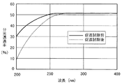
次に、以上の装置50又は80内から取り出した後に、接合面からはみ出した余分なフッ素樹脂フィルムを除去して紫外線領域用接合光学素子を得る。この紫外線領域用接合光学素子の分光透過率を測定し、その後、紫外線照射によるハーフミラーの耐久性検査を行う促進試験(紫外線波長248nm、出力2mW/cm2での連続照射を行う)に3ヶ月間投入後、再度、分光透過率測定した結果を図2に示す。
【0055】
図2の結果から明らかなように、波長270nm以下では、促進試験後が促進試験前よりも透過率が低いが、波長270nm〜400nmの範囲では紫外線領域の透過率が良好であり、接着剤層での吸収はほとんどなく、さらに、長期の紫外線照射によっても、その特性がほとんど劣化していないことがわかる。また、波長200nm〜270nmの範囲でも透過があるので使用可能である。また、促進試験後の光学素子には、接合面での剥離や接着剤層の亀裂は見いだせなかった。
【0056】
このような紫外線領域用接合光学素子の透過率特性は、紫外線顕微鏡の紫外線照明系のビームスプリッター等、紫外線領域で使用される際に必要とされる光学特性を満足し、また光源からの紫外線の照射によって発生する熱(前記促進試験時での発熱温度180℃)に耐える耐熱性を兼ね備えているため、同様の用途において十分使用できるものである。
【0057】
以上のように、この実施の形態の紫外線領域用接合光学素子によれば、紫外線領域(波長200nm〜400nm)で高い透過率を示し、接着剤層の硬化を短時間で行うことができ、接合状態での界面の剥離や接着剤層の亀裂がなく、さらには長期にわたって波長200nm以上の紫外線領域の透過率を維持することが可能となる。
【0058】
(実施の形態2)
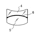
図3は実施の形態2の紫外線領域用接合光学素子を示し、石英レンズ4と蛍石レンズ5を有機フッ素樹脂からなる接着剤層6を介して接合することにより作製された貼り合わせレンズとなっている。
【0059】
この実施の形態で使用した有機フッ素樹脂は、含フッ素脂肪族エーテル環構造を主鎖に有したパーフルオロ(2,2−ジメチル−1,3−ジオキソール)の非晶質の重合物である。この有機フッ素樹脂をパーフルオロ(2−ブチルテトラヒドロフラン)またはパーフルオロベンゼン等のパーフルオロ化合物からなる溶剤中に、約10wt%溶解させた溶液を接着剤として用いる。なお、各レンズと接着剤層との密着性を高めるために、カップリング剤を1wt%前後混合しても良い。この溶液は、溶剤が完全に揮発したときには、炭素原子、フッ素原子、酸素原子および水素原子の4原子のみからなる有機フッ素樹脂層を形成するものである。
【0060】
この実施の形態の紫外線領域用接合光学素子を製造するには、まず石英レンズ4の接合面に、上述した有機フッ素樹脂溶液を滴下し、その上に蛍石レンズ5を載せて、加圧して気泡を除去しながら各接合面で樹脂溶液を延ばして接着剤層6を薄くする。又、石英レンズ4と蛍石レンズ5の光学芯を出して位置を合わせた後、治具でその位置を固定し、軽く加圧したまま、常温下で約6時間、接着剤層の溶剤が自然揮発により完全に抜けきるまで放置して、レンズ4,5が接合された紫外線領域用接合光学素子とする。このときの接着剤層6の厚さは5μmであった。また接合面からはみ出した余分な接着剤の固化物は除去した。
【0061】
この実施の形態の紫外線領域用接合光学素子を用いて、実施の形態1と同様に、紫外線照射の促進試験を実施して、試験前後の紫外線領域の分光透過率を測定した。図4は測定結果を示す。
【0062】
図4の結果から明らかなように、波長250nm以下では、促進試験後が促進試験前よりも透過率が幾分低いが、波長240nm〜400nmの範囲では、紫外線領域の透過率は90%以上で良好となっており、接着剤層6での吸収は極めて少なくなっている。又、長期の紫外線照射によっても、その特性がほとんど劣化していないことがわかる。さらに、促進試験後の光学素子には、接合面での剥離や接着剤層の亀裂は見いだせなかった。
【0063】
このような紫外線領域用接合光学素子の透過特性は、紫外線顕微鏡の対物レンズ系内の貼り合わせレンズや、エキシマレーザーを応用した様々な機器類の接合光学系やこれらと同様の用途において十分使用できるものである。
【0064】
この実施の形態の紫外線領域用接合光学素子によれば、紫外線領域で高い透過率を示し、接着剤層の硬化を行うのに際して加熱設備が不要な常温下で短時間で確実に可能であり、しかも接合状態で界面の剥離や接着剤層の亀裂がなく、さらに長期にわたって波長200nm以上の紫外線領域の透過率を維持することが可能となる。
【0065】
なお、実施の形態2では、接着剤層の溶剤を自然揮発により除去しているが、これに限らず加熱雰囲気下で溶剤の揮発を促進するようにしても良く、これにより作業性と接着力を高めることが可能となる。
【0066】
(実施の形態3)
この実施の形態の紫外線領域用接合光学素子は、実施の形態1における有機フッ素樹脂であるテトラフルオロエチレン−エチレン共重合体(ETFE)の6μm厚のフィルムに代えて、ポリフッ化ビニリデン(PVdF)の6μm厚のフィルムを接着剤層として用いた。そして、加熱温度を180℃、加熱時間を5分にした以外は実施の形態1と同様とした。このPVdFはその分子中に炭素原子、フッ素原子、酸素原子および水素原子の4原子のみを有し、融点が約130℃である。なお、貼り合わせプリズムの分光透過率と分光反射率は、設計上それぞれ55%、45%となるように設定されている。
【0067】
図5は、この実施の形態の紫外線領域用接合光学素子を、実施の形態1と同様の紫外線照射の促進試験を実施して、試験前後の紫外線領域の分光透過率を測定した結果を示す。図5から明らかなように、波長260nm以下では、促進試験後が促進試験前よりも透過率が低いが、波長260nm〜400nmの範囲では、紫外線領域の透過率は良好となっており、接着剤層での吸収は極めて少なくなっている。又、長期の紫外線照射によっても、その特性がほとんど劣化していないことがわかる。また、波長200nm〜260nmの範囲でも透過があるので使用可能である。さらに、促進試験後の光学素子には、接合面での剥離や接着剤層の亀裂は見いだせなかった。
【0068】
このように、この実施の形態によれば、紫外線領域(波長200nm〜400nm)で高い透過率を示し、接着剤層を容易に短時間で確実にでき、接合状態における界面の剥離や接着剤層の亀裂がなく、さらには長期にわたって波長200nm以上の紫外線領域の透過率を維持することが可能となる。
【0069】
(実施の形態4)
この実施の形態の紫外線領域用接合光学素子は、実施の形態2における含フッ素脂肪族エーテル環構造を主鎖に有したパーフルオロ(2,2ジメチル−1,3−ジオキソール)の非晶質の重合物からなる有機フッ素樹脂に代えて、ポリフッ化ビニリデン(PVdF)を有機フッ素樹脂として用いた。そして、このポリフッ化ビニリデン(PVdF)粉末をアセトン中に30wt%溶解させて溶液とした以外は、実施の形態2と同様とした。
【0070】
図6はこの実施の形態の紫外線領域用接合光学素子を、実施の形態1と同様の紫外線照射の促進試験を実施して、試験前後の紫外線領域の分光透過率を測定した結果を示す。図6から明らかなように、波長240nm以下では、促進試験後が促進試験前よりも透過率が幾分低いが、波長240nm〜400nmの範囲では、紫外線領域の透過率は90%以上で良好となっており、接着剤層での吸収は極めて少なくなっている。又、長期の紫外線照射によっても、その特性がほとんど劣化していないことがわかる。さらに、促進試験後の光学素子には、接合面での剥離や接着剤層の亀裂は見いだせなかった。
【0071】
従って、この実施の形態によれば、紫外線領域で高い透過率を示し、接着剤層の硬化を行うのに際して加熱設備の不要な常温下で短時間で確実にでき、接合状態で界面の剥離や接着剤層の亀裂がなく、さらには長期にわたって波長が200nm以上の紫外線領域の透過率を維持することが可能となる。
【0072】
なお、実施の形態では、接着剤層からアセトンを除去するため、自然揮発に限らず、加熱雰囲気下で溶剤の揮発を促進するようにしても良く、これにより作業性を高めることが可能となる。
【0073】
【発明の効果】
以上のように、請求項1によれば、紫外線領域で高い透過率を示し、接着剤の硬化を短時間で行うことができ、しかも接合状態で界面の剥離や接着剤層の亀裂がなく、長期にわたって紫外線領域の透過率を維持することが可能となる。
【0074】
請求項2の発明によれば、紫外線領域で高い透過率を示し、接着剤の硬化が短時間で終了し、しかも接合状態での界面の剥離や接着剤層の亀裂や光学歪の発生が極めて少なく、常温等の低温域下でも容易に接合でき、長期の高エネルギーの紫外線照射によっても紫外線領域の透過率が劣化し難い紫外線領域用接合光学素子とすることができる。
【0075】
請求項3の発明によれば、請求項1又は2の発明の効果に加えて、接着剤層中に気泡が残らない紫外線領域用接合光学素子とすることができる。
【0076】
請求項4の発明によれば、請求項1〜3の効果に加えて、接合層の厚さ調節が容易な紫外線領域用接合光学素子とすることができる。
【0077】
請求項5の発明によれば、請求項4の効果に加えて、紫外線領域用接合光学素子自体の分光透過率、分光反射率の設定が容易な紫外線領域用接合光学素子とすることができる。
【図面の簡単な説明】
【図1】実施の形態1及び3の紫外線領域用接合光学素子の側面図である。
【図2】実施の形態1の紫外線領域用接合光学素子の分光透過率の特性図である。
【図3】実施の形態2及び4の紫外線領域用接合光学素子の側面図である。
【図4】実施の形態2の紫外線領域用接合光学素子の分光透過率の特性図である。
【図5】実施の形態3の紫外線領域用接合光学素子の分光透過率の特性図である。
【図6】実施の形態4の紫外線領域用接合光学素子の分光透過率の特性図である。
【図7】光学素子を接合する装置の正面図である。
【図8】光学素子を接合する別の装置の正面図である。
【符号の説明】
1 2 石英プリズム
3 接着剤層[0001]
BACKGROUND OF THE INVENTION
The present invention relates to a cemented optical element used in a transmission optical system such as a cemented lens and a cemented prism, and more particularly to a cemented optical element for an ultraviolet region used in the ultraviolet region, such as an objective lens of an ultraviolet microscope.
[0002]
[Prior art]
A balsam, epoxy, or acrylate ultraviolet curable adhesive is used for bonding of the bonding optical elements used in the transmission optical system. This is because the conventional optical system was mainly used in the visible light region (wavelength of 400 nm or more), and thus the light transmittance of the adhesive used was intended only for the visible light region. .
[0003]
Recently, however, higher precision resolution is required in the field of optical technology. Therefore, a transmission optical system using ultraviolet rays having a short wavelength is desired. In view of this, as disclosed in JP-A-10-142498, an objective lens that makes extensive use of a bonded form of a quartz lens and a fluorite lens has been developed and proposed as a cemented lens for ultraviolet rays. However, since the adhesive used for bonding in the visible light region does not have a high light transmittance in the ultraviolet region (
[0004]
On the other hand, Japanese Patent No. 2786996 proposes a bonded optical element that can be used even in the ultraviolet region by using silicone alcoholate as an adhesive and hydrolyzing it to bond the optical elements. ing. Japanese Laid-Open Patent Publication No. 9-80207 proposes an optical lens for an ultraviolet irradiation apparatus in which a dielectric film is coated on a bonding interface of optical elements to be bonded and bonded with an ultraviolet curable adhesive.
[0005]
[Problems to be solved by the invention]
However, as disclosed in Japanese Patent No. 2786996, in a bonding optical element using silicone alcoholate, although ultraviolet rays are transmitted, the adhesive is hydrolyzed and cured, so that moisture is supplied to the bonding layer for curing. It is necessary. Further, when the lens or prism is joined, there is a problem that the supply of moisture is not sufficient and it takes a very long time (several days) to cure.
[0006]
Moreover, in this bonded optical element, since the curing form is due to a dehydration condensation reaction, curing shrinkage occurs during curing, peeling occurs at the interface between the optical element and the adhesive, or the adhesive layer is brittle and cracked, There is a problem that causes the occurrence of optical distortion.
[0007]
Furthermore, even if it initially has a high transmittance in the ultraviolet region, if it continues to transmit light in the ultraviolet region for a long time, the adhesive molecules will gradually cleave and depolymerize. It deteriorates and enters a state where it peels off or emits fluorescence. For this reason, the problem that initial performance cannot be maintained for a long time also arises.
[0008]
On the other hand, as disclosed in JP-A-9-80207, when a derivative film is coated on the bonding interface and bonded with an ultraviolet curable adhesive, not only a little effect is seen in a short wavelength region of a wavelength of 300 nm or less, The ultraviolet curable adhesive is also easily deteriorated by the ultraviolet rays in this region, and has a problem that it cannot withstand long-term use because it emits fluorescence.
[0009]
The present invention has been made in consideration of such conventional problems, and the object of the invention of claim 1 is to exhibit high transmittance in the ultraviolet region, and the curing of the adhesive is completed in a short time, In addition, there is very little occurrence of interfacial debonding, adhesive layer cracking and optical distortion in the bonded state, and long-termEven with high-energy UV irradiation, the transmittance in the UV region is unlikely to deteriorate.An object of the present invention is to provide a bonding optical element for ultraviolet region capable of maintaining the transmittance.
[0010]
The object of the invention of
[0011]
The object of the invention of
[0012]
The object of the invention of
[0013]
An object of the invention of
[0014]
[Means for Solving the Problems]
The invention according to claim 1 is a bonding optical element for ultraviolet region in which an optical element that transmits ultraviolet rays is bonded via an adhesive layer, wherein the adhesive layer does not have an unsaturated bond in the molecule.It has only 4 atoms of carbon atom, fluorine atom, oxygen atom and hydrogen atomIt consists of an organic fluororesin.
[0015]
The organic fluororesin used in the present invention does not have an unsaturated bond in the molecule. The carbon-fluorine bond of the organic fluororesin has a bond energy of 107 kcal / mol, a carbon-carbon bond energy of 83.1 kcal / mol, a carbon-hydrogen bond energy of 98.8 kcal / mol, and a carbon-oxygen. The bond energy is 84.0 kcal / mol between the carbon atoms, the bond energy between carbon and nitrogen is 69.7 kcal / mol, the bond energy between carbon and chlorine is 78.5 kcal / mol, and the bond is very strong. In addition, the carbon-carbon bond energy linked to carbon-fluorine is reinforced by fluorine, and the resin is stable electrically, chemically and thermally.
[0016]
In addition, since the organic fluororesin is a resin material with high heat resistance and forms a relatively flexible film, even if stress is generated, the stress can be absorbed by the flexibility of the adhesive layer, and optical distortion is reduced. be able to.
[0017]
However, the organic fluororesin may have a functional group such as a vinyl group or an acryloyl group in order to have reactivity with other materials, or a phenyl group in order to provide solubility in a solvent, Some of them have a carbonyl group, carboxyl group, cyano group, triazine ring structure, etc. The structure having such an unsaturated bond is excited by ultraviolet rays to cause depolymerization or the like, and easily emits fluorescence. This is unsuitable for bonding optical elements. Therefore, in the present invention, an organic fluororesin having a structure having an unsaturated bond is not used.
[0018]
Examples of the organic fluororesin having no unsaturated bond in the molecule include polytetrafluoroethylene (PTFE), tetrafluoroethylene-perfluoroalkyl vinyl ether copolymer (PFA), and tetrafluoroethylene-hexafluoropropylene copolymer (FEP). ), Tetrafluoroethylene-ethylene copolymer (ETFE), polychlorotrifluoroethylene (PCTFE), polyvinyl fluoride (PVF), polyvinylidene fluoride (PVdF), and other resins having a fluorine-containing ring structure. is there. Some grades are made higher by removing impurities (such as dust and ionic impurities) from these fluororesins having no unsaturated bond. These have high transparency up to the ultraviolet region, are hardly deteriorated by long-term ultraviolet irradiation, and have stable optical characteristics. Of these, those having a relatively low molecular weight are more easily obtained.
[0019]
Therefore, even when such an organic fluororesin having no unsaturated bond is used as a bonding layer between optical elements for the ultraviolet region, it may be excited by ultraviolet rays to cause depolymerization or emit fluorescence. Therefore, it is possible to provide a bonded optical element for an ultraviolet region that has transparency up to the ultraviolet region and does not deteriorate even when irradiated for a long time.
In addition, since the organic fluororesin used in the present invention has a structure having only four atoms of carbon atom, fluorine atom, oxygen atom and hydrogen atom in addition to having an unsaturated bond in the molecule, The state is firmly stabilized, and even when high energy of ultraviolet rays is irradiated over a long period of time, the bonded state can be maintained satisfactorily without being mechanically or optically degraded.
[0020]
In addition, such a bonding optical element is a process of wetting without introducing defects such as bubbles on the entire surface of the optical element for bonding the organic fluororesin as a bonding layer, while the bonding layer is fluidized, The process of positioning (centering) optical elements to be bonded while controlling the thickness of the bonding layer, the process of solidifying the bonding layer while positioning the optical elements to be bonded, and removing the excess bonding layer It is produced by the process of. In addition, in order to efficiently perform these processes, the optical element is bonded by using a bonding device that controls the bonding layer thickness, a jig for positioning, a device that solidifies the bonding layer while positioning, and the like. Let
[0021]
The invention of claim 2In a bonding optical element for an ultraviolet region in which an optical element that transmits ultraviolet light is bonded via an adhesive layer, the adhesive layer has no fluorine-containing aliphatic ether ring structure in the main chain and has no unsaturated bond in the molecule. Made of organic fluororesinIt is characterized by that.
[0022]
The organic fluororesin used in the present invention isAs in the first aspect of the invention, the adhesive layer has a structure having no unsaturated bond in the molecule and having a fluorine-containing aliphatic ether ring structure in the main chain. This organic fluororesin is easily dissolved in a specific solvent such as a perfluoro compound solvent such as perfluorobenzene, perfluoro (2-butyltetrahydrofuran), and perfluorotributylamine. Wetting can be performed without introducing defects such as bubbles, and uniform film thickness control can be facilitated to reduce variation in transmittance. Further, since it is amorphous, the transmittance in the ultraviolet region is excellent, the bonding state of the whole molecule is firmly stabilized, and the bonding state can be maintained well even when high energy of ultraviolet rays is irradiated for a long period of time.
[0023]
Such a bonded optical element is,ContactControl the thickness of the bonding layer while the bonding layer is fluidized by heating and melting the organic fluororesin used as the bonding layer to wet the entire surface between the optical elements to be bonded without introducing defects such as bubbles. The step of positioning (centering) the optical elements to be bonded together, the step of gradually cooling and solidifying the bonding layer in the state where the optical elements to be bonded are positioned, and removing the excess bonding layer It is produced by a process. Further, in order to efficiently perform these steps, an apparatus for bonding while controlling the bonding layer thickness, a jig for positioning, an apparatus for solidifying the bonding layer while positioning, and the like are used. In particular, in the step of solidification by heating and slow cooling, jigs and devices that prevent misalignment between optical elements are used.
[0024]
The invention of
[0025]
The organic fluororesin used in the present invention is a solvent-soluble type. A solution obtained by dissolving the solvent-soluble organic fluororesin with a solvent is likely to wet the surface of the optical element. The organic fluororesin solution is supplied between the optical elements to wet the entire surface of the optical element, and then the solvent is volatilized from the fluororesin solution. Thereby, the fluororesin interposed between the optical elements is solidified, and the optical elements are bonded to each other to obtain a bonded optical element.
[0026]
Such a bonded optical element is,ContactThe step of dissolving the organic fluororesin used as a layer in a solvent, the step of wetting and spreading without introducing defects such as bubbles throughout the surfaces of the optical elements to be bonded, and the bonding layer thickness while the bonding layer is fluidized The process of positioning the optical elements to be bonded while controlling the position, the process of volatilizing and removing the solvent from the bonding layer while positioning the optical elements to be bonded, removing the excess bonding layer It is produced by the process to do. Further, in order to efficiently perform these steps, an apparatus for bonding while controlling the bonding layer thickness, an apparatus for preventing misalignment in the solvent volatilization process, cracking of the bonding layer, and mixing of bubbles are used.
[0027]
Invention of
[0028]
In this inventionSince the organic fluororesin is in the form of a film, the thickness of the bonding layer can be easily adjusted.
[0029]
The invention of
[0030]
In this inventionIs a coating on the bonding surface of one optical element and then bonding through the film-like organic fluororesin, so setting of the spectral transmittance and spectral reflectance of the bonding optical element itself for the ultraviolet region Becomes easy.
[0031]
DETAILED DESCRIPTION OF THE INVENTION
(Embodiment 1)
The cemented optical element for ultraviolet region of this embodiment is composed of a bonded prism as shown in FIG. In this prism, a quartz prism 1 having a high ultraviolet transmittance and a
[0032]
As the organic fluororesin of the
[0033]
In order to manufacture the bonded optical element for the ultraviolet region of this embodiment, first, the ETFE film is used as an organic fluororesin film having high transparency from the visible light region to the ultraviolet region (
[0034]
When laminating in the apparatus, the heating condition is 310 ° C. for 5 minutes, and the pressing condition is about 5 kg / cm.2And While gradually declining, the pressure is released when the temperature drops to about 100 ° C., and the temperature is further cooled to room temperature in the apparatus.
[0035]
FIG. 7 shows an apparatus used for bonding. This
[0036]
A V-shaped
[0037]
A
[0038]
A
[0039]
A
[0040]
Below the
[0041]
When a bonded prism is manufactured using this
[0042]
Then, with the
[0043]
A case where the thickness of the film (bonding layer) is adjusted during the bonding will be described. In the case of reducing the thickness of the film, the
[0044]
When the film thickness is increased, the
[0045]
In order to reduce the film thickness, the
[0046]
After positioning the two
[0047]
FIG. 8 shows another
[0048]
The
[0049]
In addition,
[0050]
In order to manufacture a bonded prism using the
[0051]
The position of each joint surface is detected by the first
[0052]
When the detection signals from the first
[0053]
In such an
[0054]
Next, after taking out from the
[0055]
As apparent from the results of FIG. 2, the transmittance after the accelerated test is lower than that before the accelerated test at a wavelength of 270 nm or less, but the transmittance in the ultraviolet region is good in the wavelength range of 270 nm to 400 nm, and the adhesive layer It can be seen that there is almost no absorption in the film, and that the characteristics are hardly deteriorated by long-term ultraviolet irradiation. Further, since there is transmission even in the wavelength range of 200 nm to 270 nm, it can be used. Further, in the optical element after the acceleration test, no peeling at the joint surface or cracking of the adhesive layer was found.
[0056]
The transmittance characteristics of such a bonded optical element for the ultraviolet region satisfy the optical properties required when used in the ultraviolet region, such as a beam splitter of an ultraviolet illumination system of an ultraviolet microscope, and also the ultraviolet light from the light source. Since it has heat resistance that can withstand the heat generated by irradiation (the heat generation temperature of 180 ° C. during the accelerated test), it can be sufficiently used in similar applications.
[0057]
As described above, according to the bonding optical element for the ultraviolet region of this embodiment, it exhibits high transmittance in the ultraviolet region (wavelength of 200 nm to 400 nm), and the adhesive layer can be cured in a short time. There is no peeling of the interface or cracking of the adhesive layer in the state, and it is possible to maintain the transmittance in the ultraviolet region having a wavelength of 200 nm or more for a long time.
[0058]
(Embodiment 2)
FIG. 3 shows a cemented optical element for an ultraviolet region according to the second embodiment, which is a bonded lens manufactured by bonding a
[0059]
The organic fluororesin used in this embodiment is an amorphous polymer of perfluoro (2,2-dimethyl-1,3-dioxole) having a fluorine-containing aliphatic ether ring structure in the main chain. A solution prepared by dissolving about 10 wt% of this organic fluororesin in a solvent composed of a perfluoro compound such as perfluoro (2-butyltetrahydrofuran) or perfluorobenzene is used as an adhesive. In order to improve the adhesion between each lens and the adhesive layer, a coupling agent may be mixed around 1 wt%. When the solvent is completely volatilized, this solution forms an organic fluororesin layer consisting of only four atoms of carbon atoms, fluorine atoms, oxygen atoms and hydrogen atoms.
[0060]
In order to manufacture the cemented optical element for the ultraviolet region of this embodiment, first, the above-mentioned organic fluororesin solution is dropped on the cemented surface of the
[0061]
Using the ultraviolet optical bonding optical element of this embodiment, an ultraviolet irradiation acceleration test was conducted in the same manner as in Embodiment 1 to measure the spectral transmittance in the ultraviolet region before and after the test. FIG. 4 shows the measurement results.
[0062]
As is clear from the results of FIG. 4, the transmittance after the accelerated test is somewhat lower than that before the accelerated test at a wavelength of 250 nm or less, but in the wavelength range of 240 nm to 400 nm, the transmittance in the ultraviolet region is 90% or higher. It is good and the absorption in the
[0063]
The transmission characteristics of such a bonding optical element for the ultraviolet region can be sufficiently used in a bonding lens in an objective lens system of an ultraviolet microscope, a bonding optical system of various devices to which excimer laser is applied, and similar applications. Is.
[0064]
According to the bonding optical element for the ultraviolet region of this embodiment, it exhibits high transmittance in the ultraviolet region, and can be reliably performed in a short time at room temperature that does not require heating equipment when curing the adhesive layer. In addition, there is no peeling of the interface or cracking of the adhesive layer in the bonded state, and the transmittance in the ultraviolet region having a wavelength of 200 nm or more can be maintained for a long period of time.
[0065]
In the second embodiment, the solvent of the adhesive layer is removed by natural volatilization. However, the present invention is not limited to this, and the volatilization of the solvent may be promoted in a heated atmosphere. Can be increased.
[0066]
(Embodiment 3)
The bonding optical element for ultraviolet region of this embodiment is made of polyvinylidene fluoride (PVdF) instead of a 6 μm thick film of tetrafluoroethylene-ethylene copolymer (ETFE) which is an organic fluororesin in the first embodiment. A 6 μm thick film was used as the adhesive layer. And it was the same as that of Embodiment 1 except having made heating temperature into 180 degreeC and heating time into 5 minutes. This PVdF has only 4 atoms of carbon atom, fluorine atom, oxygen atom and hydrogen atom in its molecule, and its melting point is about 130 ° C. The spectral transmittance and spectral reflectance of the bonded prism are set to 55% and 45%, respectively, in design.
[0067]
FIG. 5 shows the result of measuring the spectral transmittance in the ultraviolet region before and after the test by carrying out the same ultraviolet irradiation acceleration test as in the first embodiment on the bonded optical element for the ultraviolet region in this embodiment. As is apparent from FIG. 5, the transmittance after the accelerated test is lower than that before the accelerated test at a wavelength of 260 nm or less, but the transmittance in the ultraviolet region is good in the wavelength range of 260 nm to 400 nm. The absorption in the layer is very low. It can also be seen that the characteristics are hardly deteriorated even by long-term ultraviolet irradiation. Further, since there is transmission even in the wavelength range of 200 nm to 260 nm, it can be used. Furthermore, no peeling at the joint surface or cracks in the adhesive layer were found in the optical element after the acceleration test.
[0068]
As described above, according to this embodiment, high transmittance is exhibited in the ultraviolet region (
[0069]
(Embodiment 4)
The bonding optical element for the ultraviolet region of this embodiment is an amorphous perfluoro (2,2dimethyl-1,3-dioxole) having the fluorine-containing aliphatic ether ring structure in the main chain in the second embodiment. Instead of the organic fluororesin made of a polymer, polyvinylidene fluoride (PVdF) was used as the organic fluororesin. Then, the same procedure as in
[0070]
FIG. 6 shows the result of measuring the spectral transmittance in the ultraviolet region before and after the test by carrying out the same ultraviolet irradiation acceleration test as in Embodiment 1 on the bonded optical element for the ultraviolet region in this embodiment. As is apparent from FIG. 6, the transmittance after the accelerated test is somewhat lower than that before the accelerated test at a wavelength of 240 nm or less, but the transmittance in the ultraviolet region is 90% or more and good at a wavelength of 240 nm to 400 nm. The absorption in the adhesive layer is extremely low. It can also be seen that the characteristics are hardly deteriorated even by long-term ultraviolet irradiation. Furthermore, no peeling at the joint surface or cracks in the adhesive layer were found in the optical element after the acceleration test.
[0071]
Therefore, according to this embodiment, it exhibits high transmittance in the ultraviolet region, and can be reliably performed in a short time at an ordinary temperature that does not require any heating equipment when curing the adhesive layer. There is no crack in the adhesive layer, and furthermore, it is possible to maintain the transmittance in the ultraviolet region having a wavelength of 200 nm or longer over a long period of time.
[0072]
In the embodiment, since acetone is removed from the adhesive layer, the volatilization of the solvent may be promoted not only in the natural volatilization but also in a heating atmosphere, thereby improving the workability. .
[0073]
【The invention's effect】
As described above, according to the first aspect of the present invention, high transmittance is exhibited in the ultraviolet region, the adhesive can be cured in a short time, and there is no peeling of the interface or cracking of the adhesive layer in the bonded state. It becomes possible to maintain the transmittance in the ultraviolet region over a long period of time.
[0074]
According to the invention of
[0075]
According to the invention of
[0076]
According to the invention of
[0077]
According to the invention of
[Brief description of the drawings]
FIG. 1 is a side view of a bonding optical element for an ultraviolet region according to
FIG. 2 is a characteristic diagram of spectral transmittance of the bonding optical element for ultraviolet region according to the first embodiment.
FIG. 3 is a side view of an ultraviolet region cemented optical element according to
FIG. 4 is a characteristic diagram of spectral transmittance of the bonding optical element for ultraviolet region according to the second embodiment.
FIG. 5 is a characteristic diagram of spectral transmittance of the bonding optical element for ultraviolet region according to the third embodiment.
FIG. 6 is a characteristic diagram of spectral transmittance of the bonding optical element for ultraviolet region according to the fourth embodiment.
FIG. 7 is a front view of an apparatus for joining optical elements.
FIG. 8 is a front view of another apparatus for joining optical elements.
[Explanation of symbols]
1 2 Quartz prism
3 Adhesive layer
Claims (5)
前記接着剤層が分子内に不飽和結合を有しない、炭素原子とフッ素原子と酸素原子と水素原子の4原子のみを有する有機フッ素樹脂からなることを特徴とする紫外線領域用接合光学素子。In a bonding optical element for ultraviolet region in which an optical element that transmits ultraviolet light is bonded via an adhesive layer,
A bonding optical element for an ultraviolet region, wherein the adhesive layer is made of an organic fluororesin having no unsaturated bond in the molecule and having only four atoms of carbon atom, fluorine atom, oxygen atom and hydrogen atom.
前記接着剤層が分子内に不飽和結合を有しない、含フッ素脂肪族エーテル環構造を主鎖に有する有機フッ素樹脂からなることを特徴とする紫外線領域用接合光学素子。In a bonding optical element for ultraviolet region in which an optical element that transmits ultraviolet light is bonded via an adhesive layer,
A bonding optical element for an ultraviolet region, wherein the adhesive layer is made of an organic fluororesin having a fluorine-containing aliphatic ether ring structure in the main chain and having no unsaturated bond in the molecule.
Priority Applications (1)
| Application Number | Priority Date | Filing Date | Title |
|---|---|---|---|
| JP2000099237A JP4663060B2 (en) | 2000-03-31 | 2000-03-31 | Bonding optical element for ultraviolet region |
Applications Claiming Priority (1)
| Application Number | Priority Date | Filing Date | Title |
|---|---|---|---|
| JP2000099237A JP4663060B2 (en) | 2000-03-31 | 2000-03-31 | Bonding optical element for ultraviolet region |
Publications (2)
| Publication Number | Publication Date |
|---|---|
| JP2001281551A JP2001281551A (en) | 2001-10-10 |
| JP4663060B2 true JP4663060B2 (en) | 2011-03-30 |
Family
ID=18613614
Family Applications (1)
| Application Number | Title | Priority Date | Filing Date |
|---|---|---|---|
| JP2000099237A Expired - Fee Related JP4663060B2 (en) | 2000-03-31 | 2000-03-31 | Bonding optical element for ultraviolet region |
Country Status (1)
| Country | Link |
|---|---|
| JP (1) | JP4663060B2 (en) |
Families Citing this family (7)
| Publication number | Priority date | Publication date | Assignee | Title |
|---|---|---|---|---|
| JP2006267530A (en) * | 2005-03-24 | 2006-10-05 | Mitsubishi Electric Corp | Illumination device and projection display device |
| WO2008136243A1 (en) * | 2007-04-27 | 2008-11-13 | Konica Minolta Opto, Inc. | Manufacturing method and jointing jig for optical element |
| US20110149589A1 (en) * | 2008-07-30 | 2011-06-23 | Ams Research Corporation | Optical device having fluorocarbon polymer layer |
| JP5608402B2 (en) * | 2010-03-30 | 2014-10-15 | オリンパス株式会社 | Method for manufacturing composite optical element and apparatus for manufacturing the same |
| US8672929B2 (en) | 2010-12-15 | 2014-03-18 | Ams Research Corporation | Laser probe tip |
| JP2017018483A (en) * | 2015-07-14 | 2017-01-26 | オリンパス株式会社 | Medical probe |
| JP7683283B2 (en) * | 2021-03-31 | 2025-05-27 | セイコーエプソン株式会社 | Optical element, projection optical device, and projector |
Family Cites Families (2)
| Publication number | Priority date | Publication date | Assignee | Title |
|---|---|---|---|---|
| US5349004A (en) * | 1992-09-18 | 1994-09-20 | Minnesota Mining And Manufacturing Company | Fluoroalkyl siloxane/vinyl copolymer dispersions and pressure-sensitive adhesives having improved solvent resistance prepared therefrom |
| JP3258408B2 (en) * | 1992-12-29 | 2002-02-18 | オリンパス光学工業株式会社 | Optical element holding device |
-
2000
- 2000-03-31 JP JP2000099237A patent/JP4663060B2/en not_active Expired - Fee Related
Also Published As
| Publication number | Publication date |
|---|---|
| JP2001281551A (en) | 2001-10-10 |
Similar Documents
| Publication | Publication Date | Title |
|---|---|---|
| JP4663060B2 (en) | Bonding optical element for ultraviolet region | |
| CN102012335B (en) | Retainer, performance test apparatus and performance test method | |
| US20150101743A1 (en) | Methods and Materials for Fabricating Laminate Nanomolds and Nanoparticles Therefrom | |
| US20090017248A1 (en) | Layered body and method for manufacturing thin substrate using the layered body | |
| EP2927746B1 (en) | A pellicle for lithography | |
| KR101326497B1 (en) | Method of molding | |
| CN1480724A (en) | Bonding and packaging method and device for plastic biochip | |
| JP2012071555A (en) | Method and apparatus for producing lens, lens produced by the method, and lens unit comprising the lens | |
| TW201835120A (en) | Fluoropolymer, method for producing cured product thereof, and light-emitting device | |
| Uddin et al. | Adhesive technology for photonics | |
| TWI388587B (en) | A method for producing a hardened resin molded body, and a hardened resin molded product | |
| KR20220059170A (en) | Compound for adhesive, method for fabricating the same, reticle assembly including the same, and method for fabricating reticle assembly including the same | |
| JP5657296B2 (en) | Composite optical element alignment method and alignment apparatus therefor | |
| EP1835315A1 (en) | Waveguide forming methods and waveguides fabricated therefrom | |
| JP2843672B2 (en) | Pellicle film having antireflection layer | |
| JP3944615B2 (en) | Laser-assisted processing equipment | |
| JPH01163201A (en) | Production of molded article of transparent plastic | |
| JP5514630B2 (en) | Lens manufacturing apparatus, lens manufacturing method, lens, and imaging apparatus | |
| JP2002251802A (en) | Method of manufacturing disk-shaped recording medium and mold apparatus | |
| TWI854305B (en) | Enhanced thermal release adhesive material, structure thereof and manufacturing method thereof | |
| JP2009233855A (en) | Transfer mold, method for manufacturing transfer mold, and method for manufacturing transferred product using the transfer mold | |
| US20230303853A1 (en) | Continuous three-dimensional printing of architected piezoelectric sensors | |
| JP5608402B2 (en) | Method for manufacturing composite optical element and apparatus for manufacturing the same | |
| CN1200809C (en) | Compound lens manufacturing device and compound lens manufacturing method | |
| JP2011245637A (en) | Lens mold, lens manufacturing apparatus, lens manufactured by lens manufacturing apparatus, and imaging device equipped with lens |
Legal Events
| Date | Code | Title | Description |
|---|---|---|---|
| A621 | Written request for application examination |
Free format text: JAPANESE INTERMEDIATE CODE: A621 Effective date: 20070402 |
|
| A131 | Notification of reasons for refusal |
Free format text: JAPANESE INTERMEDIATE CODE: A131 Effective date: 20100531 |
|
| A521 | Request for written amendment filed |
Free format text: JAPANESE INTERMEDIATE CODE: A523 Effective date: 20100723 |
|
| A131 | Notification of reasons for refusal |
Free format text: JAPANESE INTERMEDIATE CODE: A131 Effective date: 20100903 |
|
| A521 | Request for written amendment filed |
Free format text: JAPANESE INTERMEDIATE CODE: A523 Effective date: 20101013 |
|
| TRDD | Decision of grant or rejection written | ||
| A01 | Written decision to grant a patent or to grant a registration (utility model) |
Free format text: JAPANESE INTERMEDIATE CODE: A01 Effective date: 20101210 |
|
| A01 | Written decision to grant a patent or to grant a registration (utility model) |
Free format text: JAPANESE INTERMEDIATE CODE: A01 |
|
| A61 | First payment of annual fees (during grant procedure) |
Free format text: JAPANESE INTERMEDIATE CODE: A61 Effective date: 20110105 |
|
| FPAY | Renewal fee payment (event date is renewal date of database) |
Free format text: PAYMENT UNTIL: 20140114 Year of fee payment: 3 |
|
| S531 | Written request for registration of change of domicile |
Free format text: JAPANESE INTERMEDIATE CODE: R313531 |
|
| R350 | Written notification of registration of transfer |
Free format text: JAPANESE INTERMEDIATE CODE: R350 |
|
| LAPS | Cancellation because of no payment of annual fees |