JP4660731B2 - Regenerative repeater using bistable semiconductor laser - Google Patents
Regenerative repeater using bistable semiconductor laser Download PDFInfo
- Publication number
- JP4660731B2 JP4660731B2 JP2001244302A JP2001244302A JP4660731B2 JP 4660731 B2 JP4660731 B2 JP 4660731B2 JP 2001244302 A JP2001244302 A JP 2001244302A JP 2001244302 A JP2001244302 A JP 2001244302A JP 4660731 B2 JP4660731 B2 JP 4660731B2
- Authority
- JP
- Japan
- Prior art keywords
- light
- beam splitter
- clock
- semiconductor laser
- signal light
- Prior art date
- Legal status (The legal status is an assumption and is not a legal conclusion. Google has not performed a legal analysis and makes no representation as to the accuracy of the status listed.)
- Expired - Fee Related
Links
Images


Landscapes
- Semiconductor Lasers (AREA)
- Optical Communication System (AREA)
Description
【0001】
【発明の属する技術分野】
本発明は、双安定半導体レーザを用いた再生中継器に関するものである。
【0002】
【従来の技術】
現在、光ファイバ通信システムは高度情報化社会を担う通信伝送方式として発展している。しかし、現状の光ファイバ通信システムは、キャリア周波数が200THzという光の特性をまだ十分には活用していない。今後の情報量の増大に応えるためには、より一層の超高速光通信システムの開発が望まれているが、その超高速化のためには、信号処理も光が行う全光化が期待されている。
【0003】
【発明が解決しようとする課題】
従来、光ファイバ中で減衰した光信号は、光電変換して電子回路により、等化増幅(reshaping)、識別再生(regenerating)、リタイミング(retiming)を行い(これを3R機能という)、再び光信号に変換して光ファイバ中に送り出す、という再生中継が行われている。そのような再生中継方式においては、波形劣化と雑音の累積を回避できるという利点がある反面、複雑な回路構成となり、また、高速化が困難であるという問題があった。
【0004】
本発明は、上記状況に鑑みて、光信号を電気信号に変換することなく、全光型で直接再生中継を行い、簡単な構成で高速化を達成することができる双安定半導体レーザを用いた再生中継器を提供することを目的とする。
【0005】
【課題を解決するための手段】
本発明の特徴は、光信号を電気信号に変換することなく、全光型で直接再生中継を行うことにある。外部共振器型半導体レーザからなるクロック抽出回路と、双安定面発光半導体レーザのもつ、ANDゲート動作およびメモリ動作を組み合わせることにより可能となる。以下、構成例で説明する。
本発明は、上記目的を達成するために、
〔1〕双安定半導体レーザを用いた再生中継器において、入力信号光(1)を受ける第1のビームスプリッタ(2)と、この第1のビームスプリッタ(2)で2分割された一方の入力信号光(1)が入力されるとともに、片面にARコーティング(5A)を施した半導体レーザ(5)と前記ARコーティング(5A)と対向させて配置した鏡(6)とにより構成される外部共振器(7)よりなり、前記入力信号光(1)のパルスの時間間隔t 0 と等しい時間間隔のクロック光を抽出する第1のクロック抽出部(12)と、この第1のクロック抽出部(12)から得たクロック光を前記第1のビームスプリッタ(2)を介して受け、このクロック光を2分割する第2のビームスプリッタ(10)と、この第2のビームスプリッタ(10)で2分割された一方のクロック光をt 0 /4遅延させる光遅延器(13)と、この光遅延器(13)からのクロック光の偏光を90°回転するλ/2波長板(14)と、偏光方向が互いに等しい前記第1のビームスプリッタ(2)で2分割された他方の入力信号光(1)と前記第2のビームスプリッタ(10)で2分割された他方のクロック光とのAND動作で0°モードの出力信号光を出力するとともに、前記λ/2波長板(14)から出力される偏光方向が90°回転されたクロック光が入射され90°モードの出力信号光を出力する光導波路が正方形の断面形状を持つ面発光半導体レーザ(4)と、この面発光半導体レーザ(4)からの前記0°モードの出力信号光と前記90°モードの出力信号光とを分離する偏光ビームスプリッタ(18)とを備え、全光型で直接再生中継を行うことを特徴とする。
【0007】
【発明の実施の形態】
以下、本発明の実施の形態について詳細に説明する。
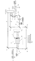
図1は本発明の実施例を示す双安定半導体レーザを用いた再生中継器の全体構成図、図2は面発光半導体レーザ(VCSEL)の機能の説明図である。
これらの図において、1は入力信号光、2は第1のビームスプリッタ、3は第1の反射鏡、4は面発光半導体レーザ(VCSEL)、5は半導体レーザであり、その片面にARコーティング5Aが施されている。6は鏡(M)であり、半導体レーザ5と合わせて外部共振器7を形成する。
【0008】
また、8は第2の反射鏡、9は第3の反射鏡、10は第2のビームスプリッタ、11は第4の反射鏡、12はクロック抽出回路、13はt0 /4の時間遅れを生成する光遅延器、14はλ/2波長板、15は第5の反射鏡、16は第3のビームスプリッタ、17は第4のビームスプリッタ、18は出力信号光(0°)と出力信号光(90°)とを生成する偏光ビームスプリッタ(PBS)である。
【0009】
まず、クロック抽出回路の構成例について説明する。
半導体レーザ5の片面にARコーティング5Aを施し、鏡(M)6と合わせて外部共振器7を形成する。入力信号光1のパルス間隔がt0 の場合、2L/c=t0 (Lは共振器長)の関係があれば、半導体レーザ5に注入されたパルスは、共振器内を周回し、RZ信号パルス列はパルス列に変換され、クロック抽出回路12として動作する。
【0010】
この時、抽出したクロックの波高値やパルスの時間位置の正確さは、半導体レーザ5の共振器反射率Rに大きく依存し、Rが1に近い方が良好なクロック抽出が可能となる。さらに、良好なパルス列を形成するため、半導体レーザ5内に可飽和吸収体を挿入したり、波長板と組み合わせることも可能である。
次に、再生中継器の構成例について説明する。
【0011】
クロック抽出回路12で入力信号からクロックを抽出した後、クロック信号を第2のビームスプリッタ10で2分割し、一方を光遅延器13でt0 /4だけ遅らせ、λ/2波長板14で信号の偏光を90°回転する。入力信号光1と2つのクロック光を双安定VCSEL4に入射する。0°入力信号光と0°クロック光のAND動作でVCSEL4が0°にセットされ、90°クロック光でVCSEL4は90°信号になる。これにより再生中継が可能になる。
【0012】
ここで、偏光双安定面発光半導体レーザについて説明する。
図3は本発明にかかる面発光半導体レーザ(VCSEL)の模式図、図4はこの面発光半導体レーザによる偏光双安定光メモリの動作の説明図であり、図4(a)は外部からの入射光(例えば、フェムト秒光パルス)の波形図、図4(b)は出力光のパルスの波形図である。
【0013】
これらの図に示すように、光導波路が正方形の断面形状を持つ、面発光半導体レーザ(VCSEL)4には、電界方向が正方形の辺に沿う2つの固有モードが存在する。ここでは0°モード、90°モードと呼ぶ。2つのレーザ発振モードに対して面発光半導体レーザの光学利得はほぼ等しく、2つのモードは利得飽和を通して強結合し、双安定性が生じる。
【0014】
光パルス(例えば、フェムト秒光パルス)を外部から入射すると、入射パルス光と同一偏光のモードに偏光がスイッチし、入射パルスがなくなってもスイッチした後の偏光を保持する。従って、偏光双安定光メモリが実現できる。偏光スイッチングの速度は7psと極めて速く、光双安定素子のスイッチング速度としては世界最高速である。そのため、超高速光通信における種々の超高速光機能素子として応用が期待できる。
【0015】
次に、光3R機能について説明する。
図5は本発明にかかる光3R機能の説明図である。
光3R機能では波形がなまり、時間位置にもジッターを含む光入力信号〔図5(a)参照〕から、システムで決められている周波数と一致したクロック信号を抽出し、このクロック信号を基準に、増幅と符号化とを行った信号を新しく送出する。
【0016】
その結果、図5(b)に示すように、時間ジッターがなく、波形および波高値ともにそろい、符号化された信号が再生される。
なお、上記実施例では、クロック抽出回路を半導体レーザと外部共振器の組み合わせとし例示したが、これに限定されるものではなく、他の構成をとるようにしてもよい。
【0017】
また、本発明は上記実施例に限定されるものではなく、本発明の趣旨に基づいて種々の変形が可能であり、これらを本発明の範囲から排除するものではない。
【0018】
【発明の効果】
以上、詳細に説明したように、本発明によれば、光信号を電気信号に変換することなく、全光型で直接再生中継を行い、簡単な構成と高速化を達成することができる。
【図面の簡単な説明】
【図1】 本発明の実施例を示す双安定半導体レーザを用いた再生中継器の全体構成図である。
【図2】 本発明にかかる面発光半導体レーザ(VCSEL)の機能の説明図である。
【図3】 本発明にかかる面発光半導体レーザ(VCSEL)の模式図である。
【図4】 本発明にかかる面発光半導体レーザによる偏光双安定光メモリの動作の説明図である。
【図5】 本発明にかかる光3R機能の説明図である。
【符号の説明】
1 入力信号光
2 第1のビームスプリッタ
3 第1の反射鏡
4 面発光半導体レーザ(VCSEL)
5 半導体レーザ
5A ARコーティング
6 鏡(M)
7 外部共振器
8 第2の反射鏡
9 第3の反射鏡
10 第2のビームスプリッタ
11 第4の反射鏡
12 クロック抽出回路
13 t0 /4の時間遅れを生成する光遅延器
14 λ/2波長板
15 第5の反射鏡
16 第3のビームスプリッタ
17 第4のビームスプリッタ
18 偏光ビームスプリッタ(PBS)[0001]
BACKGROUND OF THE INVENTION
The present invention relates to a regenerative repeater using a bistable semiconductor laser.
[0002]
[Prior art]
At present, the optical fiber communication system has been developed as a communication transmission system that bears an advanced information society. However, current optical fiber communication systems have not yet fully utilized the light characteristic of a carrier frequency of 200 THz. In order to respond to the increase in information volume in the future, further development of ultra-high-speed optical communication systems is desired, but for ultra-high speed, signal processing is expected to be all-optical. ing.
[0003]
[Problems to be solved by the invention]
Conventionally, an optical signal attenuated in an optical fiber is photoelectrically converted, subjected to equalization amplification (reshaping), identification regeneration (regeneration), and retiming (retiming) by an electronic circuit (this is called a 3R function), and the optical signal is again transmitted. Regenerative relaying is performed in which signals are converted and sent into optical fibers. Such a regenerative relay system has the advantage that waveform degradation and noise accumulation can be avoided, but has a problem that it has a complicated circuit configuration and is difficult to increase in speed.
[0004]
In view of the above situation, the present invention uses a bistable semiconductor laser capable of performing all-optical direct reproduction relay without converting an optical signal into an electrical signal and achieving high speed with a simple configuration. An object is to provide a regenerative repeater.
[0005]
[Means for Solving the Problems]
A feature of the present invention resides in that all-optical direct regenerative relaying is performed without converting an optical signal into an electrical signal. This can be achieved by combining the clock extraction circuit composed of an external resonator type semiconductor laser and the AND gate operation and memory operation of the bistable surface emitting semiconductor laser. Hereinafter, a configuration example will be described.
In order to achieve the above object, the present invention provides
[1] In a regenerative repeater using a bistable semiconductor laser, a first beam splitter (2) that receives an input signal light (1) and one input that is divided into two by the first beam splitter (2) An external resonance composed of a semiconductor laser (5) having an AR coating (5A) on one side and a mirror (6) arranged opposite to the AR coating (5A) while receiving the signal light (1). And a first clock extraction unit (12) for extracting clock light having a time interval equal to the time interval t 0 of the pulse of the input signal light (1), and the first clock extraction unit ( 12) receives the clock light obtained from 12) through the first beam splitter (2), and the second beam splitter (10) that divides the clock light into two, and 2 by the second beam splitter (10). Min And one optical delay to the clock light t 0/4 delay (13) that is, with the optical delay (13) to the clock light polarization rotation of 90 ° from the lambda / 2 wavelength plate (14), polarized An AND operation of the other input signal light (1) divided into two by the first beam splitter (2) having the same direction and the other clock light divided into two by the second beam splitter (10) An optical waveguide that outputs 0 ° mode output signal light and outputs 90 ° mode output signal light when the clock light output from the λ / 2 wavelength plate (14) is rotated by 90 ° in the polarization direction. Surface emitting semiconductor laser (4) having a square cross-sectional shape, and a polarization beam splitter for separating the 0 ° mode output signal light and the 90 ° mode output signal light from the surface emitting semiconductor laser (4) (18) For example, and performs direct reproduction relay in all-optical.
[0007]
DETAILED DESCRIPTION OF THE INVENTION
Hereinafter, embodiments of the present invention will be described in detail.
FIG. 1 is an overall configuration diagram of a regenerative repeater using a bistable semiconductor laser showing an embodiment of the present invention, and FIG. 2 is an explanatory diagram of the function of a surface emitting semiconductor laser (VCSEL).
In these drawings, 1 is an input signal light, 2 is a first beam splitter, 3 is a first reflecting mirror, 4 is a surface emitting semiconductor laser (VCSEL), 5 is a semiconductor laser, and an
[0008]
The second reflecting mirror 8, a third reflecting mirror 9, the
[0009]
First, a configuration example of the clock extraction circuit will be described.
An
[0010]
At this time, the peak value of the extracted clock and the accuracy of the time position of the pulse greatly depend on the resonator reflectivity R of the
Next, a configuration example of the regenerative repeater will be described.
[0011]
After extracting the clock from the input signal by a
[0012]
Here, the polarization bistable surface emitting semiconductor laser will be described.
FIG. 3 is a schematic diagram of a surface emitting semiconductor laser (VCSEL) according to the present invention, FIG. 4 is an explanatory diagram of the operation of a polarization bistable optical memory using this surface emitting semiconductor laser, and FIG. 4 (a) shows incident light from the outside. FIG. 4B is a waveform diagram of the pulse of output light (for example, a femtosecond light pulse).
[0013]
As shown in these figures, with the cross-sectional shape of the optical waveguide is square, the surface emitting semiconductor laser (VCSEL) 4, the electric field direction there are two eigenmodes along the square sides. Here, they are called 0 ° mode and 90 ° mode. The optical gain of the surface-emitting semiconductor laser is approximately equal to the two laser oscillation modes, and the two modes are strongly coupled through gain saturation, resulting in bistability.
[0014]
When a light pulse (for example, a femtosecond light pulse) is incident from the outside, the polarization is switched to the same polarization mode as that of the incident pulse light, and the switched polarization is maintained even when there is no incident pulse. Therefore, a polarization bistable optical memory can be realized. Polarization switching speed is as extremely high as 7 ps, which is the world's fastest switching speed for optical bistable elements. Therefore, application can be expected as various ultrafast optical functional elements in ultrafast optical communication.
[0015]
Next, the optical 3R function will be described.
FIG. 5 is an explanatory diagram of the optical 3R function according to the present invention.
With the optical 3R function, a clock signal matching the frequency determined by the system is extracted from an optical input signal (see FIG. 5A) whose waveform is rounded and includes jitter at the time position, and this clock signal is used as a reference. Then, a new signal subjected to amplification and encoding is transmitted.
[0016]
As a result, as shown in FIG. 5B, there is no time jitter, and both the waveform and the peak value are aligned, and the encoded signal is reproduced.
In the above embodiment, the clock extraction circuit is exemplified as a combination of a semiconductor laser and an external resonator. However, the present invention is not limited to this, and other configurations may be adopted.
[0017]
The present invention is not limited to the above-described embodiments, and various modifications are possible based on the spirit of the present invention, and these are not excluded from the scope of the present invention.
[0018]
【The invention's effect】
As described above in detail, according to the present invention, it is possible to perform direct regenerative relaying in an all-optical manner without converting an optical signal into an electrical signal, thereby achieving a simple configuration and high speed.
[Brief description of the drawings]
FIG. 1 is an overall configuration diagram of a regenerative repeater using a bistable semiconductor laser showing an embodiment of the present invention.
FIG. 2 is an explanatory diagram of functions of a surface emitting semiconductor laser (VCSEL) according to the present invention.
FIG. 3 is a schematic view of a surface emitting semiconductor laser (VCSEL) according to the present invention.
FIG. 4 is an explanatory diagram of the operation of the polarization bistable optical memory using the surface emitting semiconductor laser according to the present invention.
FIG. 5 is an explanatory diagram of an optical 3R function according to the present invention.
[Explanation of symbols]
DESCRIPTION OF SYMBOLS 1
7 external resonator 8
Claims (1)
(b)該第1のビームスプリッタで2分割された一方の入力信号光が入力されるとともに、片面にARコーティングを施した半導体レーザと前記ARコーティングと対向させて配置した鏡とにより構成される外部共振器よりなり、前記入力信号光のパルスの時間間隔t 0 と等しい時間間隔のクロック光を抽出する第1のクロック抽出部と、
(c)該第1のクロック抽出部から得たクロック光を前記第1のビームスプリッタを介して受け、該クロック光を2分割する第2のビームスプリッタと、
(d)該第2のビームスプリッタで2分割された一方のクロック光をt 0 /4遅延させる光遅延器と、該光遅延器からのクロック光の偏光を90°回転するλ/2波長板と、
(e)偏光方向が互いに等しい前記第1のビームスプリッタで2分割された他方の入力信号光と前記第2のビームスプリッタで2分割された他方のクロック光とのAND動作で0°モードの出力信号光を出力するとともに、前記λ/2波長板から出力される偏光方向が90°回転されたクロック光が入射され90°モードの出力信号光を出力する光導波路が正方形の断面形状を持つ面発光半導体レーザと、
(f)該面発光半導体レーザからの前記0°モードの出力信号光と前記90°モードの出力信号光とを分離する偏光ビームスプリッタとを備え、
(g)全光型で直接再生中継を行うことを特徴とする双安定半導体レーザを用いた再生中継器。(A) a first beam splitter for receiving input signal light;
(B) One input signal light divided into two by the first beam splitter is input, and the semiconductor laser has an AR coating on one side and a mirror disposed to face the AR coating. A first clock extraction unit comprising an external resonator for extracting clock light having a time interval equal to the time interval t 0 of the pulse of the input signal light ;
(C) a second beam splitter that receives the clock light obtained from the first clock extraction unit via the first beam splitter and divides the clock light into two;
And (d) an optical delay device for one of the optical clock that 2 divided by the second beam splitter t 0/4 delay, lambda / 2 wave plate of the clock light polarization rotated 90 ° from the light delayer When,
(E) Output of 0 ° mode by AND operation of the other input signal light divided into two by the first beam splitter and the other clock light divided into two by the second beam splitter having the same polarization direction An optical waveguide that outputs signal light and has a square cross-sectional shape in which a clock light whose polarization direction is output from the λ / 2 wavelength plate and rotated by 90 ° is incident and outputs 90 ° mode output signal light. A light emitting semiconductor laser;
(F) a polarization beam splitter for separating the 0 ° mode output signal light and the 90 ° mode output signal light from the surface emitting semiconductor laser ,
(G) A regenerative repeater using a bistable semiconductor laser, characterized in that all- optical direct regenerative repeater is performed.
Priority Applications (1)
| Application Number | Priority Date | Filing Date | Title |
|---|---|---|---|
| JP2001244302A JP4660731B2 (en) | 2001-08-10 | 2001-08-10 | Regenerative repeater using bistable semiconductor laser |
Applications Claiming Priority (1)
| Application Number | Priority Date | Filing Date | Title |
|---|---|---|---|
| JP2001244302A JP4660731B2 (en) | 2001-08-10 | 2001-08-10 | Regenerative repeater using bistable semiconductor laser |
Publications (2)
| Publication Number | Publication Date |
|---|---|
| JP2003060584A JP2003060584A (en) | 2003-02-28 |
| JP4660731B2 true JP4660731B2 (en) | 2011-03-30 |
Family
ID=19074254
Family Applications (1)
| Application Number | Title | Priority Date | Filing Date |
|---|---|---|---|
| JP2001244302A Expired - Fee Related JP4660731B2 (en) | 2001-08-10 | 2001-08-10 | Regenerative repeater using bistable semiconductor laser |
Country Status (1)
| Country | Link |
|---|---|
| JP (1) | JP4660731B2 (en) |
Families Citing this family (2)
| Publication number | Priority date | Publication date | Assignee | Title |
|---|---|---|---|---|
| JP5110422B2 (en) * | 2007-04-13 | 2012-12-26 | 国立大学法人 奈良先端科学技術大学院大学 | Shift register type optical memory device |
| JP5309514B2 (en) * | 2007-09-21 | 2013-10-09 | 株式会社リコー | Optical scanning device and image forming apparatus |
Citations (3)
| Publication number | Priority date | Publication date | Assignee | Title |
|---|---|---|---|---|
| JPH0252535A (en) * | 1988-08-17 | 1990-02-22 | Fujitsu Ltd | Full optical processing repeater |
| JPH09171202A (en) * | 1995-12-19 | 1997-06-30 | Nippon Telegr & Teleph Corp <Ntt> | Optical identifying and reproducing device |
| JPH11326974A (en) * | 1998-05-07 | 1999-11-26 | Nec Corp | Injection-locked laser oscillator and optical communication system using the oscillator |
-
2001
- 2001-08-10 JP JP2001244302A patent/JP4660731B2/en not_active Expired - Fee Related
Patent Citations (3)
| Publication number | Priority date | Publication date | Assignee | Title |
|---|---|---|---|---|
| JPH0252535A (en) * | 1988-08-17 | 1990-02-22 | Fujitsu Ltd | Full optical processing repeater |
| JPH09171202A (en) * | 1995-12-19 | 1997-06-30 | Nippon Telegr & Teleph Corp <Ntt> | Optical identifying and reproducing device |
| JPH11326974A (en) * | 1998-05-07 | 1999-11-26 | Nec Corp | Injection-locked laser oscillator and optical communication system using the oscillator |
Also Published As
| Publication number | Publication date |
|---|---|
| JP2003060584A (en) | 2003-02-28 |
Similar Documents
| Publication | Publication Date | Title |
|---|---|---|
| JP3458613B2 (en) | Wavelength conversion device and optical operation device | |
| JP3766462B2 (en) | In-line reproduction device for reproducing a soliton optical signal by performing synchronous modulation on the soliton | |
| JP2008052066A (en) | Optical signal processing circuit | |
| US5760948A (en) | Method of regenerating a soliton signal using an all optical doubler | |
| US6931212B2 (en) | 3R optical signal regeneration | |
| Calabretta et al. | Ultrafast asynchronous multioutput all-optical header processor | |
| US6701049B1 (en) | Optical clock recovery device using non-linear optical waveguides | |
| JP4660731B2 (en) | Regenerative repeater using bistable semiconductor laser | |
| JPH10178226A (en) | Method and apparatus for suppression of q-switching in light amplifier | |
| JP2570204B2 (en) | All-optical repeater | |
| US7020397B2 (en) | Optical retiming of an optical data signal | |
| US7519299B2 (en) | Optical signal regenerative repeater, optical gate control method, and optical signal regeneration method | |
| JP3468176B2 (en) | Optical identification reproduction circuit and optical communication system using the optical identification reproduction circuit | |
| Porzi et al. | Application of brillouin-based continuously tunable optical delay line to contention resolution between asynchronous optical packets | |
| JP2755968B2 (en) | External synchronous optical oscillator | |
| JPH0882813A (en) | Optical identifying and reproducing device | |
| JP2000010137A (en) | Wavelength converter | |
| JP4548236B2 (en) | Optical signal receiver | |
| JP5212411B2 (en) | Optical signal reproducing apparatus and optical signal reproducing method | |
| JP4235724B2 (en) | Light wave interference method | |
| JP3268539B2 (en) | Optical element using polarization | |
| US20040131364A1 (en) | 3R regenerator with wavelength conversion | |
| Aleksic et al. | An overview on technologies for access nodes in ultra-fast otdm photonic networks | |
| JPH0688981A (en) | Optical synchronizing circuit | |
| JPH09321372A (en) | All optical clocks regenerative circuit |
Legal Events
| Date | Code | Title | Description |
|---|---|---|---|
| A711 | Notification of change in applicant |
Free format text: JAPANESE INTERMEDIATE CODE: A712 Effective date: 20031031 |
|
| RD03 | Notification of appointment of power of attorney |
Free format text: JAPANESE INTERMEDIATE CODE: A7423 Effective date: 20040129 |
|
| A621 | Written request for application examination |
Free format text: JAPANESE INTERMEDIATE CODE: A621 Effective date: 20071214 |
|
| A977 | Report on retrieval |
Free format text: JAPANESE INTERMEDIATE CODE: A971007 Effective date: 20091029 |
|
| A131 | Notification of reasons for refusal |
Free format text: JAPANESE INTERMEDIATE CODE: A131 Effective date: 20091201 |
|
| A521 | Written amendment |
Free format text: JAPANESE INTERMEDIATE CODE: A523 Effective date: 20100118 |
|
| A131 | Notification of reasons for refusal |
Free format text: JAPANESE INTERMEDIATE CODE: A131 Effective date: 20100810 |
|
| A521 | Written amendment |
Free format text: JAPANESE INTERMEDIATE CODE: A523 Effective date: 20100812 |
|
| TRDD | Decision of grant or rejection written | ||
| A01 | Written decision to grant a patent or to grant a registration (utility model) |
Free format text: JAPANESE INTERMEDIATE CODE: A01 Effective date: 20101207 |
|
| A01 | Written decision to grant a patent or to grant a registration (utility model) |
Free format text: JAPANESE INTERMEDIATE CODE: A01 |
|
| A61 | First payment of annual fees (during grant procedure) |
Free format text: JAPANESE INTERMEDIATE CODE: A61 Effective date: 20101208 |
|
| R150 | Certificate of patent or registration of utility model |
Free format text: JAPANESE INTERMEDIATE CODE: R150 |
|
| FPAY | Renewal fee payment (event date is renewal date of database) |
Free format text: PAYMENT UNTIL: 20140114 Year of fee payment: 3 |
|
| R250 | Receipt of annual fees |
Free format text: JAPANESE INTERMEDIATE CODE: R250 |
|
| R250 | Receipt of annual fees |
Free format text: JAPANESE INTERMEDIATE CODE: R250 |
|
| S533 | Written request for registration of change of name |
Free format text: JAPANESE INTERMEDIATE CODE: R313533 |
|
| R350 | Written notification of registration of transfer |
Free format text: JAPANESE INTERMEDIATE CODE: R350 |
|
| LAPS | Cancellation because of no payment of annual fees |