JP4653960B2 - Memory card and nonvolatile memory embedded microcomputer - Google Patents
Memory card and nonvolatile memory embedded microcomputer Download PDFInfo
- Publication number
- JP4653960B2 JP4653960B2 JP2004080593A JP2004080593A JP4653960B2 JP 4653960 B2 JP4653960 B2 JP 4653960B2 JP 2004080593 A JP2004080593 A JP 2004080593A JP 2004080593 A JP2004080593 A JP 2004080593A JP 4653960 B2 JP4653960 B2 JP 4653960B2
- Authority
- JP
- Japan
- Prior art keywords
- voltage level
- operation mode
- memory
- volatile memory
- microcomputer
- Prior art date
- Legal status (The legal status is an assumption and is not a legal conclusion. Google has not performed a legal analysis and makes no representation as to the accuracy of the status listed.)
- Expired - Fee Related
Links
Images


Classifications
-
- G—PHYSICS
- G11—INFORMATION STORAGE
- G11C—STATIC STORES
- G11C16/00—Erasable programmable read-only memories
- G11C16/02—Erasable programmable read-only memories electrically programmable
- G11C16/06—Auxiliary circuits, e.g. for writing into memory
- G11C16/30—Power supply circuits
Description
本発明は、メモリカードおよび不揮発性メモリ混載マイコンに関し、特にフラッシュメモリ(フラッシュEEPROM)などのような不揮発性メモリを搭載したメモリカードや
、この不揮発性メモリとマイコンを混載した不揮発性メモリ混載マイコンに適用して有効な技術に関する。
The present invention relates to a memory card and a nonvolatile memory embedded microcomputer, and more particularly, to a memory card equipped with a nonvolatile memory such as a flash memory (flash EEPROM) or a nonvolatile memory embedded microcomputer including the nonvolatile memory and a microcomputer. It is related to effective technology.
本発明者が検討したところによれば、メモリカードに関しては、以下のような技術が考えられる。 According to a study by the present inventor, the following techniques can be considered for the memory card.
たとえば、パーソナルコンピュータや携帯機器などの外部記憶媒体として、標準化団体であるMMCA(MultiMediaCard Association)が標準化したマルチメディアカード(登録商標)などのメモリカードが広く知られており、デジタルビデオカメラの静止画像記録、携帯電話のデータ記録、携帯音楽プレーヤの音楽記録などに用いられている。このようなマルチメディアカードにおいて、たとえばMMCAの非特許文献1では、電源仕様が1.8V系(1.65V≦Vcc≦1.95V)と、3.3V系(2.70V≦Vcc≦3.60V)に規格化され、(1.95V<Vcc<2.70
V)は禁止領域となっている。
V) is a prohibited area.
ところで、前記のようなメモリカードの技術について、本発明者が検討した結果、以下のようなことが明らかとなった。 By the way, as a result of examination of the memory card technology as described above by the present inventors, the following has been clarified.
たとえば、前記のようなマルチメディアカードにおいては、電源仕様が1.8V系と3
.3V系に規格化されているが、現状では3.3V系の電源で動作するものが製品化されている。このような状況の中、マルチメディアカードを使用する携帯機器などでは低消費電力化の傾向があり、それに伴ってマルチメディアカードにおいても、必要に応じて3.3V系から1.8V系に遷移させて動作させることが望まれている。
For example, in the multimedia card as described above, the power supply specifications are 1.8V system and 3
. Although it is standardized to 3V system, what operates with a 3.3V system power supply has been commercialized at present. Under such circumstances, there is a tendency for low power consumption in portable devices using multimedia cards, and as a result, the transition from 3.3V system to 1.8V system is also required for multimedia cards. It is hoped that it will operate.
そこで、本発明の目的は、1.8V系と3.3V系などのような、異なる2種類の電源仕様による動作を実現することができるメモリカードおよび不揮発性メモリ混載マイコンを提供することにある。 SUMMARY OF THE INVENTION An object of the present invention is to provide a memory card and a nonvolatile memory embedded microcomputer that can realize operations based on two different power supply specifications, such as a 1.8V system and a 3.3V system. .
本発明の前記ならびにその他の目的と新規な特徴は、本明細書の記述および添付図面から明らかになるであろう。 The above and other objects and novel features of the present invention will be apparent from the description of this specification and the accompanying drawings.
本願において開示される発明のうち、代表的なものの概要を簡単に説明すれば、次のとおりである。 Of the inventions disclosed in the present application, the outline of typical ones will be briefly described as follows.
本発明は、不揮発性メモリ(フラッシュメモリなど)と、この不揮発性メモリに対する動作を制御する制御手段(コントローラなど)と、不揮発性メモリの動作に対応して電圧レベルを変換する変換手段(レギュレータ/レベルシフタなど)とを備えたメモリカードに適用され、不揮発性メモリを第1電圧レベルで動作させる第1動作モードと、不揮発性メモリを第1電圧レベルより高い第2電圧レベルで動作させる第2動作モードとを有し、制御手段が、供給される電源電圧レベルを判定する場合、第1電圧レベルに対応する第1検出点の通過判定後、第2電圧レベルに対応する第2検出点の通過有無を判定し、第1電圧レベルであれば変換手段を駆動させずに不揮発性メモリを第1動作モードで動作させ、第2電圧レベルであれば変換手段を駆動させて電圧レベルを変換して不揮発性メモリを第2動作モードで動作させるものである。 The present invention relates to a non-volatile memory (such as a flash memory), a control unit (such as a controller) that controls an operation on the non-volatile memory, and a conversion unit (a regulator / converter) that converts a voltage level corresponding to the operation of the non-volatile memory. A first operation mode in which the nonvolatile memory is operated at the first voltage level, and a second operation in which the nonvolatile memory is operated at a second voltage level higher than the first voltage level. And when the control means determines the power supply voltage level to be supplied, after the passage of the first detection point corresponding to the first voltage level, the passage of the second detection point corresponding to the second voltage level The presence / absence is determined. If the voltage level is the first voltage level, the non-volatile memory is operated in the first operation mode without driving the conversion means. The is driven by converting the voltage level is intended to operate the non-volatile memory in the second operation mode.
このメモリカードにおいて、制御手段は、第1電圧レベルと第2電圧レベルのいずれか一方、または両方で動作可能を示す情報を持つものである。また、制御手段は、第1動作モードから第2動作モードへの遷移は自動的に行い、第2動作モードから第1動作モードへの遷移は不可能としたり、あるいはホスト機器からの遷移指示を受けて可能とするものである。特に、第1電圧レベルは1.8V系であり、第2電圧レベルは3.3V系とするものである。 In this memory card, the control means has information indicating that it can operate at one or both of the first voltage level and the second voltage level. In addition, the control means automatically performs the transition from the first operation mode to the second operation mode, makes the transition from the second operation mode to the first operation mode impossible, or issues a transition instruction from the host device. It can be received. In particular, the first voltage level is a 1.8V system, and the second voltage level is a 3.3V system.
また、本発明は、不揮発性メモリ混載マイコンに適用され、前記メモリカードと同様の機能を有する、不揮発性メモリ(フラッシュメモリなど)、マイコン、変換手段(レギュ
レータ/レベルシフタなど)を備え、マイコンが、供給される電源電圧レベルを判定する場合、第1電圧レベルに対応する第1検出点の通過判定後、第2電圧レベルに対応する第2検出点の通過有無を判定し、第1電圧レベルであれば変換手段を駆動させずに不揮発性メモリを第1動作モードで動作させ、第2電圧レベルであれば変換手段を駆動させて電圧レベルを変換して不揮発性メモリを第2動作モードで動作させるものである。
In addition, the present invention is applied to a nonvolatile memory microcomputer, and includes a nonvolatile memory (such as a flash memory), a microcomputer, and conversion means (such as a regulator / level shifter) having the same function as the memory card. When determining the power supply voltage level to be supplied, after the passage determination of the first detection point corresponding to the first voltage level, the presence or absence of passage of the second detection point corresponding to the second voltage level is determined, and at the first voltage level If there is, the non-volatile memory is operated in the first operation mode without driving the conversion means, and if it is the second voltage level, the conversion means is driven to convert the voltage level to operate the non-volatile memory in the second operation mode. It is something to be made.
この不揮発性メモリ混載マイコンにおいて、マイコンは、第1電圧レベルと第2電圧レベルのいずれか一方、または両方で動作可能を示す情報を持つものである。また、マイコンは、第1動作モードから第2動作モードへの遷移、および第2動作モードから第1動作モードへの遷移は自動的に行うものである。特に、第1電圧レベルは1.8V系であり、第2電圧レベルは3.3V系とするものである。 In this nonvolatile memory embedded microcomputer, the microcomputer has information indicating that it can operate at one or both of the first voltage level and the second voltage level. Further, the microcomputer automatically performs the transition from the first operation mode to the second operation mode and the transition from the second operation mode to the first operation mode. In particular, the first voltage level is a 1.8V system, and the second voltage level is a 3.3V system.
本願において開示される発明のうち、代表的なものによって得られる効果を簡単に説明すれば以下のとおりである。 Among the inventions disclosed in the present application, effects obtained by typical ones will be briefly described as follows.
(1)1.8V系と3.3V系などのような、第1電圧レベルと第2電圧レベルとの異なる2種類の電源仕様による動作を実現することができる。 (1) It is possible to realize an operation based on two types of power supply specifications with different first voltage level and second voltage level, such as 1.8V system and 3.3V system.
(2)前記(1)により、電源仕様が、異なる2種類の電圧レベルにより動作可能なメモリカード、不揮発性メモリ混載マイコンを提供することが可能となる。 (2) According to the above (1), it is possible to provide a memory card and a nonvolatile memory embedded microcomputer that can operate at two voltage levels with different power supply specifications.
以下、本発明の実施の形態を図面に基づいて詳細に説明する。なお、実施の形態を説明するための全図において、同一の機能を有する部材には原則として同一の符号を付し、その繰り返しの説明は省略する。 Hereinafter, embodiments of the present invention will be described in detail with reference to the drawings. Note that components having the same function are denoted by the same reference symbols throughout the drawings for describing the embodiment, and the repetitive description thereof will be omitted.
まず、図1により、本発明の一実施の形態であるメモリカードを用いたシステムの構成の一例を説明する。図1は、メモリカードを用いたシステムの構成図を示す。 First, an example of a system configuration using a memory card according to an embodiment of the present invention will be described with reference to FIG. FIG. 1 shows a configuration diagram of a system using a memory card.
本実施の形態であるメモリカードを用いたシステムは、たとえばメモリカードの一例としてのマルチメディアカードを用いたシステムとされ、マルチメディアカード1と、このマルチメディアカード1に電気的に接続され、マルチメディアカード1にコマンドを供給して、このマルチメディアカード1の動作を制御するホスト機器2などから構成される。このシステムでは、ホスト機器2は、たとえばパーソナルコンピュータや携帯機器などからなり、これらの外部記憶媒体としてマルチメディアカード1が用いられる。
The system using the memory card according to the present embodiment is, for example, a system using a multimedia card as an example of a memory card, and is electrically connected to the multimedia card 1 and the multimedia card 1, A command is supplied to the media card 1, and the
マルチメディアカード1は、各種情報を記憶するフラッシュメモリ11と、このフラッシュメモリ11に対する動作を制御するコントローラ12などから構成される。このマルチメディアカード1は、ホスト機器2に挿抜可能に設けられ、ホスト機器2への挿入状態において、ホスト機器2と電気的に接続される。
The multimedia card 1 includes a
フラッシュメモリ11には、ユーザデータおよび管理データなどを記憶するメモリアレイ21と、このメモリアレイ21に対する制御論理機能を持つロジック回路22と、このメモリアレイ21とロジック回路22からなるコア回路を動作させる電圧レベルを変換するためのON/OFF機能付きのレギュレータ23と、コントローラ12とのインターフェースを司り、コントローラ12と接続するためのON/OFF機能付きのレベルシフタなどの制御論理機能を持つI/O回路24などが備えられている。
In the
コントローラ12には、カード全体の演算処理を司るCPUなどからなるコア回路31と、ホスト機器2とのインターフェースを司り、ホスト機器2と接続するためのON/OFF機能付きのレベルシフタなどの制御論理機能を持つI/O回路32と、フラッシュメモリ11とのインターフェースを司り、フラッシュメモリ11にアクセスするためのON/OFF機能付きのレベルシフタなどの制御論理機能を持つI/O回路33と、ホスト機器2から供給される電源電圧レベルを検出する電圧検出回路34と、コア回路31を動作させる電圧レベルを変換するためのON/OFF機能付きのレギュレータ35などが備えられている。また、このコントローラ12には、コア回路31内のレジスタ(図示せず)などに、1.8V系の第1電圧レベルと3.3V系の第2電圧レベルの両方で動作可能を示す情報を持っている。あるいは、1.8V系と3.3V系の一方に限られる場合には、その一方で動作可能を示す情報を持つことも可能である。
The
以上のように構成されるシステムにおいて、マルチメディアカード1には、ホスト機器2から、電源電圧として、1.8V系(1.65V〜1.95V)と3.3V系(2.7〜3.6V)の電圧が供給され、フラッシュメモリ11、コントローラ12にそれぞれ印加される。
In the system configured as described above, the multimedia card 1 receives 1.8 V (1.65 V to 1.95 V) and 3.3 V (2.7 to 3) power supply voltages from the
そして、フラッシュメモリ11では、1.8V系が印加された場合にはレギュレータ23をOFFにして駆動させず、3.3V系が印加された場合にはレギュレータ23をONにして駆動させて電圧レベルを1.8V系に変換して、メモリアレイ21とロジック回路22からなるコア回路に1.8V±0.15Vを印加する。さらに、I/O回路24においても、1.8V系が印加された場合にはレベルシフタをOFFにして駆動させず、3.3V系が印加された場合にはレベルシフタをONにして駆動させて信号の振幅を1.8V系の電圧レベルに変換する。
In the
一方、コントローラ12では、1.8V系が印加された場合、3.3V系が印加された場合にもレギュレータ35をONにして駆動させて常時電圧レベルを1.8V系に変換して、コア回路31に1.8V±0.15Vを印加する。さらに、I/O回路32においても、1.8V系が印加された場合にはレベルシフタをOFFにして駆動させず、3.3V系が印加された場合にはレベルシフタをONにして駆動させて信号の振幅を1.8V系の電圧レベルに変換する。
On the other hand, in the
この際に、フラッシュメモリ11内のレギュレータ23、コントローラ12内のレギュレータ35のON/OFF、レベルシフタのON/OFFの各制御は、ホスト機器2から供給される電源電圧を電圧検出回路34で検出し、コア回路31における判定結果に基づいて制御される。たとえば、この電源電圧レベルを判定する場合、1.8V系の電圧レベルに対応する検出点A(1.25V〜1.55V)の通過判定後、3.3V系の電圧レベルに対応する検出点B(2.3V〜2.5V)の通過有無を判定し、1.8V系の電圧レベルであれば、レギュレータ23、レベルシフタを駆動させずにフラッシュメモリ11を1.8V系動作モードで動作させ、また3.3V系の電圧レベルであれば、レギュレータ23、レベルシフタを駆動させて電圧レベルを変換してフラッシュメモリ11を3.3V系動作モードで動作させる。このように、1.8V系と3.3V系との異なる2種類の電圧レベルによる動作モードで動作させることができる。
At this time, the
また、コントローラ12のコア回路31についても、1.8V系の電圧レベルであれば
、レベルシフタを駆動させずに1.8V系動作モードで動作させることができ、また3.3V系の電圧レベルであれば、レベルシフタを駆動させて電圧レベルを変換することで、3.3V系動作モードで動作させることができる。
Also, the
次に、図2により、本実施の形態であるメモリカードを用いたシステムにおいて、パワーオンシーケンスの一例を説明する。図2は、パワーオンシーケンスの説明図を示す。なお、このシステムでは、予めホスト機器2に対して、マルチメディアカード1が動作可能な電圧範囲を知らせておく。
Next, an example of a power-on sequence in the system using the memory card according to the present embodiment will be described with reference to FIG. FIG. 2 is an explanatory diagram of the power-on sequence. In this system, the voltage range in which the multimedia card 1 can operate is previously notified to the
パワーオンシーケンスにおいて、検出点A(1.25V〜1.55V)通過後のマルチメディアカード1は、1.8V系(1.65V〜1.95V)動作モードとなる。すなわち、電圧検出回路34において1.25V〜1.55Vの範囲の電圧レベルを検出した場合(Detect_A)は、これを受けてコア回路31が1.8V系のリセットを解除し
、フラッシュメモリ11を1.65V〜1.95Vの動作保証範囲内で動作させる。なお
、この検出点Aを含む1.25V〜1.65Vの範囲において、コントローラ12の制御によりフラッシュメモリ11に対してリード動作を行い、フラッシュメモリ11の動作を確認する。
In the power-on sequence, the multimedia card 1 after passing through the detection point A (1.25V to 1.55V) is in a 1.8V system (1.65V to 1.95V) operation mode. That is, when the
さらに、検出点B(2.7〜3.6V)通過後は、コントローラ12がフラッシュメモリ11に対して3.3V系(2.7〜3.6V)動作モードを指示し、これによってフラッシュメモリ11は3.3V系動作モードとなる。すなわち、電圧検出回路34において2.7V〜3.6Vの範囲の電圧レベルを検出した場合(Detect_B)は、これを受けてコア回路31が3.3V系のリセットを解除し、フラッシュメモリ11を2.7V〜3.6Vの動作保証範囲内で動作させる。この際に、コントローラ12に内蔵の3.3V系動作を示すレジスタ(3Vope.Reg)をセットし、動作モードをコマンドで指定する。
Further, after passing through the detection point B (2.7 to 3.6 V), the
次に、図3〜図7により、各検出点におけるマルチメディアカードの動作を説明する。それぞれ、図3は検出点Aを通過した時、図4は検出点Bを通過した時(レベルシフタあり)、図5は検出点Bを通過した時(レベルシフタなし)、図6は検出点Bを通過後に検
出点B以下に低下した時(遷移不可能)、図7は検出点Bを通過後に検出点B以下に低下
した時(遷移可能)の説明図を示す。
Next, the operation of the multimedia card at each detection point will be described with reference to FIGS. 3 shows the detection point A, FIG. 4 shows the detection point B (with level shifter), FIG. 5 shows the detection point B (without level shifter), and FIG. FIG. 7 is an explanatory diagram of when the detection point B has dropped below the detection point B after passing through the detection point B (transition possible).
図3に示すように、ホスト機器2からの供給電圧が検出点Aを通過した時は、コントローラ12のコア回路31およびフラッシュメモリ11のコア回路の動作電圧とホスト機器2からの供給電圧が同等なので、コントローラ12内のI/O回路32,33、フラッシュメモリ11内のI/O回路24のレベルシフタはOFFにして駆動させない。また、フラッシュメモリ11内のレギュレータ23もOFFにして駆動させない。すなわち、ホスト機器2から供給された電源電圧(1.8V系:1.65V〜1.95V)により、マルチメディアカード1内のコントローラ12のコア回路31、フラッシュメモリ11のコア回路をそれぞれ動作させる。かつ、ホスト機器2とマルチメディアカード1内のコントローラ12のコア回路31との間、コントローラ12のコア回路31とフラッシュメモリ11のコア回路との間の信号電圧も、1.8V系で入力および出力される。これにより、フラッシュメモリ11を1.8V系動作モードで動作させることができる。
As shown in FIG. 3, when the supply voltage from the
図4に示すように、ホスト機器2からの供給電圧が検出点Bを通過した時は、コントローラ12のコア回路31およびフラッシュメモリ11のコア回路の動作電圧とホスト機器2からの供給電圧が異なるので、コントローラ12内のI/O回路32,33、フラッシュメモリ11内のI/O回路24のレベルシフタをONにして信号レベルを合わせる。すなわち、ホスト機器2とマルチメディアカード1内のコントローラ12との間のI/O回路32は3.3V系から1.8V系に降圧し、コントローラ12とフラッシュメモリ11との間のI/O回路33は1.8V系から3.3V系に昇圧し、フラッシュメモリ11のI/O回路24は3.3V系から1.8V系に降圧駆動する。かつ、コントローラ12内の3.3V系動作を示すレジスタ(3Vope.Reg)を参照して、フラッシュメモリ11に3.3V系動作コマンド(CMD)を発行することにより、レギュレータ23は3
.3V系から1.8V系に降圧する。そして、マルチメディアカード1内のコントローラ12のコア回路31、フラッシュメモリ11のコア回路を1.8V系でそれぞれ動作させる。これにより、1.8V系から3.3V系の動作モードへ自動的に遷移し、フラッシュメモリ11を3.3V系動作モードで動作させることができる。
As shown in FIG. 4, when the supply voltage from the
. Step down from 3V to 1.8V. Then, the
図5に示すように、図4(コントローラ12とフラッシュメモリ11との間のI/O回路にレベルシフタがある構成)に対して、レベルシフタがない構成においては、コントローラ12とフラッシュメモリ11との間のI/O回路33,24は1.8V系のままで駆動することができる。
As shown in FIG. 5, in contrast to FIG. 4 (configuration in which the I / O circuit between the
図6に示すように、ホスト機器2からの供給電圧が検出点Bを通過後に検出点B以下に低下した時は、ホスト機器2側の電力低下を想定し、マルチメディアカード1の動作中に3.3V系の動作から1.8V系の動作へは遷移しない仕組みを持つ。すなわち、コントローラ12内の3.3V系動作を示すレジスタ(3Vope.Reg)が“1”から“0”に変化した場合、マルチメディアカード1はインアクティブ状態に遷移する。これにより、1.8V系から3.3V系の動作モードへは自動的に遷移するが、3.3V系から1.8V系の動作モードへは遷移不可能とすることができる。
As shown in FIG. 6, when the supply voltage from the
図7に示すように、図6(3.3V系動作モードから1.8V系動作モードへは遷移不可能)に対して、3.3V系で動作していたホスト機器2側が低電力モードを要求してきた場合を想定すると、マルチメディアカード1はホスト機器2からのコマンド(動作電圧モード切替コマンド)を受けて1.8V系の動作に遷移できる仕組みを持つ。その時、供給電圧が検出点B通過後に検出点B以下に低下するが、動作電圧モード切替コマンドのフラグを立て、コントローラ12内の3.3V系動作を示すレジスタ(3Vope.Reg
)が“1”から“0”に変化した場合でも、マルチメディアカード1はアクティブ状態に遷移する。その際、フラッシュメモリ11のレギュレータ23をOFFにしてフラッシュメモリ11も1.8V系の動作とする。これにより、3.3V系から1.8V系の動作モードへはホスト機器2からのコマンドを受けて遷移可能とすることができる。
As shown in FIG. 7, in contrast to FIG. 6 (cannot transition from the 3.3V system operation mode to the 1.8V system operation mode), the
) Changes from “1” to “0”, the multimedia card 1 changes to the active state. At that time, the
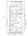
次に、図8および図9により、本実施の形態において、他のメモリカードを用いたシステムの構成の一例を説明する。図8および図9は、他のメモリカードを用いたシステムの構成図を示す。 Next, an example of a system configuration using another memory card in the present embodiment will be described with reference to FIGS. 8 and 9 show a configuration diagram of a system using other memory cards.
図8に示す、メモリカードを用いたシステムは、前記図1と同様にマルチメディアカードを用いたシステムとされ、前記図1に対して、フラッシュメモリ11aのI/O回路(
24)、コントローラ12aの電圧検出回路(34)を削除し、コントローラ12aのコ
ア回路31aを1.3V系で動作させるように構成した例である。
The system using the memory card shown in FIG. 8 is a system using a multimedia card as in FIG. 1, and is different from the system shown in FIG.
24) In this example, the voltage detection circuit (34) of the
この構成においては、コントローラ12aのレギュレータ35aが基準電圧発生回路を含み、ホスト機器2から1.8V系の電圧、または3.3V系の電圧が供給された場合でも、基準電圧発生回路により発生される基準電圧に基づいて、1.8V系および3.3V系のそれぞれの供給電圧に対応して1.3V系の電圧に降圧し、コア回路31aに対して1.3V系の電圧を供給して動作させることができる。なお、コントローラ12aのI/O回路32a,33a内のレベルシフタは、1.8V系の電圧であれば駆動させず、3.3V系の電圧であれば駆動させる。
In this configuration, the
また、フラッシュメモリ11aにおいては、レギュレータ23aが電圧検出回路を含み
、この電圧検出回路によりホスト機器2から供給された電源電圧を検出し、1.8V系の電圧レベルであれば、レギュレータ23aを駆動させないことで、メモリアレイ21aとロジック回路22aからなるコア回路を1.8V系動作モードで動作させることができ、また3.3V系の電圧レベルであれば、レギュレータ23aを駆動させて電圧レベルを変換することによって3.3V系動作モードで動作させることができる。
In the flash memory 11a, the
図9に示す、メモリカードを用いたシステムは、前記図1および前記図8と同様にマルチメディアカードを用いたシステムとされ、前記図8に対して、フラッシュメモリ11bのレギュレータ(23)を削除し、このフラッシュメモリ11bにコントローラ12bのレギュレータ35bで降圧した電圧を供給して1.8V系で動作させるとともに、コントローラ12bのコア回路31bも1.8V系で動作させるように構成した例である。
The system using a memory card shown in FIG. 9 is a system using a multimedia card as in FIG. 1 and FIG. 8, and the regulator (23) of the
この構成においては、コントローラ12bのレギュレータ35bが電圧検出回路を含み
、この電圧検出回路によりホスト機器2から供給された電源電圧を検出し、1.8V系の電圧レベルであれば、レギュレータ35bを駆動させずにコア回路31bを1.8V系動作モードで動作させ、また3.3V系の電圧レベルであれば、レギュレータ35bを駆動させて電圧レベルを変換して3.3V系動作モードで動作させることができる。なお、コントローラ12bのI/O回路32b,33b内のレベルシフタは、1.8V系の電圧であれば駆動させず、3.3V系の電圧であれば駆動させる。
In this configuration, the
また、フラッシュメモリ11bにおいては、コントローラ12bのレギュレータ35bを経由して1.8V系の電圧レベルが供給されるので、メモリアレイ21bとロジック回路22bからなるコア回路を1.8V系動作モードで動作させることができる。
In the
次に、図10により、本発明の一実施の形態である不揮発性メモリ混載マイコンを用いたシステムの構成の一例を説明する。図10は、不揮発性メモリ混載マイコンを用いたシステムの構成図を示す。 Next, with reference to FIG. 10, an example of the configuration of a system using a nonvolatile memory embedded microcomputer according to an embodiment of the present invention will be described. FIG. 10 shows a configuration diagram of a system using a nonvolatile memory embedded microcomputer.
本実施の形態である不揮発性メモリ混載マイコンを用いたシステムは、不揮発性メモリ混載マイコン6と、この不揮発性メモリ混載マイコン6に電気的に接続され、不揮発性メモリ混載マイコン6にコマンドを供給して、この不揮発性メモリ混載マイコン6の動作を制御するホスト機器7などから構成され、不揮発性メモリ混載マイコン6は前記メモリカードと同様の機能を有している。すなわち、不揮発性メモリ混載マイコン6は、各種情報を記憶するフラッシュメモリ61と、このフラッシュメモリ61に対する動作を制御するマイコン62などから構成される。
The system using the nonvolatile memory embedded microcomputer according to the present embodiment is electrically connected to the nonvolatile memory embedded
フラッシュメモリ61には、ユーザデータおよび管理データなどを記憶するメモリアレイ71と、このメモリアレイ71に対する制御論理機能を持つロジック回路72などが備えられている。このフラッシュメモリ61へは、マイコン62のレギュレータを経由して電源電圧が供給される。
The
マイコン62には、CPUおよびRAMなどからなるコア回路81と、ホスト機器7とのインターフェースを司り、ホスト機器7と接続するためのON/OFF機能付きのレベルシフタなどの制御論理機能を持つI/O回路82と、ホスト機器7から供給される電源電圧レベルを検出する電圧検出回路84と、コア回路81を動作させる電圧レベルを変換するためのON/OFF機能付きのレギュレータ85などが備えられている。
The
この構成において、不揮発性メモリ混載マイコン6に内蔵されたマイコン62が、ホスト機器7から供給される電源電圧レベルを判定する場合、1.8V系の電圧レベルに対応する検出点Aの通過判定後、3.3V系の電圧レベルに対応する検出点Bの通過有無を判定し、1.8V系の電圧レベルであれば、レギュレータ85、レベルシフタを駆動させずにフラッシュメモリ61に供給することにより、フラッシュメモリ61を1.8V系動作モードで動作させることができ、また3.3V系の電圧レベルであれば、レギュレータ85、レベルシフタを駆動させて電圧レベルを変換してフラッシュメモリ61に供給することにより、フラッシュメモリ61を3.3V系動作モードで動作させることができる。
In this configuration, when the
また、この不揮発性メモリ混載マイコン6において、ホスト機器7からの供給電圧が検出点Aを通過後に検出点Bを通過した時は、1.8V系から3.3V系の動作モードへ自動的に遷移可能であり、また検出点Bを通過後に検出点B以下に低下した時は、3.3V系から1.8V系の動作モードへ自動的に遷移可能な構成となっている。
In the nonvolatile memory embedded
従って、本実施の形態によれば、フラッシュメモリ11,11a,11bとコントローラ12,12a,12bを搭載したマルチメディアカード1,1a,1bや、フラッシュメモリ61とマイコン62を混載した不揮発性メモリ混載マイコン6において、1.8V系と3.3V系との異なる2種類の電源仕様により動作させることができる。
Therefore, according to the present embodiment, the multi-media cards 1, 1a, 1b on which the
また、マルチメディアカード1,1a,1bにおいては、1.8V系動作モードから3
.3V系動作モードへは自動的に遷移し、3.3V系動作モードから1.8V系動作モードへの遷移は不可能としたり、あるいはホスト機器2からのコマンドを受けて遷移可能とすることができる。
In the multimedia cards 1, 1a, 1b, the 1.8V system operation mode is changed to 3
. Transition to the 3V system operation mode automatically, transition from the 3.3V system operation mode to the 1.8V system operation mode is impossible, or it is possible to transition upon receiving a command from the
また、不揮発性メモリ混載マイコン6においては、1.8V系動作モードから3.3V系動作モードへの遷移、3.3V系動作モードから1.8V系動作モードへの遷移はどちらも自動的に可能とすることができる。
In the nonvolatile memory embedded
マルチメディアカードの内部レジスタとしてOCR(Operation Condition Register)と呼ばれるものがあり、そのOCRにはそのマルチメディアカードが動作可能な電圧を示す情報が含まれている。OCRの内容を表1に示す。 There is an OCR (Operation Condition Register) as an internal register of the multimedia card, and the OCR includes information indicating a voltage at which the multimedia card can operate. Table 1 shows the contents of OCR.

このOCRはマルチメディアカードに接続されるホスト機器からも読み出しが可能とされ、OCRに含まれる動作電圧情報を取得することにより、ホスト機器はマルチメディアカードが動作可能な電圧を知ることが出来、マルチメディアカードに供給する電圧レベルを選択することが可能となる。 This OCR can also be read from the host device connected to the multimedia card, and by obtaining the operating voltage information included in the OCR, the host device can know the voltage at which the multimedia card can operate. It is possible to select the voltage level supplied to the multimedia card.
ホスト機器からは、例えば1.8V系の動作電圧が供給されており、マルチメディアカード内のフラッシュメモリが1.8V系の動作電圧では格納されているデータの読み出しについても動作不安定となるようなフラッシュメモリであった場合を考慮すると、OCRをフラッシュメモリに格納していた場合、このようなフラッシュメモリから読み出されたOCR情報をホスト機器に供給した場合、誤った動作電圧情報をホスト機器は取得することにもなりかねないことから、OCR情報をフラッシュメモリに格納することは適切ではない。 For example, a 1.8 V system operating voltage is supplied from the host device, and the flash memory in the multimedia card is unstable even when reading stored data at the 1.8 V system operating voltage. If the OCR is stored in the flash memory, if the OCR information read from the flash memory is supplied to the host device, incorrect operating voltage information may be displayed on the host device. Storing the OCR information in the flash memory is not appropriate.
また、マルチメディアカード内のフラッシュメモリが1.8V系の動作電圧で動作可能か否かに応じて、OCR情報をフラッシュメモリに格納するか、他に格納するかを選択することは、マルチメディアカード内のコントローラの品種の増加を招き、製造コストの増大を招くことにもなる。 Also, depending on whether or not the flash memory in the multimedia card can be operated with an operating voltage of 1.8V system, it is possible to select whether the OCR information is stored in the flash memory or in other cases. This leads to an increase in the variety of controllers in the card, which also increases the manufacturing cost.
そこで、本発明者は、マルチメディアカードを2種類の電源により動作可能とすると共に、1種類の電源のみで動作可能とする場合においても、OCR情報を適切にホスト機器に供給することを検討した。 Therefore, the present inventor has considered that the OCR information can be appropriately supplied to the host device even when the multimedia card can be operated by two types of power sources and can be operated by only one type of power source. .
図11に、OCR情報の設定についての一実施の形態を示す。表1に示すOCRの内容のうち動作電圧を示す情報として設定を行う必要があるのは第7ビット目のみであり、他のビットについては固定となっている。そのため、第7ビットの設定のためにボンディングパットを設け、ボンディングパットが接地電源に接続されている場合は論理“0”に設定され、ボンディングパットがオープン又は動作電源に接続されている場合は論理“1”に設定され、マルチメディアカード全体として1.8V系の動作電圧で動作可能か否かを設定することが出来る。 FIG. 11 shows an embodiment for setting OCR information. Of the contents of the OCR shown in Table 1, only the seventh bit needs to be set as information indicating the operating voltage, and the other bits are fixed. Therefore, a bonding pad is provided for setting the seventh bit. When the bonding pad is connected to the ground power supply, the logic is set to “0”. When the bonding pad is open or connected to the operating power supply, the logic is set. It is set to “1”, and it is possible to set whether or not the multimedia card as a whole can be operated with an operating voltage of 1.8V system.
OCRの他のビットについても、将来において設定が必要となる可能性をも考慮するのであれば、図12に示す通り、他のビットについてもボンディングパットにより設定可能としておいても良い。 If consideration is given to the possibility of setting other bits in the OCR in the future, the other bits may be set by bonding pads as shown in FIG.
更に、図13に、OCR情報の設定についての他の実施の形態を示す。本実施の形態では、第7ビット目の設定のためにヒューズを設け、該ヒューズが電気的に接続されていることで接地電源に接続され論理“0”に設定され、該ヒューズが電気的に切断されていることで動作電源に接続され論理“1”に設定され、マルチメディアカード全体として1.8V系の動作電圧で動作可能か否かを設定することが出来る。 Further, FIG. 13 shows another embodiment for setting OCR information. In this embodiment, a fuse is provided for setting the seventh bit, and since the fuse is electrically connected, it is connected to the ground power supply and set to logic “0”. By being disconnected, it is connected to the operating power supply and set to logic “1”, and it can be set as to whether or not the entire multimedia card can be operated with an operating voltage of 1.8V system.
図12と同様、図14に示すように、OCRの他のビットについてもヒューズを介して接地電源若しくは動作電源のいずれか一方に接続しておくことで、設定可能としておいても良いことは言うまでもない。また、ヒューズの構成としてレーザで切断をするレーザヒューズ等や不揮発性メモリを用いたフラッシュヒューズ等であっても良い。 As in FIG. 12, as shown in FIG. 14, it goes without saying that other bits of the OCR may be settable by connecting them to either the ground power supply or the operating power supply via a fuse. Yes. Further, the fuse may be a laser fuse that is cut by a laser, a flash fuse that uses a nonvolatile memory, or the like.
また、ボンディングパットの接続電位やヒューズでの接続/切断の設定は、図示する様に動作電源にpull−upしている場合と、pull−downしている場合で異なることも言うまでもない。 Needless to say, the connection potential of the bonding pad and the connection / disconnection setting with the fuse are different depending on whether the operation power supply is pull-up or pull-down.
このように、OCR情報の設定をボンディングパットやヒューズにより設定可能とすることで、コントローラは接続されるフラッシュメモリの動作電圧に応じて設定可能とすることが出来、コントローラの品種の増加及び管理コストの増大を低減することが可能となる。 As described above, by setting the OCR information using a bonding pad or a fuse, the controller can be set according to the operating voltage of the connected flash memory. It is possible to reduce the increase in
以上、本発明者によってなされた発明を実施の形態に基づき具体的に説明したが、本発明は前記実施の形態に限定されるものではなく、その要旨を逸脱しない範囲で種々変更可能であることはいうまでもない。 As mentioned above, the invention made by the present inventor has been specifically described based on the embodiment. However, the present invention is not limited to the embodiment, and various modifications can be made without departing from the scope of the invention. Needless to say.
たとえば、前記実施の形態においては、不揮発性メモリとしてフラッシュメモリを例に説明したが、EEPROMなどの不揮発性メモリなどにも適用することが可能である。 For example, in the above embodiment, the flash memory has been described as an example of the nonvolatile memory, but the present invention can also be applied to a nonvolatile memory such as an EEPROM.
また、本発明は、前記のようにフラッシュメモリを搭載したマルチメディアカードに適用して効果的であるが、さらに他の規格のメモリカード、メモリ装置などの半導体装置全般に広く応用可能であり、特に異なる2種類の電源により動作させるメモリカードや半導体装置に良好に適用することができる。 Further, the present invention is effective when applied to a multimedia card equipped with a flash memory as described above, but can be widely applied to other semiconductor devices such as memory cards and memory devices of other standards, In particular, the present invention can be favorably applied to memory cards and semiconductor devices that are operated by two different types of power supplies.
更には、前記実施の形態では1.8V系動作モードと3.3V系動作モードの2つの動作モードについて説明をしたが、例えば1.2V系動作モードを更に有するようなメモリカードや半導体装置であっても良い。このようなメモリカードの場合、1.2V系の電源電圧が供給される場合は、レギュレータを停止させ又はスルーさせ、1.8V系又は3.3V系の電源電圧が供給される場合はレギュレータを動作させて、コア回路31等に1.2V系の電圧を供給するようにしても良い。
Furthermore, in the above-described embodiment, the two operation modes of the 1.8V system operation mode and the 3.3V system operation mode have been described. For example, in a memory card or a semiconductor device that further has a 1.2V system operation mode. There may be. In the case of such a memory card, when a 1.2V system power supply voltage is supplied, the regulator is stopped or through, and when a 1.8V system or 3.3V system power supply voltage is supplied, the regulator is turned off. It may be operated to supply a 1.2 V system voltage to the
若しくは、昇圧用のレギュレータと降圧用のレギュレータとを有し、1.8V系の電源電圧が供給される場合は、レギュレータを停止させ又はスルーさせ、1.2V系の電源電圧が供給される場合は昇圧用レギュレータを動作させ、3.3V系の電源電圧が供給される場合は降圧用レギュレータを動作させて、コア回路31等に1.8Vの電圧を供給するようにしても良い。
Alternatively, when a regulator for boosting and a regulator for stepping down are provided and a 1.8V system power supply voltage is supplied, the regulator is stopped or through and a 1.2V system power supply voltage is supplied May operate the step-up regulator, and when a 3.3V power supply voltage is supplied, operate the step-down regulator to supply a voltage of 1.8V to the
また、前記実施の形態では、フラッシュメモリは3.3V系の電源電圧を1.8V系の電源電圧にレギュレータで降圧してコア回路に供給しているが、メモリアレイ21に含まれるメモリセルへの書込や消去動作時において使用する例えば10V程度の高電圧を発生させる昇圧用のレギュレータを更に有しても良い。 In the above-described embodiment, the flash memory supplies a 3.3 V power supply voltage to the 1.8 V power supply voltage by a regulator and supplies it to the core circuit. A boosting regulator that generates a high voltage of about 10 V, for example, used during the write and erase operations may be further included.
1,1a,1b マルチメディアカード
2 ホスト機器
11,11a,11b フラッシュメモリ
12,12a,12b コントローラ
21,21a,21b メモリアレイ
22,22a,22b ロジック回路
23,23a レギュレータ
24 I/O回路
31,31a,31b コア回路
32,32a,32b I/O回路
33,33a,33b I/O回路
34 電圧検出回路
35,35a,35b レギュレータ
6 不揮発性メモリ混載マイコン
7 ホスト機器
61 フラッシュメモリ
62 マイコン
71 メモリアレイ
72 ロジック回路
81 コア回路
82 I/O回路
84 電圧検出回路
85 レギュレータ
1, 1a,
Claims (7)
前記不揮発性メモリ乃至前記制御手段の少なくともどちらか一方に、前記不揮発性メモリの動作に対応して電圧レベルを変換する変換手段を備え、
前記不揮発性メモリを第1電圧レベルで動作させる第1動作モードと、前記不揮発性メモリを前記第1電圧レベルより高い第2電圧レベルで動作させる第2動作モードとを有し、
前記制御手段は、供給される電源電圧レベルを判定する場合、前記第1電圧レベルに対応する第1検出点の通過判定後、前記第2電圧レベルに対応する第2検出点の通過有無を判定し、前記第1電圧レベルであれば前記変換手段を駆動させずに前記不揮発性メモリを前記第1動作モードで動作させ、前記第2電圧レベルであれば前記変換手段を駆動させて電圧レベルを変換して前記不揮発性メモリを前記第2動作モードで動作させるものであり、
前記制御手段は、前記第1動作モードから前記第2動作モードへの遷移は自動的に行い、前記第2動作モードから前記第1動作モードへの遷移は不可能とすることを特徴とするメモリカード。 A non-volatile memory, and control means for controlling the operation of the non-volatile memory,
At least one of the non-volatile memory and the control unit includes a conversion unit that converts a voltage level corresponding to the operation of the non-volatile memory,
A first operation mode in which the nonvolatile memory is operated at a first voltage level; and a second operation mode in which the nonvolatile memory is operated at a second voltage level higher than the first voltage level;
When determining the power supply voltage level to be supplied, the control means determines whether or not the second detection point corresponding to the second voltage level has passed after the passage determination of the first detection point corresponding to the first voltage level. If it is the first voltage level, the non-volatile memory is operated in the first operation mode without driving the conversion means, and if it is the second voltage level, the conversion means is driven to set the voltage level. Converting the non-volatile memory to operate in the second operation mode;
The control means automatically performs a transition from the first operation mode to the second operation mode, and makes a transition from the second operation mode to the first operation mode impossible. card.
前記不揮発性メモリ乃至前記制御手段の少なくともどちらか一方に、前記不揮発性メモリの動作に対応して電圧レベルを変換する変換手段を備え、
前記不揮発性メモリを第1電圧レベルで動作させる第1動作モードと、前記不揮発性メモリを前記第1電圧レベルより高い第2電圧レベルで動作させる第2動作モードとを有し、
前記制御手段は、供給される電源電圧レベルを判定する場合、前記第1電圧レベルに対応する第1検出点の通過判定後、前記第2電圧レベルに対応する第2検出点の通過有無を判定し、前記第1電圧レベルであれば前記変換手段を駆動させずに前記不揮発性メモリを前記第1動作モードで動作させ、前記第2電圧レベルであれば前記変換手段を駆動させて電圧レベルを変換して前記不揮発性メモリを前記第2動作モードで動作させるものであり、
前記制御手段は、前記第1動作モードから前記第2動作モードへの遷移は自動的に行い、前記第2動作モードから前記第1動作モードへの遷移はホスト機器からの遷移指示を受けて可能とすることを特徴とするメモリカード。 A non-volatile memory, and control means for controlling the operation of the non-volatile memory,
At least one of the non-volatile memory and the control unit includes a conversion unit that converts a voltage level corresponding to the operation of the non-volatile memory,
A first operation mode in which the nonvolatile memory is operated at a first voltage level; and a second operation mode in which the nonvolatile memory is operated at a second voltage level higher than the first voltage level;
When determining the power supply voltage level to be supplied, the control means determines whether or not the second detection point corresponding to the second voltage level has passed after the passage determination of the first detection point corresponding to the first voltage level. If it is the first voltage level, the non-volatile memory is operated in the first operation mode without driving the conversion means, and if it is the second voltage level, the conversion means is driven to set the voltage level. Converting the non-volatile memory to operate in the second operation mode;
The control means automatically performs a transition from the first operation mode to the second operation mode, and a transition from the second operation mode to the first operation mode is possible upon receiving a transition instruction from a host device. A memory card characterized by that.
前記制御手段は、前記第1電圧レベルと前記第2電圧レベルのいずれか一方、または両方で動作可能を示す情報を持つことを特徴とするメモリカード。 The memory card according to claim 1, wherein:
The memory card having information indicating that the control means can operate at one or both of the first voltage level and the second voltage level.
前記第1電圧レベルは1.8V系であり、前記第2電圧レベルは3.3V系であることを特徴とするメモリカード。 The memory card according to claim 1, wherein:
The memory card according to claim 1, wherein the first voltage level is a 1.8V system, and the second voltage level is a 3.3V system.
前記マイコンに、前記不揮発性メモリの動作に対応して電圧レベルを変換する変換手段を備え、
前記不揮発性メモリを第1電圧レベルで動作させる第1動作モードと、前記不揮発性メモリを前記第1電圧レベルより高い第2電圧レベルで動作させる第2動作モードとを有し、
前記マイコンは、供給される電源電圧レベルを判定する場合、前記第1電圧レベルに対応する第1検出点の通過判定後、前記第2電圧レベルに対応する第2検出点の通過有無を判定し、前記第1電圧レベルであれば前記変換手段を駆動させずに前記不揮発性メモリを前記第1動作モードで動作させ、前記第2電圧レベルであれば前記変換手段を駆動させて電圧レベルを変換して前記不揮発性メモリを前記第2動作モードで動作させるものであり、
前記マイコンは、前記第1動作モードから前記第2動作モードへの遷移、および前記第2動作モードから前記第1動作モードへの遷移は自動的に行うことを特徴とする不揮発性メモリ混載マイコン。 A non-volatile memory, and a microcomputer for controlling the operation of the non-volatile memory,
The microcomputer includes conversion means for converting a voltage level corresponding to the operation of the nonvolatile memory,
A first operation mode in which the nonvolatile memory is operated at a first voltage level; and a second operation mode in which the nonvolatile memory is operated at a second voltage level higher than the first voltage level;
When determining the power supply voltage level to be supplied, the microcomputer determines whether or not the second detection point corresponding to the second voltage level has passed after the passage determination of the first detection point corresponding to the first voltage level. If the first voltage level, the non-volatile memory is operated in the first operation mode without driving the conversion means, and if the second voltage level, the conversion means is driven to convert the voltage level. And operating the non-volatile memory in the second operation mode,
A microcomputer with embedded nonvolatile memory, wherein the microcomputer automatically performs transition from the first operation mode to the second operation mode and transition from the second operation mode to the first operation mode.
前記マイコンは、前記第1電圧レベルと前記第2電圧レベルのいずれか一方、または両方で動作可能を示す情報を持つことを特徴とする不揮発性メモリ混載マイコン。 The nonvolatile memory embedded microcomputer according to claim 5,
The microcomputer includes information indicating that the microcomputer can operate at one or both of the first voltage level and the second voltage level.
前記第1電圧レベルは1.8V系であり、前記第2電圧レベルは3.3V系であることを特徴とする不揮発性メモリ混載マイコン。 The nonvolatile memory embedded microcomputer according to claim 5,
The microcomputer with embedded nonvolatile memory, wherein the first voltage level is 1.8V system and the second voltage level is 3.3V system.
Priority Applications (6)
| Application Number | Priority Date | Filing Date | Title |
|---|---|---|---|
| JP2004080593A JP4653960B2 (en) | 2003-08-07 | 2004-03-19 | Memory card and nonvolatile memory embedded microcomputer |
| TW093118806A TW200508981A (en) | 2003-08-07 | 2004-06-28 | Memory card and non-volatile memory consolidated microprocessor |
| US10/891,297 US6982919B2 (en) | 2003-08-07 | 2004-07-15 | Memory card and data processing system |
| CN200410054926.5A CN1581357A (en) | 2003-08-07 | 2004-07-21 | Storage card and data processing system |
| KR1020040059146A KR20050016024A (en) | 2003-08-07 | 2004-07-28 | Memory card and microcomputer with non-volatile memory |
| US11/271,957 US7161834B2 (en) | 2003-08-07 | 2005-11-14 | Memory card and data processing system |
Applications Claiming Priority (2)
| Application Number | Priority Date | Filing Date | Title |
|---|---|---|---|
| JP2003288407 | 2003-08-07 | ||
| JP2004080593A JP4653960B2 (en) | 2003-08-07 | 2004-03-19 | Memory card and nonvolatile memory embedded microcomputer |
Publications (2)
| Publication Number | Publication Date |
|---|---|
| JP2005071325A JP2005071325A (en) | 2005-03-17 |
| JP4653960B2 true JP4653960B2 (en) | 2011-03-16 |
Family
ID=34197136
Family Applications (1)
| Application Number | Title | Priority Date | Filing Date |
|---|---|---|---|
| JP2004080593A Expired - Fee Related JP4653960B2 (en) | 2003-08-07 | 2004-03-19 | Memory card and nonvolatile memory embedded microcomputer |
Country Status (5)
| Country | Link |
|---|---|
| US (2) | US6982919B2 (en) |
| JP (1) | JP4653960B2 (en) |
| KR (1) | KR20050016024A (en) |
| CN (1) | CN1581357A (en) |
| TW (1) | TW200508981A (en) |
Families Citing this family (37)
| Publication number | Priority date | Publication date | Assignee | Title |
|---|---|---|---|---|
| KR100884235B1 (en) * | 2003-12-31 | 2009-02-17 | 삼성전자주식회사 | Nonvolatile memory card |
| KR100606157B1 (en) * | 2004-07-26 | 2006-08-01 | 삼성전자주식회사 | Flash memory with power level sensing circuit |
| US7864615B2 (en) * | 2005-02-25 | 2011-01-04 | Kingston Technology Corporation | Flash memory controller utilizing multiple voltages and a method of use |
| CN101167038A (en) * | 2005-04-27 | 2008-04-23 | 松下电器产业株式会社 | Card-type electronic device and host device |
| TWI319160B (en) * | 2005-07-11 | 2010-01-01 | Via Tech Inc | Memory card capable of supporting various voltage supply and control chip and method of supporting voltage thereof |
| KR100703885B1 (en) | 2005-07-18 | 2007-04-06 | 삼성전자주식회사 | Apparatus and method for generating internal voltage adaptively from external supply voltage |
| CN100535831C (en) * | 2005-07-26 | 2009-09-02 | 威盛电子股份有限公司 | Memory card and memory control chip supporting multiple voltage supply and voltage supply method |
| TW200723289A (en) * | 2005-12-09 | 2007-06-16 | A Data Technology Co Ltd | Non-volatile memory storage device and controller thereof |
| US7702935B2 (en) * | 2006-01-25 | 2010-04-20 | Apple Inc. | Reporting flash memory operating voltages |
| US20070174641A1 (en) * | 2006-01-25 | 2007-07-26 | Cornwell Michael J | Adjusting power supplies for data storage devices |
| US7861122B2 (en) * | 2006-01-27 | 2010-12-28 | Apple Inc. | Monitoring health of non-volatile memory |
| KR101177555B1 (en) * | 2006-02-01 | 2012-08-27 | 삼성전자주식회사 | Memory Card and DATA driving Method thereof and Memory Card System |
| TWI301276B (en) * | 2006-06-16 | 2008-09-21 | A Data Technology Co Ltd | Non-volatile storage apparatus and method for controlling the same |
| US7516293B2 (en) * | 2006-09-08 | 2009-04-07 | International Business Machines Corporation | Increased performance using mixed memory types |
| JP4851962B2 (en) * | 2007-02-28 | 2012-01-11 | 株式会社東芝 | Memory system |
| US20080288712A1 (en) | 2007-04-25 | 2008-11-20 | Cornwell Michael J | Accessing metadata with an external host |
| US7913032B1 (en) | 2007-04-25 | 2011-03-22 | Apple Inc. | Initiating memory wear leveling |
| JP2009053970A (en) * | 2007-08-28 | 2009-03-12 | Toshiba Corp | Semiconductor device |
| US8067861B2 (en) * | 2008-02-29 | 2011-11-29 | Panasonic Corporation | Interface device for host device, interface device for slave device, host device, slave device, communication system and interface voltage switching method |
| JP5106219B2 (en) * | 2008-03-19 | 2012-12-26 | 株式会社東芝 | Memory device, host device, memory system, memory device control method, host device control method, and memory system control method |
| US20100262979A1 (en) * | 2009-04-08 | 2010-10-14 | Google Inc. | Circular command queues for communication between a host and a data storage device |
| US8447918B2 (en) | 2009-04-08 | 2013-05-21 | Google Inc. | Garbage collection for failure prediction and repartitioning |
| US20100287217A1 (en) * | 2009-04-08 | 2010-11-11 | Google Inc. | Host control of background garbage collection in a data storage device |
| US8205037B2 (en) * | 2009-04-08 | 2012-06-19 | Google Inc. | Data storage device capable of recognizing and controlling multiple types of memory chips operating at different voltages |
| JP5789759B2 (en) * | 2010-03-16 | 2015-10-07 | パナソニックIpマネジメント株式会社 | Information processing apparatus, nonvolatile storage device, information processing system, and nonvolatile memory controller |
| US20130227197A1 (en) * | 2012-02-29 | 2013-08-29 | Sandisk Technologies Inc. | Multiple pre-driver logic for io high speed interfaces |
| CN103869885A (en) * | 2012-12-18 | 2014-06-18 | 鸿富锦精密工业(深圳)有限公司 | Expansion card and mainboard supporting expansion card |
| CN104035827A (en) * | 2013-03-08 | 2014-09-10 | 鸿富锦精密工业(深圳)有限公司 | Electronic device |
| US9042172B2 (en) * | 2013-05-02 | 2015-05-26 | Windbond Electronics Corporation | Flash memory having dual supply operation |
| US9483096B2 (en) * | 2013-12-06 | 2016-11-01 | Sandisk Technologies Llc | Host interface of a memory device supplied with regulated or non-regulated power based on operating mode of the memory device |
| TWI529721B (en) * | 2014-05-06 | 2016-04-11 | 群聯電子股份有限公司 | Memory storage device, memory control circuit unit and power supply method |
| JP6413077B2 (en) * | 2014-10-10 | 2018-10-31 | パナソニックIpマネジメント株式会社 | Host device, slave device, interface semiconductor device, and removable system |
| JP6620313B2 (en) * | 2016-01-06 | 2019-12-18 | パナソニックIpマネジメント株式会社 | Host device, slave device and removable system |
| US9817601B1 (en) * | 2016-07-07 | 2017-11-14 | Nxp Usa, Inc. | Method and apparatus for determining feasibility of memory operating condition change using different back bias voltages |
| US10061378B2 (en) * | 2016-07-29 | 2018-08-28 | Sandisk Technologies Llc | System and method for adjusting device performance based on sensed host current sourcing capability |
| CN109284808B (en) * | 2018-09-13 | 2024-08-20 | 华为技术有限公司 | Multimedia storage card and mobile electronic device |
| JP7494071B2 (en) * | 2020-09-23 | 2024-06-03 | キオクシア株式会社 | Memory System |
Family Cites Families (9)
| Publication number | Priority date | Publication date | Assignee | Title |
|---|---|---|---|---|
| US202383A (en) * | 1878-04-16 | Improvement in riding corn-cultivators | ||
| JP3222243B2 (en) * | 1993-01-25 | 2001-10-22 | 株式会社日立製作所 | Semiconductor storage device and information processing system using the same |
| JP3477781B2 (en) | 1993-03-23 | 2003-12-10 | セイコーエプソン株式会社 | IC card |
| JPH09231339A (en) | 1996-02-27 | 1997-09-05 | Mitsubishi Electric Corp | Memory card |
| US5909449A (en) * | 1997-09-08 | 1999-06-01 | Invox Technology | Multibit-per-cell non-volatile memory with error detection and correction |
| JP4229482B2 (en) * | 1997-10-24 | 2009-02-25 | 株式会社ルネサステクノロジ | Microcomputer with built-in flash memory |
| JP2000250665A (en) * | 1999-02-26 | 2000-09-14 | Hitachi Ltd | Semiconductor integrated circuit and memory card |
| JP4082913B2 (en) * | 2002-02-07 | 2008-04-30 | 株式会社ルネサステクノロジ | Memory system |
| TW595786U (en) * | 2003-06-11 | 2004-06-21 | C One Technology Corp | Micro electronic card with a plurality of different communication interfaces |
-
2004
- 2004-03-19 JP JP2004080593A patent/JP4653960B2/en not_active Expired - Fee Related
- 2004-06-28 TW TW093118806A patent/TW200508981A/en not_active IP Right Cessation
- 2004-07-15 US US10/891,297 patent/US6982919B2/en not_active Expired - Lifetime
- 2004-07-21 CN CN200410054926.5A patent/CN1581357A/en active Pending
- 2004-07-28 KR KR1020040059146A patent/KR20050016024A/en not_active Withdrawn
-
2005
- 2005-11-14 US US11/271,957 patent/US7161834B2/en not_active Expired - Lifetime
Also Published As
| Publication number | Publication date |
|---|---|
| US6982919B2 (en) | 2006-01-03 |
| TWI336052B (en) | 2011-01-11 |
| JP2005071325A (en) | 2005-03-17 |
| US20050041509A1 (en) | 2005-02-24 |
| US7161834B2 (en) | 2007-01-09 |
| KR20050016024A (en) | 2005-02-21 |
| US20060062052A1 (en) | 2006-03-23 |
| TW200508981A (en) | 2005-03-01 |
| CN1581357A (en) | 2005-02-16 |
Similar Documents
| Publication | Publication Date | Title |
|---|---|---|
| JP4653960B2 (en) | Memory card and nonvolatile memory embedded microcomputer | |
| US10460775B2 (en) | Asynchronous/synchronous interface | |
| US7092308B2 (en) | Portable data storage apparatus | |
| JP4734243B2 (en) | Voltage regulator with bypass for a multi-stage voltage storage system | |
| JP4488800B2 (en) | Semiconductor integrated circuit device | |
| KR101780421B1 (en) | Nonvolatile memory device, wordline voltage generating method, programming method and reading method thereof, memory system and electronic device having the same | |
| US6798709B2 (en) | Memory device having dual power ports and memory system including the same | |
| EP1513070B1 (en) | System having insertable and removable storage and a control method thereof | |
| US8493795B2 (en) | Voltage stabilization device and semiconductor device including the same, and voltage generation method | |
| JP2010518544A (en) | Nonvolatile semiconductor memory having multiple external power supply units | |
| US7366019B2 (en) | Nonvolatile memory | |
| US20080046640A1 (en) | Memory system with reduced standby current | |
| CN111383671B (en) | Semiconductor device and power supply control method thereof | |
| KR100746246B1 (en) | Memory card having power selection switch and its operation method |
Legal Events
| Date | Code | Title | Description |
|---|---|---|---|
| A621 | Written request for application examination |
Free format text: JAPANESE INTERMEDIATE CODE: A621 Effective date: 20070312 |
|
| A977 | Report on retrieval |
Free format text: JAPANESE INTERMEDIATE CODE: A971007 Effective date: 20091222 |
|
| A131 | Notification of reasons for refusal |
Free format text: JAPANESE INTERMEDIATE CODE: A131 Effective date: 20100209 |
|
| A521 | Request for written amendment filed |
Free format text: JAPANESE INTERMEDIATE CODE: A523 Effective date: 20100408 |
|
| A711 | Notification of change in applicant |
Free format text: JAPANESE INTERMEDIATE CODE: A712 Effective date: 20100528 |
|
| TRDD | Decision of grant or rejection written | ||
| A01 | Written decision to grant a patent or to grant a registration (utility model) |
Free format text: JAPANESE INTERMEDIATE CODE: A01 Effective date: 20101124 |
|
| A01 | Written decision to grant a patent or to grant a registration (utility model) |
Free format text: JAPANESE INTERMEDIATE CODE: A01 |
|
| A61 | First payment of annual fees (during grant procedure) |
Free format text: JAPANESE INTERMEDIATE CODE: A61 Effective date: 20101220 |
|
| R150 | Certificate of patent or registration of utility model |
Ref document number: 4653960 Country of ref document: JP Free format text: JAPANESE INTERMEDIATE CODE: R150 Free format text: JAPANESE INTERMEDIATE CODE: R150 |
|
| FPAY | Renewal fee payment (event date is renewal date of database) |
Free format text: PAYMENT UNTIL: 20131224 Year of fee payment: 3 |
|
| S531 | Written request for registration of change of domicile |
Free format text: JAPANESE INTERMEDIATE CODE: R313531 |
|
| R350 | Written notification of registration of transfer |
Free format text: JAPANESE INTERMEDIATE CODE: R350 |
|
| LAPS | Cancellation because of no payment of annual fees |