JP4615197B2 - Manufacturing method of TFT array substrate and manufacturing method of liquid crystal display device - Google Patents
Manufacturing method of TFT array substrate and manufacturing method of liquid crystal display device Download PDFInfo
- Publication number
- JP4615197B2 JP4615197B2 JP2003207744A JP2003207744A JP4615197B2 JP 4615197 B2 JP4615197 B2 JP 4615197B2 JP 2003207744 A JP2003207744 A JP 2003207744A JP 2003207744 A JP2003207744 A JP 2003207744A JP 4615197 B2 JP4615197 B2 JP 4615197B2
- Authority
- JP
- Japan
- Prior art keywords
- electrode
- forming
- semiconductor layer
- layer
- droplet
- Prior art date
- Legal status (The legal status is an assumption and is not a legal conclusion. Google has not performed a legal analysis and makes no representation as to the accuracy of the status listed.)
- Expired - Fee Related
Links
Images


Classifications
-
- H—ELECTRICITY
- H10—SEMICONDUCTOR DEVICES; ELECTRIC SOLID-STATE DEVICES NOT OTHERWISE PROVIDED FOR
- H10D—INORGANIC ELECTRIC SEMICONDUCTOR DEVICES
- H10D30/00—Field-effect transistors [FET]
- H10D30/01—Manufacture or treatment
- H10D30/021—Manufacture or treatment of FETs having insulated gates [IGFET]
- H10D30/031—Manufacture or treatment of FETs having insulated gates [IGFET] of thin-film transistors [TFT]
- H10D30/0312—Manufacture or treatment of FETs having insulated gates [IGFET] of thin-film transistors [TFT] characterised by the gate electrodes
- H10D30/0316—Manufacture or treatment of FETs having insulated gates [IGFET] of thin-film transistors [TFT] characterised by the gate electrodes of lateral bottom-gate TFTs comprising only a single gate
-
- H—ELECTRICITY
- H10—SEMICONDUCTOR DEVICES; ELECTRIC SOLID-STATE DEVICES NOT OTHERWISE PROVIDED FOR
- H10D—INORGANIC ELECTRIC SEMICONDUCTOR DEVICES
- H10D30/00—Field-effect transistors [FET]
- H10D30/01—Manufacture or treatment
- H10D30/021—Manufacture or treatment of FETs having insulated gates [IGFET]
- H10D30/031—Manufacture or treatment of FETs having insulated gates [IGFET] of thin-film transistors [TFT]
- H10D30/0321—Manufacture or treatment of FETs having insulated gates [IGFET] of thin-film transistors [TFT] comprising silicon, e.g. amorphous silicon or polysilicon
-
- H—ELECTRICITY
- H10—SEMICONDUCTOR DEVICES; ELECTRIC SOLID-STATE DEVICES NOT OTHERWISE PROVIDED FOR
- H10D—INORGANIC ELECTRIC SEMICONDUCTOR DEVICES
- H10D30/00—Field-effect transistors [FET]
- H10D30/60—Insulated-gate field-effect transistors [IGFET]
- H10D30/67—Thin-film transistors [TFT]
- H10D30/6704—Thin-film transistors [TFT] having supplementary regions or layers in the thin films or in the insulated bulk substrates for controlling properties of the device
- H10D30/6723—Thin-film transistors [TFT] having supplementary regions or layers in the thin films or in the insulated bulk substrates for controlling properties of the device having light shields
-
- H—ELECTRICITY
- H10—SEMICONDUCTOR DEVICES; ELECTRIC SOLID-STATE DEVICES NOT OTHERWISE PROVIDED FOR
- H10D—INORGANIC ELECTRIC SEMICONDUCTOR DEVICES
- H10D30/00—Field-effect transistors [FET]
- H10D30/60—Insulated-gate field-effect transistors [IGFET]
- H10D30/67—Thin-film transistors [TFT]
- H10D30/6729—Thin-film transistors [TFT] characterised by the electrodes
- H10D30/673—Thin-film transistors [TFT] characterised by the electrodes characterised by the shapes, relative sizes or dispositions of the gate electrodes
-
- H—ELECTRICITY
- H10—SEMICONDUCTOR DEVICES; ELECTRIC SOLID-STATE DEVICES NOT OTHERWISE PROVIDED FOR
- H10D—INORGANIC ELECTRIC SEMICONDUCTOR DEVICES
- H10D30/00—Field-effect transistors [FET]
- H10D30/60—Insulated-gate field-effect transistors [IGFET]
- H10D30/67—Thin-film transistors [TFT]
- H10D30/674—Thin-film transistors [TFT] characterised by the active materials
-
- H—ELECTRICITY
- H10—SEMICONDUCTOR DEVICES; ELECTRIC SOLID-STATE DEVICES NOT OTHERWISE PROVIDED FOR
- H10D—INORGANIC ELECTRIC SEMICONDUCTOR DEVICES
- H10D30/00—Field-effect transistors [FET]
- H10D30/60—Insulated-gate field-effect transistors [IGFET]
- H10D30/67—Thin-film transistors [TFT]
- H10D30/6757—Thin-film transistors [TFT] characterised by the structure of the channel, e.g. transverse or longitudinal shape or doping profile
-
- H—ELECTRICITY
- H10—SEMICONDUCTOR DEVICES; ELECTRIC SOLID-STATE DEVICES NOT OTHERWISE PROVIDED FOR
- H10D—INORGANIC ELECTRIC SEMICONDUCTOR DEVICES
- H10D86/00—Integrated devices formed in or on insulating or conducting substrates, e.g. formed in silicon-on-insulator [SOI] substrates or on stainless steel or glass substrates
- H10D86/01—Manufacture or treatment
- H10D86/021—Manufacture or treatment of multiple TFTs
- H10D86/0241—Manufacture or treatment of multiple TFTs using liquid deposition, e.g. printing
Landscapes
- Liquid Crystal (AREA)
- Thin Film Transistor (AREA)
- Electrodes Of Semiconductors (AREA)
- Electroluminescent Light Sources (AREA)
- Internal Circuitry In Semiconductor Integrated Circuit Devices (AREA)
Description
【0001】
【発明の属する技術分野】
本発明は、TFTアレイ基板、液晶表示装置、TFTアレイ基板の製造方法および液晶表示装置の製造方法に関するものである。
【0002】
【従来の技術】
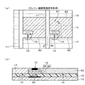
従来、TFT(Thin Film Transistor、薄膜トランジスタ)を備えた液晶表示装置において、TFTアレイ基板は、図28に示す一連の工程により製造されている。即ち、従来のTFTアレイ基板の製造工程は、ゲート線成膜、ゲート線形成、ゲート絶縁層成膜・半導体層成膜、半導体層形成、ソース・ドレイン線成膜、ソース・ドレイン線形成、チャネル部加工、保護膜形成、保護膜加工、画素電極成膜および画素電極形成の各工程(101〜111)からなる。
【0003】
上記のゲート線形成工程102、半導体層形成工程104、ソース・ドレイン線形成工程106、保護膜加工工程109および画素電極形成工程111の5つの工程では、マスクを使用したフォトリソグラフィ工程およびエッチング工程を含んでいる。即ち、これら工程では、これら工程の前段の工程であるゲート線成膜工程101、ゲート絶縁層成膜・半導体層成膜工程103、ソース・ドレイン線成膜工程105、保護膜形成工程108、画素電極成膜工程110において形成された膜をマスクを使用したフォトリソグラフィ工程およびエッチング工程によって加工している。
【0004】
一方、近年においては、フォトリソグラフィを使用せず、インクジェット方式により配線を形成する技術が提案されている。この技術では、例えば特許文献1(特開平11−204529号公報)に開示されているように、配線を形成する基板上に、配線形成材料に対する親和領域と非親和領域とを形成し、親和領域にインクジェット方式にて配線材料の液滴を滴下することにより配線を形成するものとなっている。
【0005】
また、特許文献2(特開2000−353594号公報)には、同様にインクジェット方式による配線形成技術において、配線形成領域からの配線材料のはみ出しを抑制するために、配線形成領域の両側にバンクを形成し、このバンクの上部を非親液性とし、配線形成領域を親液性とすることが開示されている。
【0006】
また、非特許文献1(SID 01 DIGEST の第40〜第43頁、6.1: Invited Paper: All-Polymer Thin Film Transistors Fabricated by High-Resolution Ink-jet Printing (著者 Takeo kawase 他))には、インクジェット方式を使用し、全て有機物を材料としてTFTを形成する技術が開示されている。
【0007】
【特許文献1】
特開平11−204529号公報(1999年7月30日公開)
【0008】
【特許文献2】
特開2000−353594号公報(2000年12月19日公開)
【0009】
【非特許文献1】
SID 01 DIGEST の第40〜第43頁、6.1: Invited Paper: All-Polymer Thin Film Transistors Fabricated by High-Resolution Ink-jet Printing(著者 Takeo kawase 他)、2001年
【0010】
【発明が解決しようとする課題】
従来のフォトリソグラフィを使用したTFTアレイ基板の製造方法では、上記のように、ゲート線形成工程102、半導体層形成工程104、ソース・ドレイン線形成工程106、保護膜加工工程109および画素電極形成工程111の少なくとも5つの工程においてマスクが必要となる。また、各成膜工程に使用される成膜装置および成膜の加工(形成・加工工程)に使用される加工装置は全て真空装置を使用している。したがって、近年さらなる大型化が要望されている液晶表示装置の大型基板にTFTを形成するには莫大な設備費が必要となる。
【0011】
また、基板の大型化に伴って、レジスト、配線材料の使用量が増加している。
一方、配線の形成などの加工においては、レジストを始めとして各材料はエッチングや剥離工程によって殆どが除去、廃棄されており、有効利用が図られていない。このため、廃棄処理や廃棄費用も基板の大型化によって大幅に増加しており、さらに廃棄物によって環境負荷が大きくなっている。このように、主としてフォトリソグラフィを多数含むTFTアレイ基板の製造方法は、製造工数増およびコストアップを招来するものとなっている。
【0012】
一方、例えば上記の従来文献に開示されているインクジェット方式利用すれば、TFTアレイ基板の上記製造工程において、必要なマスク数を減少させることができる。そこで、例えばインクジェット方式を利用し、製造工数の低減およびコストダウンが可能な技術の開発が求められていた。
【0013】
【課題を解決するための手段】
上記の課題を解決するために、本発明のTFTアレイ基板は、基板上にゲート電極が形成され、このゲート電極上に、ゲート絶縁層を介して半導体層が形成された薄膜トランジスタ部を備えているTFTアレイ基板において、前記半導体層が液滴の滴下形状をなしていることを特徴としている。
【0014】
上記の構成によれば、半導体層が液滴の滴下形状(例えばほぼ円形や円をずらしながら重ね合わせたような形状等)をなしているので、半導体層をインクジェット方式を利用した半導体材料の液滴の例えば1滴の滴下により形成することが可能となる。あるいは、インクジェット方式を利用し、例えばレジスト材料の液滴の例えば1滴を半導体成膜の上に滴下してレジスト層を形成し、このレジスト層をマスクとして半導体成膜を加工し、半導体層を形成することが可能となる。
あるいは、インクジェット方式を利用し、レジスト材料に代えて導電性材料の液滴を用いて導電体成膜層を形成し、これをマスクとして同様に半導体層を形成することが可能となる。
【0015】
このような方式によれば、TFTアレイ基板の製造において、半導体層を形成するためのマスクが不要となり、必要なマスク数が減少する結果、製造工数を削減することができる。また、マスクを使用したフォトリソグラフィ工程が減少するので、フォトリソグラフィ工程のための設備費の削減が可能であるのに加えて、廃棄される材料の量が減少する。これにより、製造時間の短縮およびコストダウンが可能となる。
【0016】
なお、半導体材料やレジスト材料、導電性材料の滴下には、上記インクジェット方式に限らず、材料の液滴の滴下により半導体層やレジスト層、導電体成膜層を直接形成可能な方式であれば使用可能である。
【0017】
上記のTFTアレイ基板は、前記薄膜トランジスタ部のゲート電極が、ゲート電極における本線からの分岐電極であり、前記分岐電極における開放端が前記半導体層の領域から突出している構成としてもよい。
【0018】
上記の構成によれば、薄膜トランジスタ部における、ゲート電極の分岐電極は、半導体層の領域から開放端が突出した形状となっているので、分岐電極からの電界の作用により、ソース・ドレイン電極間のリーク電流を適切に抑制することができる。
【0019】
上記のように、ゲート電極の分岐電極が、半導体層の領域から開放端が突出するように形成すれば、透過型液晶表示装置のようにTFTアレイ基板の画素部が透明な場合、突出した開放端が画素部にかかり開口率を低下させる虞がある。なお、反射型液晶表示装置に適用されるTFTアレイ基板の場合には、上記のような開口率の問題を考慮する必要はないので、分岐電極の設計の自由度が増す。
【0020】
そこで、本発明のTFTアレイ基板は、前記分岐電極の、前記半導体層の領域から突出している部分の幅を、該半導体層の領域内の部分の幅よりも小さくなるように形成した構成としてもよい。
【0021】
上記の構成によれば、画素部にかかる分岐電極の開放端が該画素部に占める割合が小さくなり、開口率の低下を抑制できる。
【0022】
また、本発明のTFTアレイ基板は、前記半導体層の上には、ソース電極とドレイン電極とが形成され、かつこれら両電極間にチャネル部が形成され、前記分岐電極の、前記半導体層の領域から突出している部分は、前記ソース電極またはドレイン電極の何れか一方に近接して形成された構成としてもよい。
【0023】
上記の構成によれば、分岐電極の、前記半導体層の領域から突出している部分を、ソース電極またはドレイン電極の何れか一方に近接して形成することで、TFTアレイ基板の画素部内で、開口率を低下させることなく、該分岐電極の開放端の突出部分を延ばして形成することができる。
【0024】
これにより、半導体層の領域から分岐電極の開放端を確実に突出させた状態にすることができるので、ソース・ドレイン電極間のリーク電流を確実に抑制することができる。
【0025】
この結果、薄膜トランジスタの特性を向上させることが可能となる。
【0026】
また、前記分岐電極の、前記半導体層の領域から突出している部分は、以下のようにして規定することが考えられる。
【0027】
すなわち、本発明のTFTアレイ基板は、前記半導体層の上には、ソース電極とドレイン電極とが形成され、かつこれら両電極間にチャネル部が形成され、前記分岐電極の、前記半導体層の領域から突出している部分は、前記チャネル部中心から該チャネル部の最外端までの距離をr、該半導体層を構成する液滴の滴下量と該液滴の滴下後の広がりのバラツキとを考慮した第1の誤差をΔ1、該液滴の滴下位置ずれを考慮した第2の誤差をΔ2、前記チャネル部中心から前記分岐電極の開放端までの距離をL3としたとき、以下の関係式(1)、
L3>r+Δ1+2Δ2 ・・・・・・・(1)
を満たすように形成した構成としてもよい。
【0028】
また、本発明のTFTアレイ基板は、前記半導体層の上には、ソース電極とドレイン電極とが形成され、かつこれら両電極間にチャネル部が形成され、前記分岐電極の、前記半導体層の領域から突出している部分は、該半導体層を構成する液滴の滴下量と該液滴の滴下後の広がりのバラツキとを考慮した第1の誤差をΔ1、該液滴の滴下位置ずれを考慮した第2の誤差をΔ2、前記ソース・ドレイン電極の前記分岐電極の開放端側の端部から該分岐電極の開放端までの距離をL2としたとき、以下の関係式(2)、
L2>Δ1+2Δ2 ・・・・・・・・(2)
を満たすように形成した構成としてもよい。
【0029】
上記のTFTアレイ基板は、前記半導体層の上にソース電極とドレイン電極とが形成され、かつこれら両電極間にチャネル部が形成され、前記ソース電極およびドレイン電極における前記チャネル部側の端部が、それらの全幅にわたって前記半導体層の領域内に位置している構成としてもよい。
【0030】
上記の構成によれば、各画素のソース電極において十分なON電流を得ることができるので、各画素の充電状態が不均一となって画像斑が生じる事態を防止することができる。
【0031】
上記のTFTアレイ基板は、少なくとも前記半導体層の上層若しくは下層の何れか一方の前記半導体層の位置に対応する位置に、液滴の滴下形状の遮光膜が形成されている構成としてもよい。
【0032】
上記の構成によれば、遮光膜は必要に応じて形成されるものの、遮光膜が必要な場合には、前記半導体層の形成の場合と同様、マスクを使用することなく、遮光膜を例えばインクジェット方式を利用した遮光膜材料の液滴の例えば1滴の滴下により容易に形成することが可能となる。これにより、TFTアレイ基板の製造工程において、マスクや大幅な材料追加を伴うことなく形成することが可能なため、製造工数の低減およびコストダウンが可能となる。
【0033】
また、本発明のTFTアレイ基板は、前記半導体層の上には、ソース電極とドレイン電極とが形成され、かつこれら両電極間にチャネル部が形成され、前記半導体層は、前記チャネル部中心から該チャネル部の最外端までの距離をr、該半導体層を構成する液滴の滴下量と該液滴の滴下後の広がりのバラツキとを考慮した第1の誤差をΔ1、該液滴の滴下位置ずれを考慮した第2の誤差をΔ2、前記半導体層の滴下形状の半径をRとしたとき、前記レジスト材料の液滴の滴下量、あるいは、前記半導体材料の液滴の滴下量を、以下の関係式(3)、
R>r+Δ1+Δ2 ・・・・・・・(3)
を満たすように設定することによって形成した構成としてもよい。
【0034】
上記の構成によれば、薄膜トランジスタ部のチャネル部に半導体層を確実に形成することができるので、該薄膜トランジスタ部の特性を低下させないようにできる。
【0035】
本発明の液晶表示装置は、上記のTFTアレイ基板を備えていることを特徴としている。したがって、液晶表示装置の製造工程において、必要なマスク数が減少する結果、製造時間の短縮およびコストダウンが可能となる。
【0036】
本発明のTFTアレイ基板の製造方法は、基板上にゲート電極を形成する工程と、前記ゲート電極の上にゲート絶縁層を形成する工程と、前記ゲート絶縁層の上に半導体膜を成膜する工程と、前記半導体膜の上にレジスト材料の液滴を滴下して、液滴の滴下形状のレジスト層を形成する工程と、前記レジスト層の形状に前記半導体膜を加工して薄膜トランジスタ部の半導体層を形成した後、前記レジスト層を除去する工程とを備えていることを特徴としている。
【0037】
上記の構成によれば、成膜された半導体膜の上にレジスト材料の液滴を滴下して、液滴の滴下形状(通常はほぼ円形)のレジスト層を形成し、このレジスト層をマスクとして半導体層を形成することができる。
【0038】
このようなTFTアレイ基板の製造方法によれば、半導体層を形成するためのマスクが不要となり、必要なマスク数が減少する結果、製造工数を削減することができる。また、マスクを使用したフォトリソグラフィ工程が減少するので、フォトリソグラフィ工程のための設備費の削減が可能であるのに加えて、廃棄される材料の量が減少する。これにより、製造時間の短縮およびコストダウンが可能となる。
【0039】
なお、レジスト材料の滴下には、インクジェット方式に限らず、材料の液滴の滴下によりレジスト層を直接形成可能な方式であれば使用可能である。
【0040】
本発明のTFTアレイ基板の製造方法は、基板上にゲート電極を形成する工程と、前記ゲート電極の上にゲート絶縁層を形成する工程と、前記ゲート絶縁層の上に半導体材料の液滴を滴下し、薄膜トランジスタ部の半導体層として、前記液滴の滴下形状の半導体層を形成する工程とを備えていることを特徴としている。
【0041】
上記の構成によれば、分岐電極上におけるゲート絶縁層の上に半導体材料の液滴を滴下することのみにより、液滴の滴下形状(通常はほぼ円形)の半導体層を形成することができる。
【0042】
このようなTFTアレイ基板の製造方法によれば、半導体層を形成するためのマスクが不要となり、必要なマスク数が減少する結果、製造工数を削減することができる。また、マスクを使用したフォトリソグラフィ工程が減少するので、フォトリソグラフィ工程のための設備費の削減が可能であるのに加えて、廃棄される材料の量が減少する。これにより、製造時間の短縮およびコストダウン並びに材料の有効利用が可能となる。
【0043】
なお、半導体材料の滴下には、インクジェット方式に限らず、材料の液滴の滴下により半導体層を直接形成可能な方式であれば使用可能である。
【0044】
上記のTFTアレイ基板の製造方法は、ゲート電極を形成する前記工程では本線とこの本線からの分岐電極を有するゲート電極を形成し、前記分岐電極における開放端が前記半導体層の領域から突出している構成としてもよい。
【0045】
上記の構成によれば、薄膜トランジスタ部における、ゲート電極の分岐電極は、半導体層の領域から開放端が突出した形状となっているので、分岐電極からの電界の作用により、ソース・ドレイン電極間のリーク電流を適切に抑制することができる。
【0046】
上記のTFTアレイ基板の製造方法は、前記分岐電極が、前記分岐電極における開放端が前記半導体層の領域から突出するように、液滴の滴下精度に基づいた長さに設定されている構成としてもよい。
【0047】
上記の構成によれば、レジスト材料の液滴あるいは半導体材料の液滴を、最終的に形成される半導体層の領域から分岐電極の開放端が確実に突出する位置に滴下させることが可能となる。この結果、ソース・ドレイン電極間のリーク電流を適切に抑制可能となる。
【0048】
本発明のTFTアレイ基板の製造方法は、前記分岐電極の、前記半導体層の領域から突出している部分の幅を、該半導体層の領域内の部分の幅よりも小さくなるように設定する構成としてもよい。
【0049】
上記の構成によれば、画素部にかかる分岐電極の開放端が該画素部に占める割合を小さくできるので、開口率の低下を抑制できる。
【0050】
本発明のTFTアレイ基板の製造方法は、前記分岐電極の、前記半導体層の領域から突出している部分を、前記薄膜トランジスタ部のソース電極またはドレイン電極の何れか一方に近接して形成する構成としてもよい。
【0051】
上記の構成によれば、分岐電極の、前記半導体層の領域から突出している部分を、ソース電極またはドレイン電極の何れか一方に近接して形成することで、TFTアレイ基板の画素部内で、開口率を低下させることなく、該分岐電極の開放端の突出部分を延ばして形成することができる。
【0052】
これにより、半導体層の領域から分岐電極の開放端を確実に突出させた状態にすることができるので、ソース・ドレイン電極間のリーク電流を確実に抑制することができる。
【0053】
本発明のTFTアレイ基板の製造方法は、前記ゲート電極を形成する工程において、前記分岐電極の、前記半導体層の領域から突出している部分を、前記薄膜トランジスタ部のチャネル部中心から該チャネル部の最外端までの距離をr、該半導体層を構成する液滴の滴下量と該液滴の滴下後の広がりのバラツキとを考慮した第1の誤差をΔ1、該液滴の滴下位置ずれを考慮した第2の誤差をΔ2、前記チャネル部中心から前記分岐電極の開放端までの距離をL3としたとき、以下の関係式(1)、
L3>r+Δ1+2Δ2 ・・・・・・・(1)
を満たすように形成する構成としてもよい。
【0054】
また、前記ゲート電極を形成する工程において、前記分岐電極の、前記半導体層の領域から突出している部分を、該半導体層を構成する液滴の滴下量と該液滴の滴下後の広がりのバラツキとを考慮した第1の誤差をΔ1、該液滴の滴下位置ずれを考慮した第2の誤差をΔ2、前記薄膜トランジスタ部のソース・ドレイン電極の前記分岐電極の開放端側の端部から該分岐電極の開放端までの距離をL2としたとき、以下の関係式(2)、
L2>Δ1+2Δ2 ・・・・・・・・(2)
を満たすように形成する構成としてもよい。
【0055】
何れの構成であっても、半導体層の領域から分岐電極の開放端を確実に突出させた状態にすることができるので、ソース・ドレイン電極間のリーク電流を確実に抑制することができる。
【0056】
また、本発明のTFTアレイ基板の製造方法は、前記半導体膜の上にレジスト材料の液滴を滴下して、円形若しくはほぼ円形をしている滴下形状のレジスト層を形成する工程において、前記レジスト材料の液滴の滴下量を、前記薄膜トランジスタ部のチャネル部中心から該チャネル部の最外端までの距離をr、該半導体層を構成する液滴の滴下量と該液滴の滴下後の広がりのバラツキとを考慮した第1の誤差をΔ1、該液滴の滴下位置ずれを考慮した第2の誤差をΔ2、前記半導体層の滴下形状の半径をRとしたとき、以下の関係式(3)、
R>r+Δ1+Δ2 ・・・・・・・(3)
を満たすように設定する構成としてもよい。
【0057】
上記の構成によれば、薄膜トランジスタ部のチャネル部に半導体層を確実に形成することができるので、該薄膜トランジスタ部の特性を低下させないようにできる。
【0058】
本発明のTFTアレイ基板の製造方法は、基板上にゲート電極を形成する工程と、前記ゲート電極の上にゲート絶縁層を形成する工程と、前記ゲート絶縁層の上に薄膜トランジスタ部の半導体層を形成する工程と、前記半導体層の形成工程を経た基板に対し、電極材料の液滴の滴下によりソース電極を形成するための第1の領域、および電極材料の液滴の滴下により少なくとも画素電極を形成するための第2の領域を形成する前処理工程と、前記前処理工程を経た基板に対し、第1の領域と第2の領域とに電極材料の液滴を滴下して、ソース電極、ドレイン電極および画素電極を形成する電極形成工程とを備えていることを特徴としている。
【0059】
上記の構成によれば、電極形成工程に対する1つの前処理工程において、電極材料の液滴の滴下によりソース電極を形成するための第1の領域と電極材料の液滴の滴下により少なくとも画素電極を形成するための第2の領域とを形成するので、第1の領域と第2の領域とを別々の工程にて形成する場合と比較して、製造工数を削減し、コストダウンが可能となる。
【0060】
上記のTFTアレイ基板の製造方法において、第1の領域および第2の領域は前記液滴の流出を阻止する凸状のガイドにより形成する構成としてもよい。あるいは、前記液滴に対する親液領域と撥液領域とにより形成する構成としてもよい。
【0061】
本発明の液晶表示装置の製造方法は、上記の何れかのTFTアレイ基板の製造方法を含んでいることを特徴としている。したがって、少なくとも、液晶表示装置の製造工数を削減することができる。
【0062】
本発明のTFTアレイ基板は、基板にゲート電極が形成され、このゲート電極の上にゲート絶縁層を介して半導体層と、導電体層とが形成された薄膜トランジスタ部を備えているTFTアレイ基板であって、前記導電体層が、前記半導体層と、前記薄膜トランジスタ部のソース電極またはドレイン電極と接して形成されるとともに、その一部に液滴の滴下形状を有し、この液滴の滴下形状の部分において、前記導電体層と半導体層とがほぼ同一の形状を有することを特徴としている。
【0063】
上記の構成によれば、成膜された半導体膜の上に導電性材料の液滴を滴下して、液滴の滴下形状(通常はほぼ円形)の導電体成膜層を形成し、この導電体成膜層をさらに加工して、導電体層を得ることができる。導電体成膜層は、半導体層を形成するためのマスクとして用いられるが、レジスト材料の場合とは異なって除去する工程が不要である。ここでは、導電性材料の液滴の半導体膜上への滴下方法としては、例えば、インクジェット方式を利用することが考えられるが、これに限定されるものではなく、薄膜トランジスタの半導体層程度の大きさの液滴形状を形成可能な方式であれば、何れの方式であっても使用することができる。
【0064】
このようなTFTアレイ基板の構成によれば、半導体層を形成するためのマスクが不要となり、必要なマスク枚数が減少すること、さらに導電体成膜層を除去しないことからレジストを用いたときのような剥離工程が不要であるため、製造工数を削減することができる。また、マスクを使用したフォトリソグラフィ工程が減少するので、フォトリソグラフィ工程のための設備費の削減が可能であるのに加えて、現像液や剥離液の使用量が削減され、レジスト材料等の廃棄される材料の量が減少する。これにより、製造時間の短縮およびコストダウンが可能となる。
【0065】
また、前記導電体層は、Mo、W、Ag、Cr、Ta、Ti、またはこれらの何れかを主体とする金属材料、またはインジウム錫酸化物から構成されることを特徴としてもよい。
【0066】
ここで、Mo、W、Ag、Cr、Ta、Tiの何れかを主体とする金属材料とは、合金材料でも有り得るし、あるいはN、O、C等の非金属元素を含んでいても良い。ここに示した導電体層の材料は、これら自身の半導体層への拡散が小さく、拡散防止層として用いられるものである。
【0067】
つまり、上記の構成によれば、導電体層はソース電極あるいはドレイン電極と半導体層の間に位置するため、導電体層はソース電極あるいはドレイン電極を構成する材料の成分元素が半導体層へ拡散することを実質上防止する拡散防止層として機能する。また、導電体層になる前段階の導電体成膜層であっても、同様に拡散防止層として機能する。ここで、拡散を実質上防止するとは、加熱処理を経た後でも、半導体層への拡散が小さく、TFTの特性に実用上ほとんど影響を与えないことを指す。
【0068】
上記の構成によれば、従来のように拡散防止層を半導体層の形成後に形成する方法、例えばソース電極あるいはドレイン電極を、ガラス基板側から拡散防止層と低電気抵抗層の2層から構成する方法に比べて製造工程が大幅に削減される。
【0069】
近年、TFTアレイ基板の大型化のため、ソース電極あるいはドレイン電極には低電気抵抗性が要求され、これらを構成する材料には半導体層に直接接触した場合に半導体層に拡散しやすいAl、Cuなどの材料がますます多用されている。上記のような本発明の構成は、この状況に対応し得るものである。このように、本発明の上記の構成は、製造工程をほとんど増やさずに、ソース電極あるいはドレイン電極を構成する材料の選択の幅を広げる。
【0070】
本発明の上記のような構成のTFTアレイ基板では、導電体層をこのように構成すれば、導電体層となる途中段階の導電体成膜層に、半導体層を形成するパターンマスクとなる役割と、半導体層への拡散防止層となる役割の2つの役割をもたせることができる。加えて、導電体層自体にも拡散防止効果をもたせることができる。従って、半導体層に拡散しやすいAl、Cuなどの材料をソース電極等に用いた場合においては、製造工程が大幅に削減され、TFTアレイ基板の生産性を向上させることができる。
【0071】
特に、前記ソース電極とドレイン電極が、AlまたはAlを主体とする金属材料からなることは望ましい。
【0072】
ここで、Alを主体とする金属材料とは、Al−Ti、Al−Nd等のAl合金材料でも有り得るし、あるいはAlを主体としてN、O、C等の非金属元素を含む金属材料でも良い。
【0073】
本発明での導電体成膜層は、ソース電極およびドレイン電極のパターンを利用して部分的にエッチングされ、分離されて導電体層となる。これはTFTのソース電極とドレイン電極とを電気的に分離するために必要な工程である。
【0074】
上記の構成によれば、ソース電極あるいはドレイン電極をほとんど侵さずに、前記導電体成膜層をウェットエッチング処理することが可能である。
【0075】
これには、AlまたはAlを主体とする金属材料が、硝酸等の酸化力のある酸には、侵されにくいことを利用する。
【0076】
このとき、加えて、前記導電体成膜層を、Ag、Mo、W、あるいはそれらを主体とする合金など、硝酸等の酸化力のある酸に可溶な金属材料で構成しておく。すると、硝酸等の酸化力のある酸によって導電体成膜層を選択性良くウェットエッチング処理を行うことができ、AlまたはAlを主体とする金属材料からなるソース電極等をほとんど侵さずに導電体層を得ることができる。
【0077】
さらに、本発明の上記のような構成のTFTアレイ基板では、特にソース電極が、AlまたはAlを主体とする金属材料からなるので低電気抵抗であり、近年のTFTアレイ基板の大型化にも対応している。
【0078】
本発明の上記のような構成のTFTアレイ基板は、低電気抵抗性と、導電体層を形成するための導電体成膜層を選択性良くエッチングできるという製造プロセスへの適合性の両方の性質をもち、非常に有用である。
【0079】
なお、導電体成膜層の形成のための導電性材料の滴下には、インクジェット方式に限らず、材料の液滴の滴下により導電体成膜層を直接形成可能な方式であれば使用可能である。
【0080】
また、本発明の液晶表示装置は、上記のTFTアレイ基板を備えていることを特徴としている。したがって、液晶表示装置の製造工程において、TFTアレイ基板の製造工数が削減した結果、製造時間の短縮およびコストダウンが可能となる。
【0081】
このようなTFTアレイ基板の製造方法としては、以下に示すものがある。
【0082】
本発明のTFTアレイ基板の製造方法は、基板上にゲート電極を形成する工程と、前記ゲート電極の上にゲート絶縁層を形成する工程と、前記ゲート絶縁層の上に半導体膜を成膜する工程と、前記半導体膜の上に導電性材料の液滴を滴下して、液滴の滴下形状の導電体成膜層を形成する工程と、前記導電体成膜層の形状に前記半導体膜を加工して薄膜トランジスタ部の半導体層を形成する工程とを備える。
【0083】
上記の構成によれば、成膜された半導体膜の上に導電性材料の液滴を滴下して、液滴の滴下形状(通常はほぼ円形)の導電体成膜層を形成し、この導電体成膜層をマスクとして半導体層を形成することができる。この導電体成膜層はレジスト材料の場合とは異なり、除去する工程を行わなくて良い。
【0084】
このようなTFTアレイ基板の製造方法によれば、半導体層を形成するためのマスクが不要となり、必要なマスク枚数が減少することにより、製造工数を削減することができる。また、マスクを使用したフォトリソグラフィ工程が減少するので、フォトリソグラフィ工程のための設備費の削減が可能であるのに加えて、現像液、剥離液などの薬液の使用量、レジスト材料等の廃棄される材料の量が減少する。これにより、製造時間の短縮およびコストダウンが可能となる。
【0085】
なお、導電性材料の滴下には、インクジェット方式に限らず、材料の液滴の滴下により導電体成膜層を直接形成可能な方式であれば使用可能である。
【0086】
さらに、前記導電体層が、Mo、W、Ag、Cr、Ta、Ti、またはこれらの何れかを主体とする金属材料、またはインジウム錫酸化物から構成されることを特徴としてもよい。
【0087】
また、前記ソース電極とドレイン電極を、AlまたはAlを主体とする金属材料で形成することを特徴としてもよい。
【0088】
本発明の液晶表示装置の製造方法は、上記の何れかのTFTアレイ基板の製造方法を含んでいることを特徴としている。したがって、少なくとも、液晶表示装置の製造工数を削減できる。
【0089】
また、本発明のTFTアレイ基板は、液晶表示装置に限らず、他の電子装置においても適用可能である。ここで、他の電子装置としては、例えば、有機ELパネルや無機ELパネル等の表示装置、指紋センサー、X線撮像装置などに代表される二次元画像入力装置等、TFTアレイ基板を使用する各種電子装置がある。
【0090】
【発明の実施の形態】
〔実施の形態1〕
本発明の実施の一形態を図1ないし図13に基づいて以下に説明する。
【0091】
本発明の実施の一形態における液晶表示装置は、図1(a)に示す画素を有している。なお、同図は、液晶表示装置のTFTアレイ基板における1画素の概略構成を示す平面図である。また、同図におけるA−A線矢視断面図を図1(b)に示す。
【0092】
図1(a)(b)に示すように、TFTアレイ基板11では、ガラス基板12上において、ゲート電極13とソース電極17とがマトリクス状に設けられ、隣り合うゲート電極13の間に補助容量電極14が設けられている。
【0093】
TFTアレイ基板11は、図1(b)に示すように、TFT部22から補助容量部23までの位置において、ガラス基板12上に、ゲート電極13および補助容量電極14を有し、それらの上にゲート絶縁層15を有している。
【0094】
ゲート電極13上には上記ゲート絶縁層15を介してa−Si層を有する半導体層16がほぼ円形に形成され、その上にソース電極17およびドレイン電極18が形成されている。このドレイン電極18の他端部は、ゲート絶縁層15を介した補助容量電極14上の位置に達し、この位置にコンタクトホール24が形成されている。ソース電極17およびドレイン電極18の上には保護膜19が形成され、その上に感光性アクリル樹脂層20と画素電極21とが順次形成されている。
【0095】
本実施の形態において、TFTアレイ基板11の製造には、例えば、インクジェット方式により、形成する層の材料を吐出あるいは滴下するパターン形成装置が使用される。このパターン形成装置は、図2に示すように、基板31(前記ガラス基板12に相当)を載置する載置台32を備え、この載置台32上の基板31上に対して例えば配線材料を含む流動性のインク(液滴)を吐出する液滴吐出手段としてのインクジェットヘッド33と、インクジェットヘッド33をX方向に移動させるX方向駆動部34およびY方向に移動させるY方向駆動部35とが設けられている。
【0096】
また、上記パターン形成装置には、インクジェットヘッド33にインクを供給するインク供給システム36と、インクジェットヘッド33の吐出制御、X方向駆動部34およびY方向駆動部35の駆動制御等の各種制御を行なうコントロールユニット37とが設けられている。コントロールユニット37からは、XおよびY方向駆動部34,35に対して塗布位置情報が出力され、インクジェットヘッド33のヘッドドライバー(図示せず)に対して吐出情報が出力される。これにより、XおよびY方向駆動部34,35に連動してインクジェットヘッド33が動作し、基板31上の目的位置に目的量の液滴が供給される。
【0097】
上記のインクジェットヘッド33は、ピエゾアクチュエータを使用するピエゾ方式のもの、ヘッド内にヒータを有するバブル方式のもの、あるいはその他の方式のものであってもよい。インクジェットヘッド33からのインク吐出量の制御は、印加電圧の制御により可能である。また、液滴吐出手段は、インクジェットヘッド33に代えて、単に液滴を滴下させる方式のもの等、液滴を供給可能なものであれば方式は問わない。
【0098】
次に、本実施の形態の液晶表示装置におけるTFTアレイ基板11の製造方法について説明する。
【0099】
本実施の形態において、TFTアレイ基板11は、図3に示すように、ゲート前処理工程41、ゲート線塗布形成工程42、ゲート絶縁層成膜・半導体層成膜工程43、半導体層形成工程44、ソース・ドレイン線前処理工程45、ソース・ドレイン線塗布形成工程46、チャネル部加工工程47、保護膜形成工程48、保護膜加工工程49および画素電極形成工程50からなる。
【0100】
(ゲート線前処理工程41)
このゲート線前処理工程41では、ゲート線塗布形成工程42のための前処理を行う。次段のゲート線塗布形成工程42では、パターン形成装置を使用して液体配線材料の滴下によりゲート電極13、補助容量電極14等が形成される。したがって、ここでは、図4(a)に示すゲート線形成領域61、および補助容量電極形成領域63に、パターン形成装置からの液体配線材料の吐出(滴下)により適切に液体配線材料が塗布されるための処理を行う。なお、図4(a)はTFTアレイ基板11が備えるガラス基板12の平面図である。
【0101】
この処理には大まかに次のようなものがある。第1には基板(ガラス基板12)上に、液体配線材料に対して基板が濡れ易いか、弾き易いかの性質を付与し、ゲート線形成領域61等としての親水領域(親液領域)とそれらの非形成領域としての撥水領域(撥液領域)とをパターン化する親撥水処理(親撥液処理)である。第2には液流を規制するガイド、即ちゲート線形成領域61等に沿ったガイドを形成する処理である。
【0102】
前者では、酸化チタンを用いた光触媒による親撥水処理が代表的である。後者では、レジスト材料を用い、フォトリソグラフィによりガイド形成を行う。さらに、上記ガイドあるいは基板面に親撥水性を付与するために、それらをプラズマ中でCF4、O2ガスに曝す処理を行うことがある。レジストは配線形成後、剥離する。
【0103】
ここでは、次のように、酸化チタンを使用した光触媒処理を行った。即ち、TFTアレイ基板11のガラス基板12には、フッ素系非イオン界面活性剤であるZONYL FSN(商品名:デュポン社製)をイソプロピルアルコールに混合したものを塗布した。また、ゲート電極13等のパターンのマスクには光触媒層として二酸化チタン微粒子分散体とエタノールの混合物とをスピンコートで塗布し、150℃で焼成した。そして、上記マスクを使用し、ガラス基板12に対してUV光による露光を行った。露光条件としては、365nmの紫外光を使用し、70mW/cm2の強度で2分間照射した。
【0104】
ここで、ガラス基板12上に形成された半導体層16に対して非常に強い光が当ることが予想される場合には、図4(a)に示すように、それを防止するための遮光膜62を予め形成しておいてもよい。遮光膜62は、a−Siが形成される位置にパターン形成装置により遮光膜62の形成材料を滴下し、これを焼成することにより形成する。この形成材料は、感光性樹脂あるいは熱硬化性樹脂にカーボンブラックやTiN等の黒色材料を混ぜたものを使用することができる。
【0105】
なお、説明を簡単にする為、図4以降の工程説明図では、上方のゲート電極において、ゲート電極から分岐し、TFTが形成される電極を省略している。
【0106】
(ゲート線塗布形成工程42)
このゲート線塗布形成工程42を図4(b)(c)に示す。図4(b)はゲート電極13を形成した状態のガラス基板12の平面図、図4(c)は、図4(b)におけるB−B線矢視断面図である。
【0107】
この工程では、パターン形成装置を使用し、図4(b)(c)に示すように、ガラス基板12上のゲート線形成領域61、補助容量電極形成領域63に対して配線材料を塗布する。配線材料には、有機膜をコーティングしたAg微粒子を有機溶媒中に分散させたものを用いた。配線幅は概ね50μmでインクジェットヘッド33からの配線材料の吐出量は80plに設定した。
【0108】
親撥水処理された面では、インクジェットヘッド33から吐出された配線材料がゲート線形成領域61等に沿って広がっていくため、吐出間隔を概ね500μm間隔とした。塗布後に350℃で1時間焼成を行い、ゲート電極13配線を形成した。
【0109】
なお、焼成温度を350℃に設定したのは、次段の半導体層形成工程44において約300℃の処理熱が加わるためである。したがって、焼成温度はこの温度に限定されるものではない。例えば有機半導体を形成する場合、そのアニール温度が100〜200℃に設定されることもあり、そのような場合には、焼成温度を下げて200〜250℃とすることができる。
【0110】
また、配線材料としては、Ag以外に、Ag−Pd、Ag−Au、Ag−Cu、Cu、Cu−Ni等の単体もしくは合金材料の微粒子もしくはペースト材料を有機溶媒中に含むものを用いることが可能である。さらに、配線材料については、必要な焼成温度に合わせて、上記微粒子を保護している表面コート層や溶媒の有機材料の乖離温度を制御し、所望の抵抗値および表面状態を得ることが可能である。なお、上記乖離温度とは、上記の表面コート層および溶媒が蒸発する温度のことである。
【0111】
(ゲート絶縁層成膜・半導体層成膜工程43)
このゲート絶縁層成膜・半導体層成膜工程43を図5(a)に示す。
この処理では、ゲート線塗布形成工程42を経たガラス基板12上に、ゲート絶縁層15、a−Si成膜層64およびn+成膜層65の3層を連続形成する。a−Si層64はCVDにより形成した。ゲート絶縁層15、a−Si層64、n+層65の厚みはそれぞれ0.3μm、0.15μm、0.04μmとし、真空を破ることなく成膜した。成膜温度は300℃であった。
【0112】
(半導体層形成工程44)
この半導体層形成工程44を図5(b)〜図5(e)に示す。図5(e)は半導体層形成工程44を経たガラス基板12を示す平面図、図5(d)は図5(e)におけるC−C線矢視断面図、図5(b)および図5(c)は、各処理を示す図5(d)に示した位置における縦断面図である。
【0113】
この工程では、図5(b)に示すように、ゲート電極13の本線から分岐したTFT部ゲート電極(分岐電極)66上におけるn+成膜層65の上に、パターン形成装置によりレジスト材料として熱硬化性樹脂を滴下させて付着させ、これによって形成されたレジスト層67を加工のパターンとした。レジスト材料の吐出量は例えば10plの液滴1滴とし、TFT部ゲート電極66上における所定の位置にほぼ30μm径の円形のパターンを得た。これを150℃で焼成した。レジスト層67の熱硬化性樹脂としては、東京応化製レジストTEFシリーズをインクジェット用に粘度調整して使用した。
【0114】
なお、レジスト層67の材料としては、上記の熱硬化性樹脂の他、UV樹脂あるいはフォトレジストを使用可能である。また、レジスト層67は、透明である必要はないものの、透明である場合には形成位置の確認を容易に行うことができる。さらに、レジスト層67は、ドライエッチングの熱に耐え得るもの、耐ドライエッチングガス性を有するもの、被エッチング材料とのエッチング選択性を有するものであることが望ましい。
【0115】
次に、ガス(例えばSF6+HCl)を用い、図5(c)に示すように、n+成膜層65およびa−Si成膜層64のドライエッチングを行ってn+層69およびa−Si層68を形成した。その後、ガラス基板12を有機溶剤で洗浄し、図5(d)に示すように、レジスト層67を剥離させて除去した。
【0116】
上記のように、半導体層形成工程44においては、パターン形成装置によって吐出された樹脂のパターン(レジスト層67のパターン)がそのまま、n+層69およびa−Si層68からなる半導体層16の形状に反映される。したがって、半導体層16は、レジスト層67の材料の液滴がインクジェットヘッド33からガラス基板12上に滴下されたときのそのままの形状である円形もしくは円形に近い曲線からなるパターンに形成される。
【0117】
また、レジスト層67の形成は、インクジェットヘッド33からの液滴1滴の滴下にて行っているものの、複数の液滴の滴下より行ってもよい。ただし、液滴を際限なく微小にし、それら微小な液適を緻密に吐出させてレジスト層67を形成した場合には、1個の半導体層16を形成するのに長時間を要するばかりか、必要なドット数が増加することによりインクジェットヘッド33の寿命を縮めることになる。
【0118】
インクジェットヘッド33を使用する各工程において重要な点は、液滴の滴下により層(膜)を所望の面積に形成する場合に、最適な液適量かつ可能な限り少ないショット数で液滴を滴下することである。こうすることによって、インクジェットヘッド33の使用限界内で最大の処理数を実現でき、ひいては装置コストを最低限に抑えることが可能となる。
【0119】
さらに、半導体層形成工程44では、インクジェットヘッド33によって吐出される液滴を受ける面に特別な処理を行う必要が無いことも重要な特徴となっている。即ち、液滴の滴下を受ける面が極端に濡れる状態では、その面がパターン化されていない限り、吐出された液滴は不定形に広がり、成膜工程が成立しない。ところが、a−Si成膜層64では、Si終端が多く存在するので基本的に撥水性となり、液滴はa−Si成膜層64上においてある程度の大きい接触角を有し、円形に近い状態となる。したがって、基板側(a−Si成膜層64)を特別に処理する必要が無い。
【0120】
また焼成、ガス中処理(ドライエッチング)などが施された基板面は、短分子状のものが付着している可能性が高く、a−Si以外の半導体、例えば有機半導体を用いた場合であっても、吐出された液滴はある程度の大きい接触角をもって存在する場合が多い。
【0121】
従来、半導体層をパターン化するためにはマスクやフォトリソグラフィ工程が必要であった。これに対し、上記の半導体層形成工程44では、インクジェットヘッド33から液滴を滴下して、マスクとなるパターン(レジスト層67)を直接描画しているので、マスクおよびこれを使用するフォトリソグラフィ工程が不要となる。したがって、大幅なコストダウンを実現することができる。
【0122】
(ソース・ドレイン線前処理工程45)
このソース・ドレイン線前処理工程45を図6(a)に示す。図6(a)は、半導体層形成工程44を経たガラス基板12にソース電極17およびドレイン電極18を形成するための配線ガイド71を形成した状態を示す平面図である。
【0123】
この工程では、ソース電極17およびドレイン電極18を形成する領域(ソース・ドレイン形成領域73)に配線ガイド71を形成する。配線ガイド71はフォトレジスト材料を用いて形成した。即ち、フォトレジストを半導体層形成工程44を経たガラス基板12上に塗布し、プリベークを行った後、フォトマスクを用いて露光現像を行い、次にポストベークを行った。ここで形成した配線ガイド71の幅は約10μm、配線ガイド71によって形成された溝幅(配線形成領域の幅)は約15μmであった。但し、ソース・ドレイン間隔、即ちチャネル部72は4μmとした。
【0124】
なお、パターン形成装置により塗布される配線材料が下地面となる面に良く馴染むように、SiNx面(ゲート絶縁層15の上面)には酸素プラズマにて親水処理を施すとともに、配線ガイド71にはプラズマ中にCF4ガスを流すことにより撥水処理を施しても良い。
【0125】
また、上記の配線ガイド71の形成に代えて、前記ゲート電極形成に用いた光触媒による親撥水処理方法にて、配線電極パターンに応じた親撥水処理を施してもよい。
【0126】
(ソース・ドレイン線塗布形成工程46)
このソース・ドレイン線塗布形成工程46を図6(b)(c)に示す。図6(b)は、上記配線ガイド71に沿ってソース電極17およびドレイン電極18を形成した状態を示す平面図、図6(c)は図6(b)におけるD−D線矢視断面図である。
【0127】
ソース・ドレイン線塗布形成工程46では、図6(b)(c)に示すように、配線ガイド71により形成されたソース・ドレイン形成領域73に、パターン形成装置にて配線材料を塗布することにより、ソース電極17およびドレイン電極18を形成した。ここでは、インクジェットヘッド33からの配線材料の吐出量を2plに設定した。また、配線材料には、Ag微粒子材料を用い、形成膜厚を0.3μmとした。また、焼成温度は200℃とし、焼成後、有機溶媒にて配線ガイド71を除去した。
【0128】
なお、配線材料は、前述のゲート電極13に使用したものと同様のものを使用可能であるものの、a−Siの形成が約300℃で行われていることから、焼成温度は300℃以下で行う必要がある。
【0129】
以上のゲート前処理工程41〜ソース・ドレイン線塗布形成工程46により、TFTの基本構造がほぼできあがる。
【0130】
ここで、TFT部22において重要なことは、図7に示すように、ゲート電極13のTFT部ゲート電極66がほぼ円形の半導体パターン(半導体層16)を突抜けていることである。これは、TFT部ゲート電極66が半導体のパターンの内側に入っている場合には、後に詳述するように、ゲートがOFF状態であってもTFT部ゲート電極66からの電界が十分に作用しない半導体領域を通ってソース・ドレイン電極間にリーク電流が流れるからである。なお、半導体パターンが、TFT部ゲート電極66、ソース電極17およびドレイン電極18からはみ出す構造となるものの、これによるフォトコンダクター発生はTFTの実用上何ら問題が無いことが分かった。
【0131】
(チャネル部加工工程47)
ここでは、TFTのチャネル部72の加工を行う。この処理を図8(a)(b)に示す。図8(a)(b)は図6(b)におけるD−D線矢視断面部分に相当する断面図である。まず、図8(a)に示すように、配線ガイド71を有機溶媒により除去した。あるいはアッシングによりチャネル部72の配線ガイド71を除去した。次に、図8(b)に示すように、アッシングもしくはレーザー酸化でn+層69を酸化処理し、不導体化した。
【0132】
(保護膜形成工程48、保護膜加工工程49)
この保護膜加工工程49が完了した状態を図9(a)(b)に示す。
【0133】
ここでは、先ず、ソース・ドレイン電極までが形成されたガラス基板12上に、CVDにより保護膜19となるSiO2膜を形成した。
【0134】
次に、このSiO2膜の上に、感光性アクリル樹脂層20となるアクリル性レジスト材料を塗布し、このレジスト層に画素電極形成パターン(図9(b)参照)、および端子加工用パターンを形成した。
【0135】
上記パターンの形成においては、マスクに、上記レジスト層が現像後に全て取り除かれるようにする部分と厚さにおいて約半分取り除かれるようにする部分とを形成した。後者は透過率が約50%のハーフトーン露光用の領域である。即ち、保護膜19およびゲート絶縁層15をエッチングして端子面を形成する部分では、レジスト層を全て取り除く一方、画素電極21を形成する部分では、感光性アクリル樹脂層20における画素電極形成パターンの周りがガイドとなるように、レジスト層の厚さを塗布厚の半分に調整した。次に、レジスト層をマスクにして、まず端子部にある保護膜19およびゲート絶縁層15をドライエッチングで除去した。
【0136】
(画素電極形成工程50)
感光性アクリル樹脂層20の画素電極形成パターン上に、図10(a)(b)に示すように、画素電極材料となるITO微粒子材料をパターン形成装置により塗布し、これを200℃で焼成して画素電極21を形成した。これにより、TFTアレイ基板11を得た。
【0137】
従来、端子加工やITO加工のそれぞれにマスクを用いてフォトリソグラフィ工程を行っていたが、感光性のアクリル系樹脂を用いて、ハーフトーン露光を施すことにより1枚のマスクでこれら工程を兼ねることができるので、マスク枚数が減少し、コストダウンが可能となる。
【0138】
ここで、ソース・ドレイン線塗布形成工程46において示したリーク電流の発生メカニズムを、図11(a)(b)および図12(a)(b)に基づいて詳述する。
【0139】
図11(a)はTFT部ゲート電極66が半導体パターン(半導体層16)を突抜けている場合におけるTFT部の平面図であり、図11(b)はそのG−G線矢視断面図である。図12(a)はTFT部ゲート電極66が半導体パターン(半導体層16)を突抜けておらず、半導体パターン領域内に存在している場合におけるTFT部の平面図であり、図12(b)はそのH−H線矢視断面図である。また、図11(a)および図12(a)はゲート電極13に負の電位が印加された場合を示している。図11(b)および図12(b)に示すように、TFT部ゲート電極66はゲート絶縁層15を挟んでa−Si層68と対向している。ここで、n+層69はa−Si層68へキャリアを注入する層であり、リン(P)等をドープした過電子状態の層である。
【0140】
図11(a)(b)(TFT部ゲート電極突抜け状態)および図12(a)(b)(TFT部ゲート電極非突抜け状態)のTFTにおいて、ゲート電極13に例えば−4Vの電圧を印加した場合のソース・ドレイン電極間のリーク電流を測定した。その結果、リーク電流は、TFT部ゲート電極突抜け状態において凡そ1pA程度であった。一方、TFT部ゲート電極非突抜け状態において30〜50pAに増加した。
【0141】
これらは何れも暗い環境下での測定結果であるが、バックライト光を入射した場合、リーク電流値は、TFT部ゲート電極突抜け状態では20pAまで増加した。これに対し、TFT部ゲート電極非突抜け状態では、凡そ2000〜3000pAと大幅に増加した。これにより、TFT部ゲート電極非突抜け状態では、TFT特性が劣化することが分った。また、この結果が生じた理由は、次のように説明することができる。
【0142】
先ず、ゲート電極13に負電位が印加された場合について説明する。
ゲート電極が負電位である場合、キャリアである電子は、図11(a)に示すように、負電荷同士の反発によりTFT部ゲート電極66から離れようとして存在する。したがって、電子はソース・ドレイン電極近傍に存在し、チャネル部分のa−Si層68には殆ど存在していない。このため、TFTはOFF状態となっている。仮に、電子がゲート・ドレイン間を流れようとしても、TFT部ゲート電極66を越えて流れなければならない。この場合、TFT部ゲート電極66は負電位であるので、電荷の反発で電子はゲート電極を越えて流れることができない。このため、リーク電流は小さいと考えられる。
【0143】
一方、図12(a)の場合には、TFT部ゲート電極66が負電位であっても、a−Si層68がTFT部ゲート電極66の先端部よりも外側にもあるので、電子はTFT部ゲート電極66を越えなくてもa−Si層68の外周部に沿って移動することができる。このため、リーク電流が容易に流れ易くなると考えられる。また、バックライト光が当った場合には、バックライト光による励起でキャリアが発生する。このキャリアは、同様の理由から、a−Si層68の外周部に沿って流れるものと考えられる。したがって、図11(a)(TFT部ゲート電極突抜け状態)と図12(a)(TFT部ゲート電極非突抜け状態)とでは、バックライト光照射時において、リーク電流の増加量に大差が生じるものと考えられる。
【0144】
上記の説明から理解できるように、TFT部において、TFT部ゲート電極66の先端部はa−Si層68の外周部から突抜けていること(突出していること)が必要である。
【0145】
次に、ゲート電極13に正電位が印加された場合について説明する。
ゲート電極13が正電位である場合には、n+層69の電子がTFT部ゲート電極66の電位に引き寄せられ、チャネル部にキャリアが存在することになる。したがって、ソース・ドレイン電極間には容易に電流が流れ、TFTがON状態になる。例えばゲート電極に10Vを印加したところ、ソース・ドレイン間には凡そ1μAの電流が流れた。このときのソース・ドレイン間の印加電圧は10Vであった。TFTがONの場合、電子はソース・ドレイン間を最短距離で流れようとするので、TFT部ゲート電極非突抜け状態であっても影響はない。
【0146】
なお、図13に示すように、TFT部ゲート電極66に対してa−Si層68が偏って存在した場合には問題が生じる。特に、図13の状態ではドレイン電極18は、その幅方向の一部においてのみa−Si層68と重合している。この状態では、ソース電極17で十分な電子の流れが得られず、ドレイン電極18がa−Si層68と重合している電極幅に比例してON電流が増減することになる。
このようなTFTが液晶パネル面内においてまばらに存在すると、各画素の充電状態が異なり、画像斑が生じることになる。したがって、チャネル部72において、ソース電極17およびドレイン電極18はその全幅においてa−Si層68と重合していなければならない。
【0147】
上記の点から、パターン形成装置のインクジェットヘッド33からレジスト形成材料を滴下して、a−Si層68を加工するためのレジスト層67を塗布する場合には、パターン形成装置が有する着弾誤差(狙った位置に対する滴下位置の誤差)、即ち滴下精度を見込んで、加工後のa−Si層68がチャネル部72においてソース電極17およびドレイン電極18の全幅と重合し、かつTFT部ゲート電極66の先端部がa−Si層68から突出するように形成する必要がある。
【0148】
また、このためには、TFT部ゲート電極66は、パターン形成装置のインクジェットヘッド33からのレジスト形成材料の着弾誤差(滴下精度)を見込んで、さらに詳細にはレジスト層67の径(例えば30μm)とパターン形成装置による滴下精度(例えば±10μm)とを考慮して、加工後のa−Si層68からTFT部ゲート電極66の先端部が突出し得る長さに形成しておく必要がある。
【0149】
なお、上記の例では、遮光膜(遮光層)62をTFT部22の下部(半導体層16の下層)に形成する場合について示したが、遮光膜62はTFT部22の上部(半導体層16の上層)に形成してもよい。ここで、TFT部22の上部に遮光膜62を形成する例について、図14(a)〜図14(d)に基づいて説明する。図14(a)は、チャネル部72のエッチング完了状態を示すTFTアレイ基板11の縦断面図、図14(b)は、上部の遮光膜62の形成工程を示すTFTアレイ基板11の縦断面図、図14(c)は、図14(d)におけるM−M線矢視断面図、図14(d)は、上部の遮光膜62を有するTFTアレイ基板11の画素電極21の形成完了状態を示す平面図である。
【0150】
ゲート前処理工程41で述べたとおり、遮光膜62は必要に応じて形成するか否かを選択することが可能である。特にTFT部22のチャネル部72側からの迷光によりTFT特性が変化する場合は、チャネル部72の上部に遮光膜62を形成することによってTFT特性の劣化を防止することが可能である。ここでは、下部の遮光膜62と同時に上部の遮光膜62を用い、TFT部22の上下に遮光膜62を形成した例を示す。これら遮光膜62は、必要に応じて何れか、若しくは両方を形成しても良い。
【0151】
上部の遮光膜62は、図14(a)に示す、チャネル部72のエッチング完了後に、図14(b)に示すように、パターン形成装置から遮光膜材料の液滴を滴下することにより形成した。その後、図14(c)に示すように、感光性アクリル樹脂層20を形成し、さらに画素電極21を形成した。
【0152】
遮光膜62の材料は、ゲート電極13(TFT部ゲート電極66)の下部に形成した遮光膜62の材料と同じ、樹脂にTiNを混ぜたものが使用できる。なお、本例では、遮光膜62は電極上に形成するため、絶縁性であり、成分が半導体層16に拡散して半導体層16の性能劣化を起させないものが望ましい。
【0153】
また、形成する遮光膜62は、TFT上の保護膜(図示せず)と感光性アクリル製樹脂層20との層間に形成しても良い。この場合は、メリットとして、ソース電極17およびドレイン電極18と遮光膜62との間に層間絶縁層が入ることになるので、遮光膜62の材料は必ずしも絶縁物や半導体層への拡散防止を考慮した材料でなくても良く、材料の選択範囲が広く取れる。また、この場合、画素電極21(ITO電極)形成のための感光性アクリル製樹脂を遮光膜62の形成後に形成するので、遮光膜62を形成することによる段差を感光性アクリル製樹脂層20によって平坦化させることができる。したがって、液晶層の厚みが均一となるので、表示斑が出ることがない。さらに、画素電極21のITOの塗布前に、即ち感光性アクリル樹脂層20と画素電極21との間に、遮光膜62を形成することも可能である。
【0154】
上記のように、本TFTアレイ基板11の製造方法では、インクジェット方式によるパターン形成装置を用いない従来の製造方法と比較すると、マスク枚数を従来の5枚から3枚に減らすことができ、フォトリソグラフィ工程や、真空成膜装置を大幅に削減することができる。これにより、設備投資額も大幅に削減することができる。
【0155】
〔実施の形態2〕
本発明の実施の他の形態を図15ないし図21に基づいて以下に説明する。
【0156】
本実施の形態における液晶表示装置は、図15(a)に示す画素を有している。なお、同図は、TFTアレイ基板における1画素の概略構成を示す平面図である。また、同図におけるI−I線矢視断面図を図15(b)に示す。
【0157】
図1(a)(b)に示したTFTアレイ基板11の製造においては、ソース電極17およびドレイン電極18を形成後、保護膜19を形成し、その後、感光性アクリル樹脂層20にて画素電極用ガイドを形成している。
【0158】
本実施の形態の液晶表示装置におけるTFTアレイ基板81の製造においては、ソース電極17とドレイン・画素電極82とを、同一工程でのガイド形成もしくは光触媒を利用した親撥水処理にて同一層に形成する。なお、TFTアレイ基板81においては、TFT部22のドレイン電極と画素電極とが一連につながった電極により形成されているので、ドレイン・画素電極82としている。また、保護膜83は、ほぼTFT部22上のみに形成されている。
【0159】
このような構造および製造方法の違いにより、TFTアレイ基板11の製造においては、感光性アクリル樹脂層20の形成にマスクが必要である一方、TFTアレイ基板81の製造においては、上記マスクが不要となり、マスク枚数を減少可能である。しかしながら、TFTアレイ基板81の製造においては、ソース電極17形成用のガイド形成と同工程での画素電極(ドレイン・画素電極82)形成用のガイド形成、もしくは親撥水処理領域の形成を行う。このため、TFTアレイ基板81はTFTアレイ基板11より開口率が小さくなる。
【0160】
また、TFTアレイ基板11では、画素電極21と補助容量電極14とが異なる層となるので、ドレイン電極18が補助容量部23まで伸び、そこにコンタクトホール24を形成し、画素電極21と画素電極と接続している。これに対し、TFTアレイ基板81では、ドレイン・画素電極82が補助容量部23までの電極も兼ねている。
【0161】
これらTFTアレイ基板11、81では、チャネル部72にソース電極材料、画素電極材料の飛沫が飛ぶのを避けるため、ソース・ドレイン電極を形成する際には、チャネル部72から離れた位置に電極形成材料をインクジェットヘッド33から滴下させるとともに、その材料がチャネル部72方向へ流れるように、ソース・ドレイン電極の形成領域をチャネル部72方向へ幅が広くなったテーパー形状としている。この形状は一例として図1(a)におけるドレイン電極18、ソース電極のチャネル近傍において明示されている。
【0162】
また、a−Si層68の形成は、材料を1滴(1ショット)だけ滴下して形成されたレジスト層67をマスクとしてa−Si成膜層64を加工することにより行うことが可能であるものの、例えばTFTがソース電極17の延びる方向と平行な方向に長いタイプである場合等においては、材料を2滴(2ショット)以上滴下してレジスト層67を形成してもよい。
【0163】
次に、本実施の形態の液晶表示装置における、TFTを備えたTFTアレイ基板81の製造方法について説明する。
【0164】
本実施の形態において、TFTアレイ基板81は、図16に示すように、ゲート前処理工程41、ゲート線塗布形成工程42、ゲート絶縁層成膜・半導体層成膜工程43、半導体層形成工程44、ソース・ドレイン・画素電極前処理工程91、ソース線塗布形成工程92、ドレイン・画素電極塗布形成工程93、チャネル部加工工程94および保護膜形成工程95からなる。このうち、ゲート前処理工程41から半導体層形成工程44までは、TFTアレイ基板11の製造の場合と同様であるので説明を省略する。
【0165】
(ソース・ドレイン・画素電極前処理工程91)
このソース・ドレイン・画素電極前処理工程91を図17に示す。図17は、半導体層形成工程44を経たガラス基板12にソース電極17を形成するための配線ガイド84およびドレイン・画素電極82を形成するための配線ガイド85を形成した状態を示す平面図である。
【0166】
この工程では、ソース電極17を形成する領域(ソース形成領域86)に配線ガイド84を形成し、ドレイン・画素電極82を形成する領域(ドレイン・画素電極形成領域87)に配線ガイド85を形成する。配線ガイド84,85はフォトレジスト材料を用いて形成した。即ち、フォトレジストを半導体層形成工程44を経たガラス基板12上に塗布し、プリベークを行った後、フォトマスクを用いて露光現像を行い、次にポストベークを行った。ここで形成した配線ガイド84,85の幅は約10μm、配線ガイド84によって形成された溝幅(配線形成領域の幅)は約15μmであった。但し、ソース・ドレイン間隔、即ちチャネル部72は4μmとした。
【0167】
なお、パターン形成装置により塗布される配線材料が下地面となる面に良く馴染むように、SiNx面(ゲート絶縁層15の上面)には酸素プラズマにて親水処理を施すとともに、配線ガイド84,85にはプラズマ中にCF4ガスを流すことにより撥水処理を施しても良い。
【0168】
また、上記の配線ガイド84,85の形成に代えて、前記ゲート電極形成に用いた光触媒による親撥水処理方法にて、配線電極パターンに応じた親撥水処理を施してもよい。なお、この場合には、ソース電極材料が画素電極側へ飛翔することが無いように注意する必要がある。
【0169】
(ソース線塗布形成工程92)
このソース線塗布形成工程92を図18(a)(b)に示す。図18(a)は、上記配線ガイド84に沿ってソース電極17を形成した状態を示す平面図、図18(b)は図18(a)におけるJ−J線矢視断面図である。
【0170】
ソース線塗布形成工程92では、図18(a)(b)に示すように、配線ガイド84により形成されたソース形成領域86に、パターン形成装置にて配線材料を塗布することにより、ソース電極17を形成した。ここでは、インクジェットヘッド33からの配線材料の吐出量を2plに設定した。また、配線材料には、Ag微粒子材料を用い、形成膜厚を0.3μmとした。また、焼成温度は200℃とし、焼成後、有機溶媒にて配線ガイド84を除去した。
【0171】
なお、配線材料は、前述のゲート電極13に使用したものと同様のものを使用可能であるものの、a−Siの形成が約300℃で行われていることから、焼成温度は300℃以下で行う必要がある。
【0172】
(ドレイン・画素電極塗布形成工程93)
このドレイン・画素電極塗布形成工程93を図19(a)(b)に示す。図19(a)は、上記配線ガイド85に沿ってドレイン・画素電極82を形成した状態を示す平面図、図19(b)は図19(a)におけるK−K線矢視断面図である。
【0173】
このドレイン・画素電極塗布形成工程93では、パターン形成装置にてITO微粒子材料を配線ガイド85に塗布し、それを200℃で焼成することによりドレイン・画素電極82を形成した。
【0174】
このような工程により、従来ソース・ドレイン電極形成、ITO加工にそれぞれマスクを用いていたが、これらを1枚のマスクで兼用可能となる。また、インクジェット方式のパターン形成装置を用いることで、各パターンに電極材料と画素電極材料とをそれぞれのインクジェットヘッド33により塗りわけ可能であるので、装置構成の削減、材料の利用効率の向上が可能となり、コストダウンを図り得る。
【0175】
(チャネル部加工工程94)
ここでは、TFTのチャネル部72の加工を行う。この処理を図20(a)(b)に示す。図20(a)(b)は図19(a)におけるK−K線矢視断面部分に相当する断面図である。まず、図20(a)に示すように、チャネル部72における配線ガイド84,85を有機溶媒あるいはアッシングにより除去した。次に、図20(b)に示すように、アッシングもしくはレーザー酸化でn+層69を酸化処理し、不導体化した。
【0176】
(保護膜形成工程95)
この保護膜形成工程95を図21に示す。同図は、図19(a)におけるK−K線矢視断面部分に相当する断面図である。この感光性アクリル樹脂層20では、ソース電極17およびドレイン・画素電極82までが形成されたガラス基板12上に、パターン形成装置により保護膜83を形成した。保護膜83は、材料としてエトキシシラン材等の透明無機物を使用し、それをTFT部22上に塗布し、150℃程度で焼成して形成した。材料としては、その他、レジスト材料あるいは感光性樹脂を用いても構わない。また、保護膜83の材料としては、通常の保護機能に、外光からの保護もしくはカラーフィルターに形成されるブラックマトリックスを兼ねて、前記遮光膜62を使用してもよい。このように、保護膜83の材料は、透明材料、不透明材料の何れであっても使用可能である。以上の工程によりTFTアレイ基板81を得た。
【0177】
本実施の形態の製造工程では、従来のインクジェットを用いない工程と比較すると、マスク枚数を従来の5枚から2枚に減らすことができ、ソース電極17およびドレイン・画素電極82の形成を1度のガイド形成工程にて形成することができる。したがって、前記TFTアレイ基板11の製造工程よりもさらにマスク枚数を減少させることが可能である。また真空成膜装置を削減可能である点は、TFTアレイ基板11の製造の場合と同様である。
【0178】
なお、以上の例においては、a−Siを半導体層に使用したが、有機半導体や微粒子半導体材料も使用可能である。この場合は、TFTアレイ基板11のa−Si加工工程が、パターン形成装置により直接に半導体材料を塗布する工程に取って代わる。このため、わざわざ加工用のレジストもしくは樹脂材料の塗布や、ドライエッチング工程、レジスト、樹脂材料の除去工程が必要なくなるので、さらに工程短縮を図ることが可能である。
【0179】
この場合の半導体層16の製造方法を図22(a)〜図22(c)に示す。
【0180】
ここでは、図22(a)に示すように、ゲート絶縁層15を形成した後、図22(b)(c)に示すように、TFT部22上のゲート絶縁層15に対してパターン形成装置により半導体材料を直接滴下して、例えばそれを焼成することにより半導体層16を形成する。半導体材料としては、ポリビニルカルバゾール(PVK)やポリフェニレンビニレン(PPV)に代表される有機半導体材料を使用可能である。
【0181】
a−SiのようにCVDで形成するものはエッチング加工が必要となる一方、上記のような材料を使用した場合には、パターン形成装置による1滴の滴下(1ショット)にて半導体層16を形成可能である。即ち、この場合には、半導体層16の形成位置にガイド形成や親撥水処理を行わない。
【0182】
上記の実施の形態1,2に示したTFTアレイ基板11、81の構成では、ゲート電極13が本線と本線から分岐したTFT部ゲート電極66をもち、TFTがTFT部ゲート電極66上に形成される場合を示した。ここでは、ゲート電極13が分岐電極(TFT部ゲート電極66)を持たない場合の例を示す。
【0183】
図23に示すように、半導体層16(a−Si層)はゲート電極13(ゲートライン)上に形成され、ソース電極17からの分岐電極17aがチャネル部72(TFT部22)へ伸びている。一方、ドレイン電極18は、補助容量を形成している補助容量部23から直線状に伸び、チャネル部72に達している。なお、本例では、図1に示した実施の形態1に対応した構成としたが、図15に示した実施の形態2に対応した構成でも構わない。
【0184】
本例のTFTアレイ基板11では、ゲート電極13が分岐した電極を持たないため、前述の分岐電極(TFT部ゲート電極66)における突抜け状態は必要ない。
【0185】
本TFTアレイ基板11の構成は、ゲート電極13の幅が比較的狭い場合、例えば10μm〜20μm程度である場合に有効である。表示パネルにおいて、画面対角が10〜15型以下ではゲート電極13が前記の様に比較的狭幅で形成され、また、電極長も短い。一方、20型以上のような大型パネルとなると、ゲート電極13の抵抗を下げるために幅が広くなってくる。この様な場合、本構成を採用しようとすれば、TFT形成領域でゲート電極幅を狭く形成する必要が出てくる。そのため、ゲート電極13の抵抗値が増加することになる。したがって、本構成は、TFTの形成長さがゲート電極幅と同程度であるような場合に有効となる。
【0186】
なお、上記画面サイズとゲート電極幅との関係は、材料の抵抗値や、他の設計パラメータも影響するので、常に上記関係が成立しているわけではない。
【0187】
また、以上の説明において、液滴の滴下形状とは、パターン形成装置によって滴下されたそのままの状態をいい、曲率を持った輪郭線で構成される形状である。したがって、滴下形状は、液滴が1滴のみ滴下された場合や複数の液滴が同一位置に滴下された場合には、図24に示すように、円形若しくはほぼ円形をしている。
【0188】
また、上記の滴下形状は、上記のように円形若しくはほぼ円形ばかりでなく、円形からずれた形状(円形がくずれた形状や円形から変形した形状)となる場合もある。例えば、図25(a)に示すように円形に近いものの円形から変形した形状、図25(b)に示すように凹み部を有する形状、あるいは図25(c)に示すように凸部を一部に含んだような形状となることもある。これら曲率をもった輪郭線で構成された形状は、液滴が滴下された基板表面状態の微妙な違いや、液滴が飛翔している場合では空気抵抗等の影響によって起こるものと考えられる。これらの各形状は、滴下されたそのままの形状として本発明に規定する滴下形状に含まれる。
【0189】
さらに、滴下形状は1滴の液滴の滴下にとどまらず、複数の液滴の滴下で形成される場合もある。図26(a)は2滴の滴下によって変形楕円形状を形成した場合である。各液滴は滴下後に一体化または輪郭線的に一体化し、全体として曲率をもった輪郭線で構成される形状となる。図26(b)は3滴の滴下によって形成された例である。
【0190】
なお、ここでは、図27(a)に示すように、液滴を無限小にし、これら液滴を敷き詰めることによって図27(b)のような形状を形成することを意図していない。
【0191】
以上のように、本発明の液晶表示装置では、図1(a)や図15(a)に示すように、TFT部22において、ゲート電極13のTFT部ゲート電極66がほぼ円形の半導体パターン(半導体層16)を突抜けるように形成されていることで、ゲートがOFF状態のときに、ソース・ドレイン電極間にリーク電流が流れないようにしている。
【0192】
つまり、本発明の液晶表示装置のTFT部22の特性は、図29に示すドレイン電流(Id)とゲート電圧(Vg)との関係で示される。なお、本グラフでは、本発明の比較例として、半導体層形成時における液滴の着弾誤差によってゲート電極13のTFT部ゲート電極66が半導体層16から突抜けていない構造のTFT(図30)を用いた。
【0193】
図29に示すグラフから、ゲート電圧が負の値、すなわちゲートがOFF状態のときには、本発明のTFTではドレイン電流がほとんど流れないが、図30に示すTFTではドレイン電流がわずかに流れていることが分かる。すなわち、ゲートがOFF状態のとき、本発明のTFTではドレイン電流(リーク電流)がほとんど流れないが、図30に示すTFTではドレイン電流(リーク電流)が流れていることが分かる。
【0194】
なお、TFT部ゲート電極66が半導体層16から突抜ける方向は、特に限定せず、例えば図31に示すように、ソース電極17に沿って突抜けてもよいし、図32に示すドレイン電極18に沿って突抜けて形成してもよい。
【0195】
ところで、ゲートがOFF状態のとき、ソース・ドレイン電極間にリーク電流が流れないようにするには、上述のように、TFT部ゲート電極66が半導体層16から突抜けていればよく、半導体層16を形成するための液滴の着弾誤差を考慮した場合、このTFT部ゲート電極66が半導体層16から突抜ける量が多い程、リーク電流を無くすような位置に半導体層16を形成できるように液滴を着弾させることができるので、好ましいが、該TFTを液晶表示装置、特に、透過型液晶表示装置に適用した場合、開口率の低下を招くという問題が生じる。なお、反射型液晶表示装置に適用した場合は、特に問題にはならない。
【0196】
そこで、以下の実施の形態では、液晶表示装置、特に透過型液晶表示装置において、開口率の低下を防止しつつ、半導体層となる液滴をリーク電流を無くすような位置に着弾させた例について説明する。
【0197】
〔実施の形態3〕
本発明の実施のさらに他の形態を図33ないし図36に基づいて以下に説明する。
【0198】
本実施の形態における液晶表示装置は、図33に示す画素を有している。なお、同図は、TFTアレイ基板における1画素の概略構成を示す平面図である。また、この画素は、前記実施の形態1の図1(a)に示す画素と同じ透過型液晶表示装置に使用される画素を示しており、図1(a)に示す画素と同一機能を有する部材には同一の符号を付記し、その説明は省略する。
【0199】
図33に示すように、本実施の形態にかかるTFTアレイ基板201は、図1(a)に示すTFTアレイ基板11とほぼ同じ構成であるが、TFT部ゲート電極66の終端にさらに、ソース電極17に近接した突出電極202が延設されている。
【0200】
この突出電極202は、TFT部ゲート電極66の幅よりも小さい線幅に形成され且つ、ソース電極17に近接して形成されている。
【0201】
これによって、ゲートがOFF状態のときに、ソース・ドレイン電極間にリーク電流が流れないように、半導体層16を形成した場合に、TFTアレイ基板201における開口率の低下を招かない。
【0202】
また、図34に示すTFTアレイ基板211のように、TFT部ゲート電極66の終端にさらに、ドレイン電極18に近接した突出電極212を延設してもよい。
【0203】
この場合も、ゲートがOFF状態のときに、ソース・ドレイン電極間にリーク電流が流れないように、半導体層16を形成した場合に、TFTアレイ基板211における開口率の低下を招かない。
【0204】
ここで、上記TFT部22近傍の詳細な構造について、図35および図36を参照しながら以下に説明する。
【0205】
図35は、図33に示したTFTアレイ基板201のTFT部22近傍の拡大図であり、突出電極202をソース電極17に沿って延長させた場合を示す図である。また、図36は、図34に示したTFTアレイ基板211のTFT部22近傍の拡大図であり、突出電極212をドレイン電極18に沿って延長させた場合を示す図である。
【0206】
図35に示すように、TFT部ゲート電極66の端部66aには、延長線としての突出電極202が形成されており、該突出電極202の電極幅は、前記端部66aの電極幅より細くなっている。
【0207】
なお、本実施の形態では、TFT部ゲート電極66の端部66aの幅を10μm、突出電極202の幅を5μm、ソース電極17とドレイン電極18との間、すなわちTFT長CHを5μmに設定している。
【0208】
また、TFT部ゲート電極66は、線幅が通常TFT長CHより長く設定される一方、ソース電極17、ドレイン電極18との重なり部分(オーバーラップ部)OVを有するように形成される。従って、本実施の形態の様に、TFT長CHが5μmであれば、TFT部ゲート電極66の幅は、10μm程度でよいことになる。
【0209】
尚、ここで示した値は、一例であり限定されるものではない。
【0210】
また、上記突出電極202の端部は、a−Si層である半導体層16から必ず外へ出ていなければならないが、上記のTFT長CHの長さによって規制されるような幅があるわけではない。
【0211】
つまり、上記突出電極202の端部は、半導体層16より外に出ることで、TFT部ゲート電極66がOFF状態となるように、該TFT部ゲート電極66に電圧が印加されたとき、該半導体層16でソース電極17からドレイン電極18へリーク電流が流れなければよく、該突出電極202の端部の幅はTFT部ゲート電極66の端部66aの幅と同じである必要は無い。
【0212】
従って、突出電極202の幅を、TFT部ゲート電極66の幅よりも細く形成しても全く問題無いので、図33および図35に示すように、該突出電極202をソース電極17に沿わせるように近接配置させることで、TFTアレイ基板201における開口率低下を防ぐことができる。
【0213】
但し、上記突出電極202は、ソース電極17と重なら無いように形成するのが好ましい。これは、突出電極202とソース電極17とが重なることによって、該突出電極202とソース電極17との間にゲート絶縁層(図示せず)を介して新たに容量が生じ、ソース電極17を流れる信号の遅れ、鈍りを招くことになる為である。
【0214】
ここで、図35に示す半導体層16は、液滴が目標位置(ソース・ドレイン間の中心位置)から、図面上方にずれて着弾されて形成された例を示している。
【0215】
ところで、半導体層16の境界ライン(円弧の周囲)が、ソース電極17の一端面17aより上方へ移動すると、TFTの有効幅が狭くなる。このため、半導体層16の境界ラインがこれ以上上方になるように、該半導体層16が形成されるとTFT部22の特性が劣化する。
【0216】
したがって、半導体層16の境界ラインは、ソース電極17の一端面17aよりも下方になるように設定するのが好ましい。
【0217】
一方、半導体層16の上端(TFT部ゲート電極66の端部66a側の境界領域)は、TFT部ゲート電極66の端部66aを遥かに超えて図面上方に位置している。ここで、TFT部ゲート電極66の端部66aから突出した突出電極202がなければ、該TFT部ゲート電極66の端部66aを越える半導体層16は、ソース、ドレイン間のリーク電流の原因となる。つまり、TFT部22の特性が低下するという問題が生じる。
【0218】
これを防ぐには、TFT部ゲート電極66の端部66aを延長する必要があるが、該端部66aをそのままの幅で図面上方へ延長すれば、TFTアレイ基板201の画素部の面積を侵食することになる。
【0219】
そこで、図35に示すように、突出電極202を、TFT部ゲート電極66の端部66aよりも細い電極幅として延長させ、更にソース電極17に沿うように延長することで、むやみにTFT部ゲート電極66の画素部の開口率低下させることが無い。
【0220】
しかも、図35では、突出電極202の端部は、半導体層16の境界領域より遥かに上方に突出して形成されている為、リーク電流が生じることは無い。これにより、TFT部22の特性が低下することを防ぐことが可能となる。ひいては、TFT部22の特性を向上させることが可能となる。
【0221】
また、図36に示すように、TFT部ゲート電極66の端部66aから突出した突出電極212をドレイン電極18に沿って延長させて形成してもよい。つまり、突出電極212を、図面上方、つまりソース電極17に沿った方向ではなく、ドレイン電極18に沿った方向に延長させて形成する。この場合も、突出電極212の幅は、TFT部ゲート電極66の端部66aの幅より細く形成されている。
【0222】
図36では、半導体層16が図面右方向にずれた状態を示している。ここでは、ソース電極17の一端面17aに半導体層16の境界がきているので、該半導体層16を、これ以上図面上方若しくは右方向に形成することはできない。このとき、突出電極212の端面は、上記半導体層16から突出した状態であることが必要である。
【0223】
そして、上記突出電極212は、ドレイン電極18に沿うように形成することで、むやみにTFTアレイ基板211の画素部の開口率を下げることはない。但し、画素部への電荷を引き込み、充電不足の原因となる容量を生み出すようなドレイン電極18との重なりが生じないように、上記突出電極212を形成する必要がある。
【0224】
なお、突出電極202とソース電極17、突出電極212とドレイン電極18の何れにおいても、上述したように重なりが生じないように形成するのが好ましいが、重なりが生じても、形成される容量を考慮して画素部に電荷を充電するように各電極に流れる信号を調整すればよい。
【0225】
本実施の形態では、TFT部22において、TFT部ゲート電極66にOFF状態となるような電圧が印加された状態で、ソース・ドレイン間でリーク電流が発生しないようにし、且つ、TFTアレイ基板の画素部の開口率の低下を防止するために、例えば図33に示すように、突出電極202をソース電極17に沿って形成したり、図34に示すように、突出電極212をドレイン電極18に沿って形成したりしている例について説明した。
【0226】
つまり、本実施の形態3では、TFT部ゲート電極66の端部66aの延長部分が半導体層16から突抜けた後の、突出電極202や突出電極212の形成方向について説明した。以下の実施の形態4では、TFT部ゲート電極66の端部66aが半導体層16から突抜ける量について説明する。
【0227】
〔実施の形態4〕
本発明の実施のさらに他の形態を図37および図38に基づいて以下に説明する。
【0228】
本実施の形態では、インクジェット方式を利用してTFTを形成する際に、液滴の着弾誤差を考慮してTFTを形成する例について説明する。
【0229】
まず、液滴の着弾誤差について考える。着弾した液滴の位置、広がりからくる誤差を、液量とその広がりに関する、着弾後の液のしめる面積と、目標着弾位置がずれることによる誤差とにわけて考えることにする。
【0230】
前者には、吐出液滴量バラツキ、基板の表面性の状態(親液性か撥液性)によって液滴領域形状の不確定さが含まれる。
【0231】
ここで、表面処理の状態による液滴形状の不確定さとは、着弾面の表面処理と液滴の材料で決まる濡れ性を考慮して必要な塗布面積となるよう予め設定した吐出量によって液滴を着弾させても、着弾時の状態によって液の広がりに不確定さが生じ、着弾した液の領域の輪郭線が変化することをいう。
【0232】
後者には、機械誤差、すなわちステージの位置精度、インクジェットヘッドの取り付け誤差、インクジェットヘッドの穴加工精度誤差、マルチノズルのノズル間バラツキ、基板ノズル間距離誤差、ヘッド熱膨張誤差などが含まれ、さらに、ノズル面におけるインクの濡れ状態が付着物により変化しインクの飛ぶ方向が影響されることなども含まれる。
【0233】
もちろん、インクジェットの着弾精度を決める要因はこれらだけでなく、複雑な要因があるがここでは冒頭のように2方面から考える。
【0234】
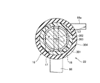
図37は、TFTを示しており、目標着弾位置はチャネル部の中央である。インクジェットにおける目標着弾位置のズレは、目標位置からの距離が半径R=Δ2の円301として表している。ここで、Δ2は、着弾位置ズレ(ステージ誤差+機械加工誤差+吐出角度誤差+熱膨張+…)を示す。つまり、上述した機械誤差やノズル面の状態によって目標としている着弾点からの誤差をΔ2(液滴の滴下位置ずれを考慮した第2の誤差)とすると、図37に示すように、半径R=Δ2の範囲が着弾後の液滴中心が入る領域となる。
【0235】
また、インクジェットで打ったレジスト(液滴)によって加工されるa−Si領域(半導体層16)によって、最低限カバーされなければいけない範囲は、TFTのチャネル部の幅Wと長さLの範囲であるから、インクジェットで吐出した液滴が着弾して円形になったとすれば、図37に示すように、チャネル部中心fを基準にして、丁度半径rの円302となる。ここで、半径rは、TFT中心(チャネル部中心f)からチャネル隅までの距離を示す。すなわち、半径rは、前記チャネル部中心から該チャネル部の最外端までの距離を示す。
【0236】
ここに、先ほどの液量と広がりからの誤差分、つまり液量によって半径が変化する量と、液体が広がって伸びることによる形状の不確定さを見込んで半径を大きく取ったのが半径R=r+Δ1で書かれる円303となる。ここで、Δ1は、液量誤差+広がりバラツキ(広がり誤差)を示す。すなわち、Δ1は、半導体層を構成する液滴の滴下量と該液滴の滴下後の広がりのバラツキとを考慮した第1の誤差を示す。
【0237】
従って、TFTのチャネル部の中央に液滴が着弾した場合、該液滴の液量と領域の不確定さを見込んで最低限、半径R=r+Δ1の円303が書けるような吐出量の液滴を飛ばせば、チャネル部はカバーされることになる。
【0238】
ここに、着弾位置の誤差Δ2を入れた、半径R=r+Δ1+Δ2で書かれる円304がチャネル部中心fを狙って吐出したときの、チャネル部をカバーするための必要半径となる。
【0239】
従って、加工後の半導体層6は、半径Rが、以下の関係式(3)、
R>r+Δ1+Δ2 ・・・・・・・(3)
を満たすように設定されるのが望ましい。
【0240】
図37では、半導体層6の境界を、ソース電極17・ドレイン電極18の上端(TFT部ゲート電極66の端部66a側の端部)からの距離L1で示している。
【0241】
従って、TFTチャネル部中央を狙ってレジストである液滴を着弾させて、半導体層6の加工を行う場合、ソース電極17・ドレイン電極18の上端からの距離L1が、以下の関係式(4)、
L1>Δ1+Δ2 ・・・・・・・(4)
を満たすように該半導体層6の領域境界線が来ることが望ましい。
【0242】
尚、ここでは、TFT部22のチャネル部の幅Wが長さLに比べて長く、Lが大変短いとして、W/2≒rとしている。
【0243】
TFT部ゲート電極66の開放端である端部66aは、半径R=r+Δ1+Δ2の円304が、目標着弾位置からのズレΔ2だけ端部66a方向にずれるので、チャネル部中心fから該端部66aまでの距離をL3とすると、以下の関係式(1)、
L3>r+Δ1+2Δ2 ・・・・・・(1)
を満たす位置に配置することが望ましい。
【0244】
さらに、ソース電極17・ドレイン電極18の端部からの距離をL2とすれば、W/2≒rである場合、以下の関係式(2)
L2>Δ1+2Δ2 ・・・・・・(2)
を満たすように設定することが望ましい。ここでΔ2の前に2をつけたのは誤差に+、−の両方向を考慮した為である。
【0245】
尚、この場合、TFT部ゲート電極66の端部66aの位置を規定する条件は、上記の(1)(2)式の何れであってもよい。
【0246】
図38は、TFT部ゲート電極66の端部66aが図面右方向に曲がった場合を示している。この場合は、ソース電極17・ドレイン電極18の端部からの距離では、TFT部ゲート電極66の端部66aを規定できないので、チャネル部中心fからの距離で該端部66aを規定することができる。この場合は、図38に示すように、TFT部ゲート電極66の端部66aの先端部は、上記(1)式を満たす条件で設定されることが望ましい。
【0247】
ここで、液晶パネルのTFT部22のチャネル寸法は、W=25μm、L=5μmとなっている場合が多い。この寸法におけるrは、r=12.7μm、また、インクジェットにおける目標着弾位置の誤差Δ2は、15μm程度である。また、液量と境界の不確定さからくる変形の誤差Δ1は、5μmであった。
【0248】
従って、この場合の加工後の半導体層6の形状は、12.7+5+15=32.7μmの半径でできる円領域が最低限必要となる。
【0249】
また、図37に示すように、TFT部ゲート電極66の端部66aが真直ぐ伸びる場合、ソース電極17・ドレイン電極18の端部からの該端部66aは、L2>5+2×15=35μmの位置に設定することが望ましい。チャネル部中心fからでは、L3>12.7+5+2×15=47.7μmの条件で該端部66aを設定することが望ましい。なお、ここで、W/2=12.5μm≒r=12.7μmとした。
【0250】
本実施の形態3、4にかかるTFTアレイ基板は、前記実施の形態1、2における各製造工程において、以下に示す工程を追加して製造されるものである。
【0251】
すなわち、前記実施の形態1または2に記載のゲート電極を形成する工程において、ゲート電極13の分岐電極であるTFT部ゲート電極66の、半導体層16の領域から突出している部分(端部66a)の幅を、該半導体層16の領域内の部分の幅よりも小さくなるように形成すれば、本実施の形態3に記載のTFTアレイ基板を製造することができる。
【0252】
また、前記実施の形態1または2に記載のゲート電極を形成する工程において、ゲート電極13の分岐電極であるTFT部ゲート電極66の、半導体層16の領域から突出している部分(端部66a)を、TFT部22のソース電極17またはドレイン電極18の何れか一方に近接して形成すれば、本実施の形態3に記載のTFTアレイ基板を製造することができる。
【0253】
また、前記実施の形態1または2に記載のゲート電極を形成する工程において、ゲート電極13の分岐電極であるTFT部ゲート電極66の、半導体層16の領域から突出している部分(端部66a)を、TFT部22のチャネル部中心fから該チャネル部の最外端までの距離をr、該半導体層16を構成する液滴の滴下量と該液滴の滴下後の広がりのバラツキとを考慮した第1の誤差をΔ1、該液滴の滴下位置ずれを考慮した第2の誤差をΔ2、前記チャネル部中心から前記分岐電極の開放端までの距離をL3としたとき、以下の関係式(1)、
L3>r+Δ1+2Δ2 ・・・・・・・(1)
を満たすように形成すれば、本実施の形態4に記載のTFTアレイ基板を製造することができる。
【0254】
また、前記実施の形態1または2に記載のゲート電極を形成する工程において、ゲート電極13の分岐電極であるTFT部ゲート電極66の、半導体層16の領域から突出している部分(端部66a)を、該半導体層16を構成する液滴の滴下量と該液滴の滴下後の広がりのバラツキとを考慮した第1の誤差をΔ1、該液滴の滴下位置ずれを考慮した第2の誤差をΔ2、TFT部22のソース・ドレイン電極の前記TFT部ゲート電極66の開放端側の端部(端部66a)から該TFT部ゲート電極66の開放端までの距離をL2としたとき、以下の関係式(2)、
L2>Δ1+2Δ2 ・・・・・・・・(2)
を満たすように形成すれば、本実施の形態4に記載のTFTアレイ基板を製造することができる。
【0255】
さらに、前記実施の形態1または2に記載の半導体層16の上にレジスト材料の液滴を滴下して、円形若しくはほぼ円形をしている滴下形状のレジスト層を形成する工程において、前記レジスト材料の液滴の滴下量を、前記TFT部22のチャネル部中心fから該チャネル部の最外端までの距離をr、該レジスト層を構成する液滴の滴下量と該液滴の滴下後の広がりのバラツキとを考慮した第1の誤差をΔ1、該液滴の滴下位置ずれを考慮した第2の誤差をΔ2、前記半導体層の滴下形状の半径をRとしたとき、以下の関係式(3)、
R>r+Δ1+Δ2 ・・・・・・・(3)
を満たすように設定すれば、本実施の形態4に記載のTFTアレイ基板を製造することができる。
【0256】
〔実施の形態5〕
本発明の実施のさらに他の形態を図39ないし図43に基づいて以下に説明する。
【0257】
本実施の形態における液晶表示装置は、図39(a)に示す画素を有している。なお、同図は、液晶表示装置のTFTアレイ基板における1画素の概略構成を示す平面図である。また、同図におけるM−M線矢視断面図を図39(b)に示す。以下、本発明の実施の形態1の場合と実質的に同一機能を有する部材には同一の符号を付記し、その説明は省略する。
【0258】
図39(a)(b)に示すように、TFTアレイ基板121では、ガラス基板12上において、ゲート電極13とソース電極17とがマトリクス状に設けられ、隣り合うゲート電極13の間に補助容量電極14が設けられている。
【0259】
ゲート電極13上には上記ゲート絶縁層15を介してa−Si層を有する半導体層16がほぼ円形に形成され、その上に導電体層122と、ソース電極17およびドレイン電極18が形成されている。
【0260】
導電体層122は、図39(b)に示すように、半導体層16と、TFT部22のソース電極17またはドレイン電極18との間に形成される。そして、その一部には液滴の滴下形状を有し、この液滴の滴下形状の部分において、導電体層122と半導体層16がほぼ同一の形状となっている。
【0261】
ここで、半導体層16は、前記実施の形態1と同様にCVDにより成膜し加工することで形成した。導電体層122は、導電体材料(例えば金属を含む材料)の液滴を滴下して形成した。後に述べるように、半導体層16の形状は導電体層122を形成する途中段階でできる液滴の滴下形状、すなわち導電体成膜層123の形状を反映する。したがって、導電体層122の液滴の滴下形状を有する部分においては、導電体層122と半導体層16はほぼ同じ形状となる。なお、導電体層122の形成に関する詳細は、後述の製造工程において詳細に述べる。
【0262】
本実施の形態においても、前記実施の形態1と同様に、TFTアレイ基板121の製造には、例えば、インクジェット方式により、形成する層の材料を吐出あるいは滴下するパターン形成装置が使用される。例えば、前記実施の形態1の図2に示すようなパターン形成装置が使用される。
【0263】
ここで、前記TFTアレイ基板121の製造方法について説明する。なお、本実施の形態では、前記実施の形態1の図2に示すパターン形成装置を使用してTFTアレイ基板121を製造する場合について説明する。従って、本実施の形態では、前記実施の形態1で説明した図3に示す各製造工程とほぼ同様の製造工程となる。
【0264】
すなわち、TFTアレイ基板121は、図40に示すように、ゲート線前処理工程41、ゲート線塗布形成工程42、ゲート絶縁層成膜・半導体層成膜工程43、半導体層形成工程141、ソース・ドレイン線前処理工程45、ソース・ドレイン線塗布形成工程142、チャネル部加工工程143、保護膜形成工程48、保護膜加工工程49および画素電極形成工程50からなる。このうち、半導体層形成工程141、ソース・ドレイン線塗布形成工程142、およびチャネル部加工工程143以外の工程は、前記実施の形態1と実質的に同等であり、それぞれの説明を省略する。
【0265】
(半導体層形成工程141)
この半導体層形成工程141を図41(a)〜図41(d)で説明する。図41(d)は半導体層形成工程141を経たガラス基板12を示す平面図である。図41(a)〜図41(c)は図41(d)におけるN−N線矢視断面図であり、それぞれ半導体層形成工程141の開始直前状態、途中状態、完了状態における断面図である。
【0266】
図41(a)は、図40に示すゲート絶縁層成膜・半導体層成膜工程43が完了したガラス基板12の状態を示す断面図である。
【0267】
この工程では、図41(b)に示すように、ゲート電極13の本線から分岐したTFT部ゲート電極(分岐電極)66上におけるn+成膜層65の上に、パターン形成装置により導電性材料を滴下させて付着させ、250℃で焼成した。これによって形成された導電体成膜層123を、n+成膜層65、a−Si成膜層64を加工するためのパターンとした。導電性材料の吐出量は例えば10plの液滴1滴とし、TFT部ゲート電極66上における所定の位置にほぼ30μm径の円形のパターンを得ている。
【0268】
なお、焼成温度については、a−Siの形成が約300℃で行われているため、これより低い温度の250℃とした。
【0269】
本実施の形態での導電体成膜層123はMoより構成されるが、これに限らない。Mo以外にも、W、Ag、Cr、Ta、Ti、またはこれらの何れかを主体とする合金材料、またはこれらの何れかを主体としてN、O、C等の非金属元素を含んだ金属材料、またはITO(インジウム錫酸化物)、SnO(錫酸化物)等の金属酸化物によって構成されても良い。
【0270】
また、導電体成膜層123を形成するための導電性材料としては、有機膜をコーティングしたMo微粒子を有機溶媒中に分散させたものを用いたが、この形態に限らず、ペースト材料、あるいは金属化合物として上記金属材料を有機溶媒中に含むもの等を用いることができる。さらに、必要な焼成温度にあわせて、上記微粒子を保護している表面コート層や溶媒の有機材料の乖離温度を制御し、所望の抵抗値および表面状態を得ることが可能である。なお、上記乖離温度とは、上記の表面コート層および溶媒が蒸発する温度のことである。
【0271】
導電体成膜層123を構成する材料としては、次工程のドライエッチング処理に耐えることと、後のチャネル部加工工程143において、ソース電極およびドレイン電極のパターンをマスクにして選択性良くエッチングできることを考慮する必要がある。さらに、半導体層16への拡散が少なく、後のTFT特性に悪影響を与えないことも必要である。
【0272】
次に、ガス(例えばSF6+HCl)を用い、図41(c)に示すように、n+成膜層65およびa−Si成膜層64のドライエッチングを行ってn+層69およびa−Si層68を形成した。
【0273】
上記のように、半導体層形成工程141においては、パターン形成装置によって吐出された導電体成膜層123のパターンがほぼそのまま、n+層69およびa−Si層68からなる半導体層16の形状に反映される。したがって、半導体層16は、導電体成膜層123の材料の液滴がインクジェットヘッド33(図2)からガラス基板12上に滴下されたときのパターンである円形もしくは円形に近い曲線からなるパターンとほぼ同一のパターンに形成される。
【0274】
また、導電体成膜層123の形成は、インクジェットヘッド33からの液滴1滴の滴下にて行っているものの、複数の液滴の滴下より行ってもよい。ただし、液滴を際限なく微小にし、それら微小な液適を緻密に吐出させて導電体成膜層123を形成した場合には、1個の半導体層16を形成するのに長時間を要するばかりか、必要なドット数が増加することによりインクジェットヘッド33の寿命を縮めることになる。従って、複数の液滴の滴下により行なう場合には、製造時間、インクジェットヘッドの寿命等を考慮して、液滴のサイズを設定するのが望ましい。
【0275】
さらに、半導体層形成工程141では、前記実施の形態1の場合と同様、インクジェットヘッド33によって吐出される液滴を受ける面に特別な処理を行う必要が無いことも重要な特徴となっている。
【0276】
従来、半導体層をパターン化するためにはマスクやフォトリソグラフィ工程が必要であった。これに対し、上記の半導体層形成工程141では、インクジェットヘッド33から液滴を滴下して、マスクとなるパターン(レジスト層67(図5(b)に相当))を直接描画しているので、マスクおよびこれを使用するフォトリソグラフィ工程が不要となる。したがって、大幅なコストダウンを実現することができる。
【0277】
(ソース・ドレイン線塗布形成工程142)
図42(a)は、ソース・ドレイン線前処理工程45が完了したガラス基板12の状態を示す平面図である。
【0278】
ソース・ドレイン線塗布形成工程142を図42(b)(c)に示す。図42(b)は、上記配線ガイド71に沿ってソース電極17およびドレイン電極18を形成した状態を示す平面図、図42(c)は図42(b)におけるO−O線矢視断面図である。
【0279】
ソース・ドレイン線塗布形成工程142は、前記実施の形態1の場合とほぼ同様の手順で行われる。ただし、その配線材料としては、後の導電体成膜層123のエッチング処理の条件に合わせ、耐性を有することを考慮しなくてはならない。ここでは、配線材料として、有機膜をコーティングしたAl微粒子を有機溶媒中に分散させたものを用いたが、これに限らない。個々の条件に応じて、Al以外にも、Al−Ti、Al−Nd等のAl合金や、Ag、Ag−Pd、Ag−Cu等のAg合金、ITO(インジウム錫酸化物)、Cu、Cu−Ni等の単体もしくは合金からなる材料の、微粒子もしくはペースト材料、あるいは金属化合物として上記金属材料を有機溶媒中に含むもの等を用いることができる。
【0280】
ここで、必要な焼成の温度は前記実施の形態1の場合と同様に、a−Siの形成が約300℃で行われていることから、200℃としている。本実施の形態においては、後に導電体層122となる導電体成膜層123はMoにより構成されるため、ソース電極17あるいはドレイン電極18を構成するAlが半導体層に拡散することを防止される。従ってこのような焼成処理を経た後でも、Alの半導体層への拡散が小さく、TFTの特性に実用上ほとんど影響を与えないという効果が得られている。
【0281】
(チャネル部加工工程143)
ここでは、TFTのチャネル部72の加工を行う。この処理を図43(a)〜図43(c)に示す。図43(a)〜図43(c)は図42(b)におけるO−O線矢視断面部分に相当する断面図である。
【0282】
まず、図43(a)に示すように、有機溶媒により、あるいはアッシングによりチャネル部72の配線ガイド71を除去した。
【0283】
次に、図43(b)に示すように、導電体成膜層123の一部をソース電極17およびドレイン電極18をマスクとして、選択的に除去し、導電体層122を得た。この処理には重量濃度25%の硝酸を用いたウェットエッチング法を用いた。ここで、導電体成膜層123が除去された部分は、導電体層122の開口部122aとなる。この開口部122aによって、チャネル部72から半導体層16を露出させる。つまり、前記ソース電極17とドレイン電極18とがTFT部22のチャネル部72において、電気的に分離できるように、開口部122aが形成されている。
【0284】
なお、本実施の形態では、ソース電極17およびドレイン電極18の材料はAlであるが、このエッチング条件下においては殆ど侵食されない。このような理由により、導電体成膜層123の一部のみを選択的に除去することが可能である。ただし、導電体成膜層123のエッチング方法、条件は、これに限らない。導電体成膜層123を構成する材料と、ソース電極17およびドレイン電極18を構成する材料、ゲート絶縁層15を構成する材料を考慮し、導電体成膜層123を選択性良くエッチングできる条件であればよい。また、ウェットエッチング法に限らず、ドライエッチング法によっても適切な条件下において可能である。
【0285】
次に、図43(c)に示すように、アッシングもしくはレーザー酸化でn+層69を酸化処理し、不導体化した。
【0286】
本実施の形態では、導電体層122は、導電体成膜層123と同様のMoにより構成され、かつソース電極17あるいはドレイン電極18と半導体層16の間に位置する。そのため、導電体層122はソース電極17あるいはドレイン電極18を構成する材料のAlが半導体層16へ拡散することを実質上防止する拡散防止層として機能する。
【0287】
従って、本実施の形態では、このチャネル部加工工程143に続いて行なわれる基板加熱を含む工程を経ても、半導体層16へのAlの拡散が実質上防止され、TFTの特性に実用上ほとんど影響を与えないというメリットが得られる。基板加熱とは、より具体的には、例えば保護膜形成工程48におけるSiO2膜の成膜、感光性アクリル樹脂層20の形成、画素電極形成工程50におけるITO微粒子材料の焼成等である。
【0288】
なお、ソース・ドレイン塗布形成工程142において説明したように、導電体層122を、例えばMoのような半導体層16へのAlの拡散を防ぐ材料によって構成しておけば、その前段階である導電体成膜層123にも同様な効果をもたせることができる。従って、ソース・ドレイン塗布形成工程142において加わる基板の200℃の焼成においても、半導体層16へのAlの拡散を防ぐことができ、TFTの特性に実用上ほとんど影響を与えないというメリットが得られる。
【0289】
また、ソース電極17およびドレイン電極18を構成する材料はAlに限らず、Alを主体とする金属材料、例えば、Al合金でも良い。この場合には、Moにより構成された導電体層122は、Al合金の成分元素であるAlのみ、またはAl以外の合金の成分元素のみ、またはこれらの両方が半導体層16へ拡散することを実質上防ぐ機能をもつことになる。
【0290】
ソース電極17およびドレイン電極18を構成する材料として、Alのような拡散しやすい材料を用いる場合、従来のように拡散防止層を半導体層16の形成後に別途形成する方法、例えばソース電極17あるいはドレイン電極18を、ガラス基板12側に拡散防止層と、低電気抵抗層の2層から構成する方法では生産性が大きく下がる。
【0291】
これに対して、本実施の形態のように、導電体層122、あるいは導電体成膜層123を拡散防止層として機能させれば、拡散防止層を別途設ける必要がなくなるので、生産性を大幅に向上させることができる。
【0292】
特に本実施の形態のように、ソース電極17あるいはドレイン電極18をインクジェット方式のような塗布方式によるときには効果が大きい。塗布方式の場合、2層目の塗布を行うためには1層目の塗布材料が十分に固まっていなくてはならず、2度の塗布の間に加熱等の処理が必要となる。この場合、一度塗布装置で処理した基板を焼成装置に搬入した後、再度塗布装置に搬入することになる等、非常に煩雑な工程となるため、生産性が大幅に下がる。一方、本実施の形態においては、従来の方法ではソース電極17あるいはドレイン電極18を構成する材料の成分元素が半導体層16へ拡散することが懸念される場合でも、ソース電極17あるいはドレイン電極18は、そのまま1度の塗布により形成できるため、生産性を落とすことが無い。
【0293】
本実施の形態ではこのように、導電体層122となる途中段階の導電体成膜層123に、半導体層16を形成するパターンマスクとなる役割と、半導体層16への拡散防止層となる役割の2つの役割をもたせることができる。加えて、導電体層122自体にも拡散防止効果をもたせることができる。従って、生産性を落とすことなく、ソース電極17あるいはドレイン電極18として、半導体層16への拡散が生じ易い金属材料を用いることができるという大きな効果がある。
【0294】
上記のように、本TFTアレイ基板121の製造方法では、インクジェット方式によるパターン形成装置を用いない従来の製造方法と比較すると、マスク枚数を従来の5枚から3枚に減らすことができ、フォトリソグラフィ工程や、真空成膜装置を大幅に削減することができる。これにより、設備投資額も大幅に削減することができる。さらに、ソース電極17あるいはドレイン電極18を構成する材料として、半導体層16への拡散が起きやすい材料を、生産性を落とすことなく用いることができるメリットがある。
【0295】
なお、本実施の形態5で説明した事項、例えば図39に示すTFTアレイ基板や図40に示す製造方法において、前記実施の形態1〜4でそれぞれ説明した事項を適宜組み合わせることも可能である。但し、説明に矛盾が生じない組み合わせに限る。
【0296】
本実施の形態5のTFTアレイ基板に対して、例えば、薄膜トランジスタ部22のTFT部ゲート電極66は、ゲート電極13における本線からの分岐電極であり、前記分岐電極における開放端が前記半導体層16の領域から突出するようにしてもよい。
【0297】
また、前記分岐電極の、前記半導体層の領域から突出している部分の幅が、該半導体層の領域内の部分の幅よりも小さくてもよい。
【0298】
前記半導体層16の上には、ソース電極17とドレイン電極18とが形成され、かつこれら両電極間にチャネル部72が形成され、前記分岐電極の、前記半導体層16の領域から突出している部分は、前記ソース電極17またはドレイン電極18の何れか一方に近接して形成されていてもよい。
【0299】
また、前記半導体層16の上には、ソース電極17とドレイン電極18とが形成され、かつこれら両電極間にチャネル部72が形成され、前記分岐電極の、前記半導体層72の領域から突出している部分は、前記チャネル部72中心から該チャネル部72の最外端までの距離をr、該半導体層16を構成する液滴の滴下量と該液滴の滴下後の広がりのバラツキとを考慮した第1の誤差をΔ1、該液滴の滴下位置ずれを考慮した第2の誤差をΔ2、前記チャネル部中心から前記分岐電極の開放端までの距離をL3としたとき、以下の関係式(1)、
L3>r+Δ1+2Δ2 ・・・・・・・(1)
を満たすように形成されていてもよい。
【0300】
また、前記半導体層16の上には、ソース電極17とドレイン電極18とが形成され、かつこれら両電極間にチャネル部72が形成され、前記分岐電極の、前記半導体層16の領域から突出している部分は、該半導体層16を構成する液滴の滴下量と該液滴の滴下後の広がりのバラツキとを考慮した第1の誤差をΔ1、該液滴の滴下位置ずれを考慮した第2の誤差をΔ2、前記ソース・ドレイン電極の前記分岐電極の開放端側の端部から該分岐電極の開放端までの距離をL2としたとき、以下の関係式(2)、
L2>Δ1+2Δ2 ・・・・・・・・(2)
を満たすように形成されていてもよい。
【0301】
また、前記半導体層16の上には、ソース電極17とドレイン電極18とが形成され、かつこれら両電極間にチャネル部72が形成され、前記ソース電極17およびドレイン電極18における前記チャネル部72側の端部が、それらの全幅にわたって前記半導体層16の領域内に位置していてもよい。
【0302】
さらに、少なくとも前記半導体層16の上層若しくは下層の何れか一方の前記半導体層16の位置に対応する位置に、液滴の滴下形状の遮光膜が形成されていてもよい。
【0303】
また、前記半導体層16の上には、ソース電極17とドレイン電極18とが形成され、かつこれら両電極間にチャネル部72が形成され、前記半導体層16は、前記チャネル部72中心から該チャネル部72の最外端までの距離をr、該半導体層16を構成する液滴の滴下量と該液滴の滴下後の広がりのバラツキとを考慮した第1の誤差をΔ1、該液滴の滴下位置ずれを考慮した第2の誤差をΔ2、前記半導体層の滴下形状の半径をRとしたとき、前記導電性材料の液滴の滴下量を、以下の関係式(3)、
R>r+Δ1+Δ2 ・・・・・・・(3)
を満たすように設定することによって形成されていてもよい。
【0304】
また、本実施の形態5のTFTアレイ基板の製造方法に対して、例えば、薄膜トランジスタ部22のTFT部ゲート電極66は、ゲート電極13における本線からの分岐電極であり、前記分岐電極における開放端が半導体層16の領域から突出するようにしてもよい。
【0305】
また、前記分岐電極は、前記分岐電極における開放端が半導体層16の領域から突出するように、液滴の滴下精度に基づいた長さに設定してもよい。
【0306】
また、前記分岐電極の、半導体層16の領域から突出している部分の幅を、該半導体層の領域内の部分の幅よりも小さくなるように形成してもよい。
【0307】
また、前記分岐電極の、半導体層16の領域から突出している部分を、前記薄膜トランジスタ部のソース電極またはドレイン電極の何れか一方に近接して形成してもよい。
【0308】
さらに、ゲート電極13を形成する工程において、前記分岐電極の、半導体層16の領域から突出している部分を、前記薄膜トランジスタ部のチャネル部72中心からチャネル部72の最外端までの距離をr、半導体層16を構成する液滴の滴下量と該液滴の滴下後の広がりのバラツキとを考慮した第1の誤差をΔ1、該液滴の滴下位置ずれを考慮した第2の誤差をΔ2、チャネル部72部中心から前記分岐電極の開放端までの距離をL3としたとき、以下の関係式(1)、
L3>r+Δ1+2Δ2 ・・・・・・・(1)
を満たすように形成してもよい。
【0309】
さらに、ゲート電極13を形成する工程において、前記分岐電極の、半導体層16の領域から突出している部分を、半導体層16を構成する液滴の滴下量と該液滴の滴下後の広がりのバラツキとを考慮した第1の誤差をΔ1、該液滴の滴下位置ずれを考慮した第2の誤差をΔ2、前記薄膜トランジスタ部のソース電極17・ドレイン電極18の前記分岐電極の開放端側の端部から該分岐電極の開放端までの距離をL2としたとき、以下の関係式(2)、
L2>Δ1+2Δ2 ・・・・・・・・(2)
を満たすように形成してもよい。
【0310】
また、第1の領域および第2の領域を前記液滴の流出を阻止する凸状のガイドにより形成してもよい。
【0311】
また、第1の領域および第2の領域の形成を前記液滴に対する親液領域と撥液領域とを形成してもよい。
【0312】
以上の本実施の形態5は、前記各実施の形態と適宜組み合わせることが可能であり、また、組み合わせたときの作用効果も、前記各実施の形態における作用効果と同じである。
【0313】
また、本実施の形態5に開示したTFTアレイ基板は、液晶表示装置に好適に用いられる。しかしながら、これに限定されるものではなく、有機ELパネルや無機ELパネル等の表示装置、指紋センサー、X線撮像装置などに代表される二次元画像入力装置等、TFTアレイ基板を使用する各種電子装置において用いることが可能である。このことは、前記実施の形態1〜4において開示したTFTアレイ基板においても同様であり、適用可能な装置としては、液晶表示装置に限らず、上述した各種装置に適用可能である。
【0314】
さらに、本実施の形態5に開示したTFTアレイ基板の製造方法は、液晶表示装置の製造方法に好適に用いられる。しかしながら、これに限定されるものではなく、上述した有機ELパネルや無機ELパネル等の表示装置の製造方法、指紋センサー、X線撮像装置などに代表される二次元画像入力装置の製造方法等、TFTアレイ基板を使用する各種電子装置の製造方法において用いることが可能である。このことは、前記実施の形態1〜4において開示したTFTアレイ基板の製造方法においても同様であり、適用可能な製造方法としては、液晶表示装置の製造方法に限らず、上述した各種装置に適用可能である。
【0315】
本発明は上述した各実施形態に限定されるものではなく、請求項に示した範囲で種々の変更が可能であり、異なる実施形態にそれぞれ開示された技術的手段を適宜組み合わせて得られる実施形態についても本発明の技術的範囲に含まれる。
【0316】
【発明の効果】
以上のように、本発明のTFTアレイ基板は、半導体層が液滴の滴下形状をなしている構成である。
【0317】
これにより、TFTアレイ基板の製造において、半導体層を形成するためのマスクが不要となり、必要なマスク数が減少する結果、製造工数を削減することができる。また、マスクを使用したフォトリソグラフィ工程が減少するので、フォトリソグラフィ工程のための設備費の削減が可能であるのに加えて、廃棄される材料の量が減少する。これにより、製造時間の短縮およびコストダウンが可能となる。
【0318】
上記のTFTアレイ基板は、前記薄膜トランジスタ部のゲート電極が、ゲート電極における本線からの分岐電極であり、前記分岐電極における開放端が前記半導体層の領域から突出している構成としてもよい。
【0319】
上記の構成によれば、薄膜トランジスタ部における、ゲート電極の分岐電極は、半導体層の領域から開放端が突出した形状となっているので、分岐電極からの電界の作用により、ソース・ドレイン電極間のリーク電流を適切に抑制することができる。
【0320】
また、本発明のTFTアレイ基板は、前記分岐電極の、前記半導体層の領域から突出している部分の幅を、該半導体層の領域内の部分の幅よりも小さくなるように形成した構成としてもよい。
【0321】
上記の構成によれば、画素部にかかる分岐電極の開放端が該画素部に占める割合が小さくなり、開口率の低下を抑制できる。
【0322】
また、本発明のTFTアレイ基板は、前記半導体層の上には、ソース電極とドレイン電極とが形成され、かつこれら両電極間にチャネル部が形成され、前記分岐電極の、前記半導体層の領域から突出している部分は、前記ソース電極またはドレイン電極の何れか一方に近接して形成された構成としてもよい。
【0323】
上記の構成によれば、分岐電極の、前記半導体層の領域から突出している部分を、ソース電極またはドレイン電極の何れか一方に近接して形成することで、TFTアレイ基板の画素部内で、開口率を低下させることなく、該分岐電極の開放端の突出部分を延ばして形成することができる。
【0324】
これにより、半導体層の領域から分岐電極の開放端を確実に突出させた状態にすることができるので、ソース・ドレイン電極間のリーク電流を確実に抑制することができる。
【0325】
また、前記分岐電極の、前記半導体層の領域から突出している部分は、以下のようにして規定することが考えられる。
【0326】
すなわち、本発明のTFTアレイ基板は、前記半導体層の上には、ソース電極とドレイン電極とが形成され、かつこれら両電極間にチャネル部が形成され、前記分岐電極の、前記半導体層の領域から突出している部分は、前記チャネル部中心から該チャネル部の最外端までの距離をr、該半導体層を構成する液滴の滴下量と該液滴の滴下後の広がりのバラツキとを考慮した第1の誤差をΔ1、該液滴の滴下位置ずれを考慮した第2の誤差をΔ2、前記チャネル部中心から前記分岐電極の開放端までの距離をL3としたとき、以下の関係式(1)、
L3>r+Δ1+2Δ2 ・・・・・・・(1)
を満たすように形成した構成としてもよい。
【0327】
また、本発明のTFTアレイ基板は、前記半導体層の上には、ソース電極とドレイン電極とが形成され、かつこれら両電極間にチャネル部が形成され、前記分岐電極の、前記半導体層の領域から突出している部分は、該半導体層を構成する液滴の滴下量と該液滴の滴下後の広がりのバラツキとを考慮した第1の誤差をΔ1、該液滴の滴下位置ずれを考慮した第2の誤差をΔ2、前記ソース・ドレイン電極の前記分岐電極の開放端側の端部から該分岐電極の開放端までの距離をL2としたとき、以下の関係式(2)、
L2>Δ1+2Δ2 ・・・・・・・・(2)
を満たすように形成した構成としてもよい。
【0328】
上記のTFTアレイ基板は、前記半導体層の上にソース電極とドレイン電極とが形成され、かつこれら両電極間にチャネル部が形成され、前記ソース電極およびドレイン電極における前記チャネル部側の端部が、それらの全幅にわたって前記半導体層の領域内に位置している構成としてもよい。
【0329】
上記の構成によれば、各画素のソース電極において十分なON電流を得ることができるので、各画素の充電状態が不均一となって画像斑が生じる事態を防止することができる。
【0330】
上記のTFTアレイ基板は、少なくとも前記半導体層の上層若しくは下層の何れか一方の前記半導体層の位置に対応する位置に、液滴の滴下形状の遮光膜が形成されている構成としてもよい。
【0331】
上記の構成によれば、遮光膜は必要に応じて形成されるものの、遮光膜が必要な場合には、前記半導体層の形成の場合と同様、マスクを使用することなく、遮光膜を例えばインクジェット方式を利用した遮光膜材料の液滴の例えば1滴の滴下により容易に形成することが可能となる。これにより、TFTアレイ基板の製造工程において、マスクや大幅な材料追加を伴うことなく形成することが可能なため、製造工数の低減およびコストダウンが可能となる。
【0332】
また、本発明のTFTアレイ基板は、前記半導体層の上には、ソース電極とドレイン電極とが形成され、かつこれら両電極間にチャネル部が形成され、前記半導体層は、前記チャネル部中心から該チャネル部の最外端までの距離をr、該半導体層を構成する液滴の滴下量と該液滴の滴下後の広がりのバラツキとを考慮した第1の誤差をΔ1、該液滴の滴下位置ずれを考慮した第2の誤差をΔ2、前記半導体層の滴下形状の半径をRとしたとき、前記レジスト材料の液滴の滴下量、あるいは、前記半導体材料の液滴の滴下量を、以下の関係式(3)、
R>r+Δ1+Δ2 ・・・・・・・(3)
を満たすように設定することによって形成した構成としてもよい。
【0333】
上記の構成によれば、薄膜トランジスタ部のチャネル部に半導体層を確実に形成することができるので、該薄膜トランジスタ部の特性を低下させないようにできる。
【0334】
本発明の液晶表示装置は、上記のTFTアレイ基板を備えている構成である。したがって、液晶表示装置の製造工程において、必要なマスク数が減少する結果、製造時間の短縮およびコストダウンが可能となる。
【0335】
本発明のTFTアレイ基板の製造方法は、基板上にゲート電極を形成する工程と、前記ゲート電極の上にゲート絶縁層を形成する工程と、前記ゲート絶縁層の上に半導体膜を成膜する工程と、前記半導体膜の上にレジスト材料の液滴を滴下して、液滴の滴下形状のレジスト層を形成する工程と、前記レジスト層の形状に前記半導体膜を加工して薄膜トランジスタ部の半導体層を形成した後、前記レジスト層を除去する工程とを備えている構成である。
【0336】
これにより、成膜された半導体膜の上にレジスト材料の液滴を滴下して、液滴の滴下形状(通常はほぼ円形)のレジスト層を形成し、このレジスト層をマスクとして半導体層を形成することができる。
【0337】
したがって、半導体層を形成するためのマスクが不要となり、必要なマスク数が減少する結果、製造工数を削減することができる。また、マスクを使用したフォトリソグラフィ工程が減少するので、フォトリソグラフィ工程のための設備費の削減が可能であるのに加えて、廃棄される材料の量が減少する。これにより、製造時間の短縮およびコストダウンが可能となる。
【0338】
本発明のTFTアレイ基板の製造方法は、基板上にゲート電極を形成する工程と、前記ゲート電極の上にゲート絶縁層を形成する工程と、前記分岐電極上における前記ゲート絶縁層の上に半導体材料の液滴を滴下し、薄膜トランジスタ部の半導体層として、前記液滴の滴下形状の半導体層を形成する工程とを備えている構成である。
【0339】
これにより、分岐電極上におけるゲート絶縁層の上に半導体材料の液滴を滴下することのみにより、液滴の滴下形状(通常はほぼ円形)の半導体層を形成することができる。
【0340】
したがって、半導体層を形成するためのマスクが不要となり、必要なマスク数が減少する結果、製造工数を削減することができる。また、マスクを使用したフォトリソグラフィ工程が減少するので、フォトリソグラフィ工程のための設備費の削減が可能であるのに加えて、廃棄される材料の量が減少する。これにより、製造時間の短縮およびコストダウン並びに材料の有効利用が可能となる。
【0341】
上記のTFTアレイ基板の製造方法は、ゲート電極を形成する前記工程では本線とこの本線からの分岐電極を有するゲート電極形成し、前記分岐電極における開放端が前記半導体層の領域から突出している構成としてもよい。
【0342】
上記の構成によれば、薄膜トランジスタ部における、ゲート電極の分岐電極は、半導体層の領域から開放端が突出した形状となっているので、分岐電極からの電界の作用により、ソース・ドレイン電極間のリーク電流を適切に抑制することができる。
【0343】
上記のTFTアレイ基板の製造方法は、前記分岐電極が、前記分岐電極における開放端が前記半導体層の領域から突出するように、液滴の滴下精度に基づいた長さに設定されている構成としてもよい。
【0344】
上記の構成によれば、レジスト材料の液滴あるいは半導体材料の液滴を、最終的に形成される半導体層の領域から分岐電極の開放端が確実に突出する位置に滴下させることが可能となる。この結果、ソース・ドレイン電極間のリーク電流を適切に抑制可能となる。
【0345】
本発明のTFTアレイ基板の製造方法は、前記分岐電極の、前記半導体層の領域から突出している部分の幅を、該半導体層の領域内の部分の幅よりも小さくなるように設定する構成としてもよい。
【0346】
上記の構成によれば、画素部にかかる分岐電極の開放端が該画素部に占める割合を小さくできるので、開口率の低下を抑制できる。
【0347】
本発明のTFTアレイ基板の製造方法は、前記分岐電極の、前記半導体層の領域から突出している部分を、前記薄膜トランジスタ部のソース電極またはドレイン電極の何れか一方に近接して形成する構成としてもよい。
【0348】
上記の構成によれば、分岐電極の、前記半導体層の領域から突出している部分を、ソース電極またはドレイン電極の何れか一方に近接して形成することで、TFTアレイ基板の画素部内で、開口率を低下させることなく、該分岐電極の開放端の突出部分を延ばして形成することができる。
【0349】
これにより、半導体層の領域から分岐電極の開放端を確実に突出させた状態にすることができるので、ソース・ドレイン電極間のリーク電流を確実に抑制することができる。
【0350】
本発明のTFTアレイ基板の製造方法は、前記ゲート電極を形成する工程において、前記分岐電極の、前記半導体層の領域から突出している部分を、前記薄膜トランジスタ部のチャネル部中心から該チャネル部の最外端までの距離をr、該半導体層を構成する液滴の滴下量と該液滴の滴下後の広がりのバラツキとを考慮した第1の誤差をΔ1、該液滴の滴下位置ずれを考慮した第2の誤差をΔ2、前記チャネル部中心から前記分岐電極の開放端までの距離をL3としたとき、以下の関係式(1)、
L3>r+Δ1+2Δ2 ・・・・・・・(1)
を満たすように形成する構成としてもよい。
【0351】
また、前記ゲート電極を形成する工程において、前記分岐電極の、前記半導体層の領域から突出している部分を、該半導体層を構成する液滴の滴下量と該液滴の滴下後の広がりのバラツキとを考慮した第1の誤差をΔ1、該液滴の滴下位置ずれを考慮した第2の誤差をΔ2、前記薄膜トランジスタ部のソース・ドレイン電極の前記分岐電極の開放端側の端部から該分岐電極の開放端までの距離をL2としたとき、以下の関係式(2)、
L2>Δ1+2Δ2 ・・・・・・・・(2)
を満たすように形成する構成としてもよい。
【0352】
何れの構成であっても、半導体層の領域から分岐電極の開放端を確実に突出させた状態にすることができるので、ソース・ドレイン電極間のリーク電流を確実に抑制することができる。
【0353】
また、本発明のTFTアレイ基板の製造方法は、前記半導体膜の上にレジスト材料の液滴を滴下して、円形若しくはほぼ円形をしている滴下形状のレジスト層を形成する工程において、前記レジスト材料の液滴の滴下量を、前記薄膜トランジスタ部のチャネル部中心から該チャネル部の最外端までの距離をr、該半導体層を構成する液滴の滴下量と該液滴の滴下後の広がりのバラツキとを考慮した第1の誤差をΔ1、該液滴の滴下位置ずれを考慮した第2の誤差をΔ2、前記半導体層の滴下形状の半径をRとしたとき、以下の関係式(3)、
R>r+Δ1+Δ2 ・・・・・・・(3)
を満たすように設定する構成としてもよい。
【0354】
上記の構成によれば、薄膜トランジスタ部のチャネル部に半導体層を確実に形成することができるので、該薄膜トランジスタ部の特性を低下させないようにできる。
【0355】
本発明のTFTアレイ基板の製造方法は、基板上にゲート電極を形成する工程と、前記ゲート電極の上にゲート絶縁層を形成する工程と、前記ゲート絶縁層の上に薄膜トランジスタ部の半導体層を形成する工程と、前記半導体層の形成工程を経た基板に対し、電極材料の液滴の滴下によりソース電極を形成するための第1の領域、および電極材料の液滴の滴下により少なくとも画素電極を形成するための第2の領域を形成する前処理工程と、前記前処理工程を経た基板に対し、第1の領域と第2の領域とに電極材料の液滴を滴下して、ソース電極、ドレイン電極および画素電極を形成する電極形成工程とを備えている構成である。
【0356】
これにより、電極形成工程に対する1つの前処理工程において、電極材料の液滴の滴下によりソース電極を形成するための第1の領域と電極材料の液滴の滴下により少なくとも画素電極を形成するための第2の領域とを形成するので、第1の領域と第2の領域とを別々の工程にて形成する場合と比較して、製造工数を削減し、コストダウンが可能となる。
【0357】
本発明の液晶表示装置の製造方法は、上記の何れかのTFTアレイ基板の製造方法を含んでいる構成である。したがって、少なくとも、液晶表示装置の製造工数を削減し、コストダウンが可能となる。
【0358】
本発明のTFTアレイ基板は、基板にゲート電極が形成され、このゲート電極の上にゲート絶縁層を介して半導体層と、導電体層とが形成された薄膜トランジスタ部を備えているTFTアレイ基板であって、前記導電体層が、前記半導体層と、前記薄膜トランジスタ部のソース電極またはドレイン電極と接して形成されるとともに、その一部に液滴の滴下形状を有し、この液滴の滴下形状の部分において、前記導電体層と半導体層とがほぼ同一の形状を有することを特徴としている。
【0359】
それゆえ、成膜された半導体膜の上に導電性材料の液滴を滴下して、液滴の滴下形状(通常はほぼ円形)の導電体成膜層を形成し、この導電体成膜層をさらに加工して、導電体層を得ることができる。導電体成膜層は、半導体層を形成するためのマスクとして用いられるが、レジスト材料の場合とは異なって除去する工程が不要である。ここでは、導電性材料の液滴の半導体膜上への滴下方法としては、例えば、インクジェット方式を利用することが考えられるが、これに限定されるものではなく、薄膜トランジスタの半導体層程度の大きさの液滴形状を形成可能な方式であれば、何れの方式であっても使用することができる。
【0360】
このようなTFTアレイ基板の構成によれば、半導体層を形成するためのマスクが不要となり、必要なマスク枚数が減少すること、さらに導電体成膜層を除去しないことからレジストを用いたときのような剥離工程が不要であるため、製造工数と設備費を大きく削減することができる。それに加えて、使用する現像液、剥離液などの薬液の使用量を削減し、レジスト材料等の廃棄される材料の量も削減することができる。これらにより、製造時間の短縮およびコストダウンが可能となる。
【0361】
また、前記導電体層は、Mo、W、Ag、Cr、Ta、Ti、またはこれらの何れかを主体とする金属材料、またはインジウム錫酸化物から構成されることを特徴としてもよい。
【0362】
つまり、上記の構成によれば、導電体層はソース電極あるいはドレイン電極と半導体層の間に位置するため、導電体層はソース電極あるいはドレイン電極を構成する材料の成分元素が半導体層へ拡散することを実質上防止する拡散防止層として機能する。また、導電体層になる前段階の導電体成膜層であっても、同様に拡散防止層として機能する。このように、拡散を実質上防止することで、加熱処理を経た後でも、半導体層への拡散が小さく、TFTの特性に実用上ほとんど影響を与えない。
【0363】
このような構成は、近年ソース電極あるいはドレイン電極を構成する材料としてAl、Cuなどの半導体層に拡散しやすい材料が用いられるという状況に対応し得るものである。このように、本発明の上記の構成は、製造工程をほとんど増やさずに、ソース電極あるいはドレイン電極を構成する材料の選択の幅を広げるという効果がある。
【0364】
このような本発明の構成では、従来のように拡散防止層を半導体層の形成後に形成する方法、例えばソース電極あるいはドレイン電極を、ガラス基板側から拡散防止層と低電気抵抗層の2層から構成する方法に比べて製造工程が削減される。従って、TFTアレイ基板の生産性を向上させる効果が得られる。
【0365】
特に、前記ソース電極とドレイン電極が、AlまたはAlを主体とする金属材料からなることは製造プロセス上有利である。
【0366】
AlまたはAlを主体とする金属材料の性質としては、硝酸等の酸化力のある酸には、侵されにくい性質がある。加えて、導電体成膜層をAg、Mo、W、あるいはそれらを主体とする合金など、硝酸等の酸化力のある酸に可溶な金属材料で構成しておく。すると、硝酸等の酸化力のある酸を用いて、導電体成膜層のみを選択性良くウェットエッチング処理を行うことができるという製造プロセス上の効果を得ることができる。
【0367】
さらに、ソース電極とドレイン電極が、AlまたはAlを主体とする金属材料からなるので低電気抵抗であり、近年のTFTアレイ基板の大型化にも対応している。
【0368】
また、本発明の液晶表示装置は、上記のTFTアレイ基板を備えていることを特徴としている。したがって、液晶表示装置の製造工程において、TFTアレイ基板の製造工数の削減した結果、製造時間の短縮およびコストダウンが可能となる。
【0369】
本発明のTFTアレイ基板の製造方法は、基板上にゲート電極を形成する工程と、前記ゲート電極の上にゲート絶縁層を形成する工程と、前記ゲート絶縁層の上に半導体膜を成膜する工程と、前記半導体膜の上に導電性材料の液滴を滴下して、液滴の滴下形状の導電体成膜層を形成する工程と、前記導電体成膜層の形状に前記半導体膜を加工して薄膜トランジスタ部の半導体層を形成する工程とを備えている構成である。
【0370】
それゆえ、成膜された半導体膜の上に導電性材料の液滴を滴下して、液滴の滴下形状(通常はほぼ円形)の導電体成膜層を形成し、この導電体成膜層をマスクとして半導体層を形成することができる。この導電体成膜層はレジスト材料の場合とは異なり、除去する工程を行わなくて良い。
【0371】
このようなTFTアレイ基板の製造方法によれば、半導体層を形成するためのマスクが不要となり、必要なマスク枚数が減少することにより、製造工数を削減することができる。また、マスクを使用したフォトリソグラフィ工程が減少するので、フォトリソグラフィ工程のための設備費の削減が可能であるのに加えて、現像液、剥離液などの薬液の使用量、レジスト材料等の廃棄される材料の量が減少する。これにより、製造時間の短縮およびコストダウンが可能となる。
【0372】
さらに、前記導電体成膜層を加工して導電体層を形成する工程を備え、前記導電体層をMo、W、Ag、Cr、Ta、Ti、またはこれらの何れかを主体とする金属材料、またはインジウム錫酸化物から構成することを特徴とする製造方法であってよい。
【0373】
このようにすれば、製造工程をほとんど増やさずに、ソース電極あるいはドレイン電極を構成する材料の選択の幅を広げることができる。つまり、導電体層となる途中段階の導電体成膜層に、半導体層を形成するパターンマスクとなる役割と、半導体層への拡散防止層となる役割の2つの役割をもたせることができる。
加えて、導電体層自体にも拡散防止効果をもたせることができる。従って、ソース電極あるいはドレイン電極を構成する材料に低電気抵抗のAl、Cuが使えるなど、材料の選択の幅を広げることができる効果がある。
【0374】
また、前記ソース電極とドレイン電極を、AlまたはAlを主体とする金属材料で形成することを特徴としてもよい。
【0375】
これに加えて、導電体成膜層をAg、Mo、W、あるいはそれらを主体とする合金など、硝酸等の酸化力のある酸に可溶な金属材料で構成しておくと、硝酸等の酸化力のある酸を用いて、導電体成膜層のみを選択性良くウェットエッチング処理を行うことができるという製造プロセス上の効果を得ることができる。
【0376】
従って、TFTアレイ基板の製造工数を減らすこと等ができるので、TFTアレイ基板の生産性の向上を図ることができる。
【0377】
本発明の液晶表示装置の製造方法は、上記の何れかのTFTアレイ基板の製造方法を含んでいることを特徴としている。したがって、少なくとも、液晶表示装置の製造工数を削減できる。
【図面の簡単な説明】
【図1】図1(a)は本発明の実施の一形態の液晶表示装置におけるTFTアレイ基板の1画素の概略構成を示す平面図、図1(b)は図1(a)におけるA−A線矢視断面図である。
【図2】本発明の実施の一形態における液晶表示装置の製造に使用するインクジェット方式のパターン形成装置を示す概略の斜視図である。
【図3】図1に示したTFTアレイ基板の製造工程を示すフローチャートである。
【図4】図4(a)は図3に示したゲート前処理工程を説明するTFTアレイ基板の平面図、図4(b)は同ゲート線塗布形成工程を説明するTFTアレイ基板の平面図、図4(c)は図4(b)におけるB−B線矢視断面図である。
【図5】図5(a)〜図5(c)は図4(b)におけるB−B線矢視断面に相当する部分の断面図であって、図5(a)は図3に示したゲート絶縁層成膜・半導体層成膜工程を示すもの、図5(b)は図3に示した半導体層形成工程におけるa−Si成膜層およびn+成膜層の成膜処理を示すもの、図5(c)は同工程におけるa−Si成膜層およびn+成膜層のエッチング処理を示すもの、図5(d)は同工程におけるレジストの除去処理を示すものであって、図5(e)におけるC−C線矢視断面、図5(e)は半導体層形成工程を経たTFTアレイ基板の平面図である。
【図6】図6(a)は図3に示したソース・ドレイン線前処理工程を説明するTFTアレイ基板の平面図、図6(b)は同ソース・ドレイン線塗布形成工程を説明するTFTアレイ基板の平面図、図6(c)は図6(b)におけるD−D線矢視断面図である。
【図7】図1(a)に示したTFTアレイ基板におけるTFT部を示す平面図である。
【図8】図8(a)(b)は図6(b)におけるD−D線矢視断面部分に相当する断面図であって、図8(a)は図3に示したチャネル部加工工程における配線ガイドの除去処理を示すもの、図8(b)は同工程におけn+層の酸化処理を示すものである。
【図9】図9(a)は図3に示した保護膜形成工程および保護膜加工工程を説明するTFTアレイ基板の平面図、図9(b)は図9(a)におけるE−E線矢視断面図である。
【図10】図10(a)は図3に示した画素電極形成工程を説明するTFTアレイ基板の平面図、図10(b)は図10(a)におけるF−F線矢視断面図である。
【図11】図1(a)に示したTFT部でのリーク電流の発生メカニズムの説明図であって、図11(a)はTFT部ゲート電極が半導体パターンを突抜けている場合におけるTFT部の平面図、図11(b)は図11(a)におけるG−G線矢視断面図である。
【図12】図12(a)は、上記リーク電流の発生メカニズムの説明図であって、図11(a)の構成に対し、TFT部ゲート電極が半導体パターンを突抜けていない場合におけるTFT部の平面図、図12(b)は図12(a)におけるH−H線矢視断面図である。
【図13】図1(a)に示したTFT部においてTFT部ゲート電極に対してa−Si層が偏って存在した場合を示すTFT部の示す平面図である。
【図14】図14(a)は、下部の遮光膜に加えて上部の遮光膜を有するTFTアレイ基板の製造方法を示すものであって、チャネル部のエッチング完了状態を示すTFTアレイ基板の縦断面図、図14(b)は、上部の遮光膜の形成工程を示すTFTアレイ基板の縦断面図、図14(c)は、図14(d)におけるM−M線矢視断面図、図14(d)は、画素電極の形成完了状態を示すTFTアレイ基板の平面図である。
【図15】図15(a)は、本発明の実施の他の形態の液晶表示装置におけるTFTアレイ基板の1画素の概略構成を示す平面図、図15(b)は図15(a)におけるI−I線矢視断面図である。
【図16】図15に示したTFTアレイ基板の製造工程を示すフローチャートである。
【図17】図16に示したソース・ドレイン・画素電極前処理工程を説明するTFTアレイ基板の平面図図である。
【図18】図18(a)は図16に示したソース線塗布形成工程を説明するTFTアレイ基板の平面図、図18(b)は図18(a)におけるJ−J線矢視断面図である。
【図19】図19(a)は図16に示したドレイン・画素電極塗布形成工程を説明するTFTアレイ基板の平面図、図19(b)は図19(a)におけるK−K線矢視断面図である。
【図20】図20(a)(b)は図19(a)におけるK−K線矢視断面部分に相当する断面図であって、図20(a)は図16に示したチャネル部加工工程における配線ガイドの除去処理を示すもの、図20(b)は同工程におけるn+層の酸化処理を示すものである。
【図21】図19(a)におけるK−K線矢視断面部分に相当する断面図であって、図16に示した保護膜形成工程を説明するものである。
【図22】図22(a)は、本実施のさらに他の形態のTFTアレイ基板における、半導体層形成前の状態を示す断面図、図22(b)は、半導体層を形成したTFTアレイ基板を示すものであって、図22(c)におけるL−L線矢視断面図、図22(c)は半導体層を形成したTFTアレイ基板を示す平面図である。
【図23】本発明の実施のさらに他の形態の液晶表示装置におけるTFTアレイ基板の1画素の概略構成を示す平面図である。
【図24】図2に示したパターン形成装置からの液滴の滴下により形成される滴下形状の一例を示すものであって、滴下形状がほぼ円形である場合を示す説明図である。
【図25】図25(a)は、図24に示した滴下形状の他の例を示すものであって、滴下形状が円形に近いものの円形から変形した形状である場合、図25(b)は凹み部を有する形状である場合、図25(c)は凸部を一部に含んだような形状である場合を示す説明図である。
【図26】図26(a)は、図24に示した滴下形状の他の例を示すものであって、滴下形状が2滴の滴下によって変形楕円形状となった場合、図26(b)は滴下形状が3滴の滴下によって形成された場合を示す説明図である。
【図27】図27(a)は、本願発明が意図しない状態であって、液滴を無限小にし、これら液滴を敷き詰めて滴下した状態を示す説明図、図27(b)は27(a)の状態により形成される滴下形状を示す説明図である。
【図28】従来の液晶表示装置におけるTFTアレイ基板の製造工程を示すフローチャートである。
【図29】本発明のTFTアレイ基板のTFT特性を示すグラフである。
【図30】TFTアレイ基板のTFT部の拡大図であり、ゲート電極の開放端が半導体層から突き出ていない状態を示す図である。
【図31】TFTアレイ基板のTFT部の拡大図であり、ゲート電極の開放端が半導体層から突き出ている状態の一例を示す図である。
【図32】TFTアレイ基板のTFT部の拡大図であり、ゲート電極の開放端が半導体層から突き出ている状態の一例を示す図である。
【図33】本発明の実施の他の形態の液晶表示装置におけるTFTアレイ基板の1画素の概略構成を示す平面図である。
【図34】本発明の実施の他の形態の液晶表示装置におけるTFTアレイ基板の1画素の概略構成を示す平面図である。
【図35】図33に示すTFTアレイ基板の1画素の要部拡大図である。
【図36】図34に示すTFTアレイ基板の1画素の要部拡大図である。
【図37】TFT部におけるゲート電極開放端と半導体層境界領域との関係を規定するための説明図である。
【図38】TFT部におけるゲート電極開放端と半導体層境界領域との関係を規定するための他の説明図である。
【図39】図39(a)は本発明の実施の一形態の液晶表示装置におけるTFTアレイ基板の1画素の概略構成を示す平面図、図39(b)は図39(a)におけるM−M線矢視断面図である。
【図40】図40は、図39(a)(b)に示したTFTアレイ基板の製造工程を示すフローチャートである。
【図41】図41(d)は半導体層形成工程を経たガラス基板12を示す平面図であり、図41(a)〜図41(c)は図41(d)におけるN−N線矢視断面図であり、それぞれ半導体層形成工程の開始直前状態、途中状態、完了状態における断面図である。
【図42】図42(a)は図40に示したソース・ドレイン線前処理工程を説明するTFTアレイ基板の平面図、図42(b)は同ソース・ドレイン線塗布形成工程を説明するTFTアレイ基板の平面図、図42(c)は図42(b)におけるO−O線矢視断面図である。
【図43】図43(a)〜(c)は図42(b)におけるO−O線矢視断面部分に相当する断面図であって、図43(a)は図40に示したチャネル部加工工程における配線ガイドの除去処理を示すもの、図43(b)は、同工程における導電体成膜層の部分的エッチング処理を示すもの、図43(c)は同工程におけn+層の部分的酸化処理を示すものである。
【符号の説明】
11 TFTアレイ基板
12 ガラス基板
13 ゲート電極
14 補助容量電極
15 ゲート絶縁層
16 半導体層
17 ソース電極
18 ドレイン電極
19 保護膜
20 感光性アクリル樹脂層
21 画素電極
22 TFT部
23 補助容量部
24 コンタクトホール
33 インクジェットヘッド
61 ゲート線形成領域
62 遮光膜
63 補助容量電極形成領域
64 a−Si成膜層
65 n+成膜層
66 TFT部ゲート電極(分岐電極)
66a 端部
67 レジスト層
68 a−Si層
69 n+層
71,84,85 配線ガイド
72 チャネル部
73 ソース・ドレイン形成領域
81 TFTアレイ基板
82 ドレイン・画素電極
83 保護膜
86 ソース形成領域
87 ドレイン・画素電極形成領域
121 TFTアレイ基板
122 導電体層
122a 開口部
123 導電体成膜層
201 TFTアレイ基板
202 突出電極
211 TFTアレイ基板
212 突出電極[0001]
BACKGROUND OF THE INVENTION
The present invention relates to a TFT array substrate, a liquid crystal display device, a method for manufacturing a TFT array substrate, and a method for manufacturing a liquid crystal display device.
[0002]
[Prior art]
Conventionally, in a liquid crystal display device provided with a TFT (Thin Film Transistor), the TFT array substrate is manufactured by a series of steps shown in FIG. That is, the conventional TFT array substrate manufacturing process includes gate line formation, gate line formation, gate insulating layer formation / semiconductor layer formation, semiconductor layer formation, source / drain line formation, source / drain line formation, channel Each process (101 to 111) includes partial processing, protective film formation, protective film processing, pixel electrode film formation, and pixel electrode formation.
[0003]
In the five processes, the gate
[0004]
On the other hand, in recent years, a technique for forming a wiring by an ink jet method without using photolithography has been proposed. In this technique, for example, as disclosed in Patent Document 1 (Japanese Patent Laid-Open No. 11-204529), an affinity region and a non-affinity region for a wiring forming material are formed on a substrate on which a wiring is formed, and the affinity region is formed. Wiring is formed by dropping droplets of wiring material on the ink jet method.
[0005]
Similarly, in Patent Document 2 (Japanese Patent Application Laid-Open No. 2000-353594), in the wiring formation technique based on the inkjet method, banks are formed on both sides of the wiring formation region in order to suppress the protrusion of the wiring material from the wiring formation region. It is disclosed that the upper part of the bank is made non-lyophilic and the wiring formation region is made lyophilic.
[0006]
Non-Patent Document 1 (SID 01 DIGEST, pages 40-43, 6.1: Invited Paper: All-Polymer Thin Film Transistors Fabricated by High-Resolution Ink-jet Printing (author Takeo Kawase et al.)) A technique for forming TFTs using organic materials as materials is disclosed.
[0007]
[Patent Document 1]
Japanese Patent Laid-Open No. 11-204529 (published July 30, 1999)
[0008]
[Patent Document 2]
JP 2000-353594 A (published on December 19, 2000)
[0009]
[Non-Patent Document 1]
SID 01 DIGEST, pages 40-43, 6.1: Invited Paper: All-Polymer Thin Film Transistors Fabricated by High-Resolution Ink-jet Printing (author Takeo Kawase et al.), 2001
[0010]
[Problems to be solved by the invention]
In the conventional TFT array substrate manufacturing method using photolithography, as described above, the gate
[0011]
In addition, the amount of resist and wiring materials used has increased with the increase in size of substrates.
On the other hand, in processing such as formation of wiring, most materials such as resist are removed and discarded by etching and peeling processes, and are not effectively used. For this reason, disposal processing and disposal costs are also greatly increased due to the increase in the size of the substrate, and the environmental load is increased due to the waste. As described above, the manufacturing method of the TFT array substrate mainly including a large number of photolithography results in an increase in manufacturing steps and an increase in cost.
[0012]
On the other hand, for example, if the inkjet method disclosed in the above-mentioned conventional document is used, the number of masks required in the manufacturing process of the TFT array substrate can be reduced. Thus, for example, there has been a demand for the development of a technique that can reduce the number of manufacturing steps and reduce the cost by using an inkjet method.
[0013]
[Means for Solving the Problems]
In order to solve the above problems, the TFT array substrate of the present invention includes a thin film transistor portion in which a gate electrode is formed on the substrate and a semiconductor layer is formed on the gate electrode via a gate insulating layer. The TFT array substrate is characterized in that the semiconductor layer has a droplet dropping shape.
[0014]
According to the above configuration, since the semiconductor layer has a droplet dropping shape (for example, a shape that is almost circular or overlapped while shifting a circle), the semiconductor layer is a liquid of a semiconductor material that uses an inkjet method. For example, it can be formed by dropping one drop. Alternatively, for example, a droplet of a resist material, for example, is dropped on the semiconductor film by using an inkjet method to form a resist layer, and the semiconductor film is processed using the resist layer as a mask. It becomes possible to form.
Alternatively, it is possible to form a conductor film-forming layer using droplets of a conductive material instead of a resist material by using an inkjet method, and to form a semiconductor layer in the same manner using this as a mask.
[0015]
According to such a method, in manufacturing the TFT array substrate, a mask for forming a semiconductor layer is not necessary, and the number of necessary masks is reduced. As a result, the number of manufacturing steps can be reduced. Further, since the photolithography process using the mask is reduced, the equipment cost for the photolithography process can be reduced, and the amount of material to be discarded is reduced. Thereby, shortening of manufacturing time and cost reduction are possible.
[0016]
Note that the dropping of the semiconductor material, the resist material, and the conductive material is not limited to the above-described inkjet method, and any method that can directly form the semiconductor layer, the resist layer, and the conductive film formation layer by dropping the material droplets. It can be used.
[0017]
The TFT array substrate may have a configuration in which the gate electrode of the thin film transistor portion is a branch electrode from the main line of the gate electrode, and an open end of the branch electrode protrudes from the region of the semiconductor layer.
[0018]
According to the above configuration, since the branch electrode of the gate electrode in the thin film transistor portion has a shape in which the open end protrudes from the region of the semiconductor layer, the electric field from the branch electrode causes the gap between the source and drain electrodes. Leakage current can be appropriately suppressed.
[0019]
As described above, when the branch electrode of the gate electrode is formed so that the open end protrudes from the region of the semiconductor layer, when the pixel portion of the TFT array substrate is transparent like the transmissive liquid crystal display device, the protruding open There is a possibility that the end is covered with the pixel portion and the aperture ratio is lowered. In the case of a TFT array substrate applied to a reflective liquid crystal display device, it is not necessary to consider the problem of the aperture ratio as described above, so that the degree of freedom in designing the branch electrode is increased.
[0020]
Therefore, the TFT array substrate of the present invention may be configured such that the width of the portion of the branch electrode protruding from the semiconductor layer region is smaller than the width of the portion in the semiconductor layer region. Good.
[0021]
According to said structure, the ratio for which the open end of the branch electrode concerning a pixel part accounts to this pixel part becomes small, and it can suppress the fall of an aperture ratio.
[0022]
In the TFT array substrate of the present invention, a source electrode and a drain electrode are formed on the semiconductor layer, and a channel portion is formed between the two electrodes. The region of the semiconductor layer of the branch electrode The portion projecting from may be configured to be formed close to either the source electrode or the drain electrode.
[0023]
According to the above configuration, the portion of the branch electrode that protrudes from the region of the semiconductor layer is formed close to one of the source electrode and the drain electrode, thereby opening the pixel portion of the TFT array substrate. The protruding portion of the open end of the branch electrode can be extended without reducing the rate.
[0024]
Thereby, since the open end of the branch electrode can be reliably projected from the region of the semiconductor layer, the leakage current between the source and drain electrodes can be reliably suppressed.
[0025]
As a result, the characteristics of the thin film transistor can be improved.
[0026]
Further, it can be considered that the portion of the branch electrode protruding from the region of the semiconductor layer is defined as follows.
[0027]
That is, in the TFT array substrate of the present invention, a source electrode and a drain electrode are formed on the semiconductor layer, and a channel portion is formed between both electrodes, and the region of the semiconductor layer of the branch electrode is formed. For the portion protruding from the channel portion, the distance from the center of the channel portion to the outermost end of the channel portion is r, and the amount of droplets forming the semiconductor layer and the dispersion of the spread after the droplets are dropped are considered. Assuming that the first error is Δ1, the second error considering the droplet dropping position deviation is Δ2, and the distance from the center of the channel portion to the open end of the branch electrode is L3, the following relational expression ( 1),
L3> r + Δ1 + 2Δ2 (1)
It is good also as a structure formed so that it may satisfy | fill.
[0028]
In the TFT array substrate of the present invention, a source electrode and a drain electrode are formed on the semiconductor layer, and a channel portion is formed between the two electrodes. The region of the semiconductor layer of the branch electrode The portion protruding from the first portion takes into account the first error taking into account the drop amount of the droplets constituting the semiconductor layer and the spread of the droplets after dropping, and the drop position deviation of the droplets is taken into account When the second error is Δ2, and the distance from the open end side end of the branch electrode of the source / drain electrode to the open end of the branch electrode is L2, the following relational expression (2):
L2> Δ1 + 2Δ2 (2)
It is good also as a structure formed so that it may satisfy | fill.
[0029]
In the TFT array substrate, a source electrode and a drain electrode are formed on the semiconductor layer, and a channel portion is formed between the two electrodes. An end portion on the channel portion side of the source electrode and the drain electrode is formed on the TFT array substrate. The semiconductor layer may be located in the semiconductor layer region over the entire width thereof.
[0030]
According to the above configuration, since a sufficient ON current can be obtained at the source electrode of each pixel, it is possible to prevent the occurrence of image spots due to non-uniform charging state of each pixel.
[0031]
The TFT array substrate may have a configuration in which a light-blocking film having a droplet drop shape is formed at a position corresponding to the position of at least one of the upper and lower layers of the semiconductor layer.
[0032]
According to the above configuration, the light shielding film is formed as necessary. However, when the light shielding film is necessary, the light shielding film can be formed by, for example, inkjet without using a mask, as in the case of forming the semiconductor layer. It can be easily formed by, for example, dropping one droplet of the light shielding film material using the method. Thereby, in the manufacturing process of the TFT array substrate, it can be formed without adding a mask or significant material, so that the number of manufacturing steps can be reduced and the cost can be reduced.
[0033]
In the TFT array substrate of the present invention, a source electrode and a drain electrode are formed on the semiconductor layer, and a channel portion is formed between these electrodes. The semiconductor layer is formed from the center of the channel portion. The distance to the outermost end of the channel portion is r, the first error taking into account the drop amount of the droplets constituting the semiconductor layer and the spread of the droplets after the droplets are dropped is Δ1, The second error considering the drop position deviation is Δ2, semiconductor Layered Dripping shape radius The When R is The amount of droplets of the resist material, or the amount of droplets of the semiconductor material, The following relational expression (3),
R> r + Δ1 + Δ2 (3)
To meet By setting It is good also as the formed structure.
[0034]
According to the above configuration, since the semiconductor layer can be reliably formed in the channel portion of the thin film transistor portion, the characteristics of the thin film transistor portion can be prevented from being deteriorated.
[0035]
The liquid crystal display device of the present invention is characterized by comprising the above TFT array substrate. Therefore, in the manufacturing process of the liquid crystal display device, the number of necessary masks is reduced, so that the manufacturing time can be shortened and the cost can be reduced.
[0036]
The manufacturing method of the TFT array substrate of the present invention includes a step of forming a gate electrode on the substrate, a step of forming a gate insulating layer on the gate electrode, and a semiconductor film on the gate insulating layer. A step of dropping a droplet of a resist material on the semiconductor film to form a resist layer having a droplet dropping shape; and processing the semiconductor film into the shape of the resist layer to form a semiconductor of a thin film transistor portion And a step of removing the resist layer after forming the layer.
[0037]
According to the above configuration, a droplet of a resist material is dropped on the deposited semiconductor film to form a resist layer having a droplet dropping shape (usually substantially circular), and this resist layer is used as a mask. A semiconductor layer can be formed.
[0038]
According to such a method for manufacturing a TFT array substrate, a mask for forming a semiconductor layer is not required, and the number of necessary masks is reduced. As a result, the number of manufacturing steps can be reduced. Further, since the photolithography process using the mask is reduced, the equipment cost for the photolithography process can be reduced, and the amount of material to be discarded is reduced. Thereby, shortening of manufacturing time and cost reduction are possible.
[0039]
The dropping of the resist material is not limited to the ink jet method, and any method can be used as long as the resist layer can be directly formed by dropping the material droplets.
[0040]
The TFT array substrate manufacturing method of the present invention includes a step of forming a gate electrode on a substrate, a step of forming a gate insulating layer on the gate electrode, and a droplet of a semiconductor material on the gate insulating layer. And a step of forming a droplet-shaped semiconductor layer as a semiconductor layer of the thin film transistor portion.
[0041]
According to the above configuration, a semiconductor layer having a droplet dropping shape (usually substantially circular) can be formed only by dropping a droplet of a semiconductor material on the gate insulating layer on the branch electrode.
[0042]
According to such a method for manufacturing a TFT array substrate, a mask for forming a semiconductor layer is not required, and the number of necessary masks is reduced. As a result, the number of manufacturing steps can be reduced. Further, since the photolithography process using the mask is reduced, the equipment cost for the photolithography process can be reduced, and the amount of material to be discarded is reduced. Thereby, shortening of manufacturing time, cost reduction, and effective utilization of materials become possible.
[0043]
Note that the dropping of the semiconductor material is not limited to the inkjet method, and any method can be used as long as the semiconductor layer can be directly formed by dropping a droplet of the material.
[0044]
In the TFT array substrate manufacturing method, in the step of forming the gate electrode, a gate electrode having a main line and a branch electrode from the main line is formed, and an open end of the branch electrode protrudes from the region of the semiconductor layer. It is good also as a structure.
[0045]
According to the above configuration, since the branch electrode of the gate electrode in the thin film transistor portion has a shape in which the open end protrudes from the region of the semiconductor layer, the electric field from the branch electrode causes the gap between the source and drain electrodes. Leakage current can be appropriately suppressed.
[0046]
The manufacturing method of the TFT array substrate is configured such that the branch electrode is set to a length based on droplet dropping accuracy such that an open end of the branch electrode protrudes from the region of the semiconductor layer. Also good.
[0047]
According to the above configuration, it is possible to drop a droplet of a resist material or a droplet of a semiconductor material at a position where the open end of the branch electrode reliably protrudes from the region of the semiconductor layer to be finally formed. . As a result, the leakage current between the source and drain electrodes can be appropriately suppressed.
[0048]
The manufacturing method of the TFT array substrate of the present invention is configured such that the width of the portion of the branch electrode protruding from the region of the semiconductor layer is set to be smaller than the width of the portion in the region of the semiconductor layer. Also good.
[0049]
According to said structure, since the ratio for which the open end of the branch electrode concerning a pixel part accounts to this pixel part can be made small, the fall of an aperture ratio can be suppressed.
[0050]
The manufacturing method of the TFT array substrate of the present invention may be configured such that a portion of the branch electrode protruding from the region of the semiconductor layer is formed close to either the source electrode or the drain electrode of the thin film transistor portion. Good.
[0051]
According to the above configuration, the portion of the branch electrode that protrudes from the region of the semiconductor layer is formed close to one of the source electrode and the drain electrode, thereby opening the pixel portion of the TFT array substrate. The protruding portion of the open end of the branch electrode can be extended without reducing the rate.
[0052]
Thereby, since the open end of the branch electrode can be reliably projected from the region of the semiconductor layer, the leakage current between the source and drain electrodes can be reliably suppressed.
[0053]
In the method of manufacturing a TFT array substrate according to the present invention, in the step of forming the gate electrode, a portion of the branch electrode that protrudes from the region of the semiconductor layer is moved from the center of the channel portion of the thin film transistor portion to the outermost portion of the channel portion. The distance to the outer edge is r, the first error taking into account the drop amount of the droplets constituting the semiconductor layer and the spread of the droplets after the drop is dropped is Δ1, and the drop position deviation of the droplets is taken into account When the second error is Δ2, and the distance from the channel portion center to the open end of the branch electrode is L3, the following relational expression (1),
L3> r + Δ1 + 2Δ2 (1)
It is good also as a structure formed so that it may satisfy | fill.
[0054]
Further, in the step of forming the gate electrode, the portion of the branch electrode that protrudes from the region of the semiconductor layer has a variation in the amount of droplets that constitute the semiconductor layer and the spread after the droplets are dropped. The first error in consideration of the above is Δ1, the second error in consideration of the droplet dropping position deviation is Δ2, and the branch from the end of the open end side of the branch electrode of the source / drain electrode of the thin film transistor portion When the distance to the open end of the electrode is L2, the following relational expression (2),
L2> Δ1 + 2Δ2 (2)
It is good also as a structure formed so that it may satisfy | fill.
[0055]
In any configuration, the open end of the branch electrode can be reliably projected from the region of the semiconductor layer, so that the leakage current between the source and drain electrodes can be reliably suppressed.
[0056]
Further, in the manufacturing method of the TFT array substrate of the present invention, a droplet of a resist material is dropped on the semiconductor film, It is circular or almost circular In the step of forming the drop-shaped resist layer, the resist Drop volume of material droplet The distance from the center of the channel portion of the thin film transistor portion to the outermost end of the channel portion is r, and the amount of droplets constituting the semiconductor layer and the spread after the droplets are dropped are considered. The error of 1 is Δ1, the second error considering the drop position deviation of the droplet is Δ2, semiconductor Layered Dripping shape radius The When R is assumed, the following relational expression (3),
R> r + Δ1 + Δ2 (3)
To meet Setting It is good also as composition to do.
[0057]
According to the above configuration, since the semiconductor layer can be reliably formed in the channel portion of the thin film transistor portion, the characteristics of the thin film transistor portion can be prevented from being deteriorated.
[0058]
The manufacturing method of the TFT array substrate of the present invention includes a step of forming a gate electrode on the substrate, a step of forming a gate insulating layer on the gate electrode, and a semiconductor layer of a thin film transistor portion on the gate insulating layer. A first region for forming a source electrode by dropping an electrode material droplet, and at least a pixel electrode by dropping an electrode material droplet on the substrate that has undergone the forming step and the semiconductor layer forming step. A pretreatment step for forming a second region to be formed, and a droplet of an electrode material is dropped on the first region and the second region with respect to the substrate that has undergone the pretreatment step; And an electrode forming step for forming a drain electrode and a pixel electrode.
[0059]
According to the above configuration, in one pre-processing step for the electrode forming step, at least the pixel electrode is formed by dropping the first region for forming the source electrode by dropping the electrode material droplet and the droplet of the electrode material. Since the second region to be formed is formed, the number of manufacturing steps can be reduced and the cost can be reduced as compared with the case where the first region and the second region are formed in separate steps. .
[0060]
In the above TFT array substrate manufacturing method, the first region and the second region may be formed by a convex guide that prevents the liquid droplet from flowing out. Or it is good also as a structure formed by the lyophilic area | region and liquid repellent area | region with respect to the said droplet.
[0061]
A method for manufacturing a liquid crystal display device according to the present invention includes any one of the above-described methods for manufacturing a TFT array substrate. Therefore, at least the number of manufacturing steps for the liquid crystal display device can be reduced.
[0062]
The TFT array substrate of the present invention is a TFT array substrate having a thin film transistor portion in which a gate electrode is formed on the substrate and a semiconductor layer and a conductor layer are formed on the gate electrode via a gate insulating layer. The conductor layer is formed in contact with the semiconductor layer and the source electrode or drain electrode of the thin film transistor portion, and has a droplet dropping shape at a part thereof, and the droplet dropping shape In this part, the conductor layer and the semiconductor layer have substantially the same shape.
[0063]
According to the above configuration, a conductive material droplet is dropped on the deposited semiconductor film to form a conductive film forming layer having a droplet dropping shape (usually substantially circular). The body film-forming layer can be further processed to obtain a conductor layer. The conductor film-forming layer is used as a mask for forming a semiconductor layer, but does not require a step of removing unlike a resist material. Here, as a method for dropping a droplet of a conductive material onto a semiconductor film, for example, an inkjet method may be used, but the method is not limited to this, and the size is approximately the same as that of a semiconductor layer of a thin film transistor. Any method can be used as long as it can form the droplet shape.
[0064]
Such a TFT array substrate configuration eliminates the need for a mask for forming a semiconductor layer, reduces the number of necessary masks, and does not remove the conductor film-forming layer. Since such a peeling process is unnecessary, the number of manufacturing steps can be reduced. In addition, since the number of photolithographic processes using masks is reduced, the equipment costs for the photolithographic processes can be reduced. In addition, the amount of developer and stripper used can be reduced, and resist materials and other materials can be discarded. The amount of material that is played is reduced. Thereby, shortening of manufacturing time and cost reduction are possible.
[0065]
The conductor layer may be made of Mo, W, Ag, Cr, Ta, Ti, a metal material mainly composed of any of these, or indium tin oxide.
[0066]
Here, the metal material mainly composed of any one of Mo, W, Ag, Cr, Ta, and Ti may be an alloy material, or may contain a nonmetallic element such as N, O, or C. The material of the conductor layer shown here has a small diffusion into its own semiconductor layer, and is used as a diffusion preventing layer.
[0067]
In other words, according to the above configuration, since the conductor layer is located between the source or drain electrode and the semiconductor layer, the constituent elements of the material constituting the source or drain electrode diffuse into the semiconductor layer. It functions as a diffusion prevention layer that substantially prevents this. In addition, the conductor film-forming layer at the previous stage that becomes the conductor layer also functions as a diffusion preventing layer. Here, substantially preventing the diffusion means that the diffusion into the semiconductor layer is small even after the heat treatment, and practically does not affect the characteristics of the TFT.
[0068]
According to the above configuration, the conventional method of forming the diffusion prevention layer after the formation of the semiconductor layer, for example, the source electrode or the drain electrode is constituted by two layers of the diffusion prevention layer and the low electrical resistance layer from the glass substrate side. Compared with the method, the manufacturing process is greatly reduced.
[0069]
In recent years, the TFT array substrate has been increased in size so that the source electrode or the drain electrode is required to have low electrical resistance, and the materials constituting them are Al, Cu, which easily diffuse into the semiconductor layer when directly in contact with the semiconductor layer. Such materials are increasingly used. The configuration of the present invention as described above can cope with this situation. As described above, the above-described configuration of the present invention expands the range of selection of the material constituting the source electrode or the drain electrode without increasing the number of manufacturing steps.
[0070]
In the TFT array substrate having the above-described configuration according to the present invention, when the conductor layer is configured in this manner, it serves as a pattern mask for forming the semiconductor layer on the conductor film-forming layer in the middle of the conductor layer. And, it can have two roles as a role of preventing diffusion to the semiconductor layer. In addition, the conductor layer itself can have a diffusion preventing effect. Therefore, when a material such as Al or Cu that easily diffuses into the semiconductor layer is used for the source electrode or the like, the manufacturing process is greatly reduced, and the productivity of the TFT array substrate can be improved.
[0071]
In particular, it is desirable that the source electrode and the drain electrode are made of Al or a metal material mainly composed of Al.
[0072]
Here, the metal material mainly composed of Al may be an Al alloy material such as Al—Ti or Al—Nd, or may be a metal material mainly composed of Al and containing a nonmetallic element such as N, O, or C. .
[0073]
The conductor film-forming layer in the present invention is partially etched using the pattern of the source electrode and the drain electrode and separated into a conductor layer. This is a process necessary for electrically separating the source electrode and the drain electrode of the TFT.
[0074]
According to said structure, it is possible to wet-etch the said conductor film-forming layer, hardly damaging a source electrode or a drain electrode.
[0075]
For this purpose, it is utilized that Al or a metal material mainly composed of Al is hardly attacked by an acid having an oxidizing power such as nitric acid.
[0076]
At this time, in addition, the conductor film-forming layer is made of a metal material that is soluble in an acid having an oxidizing power such as nitric acid, such as Ag, Mo, W, or an alloy mainly composed of them. Then, the conductive film can be wet-etched with high selectivity by an acid having oxidizing power such as nitric acid, and the conductor is hardly affected by Al or a source electrode made of a metal material mainly composed of Al. A layer can be obtained.
[0077]
Furthermore, in the TFT array substrate having the above-described configuration of the present invention, the source electrode is made of Al or a metal material mainly composed of Al, so it has low electrical resistance, and can cope with the recent increase in size of the TFT array substrate. is doing.
[0078]
The TFT array substrate configured as described above according to the present invention has both low electrical resistance and suitability for a manufacturing process in which a conductive film-forming layer for forming a conductive layer can be etched with high selectivity. It is very useful.
[0079]
The dropping of the conductive material for forming the conductive film formation layer is not limited to the ink jet method, and any method that can directly form the conductive film formation layer by dropping the material droplets can be used. is there.
[0080]
In addition, a liquid crystal display device of the present invention includes the above-described TFT array substrate. Therefore, in the manufacturing process of the liquid crystal display device, the number of manufacturing steps of the TFT array substrate is reduced, so that the manufacturing time can be shortened and the cost can be reduced.
[0081]
As a manufacturing method of such a TFT array substrate, there are the following methods.
[0082]
The manufacturing method of the TFT array substrate of the present invention includes a step of forming a gate electrode on the substrate, a step of forming a gate insulating layer on the gate electrode, and a semiconductor film on the gate insulating layer. A step of dropping a droplet of a conductive material on the semiconductor film to form a droplet-shaped conductor film-forming layer; and forming the semiconductor film in the shape of the conductor film-forming layer. And processing to form a semiconductor layer of the thin film transistor portion.
[0083]
According to the above configuration, a conductive material droplet is dropped on the deposited semiconductor film to form a conductive film forming layer having a droplet dropping shape (usually substantially circular). The semiconductor layer can be formed using the body film-forming layer as a mask. Unlike the resist material, this conductor film-forming layer does not need to be removed.
[0084]
According to such a method for manufacturing a TFT array substrate, a mask for forming a semiconductor layer becomes unnecessary, and the number of necessary masks can be reduced, thereby reducing the number of manufacturing steps. In addition, since the number of photolithographic processes using masks is reduced, the equipment costs for the photolithographic processes can be reduced, and the amount of chemicals such as developer and stripper used, and the disposal of resist materials, etc. The amount of material that is played is reduced. Thereby, shortening of manufacturing time and cost reduction are possible.
[0085]
The dropping of the conductive material is not limited to the ink jet method, and any method that can directly form the conductive film formation layer by dropping the material droplets can be used.
[0086]
Further, the conductor layer may be made of Mo, W, Ag, Cr, Ta, Ti, a metal material mainly composed of any of these, or indium tin oxide.
[0087]
The source electrode and the drain electrode may be formed of Al or a metal material mainly composed of Al.
[0088]
A method for manufacturing a liquid crystal display device according to the present invention includes any one of the above-described methods for manufacturing a TFT array substrate. Therefore, at least the number of manufacturing steps for the liquid crystal display device can be reduced.
[0089]
In addition, the TFT array substrate of the present invention is not limited to a liquid crystal display device but can be applied to other electronic devices. Here, as other electronic devices, for example, display devices such as organic EL panels and inorganic EL panels, two-dimensional image input devices represented by fingerprint sensors, X-ray imaging devices, etc. There are electronic devices.
[0090]
DETAILED DESCRIPTION OF THE INVENTION
[Embodiment 1]
An embodiment of the present invention will be described below with reference to FIGS.
[0091]
A liquid crystal display device according to an embodiment of the present invention includes the pixel shown in FIG. The figure is a plan view showing a schematic configuration of one pixel in the TFT array substrate of the liquid crystal display device. Moreover, the sectional view on the AA line in the same figure is shown in FIG.1 (b).
[0092]
As shown in FIGS. 1A and 1B, in the
[0093]
As shown in FIG. 1B, the
[0094]
A
[0095]
In this embodiment, the
[0096]
The pattern forming apparatus performs various controls such as an
[0097]
The
[0098]
Next, a method for manufacturing the
[0099]
In this embodiment, as shown in FIG. 3, the
[0100]
(Gate line pretreatment step 41)
In the gate
[0101]
This processing is roughly as follows. First, on the substrate (glass substrate 12), the liquid wiring material is given a property of being easily wetted or repelled, and a hydrophilic region (lyophilic region) as the gate
[0102]
In the former, a hydrophilic / hydrophobic treatment with a photocatalyst using titanium oxide is representative. In the latter, a resist material is used and guide formation is performed by photolithography. Furthermore, in order to impart hydrophilicity to the guide or the substrate surface, they are made CF in plasma. Four , O 2 A process of exposing to gas may be performed. The resist is removed after the wiring is formed.
[0103]
Here, the photocatalytic treatment using titanium oxide was performed as follows. That is, the
[0104]
Here, when it is expected that very strong light is applied to the
[0105]
In order to simplify the description, in the process explanatory diagrams of FIG. 4 and subsequent figures, in the upper gate electrode, an electrode branched from the gate electrode and forming a TFT is omitted.
[0106]
(Gate line coating formation process 42)
This gate line
[0107]
In this process, a wiring material is applied to the gate
[0108]
Since the wiring material discharged from the
[0109]
The reason why the baking temperature is set to 350 ° C. is that processing heat of about 300 ° C. is applied in the semiconductor
[0110]
Further, as the wiring material, in addition to Ag, use may be made of a simple substance such as Ag—Pd, Ag—Au, Ag—Cu, Cu, Cu—Ni or the like containing fine particles of an alloy material or a paste material in an organic solvent. Is possible. Furthermore, for the wiring material, it is possible to obtain the desired resistance value and surface state by controlling the dissociation temperature of the surface coating layer protecting the fine particles and the organic material of the solvent in accordance with the required firing temperature. is there. The dissociation temperature is a temperature at which the surface coat layer and the solvent evaporate.
[0111]
(Gate insulation layer deposition / semiconductor layer deposition step 43)
FIG. 5A shows this gate insulating layer deposition / semiconductor
In this process, three layers of the
[0112]
(Semiconductor layer forming step 44)
This semiconductor
[0113]
In this step, as shown in FIG. 5B, a resist material is formed on the n +
[0114]
As a material for the resist
[0115]
Next, gas (eg SF 6 As shown in FIG. 5C, the n +
[0116]
As described above, in the semiconductor
[0117]
The resist
[0118]
An important point in each process using the
[0119]
Further, the semiconductor
[0120]
In addition, the substrate surface that has been subjected to baking, treatment in gas (dry etching), or the like is likely to have a short molecule attached thereto, which is a case where a semiconductor other than a-Si, for example, an organic semiconductor is used. However, the ejected liquid droplets often exist with a certain large contact angle.
[0121]
Conventionally, in order to pattern a semiconductor layer, a mask or a photolithography process has been required. On the other hand, in the semiconductor
[0122]
(Source / drain line pretreatment step 45)
This source / drain
[0123]
In this step, the
[0124]
The SiNx surface (the upper surface of the gate insulating layer 15) is subjected to a hydrophilic treatment with oxygen plasma so that the wiring material applied by the pattern forming apparatus is well adapted to the surface to be the base surface. CF in the plasma Four Water repellent treatment may be performed by flowing gas.
[0125]
Further, in place of the formation of the
[0126]
(Source / drain line coating formation process 46)
This source / drain line
[0127]
In the source / drain line
[0128]
Note that although the same wiring material as that used for the
[0129]
The basic structure of the TFT is almost completed by the
[0130]
Here, what is important in the
[0131]
(Channel part processing step 47)
Here, the
[0132]
(Protective
9A and 9B show a state where the protective
[0133]
Here, first, on the
[0134]
Next, this SiO 2 An acrylic resist material to be the photosensitive
[0135]
In the formation of the pattern, a part for removing the resist layer after development and a part for removing about half in thickness were formed on the mask. The latter is an area for halftone exposure having a transmittance of about 50%. That is, the resist layer is completely removed from the portion where the
[0136]
(Pixel electrode forming step 50)
On the pixel electrode formation pattern of the photosensitive
[0137]
Conventionally, using a mask for each of terminal processing and ITO processing Photolithography Although the process has been performed, by performing halftone exposure using a photosensitive acrylic resin, a single mask can also be used for these processes, thereby reducing the number of masks and reducing the cost. .
[0138]
Here, the generation mechanism of the leakage current shown in the source / drain line
[0139]
FIG. 11A is a plan view of the TFT portion when the TFT
[0140]
In the TFTs of FIGS. 11A and 11B (TFT portion gate electrode protruding state) and FIGS. 12A and 12B (TFT portion gate electrode not protruding state), a voltage of −4 V, for example, is applied to the
[0141]
These are all measurement results in a dark environment, but when backlight was incident, the leakage current value increased to 20 pA in the TFT gate electrode penetration state. On the other hand, in the TFT part gate electrode non-penetration state, it increased significantly to about 2000-3000 pA. As a result, it was found that TFT characteristics deteriorated when the TFT portion gate electrode is not penetrated. In addition, the reason why this result occurs can be explained as follows.
[0142]
First, a case where a negative potential is applied to the
When the gate electrode has a negative potential, electrons as carriers are present away from the TFT
[0143]
On the other hand, in the case of FIG. 12A, even if the TFT
[0144]
As can be understood from the above description, in the TFT portion, it is necessary that the tip portion of the TFT
[0145]
Next, a case where a positive potential is applied to the
When the
[0146]
As shown in FIG. 13, a problem occurs when the
If such TFTs are sparsely present in the liquid crystal panel surface, the charged state of each pixel is different and image spots are generated. Therefore, in the
[0147]
In view of the above, when applying a resist
[0148]
For this purpose, the
[0149]
In the above example, the light shielding film (light shielding layer) 62 is formed below the TFT portion 22 (under the semiconductor layer 16). However, the
[0150]
As described in the
[0151]
The upper
[0152]
As the material of the
[0153]
The
[0154]
As described above, in the manufacturing method of the
[0155]
[Embodiment 2]
Another embodiment of the present invention will be described below with reference to FIGS.
[0156]
The liquid crystal display device in this embodiment includes the pixel illustrated in FIG. FIG. 2 is a plan view showing a schematic configuration of one pixel in the TFT array substrate. FIG. 15B shows a cross-sectional view taken along the line I-I in FIG.
[0157]
In the manufacture of the
[0158]
In the manufacture of the
[0159]
Due to the difference in structure and manufacturing method, a mask is necessary for forming the photosensitive
[0160]
In the
[0161]
In these
[0162]
The
[0163]
Next, a manufacturing method of the
[0164]
In this embodiment, as shown in FIG. 16, the
[0165]
(Source / Drain / Pixel Electrode Pretreatment Step 91)
This source / drain / pixel electrode pretreatment step 91 is shown in FIG. FIG. 17 is a plan view showing a state in which the
[0166]
In this step, the
[0167]
The SiNx surface (upper surface of the gate insulating layer 15) is subjected to hydrophilic treatment with oxygen plasma and the wiring guides 84 and 85 so that the wiring material applied by the pattern forming apparatus is well adapted to the surface to be the base surface. There is CF in the plasma Four Water repellent treatment may be performed by flowing gas.
[0168]
Further, in place of the formation of the wiring guides 84 and 85, a hydrophilic / hydrophobic treatment according to the wiring electrode pattern may be performed by the hydrophilic / hydrophobic treatment method using the photocatalyst used for the gate electrode formation. In this case, care must be taken so that the source electrode material does not fly to the pixel electrode side.
[0169]
(Source line coating formation step 92)
This source line
[0170]
In the source line coating and forming
[0171]
Note that although the same wiring material as that used for the
[0172]
(Drain / pixel electrode coating formation step 93)
This drain / pixel electrode coating formation step 93 is shown in FIGS. 19A is a plan view showing a state in which the drain /
[0173]
In this drain / pixel electrode coating and forming step 93, an ITO fine particle material was applied to the
[0174]
With such a process, masks are conventionally used for source / drain electrode formation and ITO processing, but these can be combined with one mask. In addition, by using an ink jet pattern forming apparatus, the electrode material and the pixel electrode material can be separately applied to each pattern by the respective ink jet heads 33, so that the apparatus configuration can be reduced and the material utilization efficiency can be improved. Thus, the cost can be reduced.
[0175]
(Channel part machining step 94)
Here, the
[0176]
(Protective film forming step 95)
This protective
[0177]
In the manufacturing process of the present embodiment, the number of masks can be reduced from the conventional five to two as compared with the conventional process using no ink jet, and the
[0178]
In the above example, a-Si is used for the semiconductor layer, but an organic semiconductor or a fine particle semiconductor material can also be used. In this case, the a-Si processing step of the
[0179]
A manufacturing method of the
[0180]
Here, after forming the
[0181]
While a material such as a-Si formed by CVD requires an etching process, when the above-described material is used, the
[0182]
In the configuration of the
[0183]
As shown in FIG. 23, the semiconductor layer 16 (a-Si layer) is formed on the gate electrode 13 (gate line), and the
[0184]
In the
[0185]
The configuration of the
[0186]
Note that the relationship between the screen size and the gate electrode width is influenced by the resistance value of the material and other design parameters, so the above relationship does not always hold.
[0187]
Further, in the above description, the droplet dropping shape means a state where the droplet is dropped by the pattern forming apparatus, and is a shape constituted by a contour line having a curvature. Therefore, when only one droplet is dropped or a plurality of droplets are dropped at the same position, the dropping shape is circular or almost circular as shown in FIG.
[0188]
In addition, the dropping shape described above may be not only a circular shape or a substantially circular shape as described above, but also a shape deviating from a circular shape (a shape in which the circular shape is lost or a shape that is deformed from a circular shape). For example, as shown in FIG. 25 (a), a shape that is close to a circle but deformed from a circle, a shape having a recess as shown in FIG. 25 (b), or a protrusion as shown in FIG. 25 (c). The shape may be included in the part. It is considered that the shape formed by the contour line having these curvatures is caused by a subtle difference in the surface state of the substrate on which the droplet is dropped, or by the influence of air resistance or the like when the droplet is flying. Each of these shapes is included in the dripping shape prescribed | regulated to this invention as the shape as dripped as it is.
[0189]
Furthermore, the dropping shape is not limited to dropping a single droplet, but may be formed by dropping a plurality of droplets. FIG. 26A shows a case where a deformed elliptical shape is formed by dropping two drops. Each droplet is integrated or contoured after dropping, and has a shape constituted by a contour line having a curvature as a whole. FIG. 26B shows an example formed by dropping three drops.
[0190]
Here, as shown in FIG. 27A, it is not intended to form the shape as shown in FIG. 27B by making the droplets infinitely small and spreading these droplets.
[0191]
As described above, in the liquid crystal display device of the present invention, as shown in FIGS. 1A and 15A, in the
[0192]
That is, the characteristics of the
[0193]
From the graph shown in FIG. 29, when the gate voltage is a negative value, that is, when the gate is OFF, the drain current hardly flows in the TFT of the present invention, but the drain current slightly flows in the TFT shown in FIG. I understand. That is, when the gate is OFF, the drain current (leakage current) hardly flows in the TFT of the present invention, but the drain current (leakage current) flows in the TFT shown in FIG.
[0194]
The direction in which the TFT
[0195]
By the way, in order to prevent leakage current from flowing between the source and drain electrodes when the gate is in the OFF state, it is sufficient that the TFT
[0196]
Therefore, in the following embodiments, in a liquid crystal display device, particularly a transmissive liquid crystal display device, an example in which a droplet serving as a semiconductor layer is landed at a position that eliminates a leakage current while preventing a decrease in aperture ratio. explain.
[0197]
[Embodiment 3]
Still another embodiment of the present invention will be described below with reference to FIGS.
[0198]
The liquid crystal display device in this embodiment includes the pixel illustrated in FIG. FIG. 2 is a plan view showing a schematic configuration of one pixel in the TFT array substrate. This pixel is the same pixel used in the transmissive liquid crystal display device as the pixel shown in FIG. 1A of the first embodiment, and has the same function as the pixel shown in FIG. The same reference numerals are given to the members, and the description thereof is omitted.
[0199]
As shown in FIG. 33, the
[0200]
The protruding
[0201]
As a result, when the
[0202]
Further, as in the
[0203]
Also in this case, when the
[0204]
Here, the detailed structure in the vicinity of the
[0205]
FIG. 35 is an enlarged view of the vicinity of the
[0206]
As shown in FIG. 35, a protruding
[0207]
In this embodiment, the width of the
[0208]
The TFT
[0209]
In addition, the value shown here is an example and is not limited.
[0210]
Further, the end portion of the protruding
[0211]
That is, when a voltage is applied to the TFT
[0212]
Therefore, there is no problem even if the width of the protruding
[0213]
However, the protruding
[0214]
Here, the
[0215]
By the way, when the boundary line (around the circular arc) of the
[0216]
Therefore, the boundary line of the
[0217]
On the other hand, the upper end of the semiconductor layer 16 (boundary region on the side of the
[0218]
In order to prevent this, it is necessary to extend the
[0219]
Therefore, as shown in FIG. 35, the protruding
[0220]
In addition, in FIG. 35, the end of the protruding
[0221]
In addition, as shown in FIG. 36, the protruding
[0222]
FIG. 36 shows a state where the
[0223]
The protruding
[0224]
Note that it is preferable that the protruding
[0225]
In the present embodiment, in the
[0226]
That is, in the present third embodiment, the formation direction of the protruding
[0227]
[Embodiment 4]
Still another embodiment of the present invention will be described below with reference to FIGS.
[0228]
In this embodiment mode, an example in which a TFT is formed in consideration of droplet landing errors when the TFT is formed using an inkjet method will be described.
[0229]
First, let us consider the droplet landing error. The error resulting from the position and spread of the landed droplet is considered as being divided into the area of the liquid after landing and the error due to the deviation of the target landing position with respect to the liquid amount and its spread.
[0230]
The former includes indeterminacy of the shape of the droplet region due to variations in the amount of ejected droplets and the surface condition of the substrate (lyophilic or lyophobic).
[0231]
Here, the uncertainty of the droplet shape depending on the state of the surface treatment means that the droplet is discharged by a discharge amount set in advance so as to obtain a necessary application area in consideration of the surface treatment of the landing surface and the wettability determined by the material of the droplet. This means that, even when the is landed, the spread of the liquid is uncertain depending on the landing state, and the outline of the land of the landed liquid changes.
[0232]
The latter includes mechanical errors, i.e. stage position accuracy, inkjet head mounting error, inkjet head hole machining accuracy error, multi-nozzle nozzle-to-nozzle variations, substrate nozzle-to-nozzle distance error, head thermal expansion error, etc. In addition, the wet state of the ink on the nozzle surface is changed by the adhering matter, and the direction in which the ink flies is affected.
[0233]
Of course, there are not only these factors that determine ink jet landing accuracy, but there are also complex factors.
[0234]
FIG. 37 shows the TFT, and the target landing position is the center of the channel portion. The deviation of the target landing position in the ink jet is represented as a
[0235]
Further, the range that must be covered at least by the a-Si region (semiconductor layer 16) processed by the resist (droplet) hit by ink jet is the range of the width W and the length L of the channel portion of the TFT. Therefore, if the droplets ejected by the ink jet land and become a circle, as shown in FIG. 37, a
[0236]
Here, the radius R = the difference from the previous liquid amount and spread, that is, the amount of change in radius depending on the amount of liquid and the uncertainty of the shape due to the spread and extension of the liquid is taken to be large. The
[0237]
Accordingly, when a droplet lands on the center of the channel portion of the TFT, a droplet having a discharge amount that can write a
[0238]
Here, a
[0239]
Therefore, the processed semiconductor layer 6 has a radius R of the following relational expression (3),
R> r + Δ1 + Δ2 (3)
It is desirable to set so as to satisfy.
[0240]
In FIG. 37, the boundary of the semiconductor layer 6 is indicated by a distance L1 from the upper ends of the
[0241]
Therefore, when the semiconductor layer 6 is processed by landing a droplet, which is a resist, aiming at the center of the TFT channel portion, the distance L1 from the upper ends of the
L1> Δ1 + Δ2 (4)
It is desirable that the region boundary line of the semiconductor layer 6 comes so as to satisfy the above.
[0242]
Here, assuming that the width W of the channel portion of the
[0243]
The
L3> r + Δ1 + 2Δ2 (1)
It is desirable to arrange at a position that satisfies the above.
[0244]
Further, if the distance from the end portions of the
L2> Δ1 + 2Δ2 (2)
It is desirable to set so as to satisfy. The reason why 2 is added before Δ2 is that the error is considered in both the + and − directions.
[0245]
In this case, the condition for defining the position of the
[0246]
FIG. 38 shows a case where the
[0247]
Here, the channel dimensions of the
[0248]
Accordingly, in this case, the shape of the semiconductor layer 6 after processing needs to have a minimum circular area with a radius of 12.7 + 5 + 15 = 32.7 μm.
[0249]
As shown in FIG. 37, when the
[0250]
The TFT array substrate according to the third and fourth embodiments is manufactured by adding the following steps to the manufacturing steps in the first and second embodiments.
[0251]
That is, in the step of forming the gate electrode described in the first or second embodiment, the portion of the TFT
[0252]
Further, in the step of forming the gate electrode described in the first or second embodiment, a portion of the TFT
[0253]
Further, in the step of forming the gate electrode described in the first or second embodiment, a portion of the TFT
L3> r + Δ1 + 2Δ2 (1)
If formed so as to satisfy the above, the TFT array substrate described in Embodiment 4 can be manufactured.
[0254]
Further, in the step of forming the gate electrode described in the first or second embodiment, a portion of the TFT
L2> Δ1 + 2Δ2 (2)
If formed so as to satisfy the above, the TFT array substrate described in Embodiment 4 can be manufactured.
[0255]
Further, a droplet of a resist material is dropped on the
R> r + Δ1 + Δ2 (3)
To meet Setting Then, the TFT array substrate described in the fourth embodiment can be manufactured.
[0256]
[Embodiment 5]
Still another embodiment of the present invention will be described below with reference to FIGS.
[0257]
The liquid crystal display device in this embodiment has the pixel shown in FIG. The figure is a plan view showing a schematic configuration of one pixel in the TFT array substrate of the liquid crystal display device. Further, FIG. 39B shows a cross-sectional view taken along line MM in FIG. Hereinafter, members having substantially the same functions as those in the first embodiment of the present invention are denoted by the same reference numerals, and description thereof is omitted.
[0258]
As shown in FIGS. 39A and 39B, in the
[0259]
A
[0260]
As shown in FIG. 39B, the
[0261]
Here, the
[0262]
Also in the present embodiment, as in the first embodiment, the
[0263]
Here, a manufacturing method of the
[0264]
That is, as shown in FIG. 40, the
[0265]
(Semiconductor layer forming step 141)
This semiconductor
[0266]
FIG. 41A is a cross-sectional view showing a state of the
[0267]
In this step, as shown in FIG. 41B, a conductive material is formed on the n + film-forming
[0268]
Note that the firing temperature was set to 250 ° C., which is lower than this, because the formation of a-Si was performed at about 300 ° C.
[0269]
The conductor film-forming
[0270]
In addition, as the conductive material for forming the conductor film-forming
[0271]
As a material for forming the conductor film-forming
[0272]
Next, gas (eg SF 6 As shown in FIG. 41C, dry etching is performed on the n +
[0273]
As described above, in the semiconductor
[0274]
Moreover, although the conductor film-forming
[0275]
Further, in the semiconductor
[0276]
Conventionally, in order to pattern a semiconductor layer, a mask or a photolithography process has been required. On the other hand, in the semiconductor
[0277]
(Source / drain line coating formation step 142)
FIG. 42A is a plan view showing a state of the
[0278]
The source / drain line
[0279]
The source / drain line
[0280]
Here, the necessary firing temperature is set to 200 ° C. since the formation of a-Si is performed at about 300 ° C., as in the case of the first embodiment. In the present embodiment, since the conductor film-forming
[0281]
(Channel part processing step 143)
Here, the
[0282]
First, as shown in FIG. 43A, the
[0283]
Next, as shown in FIG. 43B, a part of the conductor film-forming
[0284]
In this embodiment, the material of the
[0285]
Next, as shown in FIG. 43C, the n +
[0286]
In the present embodiment, the
[0287]
Therefore, in the present embodiment, Al diffusion to the
[0288]
As described in the source / drain
[0289]
The material constituting the
[0290]
In the case where a material that easily diffuses, such as Al, is used as the material constituting the
[0291]
On the other hand, if the
[0292]
In particular, the effect is great when the
[0293]
In this embodiment, as described above, a role as a pattern mask for forming the
[0294]
As described above, in the manufacturing method of the
[0295]
In addition, in the matters described in the fifth embodiment, for example, in the TFT array substrate shown in FIG. 39 and the manufacturing method shown in FIG. 40, the items described in the first to fourth embodiments can be appropriately combined. However, this is limited to combinations that do not contradict the description.
[0296]
With respect to the TFT array substrate of the fifth embodiment, for example, the TFT
[0297]
The width of the portion of the branch electrode that protrudes from the region of the semiconductor layer may be smaller than the width of the portion in the region of the semiconductor layer.
[0298]
A
[0299]
A
L3> r + Δ1 + 2Δ2 (1)
It may be formed so as to satisfy.
[0300]
A
L2> Δ1 + 2Δ2 (2)
It may be formed so as to satisfy.
[0301]
Further, a
[0302]
Furthermore, a light-blocking film having a droplet drop shape may be formed at a position corresponding to the position of at least one of the upper and lower layers of the
[0303]
Further, a
R> r + Δ1 + Δ2 (3)
To meet By setting It may be formed.
[0304]
In addition, for example, the TFT
[0305]
Further, the branch electrode may be set to a length based on the droplet dropping accuracy so that the open end of the branch electrode protrudes from the region of the
[0306]
The width of the portion of the branch electrode protruding from the region of the
[0307]
Further, the portion of the branch electrode that protrudes from the region of the
[0308]
Further, in the step of forming the
L3> r + Δ1 + 2Δ2 (1)
You may form so that it may satisfy | fill.
[0309]
Further, in the step of forming the
L2> Δ1 + 2Δ2 (2)
You may form so that it may satisfy | fill.
[0310]
The first region and the second region may be formed by a convex guide that prevents the liquid droplet from flowing out.
[0311]
Alternatively, the first region and the second region may be formed as a lyophilic region and a liquid repellent region for the droplet.
[0312]
The above-described fifth embodiment can be appropriately combined with the above-described embodiments, and the operational effects when combined are the same as the operational effects in the above-described embodiments.
[0313]
Further, the TFT array substrate disclosed in the fifth embodiment is suitably used for a liquid crystal display device. However, the present invention is not limited to this. Various electronic devices using a TFT array substrate such as a display device such as an organic EL panel or an inorganic EL panel, a two-dimensional image input device represented by a fingerprint sensor, an X-ray imaging device, etc. It can be used in an apparatus. The same applies to the TFT array substrates disclosed in the first to fourth embodiments, and the applicable device is not limited to the liquid crystal display device and can be applied to the various devices described above.
[0314]
Furthermore, the manufacturing method of the TFT array substrate disclosed in the fifth embodiment is suitably used for the manufacturing method of the liquid crystal display device. However, the present invention is not limited to this, and a manufacturing method of a display device such as the above-described organic EL panel or inorganic EL panel, a manufacturing method of a two-dimensional image input device represented by a fingerprint sensor, an X-ray imaging device, etc. It can be used in manufacturing methods of various electronic devices using a TFT array substrate. The same applies to the TFT array substrate manufacturing method disclosed in the first to fourth embodiments, and the applicable manufacturing method is not limited to the manufacturing method of the liquid crystal display device, and is applicable to the various devices described above. Is possible.
[0315]
The present invention is not limited to the above-described embodiments, and various modifications are possible within the scope shown in the claims, and embodiments obtained by appropriately combining technical means disclosed in different embodiments. Is also included in the technical scope of the present invention.
[0316]
【The invention's effect】
As described above, the TFT array substrate of the present invention has a configuration in which the semiconductor layer has a droplet dropping shape.
[0317]
As a result, in manufacturing the TFT array substrate, a mask for forming the semiconductor layer is not necessary, and the number of necessary masks is reduced. As a result, the number of manufacturing steps can be reduced. Further, since the photolithography process using the mask is reduced, the equipment cost for the photolithography process can be reduced, and the amount of material to be discarded is reduced. Thereby, shortening of manufacturing time and cost reduction are possible.
[0318]
The TFT array substrate may have a configuration in which the gate electrode of the thin film transistor portion is a branch electrode from the main line of the gate electrode, and an open end of the branch electrode protrudes from the region of the semiconductor layer.
[0319]
According to the above configuration, since the branch electrode of the gate electrode in the thin film transistor portion has a shape in which the open end protrudes from the region of the semiconductor layer, the electric field from the branch electrode causes the gap between the source and drain electrodes. Leakage current can be appropriately suppressed.
[0320]
Further, the TFT array substrate of the present invention may be configured such that the width of the portion of the branch electrode protruding from the region of the semiconductor layer is smaller than the width of the portion in the region of the semiconductor layer. Good.
[0321]
According to said structure, the ratio for which the open end of the branch electrode concerning a pixel part accounts to this pixel part becomes small, and it can suppress the fall of an aperture ratio.
[0322]
In the TFT array substrate of the present invention, a source electrode and a drain electrode are formed on the semiconductor layer, and a channel portion is formed between the two electrodes. The region of the semiconductor layer of the branch electrode The portion projecting from may be configured to be formed close to either the source electrode or the drain electrode.
[0323]
According to the above configuration, the portion of the branch electrode that protrudes from the region of the semiconductor layer is formed close to one of the source electrode and the drain electrode, thereby opening the pixel portion of the TFT array substrate. The protruding portion of the open end of the branch electrode can be extended without reducing the rate.
[0324]
Thereby, since the open end of the branch electrode can be reliably projected from the region of the semiconductor layer, the leakage current between the source and drain electrodes can be reliably suppressed.
[0325]
Further, it can be considered that the portion of the branch electrode protruding from the region of the semiconductor layer is defined as follows.
[0326]
That is, in the TFT array substrate of the present invention, a source electrode and a drain electrode are formed on the semiconductor layer, and a channel portion is formed between both electrodes, and the region of the semiconductor layer of the branch electrode is formed. For the portion protruding from the channel portion, the distance from the center of the channel portion to the outermost end of the channel portion is r, and the amount of droplets forming the semiconductor layer and the dispersion of the spread after the droplets are dropped are considered. Assuming that the first error is Δ1, the second error considering the droplet dropping position deviation is Δ2, and the distance from the center of the channel portion to the open end of the branch electrode is L3, the following relational expression ( 1),
L3> r + Δ1 + 2Δ2 (1)
It is good also as a structure formed so that it may satisfy | fill.
[0327]
In the TFT array substrate of the present invention, a source electrode and a drain electrode are formed on the semiconductor layer, and a channel portion is formed between the two electrodes. The region of the semiconductor layer of the branch electrode The portion protruding from the first portion takes into account the first error taking into account the drop amount of the droplets constituting the semiconductor layer and the spread of the droplets after dropping, and the drop position deviation of the droplets is taken into account When the second error is Δ2, and the distance from the open end side end of the branch electrode of the source / drain electrode to the open end of the branch electrode is L2, the following relational expression (2):
L2> Δ1 + 2Δ2 (2)
It is good also as a structure formed so that it may satisfy | fill.
[0328]
In the TFT array substrate, a source electrode and a drain electrode are formed on the semiconductor layer, and a channel portion is formed between the two electrodes. An end portion on the channel portion side of the source electrode and the drain electrode is formed on the TFT array substrate. The semiconductor layer may be located in the semiconductor layer region over the entire width thereof.
[0329]
According to the above configuration, since a sufficient ON current can be obtained at the source electrode of each pixel, it is possible to prevent the occurrence of image spots due to non-uniform charging state of each pixel.
[0330]
The TFT array substrate may have a configuration in which a light-blocking film having a droplet drop shape is formed at a position corresponding to the position of at least one of the upper and lower layers of the semiconductor layer.
[0331]
According to the above configuration, the light shielding film is formed as necessary. However, when the light shielding film is necessary, the light shielding film can be formed by, for example, inkjet without using a mask, as in the case of forming the semiconductor layer. It can be easily formed by, for example, dropping one droplet of the light shielding film material using the method. Thereby, in the manufacturing process of the TFT array substrate, it can be formed without adding a mask or significant material, so that the number of manufacturing steps can be reduced and the cost can be reduced.
[0332]
In the TFT array substrate of the present invention, a source electrode and a drain electrode are formed on the semiconductor layer, and a channel portion is formed between these electrodes. The semiconductor layer is formed from the center of the channel portion. The distance to the outermost end of the channel portion is r, the first error taking into account the drop amount of the droplets constituting the semiconductor layer and the spread of the droplets after the droplets are dropped is Δ1, The second error considering the drop position deviation is Δ2, semiconductor Layered Dripping shape radius The When R is The amount of droplets of the resist material, or the amount of droplets of the semiconductor material, The following relational expression (3),
R> r + Δ1 + Δ2 (3)
To meet By setting It is good also as the formed structure.
[0333]
According to the above configuration, since the semiconductor layer can be reliably formed in the channel portion of the thin film transistor portion, the characteristics of the thin film transistor portion can be prevented from being deteriorated.
[0334]
The liquid crystal display device of the present invention has the above-described TFT array substrate. Therefore, in the manufacturing process of the liquid crystal display device, the number of necessary masks is reduced, so that the manufacturing time can be shortened and the cost can be reduced.
[0335]
The manufacturing method of the TFT array substrate of the present invention includes a step of forming a gate electrode on the substrate, a step of forming a gate insulating layer on the gate electrode, and a semiconductor film on the gate insulating layer. A step of dropping a droplet of a resist material on the semiconductor film to form a resist layer having a droplet dropping shape; and processing the semiconductor film into the shape of the resist layer to form a semiconductor of a thin film transistor portion And a step of removing the resist layer after forming the layer.
[0336]
Thereby, a droplet of a resist material is dropped on the deposited semiconductor film to form a resist layer having a droplet dropping shape (usually almost circular), and a semiconductor layer is formed using this resist layer as a mask. can do.
[0337]
Accordingly, a mask for forming the semiconductor layer is not necessary, and the number of necessary masks is reduced. As a result, the number of manufacturing steps can be reduced. Further, since the photolithography process using the mask is reduced, the equipment cost for the photolithography process can be reduced, and the amount of material to be discarded is reduced. Thereby, shortening of manufacturing time and cost reduction are possible.
[0338]
The TFT array substrate manufacturing method of the present invention includes a step of forming a gate electrode on a substrate, a step of forming a gate insulating layer on the gate electrode, and a semiconductor on the gate insulating layer on the branch electrode. A step of dropping a droplet of material and forming a semiconductor layer having a droplet shape as the semiconductor layer of the thin film transistor portion.
[0339]
Thereby, a semiconductor layer having a droplet dropping shape (usually substantially circular) can be formed only by dropping a droplet of a semiconductor material on the gate insulating layer on the branch electrode.
[0340]
Accordingly, a mask for forming the semiconductor layer is not necessary, and the number of necessary masks is reduced. As a result, the number of manufacturing steps can be reduced. Further, since the photolithography process using the mask is reduced, the equipment cost for the photolithography process can be reduced, and the amount of material to be discarded is reduced. Thereby, shortening of manufacturing time, cost reduction, and effective utilization of materials become possible.
[0341]
In the manufacturing method of the TFT array substrate, a gate electrode having a main line and a branch electrode from the main line is formed in the step of forming the gate electrode, and an open end of the branch electrode protrudes from the region of the semiconductor layer. It is good.
[0342]
According to the above configuration, since the branch electrode of the gate electrode in the thin film transistor portion has a shape in which the open end protrudes from the region of the semiconductor layer, the electric field from the branch electrode causes the gap between the source and drain electrodes. Leakage current can be appropriately suppressed.
[0343]
The manufacturing method of the TFT array substrate is configured such that the branch electrode is set to a length based on droplet dropping accuracy such that an open end of the branch electrode protrudes from the region of the semiconductor layer. Also good.
[0344]
According to the above configuration, it is possible to drop a droplet of a resist material or a droplet of a semiconductor material at a position where the open end of the branch electrode reliably protrudes from the region of the semiconductor layer to be finally formed. . As a result, the leakage current between the source and drain electrodes can be appropriately suppressed.
[0345]
The manufacturing method of the TFT array substrate of the present invention is configured such that the width of the portion of the branch electrode protruding from the region of the semiconductor layer is set to be smaller than the width of the portion in the region of the semiconductor layer. Also good.
[0346]
According to said structure, since the ratio for which the open end of the branch electrode concerning a pixel part accounts to this pixel part can be made small, the fall of an aperture ratio can be suppressed.
[0347]
The manufacturing method of the TFT array substrate of the present invention may be configured such that a portion of the branch electrode protruding from the region of the semiconductor layer is formed close to either the source electrode or the drain electrode of the thin film transistor portion. Good.
[0348]
According to the above configuration, the portion of the branch electrode that protrudes from the region of the semiconductor layer is formed close to one of the source electrode and the drain electrode, thereby opening the pixel portion of the TFT array substrate. The protruding portion of the open end of the branch electrode can be extended without reducing the rate.
[0349]
Thereby, since the open end of the branch electrode can be reliably projected from the region of the semiconductor layer, the leakage current between the source and drain electrodes can be reliably suppressed.
[0350]
In the method of manufacturing a TFT array substrate according to the present invention, in the step of forming the gate electrode, a portion of the branch electrode that protrudes from the region of the semiconductor layer is moved from the center of the channel portion of the thin film transistor portion to the outermost portion of the channel portion. The distance to the outer edge is r, the first error taking into account the drop amount of the droplets constituting the semiconductor layer and the spread of the droplets after the drop is dropped is Δ1, and the drop position deviation of the droplets is taken into account When the second error is Δ2, and the distance from the channel portion center to the open end of the branch electrode is L3, the following relational expression (1),
L3> r + Δ1 + 2Δ2 (1)
It is good also as a structure formed so that it may satisfy | fill.
[0351]
Further, in the step of forming the gate electrode, the portion of the branch electrode that protrudes from the region of the semiconductor layer has a variation in the amount of droplets that constitute the semiconductor layer and the spread after the droplets are dropped. The first error in consideration of the above is Δ1, the second error in consideration of the droplet dropping position deviation is Δ2, and the branch from the end of the open end side of the branch electrode of the source / drain electrode of the thin film transistor portion When the distance to the open end of the electrode is L2, the following relational expression (2),
L2> Δ1 + 2Δ2 (2)
It is good also as a structure formed so that it may satisfy | fill.
[0352]
In any configuration, the open end of the branch electrode can be reliably projected from the region of the semiconductor layer, so that the leakage current between the source and drain electrodes can be reliably suppressed.
[0353]
Further, in the manufacturing method of the TFT array substrate of the present invention, a droplet of a resist material is dropped on the semiconductor film, It is circular or almost circular In the step of forming the drop-shaped resist layer, the resist Drop volume of material droplet The distance from the center of the channel portion of the thin film transistor portion to the outermost end of the channel portion is r, and the amount of droplets constituting the semiconductor layer and the spread after the droplets are dropped are considered. The error of 1 is Δ1, the second error considering the drop position deviation of the droplet is Δ2, semiconductor Layered Dripping shape radius The When R is assumed, the following relational expression (3),
R> r + Δ1 + Δ2 (3)
To meet Setting It is good also as composition to do.
[0354]
According to the above configuration, since the semiconductor layer can be reliably formed in the channel portion of the thin film transistor portion, the characteristics of the thin film transistor portion can be prevented from being deteriorated.
[0355]
The manufacturing method of the TFT array substrate of the present invention includes a step of forming a gate electrode on the substrate, a step of forming a gate insulating layer on the gate electrode, and a semiconductor layer of a thin film transistor portion on the gate insulating layer. A first region for forming a source electrode by dropping an electrode material droplet, and at least a pixel electrode by dropping an electrode material droplet on the substrate that has undergone the forming step and the semiconductor layer forming step. A pretreatment step of forming a second region to form, and a substrate electrode that has undergone the pretreatment step, a droplet of an electrode material is dropped on the first region and the second region to form a source electrode, And an electrode forming step for forming a drain electrode and a pixel electrode.
[0356]
Thus, in one pre-processing step for the electrode formation step, the first region for forming the source electrode by dropping the electrode material droplets and at least the pixel electrode for forming the electrode material droplets are formed. Since the second region is formed, the number of manufacturing steps can be reduced and the cost can be reduced as compared with the case where the first region and the second region are formed in separate steps.
[0357]
The manufacturing method of the liquid crystal display device of the present invention includes any of the above-described manufacturing methods of the TFT array substrate. Therefore, at least the number of manufacturing steps of the liquid crystal display device can be reduced, and the cost can be reduced.
[0358]
The TFT array substrate of the present invention is a TFT array substrate having a thin film transistor portion in which a gate electrode is formed on the substrate and a semiconductor layer and a conductor layer are formed on the gate electrode via a gate insulating layer. The conductor layer is formed in contact with the semiconductor layer and the source electrode or drain electrode of the thin film transistor portion, and has a droplet dropping shape at a part thereof, and the droplet dropping shape In this part, the conductor layer and the semiconductor layer have substantially the same shape.
[0359]
Therefore, a droplet of a conductive material is dropped on the deposited semiconductor film to form a conductor deposition layer having a droplet dripping shape (usually substantially circular). Can be further processed to obtain a conductor layer. The conductor film-forming layer is used as a mask for forming a semiconductor layer, but does not require a step of removing unlike a resist material. Here, as a method for dropping a droplet of a conductive material onto a semiconductor film, for example, an inkjet method may be used, but the method is not limited to this, and the size is approximately the same as that of a semiconductor layer of a thin film transistor. Any method can be used as long as it can form the droplet shape.
[0360]
Such a TFT array substrate configuration eliminates the need for a mask for forming a semiconductor layer, reduces the number of necessary masks, and does not remove the conductor film-forming layer. Since such a peeling process is unnecessary, the number of manufacturing steps and equipment costs can be greatly reduced. In addition, it is possible to reduce the amount of a chemical solution such as a developer and a stripping solution to be used, and to reduce the amount of a material to be discarded such as a resist material. As a result, the manufacturing time can be reduced and the cost can be reduced.
[0361]
The conductor layer may be made of Mo, W, Ag, Cr, Ta, Ti, a metal material mainly composed of any of these, or indium tin oxide.
[0362]
In other words, according to the above configuration, since the conductor layer is located between the source or drain electrode and the semiconductor layer, the constituent elements of the material constituting the source or drain electrode diffuse into the semiconductor layer. It functions as a diffusion prevention layer that substantially prevents this. In addition, the conductor film-forming layer at the previous stage that becomes the conductor layer also functions as a diffusion preventing layer. Thus, by substantially preventing the diffusion, even after the heat treatment, the diffusion into the semiconductor layer is small, and the characteristics of the TFT are hardly affected practically.
[0363]
Such a configuration can cope with a situation in which a material that easily diffuses into a semiconductor layer such as Al or Cu is used as a material constituting the source electrode or the drain electrode in recent years. As described above, the above-described configuration of the present invention has an effect of widening the range of selection of the material constituting the source electrode or the drain electrode without increasing the number of manufacturing steps.
[0364]
In such a configuration of the present invention, a conventional method of forming a diffusion prevention layer after forming a semiconductor layer, for example, a source electrode or a drain electrode is formed from two layers of a diffusion prevention layer and a low electrical resistance layer from the glass substrate side. The manufacturing process is reduced compared to the method of construction. Therefore, the effect of improving the productivity of the TFT array substrate can be obtained.
[0365]
In particular, it is advantageous in terms of manufacturing process that the source electrode and the drain electrode are made of Al or a metal material mainly composed of Al.
[0366]
As a property of Al or a metal material mainly composed of Al, there is a property that it is difficult to be attacked by an acid having an oxidizing power such as nitric acid. In addition, the conductor film-forming layer is made of a metal material that is soluble in an acid having an oxidizing power such as nitric acid, such as Ag, Mo, W, or an alloy mainly composed thereof. Then, it is possible to obtain an effect on the manufacturing process in which wet etching treatment can be performed with high selectivity only on the conductive film formation layer using an acid having oxidizing power such as nitric acid.
[0367]
Further, since the source electrode and the drain electrode are made of Al or a metal material mainly composed of Al, the electric resistance is low, and the TFT array substrate can be increased in size in recent years.
[0368]
In addition, a liquid crystal display device of the present invention includes the above-described TFT array substrate. Therefore, in the manufacturing process of the liquid crystal display device, the manufacturing time of the TFT array substrate can be reduced, so that the manufacturing time can be shortened and the cost can be reduced.
[0369]
The manufacturing method of the TFT array substrate of the present invention includes a step of forming a gate electrode on the substrate, a step of forming a gate insulating layer on the gate electrode, and a semiconductor film on the gate insulating layer. A step of dropping a droplet of a conductive material on the semiconductor film to form a droplet-shaped conductor film-forming layer; and forming the semiconductor film in the shape of the conductor film-forming layer. And a step of forming a semiconductor layer of the thin film transistor portion by processing.
[0370]
Therefore, a droplet of a conductive material is dropped on the deposited semiconductor film to form a conductor deposition layer having a droplet dripping shape (usually substantially circular). A semiconductor layer can be formed using as a mask. Unlike the resist material, this conductor film-forming layer does not need to be removed.
[0371]
According to such a method for manufacturing a TFT array substrate, a mask for forming a semiconductor layer becomes unnecessary, and the number of necessary masks can be reduced, thereby reducing the number of manufacturing steps. In addition, since the number of photolithographic processes using masks is reduced, the equipment costs for the photolithographic processes can be reduced, and the amount of chemicals such as developer and stripper used, and the disposal of resist materials, etc. The amount of material that is played is reduced. Thereby, shortening of manufacturing time and cost reduction are possible.
[0372]
And a step of processing the conductor film-forming layer to form a conductor layer, wherein the conductor layer is made of Mo, W, Ag, Cr, Ta, Ti, or a metal material mainly composed of any of these. Or a manufacturing method characterized by comprising indium tin oxide.
[0373]
In this way, the range of selection of the material constituting the source electrode or the drain electrode can be expanded without substantially increasing the number of manufacturing steps. In other words, the conductor film-forming layer in the middle of being a conductor layer can have two roles: a pattern mask for forming a semiconductor layer and a role to prevent diffusion into the semiconductor layer.
In addition, the conductor layer itself can have a diffusion preventing effect. Therefore, there is an effect that the range of selection of the material can be widened such that Al or Cu having low electric resistance can be used as the material constituting the source electrode or the drain electrode.
[0374]
The source electrode and the drain electrode may be formed of Al or a metal material mainly composed of Al.
[0375]
In addition to this, if the conductor film-forming layer is made of a metal material soluble in an acid having an oxidizing power such as nitric acid, such as Ag, Mo, W, or an alloy mainly composed of these, It is possible to obtain an effect on the manufacturing process that only the conductive film formation layer can be wet-etched with high selectivity using an acid having an oxidizing power.
[0376]
Accordingly, since the number of manufacturing steps for the TFT array substrate can be reduced, the productivity of the TFT array substrate can be improved.
[0377]
A method for manufacturing a liquid crystal display device according to the present invention includes any one of the above-described methods for manufacturing a TFT array substrate. Therefore, at least the number of manufacturing steps for the liquid crystal display device can be reduced.
[Brief description of the drawings]
FIG. 1A is a plan view showing a schematic configuration of one pixel of a TFT array substrate in a liquid crystal display device according to an embodiment of the present invention, and FIG. 1B is a cross-sectional view taken along line A- in FIG. It is A line arrow sectional drawing.
FIG. 2 is a schematic perspective view showing an inkjet pattern forming apparatus used for manufacturing a liquid crystal display device according to an embodiment of the present invention.
FIG. 3 is a flowchart showing manufacturing steps of the TFT array substrate shown in FIG. 1;
4A is a plan view of a TFT array substrate for explaining the gate pretreatment step shown in FIG. 3, and FIG. 4B is a plan view of the TFT array substrate for explaining the gate line coating forming step. 4 (c) is a cross-sectional view taken along line BB in FIG. 4 (b).
5 (a) to 5 (c) are cross-sectional views corresponding to the cross section taken along line BB in FIG. 4 (b). FIG. 5 (a) is shown in FIG. FIG. 5B shows the film formation process of the a-Si film formation layer and the n + film formation layer in the semiconductor layer formation process shown in FIG. FIG. 5C shows the etching process of the a-Si film-forming layer and the n + film-forming layer in the same process, and FIG. 5D shows the resist removal process in the same process. 5C is a cross-sectional view taken along the line CC in FIG. 5E, and FIG. 5E is a plan view of the TFT array substrate that has undergone the semiconductor layer forming step.
6A is a plan view of a TFT array substrate for explaining the source / drain line pretreatment step shown in FIG. 3, and FIG. 6B is a TFT for explaining the source / drain line coating formation step. FIG. 6C is a plan view of the array substrate, and FIG. 6C is a cross-sectional view taken along line DD in FIG.
7 is a plan view showing a TFT portion in the TFT array substrate shown in FIG.
8 (a) and 8 (b) are cross-sectional views corresponding to the cross-sectional portion taken along the line DD in FIG. 6 (b), and FIG. 8 (a) is the processing of the channel portion shown in FIG. FIG. 8B shows the removal process of the wiring guide in the process, and FIG. 8B shows the oxidation process of the n + layer in the process.
9A is a plan view of a TFT array substrate for explaining the protective film forming step and the protective film processing step shown in FIG. 3, and FIG. 9B is an EE line in FIG. 9A. It is arrow sectional drawing.
10A is a plan view of a TFT array substrate for explaining the pixel electrode forming step shown in FIG. 3, and FIG. 10B is a cross-sectional view taken along line FF in FIG. 10A. is there.
FIG. 11 is an explanatory diagram of a mechanism for generating a leakage current in the TFT section shown in FIG. 1A, and FIG. 11A is a diagram illustrating a TFT section when the TFT section gate electrode penetrates the semiconductor pattern; FIG. 11B is a cross-sectional view taken along line GG in FIG.
12A is an explanatory diagram of the generation mechanism of the leakage current, and the TFT portion when the TFT portion gate electrode does not penetrate the semiconductor pattern with respect to the configuration of FIG. 11A. FIG. 12B is a cross-sectional view taken along line HH in FIG.
FIG. 13 is a plan view showing the TFT portion when the a-Si layer is biased with respect to the TFT portion gate electrode in the TFT portion shown in FIG.
FIG. 14A shows a manufacturing method of a TFT array substrate having an upper light-shielding film in addition to a lower light-shielding film. FIG. 14B is a longitudinal sectional view of the TFT array substrate showing the upper light shielding film forming process, and FIG. 14C is a sectional view taken along line MM in FIG. 14D is a plan view of the TFT array substrate showing the pixel electrode formation completion state.
15A is a plan view showing a schematic configuration of one pixel of a TFT array substrate in a liquid crystal display device according to another embodiment of the present invention, and FIG. 15B is a diagram in FIG. 15A. It is II sectional view taken on the line.
16 is a flowchart showing manufacturing steps of the TFT array substrate shown in FIG.
17 is a plan view of a TFT array substrate for explaining the source / drain / pixel electrode pretreatment step shown in FIG. 16; FIG.
18A is a plan view of a TFT array substrate for explaining the source line coating forming step shown in FIG. 16, and FIG. 18B is a cross-sectional view taken along line JJ in FIG. 18A. It is.
19A is a plan view of a TFT array substrate for explaining the drain / pixel electrode coating formation step shown in FIG. 16, and FIG. 19B is a view taken along the line KK in FIG. 19A. It is sectional drawing.
20 (a) and 20 (b) are cross-sectional views corresponding to the cross-sectional portion taken along the line KK in FIG. 19 (a), and FIG. 20 (a) is the channel portion processing shown in FIG. FIG. 20B shows the removal process of the wiring guide in the process, and FIG. 20B shows the oxidation process of the n + layer in the process.
FIG. 21 is a cross-sectional view corresponding to the cross-sectional portion taken along the line KK in FIG. 19A, illustrating the protective film forming step shown in FIG. 16;
22A is a cross-sectional view showing a state before forming a semiconductor layer in a TFT array substrate according to still another embodiment of the present invention, and FIG. 22B is a TFT array substrate on which a semiconductor layer is formed. FIG. 22C is a cross-sectional view taken along line LL in FIG. 22C, and FIG. 22C is a plan view showing a TFT array substrate on which a semiconductor layer is formed.
FIG. 23 is a plan view showing a schematic configuration of one pixel of a TFT array substrate in a liquid crystal display device according to still another embodiment of the present invention.
24 shows an example of a drop shape formed by dropping a droplet from the pattern forming apparatus shown in FIG. 2, and is an explanatory view showing a case where the drop shape is substantially circular. FIG.
FIG. 25 (a) shows another example of the dripping shape shown in FIG. 24, and in the case where the dripping shape is a shape deformed from a circular shape although it is nearly circular, FIG. 25 (b) FIG. 25C is an explanatory diagram showing a case where the shape includes a convex part.
FIG. 26 (a) shows another example of the dropping shape shown in FIG. 24, and when the dropping shape becomes a deformed elliptical shape by dropping two drops, FIG. 26 (b) These are explanatory drawings showing the case where the dropping shape is formed by dropping three drops.
FIG. 27A is an explanatory view showing a state in which the present invention is not intended, in which droplets are made infinitely small, and these droplets are spread and dropped, and FIG. It is explanatory drawing which shows the dripping shape formed by the state of a).
FIG. 28 is a flowchart showing manufacturing steps of a TFT array substrate in a conventional liquid crystal display device.
FIG. 29 is a graph showing TFT characteristics of the TFT array substrate of the present invention.
30 is an enlarged view of the TFT portion of the TFT array substrate, showing a state in which the open end of the gate electrode does not protrude from the semiconductor layer. FIG.
FIG. 31 is an enlarged view of the TFT portion of the TFT array substrate, showing an example of a state in which the open end of the gate electrode protrudes from the semiconductor layer.
32 is an enlarged view of the TFT portion of the TFT array substrate, showing an example of a state in which the open end of the gate electrode protrudes from the semiconductor layer. FIG.
FIG. 33 is a plan view showing a schematic configuration of one pixel of a TFT array substrate in a liquid crystal display device according to another embodiment of the present invention.
FIG. 34 is a plan view showing a schematic configuration of one pixel of a TFT array substrate in a liquid crystal display device according to another embodiment of the present invention.
35 is an enlarged view of a main part of one pixel of the TFT array substrate shown in FIG. 33. FIG.
36 is an enlarged view of a main part of one pixel of the TFT array substrate shown in FIG. 34. FIG.
FIG. 37 is an explanatory diagram for defining the relationship between the gate electrode open end and the semiconductor layer boundary region in the TFT section;
FIG. 38 is another explanatory diagram for defining the relationship between the gate electrode open end and the semiconductor layer boundary region in the TFT section;
FIG. 39A is a plan view showing a schematic configuration of one pixel of the TFT array substrate in the liquid crystal display device according to the embodiment of the present invention, and FIG. 39B is an M− in FIG. It is M line arrow sectional drawing.
FIG. 40 is a flowchart showing manufacturing steps of the TFT array substrate shown in FIGS. 39 (a) and 39 (b).
41 (d) is a plan view showing the
42A is a plan view of a TFT array substrate for explaining the source / drain line pretreatment step shown in FIG. 40, and FIG. 42B is a TFT for explaining the source / drain line coating formation step. FIG. 42C is a plan view of the array substrate, and FIG. 42C is a cross-sectional view taken along line OO in FIG.
43 (a) to 43 (c) are cross-sectional views corresponding to a cross-sectional portion taken along line OO in FIG. 42 (b), and FIG. 43 (a) is a channel portion shown in FIG. FIG. 43 (b) shows a partial etching process of the conductor film-forming layer in the process, and FIG. 43 (c) shows the n + layer in the process. It shows a partial oxidation treatment.
[Explanation of symbols]
11 TFT array substrate
12 Glass substrate
13 Gate electrode
14 Auxiliary capacitance electrode
15 Gate insulation layer
16 Semiconductor layer
17 Source electrode
18 Drain electrode
19 Protective film
20 Photosensitive acrylic resin layer
21 Pixel electrode
22 TFT section
23 Auxiliary capacity
24 Contact hole
33 Inkjet head
61 Gate line formation region
62 Shading film
63 Auxiliary capacitance electrode formation region
64 a-Si deposition layer
65 n + deposition layer
66 TFT part gate electrode (branch electrode)
66a end
67 resist layer
68 a-Si layer
69 n + layers
71,84,85 Wiring guide
72 channel section
73 Source / drain formation region
81 TFT array substrate
82 Drain / pixel electrode
83 Protective film
86 Source formation region
87 Drain / pixel electrode formation region
121 TFT array substrate
122 Conductor layer
122a opening
123 Conductor deposition layer
201 TFT array substrate
202 Projecting electrode
211 TFT array substrate
212 Projecting electrode
Claims (16)
前記ゲート電極の上にゲート絶縁層を形成する工程と、
前記ゲート絶縁層の上に半導体膜を成膜する工程と、
前記半導体膜の上にマスク材料として機能するレジスト材料の液滴を滴下して、円形若しくはほぼ円形をしている滴下形状のレジスト層を形成する工程と、
前記レジスト層の滴下形状に前記半導体膜を加工して薄膜トランジスタ部の半導体層を形成した後、前記レジスト層を除去する工程と、
前記半導体層を形成した基板に対して、ソース電極およびドレイン電極を形成する工程とを備えており、
ゲート電極を形成する前記工程では本線とこの本線からの分岐電極を有するゲート電極を形成し、前記分岐電極における開放端が前記半導体層の領域から突出し、
前記ゲート電極を形成する工程において、
前記分岐電極の、前記半導体層の領域から突出している部分を、
前記薄膜トランジスタ部のチャネル部中心から該チャネル部の最外端までの距離をr、
該半導体層を形成するために使用される上記レジスト材料の液滴の滴下量と該液滴の滴下後の広がりのバラツキとを考慮した第1の誤差をΔ1、
該液滴の滴下位置ずれを考慮した第2の誤差をΔ2、
前記チャネル部中心から前記分岐電極の開放端までの距離をL3としたとき、以下の関係式(1)、
L3>r+Δ1+2Δ2 ・・・・・・・(1)
を満たすように形成し、
前記半導体膜の上にレジスト材料の液滴を滴下して、円形若しくはほぼ円形をしている滴下形状のレジスト層を形成する工程において、
前記レジスト材料の液滴の滴下量を、
前記半導体層の滴下形状の半径をRとしたとき、以下の関係式(3)、
R>r+Δ1+Δ2 ・・・・・・・(3)
を満たすように設定することを特徴とするTFTアレイ基板の製造方法。Forming a gate electrode on the substrate;
Forming a gate insulating layer on the gate electrode;
Forming a semiconductor film on the gate insulating layer;
Dropping a resist material droplet functioning as a mask material on the semiconductor film to form a drop-shaped resist layer that is circular or substantially circular ; and
Forming the semiconductor layer of the thin film transistor portion by processing the semiconductor film into a drop shape of the resist layer, and then removing the resist layer ;
Forming a source electrode and a drain electrode for the substrate on which the semiconductor layer is formed ,
In the step of forming the gate electrode, a gate electrode having a main line and a branch electrode from the main line is formed, and an open end of the branch electrode protrudes from the region of the semiconductor layer,
In the step of forming the gate electrode,
A portion of the branch electrode protruding from the region of the semiconductor layer,
The distance from the center of the channel portion of the thin film transistor portion to the outermost end of the channel portion is r,
A first error in consideration of the drop amount of the resist material droplet used to form the semiconductor layer and the spread of the droplet after the droplet is dropped is Δ1,
The second error considering the drop position deviation of the droplet is Δ2,
When the distance from the center of the channel portion to the open end of the branch electrode is L3, the following relational expression (1),
L3> r + Δ1 + 2Δ2 (1)
Formed to satisfy
In the step of forming a drop-shaped resist layer that is circular or substantially circular by dropping a droplet of a resist material on the semiconductor film,
A drop amount of the resist material droplet ,
When the radius of the dropping shape of the semiconductor layer is R, the following relational expression (3):
R> r + Δ1 + Δ2 (3)
A method of manufacturing a TFT array substrate, wherein the TFT array substrate is set to satisfy the following conditions.
前記ゲート電極の上にゲート絶縁層を形成する工程と、
前記ゲート絶縁層の上に半導体膜を成膜する工程と、
前記半導体膜の上にマスク材料として機能するレジスト材料の液滴を滴下して、円形若しくはほぼ円形をしている滴下形状のレジスト層を形成する工程と、
前記レジスト層の滴下形状に前記半導体膜を加工して薄膜トランジスタ部の半導体層を形成した後、前記レジスト層を除去する工程と、
前記半導体層を形成した基板に対して、ソース電極およびドレイン電極を形成する工程とを備えており、
ゲート電極を形成する前記工程では本線とこの本線からの分岐電極を有するゲート電極を形成し、前記分岐電極における開放端が前記半導体層の領域から突出し、
前記ゲート電極を形成する工程において、
前記分岐電極の、前記半導体層の領域から突出している部分を、
前記薄膜トランジスタ部のチャネル部中心から該チャネル部の最外端までの距離をr、
該半導体層を形成するために使用される上記レジスト材料の液滴の滴下量と該液滴の滴下後の広がりのバラツキとを考慮した第1の誤差をΔ1、
該液滴の滴下位置ずれを考慮した第2の誤差をΔ2、
前記薄膜トランジスタ部のソース・ドレイン電極の前記分岐電極の開放端側の端部から該分岐電極の開放端までの距離をL2としたとき、以下の関係式(2)、
L2>Δ1+2Δ2 ・・・・・・・・(2)
を満たすように形成し、
前記半導体膜の上にレジスト材料の液滴を滴下して、円形若しくはほぼ円形をしている滴下形状のレジスト層を形成する工程において、
前記レジスト材料の液滴の滴下量を、
前記半導体層の滴下形状の半径をRとしたとき、以下の関係式(3)、
R>r+Δ1+Δ2 ・・・・・・・(3)
を満たすように設定し、
前記ソース電極およびドレイン電極を形成する工程において、
前記ソース電極およびドレイン電極を、
前記チャネル部の幅をWとしたときに、
W/2≒r
を満たすように形成することを特徴とするTFTアレイ基板の製造方法。Forming a gate electrode on the substrate;
Forming a gate insulating layer on the gate electrode;
Forming a semiconductor film on the gate insulating layer;
Dropping a resist material droplet functioning as a mask material on the semiconductor film to form a drop-shaped resist layer that is circular or substantially circular ; and
Forming the semiconductor layer of the thin film transistor portion by processing the semiconductor film into a drop shape of the resist layer, and then removing the resist layer ;
Forming a source electrode and a drain electrode for the substrate on which the semiconductor layer is formed ,
In the step of forming the gate electrode, a gate electrode having a main line and a branch electrode from the main line is formed, and an open end of the branch electrode protrudes from the region of the semiconductor layer,
In the step of forming the gate electrode,
A portion of the branch electrode protruding from the region of the semiconductor layer,
The distance from the center of the channel portion of the thin film transistor portion to the outermost end of the channel portion is r,
A first error in consideration of the drop amount of the resist material droplet used to form the semiconductor layer and the spread of the droplet after the droplet is dropped is Δ1,
The second error considering the drop position deviation of the droplet is Δ2,
When the distance from the open end side end of the branch electrode to the open end of the branch electrode of the source / drain electrode of the thin film transistor is L2, the following relational expression (2):
L2> Δ1 + 2Δ2 (2)
Formed to satisfy
In the step of forming a drop-shaped resist layer that is circular or substantially circular by dropping a droplet of a resist material on the semiconductor film,
A drop amount of the resist material droplet ,
When the radius of the dropping shape of the semiconductor layer is R, the following relational expression (3),
R> r + Δ1 + Δ2 (3)
Set to meet
In the step of forming the source electrode and the drain electrode,
The source electrode and drain electrode;
When the width of the channel portion is W,
W / 2 ≒ r
A method of manufacturing a TFT array substrate, wherein the TFT array substrate is formed so as to satisfy the above .
前記ゲート電極の上にゲート絶縁層を形成する工程と、
前記分岐電極上における前記ゲート絶縁層の上に半導体材料の液滴を滴下し、薄膜トランジスタ部の半導体層として、円形若しくはほぼ円形をしている滴下形状の半導体層を形成する工程と、
前記半導体層を形成した基板に対して、ソース電極およびドレイン電極を形成する工程とを備えており、
前記分岐電極における開放端が前記半導体層の領域から突出し、
前記ゲート電極を形成する工程において、
前記分岐電極の、前記半導体層の領域から突出している部分を、
前記薄膜トランジスタ部のチャネル部中心から該チャネル部の最外端までの距離をr、
該半導体層を形成するための上記半導体材料の液滴の滴下量と該液滴の滴下後の広がりのバラツキとを考慮した第1の誤差をΔ1、
該液滴の滴下位置ずれを考慮した第2の誤差をΔ2、
前記チャネル部中心から前記分岐電極の開放端までの距離をL3としたとき、以下の関係式(1)、
L3>r+Δ1+2Δ2 ・・・・・・・(1)
を満たすように形成し、
前記分岐電極上における前記ゲート絶縁層の上に半導体材料の液滴を滴下し、薄膜トランジスタ部の半導体層として、円形若しくはほぼ円形をしている滴下形状の半導体層を形成する工程において、
前記半導体材料の液滴の滴下量を、
前記半導体層の滴下形状の半径をRとしたとき、以下の関係式(3)、
R>r+Δ1+Δ2 ・・・・・・・(3)
を満たすように設定することを特徴とするTFTアレイ基板の製造方法。Forming a gate electrode having a main line and a branch electrode from the main line on the substrate;
Forming a gate insulating layer on the gate electrode;
Dropping a droplet of a semiconductor material on the gate insulating layer on the branch electrode to form a drop-shaped semiconductor layer having a circular shape or a substantially circular shape as a semiconductor layer of the thin film transistor portion ;
Forming a source electrode and a drain electrode for the substrate on which the semiconductor layer is formed ,
An open end of the branch electrode protrudes from the region of the semiconductor layer;
In the step of forming the gate electrode,
A portion of the branch electrode protruding from the region of the semiconductor layer,
The distance from the center of the channel portion of the thin film transistor portion to the outermost end of the channel portion is r,
A first error in consideration of the dropping amount of the droplet of the semiconductor material for forming the semiconductor layer and the spread of the droplet after dropping the droplet is Δ1,
The second error considering the drop position deviation of the droplet is Δ2,
When the distance from the center of the channel portion to the open end of the branch electrode is L3, the following relational expression (1),
L3> r + Δ1 + 2Δ2 (1)
It formed so as to satisfy,
In the step of dropping a droplet of a semiconductor material on the gate insulating layer on the branch electrode to form a semiconductor layer having a circular shape or a substantially circular shape as a semiconductor layer of the thin film transistor portion,
The amount of droplets of the semiconductor material dropped,
When the radius of the dropping shape of the semiconductor layer is R, the following relational expression (3):
R> r + Δ1 + Δ2 (3)
A method of manufacturing a TFT array substrate, wherein the TFT array substrate is set to satisfy the following conditions .
前記ゲート電極の上にゲート絶縁層を形成する工程と、
前記分岐電極上における前記ゲート絶縁層の上に半導体材料の液滴を滴下し、薄膜トランジスタ部の半導体層として、円形若しくはほぼ円形をしている滴下形状の半導体層を形成する工程と、
前記半導体層を形成した基板に対して、ソース電極およびドレイン電極を形成する工程とを備えており、
前記分岐電極における開放端が前記半導体層の領域から突出し、
前記ゲート電極を形成する工程において、
前記分岐電極の、前記半導体層の領域から突出している部分を、
前記薄膜トランジスタ部のチャネル部中心から該チャネル部の最外端までの距離をr、
該半導体層を形成するための上記半導体材料の液滴の滴下量と該液滴の滴下後の広がりのバラツキとを考慮した第1の誤差をΔ1、
該液滴の滴下位置ずれを考慮した第2の誤差をΔ2、
前記薄膜トランジスタ部のソース・ドレイン電極の前記分岐電極の開放端側の端部から該分岐電極の開放端までの距離をL2としたとき、以下の関係式(2)、
L2>Δ1+2Δ2 ・・・・・・・・(2)
を満たすように形成し、
前記分岐電極上における前記ゲート絶縁層の上に半導体材料の液滴を滴下し、薄膜トランジスタ部の半導体層として、円形若しくはほぼ円形をしている滴下形状の半導体層を形成する工程において、
前記半導体材料の液滴の滴下量を、
前記半導体層の滴下形状の半径をRとしたとき、以下の関係式(3)、
R>r+Δ1+Δ2 ・・・・・・・(3)
を満たすように設定し、
前記ソース電極およびドレイン電極を形成する工程において、
前記ソース電極およびドレイン電極を、
前記チャネル部の幅をWとしたときに、
W/2≒r
を満たすように形成することを特徴とするTFTアレイ基板の製造方法。Forming a gate electrode having a main line and a branch electrode from the main line on the substrate;
Forming a gate insulating layer on the gate electrode;
Dropping a droplet of a semiconductor material on the gate insulating layer on the branch electrode to form a drop-shaped semiconductor layer having a circular shape or a substantially circular shape as a semiconductor layer of the thin film transistor portion ;
Forming a source electrode and a drain electrode for the substrate on which the semiconductor layer is formed ,
An open end of the branch electrode protrudes from the region of the semiconductor layer;
In the step of forming the gate electrode,
A portion of the branch electrode protruding from the region of the semiconductor layer,
The distance from the center of the channel portion of the thin film transistor portion to the outermost end of the channel portion is r,
A first error in consideration of the dropping amount of the droplet of the semiconductor material for forming the semiconductor layer and the spread of the droplet after dropping the droplet is Δ1,
The second error considering the drop position deviation of the droplet is Δ2,
When the distance from the open end side end of the branch electrode to the open end of the branch electrode of the source / drain electrode of the thin film transistor is L2, the following relational expression (2):
L2> Δ1 + 2Δ2 (2)
It formed so as to satisfy,
In the step of dropping a droplet of a semiconductor material on the gate insulating layer on the branch electrode to form a semiconductor layer having a circular shape or a substantially circular shape as a semiconductor layer of the thin film transistor portion,
The amount of droplets of the semiconductor material dropped,
When the radius of the dropping shape of the semiconductor layer is R, the following relational expression (3):
R> r + Δ1 + Δ2 (3)
Set to meet
In the step of forming the source electrode and the drain electrode,
The source electrode and drain electrode;
When the width of the channel portion is W,
W / 2 ≒ r
A method of manufacturing a TFT array substrate, wherein the TFT array substrate is formed so as to satisfy the above .
前記ゲート電極の上にゲート絶縁層を形成する工程と、
前記ゲート絶縁層の上に半導体膜を成膜し、薄膜トランジスタ部のマスク材料が前記半導体膜上に滴下された後にエッチング加工して半導体層を形成する工程と、
前記半導体層の形成工程を経た基板に対し、電極材料の液滴の滴下によりソース電極を形成するための第1の領域、並びに電極材料の液滴の滴下により少なくともドレイン電極および画素電極を形成するための第2の領域を形成する前処理工程と、
前記前処理工程を経た基板に対し、第1の領域と第2の領域とに電極材料の液滴を滴下して、ソース電極、ドレイン電極および画素電極を形成する電極形成工程とを備え、
前記半導体層を形成する工程は、
前記ゲート絶縁層の上に半導体膜を成膜する工程と、
前記半導体膜の上にレジスト材料の液滴を滴下して、円形若しくはほぼ円形をしている滴下形状のレジスト層を形成する工程と、
前記レジスト層の滴下形状に前記半導体膜を加工して薄膜トランジスタ部の半導体層を形成した後、前記レジスト層を除去する工程とを含んでおり、
ゲート電極を形成する前記工程では本線とこの本線からの分岐電極を有するゲート電極を形成し、前記分岐電極における開放端が前記半導体層の領域から突出し、
前記ゲート電極を形成する工程において、
前記分岐電極の、前記半導体層の領域から突出している部分を、
前記薄膜トランジスタ部のチャネル部中心から該チャネル部の最外端までの距離をr、
該半導体層を形成するために使用される上記レジスト材料の液滴の滴下量と該液滴の滴
下後の広がりのバラツキとを考慮した第1の誤差をΔ1、
該液滴の滴下位置ずれを考慮した第2の誤差をΔ2、
前記チャネル部中心から前記分岐電極の開放端までの距離をL3としたとき、以下の関係式(1)、
L3>r+Δ1+2Δ2 ・・・・・・・(1)
を満たすように形成し、
前記半導体膜の上にレジスト材料の液滴を滴下して、円形若しくはほぼ円形をしている滴下形状のレジスト層を形成する工程において、
前記レジスト材料の液滴の滴下量を、
前記半導体層の滴下形状の半径をRとしたとき、以下の関係式(3)、
R>r+Δ1+Δ2 ・・・・・・・(3)
を満たすように設定することを特徴とするTFTアレイ基板の製造方法。Forming a gate electrode on the substrate;
Forming a gate insulating layer on the gate electrode;
Forming a semiconductor film on the gate insulating layer, forming a semiconductor layer by etching after a mask material of a thin film transistor portion is dropped on the semiconductor film;
To the substrate through the steps of forming the semiconductor layer to form a first region, and at least the drain electrode and the pixel electrode by dropwise addition of droplets of an electrode material for forming the source electrode by dropwise addition of droplets of the electrode material A pretreatment step of forming a second region for
An electrode forming step of forming a source electrode, a drain electrode, and a pixel electrode by dropping droplets of an electrode material on the first region and the second region with respect to the substrate that has undergone the pretreatment step;
The step of forming the semiconductor layer includes
Forming a semiconductor film on the gate insulating layer;
Dropping a resist material droplet on the semiconductor film to form a circular or substantially circular drop-shaped resist layer;
Processing the semiconductor film into a dripping shape of the resist layer to form a semiconductor layer of a thin film transistor portion, and then removing the resist layer.
In the step of forming the gate electrode, a gate electrode having a main line and a branch electrode from the main line is formed, and an open end of the branch electrode protrudes from the region of the semiconductor layer,
In the step of forming the gate electrode,
A portion of the branch electrode protruding from the region of the semiconductor layer,
The distance from the center of the channel portion of the thin film transistor portion to the outermost end of the channel portion is r,
A first error in consideration of the drop amount of the resist material droplet used to form the semiconductor layer and the spread of the droplet after the droplet is dropped is Δ1,
The second error considering the drop position deviation of the droplet is Δ2,
When the distance from the center of the channel portion to the open end of the branch electrode is L3, the following relational expression (1),
L3> r + Δ1 + 2Δ2 (1)
Formed to satisfy
In the step of forming a drop-shaped resist layer that is circular or substantially circular by dropping a droplet of a resist material on the semiconductor film,
A drop amount of the resist material droplet ,
When the radius of the dropping shape of the semiconductor layer is R, the following relational expression (3):
R> r + Δ1 + Δ2 (3)
A method of manufacturing a TFT array substrate, wherein the TFT array substrate is set to satisfy the following conditions.
前記ゲート電極の上にゲート絶縁層を形成する工程と、
前記ゲート絶縁層の上に半導体膜を成膜し、薄膜トランジスタ部のマスク材料が前記半導体膜上に滴下された後にエッチング加工して半導体層を形成する工程と、
前記半導体層の形成工程を経た基板に対し、電極材料の液滴の滴下によりソース電極を形成するための第1の領域、並びに電極材料の液滴の滴下により少なくともドレイン電極および画素電極を形成するための第2の領域を形成する前処理工程と、
前記前処理工程を経た基板に対し、第1の領域と第2の領域とに電極材料の液滴を滴下して、ソース電極、ドレイン電極および画素電極を形成する電極形成工程とを備え、
前記半導体層を形成する工程は、
前記ゲート絶縁層の上に半導体膜を成膜する工程と、
前記半導体膜の上にレジスト材料の液滴を滴下して、円形若しくはほぼ円形をしている滴下形状のレジスト層を形成する工程と、
前記レジスト層の滴下形状に前記半導体膜を加工して薄膜トランジスタ部の半導体層を形成した後、前記レジスト層を除去する工程とを含んでおり、
ゲート電極を形成する前記工程では本線とこの本線からの分岐電極を有するゲート電極を形成し、前記分岐電極における開放端が前記半導体層の領域から突出し、
前記ゲート電極を形成する工程において、
前記分岐電極の、前記半導体層の領域から突出している部分を、
前記薄膜トランジスタ部のチャネル部中心から該チャネル部の最外端までの距離をr、
該半導体層を形成するために使用される上記レジスト材料の液滴の滴下量と該液滴の滴下後の広がりのバラツキとを考慮した第1の誤差をΔ1、
該液滴の滴下位置ずれを考慮した第2の誤差をΔ2、
前記薄膜トランジスタ部のソース・ドレイン電極の前記分岐電極の開放端側の端部から該分岐電極の開放端までの距離をL2としたとき、以下の関係式(2)、
L2>Δ1+2Δ2 ・・・・・・・・(2)
を満たすように形成し、
前記半導体膜の上にレジスト材料の液滴を滴下して、円形若しくはほぼ円形をしている滴下形状のレジスト層を形成する工程において、
前記レジスト材料の液滴の滴下量を、
前記半導体層の滴下形状の半径をRとしたとき、以下の関係式(3)、
R>r+Δ1+Δ2 ・・・・・・・(3)
を満たすように設定し、
前記ソース電極およびドレイン電極を形成する工程において、
前記ソース電極およびドレイン電極を、
前記チャネル部の幅をWとしたときに、
W/2≒r
を満たすように形成することを特徴とするTFTアレイ基板の製造方法。Forming a gate electrode on the substrate;
Forming a gate insulating layer on the gate electrode;
Forming a semiconductor film on the gate insulating layer, forming a semiconductor layer by etching after a mask material of a thin film transistor portion is dropped on the semiconductor film;
To the substrate through the steps of forming the semiconductor layer to form a first region, and at least the drain electrode and the pixel electrode by dropwise addition of droplets of an electrode material for forming the source electrode by dropwise addition of droplets of the electrode material A pretreatment step of forming a second region for
An electrode forming step of forming a source electrode, a drain electrode, and a pixel electrode by dropping droplets of an electrode material on the first region and the second region with respect to the substrate subjected to the pretreatment step;
The step of forming the semiconductor layer includes
Forming a semiconductor film on the gate insulating layer;
Dropping a resist material droplet on the semiconductor film to form a circular or substantially circular drop-shaped resist layer;
Processing the semiconductor film into a dripping shape of the resist layer to form a semiconductor layer of a thin film transistor portion, and then removing the resist layer.
In the step of forming the gate electrode, a gate electrode having a main line and a branch electrode from the main line is formed, and an open end of the branch electrode protrudes from the region of the semiconductor layer,
In the step of forming the gate electrode,
A portion of the branch electrode protruding from the region of the semiconductor layer,
The distance from the center of the channel portion of the thin film transistor portion to the outermost end of the channel portion is r,
A first error in consideration of the drop amount of the resist material droplet used to form the semiconductor layer and the spread of the droplet after the droplet is dropped is Δ1,
The second error considering the drop position deviation of the droplet is Δ2,
When the distance from the open end side end of the branch electrode to the open end of the branch electrode of the source / drain electrode of the thin film transistor is L2, the following relational expression (2):
L2> Δ1 + 2Δ2 (2)
Formed to satisfy
In the step of forming a drop-shaped resist layer that is circular or substantially circular by dropping a droplet of a resist material on the semiconductor film,
A drop amount of the resist material droplet ,
When the radius of the dropping shape of the semiconductor layer is R, the following relational expression (3):
R> r + Δ1 + Δ2 (3)
Set to meet
In the step of forming the source electrode and the drain electrode,
The source electrode and drain electrode;
When the width of the channel portion is W,
W / 2 ≒ r
A method of manufacturing a TFT array substrate, wherein the TFT array substrate is formed so as to satisfy the above .
ことを特徴とする請求項8または9に記載のTFTアレイ基板の製造方法。10. The method of manufacturing a TFT array substrate according to claim 8, wherein the first region and the second region are formed by a convex guide that prevents the liquid droplet from flowing out.
前記ゲート電極の上にゲート絶縁層を形成する工程と、
前記ゲート絶縁層の上に半導体膜を成膜する工程と、
前記半導体膜の上に導電性材料の液滴を滴下して、液滴の滴下形状の導電体成膜層を形成する工程と、
前記導電体成膜層の形状に前記半導体膜を加工して薄膜トランジスタ部の半導体層を形成する工程と、
液滴の滴下形状に形成された導電体成膜層上の一部にソース電極及びドレイン電極を形成する工程と、
これらソース電極及びドレイン電極をマスクとして、前記導電体成膜層を選択的に除去し、導電体層をソース電極及びドレイン電極それぞれの下に形成する工程とを備えていることを特徴とするTFTアレイ基板の製造方法。Forming a gate electrode on the substrate;
Forming a gate insulating layer on the gate electrode;
Forming a semiconductor film on the gate insulating layer;
Dropping a conductive material droplet on the semiconductor film to form a droplet-shaped conductor film-forming layer;
Forming a semiconductor layer of the thin film transistor section by processing the semiconductor film to the shape of the conductor forming layer,
Forming a source electrode and a drain electrode on a part of the conductor film-forming layer formed in a droplet dropping shape;
And a step of selectively removing the conductive film formation layer using the source electrode and the drain electrode as a mask, and forming a conductive layer under each of the source electrode and the drain electrode. A method for manufacturing an array substrate.
Priority Applications (1)
| Application Number | Priority Date | Filing Date | Title |
|---|---|---|---|
| JP2003207744A JP4615197B2 (en) | 2002-08-30 | 2003-08-18 | Manufacturing method of TFT array substrate and manufacturing method of liquid crystal display device |
Applications Claiming Priority (3)
| Application Number | Priority Date | Filing Date | Title |
|---|---|---|---|
| JP2002255538 | 2002-08-30 | ||
| JP2002365337 | 2002-12-17 | ||
| JP2003207744A JP4615197B2 (en) | 2002-08-30 | 2003-08-18 | Manufacturing method of TFT array substrate and manufacturing method of liquid crystal display device |
Publications (2)
| Publication Number | Publication Date |
|---|---|
| JP2004247704A JP2004247704A (en) | 2004-09-02 |
| JP4615197B2 true JP4615197B2 (en) | 2011-01-19 |
Family
ID=31980550
Family Applications (1)
| Application Number | Title | Priority Date | Filing Date |
|---|---|---|---|
| JP2003207744A Expired - Fee Related JP4615197B2 (en) | 2002-08-30 | 2003-08-18 | Manufacturing method of TFT array substrate and manufacturing method of liquid crystal display device |
Country Status (7)
| Country | Link |
|---|---|
| US (1) | US20060086937A1 (en) |
| JP (1) | JP4615197B2 (en) |
| KR (1) | KR100772759B1 (en) |
| CN (1) | CN100477272C (en) |
| AU (1) | AU2003259565A1 (en) |
| TW (1) | TWI242100B (en) |
| WO (1) | WO2004021447A1 (en) |
Families Citing this family (32)
| Publication number | Priority date | Publication date | Assignee | Title |
|---|---|---|---|---|
| JP4170049B2 (en) | 2002-08-30 | 2008-10-22 | シャープ株式会社 | Pattern forming substrate and pattern forming method |
| JP4098039B2 (en) | 2002-08-30 | 2008-06-11 | シャープ株式会社 | Pattern forming substrate and pattern forming method |
| JP4539032B2 (en) * | 2003-05-28 | 2010-09-08 | セイコーエプソン株式会社 | Film pattern forming method and device manufacturing method |
| JP2005084416A (en) * | 2003-09-09 | 2005-03-31 | Sharp Corp | Active matrix substrate and display device using the same |
| JP4583904B2 (en) * | 2003-12-17 | 2010-11-17 | 株式会社半導体エネルギー研究所 | Method for manufacturing display device |
| JP4906039B2 (en) * | 2004-08-03 | 2012-03-28 | 株式会社半導体エネルギー研究所 | Method for manufacturing semiconductor device |
| US8148895B2 (en) | 2004-10-01 | 2012-04-03 | Semiconductor Energy Laboratory Co., Ltd. | Display device and manufacturing method of the same |
| KR100669733B1 (en) * | 2004-10-14 | 2007-01-16 | 삼성에스디아이 주식회사 | Organic thin film transistor and organic light emitting display device using same |
| JP4892822B2 (en) * | 2004-10-21 | 2012-03-07 | セイコーエプソン株式会社 | Manufacturing method of electro-optical device |
| JP2006148050A (en) * | 2004-10-21 | 2006-06-08 | Seiko Epson Corp | Thin film transistor, electro-optical device, and electronic apparatus |
| KR100603397B1 (en) * | 2004-11-18 | 2006-07-20 | 삼성에스디아이 주식회사 | Organic thin film transistor and flat panel display device having same |
| KR101085139B1 (en) * | 2004-12-03 | 2011-11-21 | 엘지디스플레이 주식회사 | Thin film transistor array substrate and manufacturing method thereof |
| JP4083752B2 (en) | 2005-01-31 | 2008-04-30 | 三菱電機株式会社 | Active matrix substrate and manufacturing method thereof |
| JP4542452B2 (en) * | 2005-03-18 | 2010-09-15 | 株式会社フューチャービジョン | Thin film transistor manufacturing method |
| US7858415B2 (en) | 2005-04-28 | 2010-12-28 | Sharp Kabushiki Kaisha | Production methods of pattern thin film, semiconductor element, and circuit substrate, and resist material, semiconductor element, and circuit substrate |
| JP5116251B2 (en) * | 2005-05-20 | 2013-01-09 | 株式会社半導体エネルギー研究所 | Method for manufacturing semiconductor device |
| KR101137862B1 (en) * | 2005-06-17 | 2012-04-20 | 엘지디스플레이 주식회사 | Fabricating method for flat display device |
| JP4658721B2 (en) * | 2005-07-11 | 2011-03-23 | 株式会社フューチャービジョン | Manufacturing method of display device |
| JP4663485B2 (en) | 2005-11-04 | 2011-04-06 | 三菱電機株式会社 | THIN FILM TRANSISTOR ARRAY, ITS MANUFACTURING METHOD, AND TRANSMITTING LIQUID CRYSTAL DISPLAY DEVICE |
| KR20070052067A (en) * | 2005-11-16 | 2007-05-21 | 삼성전자주식회사 | Organic thin film transistor array panel and manufacturing method thereof |
| US7719008B2 (en) * | 2006-02-03 | 2010-05-18 | Samsung Electronics Co., | Thin film transistor substrate and method of manufacturing the same and mask for manufacturing thin film transistor substrate |
| JP4807174B2 (en) * | 2006-07-27 | 2011-11-02 | セイコーエプソン株式会社 | Organic transistor and manufacturing method thereof |
| JP4565572B2 (en) * | 2006-09-05 | 2010-10-20 | 株式会社フューチャービジョン | Manufacturing method of liquid crystal display panel |
| KR101415560B1 (en) | 2007-03-30 | 2014-07-07 | 삼성디스플레이 주식회사 | Thin film transistor display panel and manufacturing method thereof |
| JP5277675B2 (en) * | 2007-07-11 | 2013-08-28 | 株式会社リコー | Method for producing organic thin film transistor |
| JP5217558B2 (en) * | 2008-03-27 | 2013-06-19 | 三菱電機株式会社 | Thin film transistor substrate |
| JP2011100831A (en) * | 2009-11-05 | 2011-05-19 | Sony Corp | Semiconductor device and display device using the semiconductor device |
| WO2011101918A1 (en) * | 2010-02-22 | 2011-08-25 | パナソニック株式会社 | Light-emitting device and method for producing same |
| KR101902922B1 (en) * | 2011-03-03 | 2018-10-02 | 삼성전자주식회사 | Thin film transistor and manufacturing method of the same |
| US9842883B2 (en) * | 2016-01-28 | 2017-12-12 | Shenzhen China Star Optoelectronics Technology Co., Ltd. | Flexible array substrate structure and manufacturing method for the same |
| JP6658300B2 (en) * | 2016-05-20 | 2020-03-04 | 株式会社デンソー | Organic transistor |
| KR102678191B1 (en) * | 2019-12-20 | 2024-06-25 | 삼성디스플레이 주식회사 | Display device and manufacturing method thereof |
Family Cites Families (23)
| Publication number | Priority date | Publication date | Assignee | Title |
|---|---|---|---|---|
| JPH0682839B2 (en) * | 1984-08-21 | 1994-10-19 | セイコー電子工業株式会社 | Manufacturing method of display panel |
| JPS62143469A (en) * | 1985-12-18 | 1987-06-26 | Hitachi Ltd | thin film transistor |
| JPH0439966A (en) * | 1990-06-05 | 1992-02-10 | Fujitsu Ltd | Manufacture of thin-film transistor |
| JP3587537B2 (en) * | 1992-12-09 | 2004-11-10 | 株式会社半導体エネルギー研究所 | Semiconductor device |
| JPH09292633A (en) * | 1996-02-27 | 1997-11-11 | Canon Inc | Method for manufacturing color liquid crystal display device |
| CN100405530C (en) * | 1996-05-15 | 2008-07-23 | 精工爱普生株式会社 | Fabrication method of thin film device |
| JP4003273B2 (en) * | 1998-01-19 | 2007-11-07 | セイコーエプソン株式会社 | Pattern forming method and substrate manufacturing apparatus |
| US6087196A (en) * | 1998-01-30 | 2000-07-11 | The Trustees Of Princeton University | Fabrication of organic semiconductor devices using ink jet printing |
| JPH11340129A (en) * | 1998-05-28 | 1999-12-10 | Seiko Epson Corp | Pattern manufacturing method and pattern manufacturing apparatus |
| JP2000022156A (en) * | 1998-06-30 | 2000-01-21 | Sanyo Electric Co Ltd | Thin-film transistor and array thereof |
| US6822701B1 (en) * | 1998-09-04 | 2004-11-23 | Sharp Kabushiki Kaisha | Liquid crystal display apparatus |
| US6909477B1 (en) * | 1998-11-26 | 2005-06-21 | Lg. Philips Lcd Co., Ltd | Liquid crystal display device with an ink-jet color filter and process for fabricating the same |
| JP4948726B2 (en) * | 1999-07-21 | 2012-06-06 | イー インク コーポレイション | Preferred method of making an electronic circuit element for controlling an electronic display |
| JP4211250B2 (en) * | 2000-10-12 | 2009-01-21 | セイコーエプソン株式会社 | Transistor and display device including the same |
| JP2002182243A (en) * | 2000-12-15 | 2002-06-26 | Nec Corp | Transistor substrate for liquid crystal display and method for manufacturing the same |
| JP4410951B2 (en) * | 2001-02-27 | 2010-02-10 | Nec液晶テクノロジー株式会社 | Pattern forming method and manufacturing method of liquid crystal display device |
| US6487939B1 (en) * | 2001-03-13 | 2002-12-03 | 3M Innovative Properties Company | Apparatus and method for removing coatings from filaments |
| US6872320B2 (en) * | 2001-04-19 | 2005-03-29 | Xerox Corporation | Method for printing etch masks using phase-change materials |
| US6888586B2 (en) * | 2001-06-05 | 2005-05-03 | Lg. Philips Lcd Co., Ltd. | Array substrate for liquid crystal display and method for fabricating the same |
| EP1282175A3 (en) * | 2001-08-03 | 2007-03-14 | FUJIFILM Corporation | Conductive pattern material and method for forming conductive pattern |
| JP3965562B2 (en) * | 2002-04-22 | 2007-08-29 | セイコーエプソン株式会社 | Device manufacturing method, device, electro-optical device, and electronic apparatus |
| GB2388709A (en) * | 2002-05-17 | 2003-11-19 | Seiko Epson Corp | Circuit fabrication method |
| US6972261B2 (en) * | 2002-06-27 | 2005-12-06 | Xerox Corporation | Method for fabricating fine features by jet-printing and surface treatment |
-
2003
- 2003-08-18 JP JP2003207744A patent/JP4615197B2/en not_active Expired - Fee Related
- 2003-08-29 WO PCT/JP2003/011057 patent/WO2004021447A1/en not_active Ceased
- 2003-08-29 KR KR1020057003344A patent/KR100772759B1/en not_active Expired - Fee Related
- 2003-08-29 TW TW092123956A patent/TWI242100B/en not_active IP Right Cessation
- 2003-08-29 AU AU2003259565A patent/AU2003259565A1/en not_active Abandoned
- 2003-08-29 CN CNB038205475A patent/CN100477272C/en not_active Expired - Fee Related
- 2003-08-29 US US10/526,009 patent/US20060086937A1/en not_active Abandoned
Also Published As
| Publication number | Publication date |
|---|---|
| WO2004021447A1 (en) | 2004-03-11 |
| TWI242100B (en) | 2005-10-21 |
| CN100477272C (en) | 2009-04-08 |
| JP2004247704A (en) | 2004-09-02 |
| US20060086937A1 (en) | 2006-04-27 |
| AU2003259565A1 (en) | 2004-03-19 |
| TW200407644A (en) | 2004-05-16 |
| CN1679171A (en) | 2005-10-05 |
| KR20050059154A (en) | 2005-06-17 |
| KR100772759B1 (en) | 2007-11-01 |
Similar Documents
| Publication | Publication Date | Title |
|---|---|---|
| JP4615197B2 (en) | Manufacturing method of TFT array substrate and manufacturing method of liquid crystal display device | |
| CN100444404C (en) | Thin film transistor, liquid crystal display device and method of fabricating the same | |
| KR100510423B1 (en) | Color filter, display unit and electronic apparatus | |
| US7771246B2 (en) | Method of forming film pattern, film pattern, device, electro optic device, and electronic apparatus | |
| JP4240018B2 (en) | Film pattern forming method, device and manufacturing method thereof, electro-optical device, and electronic apparatus | |
| KR100691717B1 (en) | Forming method of wiring pattern, manufacturing method of device, and device | |
| US20060256247A1 (en) | Film pattern, device, electro-optic device, electronic apparatus, method of forming the film pattern, and method of manufacturing active matrix substrate | |
| US7799407B2 (en) | Bank structure, wiring pattern forming method, device, electro-optical device, and electronic apparatus | |
| US7691562B2 (en) | Method for forming film pattern, and method for manufacturing device, electro-optical device, electronic apparatus and active matrix substrate | |
| JP2006245526A (en) | Film pattern forming method, device and manufacturing method thereof, electro-optical device, and electronic apparatus | |
| US20060257797A1 (en) | Bank structure, wiring pattern forming method, device, electro-optical device, and electronic apparatus | |
| KR100820663B1 (en) | Active matrix substrates and methods of manufacturing the same, electro-optical devices and electronic devices | |
| JP4786610B2 (en) | Thin film transistor and liquid crystal display device | |
| JP2007103759A (en) | Film pattern forming method, device manufacturing method, device, electro-optical device, and electronic apparatus | |
| JP2008058455A (en) | Method for manufacturing active matrix substrate and method for manufacturing liquid crystal display device | |
| JP2008058456A (en) | Method for manufacturing active matrix substrate and method for manufacturing liquid crystal display device |
Legal Events
| Date | Code | Title | Description |
|---|---|---|---|
| A621 | Written request for application examination |
Free format text: JAPANESE INTERMEDIATE CODE: A621 Effective date: 20050810 |
|
| A131 | Notification of reasons for refusal |
Free format text: JAPANESE INTERMEDIATE CODE: A131 Effective date: 20070605 |
|
| A521 | Request for written amendment filed |
Free format text: JAPANESE INTERMEDIATE CODE: A523 Effective date: 20070803 |
|
| RD02 | Notification of acceptance of power of attorney |
Free format text: JAPANESE INTERMEDIATE CODE: A7422 Effective date: 20070803 |
|
| A02 | Decision of refusal |
Free format text: JAPANESE INTERMEDIATE CODE: A02 Effective date: 20071030 |
|
| A521 | Request for written amendment filed |
Free format text: JAPANESE INTERMEDIATE CODE: A523 Effective date: 20071228 |
|
| A911 | Transfer to examiner for re-examination before appeal (zenchi) |
Free format text: JAPANESE INTERMEDIATE CODE: A911 Effective date: 20080124 |
|
| A912 | Re-examination (zenchi) completed and case transferred to appeal board |
Free format text: JAPANESE INTERMEDIATE CODE: A912 Effective date: 20080328 |
|
| A521 | Request for written amendment filed |
Free format text: JAPANESE INTERMEDIATE CODE: A523 Effective date: 20100924 |
|
| A01 | Written decision to grant a patent or to grant a registration (utility model) |
Free format text: JAPANESE INTERMEDIATE CODE: A01 |
|
| A61 | First payment of annual fees (during grant procedure) |
Free format text: JAPANESE INTERMEDIATE CODE: A61 Effective date: 20101020 |
|
| R150 | Certificate of patent or registration of utility model |
Ref document number: 4615197 Country of ref document: JP Free format text: JAPANESE INTERMEDIATE CODE: R150 Free format text: JAPANESE INTERMEDIATE CODE: R150 |
|
| FPAY | Renewal fee payment (event date is renewal date of database) |
Free format text: PAYMENT UNTIL: 20131029 Year of fee payment: 3 |
|
| LAPS | Cancellation because of no payment of annual fees |