JP4591525B2 - Semiconductor device - Google Patents
Semiconductor device Download PDFInfo
- Publication number
- JP4591525B2 JP4591525B2 JP2008063006A JP2008063006A JP4591525B2 JP 4591525 B2 JP4591525 B2 JP 4591525B2 JP 2008063006 A JP2008063006 A JP 2008063006A JP 2008063006 A JP2008063006 A JP 2008063006A JP 4591525 B2 JP4591525 B2 JP 4591525B2
- Authority
- JP
- Japan
- Prior art keywords
- transistor
- fin
- fin active
- active layer
- region
- Prior art date
- Legal status (The legal status is an assumption and is not a legal conclusion. Google has not performed a legal analysis and makes no representation as to the accuracy of the status listed.)
- Expired - Fee Related
Links
- 239000004065 semiconductor Substances 0.000 title claims description 114
- 230000004913 activation Effects 0.000 claims description 43
- 239000000758 substrate Substances 0.000 claims description 19
- 230000000694 effects Effects 0.000 claims description 5
- 239000010410 layer Substances 0.000 description 219
- 238000009792 diffusion process Methods 0.000 description 38
- 230000004048 modification Effects 0.000 description 17
- 238000012986 modification Methods 0.000 description 17
- 238000010586 diagram Methods 0.000 description 10
- 238000000034 method Methods 0.000 description 10
- 108700012361 REG2 Proteins 0.000 description 9
- 101150108637 REG2 gene Proteins 0.000 description 9
- 101100120298 Rattus norvegicus Flot1 gene Proteins 0.000 description 9
- 101100412403 Rattus norvegicus Reg3b gene Proteins 0.000 description 9
- 239000011229 interlayer Substances 0.000 description 7
- 102100023882 Endoribonuclease ZC3H12A Human genes 0.000 description 5
- 101710112715 Endoribonuclease ZC3H12A Proteins 0.000 description 5
- QGVYYLZOAMMKAH-UHFFFAOYSA-N pegnivacogin Chemical compound COCCOC(=O)NCCCCC(NC(=O)OCCOC)C(=O)NCCCCCCOP(=O)(O)O QGVYYLZOAMMKAH-UHFFFAOYSA-N 0.000 description 5
- 230000005669 field effect Effects 0.000 description 4
- VYPSYNLAJGMNEJ-UHFFFAOYSA-N Silicium dioxide Chemical compound O=[Si]=O VYPSYNLAJGMNEJ-UHFFFAOYSA-N 0.000 description 3
- 229910052814 silicon oxide Inorganic materials 0.000 description 3
- 239000002699 waste material Substances 0.000 description 3
- 239000008186 active pharmaceutical agent Substances 0.000 description 2
- 229910021420 polycrystalline silicon Inorganic materials 0.000 description 2
- 229910004298 SiO 2 Inorganic materials 0.000 description 1
- XUIMIQQOPSSXEZ-UHFFFAOYSA-N Silicon Chemical compound [Si] XUIMIQQOPSSXEZ-UHFFFAOYSA-N 0.000 description 1
- XAGFODPZIPBFFR-UHFFFAOYSA-N aluminium Chemical compound [Al] XAGFODPZIPBFFR-UHFFFAOYSA-N 0.000 description 1
- 229910052782 aluminium Inorganic materials 0.000 description 1
- 230000015572 biosynthetic process Effects 0.000 description 1
- 239000004020 conductor Substances 0.000 description 1
- 230000002349 favourable effect Effects 0.000 description 1
- 238000005468 ion implantation Methods 0.000 description 1
- 229920005591 polysilicon Polymers 0.000 description 1
- 230000003252 repetitive effect Effects 0.000 description 1
- 229910052710 silicon Inorganic materials 0.000 description 1
- 239000010703 silicon Substances 0.000 description 1
- WFKWXMTUELFFGS-UHFFFAOYSA-N tungsten Chemical compound [W] WFKWXMTUELFFGS-UHFFFAOYSA-N 0.000 description 1
- 229910052721 tungsten Inorganic materials 0.000 description 1
- 239000010937 tungsten Substances 0.000 description 1
Images


Classifications
-
- H—ELECTRICITY
- H01—ELECTRIC ELEMENTS
- H01L—SEMICONDUCTOR DEVICES NOT COVERED BY CLASS H10
- H01L21/00—Processes or apparatus adapted for the manufacture or treatment of semiconductor or solid state devices or of parts thereof
- H01L21/02—Manufacture or treatment of semiconductor devices or of parts thereof
- H01L21/04—Manufacture or treatment of semiconductor devices or of parts thereof the devices having potential barriers, e.g. a PN junction, depletion layer or carrier concentration layer
- H01L21/18—Manufacture or treatment of semiconductor devices or of parts thereof the devices having potential barriers, e.g. a PN junction, depletion layer or carrier concentration layer the devices having semiconductor bodies comprising elements of Group IV of the Periodic Table or AIIIBV compounds with or without impurities, e.g. doping materials
-
- H—ELECTRICITY
- H10—SEMICONDUCTOR DEVICES; ELECTRIC SOLID-STATE DEVICES NOT OTHERWISE PROVIDED FOR
- H10D—INORGANIC ELECTRIC SEMICONDUCTOR DEVICES
- H10D86/00—Integrated devices formed in or on insulating or conducting substrates, e.g. formed in silicon-on-insulator [SOI] substrates or on stainless steel or glass substrates
- H10D86/01—Manufacture or treatment
- H10D86/011—Manufacture or treatment comprising FinFETs
-
- H—ELECTRICITY
- H10—SEMICONDUCTOR DEVICES; ELECTRIC SOLID-STATE DEVICES NOT OTHERWISE PROVIDED FOR
- H10D—INORGANIC ELECTRIC SEMICONDUCTOR DEVICES
- H10D84/00—Integrated devices formed in or on semiconductor substrates that comprise only semiconducting layers, e.g. on Si wafers or on GaAs-on-Si wafers
- H10D84/01—Manufacture or treatment
- H10D84/0123—Integrating together multiple components covered by H10D12/00 or H10D30/00, e.g. integrating multiple IGBTs
- H10D84/0126—Integrating together multiple components covered by H10D12/00 or H10D30/00, e.g. integrating multiple IGBTs the components including insulated gates, e.g. IGFETs
- H10D84/0158—Integrating together multiple components covered by H10D12/00 or H10D30/00, e.g. integrating multiple IGBTs the components including insulated gates, e.g. IGFETs the components including FinFETs
-
- H—ELECTRICITY
- H10—SEMICONDUCTOR DEVICES; ELECTRIC SOLID-STATE DEVICES NOT OTHERWISE PROVIDED FOR
- H10D—INORGANIC ELECTRIC SEMICONDUCTOR DEVICES
- H10D84/00—Integrated devices formed in or on semiconductor substrates that comprise only semiconducting layers, e.g. on Si wafers or on GaAs-on-Si wafers
- H10D84/01—Manufacture or treatment
- H10D84/02—Manufacture or treatment characterised by using material-based technologies
- H10D84/03—Manufacture or treatment characterised by using material-based technologies using Group IV technology, e.g. silicon technology or silicon-carbide [SiC] technology
- H10D84/038—Manufacture or treatment characterised by using material-based technologies using Group IV technology, e.g. silicon technology or silicon-carbide [SiC] technology using silicon technology, e.g. SiGe
-
- H—ELECTRICITY
- H10—SEMICONDUCTOR DEVICES; ELECTRIC SOLID-STATE DEVICES NOT OTHERWISE PROVIDED FOR
- H10D—INORGANIC ELECTRIC SEMICONDUCTOR DEVICES
- H10D84/00—Integrated devices formed in or on semiconductor substrates that comprise only semiconducting layers, e.g. on Si wafers or on GaAs-on-Si wafers
- H10D84/80—Integrated devices formed in or on semiconductor substrates that comprise only semiconducting layers, e.g. on Si wafers or on GaAs-on-Si wafers characterised by the integration of at least one component covered by groups H10D12/00 or H10D30/00, e.g. integration of IGFETs
- H10D84/82—Integrated devices formed in or on semiconductor substrates that comprise only semiconducting layers, e.g. on Si wafers or on GaAs-on-Si wafers characterised by the integration of at least one component covered by groups H10D12/00 or H10D30/00, e.g. integration of IGFETs of only field-effect components
- H10D84/83—Integrated devices formed in or on semiconductor substrates that comprise only semiconducting layers, e.g. on Si wafers or on GaAs-on-Si wafers characterised by the integration of at least one component covered by groups H10D12/00 or H10D30/00, e.g. integration of IGFETs of only field-effect components of only insulated-gate FETs [IGFET]
- H10D84/834—Integrated devices formed in or on semiconductor substrates that comprise only semiconducting layers, e.g. on Si wafers or on GaAs-on-Si wafers characterised by the integration of at least one component covered by groups H10D12/00 or H10D30/00, e.g. integration of IGFETs of only field-effect components of only insulated-gate FETs [IGFET] comprising FinFETs
-
- H—ELECTRICITY
- H10—SEMICONDUCTOR DEVICES; ELECTRIC SOLID-STATE DEVICES NOT OTHERWISE PROVIDED FOR
- H10D—INORGANIC ELECTRIC SEMICONDUCTOR DEVICES
- H10D86/00—Integrated devices formed in or on insulating or conducting substrates, e.g. formed in silicon-on-insulator [SOI] substrates or on stainless steel or glass substrates
- H10D86/201—Integrated devices formed in or on insulating or conducting substrates, e.g. formed in silicon-on-insulator [SOI] substrates or on stainless steel or glass substrates the substrates comprising an insulating layer on a semiconductor body, e.g. SOI
-
- H—ELECTRICITY
- H10—SEMICONDUCTOR DEVICES; ELECTRIC SOLID-STATE DEVICES NOT OTHERWISE PROVIDED FOR
- H10D—INORGANIC ELECTRIC SEMICONDUCTOR DEVICES
- H10D89/00—Aspects of integrated devices not covered by groups H10D84/00 - H10D88/00
- H10D89/10—Integrated device layouts
-
- H—ELECTRICITY
- H10—SEMICONDUCTOR DEVICES; ELECTRIC SOLID-STATE DEVICES NOT OTHERWISE PROVIDED FOR
- H10D—INORGANIC ELECTRIC SEMICONDUCTOR DEVICES
- H10D30/00—Field-effect transistors [FET]
- H10D30/01—Manufacture or treatment
- H10D30/021—Manufacture or treatment of FETs having insulated gates [IGFET]
- H10D30/024—Manufacture or treatment of FETs having insulated gates [IGFET] of fin field-effect transistors [FinFET]
-
- H—ELECTRICITY
- H10—SEMICONDUCTOR DEVICES; ELECTRIC SOLID-STATE DEVICES NOT OTHERWISE PROVIDED FOR
- H10D—INORGANIC ELECTRIC SEMICONDUCTOR DEVICES
- H10D30/00—Field-effect transistors [FET]
- H10D30/60—Insulated-gate field-effect transistors [IGFET]
- H10D30/62—Fin field-effect transistors [FinFET]
Landscapes
- Engineering & Computer Science (AREA)
- Physics & Mathematics (AREA)
- Condensed Matter Physics & Semiconductors (AREA)
- General Physics & Mathematics (AREA)
- Manufacturing & Machinery (AREA)
- Computer Hardware Design (AREA)
- Microelectronics & Electronic Packaging (AREA)
- Power Engineering (AREA)
- Metal-Oxide And Bipolar Metal-Oxide Semiconductor Integrated Circuits (AREA)
- Thin Film Transistor (AREA)
- Semiconductor Integrated Circuits (AREA)
Description
本発明は、たとえばフィン型電界効果トランジスタが集積された半導体装置に関するものである。 The present invention relates to a semiconductor device in which, for example, fin-type field effect transistors are integrated.
電界効果トランジスタ(FET;Field Effect Transistor、以下FETという)の微細化に伴って、ゲート長が短くなると、ソース・ドレイン間にチャネルが形成されていなくてもドレイン電流が流れる短チャネル効果(Short Channel Effect)が発生する。この短チャネル効果を抑制するためにフィン型FET(FinFET、以下FinFETという)が提案されている。このようなFinFETは、主にメモリを含めたロジック向けに研究開発されている(たとえば特許文献1を参照)。
以下に、従来提案されたFinFETの構成を図21および図22に関連づけて説明する。図21は、1入力ゲートのペアトランジスタの例を示す図である。図22は、2入力ゲートのペアトランジスタの例を示す図である。 The configuration of the conventionally proposed FinFET will be described below with reference to FIGS. FIG. 21 is a diagram illustrating an example of a pair transistor having one input gate. FIG. 22 is a diagram illustrating an example of a pair transistor having two input gates.
図21(A)に示すように、半導体基板上に突出した(フィン)活性層510(1)〜(6)には、それぞれその一端にソース拡散層520が、他端にドレイン拡散層530が形成され、ソース拡散層520とドレイン拡散層530との間に形成されたゲート電極550によってFinFET(1)〜(6)が形成されている。
そして、活性層510(1)〜(3)のドレイン拡散層530によって、ドレイン領域Drain1が、活性層510(4)〜(6)のドレイン拡散層530によって、ドレイン領域Drain2が形成されている。活性層510(1)〜(6)のソース拡散層520が共通ソース領域Sにて共通に接続され、ゲート電極550も共通のゲートコンタクト540に接続されている。
このような構成のFinFET(1)〜(3)によって、図21(C)の等価回路図に示すトランジスタ500−1が、FinFET(4)〜(6)によって、トランジスタ500−2が、形成されている。
図21(C)に示すように、ソースおよびゲートを共通とし、並列接続された対のトランジスタ500−1、500−2を1入力ゲートのペアトランジスタと称する。
図21(B)は、図21(A)のFinFET(1)〜(3)およびFinFET(4)〜(6)が共通ソース領域Sに対して垂直方向に対向して配列された例を示している。
As shown in FIG. 21A, each of the (fin) active layers 510 (1) to (6) protruding on the semiconductor substrate has a
The drain region Drain1 is formed by the
The transistor 500-1 shown in the equivalent circuit diagram of FIG. 21C is formed by the FinFETs (1) to (3) having such a configuration, and the transistor 500-2 is formed by the FinFETs (4) to (6). ing.
As shown in FIG. 21C, a pair of transistors 500-1 and 500-2 that share a source and a gate and are connected in parallel are referred to as one-input-gate pair transistors.
FIG. 21B shows an example in which FinFETs (1) to (3) and FinFETs (4) to (6) in FIG. 21A are arranged to face the common source region S in the vertical direction. ing.
一方、図22(A)は、FinFET(1)〜(3)がゲート電極550−1によってゲートコンタクト540−1に、FinFET(4)〜(6)がゲート電極550−2によってゲートコンタクト540−2に接続された2入力ゲートのペアトランジスタの例である。
図22(B)は、FinFET(1)〜(3)およびFinFET(4)〜(6)が共通ソース領域Sに対して垂直方向に対向して配列された例を示している。
図21(C)に、この場合の等価回路図を示す。
On the other hand, in FIG. 22A, FinFETs (1) to (3) are connected to the gate contact 540-1 by the gate electrode 550-1, and FinFETs (4) to (6) are connected to the gate contact 540- by the gate electrode 550-2. 2 is an example of a pair transistor of two input gates connected to 2. FIG.
FIG. 22B shows an example in which FinFETs (1) to (3) and FinFETs (4) to (6) are arranged to face the common source region S in the vertical direction.
FIG. 21C shows an equivalent circuit diagram in this case.
図21(A),図22(A)に示す例では、トランジスタ間のピッチ幅が長くなるという欠点がある。通常、ペアトランジスタの整合性(マッチング)を向上するためにはトランジスタ間のピッチ幅を極力小さくすることが最善の方法であるが、この方法は技術的にピッチ幅を小さくすることが困難である。
図21(B),図22(B)に示す例では、トランジスタ間でソース拡散層520を共有しているため、双方の活性層510に形成されたチャネルを流れる電流方向が逆向きとなり、プロセス起因の影響(たとえばイオン注入のシャドー効果など)を受け、ペアトランジスタの整合性が悪くなるという欠点がある。
In the examples shown in FIGS. 21A and 22A, there is a disadvantage that the pitch width between transistors becomes long. Usually, the best way to improve the matching of the paired transistors is to reduce the pitch width between the transistors as much as possible, but this method is technically difficult to reduce the pitch width. .
In the example shown in FIGS. 21B and 22B, since the
本発明は、集積されたフィン型電界効果トランジスタのピッチ幅が狭く、整合性が良好な半導体装置を提供することにある。 An object of the present invention is to provide a semiconductor device in which the pitch width of an integrated fin-type field effect transistor is narrow and the matching is good.
本発明の半導体装置は、1入力ゲートのペアトランジスタを有する半導体装置であって、フィントランジスタを用いた第1のトランジスタ及び第2のトランジスタからなるペアトランジスタを有し、奇数番目のフィントランジスタで構成された前記第1のトランジスタおよび偶数番目のフィントランジスタで構成された前記第2のトランジスタのソースが共通に接続され、前記第1および第2のトランジスタのゲートが共通に接続され、各フィントランジスタは、半導体基板上に突出したフィン活性層を有し、各フィン活性層は、当該フィン活性層の表面領域に存在するソース領域と、チャネル領域を形成可能に前記表面領域において前記ソース領域から離間した位置に存在するドレイン領域と、を有し、前記各フィン活性層は、当該フィン活性層のサイズが各々同一または略同一であって、前記各フィン活性層の前記ソース領域および前記ドレイン領域間の前記チャネル領域に流れる電流が各々平行となるように、一列に一定間隔で配列され、前記第1のトランジスタ及び前記第2のトランジスタは、各々2m個(mは2以上の整数)のフィン活性層で構成され、前記ペアトランジスタは、全体で4m個のフィン活性層を有しており、前記第1のトランジスタを構成する各フィン活性層には、1番目から2m−1番目のフィン活性層の各チャネル領域に流れる電流の向きが、2m+1番目から4m−1番目のフィン活性層の各チャネル領域に流れる電流の向きと逆向きになるように、前記ドレイン領域および前記ソース領域が配置され、前記第2のトランジスタを構成する各フィン活性層には、2番目から2m番目のフィン活性層の各チャネル領域に流れる電流の向きが、2m+2番目から4m番目のフィン活性層の各チャネル領域に流れる電流の向きと逆向きになるように、前記ドレイン領域および前記ソース領域が配置され、前記第1のトランジスタを構成する各フィン活性層の各ドレイン領域が、共通に接続され、前記第2のトランジスタを構成する各フィン活性層の各ドレイン領域が、共通に接続され、前記各フィン活性層の各ソース領域が、共通に接続されている。 The semiconductor device of the present invention is a semiconductor device having a pair transistor of one input gate, which has a pair transistor composed of a first transistor and a second transistor using a fin transistor, and is composed of an odd-numbered fin transistor. It is has been the first transistor and the even-numbered source is commonly connected of the second transistor constituted by the fin transistors, the first and the gate of the second transistor are connected in common, each fin transistors A fin active layer protruding on the semiconductor substrate, each fin active layer being separated from the source region in the surface region so as to form a channel region and a source region present in the surface region of the fin active layer A drain region located at a position, and each fin active layer includes the fin region The sizes of the conductive layers are the same or substantially the same, and the currents flowing in the channel region between the source region and the drain region of each fin active layer are arranged in a line at regular intervals so as to be parallel to each other. The first transistor and the second transistor are each composed of 2m fin active layers (m is an integer of 2 or more), and the pair transistors have a total of 4m fin active layers. In each fin active layer constituting the first transistor, the direction of the current flowing in each channel region of the first to 2m-1 fin active layers is 2m + 1 to 4m-1 th fin active layer The drain region and the source region are arranged so as to be opposite to the direction of the current flowing in each channel region of The emission active layer, the direction of the current flowing from the second into the channel region of 2m th fin activation layer is formed in the direction opposite to the direction of the current flowing from 2m + 2 -th each channel region of 4m th fin activation layer so The drain region and the source region are arranged, and the drain regions of the fin active layers constituting the first transistor are connected in common, and the fin active layers constituting the second transistor are connected to each other. The drain regions are connected in common, and the source regions of the fin active layers are connected in common.
好適には、前記各フィントランジスタは、前記ソース領域および前記ドレイン領域間の前記フィン活性層上に絶縁膜を介して存在するゲート電極を有し、各ゲート電極が、前記各フィン活性層の配列方向に延在するように共通に接続されている。 Preferably, each fin transistor has a gate electrode existing on the fin active layer between the source region and the drain region via an insulating film, and each gate electrode is an array of the fin active layers. Commonly connected so as to extend in the direction.
本発明の半導体装置は、2入力ゲートのペアトランジスタを有する半導体装置であって、フィントランジスタを用いた第1のトランジスタ及び第2のトランジスタからなるペアトランジスタを有し、奇数番目のフィントランジスタで構成された前記第1のトランジスタおよび偶数番目のフィントランジスタで構成された前記第2のトランジスタのソースが共通に接続され、各フィントランジスタは、半導体基板上に突出したフィン活性層を有し、各フィン活性層は、当該フィン活性層の表面領域に存在するソース領域と、チャネル領域を形成可能に前記表面領域において前記ソース領域から離間した位置に存在するドレイン領域と、を有し、前記各フィン活性層は、当該フィン活性層のサイズが各々同一または略同一であって、前記各フィン活性層の前記ソース領域および前記ドレイン領域間の前記チャネル領域に流れる電流が各々平行となるように、一列に一定間隔で配列され、前記第1のトランジスタ及び前記第2のトランジスタは、各々2m個(mは2以上の整数)のフィン活性層で構成され、前記ペアトランジスタは、全体で4m個のフィン活性層を有しており、前記第1のトランジスタを構成する各フィン活性層には、1番目から2m−1番目のフィン活性層の各チャネル領域に流れる電流の向きが、2m+1番目から4m−1番目のフィン活性層の各チャネル領域に流れる電流の向きと逆向きになるように、前記ドレイン領域および前記ソース領域が配置され、前記第2のトランジスタを構成する各フィン活性層には、2番目から2m番目のフィン活性層の各チャネル領域に流れる電流の向きが、2m+2番目から4m番目のフィン活性層の各チャネル領域に流れる電流の向きと逆向きになるように、前記ドレイン領域および前記ソース領域が配置され、前記第1のトランジスタを構成する各フィン活性層の各ドレイン領域が、共通に接続され、前記第2のトランジスタを構成する各フィン活性層の各ドレイン領域が、共通に接続され、前記各フィン活性層の各ソース領域が、共通に接続されている。 The semiconductor device of the present invention is a semiconductor device having a pair transistor of two input gates, and has a pair transistor composed of a first transistor and a second transistor using fin transistors, and is composed of odd-numbered fin transistors. It has been the first transistor and the even-numbered of the source of the second transistor constituted by the fin transistors are connected in common, each fin transistor has a fin activation layer protruding on a semiconductor substrate, each fin The active layer includes a source region that exists in a surface region of the fin active layer, and a drain region that exists in a position spaced apart from the source region in the surface region so that a channel region can be formed. Each of the fin active layers has the same or substantially the same size, As the current flowing in the channel region between the source region and the drain region of the sex layer is respectively parallel, are arranged at regular intervals in a row, the first transistor and the second transistor are each the 2m (m is an integer of 2 or more) is composed of a fin activation layer, the pair of transistors has a 4m pieces of fin activation layer throughout, each fin activation layers included in the first transistor, The direction of the current flowing in each channel region of the 1st to 2m−1 fin active layers is opposite to the direction of the current flowing in each channel region of the 2m + 1th to 4m−1th fin active layers, said drain region and said source region is disposed, wherein the second fins active layer included in the transistor, and each of the second 2m th fin activation layer channels The direction of the current flowing through the region, so that in the direction opposite to the direction of the current flowing from 2m + 2 -th each channel region of 4m th fin activation layer, the drain region and the source region is disposed, said first transistor Each of the fin active layers constituting each of the fin active layers is connected in common, and each of the fin active layers constituting the second transistor is connected in common to each of the source regions of each of the fin active layers. Are connected in common.
好適には、前記各フィントランジスタは、前記ソース領域および前記ドレイン領域間の前記フィン活性層上に絶縁膜を介して位置するゲート電極を有し、前記第1のトランジスタを構成するフィントランジスタの各ゲート電極が、前記各フィン活性層の配列方向に延在するように共通に接続され、前記第2のトランジスタを構成するフィントランジスタの各ゲート電極が、前記各フィン活性層の配列方向に延在するように共通に接続されている。 Preferably, each fin transistor has a gate electrode positioned via an insulating film on the fin active layer between the source region and the drain region, and each of the fin transistors constituting the first transistor. The gate electrodes are connected in common so as to extend in the arrangement direction of the fin active layers, and the gate electrodes of the fin transistors constituting the second transistor extend in the arrangement direction of the fin active layers. To be connected in common.
好適には、本発明の半導体装置は、前記各フィン活性層から電気的に切り離され、前記各フィン活性層の形態を維持する、第1の擬似活性層および第2の擬似活性層を有し、前記第1の擬似活性層が、一端に配置されているフィン活性層を基準としたときに、前記各フィン活性層の配列方向に対して前記各フィン活性層の方向と逆向きに、前記一端に配置されているフィン活性層と並列に配置され、前記第2の擬似活性層が、他端に配置されているフィン活性層を基準としたときに、前記各フィン活性層の配列方向に対して前記各フィン活性層の方向と逆向きに、前記他端に配置されているフィン活性層と並列に配置されている。
好適には、本発明の半導体装置は、前記各フィン活性層から電気的に切り離され、前記ゲート電極の形態を維持する、第1の擬似ゲート電極および第2の擬似ゲート電極を有し、前記第1および第2の擬似ゲート電極が、前記ゲート電極の延在方向に対して各々並列に、前記各フィントランジスタを挟むように配置されている。
Preferably, the semiconductor device of the present invention, prior SL is electrically disconnected from the fin activation layer, to maintain the form of each of the fin activation layers, have a first pseudo active layer and the second pseudo active layer When the first pseudo active layer is based on the fin active layer disposed at one end, the direction of the fin active layer is opposite to the direction of the fin active layer. An arrangement direction of the fin active layers when the second pseudo active layer is arranged in parallel with the fin active layer arranged at the one end and the fin active layer arranged at the other end is used as a reference. With respect to the fin active layer, the fin active layer is disposed in parallel with the fin active layer disposed at the other end in a direction opposite to the direction of the fin active layers.
Preferably, the semiconductor device of the present invention, prior SL is electrically disconnected from the fin activation layer, maintains the shape of the gate electrode has a first pseudo gate electrode and the second pseudo gate electrode, said first and second pseudo gate electrode are each parallel to the extending direction of the gate electrode, wherein are placed so as to sandwich the fins transistor.
本発明の半導体装置は、1入力ゲートのペアトランジスタを有する半導体装置であって、フィントランジスタを用いた第1のトランジスタ及び第2のトランジスタからなるペアトランジスタを有し、フィントランジスタで構成された前記第1のトランジスタおよびフィントランジスタで構成された前記第2のトランジスタのソースが共通に接続され、前記第1および第2のトランジスタのゲートが共通に接続され、各フィントランジスタは、半導体基板上に突出したフィン活性層を有し、各フィン活性層は、当該フィン活性層の表面領域に存在するソース領域と、チャネル領域を形成可能に前記表面領域において前記ソース領域から離間した位置に存在するドレイン領域と、を有し、前記各フィン活性層は、当該フィン活性層のサイズが各々同一または略同一であって、前記各フィン活性層の前記ソース領域および前記ドレイン領域間の前記チャネル領域に流れる電流が各々平行となるように、一列に一定間隔で配列され、前記第1のトランジスタのサイズが、前記第2のトランジスタのサイズと異なる半導体装置であって、前記各フィン活性層は、前記第1のトランジスタを構成するフィン活性層の個数が前記第2のトランジスタを構成するフィン活性層の個数よりも多く、前記第1のトランジスタを構成するフィン活性層と前記第2のトランジスタを構成するフィン活性層とを同数ずつ含む第1のグループと、前記第1のグループ以外の残りのフィン活性層で構成され、かつ、前記フィン活性層を偶数個含む第2のグループと、にグループ分けされ、前記第2のグループは、前記第1のトランジスタを構成する前記フィン活性層であり、前記第1のグループの各フィン活性層には、前記第1のトランジスタを構成する前記フィン活性層のチャネル領域に流れる電流の向きが、第1の方向及び前記第1の方向と逆向きとなる第2の方向となる前記第1のトランジスタが、各々同数ずつ存在するように、かつ、前記第2のトランジスタを構成する前記フィン活性層のチャネル領域に流れる電流の向きが、前記第1の方向及び前記第2の方向となる前記第2のトランジスタが、各々同数存在するように、前記ドレイン領域および前記ソース領域が配置され、かつ、前記第1のグループ内における前記第1のトランジスタの各フィン活性層と前記第2のトランジスタの各フィン活性層とは、それぞれ、交互に配置され、前記第2のグループの各フィン活性層には、前記第1のトランジスタを構成する前記フィン活性層のチャネル領域に流れる電流の向きが、前記第1の方向及び前記第2の方向となる前記第1のトランジスタが、各々同数ずつ存在するように、前記ドレイン領域および前記ソース領域が配置され、前記第1のグループの前記第1のトランジスタを構成する各フィン活性層の各ドレイン領域、及び、前記第2のグループの前記第1のトランジスタを構成する各フィン活性層の各ドレイン領域が、共通に接続され、前記第1のグループの前記第2のトランジスタを構成する各フィン活性層の各ドレイン領域が、共通に接続され、前記各フィン活性層の各ソース領域が、共通に接続されている。
本発明の半導体装置は、2入力ゲートのペアトランジスタを有する半導体装置であって、フィントランジスタを用いた第1のトランジスタ及び第2のトランジスタからなるペアトランジスタを有し、フィントランジスタで構成された前記第1のトランジスタおよびフィントランジスタで構成された前記第2のトランジスタのソースが共通に接続され、各フィントランジスタは、半導体基板上に突出したフィン活性層を有し、各フィン活性層は、当該フィン活性層の表面領域に存在するソース領域と、チャネル領域を形成可能に前記表面領域において前記ソース領域から離間した位置に存在するドレイン領域と、を有し、前記各フィン活性層は、当該フィン活性層のサイズが各々同一または略同一であって、前記各フィン活性層の前記ソース領域および前記ドレイン領域間の前記チャネル領域に流れる電流が各々平行となるように、一列に一定間隔で配列され、前記第1のトランジスタのサイズが、前記第2のトランジスタのサイズと異なる半導体装置であって、前記各フィン活性層は、前記第1のトランジスタを構成するフィン活性層の個数が前記第2のトランジスタを構成するフィン活性層の個数よりも多く、前記第1のトランジスタを構成するフィン活性層と前記第2のトランジスタを構成するフィン活性層とを同数ずつ含む第1のグループと、前記第1のグループ以外の残りのフィン活性層で構成され、かつ、前記フィン活性層を偶数個含む第2のグループと、にグループ分けされ、前記第2のグループは、前記第1のトランジスタを構成する前記フィン活性層であり、前記第1のグループの各フィン活性層には、前記第1のトランジスタを構成する前記フィン活性層のチャネル領域に流れる電流の向きが、第1の方向及び前記第1の方向と逆向きとなる第2の方向となる前記第1のトランジスタが、各々同数ずつ存在するように、かつ、前記第2のトランジスタを構成する前記フィン活性層のチャネル領域に流れる電流の向きが、前記第1の方向及び前記第2の方向となる前記第2のトランジスタが、各々同数存在するように、前記ドレイン領域および前記ソース領域が配置され、かつ、前記第1のグループ内における前記第1のトランジスタの各フィン活性層と前記第2のトランジスタの各フィン活性層とは、それぞれ、交互に配置され、前記第2のグループの各フィン活性層には、前記第1のトランジスタを構成する前記フィン活性層のチャネル領域に流れる電流の向きが、前記第1の方向及び前記第2の方向となる前記第1のトランジスタが、各々同数ずつ存在するように、前記ドレイン領域および前記ソース領域が配置され、前記第1のグループの前記第1のトランジスタを構成する各フィン活性層の各ドレイン領域、及び、前記第2のグループの前記第1のトランジスタを構成する各フィン活性層の各ドレイン領域が、共通に接続され、前記第1のグループの前記第2のトランジスタを構成する各フィン活性層の各ドレイン領域が、共通に接続され、前記各フィン活性層の各ソース領域が、共通に接続されている。
The semiconductor device of the present invention is a semiconductor device having a
The semiconductor device of the present invention is a semiconductor device having a two-input-gate paired transistors, having a transistor pair of a first transistor and a second transistor including a fin transistor, it is composed of a full fin transistor said first transistor and said configured with full fin transistor source of the second transistor are connected in common, each fin transistor has a fin activation layer protruding on a semiconductor substrate, each fin The active layer includes a source region that exists in a surface region of the fin active layer, and a drain region that exists in a position spaced apart from the source region in the surface region so that a channel region can be formed. Each of the fin active layers has the same or substantially the same size, and each of the fin active layers has the source region. And a semiconductor device in which the current flowing in the channel region between the drain regions is arranged in a line so as to be parallel to each other, and the size of the first transistor is different from the size of the second transistor. Te, wherein each fin active layer constitute the first number of fin activation layers included in the transistor is rather multi than the number of fin activation layer constituting the second transistor, the first transistor fin A first group including the same number of active layers and fin active layers constituting the second transistor, and the remaining fin active layers other than the first group, and an even number of fin active layers a second group including, are grouped into the second group is the fin active layer constituting the first transistor, the Each fin activation layers of the first group, the direction of the current flowing through the channel region of the fin activation layer constituting the first transistor, the first direction and the first direction and the opposite 2 And the direction of the current flowing in the channel region of the fin active layer constituting the second transistor is such that the first transistors in the direction of The drain region and the source region are arranged so that the same number of the second transistors in the second direction exist , and each fin active layer of the first transistor in the first group And the fin active layers of the second transistor are alternately arranged, and each fin active layer of the second group includes the first transistor. The drain region and the source so that there are the same number of the first transistors in which the direction of the current flowing in the channel region of the fin active layer is the first direction and the second direction, respectively. regions are arranged, each of the drain regions of the fin activation layer constituting the first transistor of the first group, and each of the fin activation layer constituting the first transistor of the second group drain region is connected to a common, each drain region of the fin activation layer constituting the second transistor of the first group are connected in common, each source region before Symbol each fin activation layer, Commonly connected.
本発明の半導体装置は、請求項1から10のいずれか一に記載のペアトランジスタを複数有し、複数のペアトランジスタの内、第1のペアトランジスタおよび第2のペアトランジスタは、前記第1のペアトランジスタが有する前記各フィン活性層の配列方向と、前記第2のペアトランジスタが有する前記各フィン活性層の配列方向とが互いに直交するように、前記半導体基板上に配置されている。
A semiconductor device of the present invention has a plurality of the pair transistors according to any one of
本発明によれば、本発明によれば、フィントランジスタを用いたペアトランジスタは、第1および第2のトランジスタで構成されている。半導体基板上に突出したフィン活性層は、当該フィン活性層のサイズが各々同一または略同一であって、各フィン活性層のソース領域およびドレイン領域間のチャネル領域に流れる電流が各々平行となるように、各チャネル領域に直交する方向に対して一列に等間隔で配列されている。
第1のトランジスタ及び第2のトランジスタは、各々2m個(mは2以上の整数)のフィン活性層で構成され、前記ペアトランジスタは、全体で4m個のフィン活性層を有してる。
第1のトランジスタを構成する各フィン活性層には、1番目から2m−1番目のフィン活性層の各チャネル領域に流れる電流の向きが、2m+1番目から4m−1番目のフィン活性層の各チャネル領域に流れる電流の向きと逆向きになるように、ドレイン領域およびソース領域が配置されている。
第2のトランジスタを構成する各フィン活性層には、2番目から2m番目のフィン活性層の各チャネル領域に流れる電流の向きが、2m+2番目から4m番目のフィン活性層の各チャネル領域に流れる電流の向きと逆向きになるように、ドレイン領域およびソース領域が配置されている。
第1のトランジスタを構成する各フィン活性層の各ドレイン領域は、共通に接続され、第2のトランジスタを構成する各フィン活性層の各ドレイン領域は、共通に接続され、各フィン活性層の各ソース領域は、共通に接続されている。
According to the present invention, according to the present invention, a pair transistor using a fin transistor is composed of a first transistor and a second transistor. The fin active layers protruding on the semiconductor substrate have the same or substantially the same size of the fin active layers, and the currents flowing in the channel regions between the source region and the drain region of each fin active layer are parallel to each other. Further, they are arranged in a line at equal intervals in the direction orthogonal to the channel regions.
Each of the first transistor and the second transistor includes 2m (m is an integer of 2 or more) fin active layers, and the pair transistors have a total of 4m fin active layers.
Each fin activation layers constituting the first transistor, the direction of the current flowing from the first to the channel regions of the 2m-1 th fin activation layer, 2m + 1 th from 4m-1 th for each channel of the fin active layer The drain region and the source region are arranged so as to be opposite to the direction of the current flowing through the region.
Each fin activation layer constituting the second transistor, the direction of the current flowing from the second into the channel region of 2m th fin activation layer, the current flowing from 2m + 2 -th each channel region of 4m th fin activation layer The drain region and the source region are arranged so as to be opposite to the direction of.
The drain regions of the fin active layers constituting the first transistor are commonly connected, the drain regions of the fin active layers constituting the second transistor are commonly connected, and the fin active layers The source regions are connected in common.
本発明によれば、集積されたフィン型電界効果トランジスタのピッチ幅が狭く、整合性が良好な半導体装置を提供できる。 ADVANTAGE OF THE INVENTION According to this invention, the pitch width of the integrated fin field effect transistor is narrow, and a semiconductor device with favorable matching can be provided.
以下、本発明の実施形態を図面に関連付けて説明する。 Hereinafter, embodiments of the present invention will be described with reference to the drawings.
(第1実施形態)
図1は、本実施形態に係る半導体装置の一例を示す平面図である。図2は、図1に示す半導体装置の断面図である。なお、図2(A)は、図1の破線L1−L2間の断面図であり、図2(B)は図1の破線L3−L4間の断面図である。図3は、図1に示す半導体装置の等価回路図である。図4は、本実施形態に係る半導体装置の一例を示す立体図である。
(First embodiment)
FIG. 1 is a plan view showing an example of a semiconductor device according to the present embodiment. FIG. 2 is a cross-sectional view of the semiconductor device shown in FIG. 2A is a cross-sectional view between broken lines L1-L2 in FIG. 1, and FIG. 2B is a cross-sectional view between broken lines L3-L4 in FIG. FIG. 3 is an equivalent circuit diagram of the semiconductor device shown in FIG. FIG. 4 is a three-dimensional view illustrating an example of the semiconductor device according to the present embodiment.
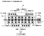
図1に示す半導体装置10において、8本のフィン活性層11(以下単に「活性層」という)がゲートコンタクト12に接続された一本のゲート電極13を横断するようにピッチ幅Hをもって配列されている。このピッチ幅Hは、隣接する活性層11の配置距離に依存する。
なお、以下の実施形態の説明において、フィン活性層やその他の構成要素の数等は一例であって、説明の便宜を図るものにすぎない。便宜上、同図中の活性層11を紙面左から順番に活性層11(1)、…、活性層11(8)のように適宜表記する(たとえば活性層11(1)は同図中に示す丸印で囲まれた番号に対応する)。後述するFinFET、電流ID等も適宜FinFET(1)、…FinFET(8)のように表記する。
In the
In the following description of the embodiments, the number of fin active layers and other components are merely examples, and are merely for convenience of description. For the sake of convenience, the
次に、図1に示す破線L1−L2間の断面について、図2(A)を中心に説明する。
活性層11(1)〜(8)は、半導体基板Aに形成されたシリコン酸化(SiO2)膜14上に突出するようにシリコン(Si)で形成され、表面がシリサイド(Silicide)化されている。
各活性層11は、シリコン酸化膜14との接触面を除く周囲がゲート絶縁膜15を挟んでゲート電極13で覆われている。ゲート電極13は、たとえばポリシリコン(poly Si)で形成されている。
同図中において、端に配置された活性層11(8)は、ゲート電極13上を覆う絶縁性の第1層間膜16の一部に開口されたコンタクトホール17を介してゲートコンタクト12と接続されている。
このコンタクトホール17および後述するコンタクトホール(図2(B)の"110","115","117","118”)は、いずれもその内部が、たとえばタングステンで充填されている。また、ゲートコンタクト12、および後述する電極111、ドレイン電極114、ソース電極116は、たとえばアルミニウムで形成され、導電体であれば特に限定されない。
Next, a cross section between broken lines L1 and L2 illustrated in FIG. 1 will be described mainly with reference to FIG.
The active layers 11 (1) to (8) are formed of silicon (Si) so as to protrude on the silicon oxide (SiO 2 )
Each
In the figure, the active layer 11 (8) disposed at the end is connected to the
The contact holes 17 and the contact holes described later ("110", "115", "117", "118" in FIG. 2B) are both filled with tungsten, for example. The
次に、図1に示す破線L3−L4間の断面について図2(B)を中心に説明する。
図1に示す活性層11(3)は、その一端にドレイン拡散層18が、他端にソース拡散層19が形成されている。
ドレイン拡散層18は、第1層間膜16に開口されたコンタクトホール110を介して電極111に接続されている。
この電極111は、その上部を覆う絶縁性の第2層間膜112に開口されたコンタクトホール113を介してドレイン電極114に接続されている。
一方、ソース拡散層19は、第1層間膜16に開口されたコンタクトホール115を介してソース電極116に接続されている。
Next, a cross section between broken lines L3-L4 shown in FIG. 1 will be described with a focus on FIG.
The active layer 11 (3) shown in FIG. 1 has a
The
The
On the other hand, the
図2(B)、図4に示すように、活性層11のドレイン拡散層18、ソース拡散層19、コンタクトホールを介してこれらの拡散層に接続されたそれぞれの電極(114,115)、ゲート絶縁膜15を挟んで形成されたゲート電極13、およびこの配線に接続されたゲートコンタクト12によって、単体のFinFETが形成されている。
As shown in FIGS. 2B and 4, the
ドレイン拡散層18およびソース拡散層19が共にn型で形成されているものとする。ゲートコンタクト12にゲート電圧VGSを、ドレイン拡散層18に正の電圧が印加されるようにドレイン電極114およびソース電極116間に電圧VDSを印加すれば、ソース拡散層19およびドレイン拡散層18間にチャネルが形成され、ドレイン拡散層18からソース拡散層19の向きにドレイン電流が流れる。
It is assumed that both the
一方、図2(B)のL3側に示す活性層11に、図1に示す共通ソース領域S(A)の一部となるソース拡散層19が形成されている。この活性層11のソース拡散層19は、第1層間膜16に開口されたコンタクトホール118を介してソース電極119に接続されている。
On the other hand, a
次に、図1に示すFinFETの配置を、図3の等価回路図に関連づけて説明する。
図1に示す8個のFinFETによって、図3に示すように、ゲートを共通とし、ソースで並列接続されたトランジスタTr1,Tr2が構成されている。
具体的には、FinFET(1)、(3)、(5)、(7)によって第1のトランジスタTr1が、FinFET(2)、(4)、(6)、(8)によって第2のトランジスタTr2が構成されている。
Next, the arrangement of the FinFET shown in FIG. 1 will be described in relation to the equivalent circuit diagram of FIG.
As shown in FIG. 3, the eight FinFETs shown in FIG. 1 constitute transistors Tr1 and Tr2 that have a common gate and are connected in parallel at the source.
Specifically, the first transistor Tr1 is formed by FinFETs (1), (3), (5), and (7), and the second transistor is formed by FinFETs (2), (4), (6), and (8). Tr2 is configured.
各々のFinFETによって、交互にトランジスタTr1、Tr2のいずれかのドレインDL,DRが構成されている。
詳細には、FinFET(1)、(3)の電極111が、コンタクトホール113を介してドレイン電極114によって共通に接続され、ドレイン領域DL(A)が形成されている。
同様に、FinFET(5)、(7)の電極111が、コンタクトホール113を介してドレイン電極114によって共通に接続され、ドレイン領域DL(B)が形成されている。
図1の説明上、ドレイン領域を「DL(A)、DL(B)」のように分けて表記しているが、ドレイン領域DL(A)とDL(B)とは、さらに上層で共通に配線接続され、図3のトランジスタTr1のドレインDL(ドレイン領域DL)を形成している。
上述と同様に、FinFET(2)、(4)の電極111によって、ドレイン領域DR(A)が、FinFET(6)、(8)電極111によって、ドレイン領域DR(B)が形成されている。
そして、ドレイン領域DR(A)とDR(B)とは、さらに上層で共通に配線接続され、図3のトランジスタTr2のドレインDR(ドレイン領域DR)を形成している。
Each FinFET alternately constitutes one of the drains DL and DR of the transistors Tr1 and Tr2.
In detail, the
Similarly, the
In the description of FIG. 1, the drain region is represented as “DL (A), DL (B)”, but the drain region DL (A) and DL (B) are more commonly used in the upper layer. The wirings are connected to form the drain DL (drain region DL) of the transistor Tr1 in FIG.
Similarly to the above, the drain region DR (A) is formed by the
Further, the drain regions DR (A) and DR (B) are connected to each other in the upper layer in common, and form the drain DR (drain region DR) of the transistor Tr2 in FIG.
一方、FinFET(1)、(3)のソース電極116が、共通に接続され、FinFET(5)、(7)のソース電極116も、共通に接続され、トランジスタTr1のソースが構成されている。
同様に、FinFET(2)、(4)のソース電極116が、共通に接続され、FinFET(6)、(8)のソース電極116も、共通に接続され、トランジスタTr2のソースが構成されている。
図3のトランジスタTr1、Tr2のソースを共通に接続するため、共に接続されたFinFET(1)、(3)のソース電極116と、共に接続されたFinFET(6)、(8)のソース電極116とが、共通に接続されて共通ソース領域S(A)が形成されている。
同様に、FinFET(2)、(4)、(5)、(7)によって、共通ソース領域S(B)が形成されている。
説明の便宜上、共通ソース領域をS(A)、S(B)のように表記したが、図3のようにトランジスタTr1、Tr2のソースSは共通に接続されている。
なお、図1中に示す区間Xを、FinFET(1)、(3)、(6)、(8)のソース電極116で接続するのではなく、活性層11にて接続するようにしてもよい。図1中に示す区間Yについても同様である。
On the other hand, the
Similarly, the
In order to connect the sources of the transistors Tr1 and Tr2 in FIG. 3 in common, the
Similarly, the common source region S (B) is formed by the FinFETs (2), (4), (5), and (7).
For convenience of explanation, the common source regions are represented as S (A) and S (B), but the sources S of the transistors Tr1 and Tr2 are commonly connected as shown in FIG.
1 may be connected not by the
このように、対をなし、並列接続されたトランジスタTr1,Tr2を1ゲート入力のペアトランジスタと称する。 Thus, the transistors Tr1 and Tr2 that are paired and connected in parallel are referred to as one-gate input pair transistors.
次に、図1の半導体装置10の動作について図5を参照しながら説明する。図5は、本実施形態に係る半導体装置の動作を説明するための図である。
Next, the operation of the
ゲートコンタクト12にゲート電圧VGSを、各活性層11のドレイン拡散層18に正の電圧が印加されるように、各ドレイン領域DL、DRの各ドレイン電極114と、各共通ソース領域S(A)、S(B)との間に電圧VDSを印加すれば、ソース拡散層19およびドレイン拡散層18間にチャネルが形成され、図5のようにドレイン拡散層18からソース拡散層19の向きに電流IDが流れる(図中の矢印は電流IDの向きを示す)。
The
具体的には、FinFET(1)には電流ID(1)が、FinFET(3)には電流ID(3)が、それぞれドレイン領域DL(A)から共通ソース領域S(A)の向きに流れる。
FinFET(2)には電流ID(2)が、FinFET(4)には電流ID(4)が
、それぞれドレイン領域DR(A)から共通ソース領域S(B)の向きに流れる。
FinFET(5)には電流ID(5)が、FinFET(7)には電流ID(7)が
、それぞれドレイン領域DL(B)から共通ソース領域S(B)の向きに流れる。
FinFET(6)には電流ID(6)が、FinFET(8)には電流ID(8)が
、それぞれドレイン領域DR(B)から共通ソース領域S(A)の向きに流れる。
Specifically, the current ID (1) flows through the FinFET (1) and the current ID (3) flows through the FinFET (3) from the drain region DL (A) to the common source region S (A). .
The current ID (2) flows through the FinFET (2) and the current ID (4) flows through the FinFET (4) in the direction from the drain region DR (A) to the common source region S (B).
A current ID (5) flows through the FinFET (5) and a current ID (7) flows through the FinFET (7) from the drain region DL (B) to the common source region S (B).
A current ID (6) flows through the FinFET (6) and a current ID (8) flows through the FinFET (8) in the direction from the drain region DR (B) to the common source region S (A).
しかし、電流ID(1)、(3)の電流方向と、電流ID(5)、(7)の電流方向は互いに逆向きであり、同様に、電流ID(2)、ID(4)の電流方向と、電流ID(6)、ID(8)の電流方向もまた、互いに逆向きとなる。 However, the current directions of the current IDs (1) and (3) and the current directions of the current IDs (5) and (7) are opposite to each other. Similarly, the currents of the current IDs (2) and ID (4) The direction and the current direction of current ID (6), ID (8) are also opposite to each other.
図1のようにFinFETを配列し、接続することで、トランジスタTr1およびTr2が対をなすペアトランジスタにおいても、全体的に電流方向の整合性をとることができる。
本実施形態により、電流方向の違いによるプロセスの起因による影響を防止でき、無駄なくFinFETを配置できるため、トランジスタ間のピッチ幅を小さく取ることができる。
By arranging FinFETs as shown in FIG. 1 and connecting them, even in the paired transistors in which the transistors Tr1 and Tr2 form a pair, the matching in the current direction can be obtained as a whole.
According to the present embodiment, it is possible to prevent the influence caused by the process due to the difference in the current direction, and the FinFET can be disposed without waste, so that the pitch width between the transistors can be reduced.
(第1実施形態の変形例)
次に、第1実施形態の変形例について説明する。図6は、本実施形態に係る半導体装置の変形例を示す平面図である。
図6に示す半導体装置10aのように、ゲート電極13の両端にゲートコンタクト12、12aが接続されていてもよい。これに伴い、ゲートコンタクト12aはコンタクトホール17bを介してゲート電極13に接続されている。
(Modification of the first embodiment)
Next, a modification of the first embodiment will be described. FIG. 6 is a plan view showing a modification of the semiconductor device according to the present embodiment.
本実施形態では、2個のFinFETのソース・ドレイン同士を接続する例を挙げたが、3個以上のFinFETのソース・ドレイン同士を接続してもよい。この場合、ゲート電極13を横切るFinFETの数は少なくとも12個となる。
In this embodiment, an example in which the sources and drains of two FinFETs are connected to each other has been described. However, the sources and drains of three or more FinFETs may be connected to each other. In this case, the number of FinFETs that cross the
(第2実施形態)
図7は、本実施形態に係る半導体装置の一例を示す平面図である。図8は、図7に示す半導体装置の等価回路図である。
(Second Embodiment)
FIG. 7 is a plan view showing an example of the semiconductor device according to the present embodiment. FIG. 8 is an equivalent circuit diagram of the semiconductor device shown in FIG.
半導体装置10bは、2つのゲートコンタクト12a1、12a2を有し、図8に示すように、各々のゲートを独立に制御するペアトランジスタが構成されている。本実施形態では、3つの共通ソース領域S(A)、S(B)、S(C)を設けることで、図8に示すペアトランジスタを実現している。以下、第1実施形態と異なる点について説明する。
The semiconductor device 10b is 1 two
図8に示すように、ゲート入力が独立し、ソースで並列接続されたトランジスタTr1a,Tr2aが構成されている。
具体的には、FinFET(1)、(3)、(5)、(7)によってトランジスタTr1aが、FinFET(2)、(4)、(6)、(8)によってトランジスタTr2aが構成されている。
As shown in FIG. 8, transistors Tr1a and Tr2a having independent gate inputs and connected in parallel at the source are configured.
Specifically, the transistor Tr1a is configured by the FinFETs (1), (3), (5), and (7), and the transistor Tr2a is configured by the FinFETs (2), (4), (6), and (8). .
ドレイン領域DL(A)、(B)、およびドレイン領域DR(A)、(B)の形成場所は、第1実施形態と異なるが、各々のドレイン領域に接続されているFinFETは第1実施形態と同じである。 The formation locations of the drain regions DL (A) and (B) and the drain regions DR (A) and (B) are different from those of the first embodiment, but the FinFET connected to each drain region is the first embodiment. Is the same.
第1実施形態とは異なり、図8のトランジスタTr1a、Tr2aのソースを共通に接続するため、共に接続されたFinFET(1)、(3)のソース電極116と、共に接続されたFinFET(2)、(4)のソース電極116とが、さらに共通に接続されて共通ソース領域S(A)が形成されている。
同様に、FinFET(5)、(7)によって、共通ソース領域S(B)が形成され、FinFET(6)、(8)によって、共通ソース領域S(C)が形成されている。
図7のように、各々のFinFETを配置し、接続することで、図8のようにソースSが共通に接続されている。
Unlike the first embodiment, since the sources of the transistors Tr1a and Tr2a in FIG. 8 are connected in common, the FinFET (1) connected together, the
Similarly, the common source region S (B) is formed by FinFETs (5) and (7), and the common source region S (C) is formed by FinFETs (6) and (8).
By arranging and connecting each FinFET as shown in FIG. 7, the sources S are connected in common as shown in FIG.
図8に示すトランジスタTr1のゲートは、FinFET(1)、(3)、(5)、(7)のゲート電極13a1がゲートコンタクト12a1に共通に接続されて形成されている。
同様に、トランジスタTr2のゲートは、FinFET(2)、(4)、(6)、(8)のゲート電極13a2がゲートコンタクト12a2に共通に接続されて形成されている。
The gate of the transistor Tr1 shown in FIG. 8, FinFET (1), (3 ), (5), is formed is connected to the common gate electrode 13a 1 is the
Similarly, the gate of the transistor Tr2, FinFET (2), (4), (6), are formed is connected to the common gate electrode 13a 2 is the
このような対をなすペアトランジスタを2入力ゲートのペアトランジスタと称する。 Such a paired transistor is referred to as a two-input gate pair transistor.
図7に示すように、ゲートコンタクト12にゲート電圧VGSを、各活性層11のドレイン拡散層18に正の電圧が印加されるように、各ドレイン領域DL(A)、(B)、DR(A)、(B)の各ドレイン電極114と、各共通ソース領域S(A)〜S(C)との間に電圧VDSを印加すれば、ソース拡散層19およびドレイン拡散層18間にチャネルが形成され、ドレイン拡散層18からソース拡散層19の向きに電流IDが流れる。
As shown in FIG. 7, each drain region DL (A), (B), DR is applied so that a gate voltage V GS is applied to the
具体的には、電流ID(1)、(3)が、それぞれドレイン領域DL(A)から共通ソース領域S(A)の向きに流れ、電流ID(2)、(4)が、それぞれドレイン領域DR(A)から共通ソース領域S(A)の向きに流れる。
電流ID(5)、(7)が、それぞれドレイン領域DL(B)から共通ソース領域S(B)の向きに流れ、電流ID(6)、(8)が、それぞれドレイン領域DR(B)から共通ソース領域S(C)の向きに流れる。
Specifically, currents ID (1) and (3) flow from the drain region DL (A) to the common source region S (A), respectively, and currents ID (2) and (4) respectively flow into the drain region. It flows in the direction from the DR (A) to the common source region S (A).
Currents ID (5) and (7) flow in the direction from the drain region DL (B) to the common source region S (B), and currents ID (6) and (8) flow from the drain region DR (B), respectively. It flows in the direction of the common source region S (C).
しかし、電流ID(1)、(3)の電流方向と、電流ID(5)、(7)の電流方向は互いに逆向きであり、同様に、電流ID(2)、ID(4)の電流方向と、電流ID(6)、ID(8)の電流方向もまた、互いに逆向きである。 However, the current directions of the current IDs (1) and (3) and the current directions of the current IDs (5) and (7) are opposite to each other. Similarly, the currents of the current IDs (2) and ID (4) The direction and the current direction of current ID (6), ID (8) are also opposite to each other.
図7のようにFinFETを配列し、接続することで、トランジスタTr1aおよびTr2aが対をなすペアトランジスタにおいても、全体的に電流方向の整合性をとることができる。
本実施形態により、電流方向の違いによるプロセスの起因による影響を防止でき、無駄なくFinFETを配置できるため、トランジスタ間のピッチ幅Hを小さく取ることができる。
By arranging and connecting FinFETs as shown in FIG. 7, even in the paired transistors in which the transistors Tr1a and Tr2a form a pair, it is possible to achieve overall matching in the current direction.
According to the present embodiment, it is possible to prevent the influence of the process caused by the difference in the current direction, and the FinFET can be disposed without waste, so that the pitch width H between the transistors can be reduced.
(第2実施形態の変形例)
次に、第2実施形態の変形例について説明する。図9は、本実施形態に係る半導体装置の変形例を示す平面図である。
図9に示す半導体装置10cように、ゲート電極13a1の両端にゲートコンタクト12a1、12c1が、ゲート電極13a2の両端にゲートコンタクト12a2、12C2がそれぞれ接続されていてもよい。これに伴い、ゲートコンタクト12c1はコンタクトホール17c1を介してゲート電極13a1に、ゲートコンタクト12c2はコンタクトホール17c2を介してゲート電極13a2にそれぞれ接続されている。
(Modification of the second embodiment)
Next, a modification of the second embodiment will be described. FIG. 9 is a plan view showing a modification of the semiconductor device according to the present embodiment.
The
(第3実施形態)
図10は、本実施形態に係る半導体装置の一例を示す平面図である。図11(A)は、図1に示す半導体装置の断面図であり、図11(B)は、図10に示す半導体装置の断面図である。ただし、図11(A),(B)とも、図10に示すAの方向からみたものであり、半導体基板A上の活性層11のみを示している。
(Third embodiment)
FIG. 10 is a plan view showing an example of the semiconductor device according to the present embodiment. 11A is a cross-sectional view of the semiconductor device illustrated in FIG. 1, and FIG. 11B is a cross-sectional view of the semiconductor device illustrated in FIG. However, both FIGS. 11A and 11B are viewed from the direction A shown in FIG. 10, and only the
半導体装置10dは、図1に示す半導体装置10(1入力ゲートのペアトランジスタ)の活性層11の両端にダミー(疑似)のダミー活性層120a、120bを形成したものである。ダミー活性層120a、120bは、他の活性層11と同様にゲート電極13の下層に形成されている。
The
図11(A)のように、2つのダミー活性層120a、120bを形成しない場合、活性層11の繰り返しパターンが途切れ、活性層11(1)および活性層11(8)は、他の活性層11と比較してリソグラフィ的な要因によりパターン崩れを起こしやすくなる。
そこで、図11(B)に示す本実施形態のように、活性層11(1)の片側にダミー活性層120aを、活性層11(8)の片側にダミー活性層120bを、それぞれ形成することにより、両端の活性層11(1)および活性層11(8)のパターン崩れを防止できる。
When the two dummy
Therefore, as in the present embodiment shown in FIG. 11B, the dummy
(第4実施形態)
図12は、本実施形態に係る半導体装置の一例を示す平面図である。
(Fourth embodiment)
FIG. 12 is a plan view showing an example of the semiconductor device according to the present embodiment.
半導体装置10eは、図7に示す半導体装置10b(2入力ゲートのペアトランジスタ)の活性層11の両端に、第3実施形態と同様の理由で、ダミーのダミー活性層120a、120bを形成したものである。ダミー活性層120は、他の活性層11と同様にゲート電極13の下層に形成されている。
In the semiconductor device 10e, dummy dummy
本実施形態においても、第3実施形態と同様にダミー活性層120a、120bを設けることで、両端の活性層11(1)および活性層11(8)のパターン崩れを防止できる。
Also in this embodiment, by providing the dummy
(第5実施形態)
図13は、本実施形態に係る半導体装置の一例を示す平面図である。図14(A)は、図1に示す半導体装置の断面図であり、図14(B)は、図13に示す半導体装置の断面図である。ただし、図14(A),(B)とも、図13に示すAの方向からみたものであり、半導体基板A上のゲート電極13のみを示している。
(Fifth embodiment)
FIG. 13 is a plan view showing an example of the semiconductor device according to the present embodiment. 14A is a cross-sectional view of the semiconductor device illustrated in FIG. 1, and FIG. 14B is a cross-sectional view of the semiconductor device illustrated in FIG. However, both FIGS. 14A and 14B are viewed from the direction A shown in FIG. 13, and only the
半導体装置10fは、図1に示す半導体装置10(1入力ゲートのペアトランジスタ)にダミーゲート電極121a、121bを形成したものである。ダミーゲート電極121a、121bは、ゲート電極13と平行に共通ソース領域S(A)、S(B)の脇に形成されている。
The
図14(A)のように、2本のダミーゲート電極121a、121bを形成しない場合、ゲート電極13が孤立状態となり、リソグラフィ的な要因によりパターン崩れを起こしやすくなる。
そこで、図14(B)に示す本実施形態のように、ゲート電極13の両脇にダミーゲート電極121a、121bをそれぞれ形成することにより、ゲート電極13のパターン崩れを防止できる。
As shown in FIG. 14A, when the two
Therefore, as in the present embodiment shown in FIG. 14B, the pattern collapse of the
(第6実施形態)
図15は、本実施形態に係る半導体装置の一例を示す平面図である。
(Sixth embodiment)
FIG. 15 is a plan view showing an example of the semiconductor device according to the present embodiment.
半導体装置10gは、図7に示す半導体装置10aにダミー(疑似)のダミーゲート電極121a、121bを形成したものである。ダミーゲート電極121a、121bは、ゲート電極13a1、13a1と平行に共通ソース領域S(A)、S(B)の脇に形成されている。
The
本実施形態においても、第5実施形態と同様にダミーゲート電極121a、121bを設けることで、ゲート電極13a1、13a1のパターン崩れを防止できる。
Also in this embodiment, by providing the
(第7実施形態)
図16は、本実施形態に係る半導体装置の一例を示す平面図である。
(Seventh embodiment)
FIG. 16 is a plan view showing an example of the semiconductor device according to the present embodiment.
第1〜第6実施形態では、トランジスタTr1のドレインDLを形成するドレイン領域DL(図3参照)と、Tr2のドレインDRを形成するドレイン領域DRのサイズ比が同等であったため、トランジスタTr1とTr2とのサイズ比も同等であったが、FinFETの配置によっては、活性層11の数を調整できず、このサイズ比が1対1にならない場合が生じ、一部の領域で電流IDが打ち消されない場合がある。
半導体装置10hでは、トランジスタTr1とTr2とのサイズ比が3対1となる場合の1入力ゲートのペアトランジスタを例に挙げて、全体的に電流方向の整合性をとる方法について説明する。
In the first to sixth embodiments, since the size ratio of the drain region DL (see FIG. 3) that forms the drain DL of the transistor Tr1 and the drain region DR that forms the drain DR of the Tr2 is equal, the transistors Tr1 and Tr2 However, depending on the arrangement of FinFETs, the number of
In the
本実施形態では、たとえばサイズ比が3対1であった場合、サイズ比が1対1となるようなFinFETで構成される領域REG1と、サイズが大きい(小さい)、いわば余剰分としてのFinFETで構成される領域REG2とに分ける。
図16に示す「L」は、ドレイン領域DLから流れる電流IDを、「R」は、ドレイン領域DRから流れる電流IDを示しており、FinFET(1)、(3)、およびFinFET(5)〜(8)によってトランジスタTr1が、FinFET(2)、(4)によってトランジスタTr2が形成されている。
In the present embodiment, for example, when the size ratio is 3: 1, the region REG1 is configured by FinFETs having a size ratio of 1: 1, and the size is large (small). The area REG2 is divided.
In FIG. 16, “L” indicates the current ID flowing from the drain region DL, “R” indicates the current ID flowing from the drain region DR, and FinFETs (1), (3), and FinFETs (5) ˜ The transistor Tr1 is formed by (8), and the transistor Tr2 is formed by FinFETs (2) and (4).
したがって、トランジスタTr1,Tr2のサイズは異なるが、領域REG1においては、各々のFinFETが互いに異なるドレイン領域を形成し、FinFET(1)、(4)によって共通ソース領域S(A)が、FinFET(2)、(3)によって共通ソース領域S(B)が形成されているため、トランジスタTr1とTr2とのサイズ比は1対1である。
領域REG2においては、すべてのFinFETがトランジスタTr1のドレイン領域DLを形成しているが、トランジスタTr1のドレイン領域DL側から流れる電流IDの極性が0となるように、FinFET(5)、(7)によって共通ソース領域S(C)が、FinFET(6)、(8)によって共通ソース領域S(D)が対称性をもって形成されている。
Therefore, although the sizes of the transistors Tr1 and Tr2 are different, in the region REG1, each FinFET forms a different drain region, and the FinFETs (1) and (4) make the common source region S (A) the FinFET (2 ) And (3) form the common source region S (B), and the size ratio between the transistors Tr1 and Tr2 is 1: 1.
In the region REG2, all the FinFETs form the drain region DL of the transistor Tr1, but the FinFETs (5) and (7) have the polarity of the current ID flowing from the drain region DL side of the transistor Tr1 being zero. The common source region S (C) is formed symmetrically by FinFETs (6) and (8).
このように、領域REG2においても、電流IDの極性を考慮してFinFETを配線接続することで、プロセスの起因による影響を防止でき、全体的に電流方向の整合性をとることができる。
なお、トランジスタTr1とTr2とのサイズ比が1対4等の場合でも、本実施形態が好適に適用できる。
As described above, also in the region REG2, by considering the polarity of the current ID and connecting the FinFETs, the influence due to the process can be prevented, and overall consistency in the current direction can be obtained.
Note that the present embodiment can be suitably applied even when the size ratio between the transistors Tr1 and Tr2 is 1: 4.
(第7実施形態の変形例)
次に、本実施形態の変形例について説明する。図17は、本実施形態に係る半導体装置の変形例を示す平面図である。
図17に示す半導体装置10iのように、領域REG2のFinFETを配線接続してもよい。
具体的には、領域REG2において、トランジスタTr1のドレイン領域DL側から流れる電流IDの極性が0となるように、FinFET(5)、(6)によって共通ソース領域S(C)が、FinFET(7)、(8)によって共通ソース領域S(D)が対称性をもって形成されている。
(Modification of the seventh embodiment)
Next, a modification of this embodiment will be described. FIG. 17 is a plan view showing a modification of the semiconductor device according to the present embodiment.
As in the semiconductor device 10i illustrated in FIG. 17, the FinFETs in the region REG2 may be connected by wiring.
Specifically, in the region REG2, the common source region S (C) is defined by the FinFET (7) by the FinFETs (5) and (6) so that the polarity of the current ID flowing from the drain region DL side of the transistor Tr1 becomes zero. ) And (8), the common source region S (D) is formed with symmetry.
図16、図17のようにFinFETを配列し、接続することで、サイズ比が異なるペアトランジスタにおいても、全体的に電流方向の整合性をとることができる。 By arranging and connecting FinFETs as shown in FIGS. 16 and 17, even in paired transistors having different size ratios, it is possible to achieve matching in the current direction as a whole.
(第8実施形態)
図18は、本実施形態に係る半導体装置の一例を示す平面図である。
(Eighth embodiment)
FIG. 18 is a plan view showing an example of a semiconductor device according to the present embodiment.
本実施形態は、第7実施形態のようにドレイン領域DLとDRとのサイズ比が3対1となる場合の2入力ゲートのペアトランジスタを例に挙げて説明する。 In the present embodiment, a pair transistor of a two-input gate when the size ratio of the drain regions DL and DR is 3: 1 as in the seventh embodiment will be described as an example.
図18に示すように、FinFET(1)、(3)、およびFinFET(5)〜(8)によってトランジスタTr1aが、FinFET(2)、(4)によってトランジスタTr2aが形成されている。 As shown in FIG. 18, a transistor Tr1a is formed by FinFETs (1) and (3) and FinFETs (5) to (8), and a transistor Tr2a is formed by FinFETs (2) and (4).
領域REG1においては、各々のFinFETが互いに異なるドレイン領域を形成し、FinFET(1)、(2)によって共通ソース領域S(A)が、FinFET(3)によって共通ソース領域S(B)が、FinFET(4)によって共通ソース領域S(C)が形成されている。
領域REG2において、すべてのFinFETが同じドレイン領域DLを形成し、トランジスタTr1aのドレイン領域DL側から流れる電流IDの極性が0となるように、FinFET(5)、(7)によって共通ソース領域S(D)が、FinFET(6)、(8)によって共通ソース領域S(E)が対称性をもって形成されている。
In the region REG1, each FinFET forms a different drain region, the FinFETs (1) and (2) form the common source region S (A), the FinFET (3) forms the common source region S (B), and the FinFET. A common source region S (C) is formed by (4).
In the region REG2, all the FinFETs form the same drain region DL, and the common source region S () is obtained by the FinFETs (5) and (7) so that the polarity of the current ID flowing from the drain region DL side of the transistor Tr1a becomes zero. D), the common source region S (E) is formed with symmetry by the FinFETs (6) and (8).
このように、領域REG2においても、電流IDの極性を考慮してFinFETを配線接続することで、プロセスの起因による影響を防止でき、全体的に電流方向の整合性をとることができる。 As described above, also in the region REG2, by considering the polarity of the current ID and connecting the FinFETs, the influence due to the process can be prevented, and overall consistency in the current direction can be obtained.
(第8実施形態の変形例)
次に、本実施形態の変形例について説明する。図19は、本実施形態に係る半導体装置の変形例を示す平面図である。
図19に示す半導体装置10kのように、領域REG2のFinFETを配線接続してもよい。
具体的には、領域REG1における各々のFinFETは、たとえば図7に示すFinFET(1)〜(4)と同様に配線接続されている。
領域REG2において、トランジスタTr1aのドレイン領域DL側から流れる電流IDの極性が0となるように、FinFET(5)、(6)は領域REG1の共通ソース領域S(A)、およびドレイン領域D(B)を形成し、FinFET(7)、(8)によって共通ソース領域S(B)、ドレイン領域D(C)が対称性をもって形成されている。
(Modification of the eighth embodiment)
Next, a modification of this embodiment will be described. FIG. 19 is a plan view showing a modification of the semiconductor device according to the present embodiment.
As in the semiconductor device 10k shown in FIG. 19, the FinFETs in the region REG2 may be connected by wiring.
Specifically, each FinFET in the region REG1 is connected by wiring, for example, similarly to the FinFETs (1) to (4) shown in FIG.
In the region REG2, FinFETs (5) and (6) are common source regions S (A) and drain regions D (B) of the region REG1 so that the polarity of the current ID flowing from the drain region DL side of the transistor Tr1a becomes zero. ), And the common source region S (B) and the drain region D (C) are formed symmetrically by the FinFETs (7) and (8).
図18、図19のようにFinFETを配列し、接続することで、サイズ比が異なるペアトランジスタにおいても、プロセスの起因による影響を防止でき、全体的に電流方向の整合性をとることができる。 By arranging and connecting FinFETs as shown in FIG. 18 and FIG. 19, even in pair transistors having different size ratios, the influence due to the process can be prevented and overall current direction consistency can be achieved.
(第9実施形態)
図20は、本実施形態に係る半導体装置の一例を示す平面図である。
(Ninth embodiment)
FIG. 20 is a plan view showing an example of the semiconductor device according to the present embodiment.
本実施形態は、半導体基板の方位による影響を低減させるように、図1に示す2つの半導体装置10を配置したものである。
具体的には、図20に示す半導体装置20は、各々の半導体装置10が含むペアトランジスタを形成するフィン活性層11の向きが互いに垂直となるように半導体基板上に形成されている。
このような配置形態をとることで、電流による基板方位の影響を低減させることができる。
本実施形態では、1入力ゲートのペアトランジスタを例に挙げたが、2入力ゲートのペアトランジスタをはじめ、ダミー活性層やダミー配線層をとる構成であってもよく、種々の組み合わせが可能である。
In the present embodiment, two
Specifically, the
By adopting such an arrangement, the influence of the substrate orientation due to the current can be reduced.
In the present embodiment, a pair transistor with one input gate has been described as an example. However, a pair of two input gate transistors, a dummy active layer and a dummy wiring layer may be used, and various combinations are possible. .
以上、本実施形態によれば、各々が複数のフィントランジスタで形成された第1のトランジスタTr1および第2のトランジスタTr2を有し、第1のトランジスタTr1および第2のトランジスタTr2のソースを電気的に共有するように接続された半導体装置であって、複数のフィントランジスタFinFETは、半導体基板上Aに突出し、チャネル領域を形成するように一端に上記ソースとなるソース拡散層19が形成され、他端にドレイン拡散層18が形成されたフィン活性層11を各々有する。
各々のフィン活性層11は、互いが平行に隣接するように配列され、複数のフィントランジスタFinFETは、各々の第1のトランジスタTr1および上記第2のトランジスタTr2において、電流の流れる向きが互いに逆向きとなるようにドレイン層DL,DRが配置されていることから、無駄なくペアトランジスタを配置できるだけでなく、活性層間のピッチ幅を短くすることもできるという利点がある。
ペアトランジスタの形成する各々のトランジスタ間で電流方向のプロセスに起因する影響をキャンセルでき、整合性が向上するという利点がある。
As described above, according to the present embodiment, the first transistor Tr1 and the second transistor Tr2 each having a plurality of fin transistors are provided, and the sources of the first transistor Tr1 and the second transistor Tr2 are electrically connected. The plurality of fin transistors FinFETs project on the semiconductor substrate A, and the
The fin
There is an advantage that the influence caused by the process in the current direction can be canceled between the transistors formed by the pair transistors, and the matching is improved.
なお、FinFETの配置や配線方法は、上述の実施形態に限定されず、本発明の要旨を変更しない範囲内で様々な改変が可能である。 Note that the FinFET arrangement and wiring method are not limited to the above-described embodiments, and various modifications can be made without departing from the scope of the present invention.
10…半導体装置、11…フィン活性層、12…ゲートコンタクト、13…ゲート電極、14…シリコン酸化膜、15…ゲート絶縁膜、16…第1層間膜、17…コンタクトホール、18…ドレイン拡散層、19…ソース拡散層、20…半導体装置、110、113、115、117、118…コンタクトホール、111…電極、112…第2層間膜、114…ドレイン電極、116、119…ソース電極、120…ダミー活性層、121…ダミーゲート電極、DL…トランジスタTr1,Tr1aのドレイン(領域)、DR…トランジスタTr2,Tr2aドレイン(領域)、S…共通ソース(領域)
DESCRIPTION OF
Claims (11)
フィントランジスタを用いた第1のトランジスタ及び第2のトランジスタからなるペアトランジスタを有し、
奇数番目のフィントランジスタで構成された前記第1のトランジスタおよび偶数番目のフィントランジスタで構成された前記第2のトランジスタのソースが共通に接続され、前記第1および第2のトランジスタのゲートが共通に接続され、
各フィントランジスタは、
半導体基板上に突出したフィン活性層を有し、
各フィン活性層は、
当該フィン活性層の表面領域に存在するソース領域と、
チャネル領域を形成可能に前記表面領域において前記ソース領域から離間した位置に存在するドレイン領域と、
を有し、
前記各フィン活性層は、当該フィン活性層のサイズが各々同一または略同一であって、前記各フィン活性層の前記ソース領域および前記ドレイン領域間の前記チャネル領域に流れる電流が各々平行となるように、一列に一定間隔で配列され、
前記第1のトランジスタ及び前記第2のトランジスタは、各々2m個(mは2以上の整数)のフィン活性層で構成され、前記ペアトランジスタは、全体で4m個のフィン活性層を有しており、
前記第1のトランジスタを構成する各フィン活性層には、1番目から2m−1番目のフィン活性層の各チャネル領域に流れる電流の向きが、2m+1番目から4m−1番目のフィン活性層の各チャネル領域に流れる電流の向きと逆向きになるように、前記ドレイン領域および前記ソース領域が配置され、
前記第2のトランジスタを構成する各フィン活性層には、2番目から2m番目のフィン活性層の各チャネル領域に流れる電流の向きが、2m+2番目から4m番目のフィン活性層の各チャネル領域に流れる電流の向きと逆向きになるように、前記ドレイン領域および前記ソース領域が配置され、
前記第1のトランジスタを構成する各フィン活性層の各ドレイン領域が、共通に接続され、
前記第2のトランジスタを構成する各フィン活性層の各ドレイン領域が、共通に接続され、
前記各フィン活性層の各ソース領域が、共通に接続されている
半導体装置。 A semiconductor device having a pair transistor of one input gate,
A pair transistor composed of a first transistor and a second transistor using a fin transistor;
Odd of the source of the second transistor constituted by the first transistor and the even-numbered fins transistor constituted by the fin transistors are connected in common, the common gate of the first and second transistors Connected,
Each fin transistor
A fin active layer protruding on the semiconductor substrate;
Each fin active layer
A source region present in the surface region of the fin active layer;
A drain region present at a position spaced from the source region in the surface region so as to form a channel region;
Have
Each fin active layer has the same or substantially the same size of the fin active layer, and currents flowing in the channel region between the source region and the drain region of each fin active layer are parallel to each other. Are arranged in a row at regular intervals,
Each of the first transistor and the second transistor is composed of 2m fin active layers (m is an integer of 2 or more), and the pair transistors have a total of 4m fin active layers. ,
Each fin active layer constituting the first transistor has a direction of current flowing in each channel region of the 1st to 2m−1 fin active layers, and each of the 2m + 1 to 4m−1 fin active layers. The drain region and the source region are arranged so as to be opposite to the direction of current flowing in the channel region,
Wherein the second fins active layer constituting the transistor, the direction of the current flowing from the second into the channel region of 2m th fin activation layer flows from 2m + 2 -th each channel region of 4m th fin activation layer The drain region and the source region are arranged so as to be opposite to the direction of current,
Each drain region of each fin active layer constituting the first transistor is connected in common,
The drain regions of the fin active layers constituting the second transistor are connected in common,
A semiconductor device in which the source regions of the fin active layers are connected in common.
前記ソース領域および前記ドレイン領域間の前記フィン活性層上に絶縁膜を介して存在するゲート電極を有し、
各ゲート電極が、前記各フィン活性層の配列方向に延在するように共通に接続されている
請求項1記載の半導体装置。 Each of the fin transistors is
A gate electrode present on the fin active layer between the source region and the drain region via an insulating film;
The semiconductor device according to claim 1, wherein the gate electrodes are connected in common so as to extend in the arrangement direction of the fin active layers.
フィントランジスタを用いた第1のトランジスタ及び第2のトランジスタからなるペアトランジスタを有し、
奇数番目のフィントランジスタで構成された前記第1のトランジスタおよび偶数番目のフィントランジスタで構成された前記第2のトランジスタのソースが共通に接続され、
各フィントランジスタは、
半導体基板上に突出したフィン活性層を有し、
各フィン活性層は、
当該フィン活性層の表面領域に存在するソース領域と、
チャネル領域を形成可能に前記表面領域において前記ソース領域から離間した位置に存在するドレイン領域と、
を有し、
前記各フィン活性層は、当該フィン活性層のサイズが各々同一または略同一であって、前記各フィン活性層の前記ソース領域および前記ドレイン領域間の前記チャネル領域に流れる電流が各々平行となるように、一列に一定間隔で配列され、
前記第1のトランジスタ及び前記第2のトランジスタは、各々2m個(mは2以上の整数)のフィン活性層で構成され、前記ペアトランジスタは、全体で4m個のフィン活性層を有しており、
前記第1のトランジスタを構成する各フィン活性層には、1番目から2m−1番目のフィン活性層の各チャネル領域に流れる電流の向きが、2m+1番目から4m−1番目のフィン活性層の各チャネル領域に流れる電流の向きと逆向きになるように、前記ドレイン領域および前記ソース領域が配置され、
前記第2のトランジスタを構成する各フィン活性層には、2番目から2m番目のフィン活性層の各チャネル領域に流れる電流の向きが、2m+2番目から4m番目のフィン活性層の各チャネル領域に流れる電流の向きと逆向きになるように、前記ドレイン領域および前記ソース領域が配置され、
前記第1のトランジスタを構成する各フィン活性層の各ドレイン領域が、共通に接続され、
前記第2のトランジスタを構成する各フィン活性層の各ドレイン領域が、共通に接続され、
前記各フィン活性層の各ソース領域が、共通に接続されている
半導体装置。 A semiconductor device having a pair transistor of two input gates,
Has a transistor pair of a first transistor and a second transistor including a fin transistor,
The source of the odd-numbered of the configured fin transistor first transistor and the even-numbered second transistor constituted by the fin transistors are commonly connected,
Each fin transistor
A fin active layer protruding on the semiconductor substrate;
Each fin active layer
A source region present in the surface region of the fin active layer;
A drain region present at a position spaced from the source region in the surface region so as to form a channel region;
Have
Each fin active layer has the same or substantially the same size of the fin active layer, and currents flowing in the channel region between the source region and the drain region of each fin active layer are parallel to each other. Are arranged in a row at regular intervals,
Each of the first transistor and the second transistor is composed of 2m fin active layers (m is an integer of 2 or more), and the pair transistors have a total of 4m fin active layers. ,
Each fin active layer constituting the first transistor has a direction of current flowing in each channel region of the 1st to 2m−1 fin active layers, and each of the 2m + 1 to 4m−1 fin active layers. The drain region and the source region are arranged so as to be opposite to the direction of current flowing in the channel region,
Wherein the second fins active layer constituting the transistor, the direction of the current flowing from the second into the channel region of 2m th fin activation layer flows from 2m + 2 -th each channel region of 4m th fin activation layer The drain region and the source region are arranged so as to be opposite to the direction of current,
Each drain region of each fin active layer constituting the first transistor is connected in common,
The drain regions of the fin active layers constituting the second transistor are connected in common,
A semiconductor device in which the source regions of the fin active layers are connected in common.
前記ソース領域および前記ドレイン領域間の前記フィン活性層上に絶縁膜を介して位置するゲート電極を有し、
前記第1のトランジスタを構成するフィントランジスタの各ゲート電極が、前記各フィン活性層の配列方向に延在するように共通に接続され、
前記第2のトランジスタを構成するフィントランジスタの各ゲート電極が、前記各フィン活性層の配列方向に延在するように共通に接続されている
請求項3記載の半導体装置。 Each of the fin transistors is
A gate electrode located on the fin active layer between the source region and the drain region via an insulating film;
The gate electrodes of the fin transistors constituting the first transistor are connected in common so as to extend in the arrangement direction of the fin active layers,
4. The semiconductor device according to claim 3, wherein the gate electrodes of the fin transistors constituting the second transistor are connected in common so as to extend in the arrangement direction of the fin active layers.
前記第1の擬似活性層が、一端に配置されているフィン活性層を基準としたときに、前記各フィン活性層の配列方向に対して前記各フィン活性層の方向と逆向きに、前記一端に配置されているフィン活性層と並列に配置され、
前記第2の擬似活性層が、他端に配置されているフィン活性層を基準としたときに、前記各フィン活性層の配列方向に対して前記各フィン活性層の方向と逆向きに、前記他端に配置されているフィン活性層と並列に配置されている
請求項1から4のいずれか一に記載の半導体装置。 Is electrically disconnected from the previous SL each fin activation layer, to maintain the form of each of the fin activation layer has a first pseudo-active layer and the second pseudo active layer,
When the first pseudo active layer is based on the fin active layer disposed at one end, the one end is opposite to the direction of the fin active layer with respect to the arrangement direction of the fin active layers. Arranged in parallel with the fin active layer arranged in
When the second pseudo active layer is based on the fin active layer arranged at the other end, the direction of the fin active layer is opposite to the direction of the fin active layer with respect to the arrangement direction of the fin active layers. The semiconductor device as described in any one of Claim 1 to 4 arrange | positioned in parallel with the fin active layer arrange | positioned at the other end.
前記第1および第2の擬似ゲート電極が、前記ゲート電極の延在方向に対して各々並列に、前記各フィントランジスタを挟むように配置されている
請求項2または4記載の半導体装置。 Is electrically disconnected from the previous SL each fin activation layer, maintains the shape of the gate electrode has a first pseudo gate electrode and the second pseudo gate electrode,
Wherein the first and second pseudo gate electrode, wherein each parallel to the extending direction of the gate electrode, the semiconductor device according to claim 2 or 4 wherein is placed so as to sandwich the fins transistor.
フィントランジスタを用いた第1のトランジスタ及び第2のトランジスタからなるペアトランジスタを有し、
フィントランジスタで構成された前記第1のトランジスタおよびフィントランジスタで構成された前記第2のトランジスタのソースが共通に接続され、前記第1および第2のトランジスタのゲートが共通に接続され、
各フィントランジスタは、
半導体基板上に突出したフィン活性層を有し、
各フィン活性層は、
当該フィン活性層の表面領域に存在するソース領域と、
チャネル領域を形成可能に前記表面領域において前記ソース領域から離間した位置に存在するドレイン領域と、
を有し、
前記各フィン活性層は、当該フィン活性層のサイズが各々同一または略同一であって、前記各フィン活性層の前記ソース領域および前記ドレイン領域間の前記チャネル領域に流れる電流が各々平行となるように、一列に一定間隔で配列され、
前記第1のトランジスタのサイズが、前記第2のトランジスタのサイズと異なる半導体装置であって、
前記各フィン活性層は、
前記第1のトランジスタを構成するフィン活性層の個数が前記第2のトランジスタを構成するフィン活性層の個数よりも多く、
前記第1のトランジスタを構成するフィン活性層と前記第2のトランジスタを構成するフィン活性層とを同数ずつ含む第1のグループと、
前記第1のグループ以外の残りのフィン活性層で構成され、かつ、前記フィン活性層を偶数個含む第2のグループと、
にグループ分けされ、
前記第2のグループは、前記第1のトランジスタを構成する前記フィン活性層であり、
前記第1のグループの各フィン活性層には、前記第1のトランジスタを構成する前記フィン活性層のチャネル領域に流れる電流の向きが、第1の方向及び前記第1の方向と逆向きとなる第2の方向となる前記第1のトランジスタが、各々同数ずつ存在するように、かつ、前記第2のトランジスタを構成する前記フィン活性層のチャネル領域に流れる電流の向きが、前記第1の方向及び前記第2の方向となる前記第2のトランジスタが、各々同数存在するように、前記ドレイン領域および前記ソース領域が配置され、かつ、前記第1のグループ内における前記第1のトランジスタの各フィン活性層と前記第2のトランジスタの各フィン活性層とは、それぞれ、交互に配置され、
前記第2のグループの各フィン活性層には、前記第1のトランジスタを構成する前記フィン活性層のチャネル領域に流れる電流の向きが、前記第1の方向及び前記第2の方向となる前記第1のトランジスタが、各々同数ずつ存在するように、前記ドレイン領域および前記ソース領域が配置され、
前記第1のグループの前記第1のトランジスタを構成する各フィン活性層の各ドレイン領域、及び、前記第2のグループの前記第1のトランジスタを構成する各フィン活性層の各ドレイン領域が、共通に接続され、
前記第1のグループの前記第2のトランジスタを構成する各フィン活性層の各ドレイン領域が、共通に接続され、
前記各フィン活性層の各ソース領域が、共通に接続されている
半導体装置。 A semiconductor device having a pair transistor of one input gate,
A pair transistor composed of a first transistor and a second transistor using a fin transistor;
Full fin the configured with the first transistor and full fin transistors including transistors source of the second transistor are connected in common, the common gate of the first and second transistors Connected,
Each fin transistor
A fin active layer protruding on the semiconductor substrate;
Each fin active layer
A source region present in the surface region of the fin active layer;
A drain region present at a position spaced from the source region in the surface region so as to form a channel region;
Have
Each fin active layer has the same or substantially the same size of the fin active layer, and currents flowing in the channel region between the source region and the drain region of each fin active layer are parallel to each other. Are arranged in a row at regular intervals,
A semiconductor device in which a size of the first transistor is different from a size of the second transistor;
Each of the fin active layers is
Rather multi than the number of fin activation layer number of the fin activation layer forming the first transistor constituting the second transistor,
A first group including the same number of fin active layers constituting the first transistor and fin active layers constituting the second transistor;
A second group including the remaining fin active layers other than the first group and including an even number of fin active layers;
Grouped into
The second group is the fin active layer constituting the first transistor,
In each fin active layer of the first group, the direction of the current flowing in the channel region of the fin active layer constituting the first transistor is opposite to the first direction and the first direction. The number of the first transistors in the second direction is the same number, and the direction of the current flowing in the channel region of the fin active layer constituting the second transistor is the first direction. And the drain region and the source region are arranged so that the same number of the second transistors in the second direction are present , and each fin of the first transistor in the first group. The active layers and the fin active layers of the second transistor are alternately disposed,
In each fin active layer of the second group, the direction of the current flowing in the channel region of the fin active layer constituting the first transistor is the first direction and the second direction. The drain region and the source region are arranged such that one transistor is present in the same number .
Each drain region of each fin active layer constituting the first transistor of the first group and each drain region of each fin active layer constituting the first transistor of the second group are common. Connected to
The drain regions of the fin active layers constituting the second transistor of the first group are connected in common,
The source regions of the previous SL each fin activation layer, the semiconductor device are connected in common.
前記ソース領域および前記ドレイン領域間の前記フィン活性層上に絶縁膜を介して存在するゲート電極を有し、
各ゲート電極が、前記各フィン活性層の配列方向に延在するように共通に接続されている
請求項7記載の半導体装置。 Each of the fin transistors is
A gate electrode present on the fin active layer between the source region and the drain region via an insulating film;
The semiconductor device according to claim 7 , wherein the gate electrodes are connected in common so as to extend in the arrangement direction of the fin active layers.
フィントランジスタを用いた第1のトランジスタ及び第2のトランジスタからなるペアトランジスタを有し、
フィントランジスタで構成された前記第1のトランジスタおよびフィントランジスタで構成された前記第2のトランジスタのソースが共通に接続され、
各フィントランジスタは、
半導体基板上に突出したフィン活性層を有し、
各フィン活性層は、
当該フィン活性層の表面領域に存在するソース領域と、
チャネル領域を形成可能に前記表面領域において前記ソース領域から離間した位置に存在するドレイン領域と、
を有し、
前記各フィン活性層は、当該フィン活性層のサイズが各々同一または略同一であって、前記各フィン活性層の前記ソース領域および前記ドレイン領域間の前記チャネル領域に流れる電流が各々平行となるように、一列に一定間隔で配列され、
前記第1のトランジスタのサイズが、前記第2のトランジスタのサイズと異なる半導体装置であって、
前記各フィン活性層は、
前記第1のトランジスタを構成するフィン活性層の個数が前記第2のトランジスタを構成するフィン活性層の個数よりも多く、
前記第1のトランジスタを構成するフィン活性層と前記第2のトランジスタを構成するフィン活性層とを同数ずつ含む第1のグループと、
前記第1のグループ以外の残りのフィン活性層で構成され、かつ、前記フィン活性層を偶数個含む第2のグループと、
にグループ分けされ、
前記第2のグループは、前記第1のトランジスタを構成する前記フィン活性層であり、
前記第1のグループの各フィン活性層には、前記第1のトランジスタを構成する前記フィン活性層のチャネル領域に流れる電流の向きが、第1の方向及び前記第1の方向と逆向きとなる第2の方向となる前記第1のトランジスタが、各々同数ずつ存在するように、かつ、前記第2のトランジスタを構成する前記フィン活性層のチャネル領域に流れる電流の向きが、前記第1の方向及び前記第2の方向となる前記第2のトランジスタが、各々同数存在するように、前記ドレイン領域および前記ソース領域が配置され、かつ、前記第1のグループ内における前記第1のトランジスタの各フィン活性層と前記第2のトランジスタの各フィン活性層とは、それぞれ、交互に配置され、
前記第2のグループの各フィン活性層には、前記第1のトランジスタを構成する前記フィン活性層のチャネル領域に流れる電流の向きが、前記第1の方向及び前記第2の方向となる前記第1のトランジスタが、各々同数ずつ存在するように、前記ドレイン領域および前記ソース領域が配置され、
前記第1のグループの前記第1のトランジスタを構成する各フィン活性層の各ドレイン領域、及び、前記第2のグループの前記第1のトランジスタを構成する各フィン活性層の各ドレイン領域が、共通に接続され、
前記第1のグループの前記第2のトランジスタを構成する各フィン活性層の各ドレイン領域が、共通に接続され、
前記各フィン活性層の各ソース領域が、共通に接続されている
半導体装置。 A semiconductor device having a pair transistor of two input gates,
A pair transistor composed of a first transistor and a second transistor using a fin transistor;
The source of the second transistor constituted by full fin transistors the first being a transistor and full fin transistors are commonly connected,
Each fin transistor
A fin active layer protruding on the semiconductor substrate;
Each fin active layer
A source region present in the surface region of the fin active layer;
A drain region present at a position spaced from the source region in the surface region so as to form a channel region;
Have
Each fin active layer has the same or substantially the same size of the fin active layer, and currents flowing in the channel region between the source region and the drain region of each fin active layer are parallel to each other. Are arranged in a row at regular intervals,
A semiconductor device in which a size of the first transistor is different from a size of the second transistor;
Each of the fin active layers is
Rather multi than the number of fin activation layer number of the fin activation layer forming the first transistor constituting the second transistor,
A first group including the same number of fin active layers constituting the first transistor and fin active layers constituting the second transistor;
A second group including the remaining fin active layers other than the first group and including an even number of fin active layers;
Grouped into
The second group is the fin active layer constituting the first transistor,
In each fin active layer of the first group, the direction of the current flowing in the channel region of the fin active layer constituting the first transistor is opposite to the first direction and the first direction. The number of the first transistors in the second direction is the same number, and the direction of the current flowing in the channel region of the fin active layer constituting the second transistor is the first direction. And the drain region and the source region are arranged so that the same number of the second transistors in the second direction are present , and each fin of the first transistor in the first group. The active layers and the fin active layers of the second transistor are alternately disposed,
In each fin active layer of the second group, the direction of the current flowing in the channel region of the fin active layer constituting the first transistor is the first direction and the second direction. The drain region and the source region are arranged such that one transistor is present in the same number .
Each drain region of each fin active layer constituting the first transistor of the first group and each drain region of each fin active layer constituting the first transistor of the second group are common. Connected to
The drain regions of the fin active layers constituting the second transistor of the first group are connected in common,
The source regions of the previous SL each fin activation layer, the semiconductor device are connected in common.
前記ソース領域および前記ドレイン領域間の前記フィン活性層上に絶縁膜を介して存在するゲート電極を有し、
前記第1のトランジスタを構成するフィントランジスタの各ゲート電極が、前記各フィン活性層の配列方向に延在するように共通に接続され、
前記第2のトランジスタを構成するフィントランジスタの各ゲート電極が、前記各フィン活性層の配列方向に延在するように共通に接続されている
請求項9記載の半導体装置。 Each of the fin transistors is
A gate electrode present on the fin active layer between the source region and the drain region via an insulating film;
The gate electrodes of the fin transistors constituting the first transistor are connected in common so as to extend in the arrangement direction of the fin active layers,
The semiconductor device according to claim 9 , wherein the gate electrodes of the fin transistors constituting the second transistor are connected in common so as to extend in the arrangement direction of the fin active layers.
複数のペアトランジスタの内、第1のペアトランジスタおよび第2のペアトランジスタは、前記第1のペアトランジスタが有する前記各フィン活性層の配列方向と、前記第2のペアトランジスタが有する前記各フィン活性層の配列方向とが互いに直交するように、前記半導体基板上に配置されている
半導体装置。 A plurality of the paired transistors according to any one of claims 1 to 10 ,
Among the plurality of pair transistors, the first pair transistor and the second pair transistor include an arrangement direction of the fin active layers of the first pair transistor and the fin activity of the second pair transistor. A semiconductor device disposed on the semiconductor substrate such that the arrangement direction of the layers is orthogonal to each other.
Priority Applications (8)
| Application Number | Priority Date | Filing Date | Title |
|---|---|---|---|
| JP2008063006A JP4591525B2 (en) | 2008-03-12 | 2008-03-12 | Semiconductor device |
| US12/389,897 US7932567B2 (en) | 2008-03-12 | 2009-02-20 | Semiconductor device |
| TW098105516A TWI405327B (en) | 2008-03-12 | 2009-02-20 | Semiconductor device |
| KR1020090019865A KR20090097803A (en) | 2008-03-12 | 2009-03-09 | Semiconductor devices |
| CN201210114943.8A CN102664179B (en) | 2008-03-12 | 2009-03-11 | Semiconductor device |
| CN2009101187620A CN101533843B (en) | 2008-03-12 | 2009-03-11 | Semiconductor device |
| EP09003618.7A EP2101353B1 (en) | 2008-03-12 | 2009-03-12 | Semiconductor device |
| US13/039,684 US8178933B2 (en) | 2008-03-12 | 2011-03-03 | Semiconductor device |
Applications Claiming Priority (1)
| Application Number | Priority Date | Filing Date | Title |
|---|---|---|---|
| JP2008063006A JP4591525B2 (en) | 2008-03-12 | 2008-03-12 | Semiconductor device |
Publications (2)
| Publication Number | Publication Date |
|---|---|
| JP2009218499A JP2009218499A (en) | 2009-09-24 |
| JP4591525B2 true JP4591525B2 (en) | 2010-12-01 |
Family
ID=40791498
Family Applications (1)
| Application Number | Title | Priority Date | Filing Date |
|---|---|---|---|
| JP2008063006A Expired - Fee Related JP4591525B2 (en) | 2008-03-12 | 2008-03-12 | Semiconductor device |
Country Status (6)
| Country | Link |
|---|---|
| US (2) | US7932567B2 (en) |
| EP (1) | EP2101353B1 (en) |
| JP (1) | JP4591525B2 (en) |
| KR (1) | KR20090097803A (en) |
| CN (2) | CN102664179B (en) |
| TW (1) | TWI405327B (en) |
Families Citing this family (37)
| Publication number | Priority date | Publication date | Assignee | Title |
|---|---|---|---|---|
| JP4591525B2 (en) * | 2008-03-12 | 2010-12-01 | ソニー株式会社 | Semiconductor device |
| US8659072B2 (en) * | 2010-09-24 | 2014-02-25 | Taiwan Semiconductor Manufacturing Company, Ltd. | Series FinFET implementation schemes |
| TWI538215B (en) | 2011-03-25 | 2016-06-11 | 半導體能源研究所股份有限公司 | Field effect transistor and memory and semiconductor circuit including the field effect transistor |
| US8595661B2 (en) * | 2011-07-29 | 2013-11-26 | Synopsys, Inc. | N-channel and p-channel finFET cell architecture |
| US8561003B2 (en) | 2011-07-29 | 2013-10-15 | Synopsys, Inc. | N-channel and P-channel finFET cell architecture with inter-block insulator |
| US9318431B2 (en) * | 2011-11-04 | 2016-04-19 | Taiwan Semiconductor Manufacturing Company, Ltd. | Integrated circuit having a MOM capacitor and method of making same |
| US8513078B2 (en) | 2011-12-22 | 2013-08-20 | Taiwan Semiconductor Manufacturing Company, Ltd. | Structure and method for fabricating fin devices |
| US8969867B2 (en) | 2012-01-18 | 2015-03-03 | Semiconductor Energy Laboratory Co., Ltd. | Semiconductor device |
| US9171925B2 (en) * | 2012-01-24 | 2015-10-27 | Taiwan Semiconductor Manufacturing Company, Ltd. | Multi-gate devices with replaced-channels and methods for forming the same |
| US9466696B2 (en) | 2012-01-24 | 2016-10-11 | Taiwan Semiconductor Manufacturing Company, Ltd. | FinFETs and methods for forming the same |
| US9281378B2 (en) | 2012-01-24 | 2016-03-08 | Taiwan Semiconductor Manufacturing Company, Ltd. | Fin recess last process for FinFET fabrication |
| US8735993B2 (en) * | 2012-01-31 | 2014-05-27 | Taiwan Semiconductor Manufacturing Company, Ltd. | FinFET body contact and method of making same |
| US10515956B2 (en) | 2012-03-01 | 2019-12-24 | Taiwan Semiconductor Manufacturing Company | Semiconductor devices having Fin Field Effect Transistor (FinFET) structures and manufacturing and design methods thereof |
| US9105744B2 (en) * | 2012-03-01 | 2015-08-11 | Taiwan Semiconductor Manufacturing Company, Ltd. | Semiconductor devices having inactive fin field effect transistor (FinFET) structures and manufacturing and design methods thereof |
| US9647066B2 (en) * | 2012-04-24 | 2017-05-09 | Taiwan Semiconductor Manufacturing Company, Ltd. | Dummy FinFET structure and method of making same |
| US8803241B2 (en) * | 2012-06-29 | 2014-08-12 | Taiwan Semiconductor Manufacturing Company, Ltd. | Dummy gate electrode of semiconductor device |
| US8815739B2 (en) * | 2012-07-10 | 2014-08-26 | Globalfoundries Inc. | FinFET device with a graphene gate electrode and methods of forming same |
| KR101953240B1 (en) | 2012-09-14 | 2019-03-04 | 삼성전자 주식회사 | Fin Transistor and Semiconductor integrated circuit including the same |
| JP6204145B2 (en) * | 2012-10-23 | 2017-09-27 | 株式会社半導体エネルギー研究所 | Semiconductor device |
| US9443962B2 (en) | 2012-11-09 | 2016-09-13 | Taiwan Semiconductor Manufacturing Company, Ltd. | Recessing STI to increase fin height in fin-first process |
| US9349837B2 (en) | 2012-11-09 | 2016-05-24 | Taiwan Semiconductor Manufacturing Company, Ltd. | Recessing STI to increase Fin height in Fin-first process |
| CN116207143A (en) | 2012-11-30 | 2023-06-02 | 株式会社半导体能源研究所 | Semiconductor device with a semiconductor device having a plurality of semiconductor chips |
| CN103187272B (en) * | 2013-02-28 | 2015-07-15 | 溧阳市宏达电机有限公司 | Manufacturing method of fin-shaped PIN diode |
| WO2015025441A1 (en) * | 2013-08-23 | 2015-02-26 | パナソニック株式会社 | Semiconductor integrated circuit device |
| JP6281571B2 (en) * | 2013-08-28 | 2018-02-21 | 株式会社ソシオネクスト | Semiconductor integrated circuit device |
| JP6281572B2 (en) * | 2013-09-04 | 2018-02-21 | 株式会社ソシオネクスト | Semiconductor device |
| CN109616445B (en) * | 2013-09-27 | 2022-09-27 | 株式会社索思未来 | Semiconductor integrated circuits and logic circuits |
| KR102193674B1 (en) | 2014-01-22 | 2020-12-21 | 삼성전자주식회사 | Layout design system for generating layout design of semiconductor device |
| US9299692B2 (en) * | 2014-02-07 | 2016-03-29 | Analog Devices Global | Layout of composite circuit elements |
| KR102310122B1 (en) * | 2014-06-10 | 2021-10-08 | 삼성전자주식회사 | Logic cell, integrated circuit including logic cell, and methods of manufacturing the same |
| TW201624708A (en) | 2014-11-21 | 2016-07-01 | 半導體能源研究所股份有限公司 | Semiconductor device and memory device |
| KR102427326B1 (en) | 2015-10-26 | 2022-08-01 | 삼성전자주식회사 | Semiconductor device and method for manufacturing the same |
| KR102481480B1 (en) * | 2015-11-13 | 2022-12-26 | 삼성전자 주식회사 | Semiconductor device and method for manufacturing the same |
| US10269784B2 (en) | 2016-07-01 | 2019-04-23 | Taiwan Semiconductor Manufacturing Co., Ltd. | Integrated circuit layout and method of configuring the same |
| KR102320047B1 (en) | 2017-07-05 | 2021-11-01 | 삼성전자주식회사 | Integrated circuit device and method of manufacturing the same |
| US10861849B2 (en) * | 2018-08-14 | 2020-12-08 | Taiwan Semiconductor Manufacturing Co., Ltd. | Trimmable resistor circuit and method for operating the trimmable resistor circuit |
| CN115088081B (en) * | 2020-12-29 | 2025-01-28 | 伏达半导体(合肥)股份有限公司 | Inductive Superjunction Transistor |
Citations (11)
| Publication number | Priority date | Publication date | Assignee | Title |
|---|---|---|---|---|
| JP2000036582A (en) * | 1998-04-09 | 2000-02-02 | Matsushita Electronics Industry Corp | MOS transistor versus device |
| JP2000223663A (en) * | 1999-02-02 | 2000-08-11 | Nec Ic Microcomput Syst Ltd | Semiconductor device |
| JP2001274258A (en) * | 2000-03-23 | 2001-10-05 | Fuji Electric Co Ltd | Pair transistor circuit |
| JP2002368117A (en) * | 2001-04-02 | 2002-12-20 | Matsushita Electric Ind Co Ltd | Analog mos semiconductor device, manufacturing method therefor, manufacturing program and programming apparatus |
| JP2005056870A (en) * | 2003-06-12 | 2005-03-03 | Toyota Industries Corp | Frequency conversion circuit for direct conversion reception, semiconductor integrated circuit thereof, and direct conversion receiver |
| JP2005086120A (en) * | 2003-09-11 | 2005-03-31 | Matsushita Electric Ind Co Ltd | Semiconductor device |
| WO2005091374A1 (en) * | 2004-03-19 | 2005-09-29 | Nec Corporation | Semiconductor device and method for manufacturing same |
| JP2006318948A (en) * | 2005-05-10 | 2006-11-24 | Seiko Epson Corp | IC chip, differential amplifier circuit, CMOS transistor, GPS terminal, and IC chip manufacturing method |
| JP2007053265A (en) * | 2005-08-18 | 2007-03-01 | Seiko Epson Corp | Semiconductor device, electro-optical device and electronic apparatus |
| JP2007287728A (en) * | 2006-04-12 | 2007-11-01 | Elpida Memory Inc | Semiconductor device |
| JP2008004664A (en) * | 2006-06-21 | 2008-01-10 | Matsushita Electric Ind Co Ltd | Semiconductor device |
Family Cites Families (18)
| Publication number | Priority date | Publication date | Assignee | Title |
|---|---|---|---|---|
| JP2784615B2 (en) * | 1991-10-16 | 1998-08-06 | 株式会社半導体エネルギー研究所 | Electro-optical display device and driving method thereof |
| JP3795606B2 (en) * | 1996-12-30 | 2006-07-12 | 株式会社半導体エネルギー研究所 | Circuit and liquid crystal display device using the same |
| US6090650A (en) * | 1997-09-30 | 2000-07-18 | Intel Corporation | Method to reduce timing skews in I/O circuits and clock drivers caused by fabrication process tolerances |
| US6413802B1 (en) * | 2000-10-23 | 2002-07-02 | The Regents Of The University Of California | Finfet transistor structures having a double gate channel extending vertically from a substrate and methods of manufacture |
| US6831299B2 (en) * | 2000-11-09 | 2004-12-14 | Semiconductor Energy Laboratory Co., Ltd. | Semiconductor device |
| WO2002059734A1 (en) | 2001-01-24 | 2002-08-01 | Firespout, Inc. | Interactive marking and recall of a document |
| CN1277148C (en) * | 2002-05-22 | 2006-09-27 | 友达光电股份有限公司 | Active organic electroluminescence display and manufacturing method thereof |
| US6974729B2 (en) * | 2002-07-16 | 2005-12-13 | Interuniversitair Microelektronica Centrum (Imec) | Integrated semiconductor fin device and a method for manufacturing such device |
| KR100832684B1 (en) * | 2003-07-08 | 2008-05-27 | 가부시끼가이샤 퓨처 비전 | Substrate stage, electrode used for the substrate stage, and treating apparatus having the substrate stage and the electrode |
| JP2005116969A (en) * | 2003-10-10 | 2005-04-28 | Toshiba Corp | Semiconductor device and manufacturing method thereof |
| US7208815B2 (en) * | 2004-05-28 | 2007-04-24 | Taiwan Semiconductor Manufacturing Company, Ltd. | CMOS logic gate fabricated on hybrid crystal orientations and method of forming thereof |
| US7105934B2 (en) * | 2004-08-30 | 2006-09-12 | International Business Machines Corporation | FinFET with low gate capacitance and low extrinsic resistance |
| DE102004059396B3 (en) * | 2004-12-09 | 2006-09-14 | Polyic Gmbh & Co. Kg | Polymer e.g. Polypyrrole, electronic circuit, has organic FET linked by conductor lying on level connecting gate electrode of one transistor with bottom electrode of another transistor, and including top and bottom gate structures |
| KR100724563B1 (en) | 2005-04-29 | 2007-06-04 | 삼성전자주식회사 | Moristors with multiple work function metal nitride gate electrodes, CMOS integrated circuit devices employing the same, and methods of fabricating the same |
| US7279375B2 (en) * | 2005-06-30 | 2007-10-09 | Intel Corporation | Block contact architectures for nanoscale channel transistors |
| DE102006027178A1 (en) | 2005-11-21 | 2007-07-05 | Infineon Technologies Ag | A multi-fin device array and method of fabricating a multi-fin device array |
| JP5103090B2 (en) | 2006-08-10 | 2012-12-19 | 治雄 峯岸 | Gel fluid filling container and squeezing device |
| JP4591525B2 (en) * | 2008-03-12 | 2010-12-01 | ソニー株式会社 | Semiconductor device |
-
2008
- 2008-03-12 JP JP2008063006A patent/JP4591525B2/en not_active Expired - Fee Related
-
2009
- 2009-02-20 US US12/389,897 patent/US7932567B2/en active Active
- 2009-02-20 TW TW098105516A patent/TWI405327B/en not_active IP Right Cessation
- 2009-03-09 KR KR1020090019865A patent/KR20090097803A/en not_active Application Discontinuation
- 2009-03-11 CN CN201210114943.8A patent/CN102664179B/en not_active Expired - Fee Related
- 2009-03-11 CN CN2009101187620A patent/CN101533843B/en active Active
- 2009-03-12 EP EP09003618.7A patent/EP2101353B1/en active Active
-
2011
- 2011-03-03 US US13/039,684 patent/US8178933B2/en not_active Expired - Fee Related
Patent Citations (11)
| Publication number | Priority date | Publication date | Assignee | Title |
|---|---|---|---|---|
| JP2000036582A (en) * | 1998-04-09 | 2000-02-02 | Matsushita Electronics Industry Corp | MOS transistor versus device |
| JP2000223663A (en) * | 1999-02-02 | 2000-08-11 | Nec Ic Microcomput Syst Ltd | Semiconductor device |
| JP2001274258A (en) * | 2000-03-23 | 2001-10-05 | Fuji Electric Co Ltd | Pair transistor circuit |
| JP2002368117A (en) * | 2001-04-02 | 2002-12-20 | Matsushita Electric Ind Co Ltd | Analog mos semiconductor device, manufacturing method therefor, manufacturing program and programming apparatus |
| JP2005056870A (en) * | 2003-06-12 | 2005-03-03 | Toyota Industries Corp | Frequency conversion circuit for direct conversion reception, semiconductor integrated circuit thereof, and direct conversion receiver |
| JP2005086120A (en) * | 2003-09-11 | 2005-03-31 | Matsushita Electric Ind Co Ltd | Semiconductor device |
| WO2005091374A1 (en) * | 2004-03-19 | 2005-09-29 | Nec Corporation | Semiconductor device and method for manufacturing same |
| JP2006318948A (en) * | 2005-05-10 | 2006-11-24 | Seiko Epson Corp | IC chip, differential amplifier circuit, CMOS transistor, GPS terminal, and IC chip manufacturing method |
| JP2007053265A (en) * | 2005-08-18 | 2007-03-01 | Seiko Epson Corp | Semiconductor device, electro-optical device and electronic apparatus |
| JP2007287728A (en) * | 2006-04-12 | 2007-11-01 | Elpida Memory Inc | Semiconductor device |
| JP2008004664A (en) * | 2006-06-21 | 2008-01-10 | Matsushita Electric Ind Co Ltd | Semiconductor device |
Also Published As
| Publication number | Publication date |
|---|---|
| EP2101353B1 (en) | 2024-02-28 |
| JP2009218499A (en) | 2009-09-24 |
| TWI405327B (en) | 2013-08-11 |
| CN102664179B (en) | 2015-05-20 |
| CN102664179A (en) | 2012-09-12 |
| US20110186932A1 (en) | 2011-08-04 |
| TW200945559A (en) | 2009-11-01 |
| KR20090097803A (en) | 2009-09-16 |
| US20090230483A1 (en) | 2009-09-17 |
| EP2101353A1 (en) | 2009-09-16 |
| CN101533843B (en) | 2012-06-27 |
| CN101533843A (en) | 2009-09-16 |
| US7932567B2 (en) | 2011-04-26 |
| US8178933B2 (en) | 2012-05-15 |
Similar Documents
| Publication | Publication Date | Title |
|---|---|---|
| JP4591525B2 (en) | Semiconductor device | |
| CN106469724B (en) | semiconductor device | |
| US11784188B2 (en) | Semiconductor integrated circuit device | |
| US20190027474A1 (en) | Semiconductor devices and methods for manufacturing the same | |
| US10573634B2 (en) | Semiconductor device | |
| US20050077550A1 (en) | Semiconductor device and manufacturing method of the same | |
| US7847320B2 (en) | Dense chevron non-planar field effect transistors and method | |
| US20110018064A1 (en) | Sram cell comprising finfets | |
| JP2007036187A (en) | Semiconductor device having a single gate electrode corresponding to a pair of channel regions and random access memory | |
| TWI502702B (en) | Semiconductor device | |
| US10008539B2 (en) | Magnetoresistive random access memory device and method of manufacturing the same | |
| JP2014523127A (en) | 6F2 DRAM cell | |
| US7482663B2 (en) | Semiconductor circuit arrangement | |
| US20210028304A1 (en) | Semiconductor device | |
| US20080296691A1 (en) | Layout methods of integrated circuits having unit MOS devices | |
| CN114503256A (en) | Semiconductor integrated circuit device having a plurality of semiconductor chips | |
| TWI859162B (en) | Standard cell | |
| JP2012079992A (en) | Semiconductor device | |
| JP2011199034A (en) | Semiconductor device | |
| JP6640965B2 (en) | Semiconductor device | |
| JP6818107B2 (en) | Semiconductor device | |
| JPH0140499B2 (en) | ||
| TW202324751A (en) | Semiconductor device | |
| JP2005333084A (en) | Semiconductor memory |
Legal Events
| Date | Code | Title | Description |
|---|---|---|---|
| A977 | Report on retrieval |
Free format text: JAPANESE INTERMEDIATE CODE: A971007 Effective date: 20100222 |
|
| A131 | Notification of reasons for refusal |
Free format text: JAPANESE INTERMEDIATE CODE: A131 Effective date: 20100316 |
|
| A521 | Request for written amendment filed |
Free format text: JAPANESE INTERMEDIATE CODE: A523 Effective date: 20100510 |
|
| A131 | Notification of reasons for refusal |
Free format text: JAPANESE INTERMEDIATE CODE: A131 Effective date: 20100601 |
|
| A521 | Request for written amendment filed |
Free format text: JAPANESE INTERMEDIATE CODE: A523 Effective date: 20100727 |
|
| TRDD | Decision of grant or rejection written | ||
| A01 | Written decision to grant a patent or to grant a registration (utility model) |
Free format text: JAPANESE INTERMEDIATE CODE: A01 Effective date: 20100817 |
|
| A01 | Written decision to grant a patent or to grant a registration (utility model) |
Free format text: JAPANESE INTERMEDIATE CODE: A01 |
|
| A61 | First payment of annual fees (during grant procedure) |
Free format text: JAPANESE INTERMEDIATE CODE: A61 Effective date: 20100830 |
|
| FPAY | Renewal fee payment (event date is renewal date of database) |
Free format text: PAYMENT UNTIL: 20130924 Year of fee payment: 3 |
|
| R151 | Written notification of patent or utility model registration |
Ref document number: 4591525 Country of ref document: JP Free format text: JAPANESE INTERMEDIATE CODE: R151 |
|
| FPAY | Renewal fee payment (event date is renewal date of database) |
Free format text: PAYMENT UNTIL: 20130924 Year of fee payment: 3 |
|
| R250 | Receipt of annual fees |
Free format text: JAPANESE INTERMEDIATE CODE: R250 |
|
| R250 | Receipt of annual fees |
Free format text: JAPANESE INTERMEDIATE CODE: R250 |
|
| R250 | Receipt of annual fees |
Free format text: JAPANESE INTERMEDIATE CODE: R250 |
|
| R250 | Receipt of annual fees |
Free format text: JAPANESE INTERMEDIATE CODE: R250 |
|
| R250 | Receipt of annual fees |
Free format text: JAPANESE INTERMEDIATE CODE: R250 |
|
| R250 | Receipt of annual fees |
Free format text: JAPANESE INTERMEDIATE CODE: R250 |
|
| R250 | Receipt of annual fees |
Free format text: JAPANESE INTERMEDIATE CODE: R250 |
|
| R250 | Receipt of annual fees |
Free format text: JAPANESE INTERMEDIATE CODE: R250 |
|
| LAPS | Cancellation because of no payment of annual fees |