JP4487901B2 - Wiring board manufacturing method - Google Patents
Wiring board manufacturing method Download PDFInfo
- Publication number
- JP4487901B2 JP4487901B2 JP2005317548A JP2005317548A JP4487901B2 JP 4487901 B2 JP4487901 B2 JP 4487901B2 JP 2005317548 A JP2005317548 A JP 2005317548A JP 2005317548 A JP2005317548 A JP 2005317548A JP 4487901 B2 JP4487901 B2 JP 4487901B2
- Authority
- JP
- Japan
- Prior art keywords
- wiring
- wiring board
- layer
- conductor
- semiconductor element
- Prior art date
- Legal status (The legal status is an assumption and is not a legal conclusion. Google has not performed a legal analysis and makes no representation as to the accuracy of the status listed.)
- Expired - Fee Related
Links
- 238000004519 manufacturing process Methods 0.000 title claims abstract description 49
- 239000004020 conductor Substances 0.000 claims abstract description 202
- 238000000034 method Methods 0.000 claims abstract description 57
- 238000005530 etching Methods 0.000 claims description 84
- 239000000758 substrate Substances 0.000 claims description 63
- 238000000059 patterning Methods 0.000 claims description 5
- 239000004065 semiconductor Substances 0.000 abstract description 159
- 239000010408 film Substances 0.000 abstract description 64
- 239000000463 material Substances 0.000 abstract description 50
- 239000010409 thin film Substances 0.000 abstract description 26
- 230000000295 complement effect Effects 0.000 abstract 1
- PXHVJJICTQNCMI-UHFFFAOYSA-N nickel Substances [Ni] PXHVJJICTQNCMI-UHFFFAOYSA-N 0.000 description 29
- 229910000679 solder Inorganic materials 0.000 description 23
- 229910052751 metal Inorganic materials 0.000 description 16
- 239000002184 metal Substances 0.000 description 16
- 238000007747 plating Methods 0.000 description 15
- 229920005989 resin Polymers 0.000 description 13
- 239000011347 resin Substances 0.000 description 13
- 239000010949 copper Substances 0.000 description 12
- 239000010931 gold Substances 0.000 description 12
- 229910052759 nickel Inorganic materials 0.000 description 12
- RYGMFSIKBFXOCR-UHFFFAOYSA-N Copper Chemical compound [Cu] RYGMFSIKBFXOCR-UHFFFAOYSA-N 0.000 description 10
- 229910052802 copper Inorganic materials 0.000 description 8
- 238000011161 development Methods 0.000 description 8
- PCHJSUWPFVWCPO-UHFFFAOYSA-N gold Chemical compound [Au] PCHJSUWPFVWCPO-UHFFFAOYSA-N 0.000 description 8
- 229910052737 gold Inorganic materials 0.000 description 8
- 238000012545 processing Methods 0.000 description 7
- HEMHJVSKTPXQMS-UHFFFAOYSA-M Sodium hydroxide Chemical compound [OH-].[Na+] HEMHJVSKTPXQMS-UHFFFAOYSA-M 0.000 description 6
- XUIMIQQOPSSXEZ-UHFFFAOYSA-N Silicon Chemical compound [Si] XUIMIQQOPSSXEZ-UHFFFAOYSA-N 0.000 description 5
- 238000007650 screen-printing Methods 0.000 description 5
- 229910052710 silicon Inorganic materials 0.000 description 5
- 239000010703 silicon Substances 0.000 description 5
- 239000000126 substance Substances 0.000 description 5
- MHAJPDPJQMAIIY-UHFFFAOYSA-N Hydrogen peroxide Chemical compound OO MHAJPDPJQMAIIY-UHFFFAOYSA-N 0.000 description 4
- CDBYLPFSWZWCQE-UHFFFAOYSA-L Sodium Carbonate Chemical compound [Na+].[Na+].[O-]C([O-])=O CDBYLPFSWZWCQE-UHFFFAOYSA-L 0.000 description 4
- 239000000853 adhesive Substances 0.000 description 4
- 230000001070 adhesive effect Effects 0.000 description 4
- 230000015572 biosynthetic process Effects 0.000 description 4
- 239000013078 crystal Substances 0.000 description 4
- 238000005516 engineering process Methods 0.000 description 4
- 238000005498 polishing Methods 0.000 description 4
- WGTYBPLFGIVFAS-UHFFFAOYSA-M tetramethylammonium hydroxide Chemical compound [OH-].C[N+](C)(C)C WGTYBPLFGIVFAS-UHFFFAOYSA-M 0.000 description 4
- 238000010586 diagram Methods 0.000 description 3
- 238000010030 laminating Methods 0.000 description 3
- 239000000203 mixture Substances 0.000 description 3
- 230000002093 peripheral effect Effects 0.000 description 3
- 229910021420 polycrystalline silicon Inorganic materials 0.000 description 3
- 229920005591 polysilicon Polymers 0.000 description 3
- 230000001681 protective effect Effects 0.000 description 3
- 238000007788 roughening Methods 0.000 description 3
- 239000010936 titanium Substances 0.000 description 3
- 229910000838 Al alloy Inorganic materials 0.000 description 2
- 229910018125 Al-Si Inorganic materials 0.000 description 2
- 229910018520 Al—Si Inorganic materials 0.000 description 2
- 229910000881 Cu alloy Inorganic materials 0.000 description 2
- 229910017758 Cu-Si Inorganic materials 0.000 description 2
- 229910017931 Cu—Si Inorganic materials 0.000 description 2
- KWYUFKZDYYNOTN-UHFFFAOYSA-M Potassium hydroxide Chemical compound [OH-].[K+] KWYUFKZDYYNOTN-UHFFFAOYSA-M 0.000 description 2
- BQCADISMDOOEFD-UHFFFAOYSA-N Silver Chemical compound [Ag] BQCADISMDOOEFD-UHFFFAOYSA-N 0.000 description 2
- QAOWNCQODCNURD-UHFFFAOYSA-N Sulfuric acid Chemical compound OS(O)(=O)=O QAOWNCQODCNURD-UHFFFAOYSA-N 0.000 description 2
- RTAQQCXQSZGOHL-UHFFFAOYSA-N Titanium Chemical compound [Ti] RTAQQCXQSZGOHL-UHFFFAOYSA-N 0.000 description 2
- 239000000654 additive Substances 0.000 description 2
- 229910052782 aluminium Inorganic materials 0.000 description 2
- XAGFODPZIPBFFR-UHFFFAOYSA-N aluminium Chemical compound [Al] XAGFODPZIPBFFR-UHFFFAOYSA-N 0.000 description 2
- 239000011889 copper foil Substances 0.000 description 2
- ORTQZVOHEJQUHG-UHFFFAOYSA-L copper(II) chloride Chemical compound Cl[Cu]Cl ORTQZVOHEJQUHG-UHFFFAOYSA-L 0.000 description 2
- 230000000694 effects Effects 0.000 description 2
- 239000003822 epoxy resin Substances 0.000 description 2
- 239000000945 filler Substances 0.000 description 2
- 239000007789 gas Substances 0.000 description 2
- 239000011521 glass Substances 0.000 description 2
- 238000010438 heat treatment Methods 0.000 description 2
- 239000012535 impurity Substances 0.000 description 2
- 238000012986 modification Methods 0.000 description 2
- 230000004048 modification Effects 0.000 description 2
- 238000004806 packaging method and process Methods 0.000 description 2
- 238000002161 passivation Methods 0.000 description 2
- 230000000149 penetrating effect Effects 0.000 description 2
- 229920000647 polyepoxide Polymers 0.000 description 2
- 229910021332 silicide Inorganic materials 0.000 description 2
- FVBUAEGBCNSCDD-UHFFFAOYSA-N silicide(4-) Chemical compound [Si-4] FVBUAEGBCNSCDD-UHFFFAOYSA-N 0.000 description 2
- 229910052709 silver Inorganic materials 0.000 description 2
- 239000004332 silver Substances 0.000 description 2
- 229910000029 sodium carbonate Inorganic materials 0.000 description 2
- 239000011800 void material Substances 0.000 description 2
- JBRZTFJDHDCESZ-UHFFFAOYSA-N AsGa Chemical compound [As]#[Ga] JBRZTFJDHDCESZ-UHFFFAOYSA-N 0.000 description 1
- 229910021578 Iron(III) chloride Inorganic materials 0.000 description 1
- 229910016006 MoSi Inorganic materials 0.000 description 1
- ZOKXTWBITQBERF-UHFFFAOYSA-N Molybdenum Chemical compound [Mo] ZOKXTWBITQBERF-UHFFFAOYSA-N 0.000 description 1
- 229910000990 Ni alloy Inorganic materials 0.000 description 1
- 229910004298 SiO 2 Inorganic materials 0.000 description 1
- 229910001069 Ti alloy Inorganic materials 0.000 description 1
- 229910008484 TiSi Inorganic materials 0.000 description 1
- ATJFFYVFTNAWJD-UHFFFAOYSA-N Tin Chemical compound [Sn] ATJFFYVFTNAWJD-UHFFFAOYSA-N 0.000 description 1
- 239000000370 acceptor Substances 0.000 description 1
- 239000005380 borophosphosilicate glass Substances 0.000 description 1
- 239000002131 composite material Substances 0.000 description 1
- 150000001875 compounds Chemical class 0.000 description 1
- 239000012141 concentrate Substances 0.000 description 1
- 238000010276 construction Methods 0.000 description 1
- 229960003280 cupric chloride Drugs 0.000 description 1
- 238000007772 electroless plating Methods 0.000 description 1
- 238000009713 electroplating Methods 0.000 description 1
- 230000005496 eutectics Effects 0.000 description 1
- 229910052738 indium Inorganic materials 0.000 description 1
- APFVFJFRJDLVQX-UHFFFAOYSA-N indium atom Chemical compound [In] APFVFJFRJDLVQX-UHFFFAOYSA-N 0.000 description 1
- 238000003780 insertion Methods 0.000 description 1
- 230000037431 insertion Effects 0.000 description 1
- 238000009413 insulation Methods 0.000 description 1
- RBTARNINKXHZNM-UHFFFAOYSA-K iron trichloride Chemical compound Cl[Fe](Cl)Cl RBTARNINKXHZNM-UHFFFAOYSA-K 0.000 description 1
- 239000007788 liquid Substances 0.000 description 1
- 239000004973 liquid crystal related substance Substances 0.000 description 1
- 239000000155 melt Substances 0.000 description 1
- 239000007769 metal material Substances 0.000 description 1
- 229910052750 molybdenum Inorganic materials 0.000 description 1
- 239000011733 molybdenum Substances 0.000 description 1
- 238000000465 moulding Methods 0.000 description 1
- 150000002815 nickel Chemical class 0.000 description 1
- 150000004767 nitrides Chemical class 0.000 description 1
- 239000004745 nonwoven fabric Substances 0.000 description 1
- 229920001721 polyimide Polymers 0.000 description 1
- 239000000843 powder Substances 0.000 description 1
- 238000003825 pressing Methods 0.000 description 1
- 239000003870 refractory metal Substances 0.000 description 1
- 238000007789 sealing Methods 0.000 description 1
- 229920002803 thermoplastic polyurethane Polymers 0.000 description 1
- 229910052719 titanium Inorganic materials 0.000 description 1
- WFKWXMTUELFFGS-UHFFFAOYSA-N tungsten Chemical compound [W] WFKWXMTUELFFGS-UHFFFAOYSA-N 0.000 description 1
- 229910052721 tungsten Inorganic materials 0.000 description 1
- 239000010937 tungsten Substances 0.000 description 1
Images


Classifications
-
- H—ELECTRICITY
- H01—ELECTRIC ELEMENTS
- H01L—SEMICONDUCTOR DEVICES NOT COVERED BY CLASS H10
- H01L2224/00—Indexing scheme for arrangements for connecting or disconnecting semiconductor or solid-state bodies and methods related thereto as covered by H01L24/00
- H01L2224/73—Means for bonding being of different types provided for in two or more of groups H01L2224/10, H01L2224/18, H01L2224/26, H01L2224/34, H01L2224/42, H01L2224/50, H01L2224/63, H01L2224/71
- H01L2224/732—Location after the connecting process
- H01L2224/73201—Location after the connecting process on the same surface
- H01L2224/73203—Bump and layer connectors
- H01L2224/73204—Bump and layer connectors the bump connector being embedded into the layer connector
-
- H—ELECTRICITY
- H01—ELECTRIC ELEMENTS
- H01L—SEMICONDUCTOR DEVICES NOT COVERED BY CLASS H10
- H01L2924/00—Indexing scheme for arrangements or methods for connecting or disconnecting semiconductor or solid-state bodies as covered by H01L24/00
- H01L2924/10—Details of semiconductor or other solid state devices to be connected
- H01L2924/11—Device type
- H01L2924/13—Discrete devices, e.g. 3 terminal devices
- H01L2924/1304—Transistor
- H01L2924/1306—Field-effect transistor [FET]
- H01L2924/13091—Metal-Oxide-Semiconductor Field-Effect Transistor [MOSFET]
Landscapes
- Production Of Multi-Layered Print Wiring Board (AREA)
Abstract
Description
本発明は、高実装密度化、三次元実装に好適な配線基板の製造方法に関する。 The present invention relates to a method for manufacturing a wiring board suitable for high packaging density and three-dimensional mounting .
プリント配線基板上の電子部品の実装密度が増大する傾向にある。このような高実装密度化に伴い、プリント配線基板の電子部品の実装部(搭載領域)においては、電子部品を電気的に接続する端子間隔、端子から引き出される配線間隔が縮小され、端子間、配線間、端子と配線との間等の相互結線を確保するために、微細配線化技術、多層配線化技術がめざましい発展を遂げている。又、これら微細配線化技術、多層配線化技術を駆使して、電子部品例えば半導体素子の小型化が進められており、より一層の高実装密度化が図られている。 The mounting density of electronic components on the printed wiring board tends to increase. With such high mounting density, in the mounting part (mounting area) of the electronic component of the printed wiring board, the terminal interval for electrically connecting the electronic component, the wiring interval drawn from the terminal is reduced, In order to secure interconnections between wirings and between terminals and wirings, fine wiring technology and multilayer wiring technology have made remarkable progress. Further, the miniaturization of electronic components such as semiconductor elements has been promoted by making full use of these fine wiring technology and multilayer wiring technology, and higher packaging density has been achieved.
一般的な半導体素子、例えば樹脂封止型半導体素子としては、ベアチップをリードフレーム上に取り付け、このベアチップ及びリードフレームのインナーリードをレジンモールドしたものが知られている。ベアチップはシリコン基板上に受動素子や能動素子を集積回路化したものである。又、樹脂封止型半導体装置の実装形式にも様々な種類があり、ピン挿入型や面実装型が採用されている。 As a general semiconductor device, for example, a resin-encapsulated semiconductor device, a device in which a bare chip is mounted on a lead frame and the bare chip and the inner lead of the lead frame are resin-molded is known. A bare chip is an integrated circuit of passive elements and active elements on a silicon substrate. In addition, there are various types of mounting formats of the resin-encapsulated semiconductor device, and a pin insertion type and a surface mounting type are adopted.
この種の実装形式を採用する樹脂封止型半導体素子においては、アウターリードがレジンモールド部よりも突出してしまうので、高実装密度化を図ることが難しい。そこで、1つの共通の配線基板上に複数のベアチップを取り付け、これらのベアチップを保護樹脂で被覆した後、配線基板をリードフレームに取り付け、配線基板をベアチップとともにレジンモールドするマルチチップモジュール(以下、単に「MCM」という。)構造の半導体装置が注目されている。ベアチップはテープオートメイティドボンディング(TAB)方式、チップキャリアボンディング(CCB)方式等でマウントされるようになっている。又、ベアチップは絶縁性接着剤若しくは導電性接着剤で配線基板上にマウントされた後に、ベアチップのボンディングパッドと配線基板の端子との間がボンディングワイヤにより電気的に接続されるようになっている。 In a resin-encapsulated semiconductor element that employs this type of mounting format, it is difficult to achieve a high mounting density because the outer leads protrude beyond the resin mold portion. Therefore, a plurality of bare chips are mounted on one common wiring board, these bare chips are covered with a protective resin, then the wiring board is attached to a lead frame, and the wiring board is resin-molded together with the bare chips (hereinafter simply referred to as “multiple chip module”). A semiconductor device having a structure of “MCM”) has attracted attention. The bare chip is mounted by a tape automated bonding (TAB) method, a chip carrier bonding (CCB) method, or the like. Also, after the bare chip is mounted on the wiring board with an insulating adhesive or conductive adhesive, the bonding pads of the bare chip and the terminals of the wiring board are electrically connected by bonding wires. .
最近においては、より一層の高実装密度化を目的として、ベアチップのサイズと同等のサイズを有する配線基板上にベアチップを取り付けたチップサイズパッケージ(以下、単に「CSP」という。)構造の半導体装置の開発が注目されている。このCSP構造の半導体装置においては、配線基板の表面側に配設された端子とベアチップのボンディングパッドとの間が一次接続用電極で電気的に接続され、配線基板の第2主表面側に配設された端子と外部装置との間が二次接続用電極で電気的に接続されている。一次接続用電極、二次接続用電極のそれぞれには例えば半田ボール、半田ペースト等が使用されている。この種のCSP構造の半導体装置においては、パッケージ内にベアチップを多段に積み上げる、又はパッケージそのものを多段に積み上げる、いわゆる三次元実装構造を実現することが可能で、更なる高実装密度化に期待が寄せられていた。 Recently, for the purpose of further increasing the mounting density, a semiconductor device having a chip size package (hereinafter simply referred to as “CSP”) structure in which a bare chip is mounted on a wiring board having a size equivalent to the size of the bare chip. Development is drawing attention. In the semiconductor device having the CSP structure, the terminals arranged on the surface side of the wiring board and the bonding pads of the bare chip are electrically connected by the primary connection electrodes, and are arranged on the second main surface side of the wiring board. The provided terminal and the external device are electrically connected by a secondary connection electrode. For example, a solder ball or a solder paste is used for each of the primary connection electrode and the secondary connection electrode. In this type of CSP structure semiconductor device, it is possible to realize a so-called three-dimensional mounting structure in which bare chips are stacked in multiple stages in the package, or the packages themselves are stacked in multiple stages, and there is an expectation for further higher mounting density. It was sent.
しかしながら、上記CSP構造の半導体装置においては、三次元実装構造を実現する上で、以下の点について配慮がなされていなかった。 However, in the semiconductor device having the CSP structure, the following points have not been considered in realizing the three-dimensional mounting structure.
(1)前述のように、配線基板上に配設される端子やこの端子から引き出される配線は、狭ピッチ化の傾向にあり、μmオーダの薄膜で形成されている。このような薄膜の端子に、ベアチップやパッケージを多段に積み上げるための接続用電極例えばmmオーダの厚さを有する半田ボールを形成した場合には、熱サイクルで発生する応力が端子と接続用電極との間の接続部分に集中し、この接続部分に破損が生じてしまう。このため、電気的な導通不良が生じる可能性があるので、三次元実装構造を実現することが難しかった。 (1) As described above, the terminals disposed on the wiring board and the wiring drawn out from these terminals tend to have a narrow pitch, and are formed of a thin film on the order of μm. When a connection electrode for stacking bare chips or packages in multiple stages is formed on such a thin film terminal, for example, a solder ball having a thickness of the order of mm, the stress generated in the thermal cycle is caused by the terminal and the connection electrode. It concentrates on the connection part between, and this connection part will be damaged. For this reason, since electrical continuity failure may occur, it is difficult to realize a three-dimensional mounting structure.
(2)一方、端子と接続用電極との間の接続部分の破損を防止するために、端子の膜厚を厚くすると、端子や配線の微細加工が難しくなり、半導体装置の小型化を実現することができなくなってしまう。 (2) On the other hand, if the thickness of the terminal is increased in order to prevent damage to the connection portion between the terminal and the connection electrode, it becomes difficult to finely process the terminal and wiring, and the semiconductor device can be downsized. It becomes impossible to do.
(3)ベアチップを多段に積み上げるなり、パッケージを多段に積み上げるには、上下ベアチップ間又は上下パッケージ間の位置合わせ部材を新たに配設する必要がある。このため、位置合わせ部材に該当する部品点数の増加や、位置合わせ部材に該当する構造の変更の必要があり、構造自体が複雑化してしまうので、半導体装置の小型化を実現することが、又、三次元実装構造を実現することが難しかった。 (3) In order to stack the bare chips in multiple stages and stack the packages in multiple stages, it is necessary to newly arrange an alignment member between the upper and lower bare chips or between the upper and lower packages. For this reason, it is necessary to increase the number of parts corresponding to the alignment member, or to change the structure corresponding to the alignment member, and the structure itself becomes complicated. Therefore, it is possible to reduce the size of the semiconductor device. It was difficult to realize a three-dimensional mounting structure.
(4)更に、単純に部品点数を増加したり、構造自体を変更するには、半導体装置の製造プロセス(組立プロセス)の工程数を増加することになってしまう。製造プロセスの工程数の増加は、製品コスト、生産コスト等の増加を招くばかりか、製造上の歩留まりを低下させてしまう要因になる。 (4) Furthermore, in order to simply increase the number of parts or change the structure itself, the number of steps of the semiconductor device manufacturing process (assembly process) will be increased. An increase in the number of steps in the manufacturing process not only causes an increase in product cost, production cost, etc., but also causes a decrease in manufacturing yield.
本発明は上記課題を解決するためになされたものである。従って、本発明の目的は、端子の微細化及び多端子化を実現して装置の小型化を実現することができ、かつ三次元実装構造を実現することができる配線基板の製造方法を提供することである。 The present invention has been made to solve the above problems. Accordingly, an object of the present invention is to provide a method for manufacturing a wiring board that can realize miniaturization of a device by realizing miniaturization and multi-terminal of a terminal, and can realize a three-dimensional mounting structure. That is.
本発明の他の目的は、製造プロセスの工程数を減少することができる配線基板の製造方法を提供することである。特に、本発明の目的は、製造プロセスの工程数を減少することにより、製品コスト、生産コスト等を減少することができ、更に製造プロセス上の歩留まりを向上することができる配線基板の製造プロセスを提供することである。 Another object of the present invention is to provide a method of manufacturing a wiring board that can reduce the number of steps in the manufacturing process. In particular, an object of the present invention is to provide a wiring board manufacturing process that can reduce product costs, production costs, etc. by reducing the number of manufacturing process steps, and can further improve the yield in the manufacturing process. Is to provide.
上記課題を解決するために、本発明の特徴は、(イ)裏面導体層の上方に表面導体層を形成する工程と、(ロ)裏面導体層の一部を選択的に除去し、埋込導体を形成する工程と、(ハ)パターニングされた埋込導体の少なくとも周囲を覆うようにして、絶縁性基材を、表面導体層に接して形成する工程と、(ニ)表面導体層の一部を選択的に薄くする工程と、(ホ)埋込導体の一部を膜厚方向に除去する工程と、(ヘ)選択的に薄くされた表面導体層の一部をパターニングし、配線部及び端子部を形成する工程とからなる配線基板の製造方法であることである。ここで、(ニ)の表面導体層の一部を選択的に薄くする工程と、(ホ)の埋込導体の一部を膜厚方向に除去する工程とは、同時に行ってもかまわない。(ロ)の裏面導体層の一部を選択的に除去し、パターニングする工程により、埋込導体は柱状若しくは突起状にパターニングされる。ここで、(ハ)の工程における「少なくとも周囲を覆う」とは、埋込導体が絶縁性基材から露出若しくは突出するように、埋込導体を覆う場合でもかまわない。即ち、(ハ)の工程において、絶縁性基材が埋込導体の側壁面の一部を覆っても良く、絶縁性基材が埋込導体の側壁面の全部を覆っても良い。更に、埋込導体の底面まで含めて、絶縁性基材が完全に埋込導体を覆っても良い。 In order to solve the above problems, the present invention is characterized in that (a) a step of forming a surface conductor layer above the back surface conductor layer, and (b) a part of the back surface conductor layer is selectively removed and embedded. A step of forming a conductor, (c) a step of forming an insulating substrate in contact with the surface conductor layer so as to cover at least the periphery of the patterned embedded conductor, and (d) one of the surface conductor layers. A step of selectively thinning the portion, (e) a step of removing a part of the buried conductor in the film thickness direction, and (f) a part of the selectively thinned surface conductor layer, And a method of manufacturing a wiring board comprising a step of forming a terminal portion. Here, the step (d) of selectively thinning a part of the surface conductor layer and the step (e) of removing a part of the embedded conductor in the film thickness direction may be performed simultaneously. The buried conductor is patterned into a columnar shape or a protrusion shape by selectively removing and patterning a part of the backside conductor layer in (b). Here, “at least covering the periphery” in the step (c) may be a case where the embedded conductor is covered so that the embedded conductor is exposed or protrudes from the insulating substrate. That is, in the step (c), the insulating base material may cover a part of the side wall surface of the embedded conductor, or the insulating base material may cover the entire side wall surface of the embedded conductor. Further, the insulating base material may completely cover the embedded conductor including the bottom surface of the embedded conductor.
本発明の特徴に係る配線基板の製造方法において、(ニ)の工程と(ホ)の工程とを同時に行えば、製造工程数を削減することができる。この配線基板の製造工程数の削減に伴い、製造上の歩留まりを向上することができ、又、生産コスト、製品コスト等を減少することができる。更に、本発明の特徴に係る配線基板の製造方法においては、パターニングされた埋込導体の周囲を被覆する絶縁性基材をマスクとして、このパターニングされた埋込導体の一部を膜厚方向に除去することができるので、このマスク(配線基板の第2主表面側に形成される例えばレジスト膜)を形成する工程に相当する分、配線基板の製造工程数を削減することができる。 In the method for manufacturing a wiring board according to the feature of the present invention, the number of manufacturing steps can be reduced by performing the steps (d) and (e) simultaneously. As the number of manufacturing steps of the wiring board is reduced, the manufacturing yield can be improved, and the production cost, product cost, etc. can be reduced. Further, in the method of manufacturing a wiring board according to the feature of the present invention , a part of the patterned embedded conductor is arranged in the film thickness direction using an insulating base material that covers the periphery of the patterned embedded conductor as a mask. Since it can be removed, the number of manufacturing steps of the wiring board can be reduced by an amount corresponding to the step of forming this mask (for example, a resist film formed on the second main surface side of the wiring board).
本発明の特徴に係る配線基板の製造方法においては、(イ)の裏面導体層の上方に表面導体層を形成する工程は、エッチングストッパ層を裏面導体層上に形成する工程と、表面導体層をエッチングストッパ層上に形成する工程とからなることが好ましい。ここで、「エッチングストッパ層」は、裏面導体層のエッチングに際して、裏面導体層よりもエッチング速度が遅い材料からなる層である。しかも、この「エッチングストッパ層」は、エッチングストッパ層のエッチングに際して、表面導体層のエッチング速度が、エッチングストッパ層のエッチング速度より遅いという条件を同時に満足する材料である。この場合、表面導体層は、裏面導体層と同一材料で構成できる。例えば、エッチングストッパ層として、(Ni)薄膜を用い、第1及び表面導体層として、銅(Cu)薄膜又は適度な添加物を含む銅合金薄膜を用いれば、所望のエッチング選択比を得ることができる。 In the method for manufacturing a wiring board according to the feature of the present invention, the step (a) of forming the surface conductor layer above the back surface conductor layer includes the step of forming an etching stopper layer on the back surface conductor layer, and the surface conductor layer. Is preferably formed on the etching stopper layer. Here, the “etching stopper layer” is a layer made of a material having an etching rate slower than that of the back surface conductor layer when the back surface conductor layer is etched. Moreover, this “etching stopper layer” is a material that simultaneously satisfies the condition that the etching rate of the surface conductor layer is slower than the etching rate of the etching stopper layer when the etching stopper layer is etched. In this case, the front conductor layer can be made of the same material as the back conductor layer. For example, if an (Ni) thin film is used as the etching stopper layer and a copper (Cu) thin film or a copper alloy thin film containing appropriate additives is used as the first and surface conductor layers, a desired etching selectivity can be obtained. it can.
このように裏面導体層と表面導体層との間にエッチングストッパ層を介在させることにより、裏面導体層、表面導体層のそれぞれを適正な膜厚で独立にパターニングすることができる。具体的には、微細化又は多端子化を実現するために、配線層の膜厚は薄く設定され、膜厚を稼ぐために埋込導体の膜厚は厚く設定されるが、エッチングストッパ層を介在させることで、表面導体層の膜厚を損なうことなく、裏面導体層を所望の形状にパターニングして埋込導体を形成することができる。 Thus, by interposing an etching stopper layer between the back conductor layer and the front conductor layer, each of the back conductor layer and the front conductor layer can be independently patterned with an appropriate film thickness. Specifically, the thickness of the wiring layer is set to be thin in order to realize miniaturization or multi-terminal, and the thickness of the embedded conductor is set to be thick in order to increase the thickness, but the etching stopper layer is By interposing, the buried conductor can be formed by patterning the back conductor layer into a desired shape without impairing the film thickness of the front conductor layer.
本発明によれば、端子の微細化及び多端子化を実現して装置の小型化を実現することができ、かつ三次元実装構造を実現することができる配線基板の製造方法を提供することができる。 According to the present invention, it is possible to provide a method for manufacturing a wiring board capable of realizing miniaturization of a terminal and miniaturization of a device by realizing miniaturization of a terminal and realizing a three-dimensional mounting structure. it can.
又、本発明によれば、製造プロセスの工程数を減少することができる配線基板の製造方法を提供することができる。特に、本発明によれば、製造プロセスの工程数を減少することにより、製品コスト、生産コスト等を減少することができ、更に製造プロセス上の歩留まりを向上することができる配線基板の製造プロセスを提供することができる。 In addition, according to the present invention, it is possible to provide a method for manufacturing a wiring board that can reduce the number of steps in the manufacturing process. In particular, according to the present invention, there is provided a wiring board manufacturing process capable of reducing product cost, production cost, etc. by reducing the number of manufacturing process steps, and further improving yield in the manufacturing process. Can be provided.
次に、図面を参照して、本発
明に係る配線基板の製造方法を、第1乃至第4の実施例及び参考例により、説明する。以下の図面の記載において、同一又は類似の部分には同一又は類似の符号を付している。ただし、図面は模式的なものであり、厚みと平面寸法との関係、各層の厚みの比率等は現実のものとは異なることに留意すべきである。従って、具体的な厚みや寸法は以下の説明を参酌して判断すべきものである。又、図面相互間においても互いの寸法の関係や比率が異なる部分が含まれていることは勿論である。
Next, referring to the drawings, a method for manufacturing a wiring board according to the present invention will be described with reference to first to fourth embodiments and reference examples . In the following description of the drawings, the same or similar parts are denoted by the same or similar reference numerals. However, it should be noted that the drawings are schematic, and the relationship between the thickness and the planar dimensions, the ratio of the thickness of each layer, and the like are different from the actual ones. Accordingly, specific thicknesses and dimensions should be determined in consideration of the following description. Moreover, it is a matter of course that portions having different dimensional relationships and ratios are included between the drawings.
(第1の実施例)
図1に示すように、本発明の第1の実施例に係る半導体装置は、配線基板1上に半導体素子2が取り付けられたCSP構造で構成されている。
(First embodiment)
As shown in FIG. 1, the semiconductor device according to the first embodiment of the present invention has a CSP structure in which a
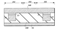
配線基板1は、配線領域101及び半導体素子搭載領域102とを有し、配線領域101に第1主表面(図1中上側)から第2主表面(図1中下側)に通じる接続孔11を有する絶縁性基材10と、接続孔11内において絶縁性基材10の第2主表面に達しないように埋め込まれた埋込導体12と、絶縁性基材10の第1主表面において接続孔11内の埋込導体12に一端が電気的に接続され、他端が半導体素子搭載領域102まで伸延された配線層14とを備えている。図2に示すように、配線領域101は、半導体素子搭載領域102を取り囲むように、平面上配置されている。即ち、配線領域101は配線基板1の周辺部分の領域であり、半導体素子搭載領域102は配線基板1の中央部分の領域である。そして、第1の実施例に係る半導体装置は、半導体素子搭載領域102に半導体素子2を搭載する。即ち、半導体素子2は、半導体素子搭載領域102において、配線層14に接続されている。
The
絶縁性基材10は、絶縁性を有する配線基板1の基材(母材)である。必ずしもこのような形状に限定されるものではないが、図2に示すように、絶縁性基材10の平面形状は、基本的には半導体素子2の平面形状に相似する方形状で構成されている。この絶縁性基材10には例えば絶縁性樹脂を実用的に使用することができる。
The insulating
接続孔11は、その内部に埋設された埋込導体12により、配線基板1の第1主表面の配線層14と、配線基板1の第2主表面側の図示しない他のデバイス例えば別の配線基板1(後述する図19参照。)との間を電気的に接続するための接続孔として少なくとも使用されている。必ずしもこのような形状に限定されるものではないが、図2に示すように、接続孔11の平面形状(開口形状)は円形で構成されている。なお、接続孔11の平面形状としては、矩形(方形)形状、5角形以上の多角形の形状等も使用することができる。更に、接続孔11内において絶縁性基材10の第2主表面に達しないように第1主表面部分に埋込導体12が配設されているので、接続孔11は、その内壁面と、配線基板1の第2主表面から第1主表面側に向かって底上げされた埋込導体12の第1主表面とで凹型形状の空隙部(位置決め部)110を構成するようになっている。この空隙部(位置決め部)110は、配線基板1(第1の配線基板1a)と別の配線基板(第2の配線基板1b)とを多段に積み上げるための位置決め用空間として使用できる(図19参照)。
The
埋込導体12は、配線基板1の第2主表面側に配設される他の配線基板に電気的に接続するための電極(端子)としての機能を備え、かつ配線基板1の配線層14と他の配線基板との間を電気的に接続するための接続孔配線(スルーホール配線又はビア配線)としての機能を備えている。そして、この埋込導体12は、更に配線基板1の第1主表面において配線層14(特に端子部14A)の膜厚を補い機械的強度を高め、配線基板1の第2主表面において他の配線基板と積層するための位置決め部110としての凹部形状を形成するようになっている。即ち、埋込導体12は、基本的には絶縁性基材10の厚さよりも薄い膜厚で形成されており、機械的強度を高める上で配線層14の膜厚よりも厚い膜厚で形成することが好ましい。埋込導体12には、導電性に優れた、例えば50μm〜60μm、好ましくは55μmの膜厚の銅(Cu)薄膜又は適度な添加物を含む銅合金薄膜を使用することができる。
The buried
配線層14は、一端側に膜厚が薄い端子部14A及び端子部14Aから引き出された配線部14Bを有しており、他端側に端子部14A及び配線部14Bに比べて膜厚が厚い突起状の電極部14Cを有している。これらの端子部14A、配線部14B及び電極部14Cは一体として、同一導電性材料で形成されている。端子部14A及び配線部14Bは配線基板1の配線領域101に配設されている。配線領域101は半導体素子搭載領域102まで伸延され、電極部14Cは、この半導体素子搭載領域102に配設されている。端子部14Aは、埋込導体12に電気的に接続されている。配線部14Bは端子部14Aと電極部14Cとの間の電気的な接続を行うようになっている。電極部14Cは、半導体素子(半導体チップ)2の素子形成面側(図1中下側)に配設されたボンディングパッド20との間の電気的な接続を行うようになっている。
The
半導体素子2は、本発明の第1の実施例において、シリコン(Si)単結晶基板(シリコン単結晶チップ)の表面部に、能動素子、受動素子等を集積回路化した半導体チップである。図1においては、この半導体素子(半導体チップ)2は、ベアチップであり、樹脂封止体等で全体的にモールドされていない状態と9して示している。この半導体素子(ベアチップ)2の表面には複数のボンディングパッド20が配設されている。これらの複数のボンディングパッド20は、能動素子、受動素子等からなる集積回路と配線層14の電極部14Cとの間を電気的に接続するために用いられる。
In the first embodiment of the present invention, the
具体的には、複数のボンディングパッド20は、例えば、半導体素子(半導体チップ)2の素子形成面に形成された1×1018cm−3〜1×1021cm−3程度のドナー若しくはアクセプタがドープされた複数の高不純物密度領域(ソース領域/ドレイン領域、若しくはエミッタ領域/コレクタ領域等)等にそれぞれ、接続されている。そして、この複数の高不純物密度領域にオーミック接触するように、アルミニウム(Al)、若しくはアルミニウム合金(Al−Si,Al−Cu−Si)等の金属から成る複数の電極層が形成されている。そしてこの複数の電極層の上部には、酸化膜(SiO2)、PSG膜、BPSG膜、窒化膜(Si3N4)、或いはポリイミド膜等から成るパッシベーション膜が形成されている。そして、パッシベーション膜の一部に複数の電極層を露出するように複数の開口部(窓部)を設け、複数のボンディングパッド20を構成している。或いは、複数の電極層と金属配線で接続された他の金属パターンとして、複数のボンディングパッド20を形成してもかまわない。又、MOSFET等であれば、ポリシリコンゲート電極にアルミニウム(Al)、若しくはアルミニウム合金(Al−Si,Al−Cu−Si)等の金属からなる複数のボンディングパッド20を形成することが可能である。或いは、複数のポリシリコンゲート電極に接続されたゲート配線等の複数の信号線を介して、他の複数のボンディングパッド20を設けても良い。ポリシリコンから成るゲート電極の代わりに、タングステン(W)、チタン(Ti)、モリブデン(Mo)等の高融点金属、これらのシリサイド(WSi2,TiSi2,MoSi2)等、或いはこれらのシリサイドを用いたポリサイド等から成るゲート電極でもかまわない。そして、図1に示すように、半導体素子2は、集積回路が配設された表面部を下側に向けたフェイスダウン(フリップチップ)方式で配線基板1の表面上に取り付けられている(実装されている)。フリップチップ構造の場合は、これらのボンディングパッド20は、必ずしも、半導体素子(半導体チップ)2の周辺部に配置されている必要はない。配線層14には、埋込導体12と同様に、導電性に優れた、最も膜厚が厚い電極部14Cにおいて例えば30μm〜40μm、好ましくは35μmの膜厚の銅薄膜等を使用することができる。
Specifically, the plurality of
図2に示すように、本発明の第1の実施例において、複数の電極部14Cの平面サイズは、ストライプ形状の複数の配線部14Bの幅寸法よりも小さく設定されている。このようにして、この配線基板1は、半導体素子2の多数のボンディングパッド20を、多端子狭ピッチのエリアアレイ型配置する場合に有効である。
As shown in FIG. 2, in the first embodiment of the present invention, the planar size of the plurality of
なお、接続孔11内において埋込導体12と配線層14の端子部14Aとの間には、導電性を有し、少なくとも埋込導体12(及び配線層14)との間に適度なエッチング選択比を有するエッチングストッパ層13が配設されている。
In the
このエッチングストッパ層13には、例えば0.1μm〜0.3μm、好ましくは0.2μmの膜厚のニッケル(Ni)薄膜等を使用することができる。
For the
半導体素子2の取付には、例えば複数のボンディングパッド20と複数の電極部4Cとの間で電気的な導通を行うことができ、それ以外の領域においては絶縁性を確保した状態で接着することができる異方性導電材3が使用されている。異方性導電材3は、ウレタン樹脂やエポキシ樹脂等の絶縁性樹脂の中に、金(Au)、銀(Ag)、ニッケル(Ni)、或いはチタン・ニッケル合金(Ti−Ni)等の金属粉末を分散させた材料より構成されている。異方性導電材3は、応力の印加された場所のみが導電性を有する異方性を有するので、複数の電極部4Cの近傍のみが導電性を有する。
For the mounting of the
以上説明したように、本発明の第1の実施例に係る配線基板1においては、配線層14の配線領域101に位置する端子部14Aの膜厚を接続孔11内に埋め込まれた埋込導体12で補うことができる(見かけ上の膜厚を増加することができる)ので、端子部14Aの機械的強度を高め、この領域における破損、特に基板間接続部6との間の破損を防止することができる。更に、端子部14Aの膜厚は上記のように埋込導体12で補われているので、配線層14の配線領域101に位置する端子部14A並びに配線部14Bの膜厚を薄膜化することができ、端子部14A並びに配線部14B等の微細化又は配線部14Bの多端子化を実現することができる。
As described above, in the
更に、本発明の第1の実施例に係る配線基板1において、配線層14の一端側(配線領域101)に膜厚が薄い端子部14A並びに配線部14Bを備えたので、端子部14A並びに配線部14Bの狭ピッチ化及び端子部14Aの多端子化を実現することができ、配線基板1の小型化を実現することができる。更に、配線層14の他端側(半導体素子搭載領域102)の膜厚を厚くした電極部14Cを備えたので、電極部14Cに例えば半導体素子(ベアチップ)2のボンディングパッド20をフェイスダウンボンディング方式により直接的に接続することができる。即ち、電極部14Cとボンディングパッド20との間の電気的な接続に、半導体素子2の表面、側面及び裏面に沿って迂回するような接続経路をなくすことができるので、半導体素子2のサイズの範囲内で双方の接続が行え、配線基板1の小型化を実現することができる。
Furthermore, in the
更に、本発明の第1の実施例に係る半導体装置においては、上記配線基板1で得られる効果と同様に、配線基板1の配線層14の配線領域101に位置する端子部14Aの破損を防止することができ、配線層14の配線領域101の膜厚を薄膜化して端子部14A、配線部14B等の微細化又は端子部14Aの多端子化を実現することができ、複雑な構造にすることなく位置決め部110を形成することができる。従って、図19に示すような三次元実装構造に好適な半導体装置を実現することができる。図19は、本発明の三次元実装構造を有する半導体装置の概略を示す模式的な断面図で、図1に示す半導体装置を、基板間接続部材6を介して積層した構造に対応する。
Furthermore, in the semiconductor device according to the first embodiment of the present invention, the damage to the
即ち、図19において、下層の第1の配線基板1aは、配線領域101a及び半導体素子搭載領域102aとを有し、配線領域101aに第1主表面から第2主表面に通じる第1の接続孔11aを有する第1の絶縁性基材10aと、第1の接続孔11a内に埋め込まれた第1の埋込導体12aと、第1の絶縁性基材10aの第1主表面において第1の埋込導体12aに一端が電気的に接続され、他端が半導体素子搭載領域102aまで配設された第1の配線層14aとを備えている。そして、下層の第1の半導体素子2aは、第1の配線層14aの半導体素子搭載領域102aに接続されている。
That is, in FIG. 19, the first wiring substrate 1a in the lower layer has a wiring region 101a and a semiconductor element mounting region 102a, and a first connection hole that leads from the first main surface to the second main surface in the wiring region 101a. A first insulating
そして、第1の配線基板1aの配線領域101aには、基板間接続部材6が配置され、この基板間接続部材6に、第2の配線基板1bの第2の埋込導体12bが電気的に接続されている。基板間接続部材6としては、半田ボール、金(Au)バンプ、銀(Ag)バンプ、銅(Cu)バンプ、ニッケル/金(Ni−Au)バンプ、或いはニッケル/金/インジウム(Ni−Au−In)バンプ等が使用可能である。半田ボールとしては、直径100μm乃至250μm、高さ50μm乃至200μmの錫(Sn):鉛(Pb)=6:4の共晶半田等が使用可能である。或いは、Sn:Pb=5:95等他の組成の半田でも良い。
An
この上層の第2の配線基板1bは、下層の第1の配線基板1aと基本的に同一構造である。即ち、第2の配線基板1bも、配線領域101b及び半導体素子搭載領域102bとを有している。そして、第2の絶縁性基材10bの配線領域101bにおいて、第1主表面から第2主表面に通じる第2の接続孔11bが形成されている。この第2の接続孔11b内には、第2の埋込導体12bが埋め込まれている。製造工程を、後述するが、第2の接続孔11bの底部近傍の空隙部が、位置決め部110bとなり、この位置決め部110bの内部に、基板間接続部材6が入り込むので、自動的に上下の第1の配線基板1aと第2の配線基板1b間の位置決めを行うことができる。第2の埋込導体12bは、第2の絶縁性基材10bの第1主表面において第2の配線層14bに接続されている。この第2の配線層14bの他端は、半導体素子搭載領域102bまで延長形成されている。そして、第2の半導体素子2bは、第2の配線層14bの半導体素子搭載領域102bに形成された電極部4Cにおいて、第2の配線層14bに接続されている。
The upper second wiring board 1b basically has the same structure as the lower first wiring board 1a. That is, the second wiring board 1b also has a wiring region 101b and a semiconductor element mounting region 102b. And in the wiring area | region 101b of the 2nd insulating base material 10b, the 2nd connection hole 11b leading from a 1st main surface to a 2nd main surface is formed. A second embedded conductor 12b is embedded in the second connection hole 11b. Although the manufacturing process will be described later, the gap portion near the bottom of the second connection hole 11b becomes the positioning portion 110b, and the
第1の半導体素子2a及び第2の半導体素子2bの取付には、それぞれのボンディングパッド20a、20bと第1の配線層14a,第2の配線層14bとの間で電気的な導通を行うことができる異方性導電材3a,3bが使用されている。
For the attachment of the
図19は、2枚の第1の配線基板1a,第2の配線基板1bを積層した構造を、例示したが、更に、第3の配線基板,・・・・・等を多段に積み上げた三次元実装構造の半導体装置を構成できることは勿論である。このように、本発明の第1の実施例に係る半導体装置によれば、基板間接続部材6を用いることにより、それぞれ第1の半導体素子2a,第2の半導体素子2b,第3の半導体素子・・・・・を有する複数の(多数の)第1の配線基板1a,第2の配線基板1b,第3の配線基板・・・・・を基板間接続部材6により基板厚さ方向に複数積層をすることができるので、高実装密度化を図ることができる三次元実装構造を実現することができる。又、図19に示すような、三次元実装構造の構築に必要な位置決め部110(110b)を、接続孔11(11b)を利用し、接続孔11内の表面部分にのみ埋込導体12を配設し、第2主表面側には埋込導体12(12b)の空隙部を設けることにより生成した凹部で形成することができる。従って、特に部品点数を増加することなく、又、複雑な構造にすることなく、位置決め部110(110b)を形成することができる。
FIG. 19 exemplifies the structure in which the two first wiring boards 1a and the second wiring board 1b are stacked. Further, the third wiring board,... Of course, a semiconductor device having an original mounting structure can be configured. As described above, according to the semiconductor device of the first embodiment of the present invention, by using the
[配線基板1の製造方法]
次に、本発明の第1の実施例に係る配線基板1の製造方法を、図3乃至図15を使用して説明する。
[Manufacturing method of wiring board 1]
Next, a method for manufacturing the
(イ)図3に示すように、配線領域101及びこの配線領域101とは異なる半導体素子搭載領域102を含む範囲において、裏面導体層120上にエッチングストッパ層13を介在させて表面導体層140を形成し、裏面導体層120、エッチングストッパ層13及び表面導体層140の3層の金属積層体を準備する。裏面導体層120は埋込導体12を形成するためのものであり、この裏面導体層120には例えば、50μm〜80μm、好ましくは65μm程度の膜厚の銅薄膜等を使用することができる。表面導体層140は配線層14、即ち端子部14A、配線部14B及び電極部14Cを形成するためのものであり、表面導体層140には例えば、30μm〜40μm、好ましくは35μmの膜厚の銅薄膜等を使用することができる。そして、このエッチングストッパ層13には、例えば0.1μm〜0.3μm、好ましくは0.2μmの膜厚のニッケル(Ni)薄膜を使用すれば良い。
(A) As shown in FIG. 3, in a range including the
(ロ)裏面導体層120の表面(図3中、裏面導体層120の下面)上にレジスト膜が塗布され、このレジスト膜に露光処理及び現像処理を行い、レジスト膜でエッチングマスク(図示しない。)が作成される。このエッチングマスクは、ポジティブタイプのレジスト膜の場合、裏面導体層120の配線領域101の接続孔11の形成予定領域を覆うようになっており、それ以外の領域は覆われていない。このレジスト膜からなるエッチングマスクを使用し、半導体素子搭載領域102において裏面導体層120をエッチングにより取り除き、図4に示すように配線領域101において残存する裏面導体層120から複数の柱状(突起状)の埋込導体(突起電極)12を形成する。この埋込導体12の形成に際して、裏面導体層120の半導体素子搭載領域102のエッチング量はエッチングストッパ層13により制御され、エッチングストッパ層13との界面において裏面導体層120の半導体素子搭載領域102を確実に取り除くことができる。埋込導体12の形成後、エッチングマスクを除去する(レジスト膜が剥離される)。
(B) A resist film is applied on the surface of the back conductor layer 120 (the lower surface of the
(ハ)埋込導体12をエッチングマスクとして使用し、図5に示すようにエッチングストッパ層13の半導体素子搭載領域102をエッチングにより取り除く。エッチングストッパ層13は、表面導体層140との間にエッチング選択比を有しているので、表面導体層140側にオーバエッチングすることなく、選択的に除去することができる。エッチングストッパ層13を除去した後に、粗化処理が行われる。この粗化処理においては、粗化処理液として例えば三菱ガス化学社製、商品名CPE−900を使用することができる。
(C) Using the embedded
(ニ)図6に示すように、埋込導体12側において、配線領域101及び半導体素子搭載領域102を含む範囲の絶縁性基材100及び平坦化部材16を準備する。絶縁性基材100には、例えばガラスフィラー不織布にエポキシ樹脂が含芯された日立化成工業株式会社製、商品名E679−P等の絶縁性樹脂を使用することができる。絶縁性基材100は、埋込導体12の膜厚よりも厚いものが使用され、その厚さは、例えば、51μm〜130μm程度に選ぶ。つまり、この絶縁性基材100の厚さは、埋込導体12の底部から絶縁性基材100の第2主表面との距離が1μm以上50μm以下であるように選ぶことが好ましい。又、平坦化部材16には、例えば18μmの膜厚を有する銅箔を実用的に使用することができ、この銅箔は粗化されていないシャイニー面と呼ばれる平滑な面を備えている。この平坦化部材16のシャイニー面が絶縁性基材100の表面に接触するように、平坦化部材16が取り付けられる。
(D) As shown in FIG. 6, the insulating
(ホ)埋込導体12と平坦化部材16との間に絶縁性基材100を介在させ、図7に示すように平坦化部材16により埋込導体12側に絶縁性基材100を加圧する。この加圧により、平坦化部材16で絶縁性基材100の表面(図7中、下側表面)の平坦性が確保されつつ、埋込導体12上の絶縁性基材100の一部を周囲に押し出すことができる。このため、埋込導体12の周囲(半導体素子搭載領域102)を、絶縁性樹脂で覆うように絶縁性基材100を形成することができる。平坦化部材16のシャイニー面を絶縁性基材100の表面に接触させているので、埋込導体12上の絶縁性基材100は周囲にスムースに押し出すことができる。
(E) The insulating
(ヘ)この後、図8に示すように、平坦化部材16を取り除く。前述のように平坦化部材16のシャイニー面を絶縁性基材100の表面に接触させていたので、絶縁性基材100の表面から平坦化部材16をスムースに剥離することができる。図9は平坦化部材16を完全に取り除いた状態の絶縁性基材100を示している。即ち、図9においては、表面導体層140の裏面に接した第1主表面及びこの第1主表面に対向した第2主表面とを有し、埋込導体12の側壁に接して形成された絶縁性基材100が示されている。絶縁性基材100は、更に、埋込導体12の底面に接して形成されている。この結果、前述したように、底面と絶縁性基材100の第2主表面との距離tが、1μm以上50μm以下となる。1μm以上50μm以下の厚さに選定することにより、以下で説明する研磨工程等が容易になる。
(F) Thereafter, as shown in FIG. 8, the planarizing
(ト)図10に示すように、埋込導体12の表面が露出するまで絶縁性基材100の表面を研磨し、絶縁性基材100の絶縁性樹脂及びこの絶縁性樹脂に充填されたフィラーを取り除き、この研磨された絶縁性基材100から、埋込導体12の周囲を覆う絶縁性基材10を表面導体層140に形成することができる。
(G) As shown in FIG. 10, the surface of the insulating
研磨は例えば以下のように行われる。まず、表面導体層140側に低温で溶融固化する接着材を塗布し、この接着材を固化した面を定盤に固定する。この定盤に対して平行度の高い回転盤上に研磨剤を所定量注入し、定盤を回転盤に向かって降下させる。14.7kPaの荷重を掛けた状態で回転盤を回転させ、約15分間、研磨を行う。このような条件下で埋込導体12の表面を露出させることができる。この結果、絶縁性基材10は、埋込導体12の底面を露出している。
For example, the polishing is performed as follows. First, an adhesive that melts and solidifies at a low temperature is applied to the
(チ)その後、表面導体層140の表面(図11中、表面導体層140の上面)上にレジスト膜を塗布する。このレジスト膜に露光処理及び現像処理を行い、図11に示すようにレジスト膜からなるエッチングマスク145が作成される。このエッチングマスク145は、表面導体層140の半導体素子搭載領域102の電極部14Cの形成予定領域を覆うようになっており、それ以外の領域は覆われていない。レジスト膜には、例えば日立化成工業株式会社製、商品名レジストHi―RC、日本合成化学工業株式会社製、商品名レジスト401y25等を使用することができる。後者の401y25の場合においては、ロール温度110℃、ロール速度0.6m/minの条件でレジスト膜が塗布(ラミネート)される。露光処理においては、積算露光量約80mJ/cm2の露光条件で電極部14Cのパターン像が焼き付けられる。現像処理においては、炭酸ナトリウム溶液、又は水酸化テトラメチルアンモニウム溶液で現像が行われる。現像処理が終了した後には、エッチングマスク145に100mJ/cm2〜300mJ/cm2の露光量で後露光が行われ、エッチングマスク145の密着性を確実なものにすることができる。
(H) Thereafter, a resist film is applied on the surface of the surface conductor layer 140 (the upper surface of the
(リ)このエッチングマスク145を使用し、表面導体層140の配線領域101を選択的に薄くするためのハーフエッチングを行う。これにより、図12に示すように、局部的に膜厚を薄くされた表面導体層141が、形成され、エッチングマスク145で覆われた表面導体層140の残留部分には膜厚が厚い電極部14Cが形成される。即ち、電極部14Cは表面導体層140の膜厚がそのまま引き継がれて、例えば35μmの厚い膜厚で形成され、選択的なハーフエッチングが行われた表面導体層141は、例えば10μm〜15μm程度の膜厚に薄くなる。ここで、埋込導体12の裏面(底部)上にはエッチングマスクが形成されていない。即ち、埋込導体12の裏面(底部)は、絶縁性基材10から露出した状態になっており、絶縁性基材10をエッチングマスクとして使用し、埋込導体12の膜厚方向の一部がエッチングにより同時に取り除かれる。この埋込導体12の裏面(底部)のエッチングにより、埋込導体12は接続孔11内において底上げされ、この接続孔11の内壁面と埋込導体12の裏面(底部)とで生成される凹形状の位置決め部110を形成することができる。上記ハーフエッチングには、例えば主成分が硫酸、過酸化水素からなる溶液がエッチング液として使用される。詳細には、三菱ガス化学社製化学研磨液、商品名SE−07、商品名CPE−750、商品名CPS、又はそれらの混合液をエッチング液として使用することができる。エッチング液の過酸化水素濃度は2.0g〜10.0g/100ml、銅濃度は3.0g〜10.0g/100mlに調整し、コンベアエッチング装置のシャワーリングにより液温度20℃〜35℃の範囲でハーフエッチングが行われる。ハーフエッチングの後、エッチングマスク145は除去される。このエッチングマスク145の除去は水酸化ナトリウム溶液、又は水酸化カリウム溶液で行われる。
(I) Using this
(ヌ)そして、図13に示すように、表面側(図13中上側)において表面導体層141上にレジスト膜がラミネートされ、裏面側(図13中下側)においてレジスト膜147がラミネートされる。これらのレジスト膜は、表面側及び裏面側において同時にラミネートしても良く、又、別々にラミネートしても良い。表面側にラミネートされたレジスト膜に、所定のマスクを用いて、露光処理及び現像処理を行う。この結果、図13に示すように、表面側のレジスト膜からなるエッチングマスク146が作成される。このエッチングマスク146は、図2に示すように、表面導体層141の配線領域101に位置する端子部14A、及びストライプ形状の配線部14Bの形成予定領域と電極部14Cとを覆うような、特定のパターンになっており、それ以外の領域は覆われていない。裏面側にラミネートされたレジスト膜147にも同様に露光処理及び現像処理を行い、図13に示すように裏面側全面が覆われたエッチングマスク147が作成される。レジスト膜には、例えば日立化成工業株式会社製、商品名レジストHi―RC、日本合成化学工業株式会社製、商品名レジスト401y25等を使用することができる。レジスト膜は例えば110℃のロール温度でラミネートすることができる。ラミネート速度は、電極部14Cを形成したエッチングマスク145のレジスト膜のラミネート速度よりも遅く、例えば0.3m/minに設定され、膜厚が薄い表面導体層141と膜厚が厚い電極部14Cとの境界の段差部における気泡の巻き込みを減少させることができる。露光処理においては、積算露光量約80mJ/cm2の露光条件で端子部14A、配線部14B及び電極部14Cのパターン像が焼き付けられる。現像処理においては、炭酸ナトリウム溶液、又は水酸化テトラメチルアンモニウム溶液で現像が行われる。
(N) Then, as shown in FIG. 13, a resist film is laminated on the
(ル)その後、エッチングマスク146及び147を使用し、表面導体層141を、選択的にエッチングする。この結果、図14に示すように、エッチングマスク146以外の表面導体層141を取り除かれ、複数の端子部14A及び複数のストライプ形状の配線部14Bが形成される。この複数の端子部14A及び複数の配線部14Bを形成することにより、図2に示す平面形状のような、複数の端子部14A、複数の配線部14B及び複数の電極部14Cを有する配線層14を形成することができる。エッチングには、塩化第二鉄、塩化第二銅を主成分とするエッチング液、若しくはアルカリエッチング液、例えばメルストリップ社製、商品名Aプロセス液を使用することができる。
(L) Then, using the etching masks 146 and 147, the
(ヲ)その後、図14に示すように、エッチングマスク146及び147が除去される。この除去には水酸化ナトリウム溶液、又は水酸化カリウム溶液を使用することができる。なお、エッチングマスク146及び147の除去後には、埋込導体12及び配線層14以外の露出表面上にソルダーレジスト膜を形成することが好ましい。ソルダーレジスト膜は、特に配線層14の配線部14Bの断線不良を防止することができ、又、後工程でめっき処理を行う場合には、めっき面積を減少することができる。ソルダーレジスト膜には、例えば、四国化成製、商品名レジストFCハードを実用的に使用することができ、レジストFCハードはスクリーン印刷で印刷された後に熱硬化させることでソルダーレジスト膜を形成することができる(本発明の第1の実施例に係る配線基板1においては、ソルダーレジスト膜は形成していない。)。
(E) Thereafter, as shown in FIG. 14, the etching masks 146 and 147 are removed. For this removal, a sodium hydroxide solution or a potassium hydroxide solution can be used. Note that, after removing the etching masks 146 and 147, it is preferable to form a solder resist film on the exposed surface other than the buried
(カ)そして、図15に示すように、埋込導体12の表面上、配線層14の端子部14A上、配線部14B上及び電極部14C上にめっき層15を形成する。めっき層15にはニッケル(Ni)めっき、金(Au)めっき等を実用的に使用することができ、めっき層15は例えば無電解めっき法又は電解めっき法により形成することができる。
(F) Then, as shown in FIG. 15, the
ここまでの工程が終了した段階で、本発明の第1の実施例に係る配線基板1を完成させることができる。
When the steps so far are completed, the
上記のような本発明の第1の実施例に係る配線基板1の製造方法においては、埋込導体12の一部を選択的に薄くする工程と、表面導体層140の配線領域101の一部を膜厚方向に除去して端子部14A並びに配線部14Bを形成する工程と、表面導体層140の半導体素子搭載領域102に電極部14Cを形成する工程(端子部14A並びに配線部14Bを有する配線層14を形成する工程)とを同一工程で行うことができる。従って、配線基板1の製造工程数を削減することができる。この配線基板1の製造工程数の削減に伴い、製造上の歩留まりを向上することができ、又、生産コスト、製品コスト等を減少することができる。更に、本発明の第1の実施例に係る配線基板1の製造方法においては、埋込導体12の周囲を被覆する絶縁性基材10をマスクとして埋込導体12の一部を膜厚方向に除去することができるので、このマスク(配線基板1の裏面側に形成される例えばレジスト膜)を形成する工程に相当する分、配線基板1の製造工程数を削減することができる。
In the method of manufacturing the
更に、本発明の第1の実施例に係る配線基板1の製造方法においては、裏面導体層120と表面導体層140との間にエッチングストッパ層13を介在させることにより、裏面導体層120、表面導体層140のそれぞれを適正な膜厚で独立にパターニングすることができる。具体的には、微細化又は多端子化を実現するために配線層14の膜厚は薄く設定され、膜厚を稼ぐために埋込導体12の膜厚は厚く設定されるが、エッチングストッパ層13を介在させることで、表面導体層140の膜厚を損なうことなく、裏面導体層120をパターニングして突起状の埋込導体12を形成することができる。
Furthermore, in the method of manufacturing the
[半導体装置の製造方法]
次に、本発明の第1の実施例に係る半導体装置の製造方法(組立方法)を、図1、図2、図16及び図17を使用して説明する。
[Method for Manufacturing Semiconductor Device]
Next, a semiconductor device manufacturing method (assembly method) according to a first embodiment of the present invention will be described with reference to FIGS. 1, 2, 16, and 17. FIG.
(イ)まず配線基板1の表面上の半導体素子搭載領域102に異方性導電材3を配置し、所定の加熱温度において所定荷重を加えた状態で一定の時間圧着することにより、図16に示すように異方性導電材3を仮圧着させることができる。
(A) First, the anisotropic
異方性導電材3には、例えば日立化成工業株式会社製の異方性導電フィルムを使用することができる。
As the anisotropic
(ロ)異方性導電材3上に半導体素子2を配置し、図17に示すように配線基板1の電極部14Cと半導体素子2のボンディングパッド20との間の位置合わせ(アライメント)を行う。本発明の第1の実施例において、半導体素子2にはベアチップが使用されているので、半導体素子2のボンディングパッド20が直接的に配線基板1の電極部14Cに接続できるように、半導体素子2はフェイスダウン(フリップチップ)方式で配置される。半導体素子2のアライメントターゲットは、半導体素子2の輪郭形状をそのまま使用することができる。一方、配線基板1においては、図示していないが、例えば端子部14A及び配線部14Bの形成工程と同一工程で表面導体層141を利用してアライメントターゲットを形成することができる。表面導体層141は薄い膜厚で形成されているので、アライメントターゲットの加工精度を向上することができる。
(B) The
(ハ)位置合わせ後に、所定の加熱温度において所定荷重を加えた状態で一定の時間、配線基板1に半導体素子2を押し付け、半導体素子2を配線基板1に仮固定する。その後、本固定を行い、前述の図1及び図2に示す半導体装置を完成させることができる。配線基板1の電極部14Cと半導体素子2のボンディングパッド20との間は異方性導電材3を通して良好な電気的接続状態を確保することができる。更に、半導体素子2自体は配線基板1の表面に異方性導電材3を介在させて機械的に強固に取り付けられる。なお、仮固定を行わずに、半導体素子2を配線基板1に直接的に本固定することができる。
(C) After alignment, the
[三次元実装構造を有する半導体装置の製造方法]
次に、本発明の第1の実施例に係る三次元実装構造を有する半導体装置の製造方法を、図18及び図19を使用して各々説明する。
[Method of manufacturing a semiconductor device having a three-dimensional mounting structure]
Next, a method for manufacturing a semiconductor device having a three-dimensional mounting structure according to the first embodiment of the present invention will be described with reference to FIGS.
(イ)まず、図18に示すように配線基板(第1の配線基板)1aの端子部14A上に基板間接続部材6を形成する。本発明の第1の実施例において、基板間接続部材6には半田ボールを使用することができる。この半田ボールは、例えば日立ビアメカニクス株式会社製の半田ボール搭載機を使用することにより簡易に形成することができる。
(A) First, as shown in FIG. 18, the
(ロ)そして、図19に示すように、第1の配線基板1a上に同様の製造プロセスで形成した同一構造の他の配線基板(第2の配線基板)1bを多段に積み上げる。第1の配線基板1aの端子部14A上の基板間接続部材6の上部は他の(第2の)配線基板1bの裏面側の位置決め部110b内部に入り込み、自動的に上下の第1の配線基板1aと第2の配線基板1b間の位置決めを行うことができる。そして、図19に示すように、半田リフローを行い、第1の配線基板1aの端子部14Aと基板間接続部材6との間を電気的かつ機械的に接合するとともに、上層に積み上げられた第2の配線基板1bの位置決め部110bから露出する第2の埋込導体12bと基板間接続部材6との間を電気的かつ機械的に接合する。この半田リフローは、例えば、多段に積み上げられた第1の配線基板1aと第2の配線基板1bをコンベア搬送により赤外線リフロー装置内を通過させることで行うことができ、赤外線リフロー装置の加熱温度とコンベア搬送の搬送速度とにより半田リフロー条件を設定することができる。この半田リフローが終了した段階で第1の配線基板1a,第2の配線基板1b,第3の配線基板・・・・・を多段に積み上げた三次元実装構造の半導体装置を完成させることができる。
(B) Then, as shown in FIG. 19, other wiring boards (second wiring boards) 1b having the same structure formed by the same manufacturing process are stacked on the first wiring board 1a in multiple stages. The upper part of the
図20は、本発明の第1の実施例の変形例に係る半導体装置の断面図である。図20に示すように、配線基板1の電極部14Cに、パッケージ化された半導体素子21が取り付けられている。必ずしもこの構造に限定されるものではないが、半導体素子21は、リードレスチップキャリア(LCC)構造で構成されており、ベアチップをレジンモールドしたものである。半導体素子21のアウターリードはレジンモールド部に沿って成型されている。なお、詳細な構造は示していないが、ベアチップはフェイスアップボンディング方式でインナーリード上に取り付けられている。
FIG. 20 is a sectional view of a semiconductor device according to a modification of the first embodiment of the present invention. As shown in FIG. 20, a packaged
このような半導体素子21が取り付けられた配線基板1は、前述の図19に示す半導体装置と同様に、多段に積み上げられ、三次元実装構造を構築するようになっている。
The
なお、三次元実装構造の半導体装置は、同一の半導体素子2、又は同一の半導体素子21を多段に積み上げる方式に限定されるものではなく、半導体素子2を取り付けた配線基板1と半導体素子21を取り付けた配線基板1とを多段に積み上げても良い。又、半導体素子21はTAB構造であっても良い。
Note that the semiconductor device having a three-dimensional mounting structure is not limited to a method in which the
(第2の実施例)
本発明の第2の実施例は、本発明の第1の実施例に係る配線基板1の電極部14Cの形状を代えた例を説明するものである。図21に示す配線基板1の平面図は、前述の本発明の第1の実施例に係る配線基板1の製造方法の図13に示す工程に対応する工程における平面図である。
(Second embodiment)
The second embodiment of the present invention describes an example in which the shape of the
即ち、複数の電極部14Cが連結した状態で形成された後に、1つの端子部14A及び1つの配線部14Bをパターニングするためのエッチングマスク146が電極部14Cと交差した形状で形成されている。このエッチングマスク146を使用して表面導体層141をパターニングすることにより、端子部14A及び配線部14Bが形成されるとともに複数の電極部14Cが個々に分割されるようになっている。
That is, after the plurality of
このように形成される配線基板1の電極部14Cは配線部14Bと同等の幅寸法で形成され、半導体素子2のボンディングパッド20が少ピン広ピッチのペリフェラル配置に有効な配線基板1を形成することができる。
The
(第3の実施例)
本発明の第3の実施例は、図22に示すように、配線基板1上に複数の半導体素子2を取り付けたMCM構造の半導体装置としたことである。複数の半導体素子2は、メモリデバイスのように同一のものであっても良いし、メモリデバイスとロジックデバイスとが混在するようなものであっても良い。
(Third embodiment)
The third embodiment of the present invention is that the semiconductor device has an MCM structure in which a plurality of
更に、図22に示す構造の複数の配線基板1a,ab,・・・・・を多段に積み上げて、前述の図19と同様な、三次元実装構造としても良い。 Furthermore, a plurality of wiring boards 1a, ab,... Having the structure shown in FIG. 22 may be stacked in multiple stages to form a three-dimensional mounting structure similar to that shown in FIG.
(第1の参考例)
本発明の第1の参考例に係る半導体装置は、図23に示すように、配線領域101及び半導体素子搭載領域102を有する絶縁性基材10と、配線領域101において、絶縁性基材の第1主表面から第2主表面に通じる接続孔11と、絶縁性基材10の第1主表面において、接続孔11に一端が接続され、他端が半導体素子搭載領域102まで伸延された配線層14と、半導体素子搭載領域102において、配線層14に接続された半導体素子2とから構成されている。しかし、第1の実施例とは異なり、接続孔11の内部には、埋込導体は存在しない。即ち、埋込導体を用いる代わりに、接続孔11内に露出した配線層14の裏面に選択的に形成された金属薄膜15を更に備えている。金属薄膜15は、例えば、厚さ5〜30μmのニッケルめっき層、及びこのニッケルめっき層の上に形成された厚さ2〜10μmの金めっき層等で構成すれば良い。
(First reference example)
As shown in FIG. 23, the semiconductor device according to the first reference example of the present invention includes an insulating
本発明の第1の参考例においては、接続孔11内に、大きな空隙部110が存在する。従って、この大きな空隙部110を、三次元実装構造に必要な位置決め部として利用できる。つまり、特に部品点数を増加することなく、又、複雑な構造にすることなく位置決め部を形成することができる。従って、前述の図19に示すように、複数の配線基板1a,ab,・・・・・を多段に積み上げて三次元実装構造とするのが容易であるという利点を有する。
In the first reference example of the present invention, a
(第4の実施例)
本発明の第4の実施例に係る半導体装置は、図24に示すように、配線領域101及び半導体素子搭載領域102を有する絶縁性基材10と、配線領域101において、絶縁性基材10の第1主表面から第2主表面に貫通して設けられた埋込導体12と、絶縁性基材10の第1主表面において、埋込導体12に一端が電気的に接続され、他端が半導体素子搭載領域102まで伸延された配線層14と、半導体素子搭載領域102において、配線層14に接続された半導体素子2とを備えている。埋込導体12と配線層14の端子部14Aとの間には、エッチングストッパ層13が配設されている。このエッチングストッパ層13は、導電性を有し、埋込導体12及び配線層14に対して、適度なエッチング選択比を有する。例えば、埋込導体12及び配線層14を銅(Cu)とし、エッチングストッパ層13をニッケル(Ni)とすれば、所望の選択比が得られる。埋込導体12の底面には、更に金属薄膜15を備えている。金属薄膜15は、例えば、ニッケルめっき層、及びこのニッケルめっき層の上に形成された金めっき層からなる複合膜等で構成すれば良い。そして、絶縁性基材10の第2主表面と金属薄膜15の底面とは同一平面レベルである。
(Fourth embodiment)
As shown in FIG. 24, the semiconductor device according to the fourth embodiment of the present invention includes an insulating
このような、絶縁性基材10の第2主表面と金属薄膜15の底面とが同一平面レベルである構造であっても、第1の実施例と同様に、端子の微細化及び多端子化が容易にする効果を奏することが可能である。従って、装置の小型化を実現することができ、かつ三次元実装構造にも好適な構造の半導体装置を提供することができる。
Even in such a structure in which the second main surface of the insulating
(第2の参考例)
図25は、本発明の第2の参考例に係る半導体装置の断面図である。第2の参考例においては、図25に示すように、配線領域101及び半導体素子搭載領域102を有する絶縁性基材10と、配線領域101において、絶縁性基材10の第1主表面から第2主表面に貫通して設けられた埋込導体12と、絶縁性基材10の第1主表面において、埋込導体12に一端が電気的に接続され、他端が半導体素子搭載領域102まで伸延された配線層14と、半導体素子搭載領域102において、配線層14に接続された半導体素子2とを備えている。図24とは異なり、絶縁性基材10の第2主表面と埋込導体12の底面とが同一平面レベルである。そして、埋込導体12の底面には、更に金属薄膜15を備えている。即ち、ニッケル/金めっき層等の金属薄膜15の厚さ分だけ、絶縁性基材10の第2主表面から突出している。
(Second reference example)
FIG. 25 is a cross-sectional view of a semiconductor device according to a second reference example of the present invention. In the second reference example , as shown in FIG. 25, the insulating
(第3の参考例)
更に、本発明の第4の実施例に係る半導体装置において、絶縁性基材10の第2主表面に対して、埋込導体12の底面が突出していてもかまわない。図27は、第3の参考例に係る半導体装置の断面図で、図26は、この半導体装置に用いる配線基板の断面図である。図26においては、表面導体層140と、この表面導体層140の裏面において、この表面導体層140に電気的に接続された複数の埋込導体12と、表面導体層140の裏面に接した第1主表面及びこの第1主表面に対向した第2主表面とを有し、埋込導体12の側壁に接して形成された絶縁性基材10とを備えている。埋込導体12とエッチングストッパ層13とを合計した厚さよりも、絶縁性基材10の方が薄く、埋込導体12の底面が、絶縁性基材10の第2主表面に対して、突出している。例えば、埋込導体12とエッチングストッパ層13とを合計した厚さを50μm〜80μm、好ましくは65μm程度に選び、絶縁性基材10の厚さを30μm〜60μm程度に選べば、図26の構造は容易に構成できる。
(Third reference example)
Furthermore, in the semiconductor device according to the fourth embodiment of the present invention, the bottom surface of the embedded
図27は、図26の表面導体層140を更にパターニングし、端子部14A、配線部14B及び電極部14Cからなる配線層14を形成し、その上に半導体素子2を搭載した構造を示した。即ち、図27に示す半導体装置は、配線領域101及び半導体素子搭載領域102を有する絶縁性基材10と、配線領域101において、絶縁性基材10の第1主表面から第2主表面に貫通して設けられた埋込導体12と、絶縁性基材10の第1主表面において、埋込導体12に一端が電気的に接続され、他端が半導体素子搭載領域102まで伸延された配線層14と、半導体素子搭載領域102において、配線層14に接続された半導体素子2とを備えている。埋込導体12の底面には、更に金属薄膜15を備えている。
FIG. 27 shows a structure in which the
本発明の第4の実施例に係る半導体装置は、前述の図19に示すように、複数の配線基板1a,ab,・・・・・を多段に積み上げて三次元実装構造としても良いことは勿論である。 The semiconductor device according to the fourth embodiment of the present invention may have a three-dimensional mounting structure by stacking a plurality of wiring boards 1a, ab,... Of course.
(その他の実施例)
本発明は上記複数の実施例及び参考例によって記載したが、この開示の一部をなす論述及び図面はこの発明を限定するものであると理解すべきではない。この開示から当業者には様々な代替実施の形態、実施例及び運用技術が明らかとなろう。
(Other examples)
The present invention has been described by the plurality of examples and reference examples, the description and drawings which constitute part of this disclosure should not be understood as limiting the invention. From this disclosure, various alternative embodiments, examples and operational techniques will be apparent to those skilled in the art.
例えば、上記第1乃至第4の実施例の説明においては、接続孔や埋込導体が、配線領域に配置されている場合について説明したが、これらは例示であって、本発明の接続孔や埋込導体は、半導体素子搭載領域に配置されていてもかまわない。 For example, in the description of the first to fourth embodiments, the case where the connection hole and the embedded conductor are arranged in the wiring region has been described. However, these are examples, and the connection hole and The buried conductor may be disposed in the semiconductor element mounting region.
また、前述の図18及び19に示す三次元実装構造の半導体装置において、基板間接続部材6には半田ペーストを使用することができる。半田ペーストはスクリーン印刷法により形成される。スクリーン印刷法においては、予め半導体素子2を配線基板1に取り付けてしまうと、スクリーン印刷マスクが半導体素子2に接触してしまい、端子部14Cとスクリーン印刷マスクとの間に半田ペーストの形成に必要なギャップを確保することができないので、半田ペーストは半導体素子2を取り付ける前に形成しておくことが好ましい。更に基板間接続部材6に、前述の図1に示す異方性導電材3と同等の異方性導電材(例えば異方性導電フィルム)を使用することができる。
In the semiconductor device having the three-dimensional mounting structure shown in FIGS. 18 and 19 described above, a solder paste can be used for the
又、図1、図17〜20、図22〜25、或いは図27においては、集積回路が配設された表面部を下側に向けたフェイスダウン(フリップチップ)方式で配線基板1の表面上に搭載した構造を例示した。しかし、本発明は、フリップチップ実装方式に限定されものではなく、図28に示すように、ボンディングワイヤ25を用いて、半導体素子(半導体チップ)2の周辺部に配置されたボンディングパッド20と、配線層14の電極部14Cとを接続してもかまわない。半導体チップ2と配線層14の電極部14Cとは、保護樹脂31によりモールドされている。更に、ワイヤボンディング方式以外にも、TABテープを用いた接続方式でもかまわない。
In FIGS. 1, 17 to 20, 22 to 25, or 27, the surface of the
更に、本発明は、第1の実施例等では、シリコン(Si)単結晶基板(シリコン単結晶チップ)を用いた集積回路で説明したが、ガリウム砒素(GaAs)等の化合物半導体の集積回路等でもかまわない。 Further, in the first embodiment , the present invention has been described with an integrated circuit using a silicon (Si) single crystal substrate (silicon single crystal chip), but an integrated circuit of a compound semiconductor such as gallium arsenide (GaAs) or the like. But it doesn't matter.
更に、上記実施例に係る配線基板1をプリント配線基板、集積回路用基板、液晶表示装置用基板(例えば透明ガラス基板)等としても良い。
Furthermore, the
又、本発明は、配線基板1の埋込導体12と配線層14とを別々の金属材料で形成しても良い。
In the present invention, the embedded
このように、本発明はここでは記載していない様々な実施の形態等を含むことは勿論である。従って、本発明の技術的範囲は上記の説明から妥当な特許請求の範囲に係る発明特定事項によってのみ定められるものである。 As described above, the present invention naturally includes various embodiments not described herein. Therefore, the technical scope of the present invention is defined only by the invention specifying matters according to the scope of claims reasonable from the above description.
1,1a,1b 配線基板
2,2a,2b,21 半導体素子
3,3a,3b 異方性導電材
6 基板間接続部材
10,10a,10b,100 絶縁性基材
11,11a,11b 接続孔
12,12a,12b 埋込導体
13,13a,13b エッチングストッパ層
14,14a,14b 配線層
14A 端子部
14B 配線部
14C 電極部
15,15a,15b 金属薄膜(めっき層)
20,20a,20b ボンディングパッド
25 ボンディングワイヤ
31 保護樹脂
101 配線領域
102 半導体素子搭載領域
110,110a,110b 位置決め部
120 裏面導体層
140,141 表面導体層
145,146,147 エッチングマスク
1, 1a,
20, 20a,
Claims (2)
前記裏面導体層の一部を選択的に除去し、埋込導体を形成する工程と、
前記埋込導体の少なくとも周囲を覆うようにして、絶縁性基材を、前記表面導体層に接して形成する工程と、
前記表面導体層の一部を選択的に薄くする工程と、
前記埋込導体の一部を膜厚方向に除去する工程と、
前記選択的に薄くされた前記表面導体層の一部をパターニングし、配線部及び端子部を形成する工程
とからなることを特徴とする配線基板の製造方法。 Forming a surface conductor layer above the back conductor layer;
Selectively removing a part of the back conductor layer to form a buried conductor;
Forming an insulating substrate in contact with the surface conductor layer so as to cover at least the periphery of the embedded conductor;
Selectively thinning a part of the surface conductor layer;
Removing a portion of the embedded conductor in the film thickness direction;
And patterning a part of the selectively thinned surface conductor layer to form a wiring part and a terminal part.
前記裏面導体層のエッチングに際して、前記裏面導体層よりもエッチング速度の遅いエッチングストッパ層を前記裏面導体層上に形成する工程と、
前記エッチングストッパ層のエッチングに際して、前記エッチングストッパ層よりもエッチング速度の遅い表面導体層を前記エッチングストッパ層上に形成する工程
とからなることを特徴とする請求項1に記載の配線基板の製造方法。
The step of forming the surface conductor layer above the back conductor layer,
When etching the back conductor layer, forming an etching stopper layer having a slower etching rate than the back conductor layer on the back conductor layer;
The method for manufacturing a wiring board according to claim 1, further comprising: forming a surface conductor layer having an etching rate slower than that of the etching stopper layer on the etching stopper layer when the etching stopper layer is etched. .
Priority Applications (1)
| Application Number | Priority Date | Filing Date | Title |
|---|---|---|---|
| JP2005317548A JP4487901B2 (en) | 2005-10-31 | 2005-10-31 | Wiring board manufacturing method |
Applications Claiming Priority (1)
| Application Number | Priority Date | Filing Date | Title |
|---|---|---|---|
| JP2005317548A JP4487901B2 (en) | 2005-10-31 | 2005-10-31 | Wiring board manufacturing method |
Related Parent Applications (1)
| Application Number | Title | Priority Date | Filing Date |
|---|---|---|---|
| JP2000052043A Division JP3752949B2 (en) | 2000-02-28 | 2000-02-28 | Wiring substrate and semiconductor device |
Publications (2)
| Publication Number | Publication Date |
|---|---|
| JP2006100843A JP2006100843A (en) | 2006-04-13 |
| JP4487901B2 true JP4487901B2 (en) | 2010-06-23 |
Family
ID=36240290
Family Applications (1)
| Application Number | Title | Priority Date | Filing Date |
|---|---|---|---|
| JP2005317548A Expired - Fee Related JP4487901B2 (en) | 2005-10-31 | 2005-10-31 | Wiring board manufacturing method |
Country Status (1)
| Country | Link |
|---|---|
| JP (1) | JP4487901B2 (en) |
Families Citing this family (1)
| Publication number | Priority date | Publication date | Assignee | Title |
|---|---|---|---|---|
| JP4961848B2 (en) * | 2006-06-12 | 2012-06-27 | 日本電気株式会社 | WIRING BOARD HAVING METAL POST, SEMICONDUCTOR DEVICE, AND SEMICONDUCTOR DEVICE MODULE MANUFACTURING METHOD |
-
2005
- 2005-10-31 JP JP2005317548A patent/JP4487901B2/en not_active Expired - Fee Related
Also Published As
| Publication number | Publication date |
|---|---|
| JP2006100843A (en) | 2006-04-13 |
Similar Documents
| Publication | Publication Date | Title |
|---|---|---|
| JP3752949B2 (en) | Wiring substrate and semiconductor device | |
| JP4400802B2 (en) | Lead frame, manufacturing method thereof, and semiconductor device | |
| US8101864B2 (en) | Electronic device substrate and its fabrication method, and electronic device and its fabrication method | |
| TW398063B (en) | Lead frame and its manufacturing method thereof | |
| US20090102063A1 (en) | Semiconductor package and method for fabricating the same | |
| US8438724B2 (en) | Method for producing substrate for mounting device and method for producing a semiconductor module | |
| US7173336B2 (en) | Hybrid integrated circuit device | |
| US20080093708A1 (en) | Semiconductor device and manufacturing method thereof | |
| US10043726B2 (en) | Embedded component substrate with a metal core layer having an open cavity and pad electrodes at the bottom of the cavity | |
| JP2001230369A (en) | Semiconductor device and its manufacturing method | |
| JP2005235858A (en) | Semiconductor device and manufacturing method thereof | |
| JP2002190551A (en) | Wiring board, semiconductor device and method of manufacturing for wiring board | |
| TW200950006A (en) | Circuit board process | |
| WO2013097582A1 (en) | Flip chip on chip package and manufacturing method | |
| JP2003332508A (en) | Semiconductor device and its manufacturing method | |
| JP2009302505A (en) | Semiconductor device and method of manufacturing semiconductor device | |
| US20100078813A1 (en) | Semiconductor module and method for manufacturing the semiconductor module | |
| JP4379693B2 (en) | Semiconductor device and manufacturing method thereof | |
| JP2019140145A (en) | Semiconductor device and manufacturing method thereof | |
| JP4487901B2 (en) | Wiring board manufacturing method | |
| JP2005260079A (en) | Semiconductor device and its manufacturing method | |
| TWI406374B (en) | Semiconductor package of chip using copper process | |
| JP3405628B2 (en) | Terminal electrode on circuit board, method for forming the same, and package of semiconductor device | |
| TWI384606B (en) | Package structure having semiconductor component embedded therein and fabrication method thereof | |
| JP2005158999A (en) | Semiconductor device |
Legal Events
| Date | Code | Title | Description |
|---|---|---|---|
| A621 | Written request for application examination |
Free format text: JAPANESE INTERMEDIATE CODE: A621 Effective date: 20070123 |
|
| A131 | Notification of reasons for refusal |
Free format text: JAPANESE INTERMEDIATE CODE: A131 Effective date: 20090707 |
|
| A521 | Request for written amendment filed |
Free format text: JAPANESE INTERMEDIATE CODE: A523 Effective date: 20090904 |
|
| TRDD | Decision of grant or rejection written | ||
| A01 | Written decision to grant a patent or to grant a registration (utility model) |
Free format text: JAPANESE INTERMEDIATE CODE: A01 Effective date: 20100309 |
|
| A01 | Written decision to grant a patent or to grant a registration (utility model) |
Free format text: JAPANESE INTERMEDIATE CODE: A01 |
|
| A61 | First payment of annual fees (during grant procedure) |
Free format text: JAPANESE INTERMEDIATE CODE: A61 Effective date: 20100322 |
|
| FPAY | Renewal fee payment (event date is renewal date of database) |
Free format text: PAYMENT UNTIL: 20130409 Year of fee payment: 3 |
|
| FPAY | Renewal fee payment (event date is renewal date of database) |
Free format text: PAYMENT UNTIL: 20130409 Year of fee payment: 3 |
|
| LAPS | Cancellation because of no payment of annual fees |