JP4483840B2 - Image display device - Google Patents
Image display device Download PDFInfo
- Publication number
- JP4483840B2 JP4483840B2 JP2006239437A JP2006239437A JP4483840B2 JP 4483840 B2 JP4483840 B2 JP 4483840B2 JP 2006239437 A JP2006239437 A JP 2006239437A JP 2006239437 A JP2006239437 A JP 2006239437A JP 4483840 B2 JP4483840 B2 JP 4483840B2
- Authority
- JP
- Japan
- Prior art keywords
- light
- laser
- laser light
- light emitting
- image display
- Prior art date
- Legal status (The legal status is an assumption and is not a legal conclusion. Google has not performed a legal analysis and makes no representation as to the accuracy of the status listed.)
- Expired - Fee Related
Links
- 230000003287 optical effect Effects 0.000 claims description 36
- 239000004973 liquid crystal related substance Substances 0.000 claims description 28
- 238000005286 illumination Methods 0.000 claims description 16
- 239000004065 semiconductor Substances 0.000 description 21
- 230000010287 polarization Effects 0.000 description 17
- 238000003491 array Methods 0.000 description 9
- 230000004048 modification Effects 0.000 description 8
- 238000012986 modification Methods 0.000 description 8
- 230000000694 effects Effects 0.000 description 5
- 238000002834 transmittance Methods 0.000 description 4
- 238000006243 chemical reaction Methods 0.000 description 3
- 238000004519 manufacturing process Methods 0.000 description 2
- 238000000034 method Methods 0.000 description 2
- 230000004075 alteration Effects 0.000 description 1
- 230000001427 coherent effect Effects 0.000 description 1
- 230000002950 deficient Effects 0.000 description 1
- 230000001678 irradiating effect Effects 0.000 description 1
- QSHDDOUJBYECFT-UHFFFAOYSA-N mercury Chemical compound [Hg] QSHDDOUJBYECFT-UHFFFAOYSA-N 0.000 description 1
- 229910052753 mercury Inorganic materials 0.000 description 1
- 239000013307 optical fiber Substances 0.000 description 1
- 239000000758 substrate Substances 0.000 description 1
Images


Classifications
-
- G—PHYSICS
- G02—OPTICS
- G02B—OPTICAL ELEMENTS, SYSTEMS OR APPARATUS
- G02B26/00—Optical devices or arrangements for the control of light using movable or deformable optical elements
- G02B26/08—Optical devices or arrangements for the control of light using movable or deformable optical elements for controlling the direction of light
- G02B26/10—Scanning systems
-
- G—PHYSICS
- G03—PHOTOGRAPHY; CINEMATOGRAPHY; ANALOGOUS TECHNIQUES USING WAVES OTHER THAN OPTICAL WAVES; ELECTROGRAPHY; HOLOGRAPHY
- G03B—APPARATUS OR ARRANGEMENTS FOR TAKING PHOTOGRAPHS OR FOR PROJECTING OR VIEWING THEM; APPARATUS OR ARRANGEMENTS EMPLOYING ANALOGOUS TECHNIQUES USING WAVES OTHER THAN OPTICAL WAVES; ACCESSORIES THEREFOR
- G03B21/00—Projectors or projection-type viewers; Accessories therefor
- G03B21/005—Projectors using an electronic spatial light modulator but not peculiar thereto
- G03B21/006—Projectors using an electronic spatial light modulator but not peculiar thereto using LCD's
-
- H—ELECTRICITY
- H04—ELECTRIC COMMUNICATION TECHNIQUE
- H04N—PICTORIAL COMMUNICATION, e.g. TELEVISION
- H04N5/00—Details of television systems
- H04N5/74—Projection arrangements for image reproduction, e.g. using eidophor
Landscapes
- Physics & Mathematics (AREA)
- General Physics & Mathematics (AREA)
- Engineering & Computer Science (AREA)
- Multimedia (AREA)
- Signal Processing (AREA)
- Optics & Photonics (AREA)
- Liquid Crystal (AREA)
- Projection Apparatus (AREA)
- Semiconductor Lasers (AREA)
Description
本発明は、画像表示装置に関する。 The present invention relates to an image display device.
近年の投射型画像表示装置では、光源として超高圧水銀ランプなどの放電ランプが用いられるのが一般的である。しかし、このような放電ランプは、寿命が比較的短い、瞬時点灯が難しい、色再現性範囲が狭い、ランプから放射された紫外線が液晶ライトバルブを劣化させてしまうことがある等の課題がある。そこで、このような放電ランプの代わりに、単色光を照射するレーザ光源を用いた投射型画像表示装置が提案されている(例えば、特許文献1参照。)。
この特許文献1に記載の投射型画像表示装置は、光源から射出されたレーザ光を凸レンズにより平行光に変換し、マルチレンズアレイにより光量分布を均一化する。そして、均一化されたレーザ光は、液晶ライトバルブに入射し強度変調された後、後段に配置された凸レンズによりスクリーンに投射される。
In the projection type image display device described in Patent Document 1, laser light emitted from a light source is converted into parallel light by a convex lens, and a light quantity distribution is made uniform by a multi-lens array. Then, the uniformized laser light is incident on the liquid crystal light valve, intensity-modulated, and then projected onto the screen by a convex lens disposed in the subsequent stage.
ところで、レーザ光源としてレーザ出力が十分でない場合、レーザビームの本数を増やして(マルチビーム化)対応すること方法が考えられる。レーザビームの本数を増やす方法としては、通常のシングルエミッタのレーザ光源を複数個並べたものや、アレイ化されたマルチエミッタのレーザ光源が用いられる。
しかしながら、上記特許文献1に記載の投射型画像表示装置において、複数のレーザ光を射出する光源を用いた場合、レーザ光源の配置を考慮しないと、光源から射出されたレーザ光は、液晶ライトバルブ(光変調装置)に大きな角度をなして入射することになる。この入射角度が大きくなると、後段に配置する投射レンズのFナンバーを小さくする必要があり投射レンズのコストが高騰してしまう。さらに、液晶ライトバルブに入射するレーザ光の入射角が大きくなると、表示される画像のコントラストが低下するという問題が生じる。
また、ホログラム素子を用いて液晶ライトバルブに光を集光させる場合、ホログラム素子において回折角が大きくなると、回折損失が大きくなるため照明効率が落ちてしまう。
By the way, when the laser output is not sufficient as a laser light source, a method of increasing the number of laser beams (multi-beam) can be considered. As a method of increasing the number of laser beams, a plurality of ordinary single emitter laser light sources or a multi-emitter laser light source arranged in an array are used.
However, in the projection-type image display device described in Patent Document 1, when a light source that emits a plurality of laser beams is used, the laser beam emitted from the light source is a liquid crystal light valve unless the arrangement of the laser light sources is considered. The light enters the light modulator at a large angle. When this incident angle is increased, it is necessary to reduce the F number of the projection lens disposed in the subsequent stage, and the cost of the projection lens increases. Further, when the incident angle of the laser light incident on the liquid crystal light valve is increased, there arises a problem that the contrast of the displayed image is lowered.
In addition, when condensing light onto a liquid crystal light valve using a hologram element, if the diffraction angle increases in the hologram element, the diffraction loss increases, resulting in reduced illumination efficiency.
本発明は、上記の課題を解決するためになされたものであって、コストを抑え、光変調装置を効率良く均一に照明し、画像のコントラストを向上させることが可能な画像表示装置を提供することを目的とする。 The present invention has been made to solve the above problems, and provides an image display device capable of reducing the cost, illuminating the light modulation device efficiently and uniformly, and improving the contrast of the image. For the purpose.
上記目的を達成するために、本発明は、以下の手段を提供する。
本発明の画像表示装置は、一方向に配列された複数の発光部を含む発光部列を複数列有するレーザ光源と、該レーザ光源から射出されたレーザ光を画像信号に応じて変調し、複数の光変調画素が1次元に配列された1次元光変調装置であって、液晶素子からなる光変調装置と、前記レーザ光源から射出され前記光変調装置に照射されるレーザ光を線状のレーザ光に変換するホログラム素子からなる光学素子と、前記1次元光変調装置と前記被投射面との間に配置され、前記1次元光変調装置から射出された線状のレーザ光を前記被投射面に向かって走査する走査手段と、を備え、前記レーザ光源の発光部列を構成する発光部の端部間の距離の長手方向と前記光変調装置の光照明領域の長手方向とが一致しており、前記光学素子が、前記レーザ光源から射出されたレーザ光を前記発光部列の列数未満の本数の線状のレーザ光に変換するとともに各列の前記発光部から射出されたレーザ光の0次光の光路上以外に集光させることを特徴とする。
In order to achieve the above object, the present invention provides the following means.
An image display device of the present invention modulates a laser light source having a plurality of light emitting unit rows including a plurality of light emitting units arranged in one direction, and a laser beam emitted from the laser light source according to an image signal. A one-dimensional light modulation device in which light modulation pixels are arranged one-dimensionally, a light modulation device comprising a liquid crystal element, and a laser beam emitted from the laser light source and irradiated on the light modulation device. An optical element composed of a hologram element that converts light, and a linear laser beam that is disposed between the one-dimensional light modulation device and the projection surface and that is emitted from the one-dimensional light modulation device. And a longitudinal direction of the distance between the end portions of the light emitting units constituting the light emitting unit row of the laser light source and the longitudinal direction of the light illumination region of the light modulation device match. And the optical element is the laser. The laser light emitted from the light source is converted into linear laser light having a number smaller than the number of the light emitting unit rows, and is collected on other than the optical path of the zero-order light of the laser light emitted from the light emitting unit of each row. It is characterized by light .
本発明に係る画像表示装置では、レーザ光源から射出されたレーザ光は、光変調装置に入射する。そして、光変調装置により画像信号に応じて変調された画像が被投射面に投射される。このとき、本発明では、レーザ光源の発光部の端部間の距離の長手方向と光変調装置の光照明領域の長手方向とが一致している。これにより、従来のように、複数のレーザ光の配置を考慮しない場合に比べて、光変調装置に入射するレーザ光源から射出された複数のレーザ光の入射角度を小さくすることができる。したがって、光変調装置を効率良く、均一に照明することができ、被投射面に投射される画像のコントラストを向上させることが可能となる。
さらには、光変調装置の後段に投射レンズを配置した場合、光変調装置に入射するレーザ光の入射角度が小さいため、投射レンズのFナンバーを小さくする必要がないのでコストを抑えることが可能となる。
In the image display device according to the present invention, the laser light emitted from the laser light source enters the light modulation device. Then, an image modulated according to the image signal by the light modulation device is projected onto the projection surface. At this time, in the present invention, the longitudinal direction of the distance between the ends of the light emitting portions of the laser light source coincides with the longitudinal direction of the light illumination region of the light modulation device. Thereby, compared with the case where the arrangement | positioning of a several laser beam is not considered like before, the incident angle of the several laser beam inject | emitted from the laser light source which injects into an optical modulation apparatus can be made small. Therefore, the light modulation device can be illuminated efficiently and uniformly, and the contrast of the image projected on the projection surface can be improved.
Furthermore, when the projection lens is arranged at the subsequent stage of the light modulation device, the incident angle of the laser light incident on the light modulation device is small, and therefore it is not necessary to reduce the F number of the projection lens, so that the cost can be suppressed. Become.
また、本発明の画像表示装置は、前記レーザ光源は、前記複数の発光部の各々を有する複数の発光素子が個別に設けられたレーザアレイであることが好ましい。
本発明に係る画像表示装置では、発光部を有する発光素子が個別に設けられているため、不良の素子の選別を実装前に行うことができる。したがって、発光素子のそれぞれの特性を揃えることができるので、ばらつきのないレーザ光を射出することができる。すなわち、均一なレーザ光により光変調装置を照明することができるので、被投射面に投射される画像のコントラストを向上させることが可能となる。
In the image display device of the present invention, it is preferable that the laser light source is a laser array in which a plurality of light emitting elements each having the plurality of light emitting units are individually provided.
In the image display device according to the present invention, since the light emitting elements having the light emitting portions are individually provided, the defective elements can be selected before mounting. Therefore, since the respective characteristics of the light emitting elements can be made uniform, it is possible to emit laser light with no variation. That is, since the light modulation device can be illuminated with uniform laser light, the contrast of the image projected on the projection surface can be improved.
また、本発明の画像表示装置は、前記レーザ光源は、前記複数の発光部が一方向に配置されたレーザバーであることが好ましい。
本発明に係る画像表示装置では、レーザ光源がレーザバーであるため、複数の発光部間の距離を小さくすることができる。したがって、レーザ光源を大きくせずに、光源装置から射出されるレーザ光の強度を強くすることができるため、小型、かつ、高出力なレーザ光源を得ることが可能となる。
また、複数の発光部間の位置精度がレーザバーの製造時に用いるフォトマスクで規定できるため、発光部を一方向に精度良く配置させることが可能となる。したがって、各素子の発光部から射出されるレーザ光の射出方向を揃えることができるため、光変調装置の同一領域を照明することが可能となる。すなわち、光変調装置を精度良く照明することができるので、被投射面に投射される画像のコントラストを向上させることが可能となる。
In the image display device of the present invention, it is preferable that the laser light source is a laser bar in which the plurality of light emitting units are arranged in one direction.
In the image display device according to the present invention, since the laser light source is a laser bar, the distance between the plurality of light emitting units can be reduced. Therefore, since the intensity of the laser light emitted from the light source device can be increased without increasing the laser light source, a small and high-power laser light source can be obtained.
In addition, since the positional accuracy between the plurality of light emitting portions can be defined by the photomask used when manufacturing the laser bar, the light emitting portions can be accurately arranged in one direction. Therefore, since the emission direction of the laser light emitted from the light emitting portion of each element can be made uniform, it is possible to illuminate the same region of the light modulation device. That is, since the light modulation device can be illuminated with high accuracy, the contrast of the image projected on the projection surface can be improved.
また、前記レーザ光源は、前記複数の発光部が平面的に配列された面発光レーザアレイであることが好ましい。
本発明に係る画像表示装置では、本発明に係る画像表示装置では、レーザ光源が面発光レーザアレイであるため、同一基板上に複数の発光部を集積(アレイ化)できる。これにより、各発光部からコヒーレントな光を並列的にウエハと垂直方向に出射させることができるので、発光部を2次元アレイ化し易くなる。さらに、複数の発光部間の位置精度が面発光レーザの製造時に用いるフォトマスクで規定できるため、発光部を所定の位置に精度良く配置させることが可能となる。したがって、発光部のそれぞれの射出方向を揃えることができるため、光変調装置の同一領域を照明することが可能となる。したがって、簡易な構成で、被投射面に投射される画像のコントラストを向上させることが可能となる。
The laser light source is preferably a surface emitting laser array in which the plurality of light emitting units are arranged in a plane.
In the image display device according to the present invention, in the image display device according to the present invention, since the laser light source is a surface emitting laser array, a plurality of light emitting units can be integrated (arrayed) on the same substrate. As a result, coherent light can be emitted from each light emitting unit in parallel to the wafer in the vertical direction, so that the light emitting units can be easily formed into a two-dimensional array. Furthermore, since the positional accuracy between the plurality of light emitting units can be defined by a photomask used when manufacturing the surface emitting laser, the light emitting units can be accurately arranged at predetermined positions. Therefore, since the emission directions of the light emitting units can be aligned, the same area of the light modulation device can be illuminated. Therefore, it is possible to improve the contrast of the image projected on the projection surface with a simple configuration.
また、本発明の画像表示装置は、前記レーザ光源から射出され前記光変調装置に照射されるレーザ光を線状のレーザ光に変換する光学素子を備えることが好ましい。
本発明に係る画像表示装置では、光変調装置に入射されるレーザ光は、光学素子により線状のレーザ光に変換されて射出される。これにより、例えば、面状のレーザ光により光変調装置を照明する場合に比べて、本発明は、光変調装置に入射するレーザ光の入射角をより小さくすることが可能となる。したがって、被投射面に投射される画像のコントラストをより向上させることが可能となる。
The image display device of the present invention preferably includes an optical element that converts laser light emitted from the laser light source and applied to the light modulation device into linear laser light.
In the image display device according to the present invention, the laser beam incident on the light modulation device is converted into a linear laser beam by an optical element and emitted. Thereby, for example, compared with the case where a light modulation device is illuminated with a planar laser beam, the present invention can make the incident angle of the laser beam incident on the light modulation device smaller. Therefore, the contrast of the image projected on the projection surface can be further improved.
また、本発明の画像表示装置は、前記光変調装置は、光変調画素が1次元に配列された1次元光変調装置であり、前記1次元光変調装置と前記被投射面との間に配置され、前記1次元光変調装置から射出された線状のレーザ光を前記被投射面に向かって走査する走査手段を備えることが好ましい。 In the image display device of the present invention, the light modulation device is a one-dimensional light modulation device in which light modulation pixels are arranged one-dimensionally, and is disposed between the one-dimensional light modulation device and the projection surface. It is preferable that the apparatus further includes a scanning unit that scans linear laser light emitted from the one-dimensional light modulator toward the projection surface.
本発明に係る画像表示装置では、レーザ光源から射出されたレーザ光は、光学素子により線状のレーザ光に変換された後、1次元光変調装置において変調される。変調されたレーザ光は、走査手段により被投射面に向かって走査される。したがって、光変調装置が1次元光変調装置であるため、レーザ光源から射出されたレーザ光は1次元光変調装置に均一に照明され易くなる。すなわち、均一なレーザ光が1次元光変調装置から射出されるため、輝度ムラのない高コントラストな画像を被投射面に投射することが可能となる。 In the image display device according to the present invention, the laser light emitted from the laser light source is converted into a linear laser light by the optical element and then modulated in the one-dimensional light modulation device. The modulated laser beam is scanned toward the projection surface by the scanning unit. Therefore, since the light modulation device is a one-dimensional light modulation device, the laser light emitted from the laser light source is easily illuminated uniformly on the one-dimensional light modulation device. That is, since uniform laser light is emitted from the one-dimensional light modulation device, it is possible to project a high-contrast image without uneven brightness onto the projection surface.
また、本発明の画像表示装置は、前記レーザ光源が、前記発光部の長手方向と垂直な方向に複数列の発光部を有し、前記光学素子が、前記レーザ光源から射出されたレーザ光を前記発光部の列数以下の本数の線状のレーザ光に変換するとともに各列の前記発光部から射出されたレーザ光の0次光の光路上以外に集光させることが好ましい。 In the image display device of the present invention, the laser light source has a plurality of rows of light emitting units in a direction perpendicular to the longitudinal direction of the light emitting unit, and the optical element emits laser light emitted from the laser light source. It is preferable that the laser beam is converted into linear laser beams having a number equal to or less than the number of columns of the light emitting units and condensed on the optical path other than the zero-order light path of the laser beams emitted from the light emitting units of each column.
本発明に係る画像表示装置では、各列の発光部から射出されたレーザ光は、光学素子により発光部の列数以下の本数の線状のレーザ光に変換される。このとき、光学素子は、複数列の発光部から射出されたレーザ光を当該レーザ光の0次光の光路上以外に集光させる。これにより、画像の表示に影響を与える0次光が光変調装置に照明されることがないため、より鮮明な画像を被投射面に投射することが可能となる。 In the image display device according to the present invention, the laser light emitted from the light emitting units in each column is converted into the number of linear laser beams equal to or less than the number of columns of the light emitting units by the optical element. At this time, the optical element condenses the laser light emitted from the light emitting units in a plurality of rows other than on the optical path of the zero-order light of the laser light. As a result, since the 0th-order light that affects the display of the image is not illuminated by the light modulation device, a clearer image can be projected onto the projection surface.
また、本発明の画像表示装置は、前記光変調装置は、複数の光変調画素が2次元に配列された2次元光変調装置であり、前記光学素子と前記2次元光変調装置との間に配置され、前記光学素子から射出された線状のレーザ光を前記2次元光変調装置に向かって走査する走査手段を備えることが好ましい。 In the image display device of the present invention, the light modulation device is a two-dimensional light modulation device in which a plurality of light modulation pixels are two-dimensionally arranged, and the optical element is interposed between the optical element and the two-dimensional light modulation device. It is preferable to include a scanning unit that is arranged and scans the linear laser light emitted from the optical element toward the two-dimensional light modulator.
本発明に係る画像表示装置では、レーザ光源から射出されたレーザ光は、光学素子により線状のレーザ光に変化された後、走査手段に入射する。走査手段に入射されたレーザ光は、2次元光変調装置に向かって走査される。そして、2次元光変調装置において変調されたレーザ光が被投射面に投射される。すなわち、均一なレーザ光が2次元光変調装置に照射されるため、輝度ムラのない高コントラストな画像を被投射面に投射することが可能となる。さらに、2次元光変調装置であるため、線順次で画像データを書き込むことができるので、データが確定したエリアに線状のレーザ光を照射することができる。したがって、動画特性に優れた画像表示装置を提供することが可能となる。 In the image display apparatus according to the present invention, the laser light emitted from the laser light source is changed into a linear laser light by the optical element and then enters the scanning unit. The laser light incident on the scanning means is scanned toward the two-dimensional light modulator. Then, the laser light modulated in the two-dimensional light modulation device is projected onto the projection surface. In other words, since the two-dimensional light modulation device is irradiated with uniform laser light, it is possible to project a high-contrast image without uneven brightness onto the projection surface. Furthermore, since it is a two-dimensional light modulation device, it is possible to write image data in a line-sequential manner, so that a linear laser beam can be irradiated to an area where the data is determined. Therefore, it is possible to provide an image display device with excellent moving image characteristics.
また、本発明の画像表示装置は、前記レーザ光源が、前記発光部の長手方向と垂直な方向に複数列の発光部を有し、前記光学素子が、前記レーザ光源から射出されたレーザ光を前記発光部の列数と同じ本数の線状のレーザ光に変換することが好ましい。
本発明に係る画像表示装置では、複数列のレーザ光を有している場合、光学素子が、レーザ光源から射出されたレーザ光を発光部の列数と同じ本数の線状のレーザ光に変換する。そして、この線状のそれぞれのレーザ光により光変調装置を照明することで、光変調装置に入射するそれぞれのレーザ光の入射角度を小さくすることができる。
In the image display device of the present invention, the laser light source has a plurality of rows of light emitting units in a direction perpendicular to the longitudinal direction of the light emitting unit, and the optical element emits laser light emitted from the laser light source. It is preferable to convert into linear laser beams having the same number as the number of columns of the light emitting units.
In the image display device according to the present invention, when a plurality of rows of laser beams are included, the optical element converts the laser beams emitted from the laser light source into linear laser beams having the same number as the columns of the light emitting units. To do. By illuminating the light modulation device with each linear laser beam, the incident angle of each laser beam incident on the light modulation device can be reduced.
また、本発明の画像表示装置は、前記光変調装置が液晶素子であり、前記レーザ光源と前記液晶素子との間に位相差板が配置されていることが好ましい。
本発明に係る画像表示装置では、レーザ光源から射出されたレーザ光の偏光方向と液晶素子の入射側に設けられた偏光板の偏光方向とが一致していない場合に有効である。すなわち、位相差板により、レーザ光源から射出されたレーザ光の偏光面が回転されるため、レーザ光を液晶素子の入射側の偏光板の偏光方向に一致させることができる。したがって、光の利用効率を向上させることができるため、より明るい画像を得ることが可能となる。
In the image display device of the present invention, it is preferable that the light modulation device is a liquid crystal element, and a retardation plate is disposed between the laser light source and the liquid crystal element.
The image display device according to the present invention is effective when the polarization direction of the laser light emitted from the laser light source does not match the polarization direction of the polarizing plate provided on the incident side of the liquid crystal element. That is, since the polarization plane of the laser light emitted from the laser light source is rotated by the phase difference plate, the laser light can be matched with the polarization direction of the polarizing plate on the incident side of the liquid crystal element. Therefore, since the light utilization efficiency can be improved, a brighter image can be obtained.
以下、図面を参照して、本発明に係る画像表示装置の実施形態について説明する。なお、以下の図面においては、各部材を認識可能な大きさとするために、各部材の縮尺を適宜変更している。 Hereinafter, an embodiment of an image display device according to the present invention will be described with reference to the drawings. In the following drawings, the scale of each member is appropriately changed in order to make each member a recognizable size.
[第1実施形態]
本発明の画像表示装置の第1実施形態について、図1から図3を参照して説明する。
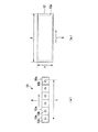
本実施形態に係る画像表示装置1は、図1に示すように、複数のレーザ光を射出するレーザ光源10と、レーザ光源10から射出されたレーザ光の照度分布を均一化するマイクロレンズアレイ11と、マイクロレンズアレイ11により均一化されたレーザ光が入射されるライトバルブ(光変調装置)12とを備えている。また、ライトバルブ12は、レーザ光源10から射出されたレーザ光を画像信号に応じて変調するものである。そして、ライトバルブ12により変調されたレーザ光は、投射レンズ(図示略)によりスクリーン(被投射面)15に投射される。
また、マイクロレンズアレイ11により均一化されたレーザ光はライトバルブ12の長手方向と短手方向とを有する光照明領域(画素領域)12a全面を照射するようになっている。
[First Embodiment]
A first embodiment of an image display device of the present invention will be described with reference to FIGS.
As shown in FIG. 1, the image display device 1 according to the present embodiment includes a
The laser light made uniform by the
レーザ光源10は、図2(a)に示すように、発光部10bを有する複数(本実施形態では6個)半導体レーザ素子(発光素子)10aが一方向に沿って個別に配列された半導体レーザアレイである。このような半導体レーザ素子10aの配列により、複数の半導体レーザ素子10aから射出されるレーザ光の発光部10bの両端間の距離はLとなっている。すなわち、本実施形態では、発光部10bが1列であるため、発光部10bの端部間の距離の長手方向が、半導体レーザ素子10aの配列方向Aとなっている。なお、半導体レーザ素子10aから射出されるレーザ光は可視光である。
また、マイクロレンズアレイ11は、半導体レーザ素子10aの配列方向Aと垂直な方向に2列設けられている。これにより、半導体レーザ素子10aから射出されたレーザ光は重畳されライトバルブ12を照明するようになっている。
As shown in FIG. 2A, the
The
また、ライトバルブ12は、図2(b)に示すように、光照明領域12aの水平方向の寸法が垂直方向の寸法に比べて長い長方形状となっている。すなわち、ライトバルブ12の横X対縦Yのアスペクト比は、例えば4対3や16対9である。また、図2(b)に示す矢印Bの方向がライトバルブ12の光照明領域12aの長手方向である。ここで、レーザ光源10は、図1に示すように、ライトバルブ12の光照明領域12aの長手方向Bがレーザ光源10の配列方向Aと一致するように配置されている。
As shown in FIG. 2B, the
本実施形態に係る画像表示装置1では、レーザ光源10の配列方向Aと、ライトバルブ12の光照明領域12aの長手方向Bとが一致するように、レーザ光源10が配置されているため、ライトバルブ12に入射するレーザ光源10から射出された複数のレーザ光の入射角度を小さくすることができる。
すなわち、例えば、図3(a)に示すように、レーザ光源10の配列方向Aをライトバルブ12の光照明領域12aの長手方向Bに対して垂直に配置した場合のライトバルブ12の入射端面12aに対するレーザ光の入射角度をθ2とする。この場合、レーザ光源10の短手方向A2とライトバルブ12の光照明領域12aの長手方向Bとが一致している。
一方、図3(b)に示すように、本実施形態のライトバルブ12の入射端面12aに対するレーザ光の入射角度をθ1とすると、マイクロレンズアレイ11によりレーザ光を大きく曲げる必要がないため、入射角θ2に比べθ1の方が小さくなる。特にライトバルブ12として、液晶ライトバルブを用いた場合、レーザ光源の配置を考慮しないと、ライトバルブ12に入射するレーザ光の入射角度が大きくなってしまい、コントラストが低下してしまう。しかしながら、本実施形態の画像表示装置1を用いることにより、画像のコントラストの向上が実現できる。
In the image display device 1 according to the present embodiment, since the
That is, for example, as shown in FIG. 3A, the incident end face 12 a of the
On the other hand, as shown in FIG. 3B, if the incident angle of the laser beam with respect to the
さらに、本発明の画像表示装置1は、ライトバルブ12に対する入射角度θ1を低く抑えることができるため、レーザ光の利用効率を向上させることが可能となる。したがって、投射レンズのFナンバーを小さくして明るい光学系を得る必要がないため、高価な投射レンズを用いなくても良い。すなわち、低コスト化を図りつつ、明るい画像をスクリーン15に投射することが可能となる。
つまり、本実施形態の画像表示装置1は、ライトバルブ12を効率良く均一に照明し、画像のコントラストを向上させることが可能である。
Furthermore, since the image display apparatus 1 of the present invention can keep the incident angle θ1 with respect to the
That is, the image display apparatus 1 of the present embodiment can efficiently and uniformly illuminate the
[第1実施形態の変形例]
図1に示す第1実施形態では、レーザ光源10から射出された複数のレーザ光を均一化する手段としてマイクロレンズアレイを用いたが、マイクロレンズアレイ11に代えてホログラム素子を用いても良い。本変形例に係る画像表示装置に用いられるホログラム素子としては、例えば、ホログラム原板に計算機で計算して人工的に作成した干渉縞が形成された計算機ホログラム(CGH:Computer Generated Hologram)を用いることがきできる。計算機ホログラムは、回折格子の分割領域の自由な設定が可能であり、収差の問題が生じないので好適である。このようなホログラム素子を用いた場合も第1実施形態と同様に、ホログラム素子から射出されたレーザ光はライトバルブの全面を照射するようになっている。
本変形例に係る画像表示装置では、ライトバルブを照明するレーザ光は平行性が良いため、スクリーンに鮮明で高コントラストな画像を表示することが可能となる。
[Modification of First Embodiment]
In the first embodiment shown in FIG. 1, a microlens array is used as means for uniformizing a plurality of laser beams emitted from the
In the image display device according to this modification, the laser light that illuminates the light valve has good parallelism, so that a clear and high-contrast image can be displayed on the screen.
[第2実施形態]
次に、本発明に係る第2実施形態について、図4を参照して説明する。なお、以下に説明する各実施形態において、上述した第1実施形態に係る画像表示装置1と構成を共通とする箇所には同一符号を付けて、説明を省略することにする。
第1実施形態では、マイクロレンズアレイ11から射出されたレーザ光によりライトバルブ12の光照明領域12aの全面を照射したが、本実施形態に係る画像表示装置30では、線状のレーザビームにより1次元ライトバルブ33を照射する。
[Second Embodiment]
Next, a second embodiment according to the present invention will be described with reference to FIG. In each embodiment described below, portions having the same configuration as those of the image display device 1 according to the first embodiment described above are denoted by the same reference numerals and description thereof is omitted.
In the first embodiment, the entire surface of the
画像表示装置30は、図4に示すように、複数のレーザ光を射出するレーザ光源31と、ホログラム素子(光学素子)32と、1次元ライトバルブ33と、スキャンミラー(走査手段)34とを備えている。
レーザ光源31は、複数の発光部31aが一方向に沿って並んで配列された半導体レーザバーである。このような発光部31aの配列により、発光部31bの端部間の距離の長手方向が、発光部31aの配列方向A1となっている。また、レーザ光源31は、第1実施形態と同様に、当該レーザ光源31の発光部31bの配列方向A1と1次元ライトバルブ33の光照明領域33bの長手方向B1とが合うように配置されている。
As shown in FIG. 4, the
The
ホログラム素子32は、レーザ光源31から射出されたレーザ光をレーザ光源31の発光部31aの長手方向A1に沿った線状のレーザ光Dに変換する光学素子である。また、このホログラム素子32は、第1実施形態の変形例で用いた計算機ホログラムである。
The
また、1次元ライトバルブ33は、透過型の液晶素子であり、光変調画素33aが1次元に配列された1次元光変調装置である。ここで、レーザ光Dの幅(発光部33aの配列方向A1と垂直な方向の寸法)は、ほぼ光変調画素33aの幅(1次元ライトバルブ33の長手方向B1と垂直な方向の寸法)と等しくなっている。
また、1次元ライトバルブ33とスクリーン15との間には、スキャンミラー(走査手段)34が設けられている。このスキャンミラー34は、1次元ライトバルブ33より変調されたレーザ光をスクリーン15に向かって走査するものである。つまり、1次元ライトバルブ33から射出されたレーザ光は、スキャンミラー34において反射されスクリーン15の矢印Hで示す水平方向に投射される。また、水平方向に投射されたレーザ光は、スキャンミラー34により、スクリーン15の矢印Vで示す垂直方向の走査を行うようになっている。
The one-
A scan mirror (scanning means) 34 is provided between the one-
本実施形態に係る画像表示装置30では、第1実施形態の画像表示装置1と同様の効果を得ることができる。さらに、本実施形態の画像表示装置30では、ホログラム素子32により、1次元ライトバルブ33に入射されるレーザ光は線状のレーザ光に変換されるため、1次元ライトバルブ33に入射するレーザ光の入射角をより小さくすることが可能となる。したがって、スクリーン15に投射される画像のコントラストをより向上させることが可能となる。
The
また、1次元ライトバルブ33が1次元の光変調装置であるため、レーザ光源10から射出されたレーザ光は1次元ライトバルブ33に均一に照明され易くなる。すなわち、均一なレーザ光が1次元ライトバルブ33から射出されるため、輝度ムラのない高コントラストな画像をスクリーン15に投射することが可能となる。
なお、本実施形態において、1次元光変調装置として透過型の液晶素子を用いたが、反射型の液晶素子、GLV等であっても良い。
Further, since the one-
In the present embodiment, a transmissive liquid crystal element is used as the one-dimensional light modulator, but a reflective liquid crystal element, GLV, or the like may be used.
[第3実施形態]
次に、本発明に係る第3実施形態について、図5及び図6を参照して説明する。
本実施形態に係る画像表示装置40では、線状のレーザビームにより2次元のライトバルブ45を照射する点において第2実施形態と異なる。
[Third Embodiment]
Next, a third embodiment according to the present invention will be described with reference to FIGS.
The
画像表示装置40は、図5に示すように、第1実施形態と同様の半導体レーザバーであるレーザ光源41と、ホログラム素子(光学素子)42と、シリンドリカルレンズ43と、スキャンミラー(走査手段)44と、2次元ライトバルブ(光変調装置)45とを備えている。
As shown in FIG. 5, the
ホログラム素子42は、レーザ光源10から射出されたレーザ光を線状のレーザ光Fに変換し、シリンドリカルレンズ43の入射端面43aに入射させる光学素子である。このホログラム素子42は、第1実施形態の変形例で用いた計算機ホログラムである。
シリンドリカルレンズ43は、入射されたレーザ光を平行光に変換させるものである。また、スキャンミラー44は、シリンドリカルレンズ43により平行化された線状のレーザ光を2次元ライトバルブ45に向かって走査するものである。
The
The cylindrical lens 43 converts incident laser light into parallel light. The
2次元ライトバルブ45は、図6に示すように、光変調画素45aが2次元に配列された2次元光変調装置である。また、2次元ライトバルブ45は、データの書き込みについては、3つのエリアごとに線順次でデータの書き換えが行われている。そして、各画素データがほぼ目標値となった場所、すなわち、図6に示す2次元ライトバルブ45のデータが確定したエリアGから順に線状のレーザ光Sが照射される。
ここで言う確定したエリアGとは、複数の光変調画素45aのうち、偏光板で検波した時の所定の透過率に到達したエリアを指している。すなわち、液晶ライトバルブの場合、各光変調画素45aは所定の透過率に到達するまでの時間が遅いので、レーザ光を照射しても所定の透過率に到達していないことがある。そこで、本実施形態のように、所定の透過率に到達したエリアにレーザ光を照射することによって、目標の光量を得ることができる。
As shown in FIG. 6, the two-
The defined area G mentioned here refers to an area that reaches a predetermined transmittance when detected by the polarizing plate among the plurality of
本実施形態に係る画像表示装置40では、第2実施形態の画像表示装置30と同様の効果を得ることができる。さらに、本実施形態の画像表示装置40では、均一なレーザ光が2次元ライトバルブ45に照射されるため、輝度ムラのない高コントラストな画像をスクリーン15に投射することが可能となる。また、本発明の画像表示装置40は、データが確定したエリアGに線状のレーザ光Sを照射することができるので、特に、光変調装置として液晶パネルを用いて動画を表示する際に、移動物体が尾を引くように表示される、いわゆる「尾引き」現象の発生を抑えることが可能となる。したがって、動画特性に優れた画像表示装置40を提供することが可能となる。
なお、シリンドリカルレンズ44を用いたが、これに限らず、入射されたレーザ光を平行光に変換させるレンズであれば良い。
The
Although the
[第4実施形態]
次に、本発明に係る第4実施形態について、図7及び図8を参照して説明する。
本実施形態に係る画像表示装置50では、レーザ光源51が第1レーザアレイ51A及び第2レーザアレイ51Bを備える点において第3実施形態と異なる。
[Fourth Embodiment]
Next, a fourth embodiment according to the present invention will be described with reference to FIGS.
The
レーザ光源51は、図7に示すように、一方向に沿って配列された複数の半導体レーザ素子51aを有する第1レーザアレイ51Aと、半導体レーザ素子51aの配列方向と同じ方向に沿って配列された複数の半導体レーザ素子51bを有する第2レーザアレイ51Bとを備えている。また、レーザ光源51は、半導体レーザ素子51aの配列方向と垂直な方向に、第1,第2レーザアレイ51A,51Bが2列並んで配列されている。
As shown in FIG. 7, the
第1レーザアレイ51Aから射出されたレーザ光は、マイクロレンズアレイ52aにより均一化されるとともに、線状のレーザ光に変換される。また、同様に、第2レーザアレイ51Bから射出されたレーザ光は、マイクロレンズアレイ52bにより均一化されるとともに、線状のレーザ光に変換される。
そして、半導体レーザ素子51aのレーザビームは第3実施形態と同様にスキャンミラー44により走査され、図8に示す2次元ライトバルブ45のデータが確定したエリアGから順に線状のレーザ光S1が照射される。また、同様に、半導体レーザ素子51bのレーザビームは第3実施形態と同様にスキャンミラー44により走査され、エリアGから順に線状のレーザ光S2が照射される。
The laser light emitted from the
Then, the laser beam of the
次に、第1レーザアレイ51A及び第2レーザアレイ51Bの駆動について説明する。
第1レーザアレイ51A及び第2レーザアレイ51Bは、独立に駆動させることが可能となっている。そして、各線状のレーザ光S1及びレーザ光S2は、2次元ライトバルブ45上を走査しているときのみに独立にそれぞれが点灯する。
具体的には、第2レーザアレイ51Bによるレーザ光S2が2次元ライトバルブ45に入射するときに、第2レーザアレイ51Bが点灯する。このとき、第1レーザアレイ51Aによるレーザ光S1は2次元ライトバルブ45上にないため、第1レーザアレイ51Aは消灯している。その後、レーザ光S1が2次元ライトバルブ45に入るとき、第1レーザアレイ51Aが点灯する。そして、レーザ光S1,レーザ光S2は、所定の間隔を保ちながら、2次元ライトバルブ45上を照明する。
Next, driving of the
The
Specifically, when the laser beam S2 from the
また、レーザ光S1,S2が2次元ライトバルブ45の下側に到達したときも同様に、第2レーザアレイ51Bによるレーザ光S2が2次元ライトバルブ45から出るときに、第2レーザアレイ51Bは消灯する。このとき、第1レーザアレイ51Aによるレーザ光S1は2次元ライトバルブ45上に残っているため点灯している。その後、第1レーザアレイ51Aによるレーザ光S1が2次元ライトバルブ45から出るときに、第1レーザアレイ51Aは消灯する。
Similarly, when the laser beams S1 and S2 reach the lower side of the two-
本実施形態に係る画像表示装置50では、第3実施形態の画像表示装置40と同様の効果を得ることができる。さらに、本実施形態の画像表示装置50では、レーザ光源51が2列の第1,第2レーザアレイ51A,51Bを備えているので、それぞれのレーザアレイ51A,51Bから射出される線状のレーザ光S1,S2により2次元ライトバルブ45を照明することになる。したがって、レーザ光S1,S2を2次元ライトバルブ45の水平方向に角度を付けて入射させる必要がないため、2次元ライトバルブ45に入射するレーザ光S1,S2の入射角度を小さくすることができる。
なお、本実施形態では、2列の発光部51a,51bを有するレーザ光源について説明したが、3列以上であっても良い。
The
In the present embodiment, a laser light source having two rows of light emitting
[第5実施形態]
次に、本発明に係る第5実施形態について、図9を参照して説明する。
本実施形態に係る画像表示装置60では、マイクロレンズアレイ52a,52bに代えてホログラム素子61を備える点において第4実施形態と異なる。
第4実施形態では、レーザアレイの列と同じ本数の線状のレーザ光に変換したが、第2実施形態のように1次元ライトバルブを用いた場合、1本の照明にする必要が生じる。また、非常に狭い各レーザの間隔での複数の照明でも良いが、この場合、レーザ光の間隔をレーザアレイの列間隔より狭くする必要が生じる。これらの場合、複数のレーザアレイから射出されたレーザ光はレーザアレイの列位置以外の場所を照明する必要がある。そこで、本実施形態では、第4実施形態の画像表示装置50のマイクロレンズアレイ52a,52bに代えて、ホログラム素子61を用いてレーザアレイの列位置以外の場所を照明する画像表示装置60について説明する。
[Fifth Embodiment]
Next, a fifth embodiment according to the present invention will be described with reference to FIG.
The
In the fourth embodiment, the laser beam is converted into the same number of linear laser beams as the laser array columns. However, when a one-dimensional light valve is used as in the second embodiment, it is necessary to use one illumination. In addition, a plurality of illuminations with very narrow intervals between the lasers may be used, but in this case, it is necessary to make the interval between the laser beams narrower than the column interval of the laser array. In these cases, it is necessary for the laser beams emitted from the plurality of laser arrays to illuminate places other than the column positions of the laser arrays. Therefore, in this embodiment, an
ホログラム素子61は、第1レーザアレイ51A及び第2レーザアレイ51Bのそれぞれから射出されたレーザ光を1ヶ所に集光させ、線状のレーザ光Jに変換する光学素子である。また、各レーザアレイ51A,51Bから射出されたレーザ光は、ホログラム素子61により、第1レーザアレイ51Aから射出されたレーザ光の0次光の光路01と第2レーザアレイ51Bから射出されたレーザ光の0次光の光路02との間に集光される。本実施形態は、2つのレーザ光を1つのレーザ光にすることにより、1次元ライトバルブを照明するのに好適である。
The hologram element 61 is an optical element that condenses the laser light emitted from each of the
本実施形態に係る画像表示装置60では、第4実施形態の画像表示装置50と同様の効果を得ることができる。さらに、本実施形態の画像表示装置60では、ホログラム素子61は、第1,第2レーザアレイ51A,51Bから射出されたそれぞれのレーザ光を当該レーザ光の0次光の光路01,02上以外に集光させる。これにより、画像の表示に影響を与える0次光がライトバルブに照明されることがないため、より鮮明な画像をスクリーンに投射することが可能となる。
特に、レーザ光源51から射出されたレーザ光を0次光の光路01と0次光の光路02との間に集光させることで、第1レーザアレイ51A及び第2レーザアレイ51Bから射出された両方とものライトバルブに入射するレーザ光の入射角を抑えることが可能となる。
The
In particular, the laser light emitted from the
[第6実施形態]
次に、本発明に係る第6実施形態について、図10を参照して説明する。
本実施形態に係る画像表示装置70では、光変調装置が液晶ライトバルブ(液晶素子)71であり、マイクロレンズアレイ11と液晶ライトバルブ71との間に1/2波長板(位相差板)72を備える点において第1実施形態と異なる。
つまり、液晶ライトバルブを照明する場合、半導体レーザ素子のアレイ方向とライトバルブとの長辺方向を一致させ、レーザ光の偏光方向とライトバルブの入射光の偏光方向も一致させる必要がある。
そこで、本実施形態は、半導体レーザ素子のアレイ方向とレーザ光源から射出されるレーザ光の偏光方向とが決まっている場合、半導体レーザ素子のアレイ方向とライトバルブの長辺方向との一致を優先させ、1/2波長板72によりレーザ光の偏光面をライトバルブの入射側の偏光方向に一致させる構成である。
[Sixth Embodiment]
Next, a sixth embodiment according to the present invention will be described with reference to FIG.
In the
That is, when illuminating the liquid crystal light valve, the array direction of the semiconductor laser elements and the long side direction of the light valve must be matched, and the polarization direction of the laser light and the polarization direction of the incident light of the light valve must also be matched.
Therefore, in this embodiment, when the array direction of the semiconductor laser element and the polarization direction of the laser light emitted from the laser light source are determined, priority is given to matching the array direction of the semiconductor laser element and the long side direction of the light valve. The polarization plane of the laser light is made to coincide with the polarization direction on the incident side of the light valve by the half-
具体的には、レーザ光源10は、矢印で示すように、S偏光のレーザ光を射出するものである。
液晶ライトバルブ71の入射端面71a側には入射側偏光板73が設けられ、射出端面71bには射出側偏光板74が設けられている。この入射側偏光板73は、P偏光のレーザ光を入射させ、射出側偏光板74は、S偏光のレーザ光を射出させるものである。
このとき、レーザ光源10から射出されたP偏光のレーザ光は、1/2波長板72によりS偏光のレーザ光に変換される。そして、入射側偏光板73を介して液晶ライトバルブ71に入射する。
Specifically, the
An incident-side
At this time, the P-polarized laser light emitted from the
本実施形態に係る画像表示装置70では、第1実施形態の画像表示装置1と同様の効果を得ることができる。さらに、本実施形態の画像表示装置70では、本実施形態のようにレーザ光源10から射出されたレーザ光の偏光方向と液晶ライトバルブ71の入射側の偏光方向とが一致していない場合に有効である。すなわち、1/2波長板72により、レーザ光源10から射出されたレーザ光の偏光面が回転されるため、レーザ光を液晶ライトバルブ71の入射側の偏光方向に一致させることができる。したがって、光の利用効率を向上させることができるため、より明るい画像を得ることが可能となる。
なお、本実施形態において、位相差板として1/2波長板72を用いたが、レーザ光源10から射出されるレーザ光の偏光方向と、入射側偏光板の偏光方向とに応じて適宜変更が可能である。
また、半導体レーザ素子の実装で偏光方向を合わせられる場合は、実装の際に偏光方向を合わせることが好ましい。
The
In the present embodiment, the half-
When the polarization direction can be adjusted by mounting the semiconductor laser element, it is preferable to adjust the polarization direction at the time of mounting.
なお、本発明の技術範囲は上記実施形態に限定されるものではなく、本発明の趣旨を逸脱しない範囲において種々の変更を加えることが可能である。
例えば、上記各実施形態におけるレーザ光源としては、発光部を有する素子が個別に設けられたレーザアレイ、あるいは、レーザバーにより構成された光源を用いたが、いずれの光源を用いても良い。また、レーザ光源として、図11に示すように、複数の発光部を有する面発光レーザアレイ81を用いても良い。この場合、2列側の両端の発光部間の距離L1と4列側の両端の発光部間の距離L2とでは、距離L2の方が長いのでこの4列側の配列方向を長手方向とする。
すなわち、本発明で言う光源装置の長手方向とは、発光部の数や、レーザ光源の外形の長さに関係するものではなく、発光部の端部間の距離の長い方を長手方向としている。
さらに、レーザ光源は、複数の発光部から射出されたレーザ光を光ファイバに入射させた後一つにまとめたものであっても良い。
また、これらのレーザ光源にはヒートシンクが設けられ、発光部が発光する際に生じる熱を放熱する構成にしても良い。
The technical scope of the present invention is not limited to the above embodiment, and various modifications can be made without departing from the spirit of the present invention.
For example, as the laser light source in each of the above-described embodiments, a laser array in which elements having light emitting units are individually provided or a light source constituted by a laser bar is used, but any light source may be used. As a laser light source, as shown in FIG. 11, a surface emitting
That is, the longitudinal direction of the light source device referred to in the present invention is not related to the number of light emitting portions or the length of the outer shape of the laser light source, but the longer direction between the end portions of the light emitting portions is the longitudinal direction. .
Furthermore, the laser light source may be one in which laser light emitted from a plurality of light emitting units is made incident after being incident on the optical fiber.
Further, these laser light sources may be provided with a heat sink to dissipate heat generated when the light emitting unit emits light.
また、発光部から射出されるレーザ光は可視光であったが、図12に示すように、赤外光を射出する発光部を有するレーザ光源85であっても良い。この場合、レーザ光源45の後段に、波長変換素子86を配置することにより、発光部から射出されたレーザ光は所定の波長に変換される。さらには、より波長変換効率を上げるために、波長変換素子86の後段に外部共振器を設けた構成であっても良い。
Further, the laser light emitted from the light emitting unit is visible light, but as shown in FIG. 12, a
1,30,40,50,60…画像表示装置、10…レーザ光源、10a…半導体レーザ素子(素子)、12…ライトバルブ(光変調装置)、12a,33a…光照明領域、32,42,61…ホログラム素子(光学素子)、33…1次元ライトバルブ(光変調装置)、34,44…スキャンミラー(走査手段)、45…2次元ライトバルブ(光変調装置)、71…液晶ライトバルブ(液晶素子)
DESCRIPTION OF
Claims (3)
該レーザ光源から射出されたレーザ光を画像信号に応じて変調し、複数の光変調画素が1次元に配列された1次元光変調装置であって、液晶素子からなる光変調装置と、
前記レーザ光源から射出され前記光変調装置に照射されるレーザ光を線状のレーザ光に変換するホログラム素子からなる光学素子と、
前記1次元光変調装置と前記被投射面との間に配置され、前記1次元光変調装置から射出された線状のレーザ光を前記被投射面に向かって走査する走査手段と、を備え、
前記レーザ光源の発光部列を構成する発光部の端部間の距離の長手方向と前記光変調装置の光照明領域の長手方向とが一致しており、
前記光学素子が、前記レーザ光源から射出されたレーザ光を前記発光部列の列数未満の本数の線状のレーザ光に変換するとともに各列の前記発光部から射出されたレーザ光の0次光の光路上以外に集光させることを特徴とする画像表示装置。 A laser light source having a plurality of light emitting part rows including a plurality of light emitting parts arranged in one direction;
A one-dimensional light modulation device in which a laser beam emitted from the laser light source is modulated in accordance with an image signal and a plurality of light modulation pixels are arranged one-dimensionally, and a light modulation device including a liquid crystal element;
An optical element composed of a hologram element that converts laser light emitted from the laser light source and applied to the light modulation device into linear laser light ;
A scanning unit disposed between the one-dimensional light modulator and the projection surface, and scanning linear laser light emitted from the one-dimensional light modulator toward the projection surface ;
The longitudinal direction of the distance between the end portions of the light emitting units constituting the light emitting unit row of the laser light source matches the longitudinal direction of the light illumination region of the light modulation device,
The optical element converts laser light emitted from the laser light source into linear laser light having a number less than the number of rows of the light emitting unit rows and zeroth order of the laser light emitted from the light emitting units of each row. An image display apparatus that collects light other than on an optical path of light.
前記ホログラム素子が、前記第1の発光部列および前記第2の発光部列のそれぞれから射出されたレーザ光を、前記第1の発光部列から射出されたレーザ光の0次光の光路と前記第2の発光部列から射出されたレーザ光の0次光の光路との間に集光させることを特徴とする請求項1に記載の画像表示装置。 The laser light source has a first light emitting part row and a second light emitting part row,
The hologram element emits laser light emitted from each of the first light emitting part row and the second light emitting part row to an optical path of zero-order light of the laser light emitted from the first light emitting part row. 2. The image display device according to claim 1, wherein the light is condensed between an optical path of zero-order light of the laser light emitted from the second light emitting unit row.
Priority Applications (5)
| Application Number | Priority Date | Filing Date | Title |
|---|---|---|---|
| JP2006239437A JP4483840B2 (en) | 2006-09-04 | 2006-09-04 | Image display device |
| US11/892,794 US8192029B2 (en) | 2006-09-04 | 2007-08-27 | Image display device |
| TW096131763A TW200825615A (en) | 2006-09-04 | 2007-08-28 | Image display device |
| KR1020070087569A KR20080022046A (en) | 2006-09-04 | 2007-08-30 | Image display |
| CN2007101478896A CN101140413B (en) | 2006-09-04 | 2007-08-31 | image display device |
Applications Claiming Priority (1)
| Application Number | Priority Date | Filing Date | Title |
|---|---|---|---|
| JP2006239437A JP4483840B2 (en) | 2006-09-04 | 2006-09-04 | Image display device |
Publications (2)
| Publication Number | Publication Date |
|---|---|
| JP2008064794A JP2008064794A (en) | 2008-03-21 |
| JP4483840B2 true JP4483840B2 (en) | 2010-06-16 |
Family
ID=39150998
Family Applications (1)
| Application Number | Title | Priority Date | Filing Date |
|---|---|---|---|
| JP2006239437A Expired - Fee Related JP4483840B2 (en) | 2006-09-04 | 2006-09-04 | Image display device |
Country Status (5)
| Country | Link |
|---|---|
| US (1) | US8192029B2 (en) |
| JP (1) | JP4483840B2 (en) |
| KR (1) | KR20080022046A (en) |
| CN (1) | CN101140413B (en) |
| TW (1) | TW200825615A (en) |
Cited By (1)
| Publication number | Priority date | Publication date | Assignee | Title |
|---|---|---|---|---|
| US11204587B2 (en) | 2018-11-08 | 2021-12-21 | Samsung Electronics Co., Ltd. | Holographic display apparatus |
Families Citing this family (10)
| Publication number | Priority date | Publication date | Assignee | Title |
|---|---|---|---|---|
| JP6432637B2 (en) * | 2011-04-15 | 2018-12-05 | 大日本印刷株式会社 | Illumination device, projection device, and projection-type image display device |
| JP6160144B2 (en) * | 2013-03-15 | 2017-07-12 | セイコーエプソン株式会社 | Lighting device and projector |
| DE102014216390A1 (en) * | 2014-08-19 | 2016-02-25 | Siemens Aktiengesellschaft | projector |
| US10036803B2 (en) * | 2014-10-20 | 2018-07-31 | Quanergy Systems, Inc. | Three-dimensional lidar sensor based on two-dimensional scanning of one-dimensional optical emitter and method of using same |
| CN109038209B (en) * | 2018-08-29 | 2020-04-14 | Oppo(重庆)智能科技有限公司 | Wafer level packaging method, laser module, camera assembly and electronic device |
| CN110928123A (en) * | 2018-09-19 | 2020-03-27 | 青岛海信激光显示股份有限公司 | Laser array, laser light source and laser projection equipment |
| WO2020057124A1 (en) | 2018-09-19 | 2020-03-26 | 青岛海信激光显示股份有限公司 | Laser array, laser light source and laser projection device |
| DE102019106674A1 (en) * | 2019-03-15 | 2020-09-17 | OSRAM Opto Semiconductors Gesellschaft mit beschränkter Haftung | Device and method for projecting a plurality of focal points onto a surface |
| TWI723660B (en) * | 2019-09-09 | 2021-04-01 | 英錡科技股份有限公司 | Laser projection system, wearable image projection device and method for improving laser projection image |
| CN111490458A (en) * | 2020-06-01 | 2020-08-04 | 浙江水晶光电科技股份有限公司 | Laser Display, Preset Range of Divergence Angle and Determination Method of Fiber Length |
Family Cites Families (24)
| Publication number | Priority date | Publication date | Assignee | Title |
|---|---|---|---|---|
| JPH0425290A (en) | 1990-05-21 | 1992-01-29 | Victor Co Of Japan Ltd | Display device |
| DE69123288T2 (en) * | 1990-05-21 | 1997-04-24 | Victor Company Of Japan | Display device |
| JP2627032B2 (en) | 1991-06-19 | 1997-07-02 | ソニー・テクトロニクス株式会社 | Liquid crystal cell type video projector |
| JPH10319873A (en) | 1997-05-15 | 1998-12-04 | Mitsubishi Electric Corp | Light source unit and display device, display and illumination device using it |
| JP4374624B2 (en) * | 1997-09-22 | 2009-12-02 | ソニー株式会社 | Video display device |
| JPH11174320A (en) | 1997-12-17 | 1999-07-02 | Fuji Xerox Co Ltd | Optical projection system and image forming device |
| JP3347072B2 (en) | 1998-09-16 | 2002-11-20 | 株式会社東芝 | Polycrystalline growth method |
| JP4080608B2 (en) | 1998-09-25 | 2008-04-23 | 浜松ホトニクス株式会社 | Semiconductor laser light source device |
| JP4182374B2 (en) | 1998-10-29 | 2008-11-19 | ソニー株式会社 | Projection display |
| US6511186B1 (en) * | 1999-07-09 | 2003-01-28 | Sarnoff Corporation | Focus and aim device and method for image projection |
| JP2001021719A (en) | 1999-07-12 | 2001-01-26 | Seiko Epson Corp | Polarization separation element, polarization conversion element, and projection display device |
| JP2002072360A (en) | 2000-08-29 | 2002-03-12 | Sony Corp | Picture display device |
| JP4646278B2 (en) | 2000-10-26 | 2011-03-09 | 株式会社リコー | Illumination optical system and projection device |
| JP3952867B2 (en) | 2001-12-07 | 2007-08-01 | 株式会社ジェイテクト | Laser concentrator |
| JP2003222727A (en) | 2002-01-31 | 2003-08-08 | Hitachi Chem Co Ltd | Optical control diffusion element by holography |
| US7088353B2 (en) * | 2002-07-10 | 2006-08-08 | Fuji Photo Film Co., Ltd. | Display device |
| KR100828531B1 (en) * | 2002-07-26 | 2008-05-13 | 삼성전자주식회사 | Liquid crystal display |
| US7006543B2 (en) * | 2002-08-30 | 2006-02-28 | Primarion, Inc. | System and circuit for a multi-channel optoelectronic device driver |
| JP3458856B2 (en) | 2002-10-07 | 2003-10-20 | 富士ゼロックス株式会社 | Image recording device |
| JP2004146456A (en) | 2002-10-22 | 2004-05-20 | Hamamatsu Photonics Kk | Semiconductor laser device |
| US6947459B2 (en) * | 2002-11-25 | 2005-09-20 | Eastman Kodak Company | Organic vertical cavity laser and imaging system |
| JP2004264776A (en) | 2003-03-04 | 2004-09-24 | Seiko Epson Corp | Projector and optical device |
| CN1624570A (en) * | 2003-12-03 | 2005-06-08 | 精工爱普生株式会社 | Projector |
| US7910499B2 (en) | 2004-11-12 | 2011-03-22 | Applied Materials, Inc. | Autofocus for high power laser diode based annealing system |
-
2006
- 2006-09-04 JP JP2006239437A patent/JP4483840B2/en not_active Expired - Fee Related
-
2007
- 2007-08-27 US US11/892,794 patent/US8192029B2/en not_active Expired - Fee Related
- 2007-08-28 TW TW096131763A patent/TW200825615A/en unknown
- 2007-08-30 KR KR1020070087569A patent/KR20080022046A/en not_active Application Discontinuation
- 2007-08-31 CN CN2007101478896A patent/CN101140413B/en not_active Expired - Fee Related
Cited By (1)
| Publication number | Priority date | Publication date | Assignee | Title |
|---|---|---|---|---|
| US11204587B2 (en) | 2018-11-08 | 2021-12-21 | Samsung Electronics Co., Ltd. | Holographic display apparatus |
Also Published As
| Publication number | Publication date |
|---|---|
| TW200825615A (en) | 2008-06-16 |
| US20080055556A1 (en) | 2008-03-06 |
| KR20080022046A (en) | 2008-03-10 |
| CN101140413A (en) | 2008-03-12 |
| JP2008064794A (en) | 2008-03-21 |
| US8192029B2 (en) | 2012-06-05 |
| CN101140413B (en) | 2011-08-03 |
Similar Documents
| Publication | Publication Date | Title |
|---|---|---|
| JP4483840B2 (en) | Image display device | |
| US7748853B2 (en) | Lighting device and projector | |
| US8469525B2 (en) | Projection-type display apparatus | |
| JP4552956B2 (en) | Lighting device and projector | |
| US8334937B2 (en) | Liquid crystal projector and image reproducing device | |
| CN107577112B (en) | Illumination device, projection type image display device, and optical device | |
| JP7135909B2 (en) | projector | |
| JP2004529375A5 (en) | ||
| US20100074284A1 (en) | Light source unit and image displaying apparatus using the same | |
| US20100177253A1 (en) | Coherent imaging method of laser projection and apparatus thereof | |
| US20090219491A1 (en) | Method of combining multiple Gaussian beams for efficient uniform illumination of one-dimensional light modulators | |
| US20120236212A1 (en) | Optical multiplexing apparatus and projector | |
| US20090141251A1 (en) | Illumination system to eliminate laser speckle and projection system employing the same | |
| JP2003218017A (en) | Laser lighting optical system, aligner using the same, laser processing device, and projection device | |
| JP3473075B2 (en) | Lighting device and projection display device | |
| JP2010276757A (en) | Projector and electro-optical device | |
| JP2008256823A (en) | Light source device and projector | |
| JP2016035509A (en) | Light source device and exposure apparatus | |
| US8136951B2 (en) | Projection type display apparatus and optical unit with optical coupling lens | |
| US20130250269A1 (en) | Exposure apparatus | |
| JP2009063892A (en) | Projector, optical element, and light modulation device | |
| JP2021089303A (en) | Light source device and image projection device | |
| JP3975948B2 (en) | Illumination device and projection device | |
| WO2015001736A1 (en) | Exposure device and lighting unit | |
| JP2009063893A (en) | Projector, optical element, and light modulation device |
Legal Events
| Date | Code | Title | Description |
|---|---|---|---|
| A977 | Report on retrieval |
Free format text: JAPANESE INTERMEDIATE CODE: A971007 Effective date: 20081017 |
|
| A131 | Notification of reasons for refusal |
Free format text: JAPANESE INTERMEDIATE CODE: A131 Effective date: 20081021 |
|
| A521 | Request for written amendment filed |
Free format text: JAPANESE INTERMEDIATE CODE: A523 Effective date: 20081218 |
|
| A131 | Notification of reasons for refusal |
Free format text: JAPANESE INTERMEDIATE CODE: A131 Effective date: 20090203 |
|
| A521 | Request for written amendment filed |
Free format text: JAPANESE INTERMEDIATE CODE: A523 Effective date: 20090406 |
|
| A131 | Notification of reasons for refusal |
Free format text: JAPANESE INTERMEDIATE CODE: A131 Effective date: 20091020 |
|
| A521 | Request for written amendment filed |
Free format text: JAPANESE INTERMEDIATE CODE: A523 Effective date: 20091130 |
|
| A521 | Request for written amendment filed |
Free format text: JAPANESE INTERMEDIATE CODE: A821 Effective date: 20091201 |
|
| TRDD | Decision of grant or rejection written | ||
| A01 | Written decision to grant a patent or to grant a registration (utility model) |
Free format text: JAPANESE INTERMEDIATE CODE: A01 Effective date: 20100302 |
|
| A01 | Written decision to grant a patent or to grant a registration (utility model) |
Free format text: JAPANESE INTERMEDIATE CODE: A01 |
|
| A61 | First payment of annual fees (during grant procedure) |
Free format text: JAPANESE INTERMEDIATE CODE: A61 Effective date: 20100315 |
|
| R150 | Certificate of patent or registration of utility model |
Ref document number: 4483840 Country of ref document: JP Free format text: JAPANESE INTERMEDIATE CODE: R150 Free format text: JAPANESE INTERMEDIATE CODE: R150 |
|
| FPAY | Renewal fee payment (event date is renewal date of database) |
Free format text: PAYMENT UNTIL: 20130402 Year of fee payment: 3 |
|
| FPAY | Renewal fee payment (event date is renewal date of database) |
Free format text: PAYMENT UNTIL: 20130402 Year of fee payment: 3 |
|
| FPAY | Renewal fee payment (event date is renewal date of database) |
Free format text: PAYMENT UNTIL: 20140402 Year of fee payment: 4 |
|
| S531 | Written request for registration of change of domicile |
Free format text: JAPANESE INTERMEDIATE CODE: R313531 |
|
| R350 | Written notification of registration of transfer |
Free format text: JAPANESE INTERMEDIATE CODE: R350 |
|
| LAPS | Cancellation because of no payment of annual fees |